DS92LV040A 4 Channel Bus LVDS Transceiver … 4 Channel Bus LVDS Transceiver 1 1 Features 1• Bus...
25
Copyright © 2018, Texas Instruments Incorporated DIN1 DE1 RO1 DIN2 RO2 DIN3 DE2 RO3 DIN4 RO4 RE1 RE2 DO1+/RI1+ DO1-/RI1- DO2+/RI2+ DO2-/RI2- DO3+/RI3+ DO3-/RI3- DO4+/RI4+ DO4-/RI4- Product Folder Order Now Technical Documents Tools & Software Support & Community An IMPORTANT NOTICE at the end of this data sheet addresses availability, warranty, changes, use in safety-critical applications, intellectual property matters and other important disclaimers. PRODUCTION DATA. DS92LV040A SNOS521E – JANUARY 2001 – REVISED JANUARY 2018 DS92LV040A 4 Channel Bus LVDS Transceiver 1 1 Features 1• Bus LVDS Signaling • Propagation Delay: Driver 2.3 ns Max, Receiver 3.2 ns Max • Low power CMOS Design • 100% Transition Time 1 ns Driver Typical, 1.3 ns Receiver Typical • High Signaling Rate Capability (above 155 Mbps) • 0.1 V to 2.3 V Common Mode Range for V ID = 200 mV • 70 mV Receiver Sensitivity • Supports Open and Terminated Failsafe on Port Pins • 3.3-V Operation • Glitch Free Power up/down (Driver & Receiver Disabled) • Light Bus Loading (5 pF Typical) per Bus LVDS Load • Balanced Output Impedance • Product Offered in 44 Pin WQFN Package • High Impedance Bus Pins on Power Off (V CC = 0 V) 2 Applications Designed for Double Termination Applications 3 Description The DS92LV040A is one in a series of Bus LVDS transceivers designed specifically for high speed, low power backplane or cable interfaces. The device operates from a single 3.3-V power supply and includes four differential line drivers and four receivers. To minimize bus loading, the driver outputs and receiver inputs are internally connected. The device also features a flow through pin out which allows easy PCB routing for short stubs between its pins and the connector. The driver translates 3-V LVTTL levels (single-ended) to differential Bus LVDS (BLVDS) output levels. This allows for high speed operation while consuming minimal power and reducing EMI. In addition, the differential signaling provides common mode noise rejection greater than ±1 V. The receiver threshold is less than +0/−70 mV. The receiver translates the differential Bus LVDS to standard (LVTTL/LVCMOS) levels. (See the Application Information Section for more details.) Device Information (1) PART NUMBER PACKAGE BODY SIZE (NOM) DS92LV040A WQFN (44) 7.00 mm x 7.00 mm (1) For all available packages, see the orderable addendum at the end of the data sheet. Simplified Functional Diagram
-
Upload
truongkhanh -
Category
Documents
-
view
245 -
download
0
Transcript of DS92LV040A 4 Channel Bus LVDS Transceiver … 4 Channel Bus LVDS Transceiver 1 1 Features 1• Bus...
Copyright © 2018, Texas Instruments Incorporated
DIN1
DE1
RO1
DIN2
RO2
DIN3
DE2
RO3
DIN4
RO4
RE1
RE2
DO1+/RI1+
DO1-/RI1-
DO2+/RI2+
DO2-/RI2-
DO3+/RI3+
DO3-/RI3-
DO4+/RI4+
DO4-/RI4-
Product
Folder
Order
Now
Technical
Documents
Tools &
Software
Support &Community
An IMPORTANT NOTICE at the end of this data sheet addresses availability, warranty, changes, use in safety-critical applications,intellectual property matters and other important disclaimers. PRODUCTION DATA.
DS92LV040ASNOS521E –JANUARY 2001–REVISED JANUARY 2018
DS92LV040A 4 Channel Bus LVDS Transceiver
1
1 Features1• Bus LVDS Signaling• Propagation Delay: Driver 2.3 ns Max, Receiver
3.2 ns Max• Low power CMOS Design• 100% Transition Time 1 ns Driver Typical, 1.3 ns
Receiver Typical• High Signaling Rate Capability (above 155 Mbps)• 0.1 V to 2.3 V Common Mode Range for
VID = 200 mV• 70 mV Receiver Sensitivity• Supports Open and Terminated Failsafe on Port
Pins• 3.3-V Operation• Glitch Free Power up/down (Driver & Receiver
Disabled)• Light Bus Loading (5 pF Typical) per Bus LVDS
Load• Balanced Output Impedance• Product Offered in 44 Pin WQFN Package• High Impedance Bus Pins on Power Off
(VCC = 0 V)
2 ApplicationsDesigned for Double Termination Applications
3 DescriptionThe DS92LV040A is one in a series of Bus LVDStransceivers designed specifically for high speed, lowpower backplane or cable interfaces. The deviceoperates from a single 3.3-V power supply andincludes four differential line drivers and fourreceivers. To minimize bus loading, the driver outputsand receiver inputs are internally connected. Thedevice also features a flow through pin out whichallows easy PCB routing for short stubs between itspins and the connector.
The driver translates 3-V LVTTL levels (single-ended)to differential Bus LVDS (BLVDS) output levels. Thisallows for high speed operation while consumingminimal power and reducing EMI. In addition, thedifferential signaling provides common mode noiserejection greater than ±1 V.
The receiver threshold is less than +0/−70 mV. Thereceiver translates the differential Bus LVDS tostandard (LVTTL/LVCMOS) levels. (See theApplication Information Section for more details.)
Device Information(1)
PART NUMBER PACKAGE BODY SIZE (NOM)DS92LV040A WQFN (44) 7.00 mm x 7.00 mm
(1) For all available packages, see the orderable addendum atthe end of the data sheet.
Simplified Functional Diagram

2
DS92LV040ASNOS521E –JANUARY 2001–REVISED JANUARY 2018 www.ti.com
Product Folder Links: DS92LV040A
Submit Documentation Feedback Copyright © 2001–2018, Texas Instruments Incorporated
Table of Contents1 Features .................................................................. 12 Applications ........................................................... 13 Description ............................................................. 14 Revision History..................................................... 25 Pin Configuration and Functions ......................... 36 Specifications......................................................... 4
6.1 Absolute Maximum Ratings ...................................... 46.2 ESD Ratings.............................................................. 46.3 Recommended Operating Conditions....................... 46.4 Thermal Information .................................................. 46.5 DC Electrical Characteristics .................................... 56.6 AC Electrical Characteristics..................................... 6
7 Parameter Measurement Information .................. 67.1 Test Circuits and Timing Waveforms........................ 6
8 Detailed Description .............................................. 98.1 Overview ................................................................... 98.2 Functional Block Diagram ......................................... 9
8.3 Feature Description................................................... 98.4 Device Functional Modes........................................ 10
9 Application and Implementation ........................ 119.1 Application Information............................................ 119.2 Typical Application ................................................. 11
10 Power Supply Recommendations ..................... 1311 Layout................................................................... 14
11.1 Layout Guidelines ................................................. 1411.2 Layout Example .................................................... 17
12 Device and Documentation Support ................. 1912.1 Documentation Support ........................................ 1912.2 Receiving Notification of Documentation Updates 1912.3 Community Resources.......................................... 1912.4 Trademarks ........................................................... 1912.5 Electrostatic Discharge Caution............................ 1912.6 Glossary ................................................................ 19
13 Mechanical, Packaging, and OrderableInformation ........................................................... 19
4 Revision HistoryNOTE: Page numbers for previous revisions may differ from page numbers in the current version.
Changes from Revision D (April 2013) to Revision E Page
• Added Device Information table, ESD Ratings table, Feature Description section, Device Functional Modes,Application and Implementation section, Power Supply Recommendations section, Layout section, Device andDocumentation Support section, and Mechanical, Packaging, and Orderable Information section ..................................... 1
• Added "Driver Short Circuit Current Duration" to the Absolute Maximum Ratings ................................................................ 4• Deleted Note 4: "Only one output at a time should be shorted..." from the DC Electrical Characteristics table.................... 5
Changes from Revision C (April 2013) to Revision D Page
• Changed layout of National Data Sheet to TI format ............................................................................................................. 3
44N
C
1NC
43R
O4
13D
O4íR
I4í
2NC
32 NC
42D
IN4
14D
O4+
/RI4
+
3VCC
31 GND
41R
O3
15D
O3íR
I3í
4GND
30 VCC
40D
IN3
16D
O3+
/RI3
+
5RE34
29 RE12
39G
ND
17A
GN
D
6VCC
28 GND
38R
O2
18D
O2íR
I2í
7AVCC
27 AVCC
37D
IN2
19D
O2+
/RI2
+
8DE34
26 DE12
36R
O1
20D
O1íR
I1í
9AGND
25 AGND
35D
IN1
21D
O1+
/RI1
+
10AVCC
24 NC
22A
VC
C
23 NC
Not to scale
11NC
12NC
33 NC
34 NC
3
DS92LV040Awww.ti.com SNOS521E –JANUARY 2001–REVISED JANUARY 2018
Product Folder Links: DS92LV040A
Submit Documentation FeedbackCopyright © 2001–2018, Texas Instruments Incorporated
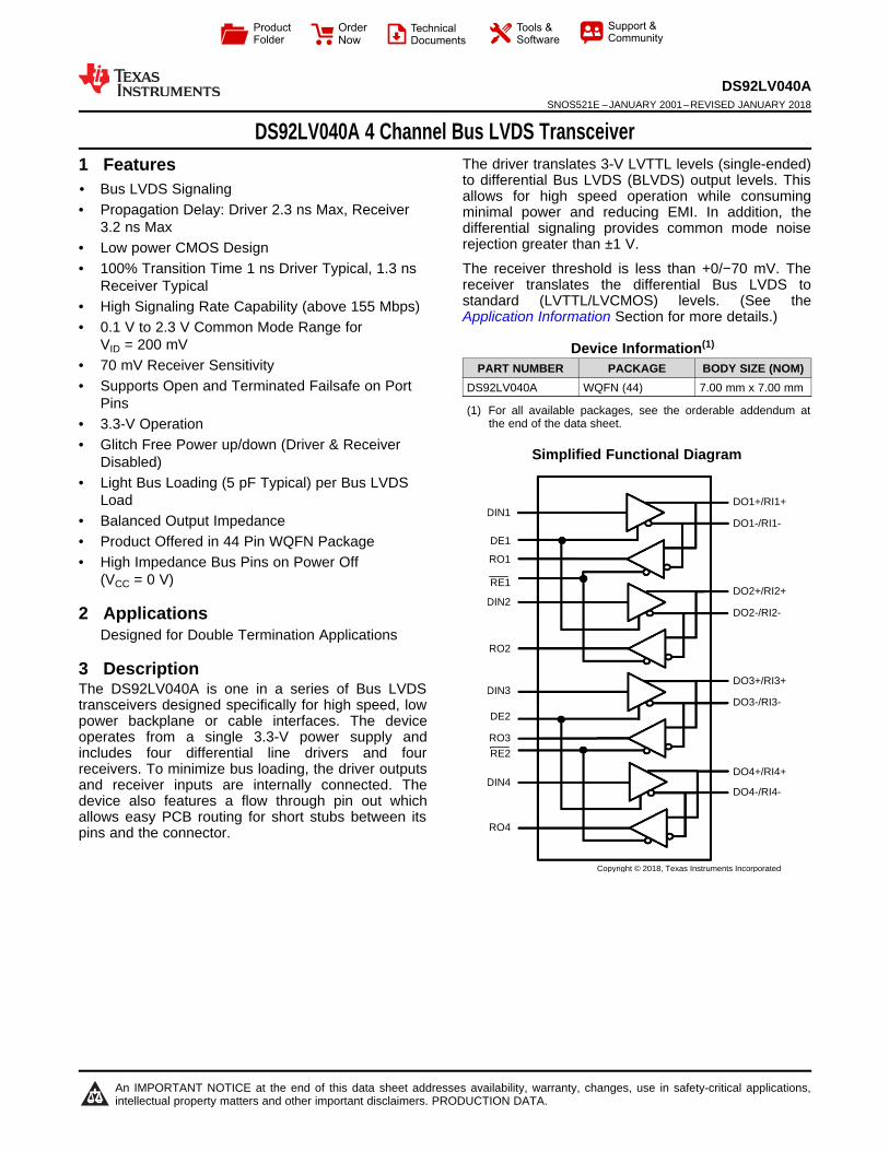
5 Pin Configuration and Functions
NJN PackageWQFN (44 Pin)
Top View
Pin FunctionsPIN NAME PIN # INPUT/
OUTPUTDESCRIPTIONS
DO+/RI+ 14, 16, 19, 21 I/O True Bus LVDS Driver Outputs and Receiver Inputs.
DO−/RI− 13, 15, 18, 20 I/O Complimentary Bus LVDS Driver Outputs and Receiver Inputs.
DIN 35, 37, 40, 42 I LVTTL Driver Input. No pull up or pull down is attached to this pin
RO 36, 38, 41, 43 O LVTTL Receiver Output.
RE12 29 IReceiver Enable LVTTL Input (Active Low). This pin, when low, configures receiver outputs, RO1 andRO2 active. When this pin is high, RO1 and RO2 are TRI-STATE. If this pin is floating, a weak currentsource to VCC causes RO1 and RO2 to be TRI-STATE
RE34 5 IReceiver Enable LVTTL Input (Active Low). This pin, when low, configures receiver outputs, RO3 andRO4 active. When this pin is high, RO3 and RO4 are TRI-STATE. If this pin is floating, a weak currentsource to VCC causes RO3 and RO4 to be TRI-STATE
DE12 26 I
Driver Enable LVTTL Input (Active High). This pin, when high, configures driver outputs, DO1+/RIN1+,DO1−/RIN1− and DO2+/RIN2+, DO2−/RIN2− active. When this pin is low, driver outputs 1 and 2 areTRI-STATE. If this pin is floating, a weak current source to VCC causes driver outputs 1 and 2 to beactive
DE34 8 I
Driver Enable LVTTL Input (Active High). This pin, when high, configures driver outputs, DO3+/RIN3+,DO3−/RIN3− and DO4+/RIN4+, DO4−/RIN4− active. When this pin is low, driver outputs 3 and 4 areTRI-STATE. If this pin is floating, a weak current source to VCC causes driver outputs 3 and 4 to beactive
GND 4, 28, 31, 39 Ground Ground for digital circuitry (must connect to GND on PC board). These pins connected internally.
VCC 3, 6, 30 Power VCC for digital circuitry (must connect to VCC on PC board). These pins connected internally.
AGND 9, 17, 25 Ground Ground for analog circuitry (must connect to GND on PC board). These pins connected internally.
AVCC 7, 10, 22, 27 Power Analog VCC (must connect to VCC on PC board). These pins connected internally.
NC 1, 2, 11, 12, 23, 24,32, 33, 34, 44 N/A Reserved for future use, leave open circuit.
DAP GNDMust connect to GND plane through vias to achieve the theta ja specified under Absolute MaximumRatings. The DAP (die attach pad) is the heat transfer material that is centered on the bottom of theWQFN package. Refer to application note AN-1187 () for attachment details.

4
DS92LV040ASNOS521E –JANUARY 2001–REVISED JANUARY 2018 www.ti.com
Product Folder Links: DS92LV040A
Submit Documentation Feedback Copyright © 2001–2018, Texas Instruments Incorporated
(1) Stresses beyond those listed under Absolute Maximum Ratings may cause permanent damage to the device. These are stress ratingsonly, which do not imply functional operation of the device at these or any other conditions beyond those indicated under RecommendedOperating Conditions. Exposure to absolute-maximum-rated conditions for extended periods may affect device reliability.
(2) If Military/Aerospace specified devices are required, please contact the Texas Instruments Sales Office/ Distributors for availability andspecifications.
(3) All currents into device pins are positive; all currents out of device pins are negative. All voltages are referenced to ground unlessotherwise specified except VOD, ΔVOD and VID.
6 Specifications
6.1 Absolute Maximum Ratingsover operating free-air temperature range (unless otherwise noted) (1) (2)ccr (3)
MIN MAX UNITSupply Voltage, VCC 4 VEnable Input Voltage (DE, RE) −0.3 VCC +0.3 V VDriver Input Voltage (DIN) −0.3 VCC +0.3 V VDriver Short Circuit Current Duration ContinuousReceiver Output Voltage ( ROUT) −0.3 VCC +0.3 V VBus Pin Voltage (DO±/RI±) −0.3 3.9 VStorage temperature, Tstg −65 150 °C
(1) All typicals are given for VCC = +3.3 V and TA = +25°C, unless otherwise stated.(2) ESD Rating: HBM (1.5 kΩ, 100 pF) > 4 kV EIAJ (0 Ω, 200 pF) > 250.(3) JEDEC document JEP155 states that 500-V HBM allows safe manufacturing with a standard ESD control process.(4) JEDEC document JEP157 states that 250-V CDM allows safe manufacturing with a standard ESD control process.
6.2 ESD RatingsVALUE UNIT
V(ESD) Electrostatic discharge (1) (2)Human-body model (HBM), per ANSI/ESDA/JEDEC JS-001 (3) ±2000
VCharged-device model (CDM), per JEDEC specification JESD22-C101 (4) ±1000
(1) Generator waveforms for all tests unless otherwise specified: f = 25 MHz, ZO = 50 Ω, tr, tf = <1 ns (0%–100%). To ensure fastestpropagation delay and minimum skew, data input edge rates should be equal to or faster than 1 ns/V; control signals equal to or fasterthan 3 ns/V. In general, the faster the input edge rate, the better the AC performance.
6.3 Recommended Operating Conditionsover operating free-air temperature range (unless otherwise noted)
MIN NOM MAX UNITVCC Supply Voltage 3 3.6 V
Receiver Input Voltage 0 2.4 VTA Ambient Free Air Temperature −40 85 °C
Slowest Input Edge Rate, Δt/ΔV(20% to 80%) (1)
Data 1 ns/VControl 3 ns/V
(1) For more information about traditional and new thermal metrics, see the Semiconductor and IC Package Thermal Metrics applicationreport.
(2) Package must be mounted to pc board in accordance with AN-1187 (SNOA401) to achieve thermals.
6.4 Thermal Information
THERMAL METRIC (1)DS92LV040A
UNITNJN (WQFN)44 PINS
RθJA Junction-to-ambient thermal resistance (2) 25.8 °C/WRθJC(top) Junction-to-case (top) thermal resistance 25.5 °C/W
5
DS92LV040Awww.ti.com SNOS521E –JANUARY 2001–REVISED JANUARY 2018
Product Folder Links: DS92LV040A
Submit Documentation FeedbackCopyright © 2001–2018, Texas Instruments Incorporated
(1) The DS92LV040A functions within datasheet specification when a resistive load is applied to the driver outputs.(2) All currents into device pins are positive; all currents out of device pins are negative. All voltages are referenced to ground unless
otherwise specified except VOD, ΔVOD and VID.(3) All typicals are given for VCC = +3.3 V and TA = +25°C, unless otherwise stated.(4) VOH fail-safe terminated test performed with 27 Ω connected between RI+ and RI− inputs. No external voltage is applied.(5) Propagation delays, transition times, and receiver threshold are ensured by design and characterization.
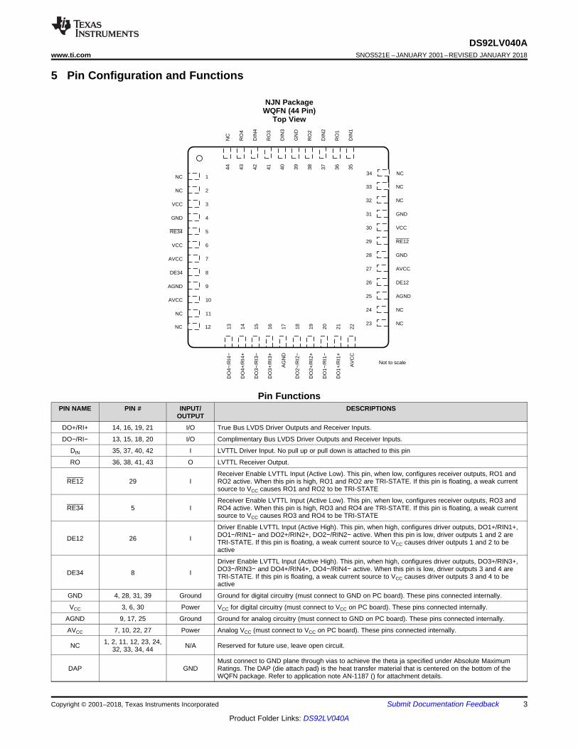
6.5 DC Electrical Characteristics (1)
Over recommended operating supply voltage and temperature ranges unless otherwise specified. (2) (3)
PARAMETER TEST CONDITIONS PIN MIN TYP MAX UNIT
VOD Output Differential Voltage
RL = 27Ω, Figure 1
DO+/RI+,DO−/RI−
200 300 460 mV
ΔVOD VOD Magnitude Change 5 27 mV
VOS Offset Voltage 1.1 1.3 1.5 V
ΔVOS Offset Magnitude Change 5 10 mV
VOHD Driver Output High Voltage RL = 27Ω 1.4 1.65 V
VOLD Driver Output Low Voltage RL = 27Ω 0.95 1.1 V
IOSDDriver Output Short CircuitCurrent
VOD = 0V, DE = VCC, Driver outputs shortedtogether |30| | 45| mA
VOHR Receiver Voltage Output High (4)
VID = +300 mV
IOH = −4 mA
ROUT
VCC−0.2 V
Inputs Open VCC−0.2 V
Inputs Terminated,RL = 27Ω VCC−0.2 V
VOLR Receiver Voltage Output Low IOL = 4.0 mA, VID = −300 mV 0.05 0.100 V
IOD Receiver Output Dynamic CurrentVID = 300mV, VOUT = VCC−1.0V −50 |33| mA
VID = −300mV, VOUT = 1.0V |36| 60 mA
VTH Input Threshold High (5)
DE = 0V, Over common mode range
DO+/RI+,DO−/RI−
−40 0 mV
VTL Input Threshold Low (5) −70 −40 mV
VCMR Receiver Common Mode Range |VID|/2 2.4 −|VID|/2 V
IIN Input CurrentDE = 0V, RE = 2.4V,VIN = +2.4V or 0V −20 ±1 +20 µA
VCC = 0V, VIN = +2.4V or 0V −20 ±1 +20 µA
VIH Minimum Input High Voltage
DIN, DE, RE
2.0 VCC V
VIL Maximum Input Low Voltage GND 0.8 V
IIH Input High Current VIN = VCC or 2.4V −20 ±2.5 +20 µA
IIL Input Low Current VIN = GND or 0.4V −20 ±2.5 +20 µA
VCL Input Diode Clamp Voltage ICLAMP = −18 mA −1.5 −0.8 V
ICCDPower Supply Current DriversEnabled, Receivers Disabled
No Load, DE = RE = VCC,DIN = VCC or GND
VCC
20 40 mA
ICCRPower Supply Current DriversDisabled, Receivers Enabled
DE = RE = 0V, VID = ±300mV 27 40 mA
ICCZPower Supply Current, Driversand Receivers TRI-STATE
DE = 0V; RE = VCC,DIN = VCC or GND 28 40 mA
ICCPower Supply Current, Driversand Receivers Enabled
DE = VCC; RE = 0V,DIN = VCC or GND,RL = 27Ω
70 100 mA
IOFF Power Off Leakage CurrentVCC = 0V or OPEN,DIN, DE, RE = 0V or OPEN,VAPPLIED = 3.6V (Port Pins)
DO+/RI+,DO−/RI− −20 +20 µA
COUTPUT Capacitance at Bus Pins DO+/RI+,DO−/RI− 5 pF
cOUTPUT Capacitance at ROUT ROUT 5 pF
6
DS92LV040ASNOS521E –JANUARY 2001–REVISED JANUARY 2018 www.ti.com
Product Folder Links: DS92LV040A
Submit Documentation Feedback Copyright © 2001–2018, Texas Instruments Incorporated
(1) Generator waveforms for all tests unless otherwise specified: f = 25 MHz, ZO = 50 Ω, tr, tf = <1 ns (0%–100%). To ensure fastestpropagation delay and minimum skew, data input edge rates should be equal to or faster than 1 ns/V; control signals equal to or fasterthan 3ns/V. In general, the faster the input edge rate, the better the AC performance.
(2) CL includes probe and fixture capacitance.(3) Propagation delays, transition times, and receiver threshold are ensured by design and characterization.(4) tSKD1 |tPHLD–tPLHD| is the worst case pulse skew (measure of duty cycle) over recommended operation conditions.(5) Chip to Chip skew is the difference in differential propagation delay between any channels of any devices, either edge.
6.6 AC Electrical CharacteristicsOver recommended operating supply voltage and temperature ranges unless otherwise specified. (1)
PARAMETER TEST CONDITIONS (2) MIN TYP MAX UNIT
DIFFERENTIAL DRIVER TIMING REQUIREMENTS
tPHLD Differential Prop. Delay High to Low (3)
RL = 27Ω,Figure 2, Figure 3,CL = 10 pF
1 1.5 2.3 ns
tPLHD Differential Prop. Delay Low to High (3) 1 1.5 2.3 ns
tSKD1 Differential Skew |tPHLD–tPLHD| (duty cycle) (4) (3) 80 160 ps
tCCSK Channel to Channel Skew (all 4 channels) (3) (5) 220 400 ps
tTLH Transition Time Low to High (20% to 80%) 0.4 0.75 1.3 ns
tTHL Transition Time High to Low (80% to 20%) 0.4 0.75 1.3 ns
tPHZ Disable Time High to ZRL = 27Ω,Figure 4, Figure 5,CL = 10 pF
5 10 ns
tPLZ Disable Time Low to Z 5 10 ns
tPZH Enable Time Z to High 5 10 ns
tPZL Enable Time Z to Low 5 10 ns
fMAXD Ensured operation per data sheet up to the Min. Duty Cycle45/55%,Transition time ≤ 25% of period (3) 85 125 MHz
DIFFERENTIAL RECEIVER TIMING REQUIREMENTS
tPHLDR Differential Prop. Delay High to Low (3)
Figure 6, Figure 7,CL = 15 pF
1.6 2.4 3.2 ns
tPLHDR Differential Prop Delay Low to High (3) 1.6 2.4 3.2 ns
tSDK1R Differential Skew |tPHLD–tPLHD| (duty cycle) (4) (3) 85 160 ps
tCCSKR Channel to Channel Skew (all 4 channels) (3) (5) 140 300 ps
tTLHR Transition Time Low to High (10% to 90%) (3) 0.85 1.25 2 ns
tTHLR Transition Time High to Low (90% to 10%) (3) 0.85 1.03 2 ns
tPHZ Disable Time High to ZRL = 500Ω,Figure 8, Figure 9,CL = 15 pF
3 10 ns
tPLZ Disable Time Low to Z 3 10 ns
tPZH Enable Time Z to High 3 10 ns
tPZL Enable Time Z to Low 3 10 ns
fMAXREnsured operation per data sheet up to the Min. Duty Cycle45/55%,Transition time ≤ 25% of period (3) 85 125 MHz
7 Parameter Measurement Information
7.1 Test Circuits and Timing Waveforms
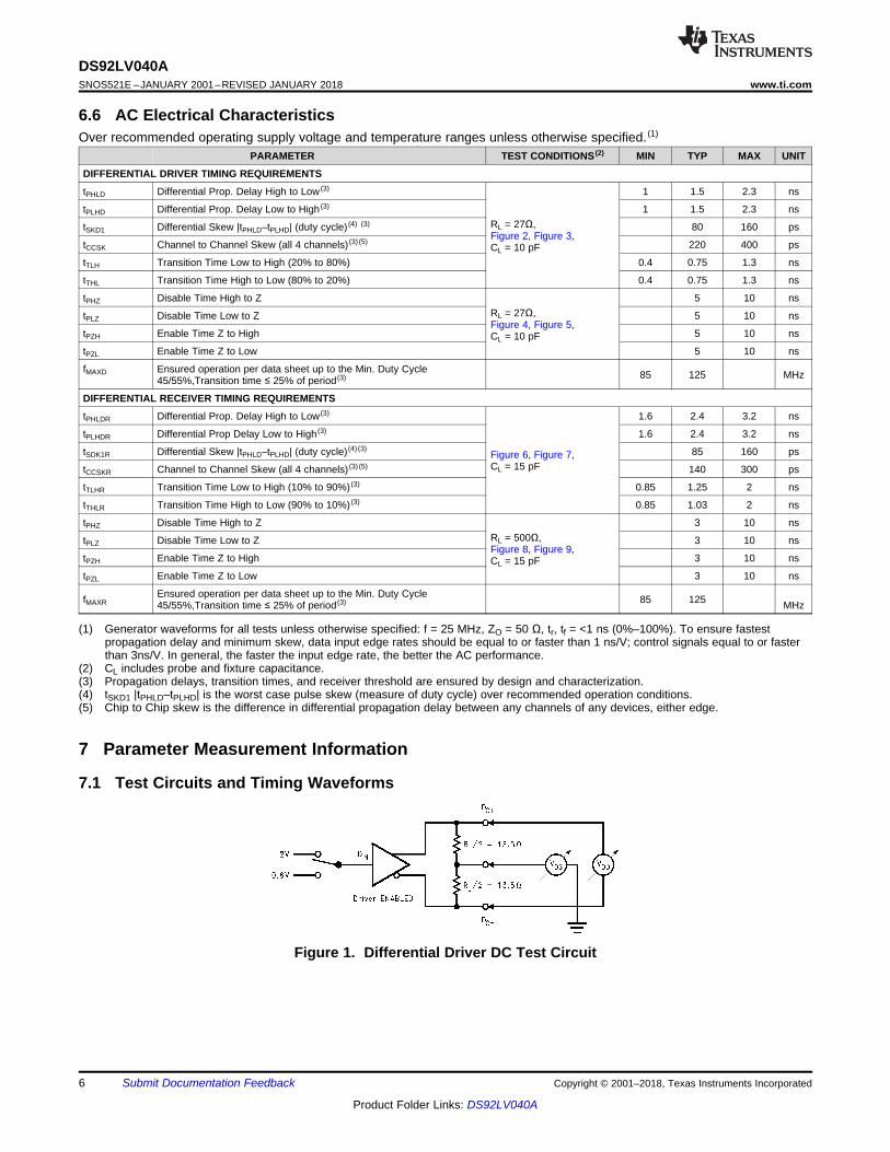
Figure 1. Differential Driver DC Test Circuit
7
DS92LV040Awww.ti.com SNOS521E –JANUARY 2001–REVISED JANUARY 2018
Product Folder Links: DS92LV040A
Submit Documentation FeedbackCopyright © 2001–2018, Texas Instruments Incorporated
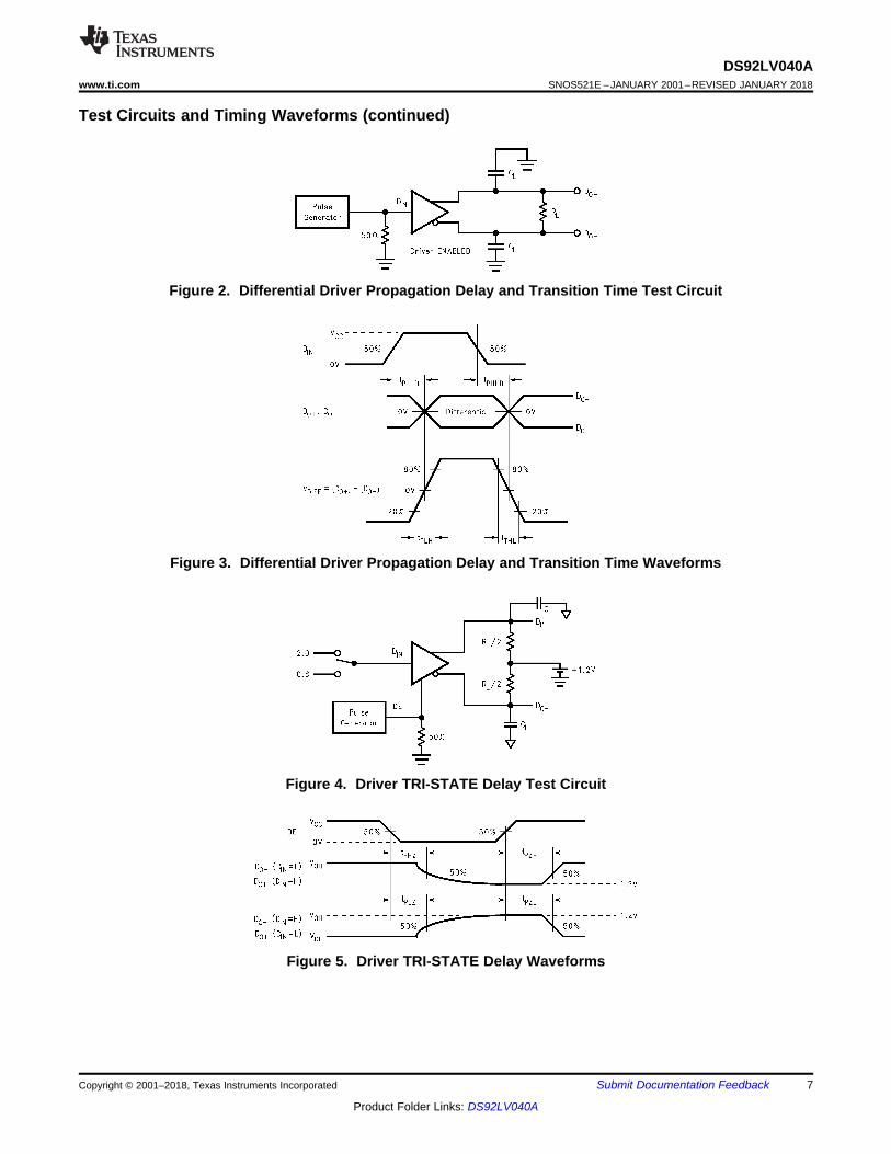
Test Circuits and Timing Waveforms (continued)
Figure 2. Differential Driver Propagation Delay and Transition Time Test Circuit
Figure 3. Differential Driver Propagation Delay and Transition Time Waveforms
Figure 4. Driver TRI-STATE Delay Test Circuit
Figure 5. Driver TRI-STATE Delay Waveforms
8
DS92LV040ASNOS521E –JANUARY 2001–REVISED JANUARY 2018 www.ti.com
Product Folder Links: DS92LV040A
Submit Documentation Feedback Copyright © 2001–2018, Texas Instruments Incorporated
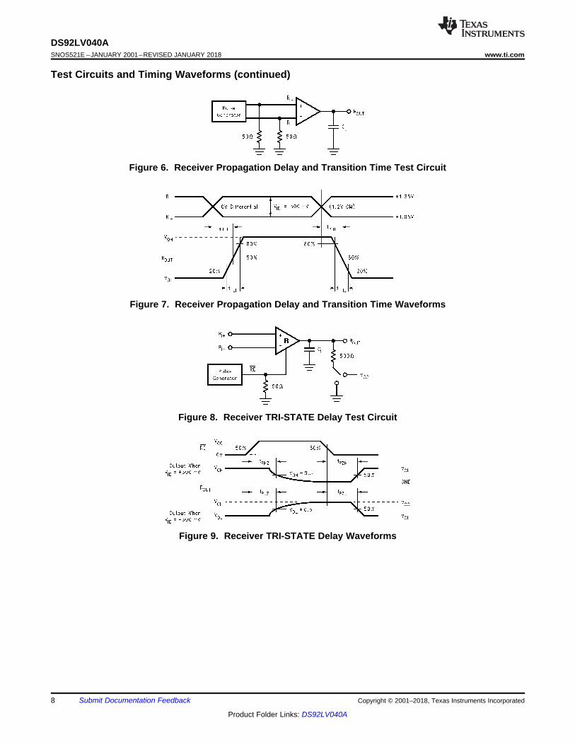
Test Circuits and Timing Waveforms (continued)
Figure 6. Receiver Propagation Delay and Transition Time Test Circuit
Figure 7. Receiver Propagation Delay and Transition Time Waveforms
Figure 8. Receiver TRI-STATE Delay Test Circuit
Figure 9. Receiver TRI-STATE Delay Waveforms
Copyright © 2018, Texas Instruments Incorporated
DIN1
DE1
RO1
DIN2
RO2
DIN3
DE2
RO3
DIN4
RO4
RE1
RE2
DO1+/RI1+
DO1-/RI1-
DO2+/RI2+
DO2-/RI2-
DO3+/RI3+
DO3-/RI3-
DO4+/RI4+
DO4-/RI4-
9
DS92LV040Awww.ti.com SNOS521E –JANUARY 2001–REVISED JANUARY 2018
Product Folder Links: DS92LV040A
Submit Documentation FeedbackCopyright © 2001–2018, Texas Instruments Incorporated
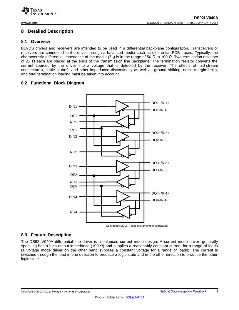
8 Detailed Description
8.1 OverviewBLVDS drivers and receivers are intended to be used in a differential backplane configuration. Transceivers orreceivers are connected to the driver through a balanced media such as differential PCB traces. Typically, thecharacteristic differential impedance of the media (ZO) is in the range of 50 Ω to 100 Ω. Two termination resistorsof ZO Ω each are placed at the ends of the transmission line backplane. The termination resistor converts thecurrent sourced by the driver into a voltage that is detected by the receiver. The effects of mid-streamconnector(s), cable stub(s), and other impedance discontinuity as well as ground shifting, noise margin limits,and total termination loading must be taken into account.
8.2 Functional Block Diagram
8.3 Feature DescriptionThe DS92LV040A differential line driver is a balanced current mode design. A current mode driver, generallyspeaking has a high output impedance (100 Ω) and supplies a reasonably constant current for a range of loads(a voltage mode driver on the other hand supplies a constant voltage for a range of loads). The current isswitched through the load in one direction to produce a logic state and in the other direction to produce the otherlogic state.

10
DS92LV040ASNOS521E –JANUARY 2001–REVISED JANUARY 2018 www.ti.com
Product Folder Links: DS92LV040A
Submit Documentation Feedback Copyright © 2001–2018, Texas Instruments Incorporated
Feature Description (continued)The current mode driver provides substantial benefits over voltage mode drivers, such as an RS-422 driver. Itsquiescent current remains relatively flat versus switching frequency. Whereas the RS-422 voltage mode driverincreases exponentially in most case between 20 MHz–50 MHz. This is due to the overlap current that flowsbetween the rails of the device when the internal gates switch. Whereas the current mode driver switches a fixedcurrent between its output without any substantial overlap current. This is similar to some ECL and PECLdevices, but without the heavy static ICC requirements of the ECL/PECL designs. LVDS requires 80% lesscurrent than similar PECL devices. AC specifications for the driver are a tenfold improvement over other existingRS-422 drivers. The TRI-STATE function allows the driver outputs to be disabled, thus obtaining an even lowerpower state when the transmission of data is not required.
8.4 Device Functional Modes
Table 1. Functional TableMODE SELECTED DE RE
DRIVER MODE H HRECEIVER MODE L LTRI-STATE MODE L H
LOOP BACK MODE H L
Table 2. Transmitter ModeINPUTS OUTPUTS
DE DIN DO+ DO−H L L HH H H LH 0.8V< DIN <2.0V X XL X Z Z
Table 3. Receiver ModeINPUTS OUTPUT
RE (RI+) – (RI−)L L (< −70 mV) LL H (> 0 mV) HL −70 mV < VID < 0 mV XH X Z
Copyright © 2018, Texas Instruments Incorporated
RT
ROUT
DIN
DERE
D0+
D0-
RI+
RI-
+
-
RT
ROUT
DIN
DERE
D0+
D0-
RI+
RI-
+
-
11
DS92LV040Awww.ti.com SNOS521E –JANUARY 2001–REVISED JANUARY 2018
Product Folder Links: DS92LV040A
Submit Documentation FeedbackCopyright © 2001–2018, Texas Instruments Incorporated
9 Application and Implementation
NOTEInformation in the following applications sections is not part of the TI componentspecification, and TI does not warrant its accuracy or completeness. TI’s customers areresponsible for determining suitability of components for their purposes. Customers shouldvalidate and test their design implementation to confirm system functionality.
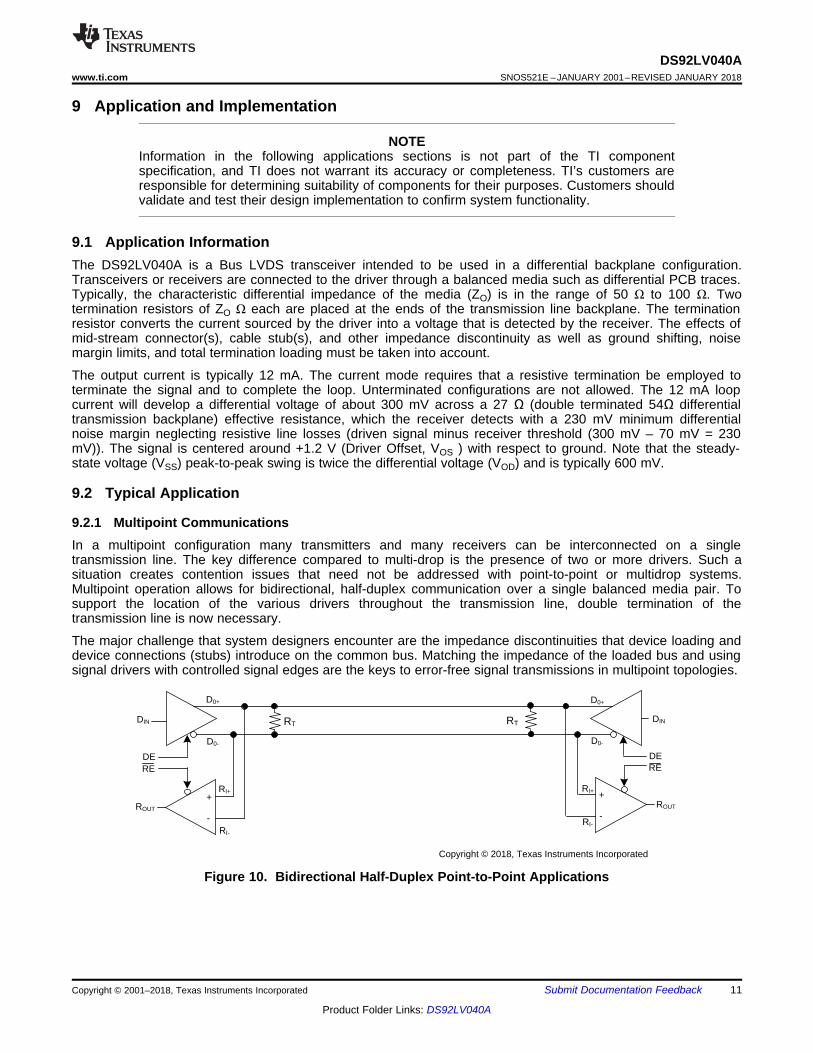
9.1 Application InformationThe DS92LV040A is a Bus LVDS transceiver intended to be used in a differential backplane configuration.Transceivers or receivers are connected to the driver through a balanced media such as differential PCB traces.Typically, the characteristic differential impedance of the media (ZO) is in the range of 50 Ω to 100 Ω. Twotermination resistors of ZO Ω each are placed at the ends of the transmission line backplane. The terminationresistor converts the current sourced by the driver into a voltage that is detected by the receiver. The effects ofmid-stream connector(s), cable stub(s), and other impedance discontinuity as well as ground shifting, noisemargin limits, and total termination loading must be taken into account.
The output current is typically 12 mA. The current mode requires that a resistive termination be employed toterminate the signal and to complete the loop. Unterminated configurations are not allowed. The 12 mA loopcurrent will develop a differential voltage of about 300 mV across a 27 Ω (double terminated 54Ω differentialtransmission backplane) effective resistance, which the receiver detects with a 230 mV minimum differentialnoise margin neglecting resistive line losses (driven signal minus receiver threshold (300 mV – 70 mV = 230mV)). The signal is centered around +1.2 V (Driver Offset, VOS ) with respect to ground. Note that the steady-state voltage (VSS) peak-to-peak swing is twice the differential voltage (VOD) and is typically 600 mV.
9.2 Typical Application
9.2.1 Multipoint CommunicationsIn a multipoint configuration many transmitters and many receivers can be interconnected on a singletransmission line. The key difference compared to multi-drop is the presence of two or more drivers. Such asituation creates contention issues that need not be addressed with point-to-point or multidrop systems.Multipoint operation allows for bidirectional, half-duplex communication over a single balanced media pair. Tosupport the location of the various drivers throughout the transmission line, double termination of thetransmission line is now necessary.
The major challenge that system designers encounter are the impedance discontinuities that device loading anddevice connections (stubs) introduce on the common bus. Matching the impedance of the loaded bus and usingsignal drivers with controlled signal edges are the keys to error-free signal transmissions in multipoint topologies.
Figure 10. Bidirectional Half-Duplex Point-to-Point Applications

Copyright © 2018, Texas Instruments Incorporated
RTRT
DIN / ROUTDIN / ROUT DIN / ROUT DIN / ROUT
DIN / ROUT DIN / ROUT DIN / ROUT
12
DS92LV040ASNOS521E –JANUARY 2001–REVISED JANUARY 2018 www.ti.com
Product Folder Links: DS92LV040A
Submit Documentation Feedback Copyright © 2001–2018, Texas Instruments Incorporated
Typical Application (continued)
Figure 11. Multi-Point Bus Applications
9.2.2 Design RequirementsFor this design example, use the parameters listed in Table 4.
Table 4. Design ParametersPARAMETERS VALUES
Driver supply voltage 3 to 3.6 VDriver input voltage 0.8 to 3.3 VDriver signaling rate DC to 200 Mbps
Interconnect characteristic impedance 100 Ω
Termination resistance (differential) 100 Ω
Number of receiver nodes 2 to 32Receiver supply voltage 3 to 3.6 VReceiver input voltage 0 to (VCC – 0.8) VReceiver signaling rate DC to 200 Mbps
Ground shift between driver and receiver ±1 V
9.2.3 Detailed Design Procedure
9.2.3.1 Supply VoltageThe DS92LV040A is operated from a single supply. The device can support operations with a supply as low as3 V and as high as 3.6 V.
9.2.3.2 Supply Bypass CapacitanceBypass capacitors play a key role in power distribution circuitry. At low frequencies, power supply offers very low-impedance paths between its terminals. However, as higher frequency currents propagate through power traces,the source is often incapable of maintaining a low-impedance path to ground. Bypass capacitors are used toaddress this shortcoming. Usually, large bypass capacitors (10 μF to 1000 μF) at the board level do a good jobup into the kHz range. Due to their size and length of their leads, large capacitors tend to have large inductancevalues at the switching frequencies. To solve this problem, smaller capacitors (in the nF to μF range) must beinstalled locally next to the integrated circuit.

13
DS92LV040Awww.ti.com SNOS521E –JANUARY 2001–REVISED JANUARY 2018
Product Folder Links: DS92LV040A
Submit Documentation FeedbackCopyright © 2001–2018, Texas Instruments Incorporated
9.2.3.3 Termination ResistorsMultipoint LVDS communication channel employs a current source driving a transmission line which is terminatedwith two resistive loads. These loads serve to convert the transmitted current into a voltage at the receiver input.To ensure good signal integrity, the termination resistors should be matched to the characteristic impedance ofthe transmission line. The designer should ensure that the termination resistors are within 10% of the nominalmedia characteristic impedance. If the transmission line is targeted for 100-Ω impedance, the terminationresistors should be between 90 Ω and 110 Ω. The line termination resistors are typically placed at the ends of thetransmission line.
9.2.3.4 Interconnecting MediaThe backplane and connectors should have a matched differential impedance. Use controlled impedance traceswhich match the differential impedance of your transmission medium (ie. backplane or cable) and terminationresistor(s). Run the differential pair trace lines as close together as possible as soon as they leave the IC. Thishelps eliminate reflections and ensure noise is coupled as common-mode. In fact, it has been determined thatdifferential signals which are 1 mm apart radiate far less noise than traces 3 mm apart since magnetic fieldcancellation is much better with the closer traces. Plus, noise induced on the differential lines is much more likelyto appear as common-mode which is rejected by the receiver. Match electrical lengths between traces to reduceskew. Skew between the signals of a pair means a phase difference between signals which destroys themagnetic field cancellation benefits of differential signals and EMI will result.
Stub lengths should be kept to a minimum. The typical transition time of the DS92LV040A Bus LVDS output is0.75 ns (20% to 80%). The extrapolated 100 percent time is 0.75/0.6 or 1.25 ns. For a general approximation, ifthe electrical length of a trace is greater than 1/5 of the transition edge, then the trace is considered atransmission line. For example, 1.25 ns/5 is 250 picoseconds. Let velocity equal 160 ps per inch for a typicalloaded backplane. Then maximum stub length is 250 ps/160 ps/in or 1.56 inches. To determine the maximumstub for the backplane, determine the propagation velocity for the actual conditions (refer to application notes AN905 and AN 808)
10 Power Supply RecommendationsThe driver and receivers in this data sheet are designed to operate from a single power supply. Both drivers andreceivers operate with supply voltages in the range of 3 V to 3.6 V. In a typical application, a driver and areceiver may be on separate boards, or even separate equipment. In these cases, separate supplies would beused at each location. The expected ground potential difference between the driver power supply and thereceiver power supply would be less than ±1 V. Board level and local device level bypass capacitance should beused and are covered Supply Bypass Capacitance.
14
DS92LV040ASNOS521E –JANUARY 2001–REVISED JANUARY 2018 www.ti.com
Product Folder Links: DS92LV040A
Submit Documentation Feedback Copyright © 2001–2018, Texas Instruments Incorporated
(1) Howard Johnson & Martin Graham.1993. High Speed Digital Design – A Handbook of Black Magic. Prentice Hall PRT. ISBN number013395724.
(2) Mark I. Montrose. 1996. Printed Circuit Board Design Techniques for EMC Compliance. IEEE Press. ISBN number 0780311310.(3) Clyde F. Coombs, Jr. Ed, Printed Circuits Handbook, McGraw Hill, ISBN number 0070127549.
11 Layout
11.1 Layout Guidelines
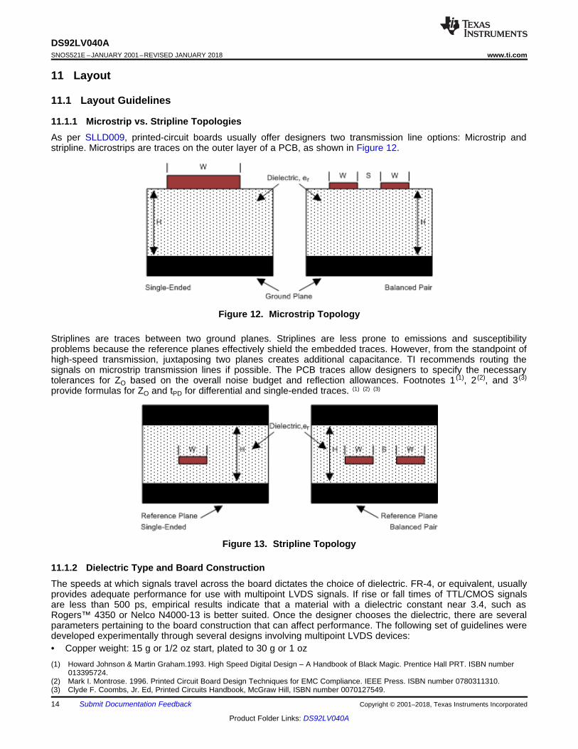
11.1.1 Microstrip vs. Stripline TopologiesAs per SLLD009, printed-circuit boards usually offer designers two transmission line options: Microstrip andstripline. Microstrips are traces on the outer layer of a PCB, as shown in Figure 12.
Figure 12. Microstrip Topology
Striplines are traces between two ground planes. Striplines are less prone to emissions and susceptibilityproblems because the reference planes effectively shield the embedded traces. However, from the standpoint ofhigh-speed transmission, juxtaposing two planes creates additional capacitance. TI recommends routing thesignals on microstrip transmission lines if possible. The PCB traces allow designers to specify the necessarytolerances for ZO based on the overall noise budget and reflection allowances. Footnotes 1 (1), 2 (2), and 3 (3)
provide formulas for ZO and tPD for differential and single-ended traces. (1) (2) (3)
Figure 13. Stripline Topology
11.1.2 Dielectric Type and Board ConstructionThe speeds at which signals travel across the board dictates the choice of dielectric. FR-4, or equivalent, usuallyprovides adequate performance for use with multipoint LVDS signals. If rise or fall times of TTL/CMOS signalsare less than 500 ps, empirical results indicate that a material with a dielectric constant near 3.4, such asRogers™ 4350 or Nelco N4000-13 is better suited. Once the designer chooses the dielectric, there are severalparameters pertaining to the board construction that can affect performance. The following set of guidelines weredeveloped experimentally through several designs involving multipoint LVDS devices:• Copper weight: 15 g or 1/2 oz start, plated to 30 g or 1 oz
Layer 4: Routed Plane (TTL Signals)
Layer 3: Power Plane
Layer 2: Ground Plane
Layer 1: Routed Plane (MLVDS Signals)
Layer 4: Ground Plane
Layer 5: Ground Plane
Layer 4: Routed Plane (TTL/CMOS Signals)
Layer 3: Power Plane
Layer 2: Ground Plane
Layer 1: Routed Plane (MLVDS Signals)
15
DS92LV040Awww.ti.com SNOS521E –JANUARY 2001–REVISED JANUARY 2018
Product Folder Links: DS92LV040A
Submit Documentation FeedbackCopyright © 2001–2018, Texas Instruments Incorporated
Layout Guidelines (continued)• All exposed circuitry should be solder-plated (60/40) to 7.62 μm or 0.0003 in (minimum).• Copper plating should be 25.4 μm or 0.001 in (minimum) in plated-through-holes.• Solder mask over bare copper with solder hot-air leveling
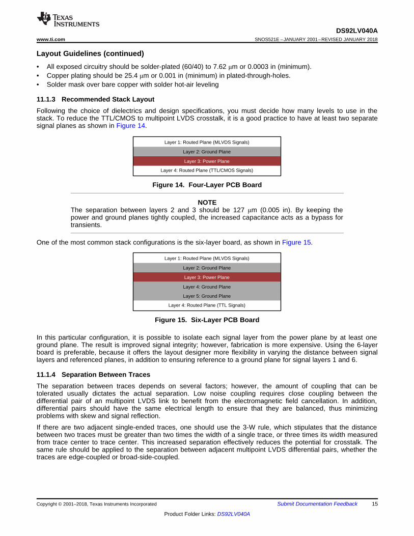
11.1.3 Recommended Stack LayoutFollowing the choice of dielectrics and design specifications, you must decide how many levels to use in thestack. To reduce the TTL/CMOS to multipoint LVDS crosstalk, it is a good practice to have at least two separatesignal planes as shown in Figure 14.
Figure 14. Four-Layer PCB Board
NOTEThe separation between layers 2 and 3 should be 127 μm (0.005 in). By keeping thepower and ground planes tightly coupled, the increased capacitance acts as a bypass fortransients.
One of the most common stack configurations is the six-layer board, as shown in Figure 15.
Figure 15. Six-Layer PCB Board
In this particular configuration, it is possible to isolate each signal layer from the power plane by at least oneground plane. The result is improved signal integrity; however, fabrication is more expensive. Using the 6-layerboard is preferable, because it offers the layout designer more flexibility in varying the distance between signallayers and referenced planes, in addition to ensuring reference to a ground plane for signal layers 1 and 6.
11.1.4 Separation Between TracesThe separation between traces depends on several factors; however, the amount of coupling that can betolerated usually dictates the actual separation. Low noise coupling requires close coupling between thedifferential pair of an multipoint LVDS link to benefit from the electromagnetic field cancellation. In addition,differential pairs should have the same electrical length to ensure that they are balanced, thus minimizingproblems with skew and signal reflection.
If there are two adjacent single-ended traces, one should use the 3-W rule, which stipulates that the distancebetween two traces must be greater than two times the width of a single trace, or three times its width measuredfrom trace center to trace center. This increased separation effectively reduces the potential for crosstalk. Thesame rule should be applied to the separation between adjacent multipoint LVDS differential pairs, whether thetraces are edge-coupled or broad-side-coupled.
Boa
rd th
ickn
ess
appr
oxim
atel
y 10
0 m
il
2 mil
Typical 12-Layer PCB
4 mil
4 mil
6 mil
6 mil
VCCVia
GNDVia
TOP signal layer + GND fill
VDD 1 planeGND planeSignal layer
Buried capacitor>
Signal layerGND plane
VDD 2 planeBOTTOM signal layer + GND fill
Buried capacitor>
GND plane
Signal layers
VCC plane
t2 W
W
W
W
Minimum spacing asdefined by PCB vendor
MLVDSPair
TTL/CMOSTrace
Differential Traces
Single-Ended Traces
S =
16
DS92LV040ASNOS521E –JANUARY 2001–REVISED JANUARY 2018 www.ti.com
Product Folder Links: DS92LV040A
Submit Documentation Feedback Copyright © 2001–2018, Texas Instruments Incorporated
Layout Guidelines (continued)
Figure 16. 3-W Rule for Single-Ended and Differential Traces (Top View)
You should exercise caution when using autorouters, because they do not always account for all factors affectingcrosstalk and signal reflection. For instance, it is best to avoid sharp 90° turns to prevent discontinuities in thesignal path. Using successive 45° turns tends to minimize reflections.
11.1.5 Crosstalk and Ground Bounce MinimizationTo reduce crosstalk, it is important to provide a return path to high-frequency currents that is as close as possibleto its originating trace. A ground plane usually achieves this. Because the returning currents always choose thepath of lowest inductance, they are most likely to return directly under the original trace, thus minimizingcrosstalk. Lowering the area of the current loop lowers the potential for crosstalk. Traces kept as short aspossible with an uninterrupted ground plane running beneath them emit the minimum amount of electromagneticfield strength. Discontinuities in the ground plane increase the return path inductance and should be avoided.
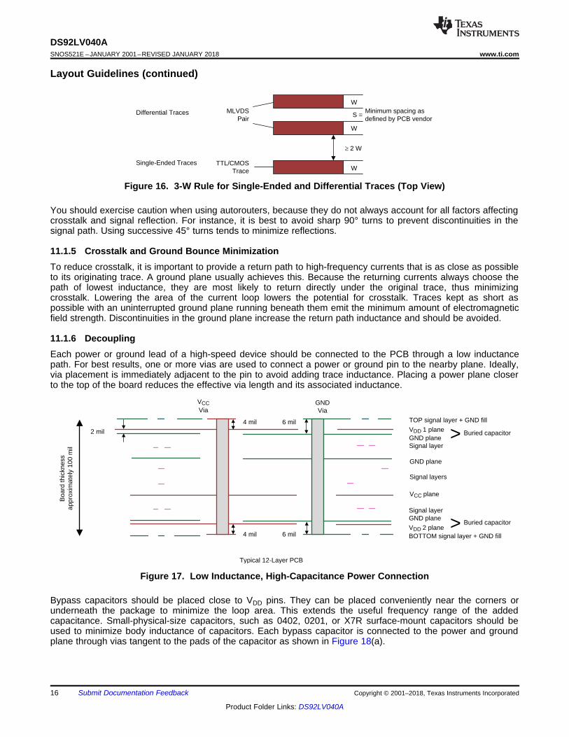
11.1.6 DecouplingEach power or ground lead of a high-speed device should be connected to the PCB through a low inductancepath. For best results, one or more vias are used to connect a power or ground pin to the nearby plane. Ideally,via placement is immediately adjacent to the pin to avoid adding trace inductance. Placing a power plane closerto the top of the board reduces the effective via length and its associated inductance.
Figure 17. Low Inductance, High-Capacitance Power Connection
Bypass capacitors should be placed close to VDD pins. They can be placed conveniently near the corners orunderneath the package to minimize the loop area. This extends the useful frequency range of the addedcapacitance. Small-physical-size capacitors, such as 0402, 0201, or X7R surface-mount capacitors should beused to minimize body inductance of capacitors. Each bypass capacitor is connected to the power and groundplane through vias tangent to the pads of the capacitor as shown in Figure 18(a).

Layer 6
Layer 1
0402
VDD
IN±
IN+
0402
17
DS92LV040Awww.ti.com SNOS521E –JANUARY 2001–REVISED JANUARY 2018
Product Folder Links: DS92LV040A
Submit Documentation FeedbackCopyright © 2001–2018, Texas Instruments Incorporated
Layout Guidelines (continued)An X7R surface-mount capacitor of size 0402 has about 0.5 nH of body inductance. At frequencies above 30MHz or so, X7R capacitors behave as low-impedance inductors. To extend the operating frequency range to afew hundred MHz, an array of different capacitor values like 100 pF, 1 nF, 0.03 μF, and 0.1 μF are commonlyused in parallel. The most effective bypass capacitor can be built using sandwiched layers of power and groundat a separation of 2 to 3 mils. With a 2-mil FR4 dielectric, there is approximately 500 pF per square inch of PCB.Many high-speed devices provide a low-inductance GND connection on the backside of the package. This centerpad must be connected to a ground plane through an array of vias. The via array reduces the effectiveinductance to ground and enhances the thermal performance of the small Surface Mount Technology (SMT)package. Placing vias around the perimeter of the pad connection ensures proper heat spreading and the lowestpossible die temperature. Placing high-performance devices on opposing sides of the PCB using two GNDplanes creates multiple paths for heat transfer. Often thermal PCB issues are the result of one device addingheat to another, resulting in a very high local temperature. Multiple paths for heat transfer minimize thispossibility. In many cases the GND pad makes the optimal decoupling layout impossible to achieve due toinsufficient pad-to-pad spacing as shown in Figure 18(b). When this occurs, placing the decoupling capacitor onthe backside of the board keeps the extra inductance to a minimum. It is important to place the VDD via as closeto the device pin as possible while still allowing for sufficient solder mask coverage. If the via is left open, soldermay flow from the pad and into the via barrel. This results in a poor solder connection.
(a) (b)
Figure 18. Typical Decoupling Capacitor Layouts
11.2 Layout ExampleAt least two or three times the width of an individual trace should separate single-ended traces and differentialpairs to minimize the potential for crosstalk. Single-ended traces that run in parallel for less than the wavelengthof the rise or fall times usually have negligible crosstalk. Increase the spacing between signal paths for longparallel runs to reduce crosstalk. Boards with limited real estate can benefit from the staggered trace layout, asshown in Figure 19.
Figure 19. Staggered Trace Layout

Signal Trace
Uninterrupted Ground Plane
Signal Trace
Uninterrupted Ground Plane
Signal Via
Ground Via
18
DS92LV040ASNOS521E –JANUARY 2001–REVISED JANUARY 2018 www.ti.com
Product Folder Links: DS92LV040A
Submit Documentation Feedback Copyright © 2001–2018, Texas Instruments Incorporated
Layout Example (continued)This configuration lays out alternating signal traces on different layers; thus, the horizontal separation betweentraces can be less than 2 or 3 times the width of individual traces. To ensure continuity in the ground signal path,TI recommends having an adjacent ground via for every signal via, as shown in Figure 20. Note that vias createadditional capacitance. For example, a typical via has a lumped capacitance effect of 1/2 pF to 1 pF in FR4.
Figure 20. Ground Via Location (Side View)
Short and low-impedance connection of the device ground pins to the PCB ground plane reduces groundbounce. Holes and cutouts in the ground planes can adversely affect current return paths if they creatediscontinuities that increase returning current loop areas.
To minimize EMI problems, TI recommends avoiding discontinuities below a trace (for example, holes, slits, andso on) and keeping traces as short as possible. Zoning the board wisely by placing all similar functions in thesame area, as opposed to mixing them together, helps reduce susceptibility issues.

19
DS92LV040Awww.ti.com SNOS521E –JANUARY 2001–REVISED JANUARY 2018
Product Folder Links: DS92LV040A
Submit Documentation FeedbackCopyright © 2001–2018, Texas Instruments Incorporated
12 Device and Documentation Support
12.1 Documentation Support
12.1.1 Related DocumentationGeneral application guidelines and hints may be found in the following application notes: ), A).
For related documentation see the following:• AN-808 (SNLA028)• AN-977 (SNLA166• AN-971 (SNLA165)• AN-903 (SNLA034
12.2 Receiving Notification of Documentation UpdatesTo receive notification of documentation updates, navigate to the device product folder on ti.com. In the upperright corner, click on Alert me to register and receive a weekly digest of any product information that haschanged. For change details, review the revision history included in any revised document.
12.3 Community ResourcesThe following links connect to TI community resources. Linked contents are provided "AS IS" by the respectivecontributors. They do not constitute TI specifications and do not necessarily reflect TI's views; see TI's Terms ofUse.
TI E2E™ Online Community TI's Engineer-to-Engineer (E2E) Community. Created to foster collaborationamong engineers. At e2e.ti.com, you can ask questions, share knowledge, explore ideas and helpsolve problems with fellow engineers.
Design Support TI's Design Support Quickly find helpful E2E forums along with design support tools andcontact information for technical support.
12.4 TrademarksE2E is a trademark of Texas Instruments.Rogers is a trademark of Rogers Corporation.All other trademarks are the property of their respective owners.
12.5 Electrostatic Discharge CautionThis integrated circuit can be damaged by ESD. Texas Instruments recommends that all integrated circuits be handled withappropriate precautions. Failure to observe proper handling and installation procedures can cause damage.
ESD damage can range from subtle performance degradation to complete device failure. Precision integrated circuits may be moresusceptible to damage because very small parametric changes could cause the device not to meet its published specifications.
12.6 GlossarySLYZ022 — TI Glossary.
This glossary lists and explains terms, acronyms, and definitions.
13 Mechanical, Packaging, and Orderable InformationThe following pages include mechanical, packaging, and orderable information. This information is the mostcurrent data available for the designated devices. This data is subject to change without notice and revision ofthis document. For browser-based versions of this data sheet, refer to the left-hand navigation.
PACKAGE OPTION ADDENDUM
www.ti.com 22-Dec-2017
Addendum-Page 1
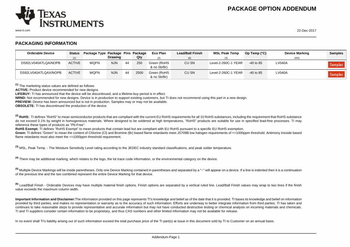
PACKAGING INFORMATION
Orderable Device Status(1)
Package Type PackageDrawing
Pins PackageQty
Eco Plan(2)
Lead/Ball Finish(6)
MSL Peak Temp(3)
Op Temp (°C) Device Marking(4/5)
Samples
DS92LV040ATLQA/NOPB ACTIVE WQFN NJN 44 250 Green (RoHS& no Sb/Br)
CU SN Level-2-260C-1 YEAR -40 to 85 LV040A
DS92LV040ATLQAX/NOPB ACTIVE WQFN NJN 44 2500 Green (RoHS& no Sb/Br)
CU SN Level-2-260C-1 YEAR -40 to 85 LV040A
(1) The marketing status values are defined as follows:ACTIVE: Product device recommended for new designs.LIFEBUY: TI has announced that the device will be discontinued, and a lifetime-buy period is in effect.NRND: Not recommended for new designs. Device is in production to support existing customers, but TI does not recommend using this part in a new design.PREVIEW: Device has been announced but is not in production. Samples may or may not be available.OBSOLETE: TI has discontinued the production of the device.
(2) RoHS: TI defines "RoHS" to mean semiconductor products that are compliant with the current EU RoHS requirements for all 10 RoHS substances, including the requirement that RoHS substancedo not exceed 0.1% by weight in homogeneous materials. Where designed to be soldered at high temperatures, "RoHS" products are suitable for use in specified lead-free processes. TI mayreference these types of products as "Pb-Free".RoHS Exempt: TI defines "RoHS Exempt" to mean products that contain lead but are compliant with EU RoHS pursuant to a specific EU RoHS exemption.Green: TI defines "Green" to mean the content of Chlorine (Cl) and Bromine (Br) based flame retardants meet JS709B low halogen requirements of <=1000ppm threshold. Antimony trioxide basedflame retardants must also meet the <=1000ppm threshold requirement.
(3) MSL, Peak Temp. - The Moisture Sensitivity Level rating according to the JEDEC industry standard classifications, and peak solder temperature.
(4) There may be additional marking, which relates to the logo, the lot trace code information, or the environmental category on the device.
(5) Multiple Device Markings will be inside parentheses. Only one Device Marking contained in parentheses and separated by a "~" will appear on a device. If a line is indented then it is a continuationof the previous line and the two combined represent the entire Device Marking for that device.
(6) Lead/Ball Finish - Orderable Devices may have multiple material finish options. Finish options are separated by a vertical ruled line. Lead/Ball Finish values may wrap to two lines if the finishvalue exceeds the maximum column width.
Important Information and Disclaimer:The information provided on this page represents TI's knowledge and belief as of the date that it is provided. TI bases its knowledge and belief on informationprovided by third parties, and makes no representation or warranty as to the accuracy of such information. Efforts are underway to better integrate information from third parties. TI has taken andcontinues to take reasonable steps to provide representative and accurate information but may not have conducted destructive testing or chemical analysis on incoming materials and chemicals.TI and TI suppliers consider certain information to be proprietary, and thus CAS numbers and other limited information may not be available for release.
In no event shall TI's liability arising out of such information exceed the total purchase price of the TI part(s) at issue in this document sold by TI to Customer on an annual basis.
PACKAGE OPTION ADDENDUM
www.ti.com 22-Dec-2017
Addendum-Page 2
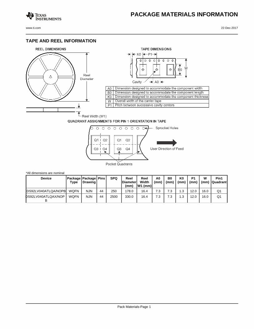
TAPE AND REEL INFORMATION
*All dimensions are nominal
Device PackageType
PackageDrawing
Pins SPQ ReelDiameter
(mm)
ReelWidth
W1 (mm)
A0(mm)
B0(mm)
K0(mm)
P1(mm)
W(mm)
Pin1Quadrant
DS92LV040ATLQA/NOPB WQFN NJN 44 250 178.0 16.4 7.3 7.3 1.3 12.0 16.0 Q1
DS92LV040ATLQAX/NOPB
WQFN NJN 44 2500 330.0 16.4 7.3 7.3 1.3 12.0 16.0 Q1
PACKAGE MATERIALS INFORMATION
www.ti.com 22-Dec-2017
Pack Materials-Page 1
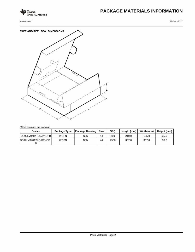
*All dimensions are nominal
Device Package Type Package Drawing Pins SPQ Length (mm) Width (mm) Height (mm)
DS92LV040ATLQA/NOPB WQFN NJN 44 250 210.0 185.0 35.0
DS92LV040ATLQAX/NOPB
WQFN NJN 44 2500 367.0 367.0 38.0
PACKAGE MATERIALS INFORMATION
www.ti.com 22-Dec-2017
Pack Materials-Page 2

MECHANICAL DATA
NJN0044A
www.ti.com
LQA44A (REV B)

IMPORTANT NOTICE
Texas Instruments Incorporated (TI) reserves the right to make corrections, enhancements, improvements and other changes to itssemiconductor products and services per JESD46, latest issue, and to discontinue any product or service per JESD48, latest issue. Buyersshould obtain the latest relevant information before placing orders and should verify that such information is current and complete.TI’s published terms of sale for semiconductor products (http://www.ti.com/sc/docs/stdterms.htm) apply to the sale of packaged integratedcircuit products that TI has qualified and released to market. Additional terms may apply to the use or sale of other types of TI products andservices.Reproduction of significant portions of TI information in TI data sheets is permissible only if reproduction is without alteration and isaccompanied by all associated warranties, conditions, limitations, and notices. TI is not responsible or liable for such reproduceddocumentation. Information of third parties may be subject to additional restrictions. Resale of TI products or services with statementsdifferent from or beyond the parameters stated by TI for that product or service voids all express and any implied warranties for theassociated TI product or service and is an unfair and deceptive business practice. TI is not responsible or liable for any such statements.Buyers and others who are developing systems that incorporate TI products (collectively, “Designers”) understand and agree that Designersremain responsible for using their independent analysis, evaluation and judgment in designing their applications and that Designers havefull and exclusive responsibility to assure the safety of Designers' applications and compliance of their applications (and of all TI productsused in or for Designers’ applications) with all applicable regulations, laws and other applicable requirements. Designer represents that, withrespect to their applications, Designer has all the necessary expertise to create and implement safeguards that (1) anticipate dangerousconsequences of failures, (2) monitor failures and their consequences, and (3) lessen the likelihood of failures that might cause harm andtake appropriate actions. Designer agrees that prior to using or distributing any applications that include TI products, Designer willthoroughly test such applications and the functionality of such TI products as used in such applications.TI’s provision of technical, application or other design advice, quality characterization, reliability data or other services or information,including, but not limited to, reference designs and materials relating to evaluation modules, (collectively, “TI Resources”) are intended toassist designers who are developing applications that incorporate TI products; by downloading, accessing or using TI Resources in anyway, Designer (individually or, if Designer is acting on behalf of a company, Designer’s company) agrees to use any particular TI Resourcesolely for this purpose and subject to the terms of this Notice.TI’s provision of TI Resources does not expand or otherwise alter TI’s applicable published warranties or warranty disclaimers for TIproducts, and no additional obligations or liabilities arise from TI providing such TI Resources. TI reserves the right to make corrections,enhancements, improvements and other changes to its TI Resources. TI has not conducted any testing other than that specificallydescribed in the published documentation for a particular TI Resource.Designer is authorized to use, copy and modify any individual TI Resource only in connection with the development of applications thatinclude the TI product(s) identified in such TI Resource. NO OTHER LICENSE, EXPRESS OR IMPLIED, BY ESTOPPEL OR OTHERWISETO ANY OTHER TI INTELLECTUAL PROPERTY RIGHT, AND NO LICENSE TO ANY TECHNOLOGY OR INTELLECTUAL PROPERTYRIGHT OF TI OR ANY THIRD PARTY IS GRANTED HEREIN, including but not limited to any patent right, copyright, mask work right, orother intellectual property right relating to any combination, machine, or process in which TI products or services are used. Informationregarding or referencing third-party products or services does not constitute a license to use such products or services, or a warranty orendorsement thereof. Use of TI Resources may require a license from a third party under the patents or other intellectual property of thethird party, or a license from TI under the patents or other intellectual property of TI.TI RESOURCES ARE PROVIDED “AS IS” AND WITH ALL FAULTS. TI DISCLAIMS ALL OTHER WARRANTIES ORREPRESENTATIONS, EXPRESS OR IMPLIED, REGARDING RESOURCES OR USE THEREOF, INCLUDING BUT NOT LIMITED TOACCURACY OR COMPLETENESS, TITLE, ANY EPIDEMIC FAILURE WARRANTY AND ANY IMPLIED WARRANTIES OFMERCHANTABILITY, FITNESS FOR A PARTICULAR PURPOSE, AND NON-INFRINGEMENT OF ANY THIRD PARTY INTELLECTUALPROPERTY RIGHTS. TI SHALL NOT BE LIABLE FOR AND SHALL NOT DEFEND OR INDEMNIFY DESIGNER AGAINST ANY CLAIM,INCLUDING BUT NOT LIMITED TO ANY INFRINGEMENT CLAIM THAT RELATES TO OR IS BASED ON ANY COMBINATION OFPRODUCTS EVEN IF DESCRIBED IN TI RESOURCES OR OTHERWISE. IN NO EVENT SHALL TI BE LIABLE FOR ANY ACTUAL,DIRECT, SPECIAL, COLLATERAL, INDIRECT, PUNITIVE, INCIDENTAL, CONSEQUENTIAL OR EXEMPLARY DAMAGES INCONNECTION WITH OR ARISING OUT OF TI RESOURCES OR USE THEREOF, AND REGARDLESS OF WHETHER TI HAS BEENADVISED OF THE POSSIBILITY OF SUCH DAMAGES.Unless TI has explicitly designated an individual product as meeting the requirements of a particular industry standard (e.g., ISO/TS 16949and ISO 26262), TI is not responsible for any failure to meet such industry standard requirements.Where TI specifically promotes products as facilitating functional safety or as compliant with industry functional safety standards, suchproducts are intended to help enable customers to design and create their own applications that meet applicable functional safety standardsand requirements. Using products in an application does not by itself establish any safety features in the application. Designers mustensure compliance with safety-related requirements and standards applicable to their applications. Designer may not use any TI products inlife-critical medical equipment unless authorized officers of the parties have executed a special contract specifically governing such use.Life-critical medical equipment is medical equipment where failure of such equipment would cause serious bodily injury or death (e.g., lifesupport, pacemakers, defibrillators, heart pumps, neurostimulators, and implantables). Such equipment includes, without limitation, allmedical devices identified by the U.S. Food and Drug Administration as Class III devices and equivalent classifications outside the U.S.TI may expressly designate certain products as completing a particular qualification (e.g., Q100, Military Grade, or Enhanced Product).Designers agree that it has the necessary expertise to select the product with the appropriate qualification designation for their applicationsand that proper product selection is at Designers’ own risk. Designers are solely responsible for compliance with all legal and regulatoryrequirements in connection with such selection.Designer will fully indemnify TI and its representatives against any damages, costs, losses, and/or liabilities arising out of Designer’s non-compliance with the terms and provisions of this Notice.
Mailing Address: Texas Instruments, Post Office Box 655303, Dallas, Texas 75265Copyright © 2018, Texas Instruments Incorporated