DS75176B/DS75176BT Multipoint RS-485/RS … Multipoint RS-485/RS-422Transceivers Check for Samples:...
14
DS75176B, DS75176BT www.ti.com SNLS381C – JULY 1998 – REVISED APRIL 2013 DS75176B/DS75176BT Multipoint RS-485/RS-422 Transceivers Check for Samples: DS75176B, DS75176BT 1FEATURES DESCRIPTION The DS75176B is a high speed differential TRI- 23• Meets EIA Standard RS485 for Multipoint Bus STATE ® bus/line transceiver designed to meet the Transmission and is Compatible with RS-422. requirements of EIA standard RS485 with extended • Small Outline (SOIC) Package Option Available common mode range (+12V to −7V), for multipoint for Minimum Board Space. data transmission. In addition, it is compatible with RS-422. • 22 ns Driver Propagation Delays. • Single +5V Supply. The driver and receiver outputs feature TRI-STATE capability, for the driver outputs over the entire • −7V to +12V Bus Common Mode Range common mode range of +12V to −7V. Bus contention Permits ±7V Ground Difference Between or fault situations that cause excessive power Devices on the Bus. dissipation within the device are handled by a thermal • Thermal Shutdown Protection. shutdown circuit, which forces the driver outputs into • High Impedance to Bus with Driver in TRI- the high impedance state. STATE or with Power Off, Over the Entire DC specifications are guaranteed over the 0 to 70°C Common Mode Range Allows the Unused temperature and 4.75V to 5.25V supply voltage Devices on the Bus to be Powered Down. range. • Pin Out Compatible with DS3695/A and SN75176A/B. • Combined Impedance of a Driver Output and Receiver Input is Less Than One RS485 Unit Load, Allowing up to 32 Transceivers on the Bus. • 70 mV Typical Receiver Hysteresis. Connection and Logic Diagram Figure 1. Top View See Package Number P0008E or D0008A These devices have limited built-in ESD protection. The leads should be shorted together or the device placed in conductive foam during storage or handling to prevent electrostatic damage to the MOS gates. 1 Please be aware that an important notice concerning availability, standard warranty, and use in critical applications of Texas Instruments semiconductor products and disclaimers thereto appears at the end of this data sheet. 2TRI-STATE is a registered trademark of Texas Instruments. 3All other trademarks are the property of their respective owners. PRODUCTION DATA information is current as of publication date. Copyright © 1998–2013, Texas Instruments Incorporated Products conform to specifications per the terms of the Texas Instruments standard warranty. Production processing does not necessarily include testing of all parameters.
Transcript of DS75176B/DS75176BT Multipoint RS-485/RS … Multipoint RS-485/RS-422Transceivers Check for Samples:...
DS75176B, DS75176BT
www.ti.com SNLS381C –JULY 1998–REVISED APRIL 2013
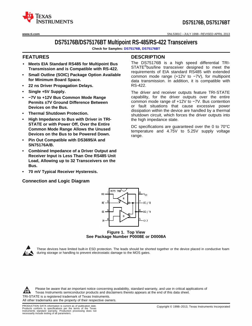
DS75176B/DS75176BT Multipoint RS-485/RS-422 TransceiversCheck for Samples: DS75176B, DS75176BT
1FEATURES DESCRIPTIONThe DS75176B is a high speed differential TRI-
23• Meets EIA Standard RS485 for Multipoint BusSTATE®bus/line transceiver designed to meet theTransmission and is Compatible with RS-422.requirements of EIA standard RS485 with extended
• Small Outline (SOIC) Package Option Available common mode range (+12V to −7V), for multipointfor Minimum Board Space. data transmission. In addition, it is compatible with
RS-422.• 22 ns Driver Propagation Delays.• Single +5V Supply. The driver and receiver outputs feature TRI-STATE
capability, for the driver outputs over the entire• −7V to +12V Bus Common Mode Rangecommon mode range of +12V to −7V. Bus contentionPermits ±7V Ground Difference Betweenor fault situations that cause excessive powerDevices on the Bus.dissipation within the device are handled by a thermal
• Thermal Shutdown Protection. shutdown circuit, which forces the driver outputs into• High Impedance to Bus with Driver in TRI- the high impedance state.
STATE or with Power Off, Over the EntireDC specifications are guaranteed over the 0 to 70°C
Common Mode Range Allows the Unused temperature and 4.75V to 5.25V supply voltageDevices on the Bus to be Powered Down. range.
• Pin Out Compatible with DS3695/A andSN75176A/B.
• Combined Impedance of a Driver Output andReceiver Input is Less Than One RS485 UnitLoad, Allowing up to 32 Transceivers on theBus.
• 70 mV Typical Receiver Hysteresis.
Connection and Logic Diagram
Figure 1. Top ViewSee Package Number P0008E or D0008A
These devices have limited built-in ESD protection. The leads should be shorted together or the device placed in conductive foamduring storage or handling to prevent electrostatic damage to the MOS gates.
1
Please be aware that an important notice concerning availability, standard warranty, and use in critical applications ofTexas Instruments semiconductor products and disclaimers thereto appears at the end of this data sheet.
2TRI-STATE is a registered trademark of Texas Instruments.3All other trademarks are the property of their respective owners.
PRODUCTION DATA information is current as of publication date. Copyright © 1998–2013, Texas Instruments IncorporatedProducts conform to specifications per the terms of the TexasInstruments standard warranty. Production processing does notnecessarily include testing of all parameters.

DS75176B, DS75176BT
SNLS381C –JULY 1998–REVISED APRIL 2013 www.ti.com
Absolute Maximum Ratings (1) (2)
Supply Voltage, VCC 7V
Control Input Voltages 7V
Driver Input Voltage 7V
Driver Output Voltages +15V/ −10V
Receiver Input Voltages (DS75176B) +15V/ −10V
Receiver Output Voltage 5.5V
Continuous Power Dissipation @ 25°C for SOIC Package 675 mW (3)
for PDIP Package 900 mW (4)
Storage Temperature Range −65°C to +150°C
Lead Temperature(Soldering, 4 seconds) 260°C
ESD Rating (HBM) 500V
(1) “Absolute Maximum Ratings” are those beyond which the safety of the device cannot be verified. They are not meant to imply that thedevice should be operated at these limits. The tables of “Electrical Characteristics” provide conditions for actual device operation.
(2) If Military/Aerospace specified devices are required, please contact the TI Sales Office/Distributors for availability and specifications.(3) Derate linearly @ 6.11 mW/°C to 400 mW at 70°C.(4) Derate linearly at 5.56 mW/°C to 650 mW at 70°C.
Recommended Operating ConditionsMin Max Units
Supply Voltage, VCC 4.75 5.25 V
Voltage at Any Bus Terminal −7 +12 V(Separate or Common Mode)
Operating Free Air Temperature TA
DS75176B 0 +70 °C
DS75176BT −40 +85 °C
Differential Input Voltage, VID (1) −12 +12 V
(1) Differential - Input/Output bus voltage is measured at the noninverting terminal A with respect to the inverting terminal B.
Electrical Characteristics (1) (2)
0°C ≤ TA≤ 70°C, 4.75V < VCC< 5.25V unless otherwise specified
Symbol Parameter Conditions Min Typ Max Units
VOD1 Differential Driver Output IO = 0 5 VVoltage (Unloaded)
VOD2 Differential Driver Output See (Figure 2) R = 50Ω; (RS-422) (3) 2 VVoltage (with Load) R = 27Ω; (RS-485) 1.5 V
ΔVOD Change in Magnitude of Driver
Differential Output Voltage For 0.2 V
Complementary Output States
VOC Driver Common Mode Output Voltage See (Figure 2) R = 27Ω3.0 V
Δ|VOC| Change in Magnitude of Driver
Common Mode Output Voltage0.2 V
For Complementary Output States
(1) All currents into device pins are positive; all currents out of device pins are negative. All voltages are referenced to device ground unlessotherwise specified.
(2) All typicals are given for VCC = 5V and TA = 25°C.(3) All worst case parameters for which this note is applied, must be increased by 10% for DS75176BT. The other parameters remain valid
for −40°C < TA < +85°C.
2 Submit Documentation Feedback Copyright © 1998–2013, Texas Instruments Incorporated
Product Folder Links: DS75176B DS75176BT

DS75176B, DS75176BT
www.ti.com SNLS381C –JULY 1998–REVISED APRIL 2013
Electrical Characteristics (1) (2) (continued)0°C ≤ TA≤ 70°C, 4.75V < VCC< 5.25V unless otherwise specified
Symbol Parameter Conditions Min Typ Max Units
VIH Input High Voltage 2 V
VIL Input Low Voltage 0.8DI, DE,VCL Input Clamp Voltage IIN = −18 mA −1.5RE , E
IIL Input Low Current VIL = 0.4V −200 μA
IIH Input High Current VIH = 2.4V 20 μA
IIN Input Current DO/RI, DO/RI VCC = 0V or 5.25V VIN = 12V +1.0 mA
DE = 0V VIN = −7V −0.8 mA
VTH Differential Input Threshold Voltage for −7V ≤ VCM ≤ + 12V −0. +0.2 VReceiver 2
ΔVTH Receiver Input Hysteresis VCM = 0V 70 mV
VOH Receiver Output High Voltage IOH = −400 μA 2.7 V
VOL Output Low Voltage RO IOL = 16 mA (3) 0.5 V
IOZR OFF-State (High Impedance) VCC = Max ±20 μA
Output Current at Receiver 0.4V ≤ VO ≤ 2.4V
RIN Receiver Input Resistance −7V ≤ VCM ≤ +12V 12 kΩICC Supply Current No Load (3) Driver Outputs Enabled 55 mA
Driver Outputs Disabled 35 mA
IOSD Driver Short-Circuit VO = −7V (3) −250 mA
Output Current VO = +12V (3) +250 mA
IOSR Receiver Short-Circuit VO = 0V −15 −85 mA
Output Current
Switching CharacteristicsVCC = 5.0V, TA = 25°C
Symbol Parameter Conditions Min Typ Max Units
tPLH Driver Input to Output RLDIFF = 60Ω 12 22 ns
tPHL Driver Input to Output CL1 = CL2 = 100 pF 17 22 ns
tr Driver Rise Time RLDIFF = 60Ω 18 ns
tf Driver Fall Time CL1 =CL2 = 100 pF 18 ns
(Figure 4 and Figure 6)
tZH Driver Enable to Output High CL = 100 pF (Figure 5 and Figure 7) S1 29 100 nsOpen
tZL Driver Enable to Output Low CL = 100 pF (Figure 5 and Figure 7) S2 31 60 nsOpen
tLZ Driver Disable Time from Low CL = 15 pF (Figure 5 and Figure 7) S2 13 30 nsOpen
tHZ Driver Disable Time from High CL = 15 pF (Figure 5 and Figure 7) S1 19 200 nsOpen
tPLH Receiver Input to Output CL = 15 pF (Figure 3 and Figure 8) 30 37 nsS1 and S2 ClosedtPHL Receiver Input to Output 32 37 ns
tZL Receiver Enable to Output Low CL = 15 pF (Figure 3 and Figure 9) S2 15 20 nsOpen
tZH Receiver Enable to Output High CL = 15 pF (Figure 3 and Figure 9) S1 11 20 nsOpen
tLZ Receiver Disable from Low CL = 15 pF (Figure 3 and Figure 9) S2 28 32 nsOpen
tHZ Receiver Disable from High CL = 15 pF (Figure 3 and Figure 9) S1 13 35 nsOpen
Copyright © 1998–2013, Texas Instruments Incorporated Submit Documentation Feedback 3
Product Folder Links: DS75176B DS75176BT

DS75176B, DS75176BT
SNLS381C –JULY 1998–REVISED APRIL 2013 www.ti.com
AC TEST CIRCUITS
Note: S1 and S2 of load circuit are closed except as otherwisementioned.
Figure 2. Figure 3.
Note: Unless otherwise specified the switches are closed.
Figure 4. Figure 5.
Switching Time Waveforms
Figure 6. Driver Propagation Delays and Transition Times
Figure 7. Driver Enable and Disable Times
4 Submit Documentation Feedback Copyright © 1998–2013, Texas Instruments Incorporated
Product Folder Links: DS75176B DS75176BT

DS75176B, DS75176BT
www.ti.com SNLS381C –JULY 1998–REVISED APRIL 2013
Note: Differential input voltage may may be realized by grounding RI and pulsing RI between +2.5V and −2.5V
Figure 8. Receiver Propagation Delays
Figure 9. Receiver Enable and Disable Times
Function Tables
Table 1. DS75176B Transmitting (1)
Inputs Line Condition Outputs
RE DE DI DO DO
X 1 1 No Fault 0 1
X 1 0 No Fault 1 0
X 0 X X Z Z
X 1 X Fault Z Z
(1) X — Don't care conditionZ — High impedance stateFault — Improper line conditons causing excessive power dissipationin the driver, such as shorts or bus contention situations**This is a fail safe condition
Copyright © 1998–2013, Texas Instruments Incorporated Submit Documentation Feedback 5
Product Folder Links: DS75176B DS75176BT

DS75176B, DS75176BT
SNLS381C –JULY 1998–REVISED APRIL 2013 www.ti.com
Table 2. DS75176B Receiving (1)
Inputs Outputs
RE DE RI-RI RO
0 0 ≥ +0.2V 1
0 0 ≤ −0.2V 0
0 0 Inputs Open** 1
1 0 X Z
(1) X — Don't care conditionZ — High impedance stateFault — Improper line conditons causing excessive power dissipationin the driver, such as shorts or bus contention situations**This is a fail safe condition
TYPICAL APPLICATION
6 Submit Documentation Feedback Copyright © 1998–2013, Texas Instruments Incorporated
Product Folder Links: DS75176B DS75176BT

DS75176B, DS75176BT
www.ti.com SNLS381C –JULY 1998–REVISED APRIL 2013
REVISION HISTORY
Changes from Revision B (April 2013) to Revision C Page
• Changed layout of National Data Sheet to TI format ............................................................................................................ 6
Copyright © 1998–2013, Texas Instruments Incorporated Submit Documentation Feedback 7
Product Folder Links: DS75176B DS75176BT

PACKAGE OPTION ADDENDUM
www.ti.com 12-Jul-2014
Addendum-Page 1
PACKAGING INFORMATION
Orderable Device Status(1)
Package Type PackageDrawing
Pins PackageQty
Eco Plan(2)
Lead/Ball Finish(6)
MSL Peak Temp(3)
Op Temp (°C) Device Marking(4/5)
Samples
DS75176BM NRND SOIC D 8 95 TBD Call TI Call TI 0 to 70 DS75176BM
DS75176BM/NOPB ACTIVE SOIC D 8 95 Green (RoHS& no Sb/Br)
CU SN Level-1-260C-UNLIM 0 to 70 DS75176BM
DS75176BMX NRND SOIC D 8 2500 TBD Call TI Call TI 0 to 70 DS75176BM
DS75176BMX/NOPB ACTIVE SOIC D 8 2500 Green (RoHS& no Sb/Br)
CU SN Level-1-260C-UNLIM 0 to 70 DS75176BM
DS75176BN LIFEBUY PDIP P 8 40 TBD Call TI Call TI 0 to 70 DS75176BN
DS75176BN/NOPB ACTIVE PDIP P 8 40 Green (RoHS& no Sb/Br)
CU SN Level-1-NA-UNLIM 0 to 70 DS75176BN
DS75176BTM NRND SOIC D 8 95 TBD Call TI Call TI -40 to 85 DS75176BTM
DS75176BTM/NOPB ACTIVE SOIC D 8 95 Green (RoHS& no Sb/Br)
CU SN Level-1-260C-UNLIM -40 to 85 DS75176BTM
DS75176BTMX NRND SOIC D 8 2500 TBD Call TI Call TI -40 to 85 DS75176BTM
DS75176BTMX/NOPB ACTIVE SOIC D 8 2500 Green (RoHS& no Sb/Br)
CU SN Level-1-260C-UNLIM -40 to 85 DS75176BTM
DS75176BTN LIFEBUY PDIP P 8 40 TBD Call TI Call TI -40 to 85 DS75176BTN
DS75176BTN/NOPB ACTIVE PDIP P 8 40 Green (RoHS& no Sb/Br)
CU SN Level-1-NA-UNLIM -40 to 85 DS75176BTN
(1) The marketing status values are defined as follows:ACTIVE: Product device recommended for new designs.LIFEBUY: TI has announced that the device will be discontinued, and a lifetime-buy period is in effect.NRND: Not recommended for new designs. Device is in production to support existing customers, but TI does not recommend using this part in a new design.PREVIEW: Device has been announced but is not in production. Samples may or may not be available.OBSOLETE: TI has discontinued the production of the device.
(2) Eco Plan - The planned eco-friendly classification: Pb-Free (RoHS), Pb-Free (RoHS Exempt), or Green (RoHS & no Sb/Br) - please check http://www.ti.com/productcontent for the latest availabilityinformation and additional product content details.TBD: The Pb-Free/Green conversion plan has not been defined.Pb-Free (RoHS): TI's terms "Lead-Free" or "Pb-Free" mean semiconductor products that are compatible with the current RoHS requirements for all 6 substances, including the requirement thatlead not exceed 0.1% by weight in homogeneous materials. Where designed to be soldered at high temperatures, TI Pb-Free products are suitable for use in specified lead-free processes.

PACKAGE OPTION ADDENDUM
www.ti.com 12-Jul-2014
Addendum-Page 2
Pb-Free (RoHS Exempt): This component has a RoHS exemption for either 1) lead-based flip-chip solder bumps used between the die and package, or 2) lead-based die adhesive used betweenthe die and leadframe. The component is otherwise considered Pb-Free (RoHS compatible) as defined above.Green (RoHS & no Sb/Br): TI defines "Green" to mean Pb-Free (RoHS compatible), and free of Bromine (Br) and Antimony (Sb) based flame retardants (Br or Sb do not exceed 0.1% by weightin homogeneous material)
(3) MSL, Peak Temp. - The Moisture Sensitivity Level rating according to the JEDEC industry standard classifications, and peak solder temperature.
(4) There may be additional marking, which relates to the logo, the lot trace code information, or the environmental category on the device.
(5) Multiple Device Markings will be inside parentheses. Only one Device Marking contained in parentheses and separated by a "~" will appear on a device. If a line is indented then it is a continuationof the previous line and the two combined represent the entire Device Marking for that device.
(6) Lead/Ball Finish - Orderable Devices may have multiple material finish options. Finish options are separated by a vertical ruled line. Lead/Ball Finish values may wrap to two lines if the finishvalue exceeds the maximum column width.
Important Information and Disclaimer:The information provided on this page represents TI's knowledge and belief as of the date that it is provided. TI bases its knowledge and belief on informationprovided by third parties, and makes no representation or warranty as to the accuracy of such information. Efforts are underway to better integrate information from third parties. TI has taken andcontinues to take reasonable steps to provide representative and accurate information but may not have conducted destructive testing or chemical analysis on incoming materials and chemicals.TI and TI suppliers consider certain information to be proprietary, and thus CAS numbers and other limited information may not be available for release.
In no event shall TI's liability arising out of such information exceed the total purchase price of the TI part(s) at issue in this document sold by TI to Customer on an annual basis.

TAPE AND REEL INFORMATION
*All dimensions are nominal
Device PackageType
PackageDrawing
Pins SPQ ReelDiameter
(mm)
ReelWidth
W1 (mm)
A0(mm)
B0(mm)
K0(mm)
P1(mm)
W(mm)
Pin1Quadrant
DS75176BMX SOIC D 8 2500 330.0 12.4 6.5 5.4 2.0 8.0 12.0 Q1
DS75176BMX/NOPB SOIC D 8 2500 330.0 12.4 6.5 5.4 2.0 8.0 12.0 Q1
DS75176BTMX SOIC D 8 2500 330.0 12.4 6.5 5.4 2.0 8.0 12.0 Q1
DS75176BTMX/NOPB SOIC D 8 2500 330.0 12.4 6.5 5.4 2.0 8.0 12.0 Q1
PACKAGE MATERIALS INFORMATION
www.ti.com 11-Oct-2013
Pack Materials-Page 1
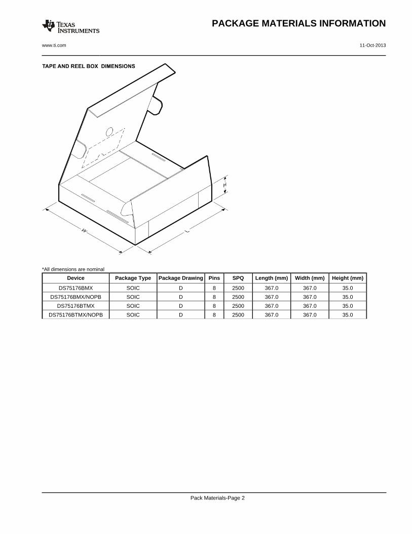
*All dimensions are nominal
Device Package Type Package Drawing Pins SPQ Length (mm) Width (mm) Height (mm)
DS75176BMX SOIC D 8 2500 367.0 367.0 35.0
DS75176BMX/NOPB SOIC D 8 2500 367.0 367.0 35.0
DS75176BTMX SOIC D 8 2500 367.0 367.0 35.0
DS75176BTMX/NOPB SOIC D 8 2500 367.0 367.0 35.0
PACKAGE MATERIALS INFORMATION
www.ti.com 11-Oct-2013
Pack Materials-Page 2


IMPORTANT NOTICETexas Instruments Incorporated and its subsidiaries (TI) reserve the right to make corrections, enhancements, improvements and otherchanges to its semiconductor products and services per JESD46, latest issue, and to discontinue any product or service per JESD48, latestissue. Buyers should obtain the latest relevant information before placing orders and should verify that such information is current andcomplete. All semiconductor products (also referred to herein as “components”) are sold subject to TI’s terms and conditions of salesupplied at the time of order acknowledgment.TI warrants performance of its components to the specifications applicable at the time of sale, in accordance with the warranty in TI’s termsand conditions of sale of semiconductor products. Testing and other quality control techniques are used to the extent TI deems necessaryto support this warranty. Except where mandated by applicable law, testing of all parameters of each component is not necessarilyperformed.TI assumes no liability for applications assistance or the design of Buyers’ products. Buyers are responsible for their products andapplications using TI components. To minimize the risks associated with Buyers’ products and applications, Buyers should provideadequate design and operating safeguards.TI does not warrant or represent that any license, either express or implied, is granted under any patent right, copyright, mask work right, orother intellectual property right relating to any combination, machine, or process in which TI components or services are used. Informationpublished by TI regarding third-party products or services does not constitute a license to use such products or services or a warranty orendorsement thereof. Use of such information may require a license from a third party under the patents or other intellectual property of thethird party, or a license from TI under the patents or other intellectual property of TI.Reproduction of significant portions of TI information in TI data books or data sheets is permissible only if reproduction is without alterationand is accompanied by all associated warranties, conditions, limitations, and notices. TI is not responsible or liable for such altereddocumentation. Information of third parties may be subject to additional restrictions.Resale of TI components or services with statements different from or beyond the parameters stated by TI for that component or servicevoids all express and any implied warranties for the associated TI component or service and is an unfair and deceptive business practice.TI is not responsible or liable for any such statements.Buyer acknowledges and agrees that it is solely responsible for compliance with all legal, regulatory and safety-related requirementsconcerning its products, and any use of TI components in its applications, notwithstanding any applications-related information or supportthat may be provided by TI. Buyer represents and agrees that it has all the necessary expertise to create and implement safeguards whichanticipate dangerous consequences of failures, monitor failures and their consequences, lessen the likelihood of failures that might causeharm and take appropriate remedial actions. Buyer will fully indemnify TI and its representatives against any damages arising out of the useof any TI components in safety-critical applications.In some cases, TI components may be promoted specifically to facilitate safety-related applications. With such components, TI’s goal is tohelp enable customers to design and create their own end-product solutions that meet applicable functional safety standards andrequirements. Nonetheless, such components are subject to these terms.No TI components are authorized for use in FDA Class III (or similar life-critical medical equipment) unless authorized officers of the partieshave executed a special agreement specifically governing such use.Only those TI components which TI has specifically designated as military grade or “enhanced plastic” are designed and intended for use inmilitary/aerospace applications or environments. Buyer acknowledges and agrees that any military or aerospace use of TI componentswhich have not been so designated is solely at the Buyer's risk, and that Buyer is solely responsible for compliance with all legal andregulatory requirements in connection with such use.TI has specifically designated certain components as meeting ISO/TS16949 requirements, mainly for automotive use. In any case of use ofnon-designated products, TI will not be responsible for any failure to meet ISO/TS16949.Products ApplicationsAudio www.ti.com/audio Automotive and Transportation www.ti.com/automotiveAmplifiers amplifier.ti.com Communications and Telecom www.ti.com/communicationsData Converters dataconverter.ti.com Computers and Peripherals www.ti.com/computersDLP® Products www.dlp.com Consumer Electronics www.ti.com/consumer-appsDSP dsp.ti.com Energy and Lighting www.ti.com/energyClocks and Timers www.ti.com/clocks Industrial www.ti.com/industrialInterface interface.ti.com Medical www.ti.com/medicalLogic logic.ti.com Security www.ti.com/securityPower Mgmt power.ti.com Space, Avionics and Defense www.ti.com/space-avionics-defenseMicrocontrollers microcontroller.ti.com Video and Imaging www.ti.com/videoRFID www.ti-rfid.comOMAP Applications Processors www.ti.com/omap TI E2E Community e2e.ti.comWireless Connectivity www.ti.com/wirelessconnectivity
Mailing Address: Texas Instruments, Post Office Box 655303, Dallas, Texas 75265Copyright © 2014, Texas Instruments Incorporated