Supports RS-232C, RS-422/485, TTL (UART, I2C, SPI) Multi ...
SP338ERS-232/RS-485/RS-422 TRANSCEIVER WITH INTERNAL TERMINATION
NOVEMBER 2011 REV. 1.0.0
GENERAL DESCRIPTIONThe SP338 is an advanced multiprotocol transceiver supporting RS-232, RS-485, and RS-422 serial standards in a 40 pin QFN package. Integrated cable termination and four configuration modes allow all three protocols to be used interchangeably over a single cable or connector with no additional switching components. Full operation requires only four external charge pump capacitors.
The RS-485/422 modes feature up to two drivers and four receivers (2TX/4RX) in half, full, and mixed duplex configurations. The RS-232 mode (3TX/5RX) provides full support of all eight signals commonly used with the DB9 RS-232 connector. A dedicated diagnostic loopback mode is also provided.
The high speed drivers operate up to 20Mbps in RS-485/422 modes, and up to 1Mbps in RS-232 mode. All drivers can be slew limited to 250kbps in any mode to minimize electromagnetic interference (EMI).
All transmitter outputs and receiver inputs feature robust electrostatic discharge (ESD) protection to ±15kV Human Body Model (HBM) and ±8kV IEC-61000-4-2 Contact. Each receiver output has full fail-safe protection to avoid system lockup, oscillation, or indeterminate states by defaulting to logic-high output level when the inputs are open, shorted, or terminated but undriven. No external biasing resistors are required.
The RS-232 receiver inputs include a 5kΩ pull-down to ground. The RS-485/422 receiver inputs are high impedance (>96kΩ when termination is disabled), allowing up to 256 devices on a single communication bus (1/8th unit load).
The SP338 operates from a single power supply, either 3.3V or 5V, with low idle current. The shutdown mode consumes less than 10µA for low power standby operation.
FEATURES
• Pin selectable Cable Termination
• No external resistors required for RS-485/422 termination and biasing
• 3.3V or 5V Single Supply Operation
• Robust ESD Protection on bus pins
±15kV Human Body Model (HBM) ±8kV IEC 61000-4-2 (Contact)
• Max Data Rate of 20Mbps in RS-485/422 Modes and up to 1Mbps in RS-232 Modes
• Pin selectable 250kbps Slew Limiting
• 3 Drivers, 5 Receivers RS-232/V.28
• 2 Drivers, 4 Receivers RS-485/422
Full, Half, and Mixed Duplex Configurations 1/8th Unit Load, up to 256 receivers on bus
• RS-485/422 Enhanced Failsafe for open, shorted, or terminated but idle inputs
• Space saving 6mm x 6mm QFN-40 Package
• Pin compatible with SP339E
TYPICAL APPLICATIONS
• Dual Protocol Serial Ports (RS-232 or RS-485/422)
• Industrial Computers
• Industrial and Process Control Equipment
• Point-Of-Sale Equipment
• Networking Equipment
• HVAC Controls Equipment
• Building Security and Automation Equipment
Exar Corporation 48720 Kato Road, Fremont CA, 94538 • (510) 668-7000 • FAX (510) 668-7017 • www.exar.com
ORDERING INFORMATION
PART NUMBER PACKAGE OPERATING TEMPERATURE RANGE DEVICE STATUS
SP338EER1-L 40-pin QFN -40°C to +85°C Active
SP338EER1-L/TR 40-pin QFN -40°C to +85°C Active
SP338ECR1-L 40-pin QFN 0°C to +70°C Active
SP338ECR1-L/TR 40-pin QFN 0°C to +70°C Active
SP338E RS-232/RS-485/RS-422 TRANSCEIVER WITH INTERNAL TERMINATION REV. 1.0.0
ABSOLUTE MAXIMUM RATINGSThese are stress ratings only and functional operation of the device at these ratings or any other above those indicated in the operation sections to the specifications below is not implied. Exposure to absolute maximum rating conditions for extended periods of time may affect reliability and cause permanent damage to the device.
Supply Voltage VCC -0.3V to +6.0V
Receiver Input Voltage (from Ground) ±18V
Driver Output Voltage (from Ground) ±18V
Short Circuit Duration, TX out to Ground Continuous
Voltage at TTL Input Pins -0.3V to (VCC + 0.5V)
Storage Temperature Range -65°C to +150°C
Lead Temperature (soldering, 10s) +300°C
Power Dissipation 40-pin QFN(derate 17mW/°C above +70°C)
500mW
CAUTION:
ESD (ElectroStatic Discharge) sensitive device. Permanent damage may occur on unconnected devices subject to high energy electrostatic fields. Unused devices must be stored in conductive foam or shunts. Personnel should be properly grounded prior to handling this device. The protective foam should be discharged to the destination socket before devices are removed.
ESD PROTECTION
MIN. TYP. MAX. UNITS
R1-R9 Tx Output & Rx Input Pins±15 kV Human Body Model (HBM)
±8 kV IEC 61000-4-2 (Contact)
All Other Pins ±2 kV Human Body Model (HBM)
2

SP338EREV. 1.0.0 RS-232/RS-485/RS-422 TRANSCEIVER WITH INTERNAL TERMINATION
PIN DESCRIPTIONS BY MODE (MODE2, MODE1, MODE0)
Pin Name000,
Figure 1001,
Figure 2010,
Figure 3011,
Figure 4100,
Figure 5101,
Figure 6110,
Figure 7111,
Figure 8
1 L1 R1 Output 1 1 1 1 1 1
2 L2 R2 Output R1 Output R1 Output R1 Output R1 Output R1 Output R1 Output
3 L3 T1 Input T1 Input T1 Input T1 Input T1 Input T1 Input T1 Input
4 L4 T2 Input
5 L6 R3 Output 1 1 1 1 1 R2 Output
6 L7 T3 Input T2 Input T2 Input
7 L8 R4 Output 1 1 R2 Output 1 1 R3 Output
8 L9 R5 Output 1 1 1 1 1 R4 Output
9 VCC VCC
10 GND Ground
11 SLEW SLEW = VCC enables 250kbps slew limiting
12 DIR1 T1 Enable, R1 Disable T1 Enable T1 Enable T1 Enable T1 Enable,
R1 DisableT1 Enable, R1 Disable
13 DIR2 T2 Enable T2 Enable, R2 Disable
14 MODE0 0 1 0 1 0 1 0 1
15 MODE1 0 0 1 1 0 0 1 1
16 MODE2 0 0 0 0 1 1 1 1
17 TERM Enables RS-485/422 receiver termination
18 INVDIR Inverts DIR1 and DIR2, where applicable
19 ENABLE ENABLE = VCC for operation, ENABLE = 0V for shutdown
20 VCC VCC
3

SP338E RS-232/RS-485/RS-422 TRANSCEIVER WITH INTERNAL TERMINATION REV. 1.0.0
PIN DESCRIPTIONS BY MODE (MODE2, MODE1, MODE0)
Pin Name000,
Figure 1001,
Figure 2010,
Figure 3011,
Figure 4100,
Figure 5101,
Figure 6110,
Figure 7111,
Figure 8
21 R9 R5 Input R2 Input B R1 Input B R4 Input B
22 R8 R4 Input R2 Input A R4 Input A
23 GND Ground
24 R7 T3 Output T2 Out A R1 Input AR3 Input AT2 Out A
25 R6 R3 Input T2 Out BR3 Input BT2 Out B
26 GND Ground
27 R4 T2 Output R1 Input B R1 Input B T1 Out AR1 Input AT1 Out A
R2 Input B
28 R3 T1 Output R2 Input A R1 Input A R2 Input A
29 GND Ground
30 R2 R2 InputR1 Input AT1 Out A
T1 Out A T1 Out AR1 Input AT1 Out A
31 R1 R1 InputR1 Input BT1 Out B
T1 Out B T1 Out B T1 Out BR1 Input BT1 Out B
R1 Input BT1 Out B
32 VCC VCC
33 VSS VSS - Charge pump negative supply, 0.1uF from ground
34 C2- C2+ - Charge pump cap 2 negative lead
35 C1- C1- - Charge pump cap 1 negative lead
36 GND Ground
37 C1+ C1+ - Charge pump cap 1 positive lead, 0.1uF
38 VCC VCC
39 C2+ C2+ - Charge pump cap 2 positive lead, 0.1uF
40 VDD VDD - Charge pump positive supply, 0.1uF to ground
4

SP338EREV. 1.0.0 RS-232/RS-485/RS-422 TRANSCEIVER WITH INTERNAL TERMINATION
ELECTRICAL CHARACTERISTICSUNLESS OTHERWISE NOTED: VCC = +3.3V ±5% or +5.0V ±5%, C1-C4 = 0.1µF; TA = TMIN to TMAX. Typical values are at VCC = 3.3V, TA = +25°C.
SYMBOL PARAMETERS MIN. TYP. MAX. UNITS CONDITIONS
DC CHARACTERISTICS
ICC Supply Current (RS-232) 2 10 mA No load, idle inputs
ICC Supply Current (RS-485) 4 10 mA No load, idle inputs
ICC Vcc Shutdown Current 1 10 µA ENABLE = 0V
TRANSMITTER and LOGIC INPUT PINS: Pins 3, 4, 6, 11-19
VIH Logic Input Voltage High 2.0 V VCC = 3.3V
VIH Logic Input Voltage High 2.4 V VCC = 5.0V
VIL Logic Input Voltage Low 0.8 V
IIL Logic Input Leakage Current Low 1 µA Input Low (VIN = 0V)
IIH Logic Input Leakage Current High 1 µAInput High (VIN = VCC), pins 3, 4 and 6
IPD Logic Input Pull-down Current 50 µAInput High (VIN = VCC), pins 11-19
VHYS Logic Input Hysteresis 200 mV
RECEIVER OUTPUTS: Pins 1, 2, 5, 7, 8
VOH Receiver Output Voltage High VCC-0.6 V IOUT = -1.5mA
VOL Receiver Output Voltage Low 0.4 V IOUT = 2.5mA
IOSS Receiver Output ShortCircuit Current ±20 ±60 mA 0 ≤ VO ≤ VCC
IOZ Receiver Output Leakage Current ±0.1 ±1 µA0 ≤ VO ≤ VCC,
Receivers disabled
5

SP338E RS-232/RS-485/RS-422 TRANSCEIVER WITH INTERNAL TERMINATION REV. 1.0.0
UNLESS OTHERWISE NOTED: VCC = +3.3V ±5% or +5.0V ±5%, C1-C4 = 0.1µF; TA = TMIN to TMAX. Typical values are at VCC = 3.3V, TA = +25°C.
SYMBOL PARAMETERS MIN. TYP. MAX. UNITS CONDITIONS
SINGLE-ENDED RECEIVER INPUTS (RS-232)
VIN Input Voltage Range -15 +15 V
VIL Input Threshold Low0.6 1.2 V VCC = 3.3V
0.8 1.5 V VCC = 5.0V
VIH Input Threshold High1.5 2.0 V VCC = 3.3V
1.8 2.4 V VCC = 5.0V
VHYS Input Hysteresis 0.3 V
RIN Input Resistance 3 5 7 kΩ -15V ≤ VIN ≤ +15V
SINGLE-ENDED DRIVER OUTPUTS (RS-232)
VO Output Voltage Swing±5.0 ±5.5 V Output loaded with 3kΩ to Gnd
±7.0 V No load output
ISC Short Circuit Current ±60 mA VO = 0V
ROFF Power Off Impedance 300 10M Ω VCC = 0V, VO = ±2V
ELECTRICAL CHARACTERISTICS (Continued)
6
SP338EREV. 1.0.0 RS-232/RS-485/RS-422 TRANSCEIVER WITH INTERNAL TERMINATION
ELECTRICAL CHARACTERISTICS (Continued)UNLESS OTHERWISE NOTED: VCC = +3.3V ±5% or +5.0V ±5%, C1-C4 = 0.1µF; TA = TMIN to TMAX. Typical values are at VCC = 3.3V, TA = +25°C.
SYMBOL PARAMETERS MIN. TYP. MAX. UNITS CONDITIONS
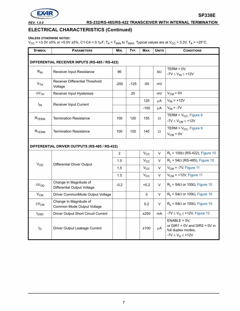
DIFFERENTIAL RECEIVER INPUTS (RS-485 / RS-422)
RIN Receiver Input Resistance 96 kΩTERM = 0V,-7V ≤ VIN ≤ +12V
VTHReceiver Differential Threshold Voltage
-200 -125 -50 mV
∆VTH Receiver Input Hysteresis 25 mV VCM = 0V
IIN Receiver Input Current125 µA VIN = +12V
-100 µA VIN = -7V
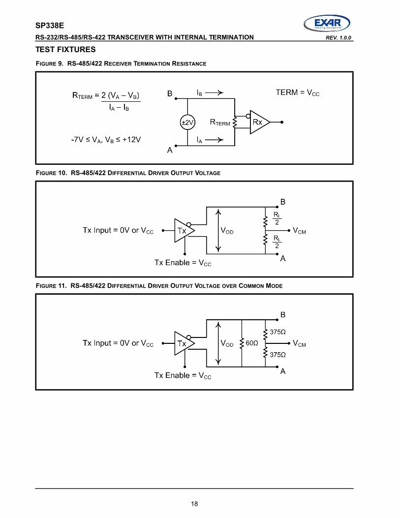
RTERM Termination Resistance 100 120 155 ΩTERM = VCC, Figure 9-7V ≤ VCM ≤ +12V
RTERM Termination Resistance 100 120 140 ΩTERM = VCC, Figure 9VCM = 0V
DIFFERENTIAL DRIVER OUTPUTS (RS-485 / RS-422)
VOD Differential Driver Output
2 VCC V RL = 100Ω (RS-422), Figure 10
1.5 VCC V RL = 54Ω (RS-485), Figure 10
1.5 VCC V VCM = -7V, Figure 11
1.5 VCC V VCM = +12V, Figure 11
∆VODChange In Magnitude ofDifferential Output Voltage
-0.2 +0.2 V RL = 54Ω or 100Ω, Figure 10
VCM Driver CommonMode Output Voltage 3 V RL = 54Ω or 100Ω, Figure 10
∆VCMChange In Magnitude ofCommon Mode Output Voltage
0.2 V RL = 54Ω or 100Ω, Figure 10
IOSD Driver Output Short Circuit Current ±250 mA -7V ≤ VO ≤ +12V, Figure 12
IO Driver Output Leakage Current ±100 µA
ENABLE = 0V,or DIR1 = 0V and DIR2 = 0V in full duplex modes,-7V ≤ VO ≤ +12V
7

SP338E RS-232/RS-485/RS-422 TRANSCEIVER WITH INTERNAL TERMINATION REV. 1.0.0
TIMING CHARACTERISTICSUNLESS OTHERWISE NOTED: VCC = +3.3V ±5% or +5.0V ±5%, C1-C4 = 0.1µF; TA = TMIN to TMAX. Typical values are at VCC = 3.3V, TA = +25°C.
SYMBOL PARAMETERS MIN. TYP. MAX. UNITS CONDITIONS
ALL MODES
tENABLE Enable from Shutdown 1000 ns
tSHUTDOWN Enable to Shutdown 1000 ns
RS-232, DATA RATE = 250kbps (SLEW = Vcc), ONE TRANSMITTER SWITCHING
Maximum Data Rate 250 kbps RL = 3kΩ, CL = 1000pF
tRHL, tRLH Receiver Propagation Delay 100 nsCL = 150pF, Figure 13
tRHL-tRLH Receiver Propagation Delay Skew 100 ns
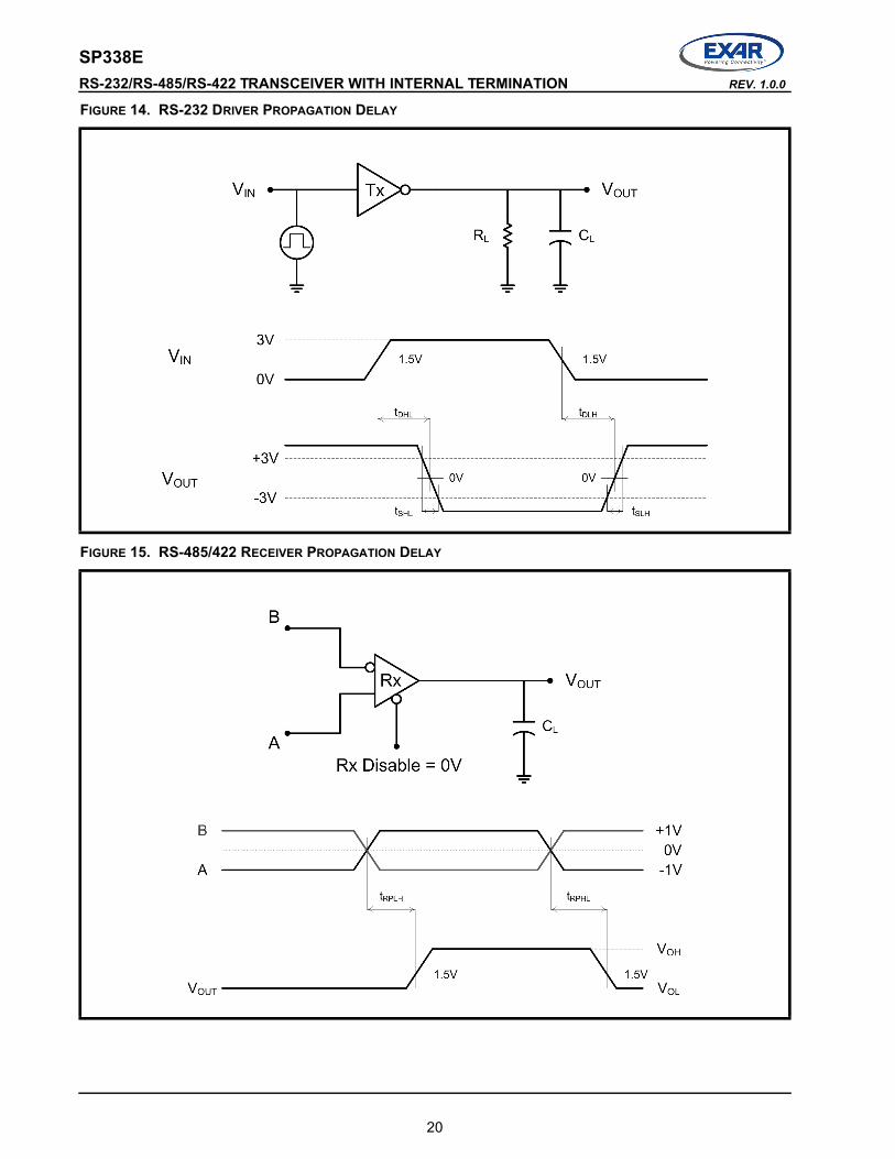
tDHL, tDLH Driver Propagation Delay 1400 ns RL = 3kΩ, CL = 2500pF,Figure 14tDHL-tDLH Driver Propagation Delay Skew 600 ns
tSHL, tSLHTransition Region Slew Rate from +3.0V to -3.0V or -3.0V to +3.0V 4 30 V/µs
VCC = 3.3V, RL = 3kΩ to 7kΩ,
CL = 150pF to 2500pF,Figure 14
tSHL, tSLHTransition Region Slew Rate from +3.0V to -3.0V or -3.0V to +3.0V 6 30 V/µs
VCC = 3.3V, RL = 3kΩ to 7kΩ,
CL = 150pF to 2500pF,TA = 25°C, Figure 14
RS-232, DATA RATE = 1Mbps (SLEW = 0V), ONE TRANSMITTER SWITCHING
Maximum Data Rate 1 Mbps RL = 3kΩ, CL = 250pF
tRHL, tRLH Receiver Propagation Delay 100 nsCL = 150pF, Figure 13
tRHL-tRLH Receiver Propagation Delay Skew 100 ns
tDHL, tDLH Driver Propagation Delay 300 ns RL = 3kΩ, CL = 1000pF,Figure 14tDHL-tDLH Driver Propagation Delay Skew 150 ns
tSHL, tSLHTransition Region Slew Rate from +3.0V to -3.0V or -3.0V to +3.0V 15 150 V/µs
VCC = 3.3V, RL = 3kΩ to 7kΩ,
CL = 150pF to 1000pF,Figure 14
tSHL, tSLHTransition Region Slew Rate from +3.0V to -3.0V or -3.0V to +3.0V 24 150 V/µs
VCC = 3.3V, RL = 3kΩ to 7kΩ,
CL = 150pF to 1000pF,TA = 25°C, Figure 14
8
SP338EREV. 1.0.0 RS-232/RS-485/RS-422 TRANSCEIVER WITH INTERNAL TERMINATION
TIMING CHARACTERISTICS (Continued)UNLESS OTHERWISE NOTED: VCC = +3.3V ±5% or +5.0V ±5%, C1-C4 = 0.1µF; TA = TMIN to TMAX. Typical values are at VCC = 3.3V, TA = +25°C.
SYMBOL PARAMETERS MIN. TYP. MAX. UNITS CONDITIONS
RS-485/RS-422, DATA RATE = 250kbps (SLEW = Vcc), ONE TRANSMITTER SWITCHING
Maximum Data Rate 250 kbps RL = 54Ω, CL = 50pF
tRPHL, tRPLH Receiver Propagation Delay 50 150 nsCL = 15pF, Figure 15
tRPHL-tRPLH Receiver Propagation Delay Skew 20 ns
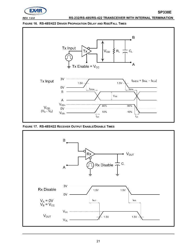
tDPHL, tDPLH Driver Propagation Delay 500 1000 nsRL = 54Ω, CL = 50pF,Figure 16
tDPHL-tDPLH Driver Propagation Delay Skew 100 ns
tDR, tDF Driver Rise and Fall Time 300 650 1200 ns
tRZH, tRZL Receiver Output Enable Time 200 nsCL = 15pF, Figure 17
tRHZ, tRLZ Receiver Output Disable Time 200 ns
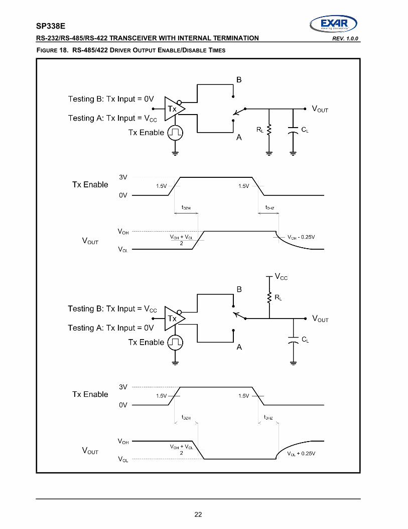
tDZH, tDZL Driver Output Enable Time 1000 ns RL = 500Ω, CL = 50pF,Figure 18tDHZ, tDLZ Driver Output Disable Time 200 ns
RS-485/RS-422, DATA RATE = 20Mbps (SLEW = 0V), ONE TRANSMITTER SWITCHING
Maximum Data Rate 20 Mbps RL = 54Ω, CL = 50pF
tRPHL, tRPLH Receiver Propagation Delay 50 150 nsCL = 15pF, Figure 15
tRPHL-tRPLH Receiver Propagation Delay Skew 10 ns
tDPHL, tDPLH Driver Propagation Delay 30 100 nsRL = 54Ω, CL = 50pF,Figure 16
tDPHL-tDPLH Driver Propagation Delay Skew 10 ns
tDR, tDF Driver Rise and Fall Time 10 20 ns
tRZH, tRZL Receiver Output Enable Time 200 nsCL = 15pF, Figure 17
tRHZ, tRLZ Receiver Output Disable Time 200 ns
tDZH, tDZL Driver Output Enable Time 200 ns RL = 500Ω, CL = 50pF,Figure 18tDHZ, tDLZ Driver Output Disable Time 200 ns
9

SP338E RS-232/RS-485/RS-422 TRANSCEIVER WITH INTERNAL TERMINATION REV. 1.0.0
BLOCK DIAGRAM BY MODE (MODE2, MODE1, MODE0)
FIGURE 1. MODE 000 - LOOPBACK
10
SP338EREV. 1.0.0 RS-232/RS-485/RS-422 TRANSCEIVER WITH INTERNAL TERMINATION
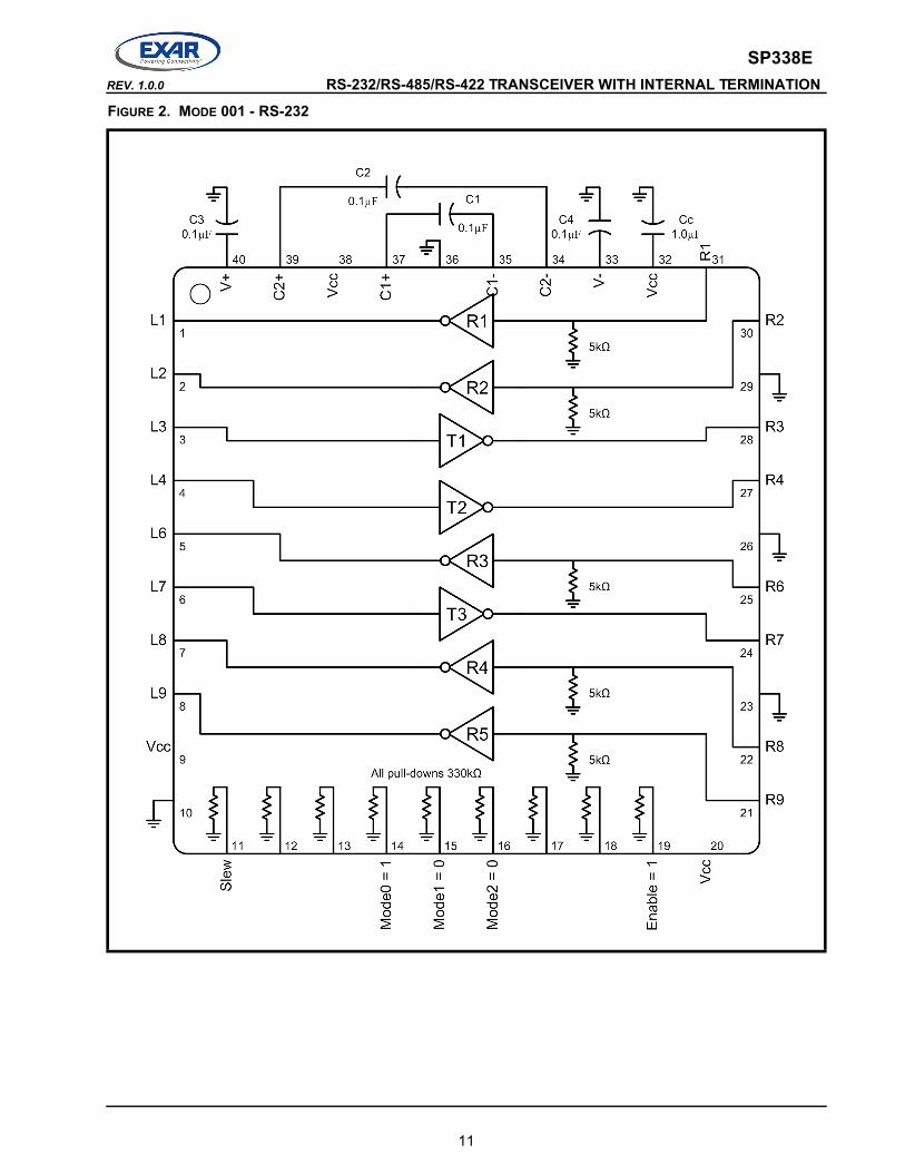
FIGURE 2. MODE 001 - RS-232
11
SP338E RS-232/RS-485/RS-422 TRANSCEIVER WITH INTERNAL TERMINATION REV. 1.0.0
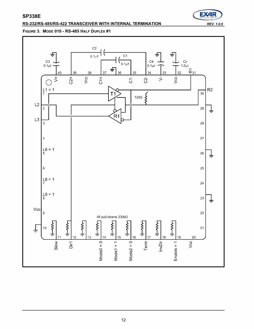
FIGURE 3. MODE 010 - RS-485 HALF DUPLEX #1
12

SP338EREV. 1.0.0 RS-232/RS-485/RS-422 TRANSCEIVER WITH INTERNAL TERMINATION
FIGURE 4. MODE 011 - RS-485/422 FULL DUPLEX #1
13
SP338E RS-232/RS-485/RS-422 TRANSCEIVER WITH INTERNAL TERMINATION REV. 1.0.0
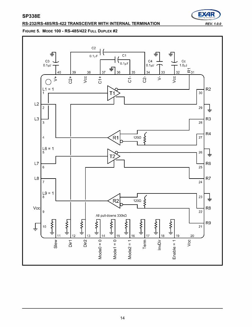
FIGURE 5. MODE 100 - RS-485/422 FULL DUPLEX #2
14
SP338EREV. 1.0.0 RS-232/RS-485/RS-422 TRANSCEIVER WITH INTERNAL TERMINATION
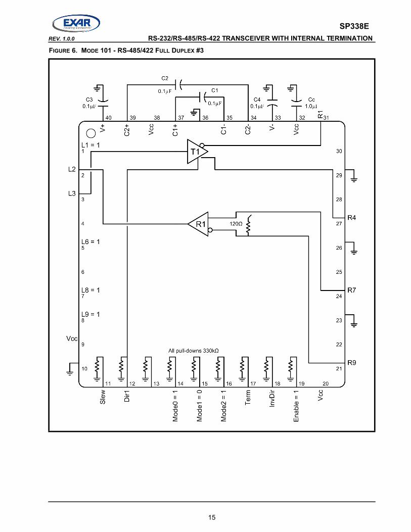
FIGURE 6. MODE 101 - RS-485/422 FULL DUPLEX #3
15
SP338E RS-232/RS-485/RS-422 TRANSCEIVER WITH INTERNAL TERMINATION REV. 1.0.0
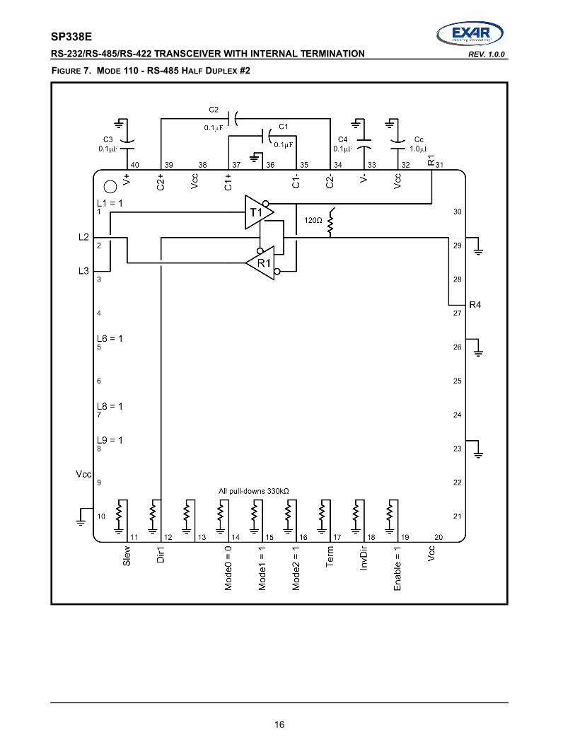
FIGURE 7. MODE 110 - RS-485 HALF DUPLEX #2
16
SP338EREV. 1.0.0 RS-232/RS-485/RS-422 TRANSCEIVER WITH INTERNAL TERMINATION
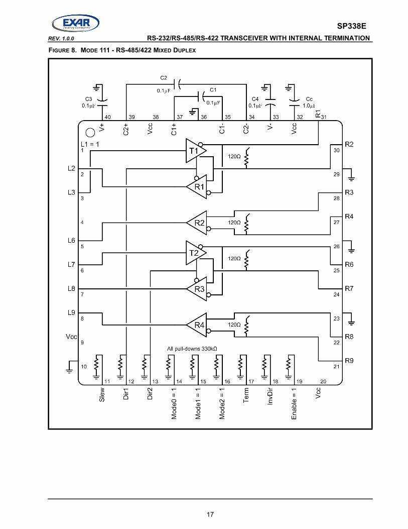
FIGURE 8. MODE 111 - RS-485/422 MIXED DUPLEX
17
SP338E RS-232/RS-485/RS-422 TRANSCEIVER WITH INTERNAL TERMINATION REV. 1.0.0
FIGURE 9. RS-485/422 RECEIVER TERMINATION RESISTANCE
FIGURE 10. RS-485/422 DIFFERENTIAL DRIVER OUTPUT VOLTAGE
FIGURE 11. RS-485/422 DIFFERENTIAL DRIVER OUTPUT VOLTAGE OVER COMMON MODE
TEST FIXTURES
18
SP338EREV. 1.0.0 RS-232/RS-485/RS-422 TRANSCEIVER WITH INTERNAL TERMINATION
FIGURE 12. RS-485/422 DRIVER OUTPUT SHORT CIRCUIT CURRENT
FIGURE 13. RS-232 RECEIVER PROPAGATION DELAY
19
SP338E RS-232/RS-485/RS-422 TRANSCEIVER WITH INTERNAL TERMINATION REV. 1.0.0
FIGURE 14. RS-232 DRIVER PROPAGATION DELAY
FIGURE 15. RS-485/422 RECEIVER PROPAGATION DELAY
20
SP338EREV. 1.0.0 RS-232/RS-485/RS-422 TRANSCEIVER WITH INTERNAL TERMINATION
FIGURE 16. RS-485/422 DRIVER PROPAGATION DELAY AND RISE/FALL TIMES
FIGURE 17. RS-485/422 RECEIVER OUTPUT ENABLE/DISABLE TIMES
21
SP338E RS-232/RS-485/RS-422 TRANSCEIVER WITH INTERNAL TERMINATION REV. 1.0.0
FIGURE 18. RS-485/422 DRIVER OUTPUT ENABLE/DISABLE TIMES
22
SP338EREV. 1.0.0 RS-232/RS-485/RS-422 TRANSCEIVER WITH INTERNAL TERMINATION
PRODUCT SUMMARY The SP338 is an advanced multiprotocol transceiver supporting RS-232, RS-485, and RS-422 serial standards in a 40 pin QFN package. Integrated cable termination and four configuration modes allow all three protocols to be used interchangeably over a single cable or connector with no additional switching components. The RS-485/422 modes feature up to two drivers and four receivers (2TX/4RX) in half, full, and mixed duplex configurations. The RS-232 mode (3TX/5RX) provides full support of all eight signals commonly used with the DB9 RS-232 connector. A dedicated mode is also available for diagnostic loopback testing.
INTERNALLY SWITCHED CABLE TERMINATION
Enabling and disabling the RS-485/422 termination resistor is one of the largest challenges system designers face when sharing a single connector or pair of lines between multiple serial protocols. A termination resistor may be necessary for accurate RS-485/422 communication, but must be removed when the lines are used for RS-232. SP338 provides an elegant solution to this problem by integrating the termination resistor and switching control, and allowing it to be switched in and out of the circuit with a single pin. No external switching components are required.
ENHANCED FAILSAFE
Ordinary RS-485 differential receivers will be in an indeterminate state whenever the data bus is not being actively driven. The enhanced failsafe feature of the SP338 guarantees a logic-high receiver output when the receiver inputs are open, shorted, or terminated but idle/undriven. The enhanced failsafe interprets 0V differential as a logic high with a minimum 50mV noise margin, while maintaining compliance with the EIA/TIA-485 standard of ±200mV. No external biasing resistors are required, further easing the usage of multiple protocols over a single connector.
±15kV ESD PROTECTION
ESD protection structures are incorporated on all pins to protect against electrostatic discharges encountered during handling and assembly. The bus pins (driver outputs and receiver inputs) have extra protection structures, which have been tested up to ±15kV without damage. These structures withstand high ESD in all states: normal operation, shutdown and powered down.
ESD protection is be tested in various ways. Exar uses the following methods to qualify the protection structures designed into SP338:
±15kV using the Human Body Model (HBM)
±-8kV using IEC 61000-4-2 Contact Discharge
The IEC 61000-4-2 standard is more rigorous than HBM, resulting in lower voltage levels compared with HBM for the same level of ESD protection. Because IEC 61000-4-2 specifies a lower series resistance, the peak current is higher than HBM. The SP338 has passed both HBM and IEC 61000-4-2 testing without damage.
DIAGNOSTIC LOOPBACK MODE
The SP338 includes a diagnostic digital loop back mode for system testing as shown in Figure 1. The loopback mode connects the TTL driver inputs to the TTL receiver outputs, bypassing the analog driver and receiver circuitry. The analog/bus pins are internally disconnected in this mode.
23
SP338E RS-232/RS-485/RS-422 TRANSCEIVER WITH INTERNAL TERMINATION REV. 1.0.0
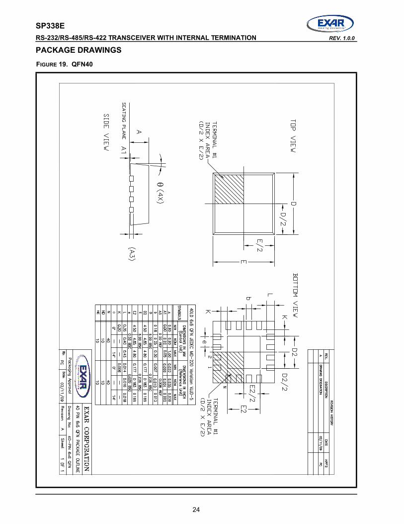
FIGURE 19. QFN40
PACKAGE DRAWINGS
24
SP338E
RS-232/RS-485/RS-422 TRANSCEIVER WITH INTERNAL TERMINATION REV. 1.0.0
REVISION HISTORY
DATE REVISION DESCRIPTION
November 2011 1.0.0 Production Release
25
NOTICE
EXAR Corporation reserves the right to make changes to the products contained in this publication in order to improve design, performance or reliability. EXAR Corporation assumes no responsibility for the use of any circuits described herein, conveys no license under any patent or other right, and makes no representation that the circuits are free of patent infringement. Charts and schedules contained here in are only for illustration purposes and may vary depending upon a user’s specific application. While the information in this publication has been carefully checked; no responsibility, however, is assumed for inaccuracies.
EXAR Corporation does not recommend the use of any of its products in life support applications where the failure or malfunction of the product can reasonably be expected to cause failure of the life support system or to significantly affect its safety or effectiveness. Products are not authorized for use in such applications unless EXAR Corporation receives, in writing, assurances to its satisfaction that: (a) the risk of injury or damage has been minimized; (b) the user assumes all such risks; (c) potential liability of EXAR Corporation is adequately protected under the circumstances.
Copyright 2011 EXAR Corporation
Datasheet November 2011.
For technical support please email Exar’s Serial Technical Support group at: [email protected].
Reproduction, in part or whole, without the prior written consent of EXAR Corporation is prohibited.