DS10BR150 1.0 Gbps LVDS Buffer / Repeater datasheet (Rev. D)
17
ASIC / FPGA CML LVDS LVPECL ASIC / FPGA LVDS BR150 DS10BR150 www.ti.com SNLS252D – APRIL 2007 – REVISED APRIL 2013 DS10BR150 1.0 Gbps LVDS Buffer / Repeater Check for Samples: DS10BR150 1FEATURES DESCRIPTION The DS10BR150 is a single channel 1.0 Gbps LVDS 2• DC - 1.0 Gbps Low Jitter, High Noise buffer optimized for high-speed signal transmission Immunity, Low Power Operation over lossy FR-4 printed circuit board backplanes and • On-chip 100Ω Input and Output Termination balanced cables. Fully differential signal paths ensure Minimizes Insertion and Return Losses, exceptional signal integrity and noise immunity. Reduces Component Count and Minimizes Wide input common mode range allows the receiver Board Space to accept signals with LVDS, CML and LVPECL • 7 kV ESD on LVDS I/O Pins Protects Adjoining levels; the output levels are LVDS. A very small Components package footprint requires a minimal space on the board while the flow-through pinout allows easy board • Small 3 mm x 3 mm 8-WSON Space Saving layout. The differential inputs and outputs are Package internally terminated with a 100Ω resistor to lower device input and output return losses, reduce APPLICATIONS component count and further minimize board space. • Clock and Data Buffering • OC-12 / STM-4 • FireWire 800 Typical Application 1 Please be aware that an important notice concerning availability, standard warranty, and use in critical applications of Texas Instruments semiconductor products and disclaimers thereto appears at the end of this data sheet. 2All trademarks are the property of their respective owners. PRODUCTION DATA information is current as of publication date. Copyright © 2007–2013, Texas Instruments Incorporated Products conform to specifications per the terms of the Texas Instruments standard warranty. Production processing does not necessarily include testing of all parameters.
Transcript of DS10BR150 1.0 Gbps LVDS Buffer / Repeater datasheet (Rev. D)

ASIC / FPGA
CML
LVDS
LVPECL
ASIC / FPGALVDSBR150
DS10BR150
www.ti.com SNLS252D –APRIL 2007–REVISED APRIL 2013
DS10BR150 1.0 Gbps LVDS Buffer / RepeaterCheck for Samples: DS10BR150
1FEATURES DESCRIPTIONThe DS10BR150 is a single channel 1.0 Gbps LVDS
2• DC - 1.0 Gbps Low Jitter, High Noisebuffer optimized for high-speed signal transmissionImmunity, Low Power Operationover lossy FR-4 printed circuit board backplanes and
• On-chip 100Ω Input and Output Termination balanced cables. Fully differential signal paths ensureMinimizes Insertion and Return Losses, exceptional signal integrity and noise immunity.Reduces Component Count and Minimizes
Wide input common mode range allows the receiverBoard Spaceto accept signals with LVDS, CML and LVPECL
• 7 kV ESD on LVDS I/O Pins Protects Adjoining levels; the output levels are LVDS. A very smallComponents package footprint requires a minimal space on the
board while the flow-through pinout allows easy board• Small 3 mm x 3 mm 8-WSON Space Savinglayout. The differential inputs and outputs arePackageinternally terminated with a 100Ω resistor to lowerdevice input and output return losses, reduceAPPLICATIONScomponent count and further minimize board space.
• Clock and Data Buffering• OC-12 / STM-4• FireWire 800
Typical Application
1
Please be aware that an important notice concerning availability, standard warranty, and use in critical applications ofTexas Instruments semiconductor products and disclaimers thereto appears at the end of this data sheet.
2All trademarks are the property of their respective owners.
PRODUCTION DATA information is current as of publication date. Copyright © 2007–2013, Texas Instruments IncorporatedProducts conform to specifications per the terms of the TexasInstruments standard warranty. Production processing does notnecessarily include testing of all parameters.

NC
IN+
IN-
NC
VCC
OUT+
OUT-
NC
1
2
3
4
8
6
5
7
GND
DAP
OUT+
OUT-
IN+
IN-
DS10BR150
SNLS252D –APRIL 2007–REVISED APRIL 2013 www.ti.com
Block Diagram
Pin Diagram
DS10BR150See Package Number NGQ0008A
PIN DESCRIPTIONSPin Name Pin Name Pin Type Pin Description
NC 1 NA "NO CONNECT" pin.
IN+ 2 Input Non-inverting LVDS input pin.
IN- 3 Input Inverting LVDS input pin.
NC 4 NA "NO CONNECT" pin.
NC 5 NA "NO CONNECT" pin.
OUT- 6 Output Inverting LVDS output pin.
OUT+ 7 Output Non-inverting LVDS Output pin.
VCC 8 Power Power supply pin.
GND DAP Power Ground pad (DAP - die attach pad)
2 Submit Documentation Feedback Copyright © 2007–2013, Texas Instruments Incorporated
Product Folder Links: DS10BR150

DS10BR150
www.ti.com SNLS252D –APRIL 2007–REVISED APRIL 2013
These devices have limited built-in ESD protection. The leads should be shorted together or the device placed in conductive foamduring storage or handling to prevent electrostatic damage to the MOS gates.
Absolute Maximum Ratings (1) (2)
Supply Voltage (VCC) −0.3V to +4V
LVDS Input Voltage (IN+, IN−) −0.3V to +4V
Differential Input Voltage |VID| 1V
LVDS Output Voltage (OUT+, OUT−) −0.3V to (VCC +0.3V)
LVDS Differential Output Voltage ((OUT+) - (OUT−)) 0V to 1V
LVDS Output Short Circuit Current Duration 5 ms
Junction Temperature +150°C
Storage Temperature Range −65°C to +150°C
Lead Temperature Range
Soldering (4 sec.) +260°C
Maximum Package Power Dissipation at 25°C
NGQ Package 2.08W
Derate NGQ Package 16.7 mW/°C above +25°C
Package Thermal Resistance
θJA +60.0°C/W
θJC +12.3°C/W
ESD Susceptibility
HBM (3) ≥7 kV
MM (4) ≥250V
CDM (5) ≥1250V
(1) Absolute Maximum Ratings indicate limits beyond which damage to the device may occur, including inoperability and degradation ofdevice reliability and/or performance. Functional operation of the device and/or non-degradation at the Absolute Maximum Ratings orother conditions beyond those indicated in the Recommended Operating Conditions is not implied. The Recommended OperatingConditions indicate conditions at which the device is functional and the device should not be operated beyond such conditions.
(2) If Military/Aerospace specified devices are required, please contact the Texas Instruments Sales Office/ Distributors for availability andspecifications.
(3) Human Body Model, applicable std. JESD22-A114C(4) Machine Model, applicable std. JESD22-A115-A(5) Field Induced Charge Device Model, applicable std. JESD22-C101-C
Recommended Operating ConditionsMin Typ Max Units
Supply Voltage (VCC) 3.0 3.3 3.6 V
Receiver Differential Input Voltage (VID) 0 1 V
Operating Free Air Temperature (TA) −40 +25 +85 °C
Copyright © 2007–2013, Texas Instruments Incorporated Submit Documentation Feedback 3
Product Folder Links: DS10BR150

DS10BR150
SNLS252D –APRIL 2007–REVISED APRIL 2013 www.ti.com
DC Electrical CharacteristicsOver recommended operating supply and temperature ranges unless otherwise specified. (1) (2) (3)
Symbol Parameter Conditions Min Typ Max Units
LVDS OUTPUT DC SPECIFICATIONS (OUT+, OUT-)
VOD Differential Output Voltage 250 350 450 mVRL = 100ΩΔVOD Change in Magnitude of VOD for Complimentary -35 35 mVOutput States
VOS Offset Voltage 1.05 1.2 1.375 VRL = 100ΩΔVOS Change in Magnitude of VOS for Complimentary -35 35 mVOutput States
IOS Output Short Circuit Current (4) OUT to GND -30 -50 mA
OUT to VCC 7.5 50 mA
COUT Output Capacitance Any LVDS Output Pin to GND 1.2 pF
ROUT Output Termination Resistor Between OUT+ and OUT- Pins 100 ΩLVDS INPUT DC SPECIFICATIONS (IN+, IN-)
VID Input Differential Voltage 0 1 V
VTH Differential Input High Threshold VCM = +0.05V or VCC-0.05V 0 +100 mV
VTL Differential Input Low Threshold −100 0 mV
VCMR Common Mode Voltage Range VID = 100 mV 0.05 VCC - V0.05
VIN = 3.6V or 0V ±1 ±10 μAIIN Input Current VCC = 3.6V or 0V
CIN Input Capacitance 1.7 pF
RIN Input Termination Resistor Between IN+ and IN- Pins 100 ΩSUPPLY CURRENT
ICCD Total Supply Current 16 21 mA
(1) The Electrical Characteristics tables list ensured specifications under the listed Recommended Operating Conditions except asotherwise modified or specified by the Electrical Characteristics Conditions and/or Notes. Typical specifications are estimations only andare not ensured.
(2) Current into device pins is defined as positive. Current out of device pins is defined as negative. All voltages are referenced to groundexcept VOD and ΔVOD.
(3) Typical values represent most likely parametric norms for VCC = +3.3V and TA = +25°C, and at the Recommended Operation Conditionsat the time of product characterization and are not ensured.
(4) Output short circuit current (IOS) is specified as magnitude only, minus sign indicates direction only.
4 Submit Documentation Feedback Copyright © 2007–2013, Texas Instruments Incorporated
Product Folder Links: DS10BR150

DS10BR150
www.ti.com SNLS252D –APRIL 2007–REVISED APRIL 2013
AC Electrical Characteristics (1)
Over recommended operating supply and temperature ranges unless otherwise specified. (2) (3)
Symbol Parameter Conditions Min Typ Max Units
LVDS OUTPUT AC SPECIFICATIONS (OUT+, OUT-)
tPHLD2 Differential Propagation Delay High to Low 380 600 psRL = 100Ω
tPLHD2 Differential Propagation Delay Low to High 410 600 ps
tSKD1 Pulse Skew |tPLHD − tPHLD| (4) 30 150 ps
tSKD2 Part to Part Skew (5) 45 160 ps
tLHT Rise Time 165 400 psRL = 100Ω
tHLT Fall Time 155 400 ps
JITTER PERFORMANCE Figure 5
tDJ Deterministic Jitter (Peak-to-Peak Value ) (See VID = 350 mV 622 Mbps 12 39 ps(6)) VCM = 1.2V
1.06 Gbps 15 42 psK28.5 (NRZ)
tRJ Random Jitter (RMS Value) (7) VID = 350 mV 311 MHz 0.6 1.3 psVCM = 1.2V
503 MHz 0.6 1.1 psClock (NRZ)
tTJ Total Jitter (Peak to Peak Value) (8) VID = 350 mV 622 Mbps 0.02 0.04 UIP-PVCM = 1.2V
1.06 Gbps 0.02 0.05 UIP-PPRBS-23 (NRZ)
(1) Specification is ensured by characterization and is not tested in production.(2) The Electrical Characteristics tables list ensured specifications under the listed Recommended Operating Conditions except as
otherwise modified or specified by the Electrical Characteristics Conditions and/or Notes. Typical specifications are estimations only andare not ensured.
(3) Typical values represent most likely parametric norms for VCC = +3.3V and TA = +25°C, and at the Recommended Operation Conditionsat the time of product characterization and are not ensured.
(4) tSKD1, |tPLHD − tPHLD|, is the magnitude difference in differential propagation delay time between the positive going edge and the negativegoing edge of the same channel.
(5) tSKD2, Part to Part Skew, is defined as the difference between the minimum and maximum specified differential propagation delays. Thisspecification applies to devices at the same VCC and within 5°C of each other within the operating temperature range.
(6) Tested with a combination of the 1100000101 (K28.5+ character) and 0011111010 (K28.5- character) patterns. Input stimulus jitter issubtracted algebraically.
(7) Measured on a clock edge with a histogram and an accumulation of 1500 histogram hits. Input stimulus jitter is subtracted geometrically.(8) Measured on an eye diagram with a histogram and an accumulation of 3500 histogram hits. Input stimulus jitter is subtracted.
Copyright © 2007–2013, Texas Instruments Incorporated Submit Documentation Feedback 5
Product Folder Links: DS10BR150

RL
OUT+
OUT-
IN+
IN-
Signal Generator
DS10BR150
R D
R D RL
VOH
VOL
OUT+
OUT-
IN+
IN-
Power Supply
Power Supply
DS10BR150
DS10BR150
SNLS252D –APRIL 2007–REVISED APRIL 2013 www.ti.com
DC Test Circuits
Figure 1. Differential Driver DC Test Circuit
AC Test Circuits and Timing Diagrams
Figure 2. Differential Driver AC Test Circuit
Figure 3. Propagation Delay Timing Diagram
Figure 4. LVDS Output Transition Times
6 Submit Documentation Feedback Copyright © 2007–2013, Texas Instruments Incorporated
Product Folder Links: DS10BR150
OUT+
OUT-
DS10BR150
IN+
IN-
50:50:
VCC
CML3.3V or CML2.5V
100: Differential T-Line
OUT+
OUT-
DS10BR150
IN+
IN-
100: Differential T-Line
LVDS
50: Microstrip
L=4"
L=4"
L=4"
L=4"
CHARACTERIZATION BOARD
DS10BR150
PATTERN GENERATOR OSCILLOSCOPE
50: Microstrip
50: Microstrip
50: Microstrip
DS10BR150
www.ti.com SNLS252D –APRIL 2007–REVISED APRIL 2013
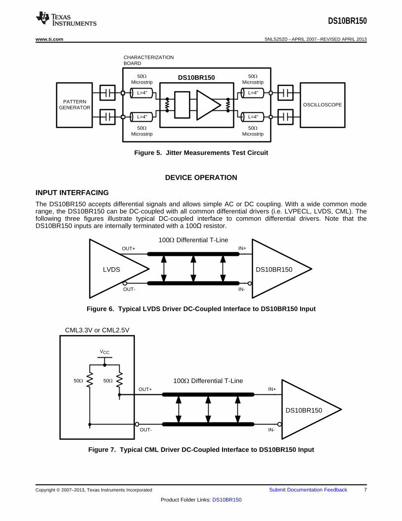
Figure 5. Jitter Measurements Test Circuit
DEVICE OPERATION
INPUT INTERFACING
The DS10BR150 accepts differential signals and allows simple AC or DC coupling. With a wide common moderange, the DS10BR150 can be DC-coupled with all common differential drivers (i.e. LVPECL, LVDS, CML). Thefollowing three figures illustrate typical DC-coupled interface to common differential drivers. Note that theDS10BR150 inputs are internally terminated with a 100Ω resistor.
Figure 6. Typical LVDS Driver DC-Coupled Interface to DS10BR150 Input
Figure 7. Typical CML Driver DC-Coupled Interface to DS10BR150 Input
Copyright © 2007–2013, Texas Instruments Incorporated Submit Documentation Feedback 7
Product Folder Links: DS10BR150

OUT+
OUT-
CML or LVPECL or LVDS
IN+
IN-
100:
100: Differential T-Line
DS10BR150
OUT+
OUT-
150-250:
100: Differential T-Line
LVDS Receiver
IN+
IN-
100:
LVPECL Driver
150-250:
DS10BR150
SNLS252D –APRIL 2007–REVISED APRIL 2013 www.ti.com
Figure 8. Typical LVPECL Driver DC-Coupled Interface to DS10BR150 Input
OUTPUT INTERFACING
The DS10BR150 outputs signals are compliant to the LVDS standard. It can be DC-coupled to most commondifferential receivers. The following figure illustrates typical DC-coupled interface to common differential receiversand assumes that the receivers have high impedance inputs. While most differential receivers have a commonmode input range that can accomodate LVDS compliant signals, it is recommended to check respectivereceiver's data sheet prior to implementing the suggested interface implementation.
Figure 9. Typical DS10BR150 Output DC-Coupled Interface to an LVDS, CML or LVPECL Receiver
8 Submit Documentation Feedback Copyright © 2007–2013, Texas Instruments Incorporated
Product Folder Links: DS10BR150

90
75
60
45
30
15
00.25 0.40 0.55 0.70 0.85 1.00
VCC = 3.3V
TA = 25°CNRZ PRBS-71062.5 Mbps
TO
TA
L R
ES
IDU
AL
JIT
TE
R (
ps)
DIFFERENTIAL INPUT VOLTAGE (V)
VICM = 1.0V
VICM = 2.4V
90
75
60
45
30
15
00.25 0.40 0.55 0.70 0.85 1.00
VCC = 3.3V
TA = 25°CNRZ PRBS-7
622 Mbps
TO
TA
L R
ES
IDU
AL
JIT
TE
R (
ps)
DIFFERENTIAL INPUT VOLTAGE (V)
VICM = 1.0V
VICM = 2.4V
DS10BR150
www.ti.com SNLS252D –APRIL 2007–REVISED APRIL 2013
Typical Performance
Figure 10. A 622 Mbps NRZ PRBS-7 Output Eye Diagram Figure 11. A 1062.5 Mbps NRZ PRBS-7 Output Eye DiagramV:100 mV / DIV, H:200 ps / DIV V:100 mV / DIV, H:150 ps / DIV
Figure 12. Total Jitter as a Function of Input Amplitude Figure 13. Total Jitter as a Function of Input Amplitude
Copyright © 2007–2013, Texas Instruments Incorporated Submit Documentation Feedback 9
Product Folder Links: DS10BR150

DS10BR150
SNLS252D –APRIL 2007–REVISED APRIL 2013 www.ti.com
REVISION HISTORY
Changes from Revision C (April 2013) to Revision D Page
• Changed layout of National Data Sheet to TI format ............................................................................................................ 9
10 Submit Documentation Feedback Copyright © 2007–2013, Texas Instruments Incorporated
Product Folder Links: DS10BR150
PACKAGE OPTION ADDENDUM
www.ti.com 10-Dec-2020
Addendum-Page 1
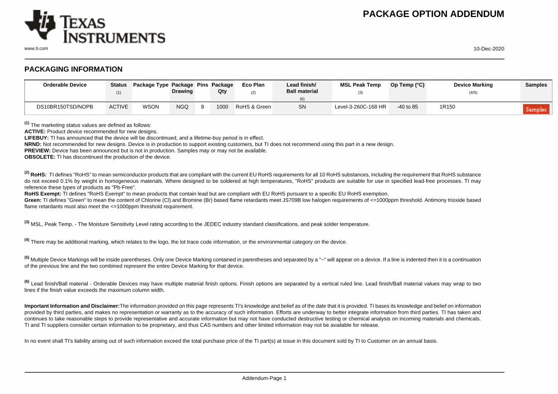
PACKAGING INFORMATION
Orderable Device Status(1)
Package Type PackageDrawing
Pins PackageQty
Eco Plan(2)
Lead finish/Ball material
(6)
MSL Peak Temp(3)
Op Temp (°C) Device Marking(4/5)
Samples
DS10BR150TSD/NOPB ACTIVE WSON NGQ 8 1000 RoHS & Green SN Level-3-260C-168 HR -40 to 85 1R150
(1) The marketing status values are defined as follows:ACTIVE: Product device recommended for new designs.LIFEBUY: TI has announced that the device will be discontinued, and a lifetime-buy period is in effect.NRND: Not recommended for new designs. Device is in production to support existing customers, but TI does not recommend using this part in a new design.PREVIEW: Device has been announced but is not in production. Samples may or may not be available.OBSOLETE: TI has discontinued the production of the device.
(2) RoHS: TI defines "RoHS" to mean semiconductor products that are compliant with the current EU RoHS requirements for all 10 RoHS substances, including the requirement that RoHS substancedo not exceed 0.1% by weight in homogeneous materials. Where designed to be soldered at high temperatures, "RoHS" products are suitable for use in specified lead-free processes. TI mayreference these types of products as "Pb-Free".RoHS Exempt: TI defines "RoHS Exempt" to mean products that contain lead but are compliant with EU RoHS pursuant to a specific EU RoHS exemption.Green: TI defines "Green" to mean the content of Chlorine (Cl) and Bromine (Br) based flame retardants meet JS709B low halogen requirements of <=1000ppm threshold. Antimony trioxide basedflame retardants must also meet the <=1000ppm threshold requirement.
(3) MSL, Peak Temp. - The Moisture Sensitivity Level rating according to the JEDEC industry standard classifications, and peak solder temperature.
(4) There may be additional marking, which relates to the logo, the lot trace code information, or the environmental category on the device.
(5) Multiple Device Markings will be inside parentheses. Only one Device Marking contained in parentheses and separated by a "~" will appear on a device. If a line is indented then it is a continuationof the previous line and the two combined represent the entire Device Marking for that device.
(6) Lead finish/Ball material - Orderable Devices may have multiple material finish options. Finish options are separated by a vertical ruled line. Lead finish/Ball material values may wrap to twolines if the finish value exceeds the maximum column width.
Important Information and Disclaimer:The information provided on this page represents TI's knowledge and belief as of the date that it is provided. TI bases its knowledge and belief on informationprovided by third parties, and makes no representation or warranty as to the accuracy of such information. Efforts are underway to better integrate information from third parties. TI has taken andcontinues to take reasonable steps to provide representative and accurate information but may not have conducted destructive testing or chemical analysis on incoming materials and chemicals.TI and TI suppliers consider certain information to be proprietary, and thus CAS numbers and other limited information may not be available for release.
In no event shall TI's liability arising out of such information exceed the total purchase price of the TI part(s) at issue in this document sold by TI to Customer on an annual basis.

TAPE AND REEL INFORMATION
*All dimensions are nominal
Device PackageType
PackageDrawing
Pins SPQ ReelDiameter
(mm)
ReelWidth
W1 (mm)
A0(mm)
B0(mm)
K0(mm)
P1(mm)
W(mm)
Pin1Quadrant
DS10BR150TSD/NOPB WSON NGQ 8 1000 178.0 12.4 3.3 3.3 1.0 8.0 12.0 Q1
PACKAGE MATERIALS INFORMATION
www.ti.com 30-Oct-2021
Pack Materials-Page 1
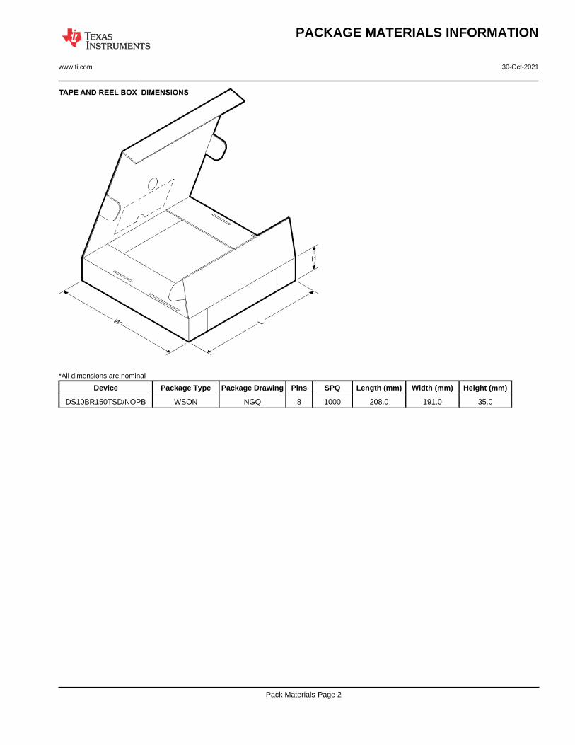
*All dimensions are nominal
Device Package Type Package Drawing Pins SPQ Length (mm) Width (mm) Height (mm)
DS10BR150TSD/NOPB WSON NGQ 8 1000 208.0 191.0 35.0
PACKAGE MATERIALS INFORMATION
www.ti.com 30-Oct-2021
Pack Materials-Page 2
www.ti.com
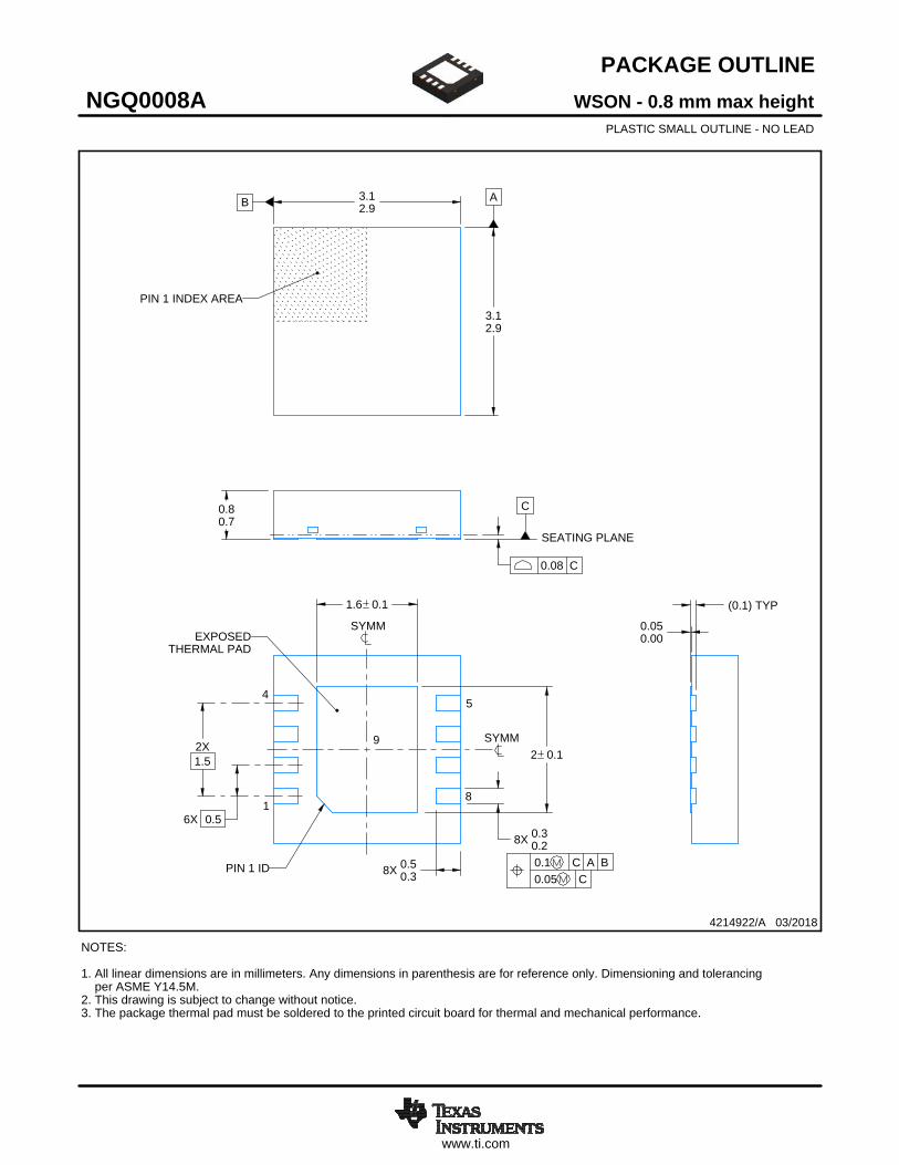
PACKAGE OUTLINE
C
8X 0.30.2
2 0.1
8X 0.50.3
2X1.5
1.6 0.1
6X 0.5
0.80.7
0.050.00
B 3.12.9
A
3.12.9
(0.1) TYP
WSON - 0.8 mm max heightNGQ0008APLASTIC SMALL OUTLINE - NO LEAD
4214922/A 03/2018
PIN 1 INDEX AREA
SEATING PLANE
0.08 C
1
45
8
PIN 1 ID 0.1 C A B0.05 C
THERMAL PADEXPOSED
9
SYMM
SYMM
NOTES: 1. All linear dimensions are in millimeters. Any dimensions in parenthesis are for reference only. Dimensioning and tolerancing per ASME Y14.5M. 2. This drawing is subject to change without notice. 3. The package thermal pad must be soldered to the printed circuit board for thermal and mechanical performance.
SCALE 4.000

www.ti.com
EXAMPLE BOARD LAYOUT
0.07 MINALL AROUND
0.07 MAXALL AROUND
(1.6)
6X (0.5)
(2.8)
8X (0.25)
8X (0.6)
(2)
(R0.05) TYP ( 0.2) VIATYP
(0.75)
WSON - 0.8 mm max heightNGQ0008APLASTIC SMALL OUTLINE - NO LEAD
4214922/A 03/2018
SYMM
1
45
8
SYMM
LAND PATTERN EXAMPLEEXPOSED METAL SHOWN
SCALE:20X
9
NOTES: (continued) 4. This package is designed to be soldered to a thermal pad on the board. For more information, see Texas Instruments literature number SLUA271 (www.ti.com/lit/slua271).5. Vias are optional depending on application, refer to device data sheet. If any vias are implemented, refer to their locations shown on this view. It is recommended that vias under paste be filled, plugged or tented.
SOLDER MASKOPENINGSOLDER MASK
METAL UNDER
SOLDER MASKDEFINED
EXPOSED METAL
METALSOLDER MASKOPENING
SOLDER MASK DETAILS
NON SOLDER MASKDEFINED
(PREFERRED)
EXPOSED METAL

www.ti.com
EXAMPLE STENCIL DESIGN
8X (0.25)
8X (0.6)
6X (0.5)
(1.79)
(1.47)
(2.8)
(R0.05) TYP
WSON - 0.8 mm max heightNGQ0008APLASTIC SMALL OUTLINE - NO LEAD
4214922/A 03/2018
NOTES: (continued) 6. Laser cutting apertures with trapezoidal walls and rounded corners may offer better paste release. IPC-7525 may have alternate design recommendations.
SOLDER PASTE EXAMPLEBASED ON 0.1 mm THICK STENCIL
EXPOSED PAD 9:
82% PRINTED SOLDER COVERAGE BY AREA UNDER PACKAGESCALE:20X
SYMM
1
45
8
SYMM
METALTYP
9

IMPORTANT NOTICE AND DISCLAIMERTI PROVIDES TECHNICAL AND RELIABILITY DATA (INCLUDING DATA SHEETS), DESIGN RESOURCES (INCLUDING REFERENCE DESIGNS), APPLICATION OR OTHER DESIGN ADVICE, WEB TOOLS, SAFETY INFORMATION, AND OTHER RESOURCES “AS IS” AND WITH ALL FAULTS, AND DISCLAIMS ALL WARRANTIES, EXPRESS AND IMPLIED, INCLUDING WITHOUT LIMITATION ANY IMPLIED WARRANTIES OF MERCHANTABILITY, FITNESS FOR A PARTICULAR PURPOSE OR NON-INFRINGEMENT OF THIRD PARTY INTELLECTUAL PROPERTY RIGHTS.These resources are intended for skilled developers designing with TI products. You are solely responsible for (1) selecting the appropriate TI products for your application, (2) designing, validating and testing your application, and (3) ensuring your application meets applicable standards, and any other safety, security, regulatory or other requirements.These resources are subject to change without notice. TI grants you permission to use these resources only for development of an application that uses the TI products described in the resource. Other reproduction and display of these resources is prohibited. No license is granted to any other TI intellectual property right or to any third party intellectual property right. TI disclaims responsibility for, and you will fully indemnify TI and its representatives against, any claims, damages, costs, losses, and liabilities arising out of your use of these resources.TI’s products are provided subject to TI’s Terms of Sale or other applicable terms available either on ti.com or provided in conjunction with such TI products. TI’s provision of these resources does not expand or otherwise alter TI’s applicable warranties or warranty disclaimers for TI products.TI objects to and rejects any additional or different terms you may have proposed. IMPORTANT NOTICE
Mailing Address: Texas Instruments, Post Office Box 655303, Dallas, Texas 75265Copyright © 2021, Texas Instruments Incorporated