DOCTORAL FELLOWSHIP PROGRAM American Society … iifillec department of the navy 0 naval research...
35
IIFILLEC DEPARTMENT OF THE NAVY NAVAL RESEARCH LASORATORY 0 WASHINGTON. D.C. 20375-5000 IN REPLY REFER TO: ONT POST DOCTORAL FELLOWSHIP PROGRAM Administered by the vow American Society for Engineering Education LO TIC for the Office of Naval Technology g LECTE ALAN KAHN O 12 198 Final Technical Report SE 15 October 87 - 15 October 88 % # 4k Ion Assisted Deposition of Fiber Coatings for Ceramic Matrix Composites with Low Dielectric Loss Tangents Overview The research for thi project has yielded significant O progress in the past year. -'rhe preliminary goal of achieving C\J facility in the growth and characterization of thin amorphous silver nitride films was reached without difficulty. Thermal annealing studies resulted in the discovery of both bubble formation and crystallization in the film These novel phenomenon were investigated further. As anticipated in the project proposal this research can -nt. ally- be divided into three segments. First is the fabrication of the amorphous films themselves. Second, the thermal stability of the films on various substrates would be investigated. Thirdly, the knowledge obtained about the structure and proper'-of the material would be utilized in understanding and further refining the science of thin film deposition. These divisions were reflected finally in the preparation of three publications' which together comprise a ' Ir complete record of the progress made this past year. The three ~2R " F,,. Av .VC4L 10 1 2
-
Upload
vuongtuyen -
Category
Documents
-
view
214 -
download
0
Transcript of DOCTORAL FELLOWSHIP PROGRAM American Society … iifillec department of the navy 0 naval research...

IIFILLECDEPARTMENT OF THE NAVY
NAVAL RESEARCH LASORATORY0 WASHINGTON. D.C. 20375-5000 IN REPLY REFER TO:
ONT POST DOCTORAL FELLOWSHIP PROGRAMAdministered by the vow
American Society for Engineering Education LO TICfor the
Office of Naval Technology g LECTE
ALAN KAHN O 12 198Final Technical Report
SE15 October 87 - 15 October 88 % # 4k
Ion Assisted Deposition of Fiber Coatings for CeramicMatrix Composites with Low Dielectric Loss Tangents
Overview
The research for thi project has yielded significant
O progress in the past year. -'rhe preliminary goal of achieving
C\J facility in the growth and characterization of thin amorphous
silver nitride films was reached without difficulty. Thermal
annealing studies resulted in the discovery of both bubble
formation and crystallization in the film These novel
phenomenon were investigated further.
As anticipated in the project proposal this research can
-nt. ally- be divided into three segments. First is the
fabrication of the amorphous films themselves. Second, the
thermal stability of the films on various substrates would be
investigated. Thirdly, the knowledge obtained about the
structure and proper'-of the material would be utilized in
understanding and further refining the science of thin film
deposition. These divisions were reflected finally in the
preparation of three publications' which together comprise a' Ir
complete record of the progress made this past year. The three
~2R "F,,. Av .VC4L 10 1 2

papers are included here.
The first paper is entitled-Near Infrared Rugate Filter
Fabrication by Ion Beam Assisted Deposition of Si(l-x)N' Films.
It has been submitted for publication to the_ journal Applied
Optics. ' 'he major emphasis of this paper is on the optical
properties of the films. It nevertheless includes an excellent
description of the work done to fabricate silicon nitrite films.
The experimental system i4, presented and the procedure used to
predict the film compositi6n from the experimental parameters is
outlined. Certain features of the film's physical and mechanical/properties are discussed/
The second jp-apt-r was submitted for publication in the
journal Nuclear Instruments and Methods B and is entitled Thermal
j.4tabilitv of Silicon Nitride Coatings Produced by Ion Assisted
Deposition,. The properties of the film both as deposited and
after annealing are discussed. Rutherford backscattering,
infrared spectroscopy, electron microscopy and X-ray diffraction
were used to characterize the samples. While none of the films
seemed to have diffused into the substrate after annealing,
blistering and crystallization did occur in certain samples
indicating inherent limitations of this material for fiber
coating applications.
The morphology of silicon nitride crystallization in the
film was investigated further. The occurrence of both Li
spherulitic and fractal aggregates in the crystallized films was.-
discovered. This fact showed the amorphous film system to be
very interesting from a crystallographic viewpoint. The growth
\ / AD [

and morphology oft.he crystal aggregate was indicative of the
interplay between atom el diffusion, impurity concentration and
competing mechanisms for crystallization. As a result of these
studies it seems possible that film stability at high
temperatures could be produced if impurities such as copper were
eliminated and the stoichiometry of the films was more carefully
controlled. THese studies are presented in the paper-Fractal and
Spherulitic Morphology of Silicon Nitride Crystallized from
Amorphous Films. which was submitted for publication to Physical
Review Letters.
ti

Near Infrared Rugate Filter Fabrication by Ion Beam Assisted Deposition of
Si(lx)Nx Films
E.P. Donovan, D. Van Vechten, A.D.F. Kahn, C.A. Carosella, and G.K. Hubler
ABSTRACT
The near infrared refractive index of amorphous silicon nitrogen alloy
films decreases continuously as the composition varies from pure silicon to
stoichiometric silicon nitride (Si3N4). Homogeneous and inhomogeneous films
up to five micrometers in thickness have been produced by simultaneous
deposition of ion beam nitrogen and electron beam evaporated silicon. Film
properties include environmental stability, resistance to chemical attack,
high hardness, thermal stability and adherence to the substrate. Film index
of refraction depends upon the relative fluxes of beam and evaporant. Band
rejection filters of the rugate design were fabricated in which the index was
sinusoidally varied with depth.
E.P. Donovan, C.A. Carosella, and G.K. Hubler : U.S. Naval Research
Laboratory, Code 4671, Wash., D.C. 20375
D. Van Vechten : Sachs Freeman Associates, NRL, Code 4671, Wash., D.C. 20375
A.D.F. Kahn Office of Naval Technology Fellow, NRL, Code 4671, Wash., D.C.
20375

2
Introduction
The term "Rugate" is descriptive both of the corrugated, sine-wave,
refractive index depth profile of the single rejection band filter and of the
desired film ruggedness against environmental stresses. The design can be
understood as a variation of the quarter wave dielectric stack. There,
layers of pairs composed of 1) high index (nH) material of thickness 1/4nH,
and 2) low index (nL) material of thickness A/4nL are sequentially deposited
on i substrate of index ns. For light of wavelength A at normal iliidence,
the reflectivity in air for M such layer pairs with no absorption is (1]
R - (l-nS(nL/nH)2M)/(l+nS(nL/nH)2M)2 -l-4ns(nL/nH) 2M (1)
where the approximation is true for small (nL/nH)2M . High reflectivity with
few layer pairs requires a large difference in index, and implies quite
different compositions, crystal structures, and thermal expansions between
the two layer materials. Interlamellar delamination is a problem under
thermal cycling for the quarter wave stack whose layer pairs differ in
thermal expansion.
The simple rugate filter [2] consists of layers whose indices of
refraction follow a sine wave cycle. The index oscillates around the average
index no with an amplitude An/2 with period 21/4no-i/2n o . In model
calculations the reflectivity at A increases as the number of cycle layers
increases at a given An, and for larger An at a set number of cycles [3].
The index profile for a multi-line rejection filter is obtained by summation
of the sinusoid for each line since the principle of superposition applies.
A rugate filter material which retains its structure through the range of An

i
3
should greatly reduce the probability for interlamellar delamination and be
more rugged than the quarter wave stack.
The fabrication method for filters must produce environmentally stable
films. Conventional vacuum deposition techniques produce films subject to
several faults. These includir igh internal stress, poor adhesion to the
substrate, and high porosity which causes irreversible and unpredictable
index changes when exposed to humid air. In many materials, a beam of
energetic particles incident upon a film during deposition improves optical,
structural, mechanical and other properties of the film [4). For example,
internal stress was relieved in germanium films evaporated with an Argon ion
beam assist, provided that an energy dependent minimum arrival rate ratio of
ions to evaporant atoms was exceeded [5]. Computer simulation showed that
the energy dependence could be understood in terms of the spatial (not
temporal) overlap of the collision cascades generated as the ions come to
rest (6]. Film stress relief thus occurs when each film atom has at least
one opportunity to change position. Generalization of this analysis to the
nitrogen IBAD of silicon process indicated that the critical arrival ratio to
produce low-stress films is far exceeded during rugate production. Thus
rugate filters fabricated by IBAD should be superior to filters fabricated by
evaporation.
In this paper we attempt to demonstrate that nitrogen ion beam assisted
deposition of amorphous silicon nitrogen alloy films is a useful technique
for the production of rugged near infrared rugate filters.
Experimental
Typical base pressure of the cryopumped bell-jar deposition chamber

4
(Figure 1) is 4xlO 5 Pa without baking. Pressure is maintained at 0.0266 Pa
during operation of the ion source. An alignment system ensures that the ion
beam can be centered on the sample mount using three Faraday cups arranged in
an equilateral triangle around the sample. The Faraday cup design
incorporates an aperture biased by negative 100 volts to repel stray
electrons and prevent the escape of secondary electrons produced when the
ions strike the cup interior. Samples may be water cooled. Ion-source-to-
samole distance is 27 cm, and the beam has normal incidence to the substrate.
Evaporator-to-sample distance is 30 cm, 200 off sample normal. A quartz
crystal oscillator shielded from the beam is used for evaporant rate control
(usually 0.5-1.0 nm/sec silicon deposition rate). A personal computer
monitors the evaporation controller and the current integrator, and controls
the ion source-beam voltage (500 eV) and extracted current (3-40 mA) during
deposition. Pure silicon substrates cut from silicon wafers were sputter
cleaned with nitrogen prior to deposition. The dose for sputtering was
sufficient to make the near surface layer amorphous, which should remove
substrate orientation effects. The usual practice was to mount a back-
roughened substrate for reflection measurements next to a doubly polished one
for transmission measurements. Some homogeneous films were deposited on
graphite, glass, quartz and alumina substrates with good substrate adhesion.
Homogeneous film compositions were measured by Rutherford backscattering
spectroscopy (RBS) [7) and analyzed using the Cornell University program [8].
Reflection and transmission spectra were measured on the Perkin-Elmer Lambda9
Spectrometer. Refractive indices were determined from fits to the reflection
interference spectra based on multi-layer calculation methods described in

5
the text by Heavens [9]. Index values quoted in this paper are those at 6000
cm-1 in wave number. The rugate filters were typically annealed at 750 C in
an argon atmosphere to reduce absorption.
Rugate Fabrication by Ion Implantation
Ion implantation of nitrogen into crystalline silicon substrates, held
at elevated temperatures to remain crystalline, was found to change the
refractive index of the implanted layer [10]. The index profiles were
determined from fits to infrared reflection spectra and were correlated with
the composition profile measured by RBS. The index at 1000 cm "1 varied in a
monotonic fashion with atom fraction of nitrogen xN, from 3.6 for pure
silicon to 3.3 at xN-O.18 to 2.1 at xN-0. 52 .
A rugate-like structure was fabricated by ion implantation at three
energies, chosen so that the peaks in the Gaussian-like distribution around
the most probable stopping distances (Rp, the projected range) provided the
varying composition profile (11]. This filter had a peak reflection of 88%.
Ion implantation was found to be impractical as a fabrication method for
rugate filters for the following reasons: 1) the maximum thickness was
limited by the projected range Rp in silicon of the maximum energy of the
nitrogen ion accelerator, 2) the width of the statistical distribution about
Rp increases with increasing energy, which prevents precise control of the
profile, and 3) available beam currents were too low for a production
process. High-current, low-energy ion sources make possible thick rugate
film fabrication by simultaneous beam and evaporant deposition.
Homogeneous Films
1 m .Immmmm m m mmm mmmmM mmlm mmm .OWN"m

6
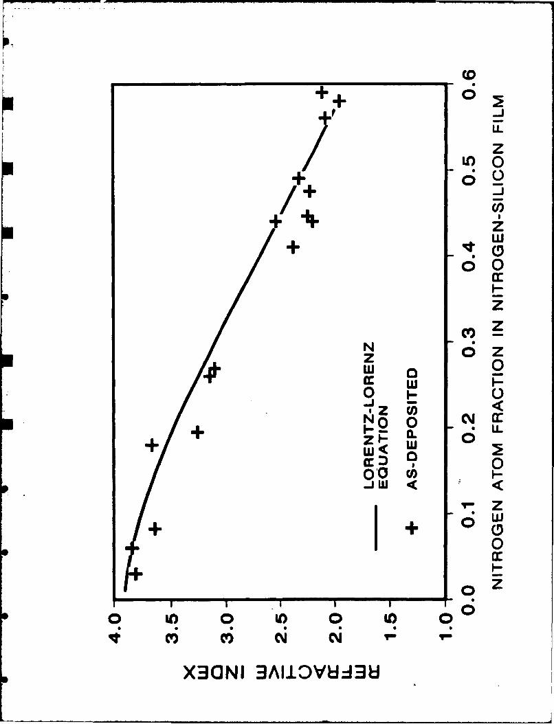
The amorphous silicon-nitrogen alloy system has been found to have a
composition dependence of the index of refraction at 6000 cm-I [12,13].
Figure 2 shows index vs. composition data for amorphous films as-deposited on
silicon substrates that remained <100 C in temperature during deposition.
The index, as a bulk property, should not depend on beam energy, so samples
from three beam energies are included. The line is a calculation using the
Lorentz-Lorenz equation, under the assumption that
PSi(I-x)Nx - PSi - x * (Psi - PSi 3N4 )/(4/7 ) (2)
where property PA denotes the density or the polarization of material A.
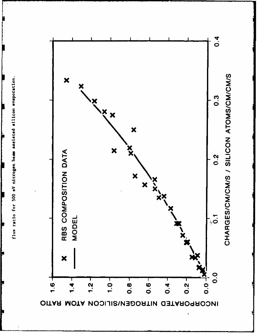
The ratio of nitrogen to silicon as measured by RBS of deposited films
as a function of the ratio Rin of the Faraday cup current density
(charges/cm2/sec) to silicon deposition rate (atoms/cm2/sec) is illustrated
in Fig. 3. The curve in Figure 3 extrapolates to .008 atom fraction of
nitrogen at zero beam current, which implies that nitrogen incorporation from
the ambient is insignificant at least at low current at the operating
pressure. The slope is approximately three, a result of several factors.
These include: 1) predominance of molecular ions relative to atomic ions
[14]; 2) charge exchange neutralization of a significant fraction of the beam
(14]; 3) backscattering of ions from the surface; and 4) sputtering of
silicon from the surface, which also causes the curve to be non-linear.
Although understanding of the overall shape of the curve is straightforward,
interpretation of the specific values and reasons for scatter is the subject
of other publications (12,13,15].
The incremental film thickness for a particular Rin should be related to
7
the incremental silicon deposit, if the sputtering, alloy composition, and
alloy density are taken into proper account. Homogeneous film thicknesses
were determined from surface profilometry, RBS, and fits to infrared spectra.
The RBS determination is at present inconsistent with the other methods.
Experiments are planned to determine whether assumptions about the density of
the films and energy loss of the analyzing beam in the films are in error.
Some scatter in the data is also believed to be caused by shifts in the non-
water cooled beam-extraction grids during deposition. For historical
reasons, the RBS determinations were used as input to the rugate filter
fabrication program.
High film purity has been achieved using our nitrogen IBAD of silicon
process. For the films with xN > 0.08, oxygen and carbon content in the film
bulk is less than the x-ray photoelectron spectroscopy detection limit of
0.01, and hydrogen content is less than 0.01 as measured by elastic recoil
detection. In a chamber with higher base pressure, a "silicon" film
depcsited simultaneously with an IBAD film but shielded from the nitrogen
beam contained twenty atomic percent oxygen and little nitrogen. Thus, the
ion beam injects nitrogen into the substrate and either removes adsorbed
oxygen, or produces a dense deposit which prevents oxygen incorporation upon
removal from the chamber.
Experiments are in progress to test film hardness, resistance to
chemical attack, wear properties, and adhesion prior to and following high
temperature anneals. Results will be reported in future publications.
Preliminary findings for slightly nitrogen deficient Si3N4 include the
following. Knoop hardness (10 gram load) is greater than three times
hardness of silicon; films adhere despite >1200 C anneal (Scotch tape test,

8
ultrasonic cleaning); etching by mixtures of hydrofluoric and nitric acids is
much slower than for CVD silicon nitride. Studies of nucleation and growth
of the crystalline phases are also underway.
Filter Fabrication
Fabrication of a rugate filter requires good control of the index vs.
thickness through the experimentally accessible parameters. Information flow
to nd from the control computer is illustrated in figure 1. The model
curves of Figures 2 and 3 were used to convert from the current-to-
deposition-rate ratio to refractive index, and RBS determinations to convert
from the ratio and incremental silicon thickness to alloy thickness. The
beam current was normally changed about once per 1.5 nm of deposited silicon,
with other variables such as beam voltage, evaporation rate set point and
chamber pressure held constant.
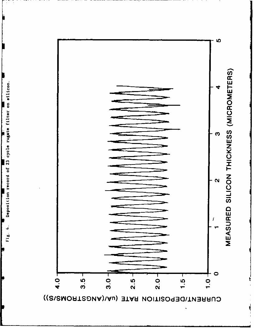
A number of rugate filters have been fabricated with peak reflections in
the i to 3 micrometer range. A twenty-three cycle Si(l-x)Nx rugate whose
deposition record is found in Figure 4 represents the largest number of
cycles that we have produced at these wavelengths. The ratio of the total
Faraday cup current in microamps to the quartz monitor indicated silicon
deposition rate in Angstroms/sec, is plotted versus the integrated silicon
deposition. The abscissa is related to Rin through the electronic charge,
the density of silicon and the Faraday cup aperture area, 0.14 cm2 . During
the deposition, the quartz monitor was subject to large instantaneous
fluctuations in indicated rate, which account for the sharp features of the
deposition record. After a thermal anneal for 30 minutes at 750 C, the
transmission spectrum was taken, and is plotted in Figure 5 as (-
9
log(transmission)) vs wavelength (micrometers). The optical density at
A-1.15 micrometers is 2.6, with AA/A-.08 (full width, half maximum of optical
density). The long wavelength range is similar to the interference pattern
that would be obtained with a homogeneous film of the same average index on
silicon. The short wavelength region is dominated by absorption in the
underlying silicon substrate. The fabrication method is clearly successful.
A theoretical transmission spectrum was calculated from the actual
dep6sition record and the data of figures 2 and 3 and is included for
illustrative purposes. Since the RBS determinations of alloy thickness have
been found inconsistent with other thickness determinations, a constant
factor was used to convert from the quartz monitor thickness of the
deposition record to the alloy thickness. The peak position is sensitive
only to the product of the cycle thickness and the average refractive index.
In the calculation, absorption was not taken into account, so the calculated
curve of Figure 5 deviates from the measured spectrum at short wavelengths.
The calculated peak optical density is only 0.2 larger than the measured
value for the sample of Figure 5, which gives confidence that rugate filters
with larger numbers of cycles should yield higher optical density.
Summary
In conclusion, nitrogen ion-beam-assisted deposition of silicon has been
shown to be a practical method for deposition of rugate filters upon silicon
substrates. Quartz monitor control on the deposition with dynamic computer
control of the Faraday cup current to produce sinusoidal index variation with
depth is adequate to make infrared filters with high optical densities. The
filters have excellent mechanical, thermal, and chemical stability, and

10
adhere to the silicon substrates despite anneals up to 1200 C.
11
References
1. E.Hecht and A.Zajak, Optics, Addison Wesley, Reading, MA (1979)
2. C. Strecker, W. Johnson, and J. Davison "The Preparation of a SiGe
Rugate Variable Index Optical film by a Solid State Diffusion Process"
AFWAL-TR-85-4087 (1985)
3. G.K. Hubler, E.P. Donovan, D. Van Vechten, R.H. Bassel and D.R.
Brighton, "Ion Beam Assisted Deposition of Optical Coatings" NRL
Memorandum Report 5927, 1987.
4. S.M. Rossnagel, and J.J. Cuomo, MRS Bulletin 12 (1987) 40-49
5. E.H. Hirsh and I.K. Varga, " Thin Film Annealing by Ion Bombardment"
Thin Solid Films, 69, 99 (1980).
6. D.R. Brighton, and G.K. Hubler "Binary Collision Cascade Prediction of
Critical Ion-To-Atom Arrival Ratio in the Production of Thin Films With
Reduced Intrinsic Stress" Nucl. Inst. And Meth. B28 (1987) 527
7. See, for example, W.K. Chu, J.M. Mayer, and M. Nicolet, Backscattering
Spectroscopy, Academic Press, New York (1978)
8. L.R. Doolittle, "Algorithms for the Rapid Simulation of Rutherford
Backscattering Spectra" Nucl. Instr. and Methods B9 (1985) 344
9. 0. Heavens, Optical Properties of Thin Solid Films Dover Publications,
New York,NY (1965)
10. G.K. Hubler, P.R. Malmberg, and T.P. Smith, III, "Refractive Index
Profiles and Range Distributions of Silicon Implanted with High-Energy
Nitrogen" J. Appl. Phys. 50 (1979) 7147
11. G.K. Hubler, P.R. Malmberg, and T.P. Smith III, "Ion-Implanted
Multilayer Optical Interference Filter" Patent #4,262,056 (1981)
12. E.P. Donovan, D.R. Brighton, G.K. Hubler, and D. Van Vechten, "Ion Beam

12
Assisted Deposition of Substoichiometric Silicon Nitride" Nucl. Instru.
Meth., B19/20 (1987) 983
13. E.P. Donovan, D.R. Brighton, D. Van Vechten and G.K. Hubler, "Infrared
and Ion Beam Analysis of SixNl.x Alloys Grown by Ion Beam Assisted
Deposition" in M. Wittmer, J. Stimmell and M. Strathman, Material Issues
in Silicon Integrated Circuit Processing. Materials Research Society,
Pittsburgh,PA (1986) 487
14.' D. Van Vechten, G.K. Hubler, and E.P. Donovan, "Characterization of a 3
cm Kaufman Ion Source with Nitrogen Feed Gas" Vac. Technol. Appl. & Ion
Physics a (1986) 841
15. D. Van Vechten, G.K. Hubler, and E.P. Donovan, "Summary Abstract:
Factors Important to Achieving Compositional Control and Reproducibility
in a Reactive Ion Beam Assisted Deposition Process" J. Vac. Sci. and
Tech. (1988)

13
Fig. 1. Schematic diagram of ion beam assisted deposition (IBAD) system.
1) Electron beam evaporator with silicon charge. 2) Kaufman ion
source with nitrogen feed gas. 3) Faraday cups with secondary
electron suppression. 4) Quartz crystal evaporation monitor.
Fig. 2. Refractive index at 6000 cm"1 vs. nitrogen atom fraction in as-
deposited films.
Fig. 3. Film nitrogen to silicon ratio vs. Rin, incident charge-to-silicon
flux ratio for 500 eV nitrogen beam assisted silicon evaporation.
Fig. 4. Deposition record of 23 cycle rugate filter on silicon.
Fig. 5. (-loglo(transmission)) vs. wavelength for rugate filter of Figure 4
after 750 C anneal. Absorption in substrate occurs at low
wavelengths.

Fig. I. Schematic diagram of ion beam assisted deposition (IRAD) system.
1) Electron beam evaporator with silicon charge. 2) Kaufman ion
source with nitrogen feed gas. 3) Faraday cups with secondary
electron suppression. 4) Quartz crystal evaporation monitor.
INFORMATIONFLOW
ION SOURCEPOWER SUPPLY
CURRENT 3\INTEGRATOR
COMPUTER//I
QUARTZ 'CRYO-MONITOR & PUMP
CONTROLLER
ELECTRON BEAM VACUUM
POWER SUPPLY CHAMBER
o60
z
0 P0z Fo <
z0
0'a-J
+ + oa:DO 0
0 z
0 ) 1 0 0 to 00
X30NI 3AUSDVU:13U
Cl)
o x0.0
xx
o00
01 x
xxx-4 0 x C
00
0.04, x
0 0
p Iw a
w00
wUz
00100
w--
0 c
CO)I.' w
*6 z C((/Y0ULD V/n .Lk O.l~3/NWn

CC
00 "'0
bo .
-4jo c0
do 0
~ .0
6 C
4
*ISN3 -4-I~

THERMAL STABILITY OF SILICON NITRIDE COATINGS PRODUCED BY ION ASSISTEDDEPOSITION
K.S. Grabovski, A.D.F. Kahn, 3.P. Donovan, C.A. CarosellaCode 4671, Naval Research Laboratory, Washington, DC 20375
Amorphous Si-N alloy films containing from about 20 to 60 at. % N weredeposited by combined o-beau evaporation of Si and ion bombardment ofN. A Kaufman-type ion gun produced the 500-eV nitrogen ion beam.Films up to I-om thick were deposited on single-crystals of siliconand sapphire in a vacuum of about 2xlO"4 torr. The as-deposited filmswere characterized by Rutherford backscattering spectroscopy forcomposition, visible and near-infrared spectrophotometry to measureindex of refraction and absorption bands from Si-N bond vibrations,and X-ray diffraction for crystal structure. Subsequently, samplesw4re annealed in a thermogravinetric analyzer at temperatures up to1350 0 C to ascertain their thermal stability against crystallization,oxidation, and reaction with the substrate. Postanneal examination byRutherford backscattering, spectrophotometry, X-ray diffraction, andoptical and scanning electron microscopy provided detailed informationon the thermally induced changes in the films. Crystallization of Sioccurred in N-poor samples, while QSi 3N4 crystallized in N-richsamples after 12000 C anneals. Blisters sometimes also appearedfollowing 12000 C anneals of N-rich samples. For anneals up to 12000C,no reactions with sapphire or Si substrates were observed and minimaloxidation was found.
DRAFT COPY
Presented at IBMH 88Tokyo, Japan

1. INTRODUCTION
Previously Donovan et al. (1-31 have developed the ion assisted
deposition (IAD) technique for making Si-N alloy films of uniform
composition up to 1 pa thick. They were able to continuously vary the N
content in the films from 0 to 63 at. % N. Such films were found to be
amorphous, dense, corrosion resistant, and adherent to single crystal Si
substrates. Evidence of film structural relaxation was found after a 2h
ann.al at 9000C for films containing up to about 20 at. % N (1,3].
This work addresses the thermal stability of IAD films containing up to
about 60 at. % N, and for annealing temperatures up to 13500 C. Single
crystal substrates of both Si and sapphire were used to evaluate possible
film/substrate interactions at these higher temperatures. Film composition,
microstructure, and optical properties were examined.
2. EXPERIMENTAL PROCEDURE
Si substrates were cut from p type, B doped <111> and <100> Si wafers.
Sapphire substrates with c <00.1>, m <10.0>, and a <11.0> plane orientations
were used in the as-received condition. Substrates were cleaned with
acetone after mounting with silver print, and sputter cleaned with the ion
beam just prior to film deposition.
Details of the film deposition equipment and procedures have been
previously described by Van Vechten et al. [4,5] and Donovan et al. [1,2].
For this work a Si evaporation rate of 0.5 nm/s was used. The N flux was
altered by changing the cathode current of a Kaufman ton source operated at
500 eV. From previous work (51 the ion beam was expected to consist of 89%
diatomic and 11% monatomic tons, plus some neutralized N. The substrates
were aimed at the ion gun. Atom arrival rate ratios of N/Si between 0.17
and 0.8 were used to produce uniform films typically 300 to 500-nm thick
containing between 17 and 60 at. % N. The substrates were maintained in a
vacuum of about 2 x 10⁻⁴ torr during film deposition.
.Film composition was determined by 2.0 MeV 4He+ + Rutherford
backscattering spectroscopy (RES) using the RUMP computer program [6].
Crystalline structure was determined by 9-20 X-ray diffraction (XRD) using
Cu K,, X-rays, a curved graphite monochromator, and a 0.125 deg/min scan
rate. The index of refraction was evaluated as a measure of film structural
relaxation using a technique described by Hubler at al. [7]. The
Restrahlen absorption bands below 1000 cm"1 showing information about Si-N
bonds [8,9] were examined using Fourier transform infrared spectrometry
(FTIR). Optical and scanning electron microscopy (SEP) were performed as
necessary.
Samples were annealed in a thermogravimetric analyzer under high purity
Ar flowing at 60 cm3/min. After insertion into the cool furnace the
temperature was increased at a rate of 40 0 C/min up to the annealing
temperature. Samples were cooled in the furnace at a rate of about 40 0 C
min, down to about 800 0 C before exposure to the atmosphere.
3. RESULTS AND DISCUSSION

Films with a N content below 20 at. % had previously exhibited
structural relaxation of Si upon annealing to 9000C for 2h (I. This was
observed by a change in the index of refraction of the deposited film.
I However, X-ray diffraction in this york of a sample containing 18 at. % N
after annealing at 9000C for 2h followed by 9500C for 0.5h revealed no
additional diffraction peaks beyond the substrate Si (111) peak.p
Films containing about 20 to 30 at. I N and deposited on Si exhibited Si
cry tallization upon annealing at 12000C for 45 minutes. Under these
conditions, randomly oriented polycrystalline Si formed as determined by
XRD. The volume fraction of crystalline Si diminished as the N content
increased. However, a nominally 30 at. % N film on a-plane sapphire and
annealed at 12000C for 45 min showed no evidence of Si crystallization, but
did show small spherulites of aSi 3N4 by optical microscopy.
The low temperature phase OSi3N4 crystallized in films on Si containing
more than about 30 at. % N but less than the stoichiometric amount (57.1 at.
1) when annealed to temperatures in excess of about 1100*C. The morphology
of the precipitates is particularly interesting, as shown in Fig. 1. While
such spherulites were previously observed in Si-N alloys formed by ion
implantation [101 , these are considerably more well formed. These
spherulites would normally be difficult to see in the optical microscope,
since crystallization only slightly changes the index of refraction of Si3N4
[11,121. However, aSi 3N4 has an hexagonal structure and is therefore
birefringent. Since the precipitates usually formed with the c axis
inclined to the sample normal, the spherulites could be viewed with
crossed polarizers in the optical microscope. In fact, the c axis was
frequently found to lie in the plane of the sample surface as shown in Fig.
2 for a sample annealed at 1200 0 C for 3 sin folloved by 12500 for lh. The
predominant peaks found by symmetric XD are all of the hkO variety. This
occured for both SL <100> and <111> orientations. Further annealing
disrupted this preferred orientation. A more detailed discussion of the
precipitate morphology and growth kinetics of the spherulLtes will be
presented elsewhere.
Another feature found after annealing films containing more than about
30 at. % N was blisters, as shown in Fig. 3. These were found on films
deposited on both sapphire and Si substrates, although they appeared to
occur more readily on sapphire substrates. The blisters formed after
annealing in excess of 11000 C and are believed to occur due to a"lomeration
of N in the film into bubbles containing N2 gas, or as a result of film
delamination from the substrate due to stress. The blisters are not
believed to form during specimen cooling since the spherulite number density
is frequently diminished in the imediate vicinity of the blisters.
For films containing a nearly stoichiometric amount of N (57.1 at. %),
no evidence of aSL 3N4 crystallization was found for films on sapphire
substrates by optical microscopy after annealing up to 12000 C for lh.
Crystallization did occur on Si substrates, usually after a 12000 C anneal,
but in one case required an anneal up to 1350 0C for lh. Perhaps excess Si
aids the nucleation process.
Very little oxidation or interaction with either the Si or sapphire
substrates was observed by PBS for films containing more than 40 at. % N
IIk: I I / - - IM

4. CONCLUSIONS
Amorphous lAD alloy films of Si and N were readily made up to the
stoichiometric composition of i3N4 . For N content between 30 and 50 at.
%, these films remained amorphous and stable up to about 1100°C for lh.
Transformations occured by Si or OSi 3N4 crystallization, and by blister
formation. Nominally stoichiometric films on sapphire and in one case on Sit
were: more resistant to crystallization, but more prone to blisger formation.
Little oxidation or interaction with substrate Si or sapphire was found for
anneals up to 12000 C.
The authors acknowledge the helpful comments of G. K. Hubler and D. Van
Vechten in the course of this work, and acknowledges the support ofjA. D. F.
i~n the U.S. Office of Naval Technology.

REFEUENCZ$
(1) 3.P. Donovan, D.R. Brighton, O.K. Hubler, and D. Van Vechten, Nucl.Instr. and Math. B19/20 (1987) 963.
121 E.P. Donovan, D. Van Vachten, A.D.F. Kahn, C.A. Carosella, and O.K.Hubler, submitted to Applied Optics.
(3] E.P. Donovan, D.R. Brighton, D. Van Vechten, and C.K. Hubler, Mater.Res. Soc. Symp. Proc. 71 (1986) 487.
[4] D. Van Vechten, C.K. Hubler, and E.P. Donovan, to be published in J.Vac. Sci. Technol. A.
(5] D. Van Vechten, G.K. Hubler, and E.P. Donovan, Vacuum 36 (1986) 841.
(6]-. L.R. Doolittle, Nucl. Instr. and Moth. B9 (1983) 344.
(7] O.K. Hubler, P.R. Malmberg, and T.P. Smith III, J. Appl. Phys. 50(1979) 7147.
[8] J.A. Borders and W. Beezhold in Ion Inmlantation in Semiconductors,eds., I. Ruge and J. Graul (Springer, Nev York, 1971) p. 241.
(9] Yu. N. Volgin and Yu. I. Ukhanov, Opt. Spectrosc./38 (1975) 412Y.
(101 J. Belz, E.H. To Kaat, C. Zimmer, and H. Vogt, Nucl. Instr. and Moth.B19/20 (1987) 279.
(111 E.A. Taft, J. Electrochem. Soc. A(1971) 1341.
(12] John T. Milek, Silicon Nitride for Microelectronic Aoolications. Part1. Preoaration and Prooerties, in series, Handbook of ElectronicMaterials, Vol. 3 (IFI-Plenum, Nov York, 1971) p. 54.

FIGURES CAPTIONS
Fig. 1. Optical micrograph of spherulites formed in nominally 30 at. % N
film deposited on Si <100> after annealing at 12000 C for 45 min.
Crossed polarizers were used to view otherwise invisible optically
active precipitate.
Fig. 2. X-ray diffraction scan for sample with more fully developed
spherulites. Reference bars are from powder data file for aSi 3 N4 .
Note the strong prevalence of hk 0-type reflections. This sample
had 54 at. % N, was on Si <100> and was annealed for 3 min at
12000C, followed by lh at 12500 C.
Fig. 3. SE photo showing blisters formed on nominally stoichiometric
S1 3 N4 film deposited on a-plane sapphire and annealed for 15 min
at 11500C. No spherulites were observed by optical microscopy.
Fig. 4. Optical micrograph series showing evolution of blisters upon
annealing of stoichiometric film on Si <100> for lh at a) 12500 C,
b) 13000 C, and c) 13500 C. The blisters rupture, allowing
oxidation of underlying Si.
Fig. 5. FTIR transmission scans with substrate Si absorption removed
showing Restrahlen absorption from Si-N bond vibrations in 49 at.
% N film on Si <100>. Broad peak is from amorphous as-deposited
sample, sharper peak with more structure is from sample after
isochronal anneals ending at 12500 C where substantial OSi 3N4
crystallization was observed.
Fig. 6. FTIR transmission scans of 49 at. % N film after 1100°C-lh anneal
where little relaxation of amorphous structure was seen, and also
of sample shown in Fig. 4c after oxide was etched away by HF acid.
Onset of Si3N4 crystallization can be seen.

C44

00 U)
400
fA4
CA.
00
00
10
0 0 0 0 0 0 0 0 00 0f 0 W) 0 W 0 0t0 0t CY 0 N. CYCM -'
,A1!suejul

L -
U
ma
C

Ile

.oI.
/I
jizzzV#NVU

4
i.
N
'K>I -
Jp.
b.
A
I
IIt
4-
/~1~
/
/ //
//
1// /
I,* I,,!,, I I VIII'.
I
(ii) MOISSIRSNWL