DLP Series-600 DMD Mechanical, Thermal, and Systems ...
39
DLP ® Series-600 DMD Mechanical, Thermal, and Systems Mounting Concepts Application Report Literature Number: DLPA053 December 2014
Transcript of DLP Series-600 DMD Mechanical, Thermal, and Systems ...

DLP® Series-600 DMD Mechanical, Thermal, andSystems Mounting Concepts
Application Report
Literature Number: DLPA053December 2014

Contents
1 Scope ................................................................................................................................. 52 Terminology ........................................................................................................................ 53 DMD Specifications .............................................................................................................. 7
3.1 Optical Interface Features............................................................................................... 73.2 DMD Cross-Section Features .......................................................................................... 83.3 Dust Gasket or System Aperture Mating Surface.................................................................... 93.4 Optical Illumination Overfill.............................................................................................. 93.5 Active Size and Location .............................................................................................. 103.6 Electrical Interface Features .......................................................................................... 113.7 Thermal Characteristics................................................................................................ 13
3.7.1 Thermal Test Points ....................................................................................... 143.7.2 Array Temperature and its Calculation ................................................................... 153.7.3 Sample Array Calculation for a Typical 1-Chip Display Application .................................. 16
3.8 Mechanical Loading .................................................................................................... 164 System DMD Mounting ....................................................................................................... 18
4.1 Critical Considerations for Mounting and Utilizing the DMD ...................................................... 184.2 Basic System DMD Mounting Concept .............................................................................. 20
4.2.1 Optical-Mechanical Alignment Features ................................................................. 224.2.2 Heat Sink Mounting ......................................................................................... 23
4.2.2.1 Direct Control of Heat Sink Mounting Loads........................................................ 234.2.2.2 Indirect Control of Heat Sink Mounting Loads ...................................................... 24
4.2.3 DMD-PCB Mounting ........................................................................................ 254.2.3.1 Direct Control of PCB Mounting Loads .............................................................. 254.2.3.2 Indirect Control of PCB Mounting Loads ............................................................ 27
4.2.4 Dust Gasket ................................................................................................. 284.2.5 System Aperture ............................................................................................ 284.2.6 System Aperture and Dust Gasket Mounting ........................................................... 29
4.3 Detailed DMD Mounting Concepts ................................................................................... 304.3.1 Edge Guide Mounting Concept ........................................................................... 30
4.3.1.1 Heat Sink Mounting .................................................................................... 314.3.1.2 PCB Mounting........................................................................................... 34
5 System Sockets ................................................................................................................. 355.1 Socket Design and Selection Considerations....................................................................... 355.2 Series-600 Socket ..................................................................................................... 37
6 Drawing and 3D-CAD File References ................................................................................... 38
2 Table of Contents DLPA053–December 2014Submit Documentation Feedback
Copyright © 2014, Texas Instruments Incorporated

www.ti.com
List of Figures1 Series-600 DMD Features – Window Side ............................................................................... 62 Series-600 DMD Features – Pin Side..................................................................................... 73 Series-600 DMD Datum Features ......................................................................................... 84 Series-600 DMD Cross Section View ..................................................................................... 95 Optical Illumination Overfill................................................................................................ 106 Active Array Location ...................................................................................................... 117 Pin Numbering Scheme ................................................................................................... 128 Electrical and Thermal Interface.......................................................................................... 139 Thermal Test Points – Standard Locations ............................................................................. 1510 DMD Mechanical Loads ................................................................................................... 1811 Basic DMD Mechanical Mounting Concept ............................................................................. 2112 Optical Interface (Alignment) Features .................................................................................. 2213 Heat Sink Mounting – Load Control by Design......................................................................... 2414 Direct Control of DMD-PCB Mounting Options......................................................................... 2615 DMD-PCB Mounting Gap - Indirect Control of Load on DMD ........................................................ 2816 System Aperture and Dust Gasket....................................................................................... 2917 DMD Mounting Concept – Edge Guide ................................................................................. 3118 Heat Sink Mounting Tolerance Analysis Schematic Diagram ........................................................ 3219 DMD-PCB Gap Analysis Schematic Diagram .......................................................................... 3420 Socket Installed Height .................................................................................................... 3621 Zero Insertion Force Style Series-600 Socket.......................................................................... 37
3DLPA053–December 2014 List of FiguresSubmit Documentation Feedback
Copyright © 2014, Texas Instruments Incorporated

www.ti.com
List of Tables1 Gap for Compression Spring ............................................................................................. 322 Analysis Summary for DMD Thermal Area Mechanical Load ........................................................ 333 Gap between Interface Boss and DMD-PCB ........................................................................... 354 Reference Drawings and 3D-CAD Models.............................................................................. 38
4 List of Tables DLPA053–December 2014Submit Documentation Feedback
Copyright © 2014, Texas Instruments Incorporated

Application ReportDLPA053–December 2014
DLP® Series-600 DMD Mechanical, Thermal, and SystemsMounting Concepts Application Report
1 ScopeThis application report serves as an aid to the successful first-time utilization and implementation of theSeries-600 DMD (DLP6500FYE) and addresses the following topics:• Terminology• Specification and design details of a Series-600 DMD• System mounting concepts for the DMD, including key attributes and important application design
considerations• Socket for use with the Series-600 DMD
2 TerminologyBTB — Board-to-Board connector; refers to a type of electrical connector that is typically used to provide
electrical connection between two PCBs, or a PCB and a FPCB
Dark Metal — area just outside the active array but within the same plane as the active array, seeFigure 5. This area is darker in color and has reduced reflectivity compared to the active array.
DMD Features— The primary features of the Series-600 DMD are described below and illustrated inFigure 1 and Figure 2• Active array – the two-dimensional array of active DMD mirrors which reflect light• Bond wires – the wires which electrically connect the WLP DMD Chip to the ceramic carrier• Ceramic carrier – the structures which form the mechanical, optical, thermal, and electrical
interfaces between the WLP DMD chip and the end-application optical assembly• Corner chamfer – visual keying and orientation aid located on the ceramic carrier. Also identifies
the incoming illumination corner• DMD Chip (or just DMD) – The aggregate of the WLP chip, ceramic carrier, bond wires,
encapsulation, and electrical pins• Electrical pins – the electrical interface between the ceramic carrier and the end-application
electronics• Encapsulation – the material used to mechanically and environmentally protect the bond wires• Symbolization pad – the area on the ceramic carrier that is used for marking the part• Thermal interface area – the area on the ceramic carrier which allows direct contact of a heat
sink or other thermal cooling device• Window glass – the clear glass cover which protects the DMD active area (mirrors)• Window aperture – the dark coating on the inside surface of the window glass around the
perimeter of the active array• WLP Chip – Wafer-Level Package (WLP) DMD chip which contains the DMD active array,
window glass, and window aperture
FPCB— Flexible Printed Circuit Board
DLP is a registered trademark of Texas Instruments.
5DLPA053–December 2014 DLP® Series-600 DMD Mechanical, Thermal, and Systems MountingConceptsSubmit Documentation Feedback
Copyright © 2014, Texas Instruments Incorporated

Window Aperture
WLP Chip
(inside window surface)
Window Glass
Encapsulation
Ceramic Carrier
Active Array
Terminology www.ti.com
Illumination Light Bundle— refers to the illumination cross-section area (size) at any location along theillumination light path but more specifically at the DMD active array and within the same plane asthe active array
Interposer— component that provides electrical connection to a DMD that utilizes a land grid array forthe system electrical connection (similar to a socket or connector)
LGA— Land Grid Array (refers to a two-dimension array of electrical contact pads)
Mechanical ICD — the Mechanical Interface Control Drawing (ICD) describes the geometriccharacteristics of the DMD. This is also referred to as the Package Mechanical Characteristics
Optical Assembly— a sub-assembly of the end-application, which consists of optical components andthe mechanical parts that support those optical components
Optical Chassis— the main mechanical part used in the optical assembly to mount the opticalcomponents (DMD, lens, prism, and others)
Optical Illumination Overfill — the optical energy that falls outside the active area, and which does notcontribute to the projected image (see Figure 5)
Optical Interface— refers to the features on the optical chassis used to align and mount the DMD
PCB— Printed Circuit Board
PGA— Pin Grid Array (refers to a two-dimensional array of electrical contact pins)
RSS — Root Sum Square method of characterizing part tolerance stack-ups. This is the square root ofthe sum of each part tolerance squared
SUM — Sum method of characterizing part tolerance stack-ups. This is the sum of each part tolerance
TP — Thermal test point
Figure 1. Series-600 DMD Features – Window Side
6 DLP® Series-600 DMD Mechanical, Thermal, and Systems Mounting DLPA053–December 2014Concepts Submit Documentation Feedback
Copyright © 2014, Texas Instruments Incorporated
Corner Chamfer(Alignment & Keying)
Symbolization Pad
Pins Missing
Electrical Pins
(Alignment & Keying
Thermal Interface Area
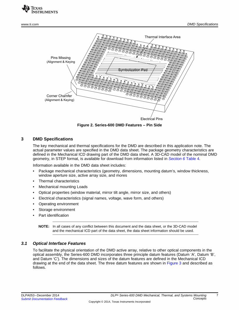
www.ti.com DMD Specifications
Figure 2. Series-600 DMD Features – Pin Side
3 DMD SpecificationsThe key mechanical and thermal specifications for the DMD are described in this application note. Theactual parameter values are specified in the DMD data sheet. The package geometry characteristics aredefined in the Mechanical ICD drawing part of the DMD data sheet. A 3D-CAD model of the nominal DMDgeometry, in STEP format, is available for download from information listed in Section 6 Table 4.
Information available in the DMD data sheet includes:• Package mechanical characteristics (geometry, dimensions, mounting datum’s, window thickness,
window aperture size, active array size, and mores• Thermal characteristics• Mechanical mounting Loads• Optical properties (window material, mirror tilt angle, mirror size, and others)• Electrical characteristics (signal names, voltage, wave form, and others)• Operating environment• Storage environment• Part identification
NOTE: In all cases of any conflict between this document and the data sheet, or the 3D-CAD modeland the mechanical ICD part of the data sheet, the data sheet information should be used.
3.1 Optical Interface FeaturesTo facilitate the physical orientation of the DMD active array, relative to other optical components in theoptical assembly, the Series-600 DMD incorporates three principle datum features (Datum ‘A’, Datum ‘B’,and Datum ‘C’). The dimensions and sizes of the datum features are defined in the Mechanical ICDdrawing at the end of the data sheet. The three datum features are shown in Figure 3 and described asfollows.
7DLPA053–December 2014 DLP® Series-600 DMD Mechanical, Thermal, and Systems MountingConceptsSubmit Documentation Feedback
Copyright © 2014, Texas Instruments Incorporated
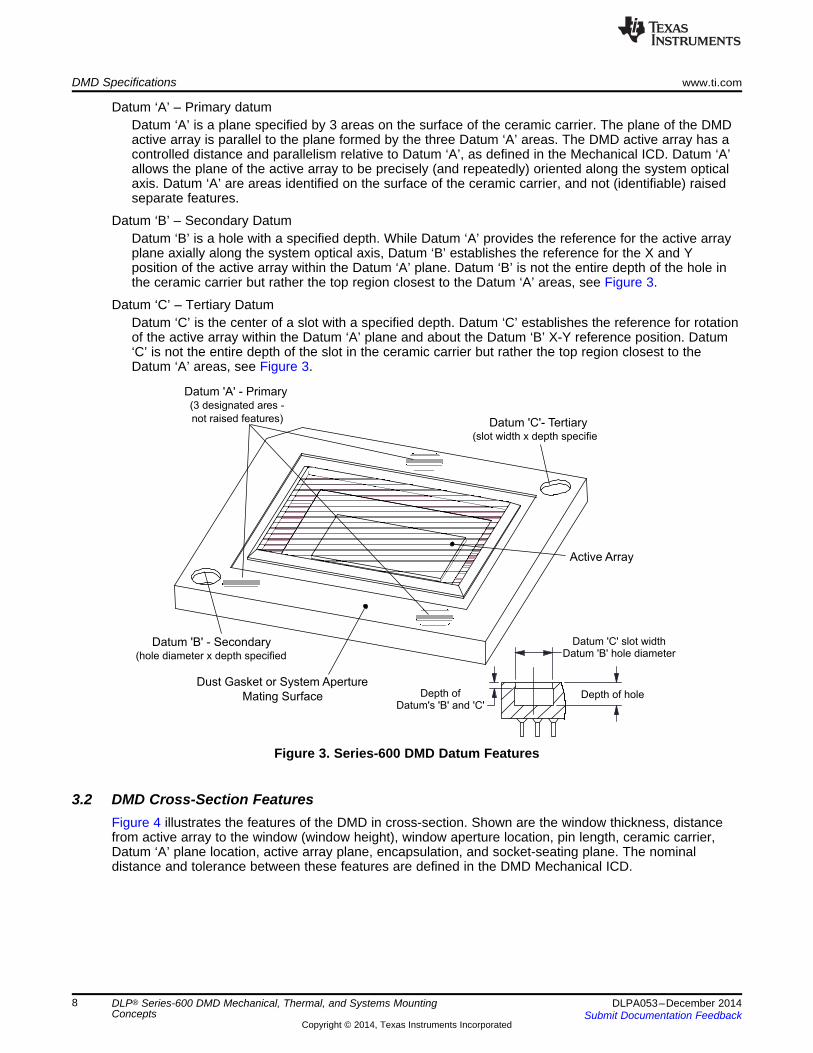
Datum 'B' - Secondary
Datum 'C'- Tertiary
Datum 'A' - Primary
(hole diameter x depth specified
(slot width x depth specifie
(3 designated ares -
not raised features)
Dust Gasket or System Aperture
Mating Surface
Datum 'C' slot widthDatum 'B' hole diameter
Depth of holeDepth ofDatum's 'B' and 'C'
Active Array
DMD Specifications www.ti.com
Datum ‘A’ – Primary datumDatum ‘A’ is a plane specified by 3 areas on the surface of the ceramic carrier. The plane of the DMDactive array is parallel to the plane formed by the three Datum ‘A’ areas. The DMD active array has acontrolled distance and parallelism relative to Datum ‘A’, as defined in the Mechanical ICD. Datum ‘A’allows the plane of the active array to be precisely (and repeatedly) oriented along the system opticalaxis. Datum ‘A’ are areas identified on the surface of the ceramic carrier, and not (identifiable) raisedseparate features.
Datum ‘B’ – Secondary DatumDatum ‘B’ is a hole with a specified depth. While Datum ‘A’ provides the reference for the active arrayplane axially along the system optical axis, Datum ‘B’ establishes the reference for the X and Yposition of the active array within the Datum ‘A’ plane. Datum ‘B’ is not the entire depth of the hole inthe ceramic carrier but rather the top region closest to the Datum ‘A’ areas, see Figure 3.
Datum ‘C’ – Tertiary DatumDatum ‘C’ is the center of a slot with a specified depth. Datum ‘C’ establishes the reference for rotationof the active array within the Datum ‘A’ plane and about the Datum ‘B’ X-Y reference position. Datum‘C’ is not the entire depth of the slot in the ceramic carrier but rather the top region closest to theDatum ‘A’ areas, see Figure 3.
Figure 3. Series-600 DMD Datum Features
3.2 DMD Cross-Section FeaturesFigure 4 illustrates the features of the DMD in cross-section. Shown are the window thickness, distancefrom active array to the window (window height), window aperture location, pin length, ceramic carrier,Datum ‘A’ plane location, active array plane, encapsulation, and socket-seating plane. The nominaldistance and tolerance between these features are defined in the DMD Mechanical ICD.
8 DLP® Series-600 DMD Mechanical, Thermal, and Systems Mounting DLPA053–December 2014Concepts Submit Documentation Feedback
Copyright © 2014, Texas Instruments Incorporated

Window Aperture Plan
Window Thickness
e
Window Height
Active Array Plane(focus or image plane)
Socket Seating Plane
Window
Encapsulation
Ceramic
Carrier
Datum 'A' to Array
Pin Length
3 Places Indicated
A
Pin Braze Fillet
www.ti.com DMD Specifications
Figure 4. Series-600 DMD Cross Section View
3.3 Dust Gasket or System Aperture Mating SurfaceAs shown in Figure 4 the exterior surface of the DMD window is relatively close to the image plane of theDMD active array. Since the DMD active array is the optical focus plane, there is a risk for any dustparticles on the outside window surface to be re-imaged and appear in the projected image. To preventthis from occurring it is best to prevent dust from getting onto the outside surface of the DMD window. Thiscan be accomplished by:• Not having any openings in the optics assembly (close openings using gaskets, tape, and so forth)• Maintain optical cleanliness of all components used in the optical assembly, including the mechanical
parts• Assemble the optical engine in a clean-room environment, including installation of the DMD• Avoid processes that could produce loose particles that could reach the DMD window
It is important that any gasket be flexible (compressive) enough that it does not interfere with contactbetween the DMD Datum ‘A’ features and the associated features on the optical chassis. Suchinterference could result in issues with optical focus uniformity.
Depending on the specific optical design there is the potential for low-level light that scatters off the opticalchassis or optical components to enter the projection pupil and be displayed in or around the projectedimage. To prevent or reduce this a system aperture could be used to block this light from entering theprojection pupil. The design of the system aperture is very dependent on each optical design and opticalchassis.
The flat area of the ceramic carrier which is generally in the same plane as Datum ‘A’, but not includingthe Datum ‘A’ areas, can provide a resting (or mating) surface for a system aperture and/or dust gasket.The system aperture or gasket should be kept clear of the Datum ‘B’, Datum ‘C’, and Datum ‘A’ areas toensure the optical alignment of the DMD is not interfered with. The surface is depicted in Figure 3.
3.4 Optical Illumination OverfillOptical illumination overfill is defined as the optical energy that falls outside the active area. Overfill iswasted light that is not reflected by the mirrors and does not contribute to the brightness of a projectedimage. The shape and spatial distribution of the optical energy in the overfill region is determined by thesystem optical design. An example overfill from an illumination profile is illustrated in Figure 5.
Typical attributes that result in different overfill profiles include (but are not limited to) integrator size,illumination source, and optical aberrations (such as distortion, or color separation, or both).
Excess optical illumination overfill can result in higher thermal loads on the DMD (which must be cooled bythe system), or various types of image artifacts (for example, stray light), or both. The magnitude of theseeffects depends upon several factors, which include (but are not limited to):
9DLPA053–December 2014 DLP® Series-600 DMD Mechanical, Thermal, and Systems MountingConceptsSubmit Documentation Feedback
Copyright © 2014, Texas Instruments Incorporated

Dark MetalIllumination
Direction
Window
Aperture
Active Array
Window Edge
Encapsulation
Illumination Profile(outline of illumination pattern)
Overfill(illumination on
dark metal
DMD Specifications www.ti.com
• The total amount of energy being reflected from the DMD active array• The total amount of energy within the overfill area• The spatial distribution of energy within the overfill area• The specific DMD feature upon which overfill is incident (window aperture, dark metal area around the
active array)• The thermal management system used to cool the DMD• The type of end-application (for example, front projection display, rear projection display, lithography,
measurement, printing, and so forth)
The amount of energy outside the active array should be minimized to improve system optical efficiency,reduce the thermal cooling load, and reduce any possible optical artifacts. It is especially important toavoid optical overfill energy on the window aperture. The heat absorbed by the window aperture (due tooverfill incident upon the window aperture) is more difficult to remove (has a highly resistive thermal path)than heat absorbed in the dark metal area surrounding the active array.
Figure 5. Optical Illumination Overfill
3.5 Active Size and LocationThe size and location of the DMD Datum ‘A’ areas, Datum ‘B’ hole, and Datum ‘C’ slot are the same for allDMDs in the Series-600 family. While the active array size is different for each DMD resolution within theSeries-600 family, the center of the active array relative to the Datum’s is the same for all Series-600DMDs.
Note the center of the active array is not at the center point between Datum’s ‘B’ and ‘C’, but rather offsetboth top-to-bottom and left-to-right.
The active array offset and other characteristics of the active array position relative to the Datum’s for theSeries-600 family of DMDs are illustrated in Figure 6. See the DMD Mechanical ICD for the specificparameters of array size and distance from Datum ‘B’ to edge of array location.
10 DLP® Series-600 DMD Mechanical, Thermal, and Systems Mounting DLPA053–December 2014Concepts Submit Documentation Feedback
Copyright © 2014, Texas Instruments Incorporated

Datum Center O setff
Array Center
Distance Between Datum's
Window
Aperture
Opening
Active Array
Window Edge
Distance
Between
Datum's
Datum
Center
Array
Center
O setff
Illumination
Direction
www.ti.com DMD Specifications
Figure 6. Active Array Location
3.6 Electrical Interface FeaturesThe Series-600 DMD incorporates a 350-pin micro pin grid array (PGA) style of electrical interface. Toachieve an electrical connection between the Series-600 DMD and the DMD printed circuit board (PCB)requires a micro-PGA socket to be installed on the system PCB. See Section 5 for information on theSeries-600 socket.
The pin length, pin diameter, and pin spacing used on the Series-600 DMD is similar to the micro-PGAtechnologies used for many microprocessors, but with a different arrangement of the pins. The pinnumbering scheme used for Series-600 DMDs is illustrated in Figure 7.
11DLPA053–December 2014 DLP® Series-600 DMD Mechanical, Thermal, and Systems MountingConceptsSubmit Documentation Feedback
Copyright © 2014, Texas Instruments Incorporated

DMD Specifications www.ti.com
Figure 7. Pin Numbering Scheme
The key features of the Series-600 Electrical Interface are illustrated in Figure 8 and are summarizedbelow:• Corner chamfer – The chamfered corner of the ceramic carrier identifies the pin A1 corner as well as
the intended direction of the illumination source. This provides a visual aid when installing the DMDinto the socket or the DMD into the system optical interface.
• Missing Pins – Pins A1, A2, and B1 have been omitted to provide orientation when installing the DMDinto a socket. The keying provided by the missing pins prevents the DMD from being installed with theincorrect orientation.
• Socket-seating Plane (also Electrical Mating Plane) – The socket-seating plane (on the DMD) is thesurface that will make contact with the DMD-seating plane (on the socket). The socket-seating plane ispointed out in Figure 8, and the DMD-seating plane pointed out in the cross-section shown in Figure 4.
• Braze Fillet – The electrical pins are brazed to the ceramic and results in a fillet. The mating socket willneed clearance to accommodate the size of the braze fillet without interfering with the proper seating ofthe DMD into the socket.
• Symbolization Pad – The symbolization pad on the pin side of the DMD ceramic carrier provides anarea to mark the DMD with part number information. Note that this pad is electrically connected tosignal ground.
12 DLP® Series-600 DMD Mechanical, Thermal, and Systems Mounting DLPA053–December 2014Concepts Submit Documentation Feedback
Copyright © 2014, Texas Instruments Incorporated

Corner Chamfer(Alignment & Keying)
Symbolization Pad
Pins Missing
Electrical Pins
(Alignment & Keying
Socket Seating Plane
Pin Diameter
Braze Diameter
Pin Length
Braze Fillet
www.ti.com DMD Specifications
Figure 8. Electrical and Thermal Interface
3.7 Thermal CharacteristicsThe Series-600 DMD has a dedicated thermal interface area on the pin side of the DMD, which allows forconductive cooling of the DMD. The thermal interface includes the area of the symbolization pad and theadjacent ceramic areas, as illustrated in Figure 8.
The thermal specifications in the DMD data sheet includes both recommended operating conditions andabsolute maximum ratings. The recommended (thermal) operating conditions represent the temperaturelimits within which the DMD will meet all operational specifications. Full-function operation of the DMD isnot implied when conditions exceed those specified in the recommended operating conditions.
The absolute maximum (thermal) ratings represent the temperature limits within which no permanent(physical) damage will occur to the DMD, but exposing the DMD to temperatures beyond these conditionscan cause permanent damage to the DMD, and should be avoided. The absolute maximum ratings areprovided as stress limits for use in accelerated reliability stress testing.
The thermal specifications provided in the DMD data sheets are based upon illumination loads, which areevenly distributed across the active array. Applications utilizing illumination profiles that have regions ofhigh energy density (for example, highly collimated laser beams) have not been characterized and requirespecial consideration on the part of the product designer of that application.
The primary thermal load on the DMD originates from the absorbed optical load and the electrical load thatdrives the mirrors. Secondary heating from other components near the DMD can exist, and thesignificance depends upon the magnitude and location relative to the DMD. Secondary heating sourcescould be electrical components near the DMD (convective transfer of heat) or mounted to the same opticalchassis as the DMD (conductive transfer of heat). The transfer of heat from secondary heating sources tothe DMD should be eliminated or at least minimized as this can affect the cooling of the DMD.
The thermal load on the active array has a low resistance direct conduction path to the thermal interfacearea on the pin side of the ceramic carrier. The primary thermal dissipation path for optical energy on thewindow aperture is the same thermal interface area of the pin side of the ceramic carrier. The conductionpath from the window aperture to the thermal interface area is higher resistance than for the active array.Hence optical energy on the window aperture should be eliminated or reduced as much as possible.
13DLPA053–December 2014 DLP® Series-600 DMD Mechanical, Thermal, and Systems MountingConceptsSubmit Documentation Feedback
Copyright © 2014, Texas Instruments Incorporated

DMD Specifications www.ti.com
Note that optical energy on the window aperture creates a thermal load and must be cooled, but does notcontribute to the optical efficiency of the DMD.
Additionally, the data sheet specifies the maximum UV power density that can be incident upon the activearray. A UV filter may be required, depending on the spectral content of the illumination source.
3.7.1 Thermal Test PointsStandard thermal test points are identified in the DMD data sheet, and illustrated in Figure 9. The activearray temperature can not be measured directly but must be computed analytically using information in theDMD data sheet, the ceramic thermal test point (TP1) temperature, measured screen lumens, andelectrical DMD power dissipation. The relationship to calculate the array temperature from this informationis shown in the DMD data sheet and described in Section 3.7.2
The test points on the window side of the DMD are to monitor the window temperature. The maximumwindow temperature in the DMD specification is for anywhere on the window edge, not just the standardtest points identified in the data sheet. The location of the maximum temperature on the window edge willneed to be determined in order to be sure it is below the maximum window temperature.
The image displayed when making temperature measurements should be the image that produces theworst-case temperatures. For display type end-applications where the largest thermal load is theillumination on the DMD (rather than the electrical load of the DMD) the worst-case temperatures wouldtypically result from an all black image. For display end-application where the energy on the active array islow and the thermal load on the DMD is dominated by the electrical load the worst-case temperatureswould typically result from a “white noise” or fine checker board image.
14 DLP® Series-600 DMD Mechanical, Thermal, and Systems Mounting DLPA053–December 2014Concepts Submit Documentation Feedback
Copyright © 2014, Texas Instruments Incorporated

TP3
TP5
TP5
TP1
Active ArrayTP2
2X 17.0
TP4
TP4
2X 18.7
Window Edge
TP3 (TP2)(4 surfaces)
TP1
8.6
17.5
www.ti.com DMD Specifications
Figure 9. Thermal Test Points – Standard Locations
3.7.2 Array Temperature and its CalculationThe total thermal load on the DMD is a result of the electrical power dissipated by the DMD, plus theoptical energy absorbed by the DMD. The electrical load to be used for the active array calculationsshould be measured when possible. If measurement is not possible a typical value (associated with adisplay application) is identified in the DMD data sheet. The energy absorbed from the illumination sourceis a variable and depends on the operating state of the mirrors, the intensity of the light source, and thedistribution of overfill illumination. The energy absorbed from the optical load must be determined for eachspecific end-application and each specific illumination design.
The array temperature can be calculated using the formulas below.TARRAY = TCERAMIC + (QARRAY × RARRAY-TO-CERAMIC) (1)QARRAY = QELECTRICAL + Q ILLUMINATION (2)Q ILLUMINATION = (CL2W x SL)
where• TARRAY = Computed active array temperature (°C)
15DLPA053–December 2014 DLP® Series-600 DMD Mechanical, Thermal, and Systems MountingConceptsSubmit Documentation Feedback
Copyright © 2014, Texas Instruments Incorporated

DMD Specifications www.ti.com
• TCERAMIC = Temperature measured at the thermal test point (TP1 in Figure 9) on the ceramic (°C)• RARRAY-TO-CERAMIC = DMD package thermal resistance from active array to thermal test point (TP1)
(°C/watt) (see DMD Data sheet)• QARRAY = Total power on DMD array from electrical plus absorbed optical (watts)• QELECTRICAL = Nominal DMD electrical power dissipation (watts) (see DMD data sheet)• Q ILLUMINATION = Absorbed illumination energy (watts) (application specific value)• CL2W = Conversion constant to determine absorbed optical power on the DMD from measured screen
lumens (watt/lm)• SL = Measured screen lumens (lm) (3)
The amount of energy can vary from unit-to-unit and over time with many illumination sources so whenverifying the thermal design of an end-application it is important to verify the amount of illumination energyeach time a temperature measurement is taken.
The DMD is characterized for an illumination load that is evenly distributed across the active array.Applications utilizing illumination sources which have high energy density (for example, highly collimatedlaser beams) have not been characterized and need to be investigated for the specific illumination sourceand application.
3.7.3 Sample Array Calculation for a Typical 1-Chip Display ApplicationAbsorbed optical power from the illumination source is variable and depends on the operating state of themicromirrors and the intensity of the light source. Equations shown below are valid for a 1-chip displayapplication with total projection efficiency through the projection lens from DMD to the screen of 87%.
The conversion constant (CL2W) of 0.00293 watts/lumen is based on the DMD active array characteristicsand assumes:• spectral efficiency of 300 lm/W for the projected light• illumination distribution of 83.7% on the DMD active array, and 16.3% on the border around the DMD
array, and window aperture.
Sample active array temperature calculation for 1-chip display application:• .65 1080p Series 600 DMD
so R ARRAY-TO-CERAMIC = 0.6° C/watt (from DMD Data sheet) (4)so QELECTRICAL = 2.9 watts (from DMD Data sheet for nominal electrical power dissipation for typical displayapplication) (5)SL = 2000 lumens (measured) (6)TCERAMIC = 55 °C (measured) (7)QARRAY = 2.9 watts + (.00293 watts/lumen × 2000 lumens) = 8.76 watts (8)TARRAY = 55°C + (8.76 watts × 0.6° C/watt) = 60.3 °C (9)
3.8 Mechanical LoadingInstalling a DMD into an end-application environment will involve placing a mechanical load on the DMD,and more specifically, upon the ceramic carrier. The maximum mechanical load to be applied to the DMDis specified in the DMD data sheet. The areas the loads are to be distributed are shown in Figure 10. Theload applied to the DMD should not exceed the specified maximum value during the installation process,or the continuous load after the DMD has been installed.
16 DLP® Series-600 DMD Mechanical, Thermal, and Systems Mounting DLPA053–December 2014Concepts Submit Documentation Feedback
Copyright © 2014, Texas Instruments Incorporated

www.ti.com DMD Specifications
The three areas of the DMD which accommodate a mechanical load are:Electrical Interface AreaThe Series-600 DMD is designed to accommodate mechanical loads evenly distributed across theelectrical interface area shown in Figure 10. The maximum load to be applied to this area is defined inthe DMD data sheet. The socket available for use with the DMD utilizes ZIF style contacts so no loadis applied to this area during, or after insertion of the DMD into the socket. The micro-PGA socketdesigned for use with the Series-600 DMDs does not require a continuous load after the DMD isinstalled in the socket to maintain electrical connection. The load applied to the electrical interface areagenerally results from mounting the DMD-PCB. The only mechanical load required on these areas isthat which is required to support the mass of the DMD, micro-PGA socket and DMD-PCB undermechanical vibration and shock conditions.Thermal Interface Area
The Series-600 DMD is designed to accommodate a mechanical load evenly distributed across thethermal interface area shown in Figure 10. The maximum load to be applied to this area is definedin the DMD data sheet. The load on this area is to allow contact on the DMD with a heat sink (orother thermal hardware) in order to facilitate conductive cooling of the DMD. A thermal pad istypically used to facilitate the transfer of heat from the DMD to the heat sink. The minimum force (orpressure) applied to the thermal pad is that which is needed for good heat transfer, but increasingthe pressure at some point does not improve the thermal performance substantially and may resultin damage to the DMD (if above the maximum DMD specification value). Items to consider whendetermining the range of mechanical loads that could result are:• Manufacturing tolerances of all parts associated with how the load is applied• Assembly processes associated with how the load is applied (screw torque, and others)• Minimum force required for good thermal (pad) performance• Thermal pad pressure (load) versus amount of pad deflection• Pressure (load) versus thermal impedance
Datum ‘A’ AreaThe Series-600 DMD will accommodate a mechanical load evenly distributed across the threeDatum ‘A’ areas shown in Figure 10. This load functions to counteract the combined loads from thethermal and the electrical interface areas on the opposite sides of the DMD. The Mechanical ICDdefines the location and size of the Datum 'A' areas.
Loads in excess of the specified limits can result in mechanical failure of the DMD package. A failure maynot be catastrophic such that it can be initially identified but rather a more subtle failure, which could resultin reduced service life of the DMD.
17DLPA053–December 2014 DLP® Series-600 DMD Mechanical, Thermal, and Systems MountingConceptsSubmit Documentation Feedback
Copyright © 2014, Texas Instruments Incorporated

Active Array
Datum 'A'
ThermalInterface
Area
Electrical Interface Area
A
3 Areas Indicated
System DMD Mounting www.ti.com
Figure 10. DMD Mechanical Loads
4 System DMD MountingThe DMD is an opto-electrical device and has more considerations than a typical electrical componentwhen mounting it into the end-application. The optical considerations of the DMD drive additionalmechanical requirements that include alignment of the DMD with the other optical components, andadditional thermal dissipation (cooling) associated with the optical energy (thermal load) on the DMD. Thissection of the application report discusses the critical considerations when mounting the DMD, the basicsof a mounting concept, and specific details of a mounting concept. The features of the DMD that allowalignment in an end-application are described in Section 3.1.
4.1 Critical Considerations for Mounting and Utilizing the DMDThe method used to mount the DMD into the end-application needs to meet the functional requirements ofthe end-application, while ensuring that the DMD mechanical and thermal specifications are satisfied.
Critical design requirements when mounting a Series-600 DMD include:• Establish (and maintain) the physical placement of the DMD’s active array relative to the optical axis of
the end-applications optical assembly• Establish (and maintain) a reliable electrical connection between the DMD’s electrical interface and the
socket on the end-application’s DMD-PCB or DMD-FPCB
18 DLP® Series-600 DMD Mechanical, Thermal, and Systems Mounting DLPA053–December 2014Concepts Submit Documentation Feedback
Copyright © 2014, Texas Instruments Incorporated

www.ti.com System DMD Mounting
• Establish (and maintain) a proper thermal connection between the DMD's thermal interface area andthe application's thermal solution
• Establish (and maintain) a dust-proof seal between the DMD and the chassis of the optical assembly
To meet these design requirements requires that some minimum mechanical load be applied to the DMD.The allowed mechanical loads on the DMD are described in Section 3.8. The mechanical loads in thethermal area result from securing the heat sink, and the loads in the electrical area result from securingthe DMD and DMD-PCB in position. The detailed DMD mounting concept presented in this applicationreport achieves the minimum mechanical load to meet the critical design requirements while illustratingvarious concepts for controlling the maximum mechanical loads applied to the DMD.
The ideal mounting design is one which:• Does not rely upon strict assembly techniques or processes to control the loads• Accounts for manufacturing variations (tolerances) of all the parts utilized• Minimizes the variation in mechanical loads applied to the DMD
If not understood and minimized the mechanical load variations can easily result in lower forces than whatare needed to hold the DMD in place or higher forces which could result in damage to the DMD. A widerange of mechanical loads is possible on the DMD and depends on the specific details of the DMDmounting design implemented.
Insufficient load to the thermal interface area could result in movement of the DMD position or poorthermal contact of the heat sink, while excess load could result in mechanical damage to the DMD.Movement of the DMD could result in a focus change or image shift. Poor thermal contact (between theDMD and heat sink) could result in thermal damage to the DMD.
Insufficient load to the electrical interface area could result in movement of the DMD position, while excessload could result in mechanical damage to the DMD.
19DLPA053–December 2014 DLP® Series-600 DMD Mechanical, Thermal, and Systems MountingConceptsSubmit Documentation Feedback
Copyright © 2014, Texas Instruments Incorporated

System DMD Mounting www.ti.com
4.2 Basic System DMD Mounting ConceptThe DMD mounting concepts described in this application note represent drop-in-place designs. The drop-in-place name indicates that the DMD is placed onto the optical chassis mounting features and securedinto place without any adjustment of the DMD for optical alignment. A drop-in-place design is desirablebecause it simplifies the assembly process of the DMD and enables replacement of the DMD withoutneeding to re-adjust optical components or DMD position. Achieving a drop-in-place design is realistic fora single-chip DMD system. Achieving a drop-in-place design for a multi-DMD system is more challenging,due to the need to align the individual DMDs to each other in order to form a single combined image.
Alignment of the illumination light bundle to the active array is closely related to the amount of overfill,shape of the light bundle, and dimensional tolerance of the piece parts. Adjustment of the illumination isusually still required with drop-in-place mounting unless an excessive amount of overfill is used tocompensate for the many part tolerances. It should be noted that excessive overfill increases the amountof DMD cooling required and reduces the efficiency of the system (both optical efficiency and electricalpower efficiency). For these considerations it is nearly always best to minimize the amount of overfill, andto design the system and assembly process with adjustment in mind. A convenient way to perform thisadjustment is by adjusting an integrator element or fold mirror. Generally the illumination light bundle isadjusted after the DMD is installed into the system.
A key characteristic of the drop-in-place mounting concept is that the DMD does not need to be adjustedin order to achieve acceptable focus across the entire active array. Acceptable focus is achieved byestablishing perpendicularity between the active array and the projection lens axis. The variation in theoptical components and mechanical mounting features will likely require that an adjustment be done toestablish this relationship (dependent on the specific optical design). An optical sensitivity analysis of theoptical design will identify the components that are the greatest contributors and likely candidates foradjustment. It is thought best to adjust an optical component (like a prism) rather than the DMD so as toavoid conflicts with the electrical connection and also allows for replacement of the DMD withoutreadjusting the DMD.
A drop-in-place style of mounting simplifies the assembly of the DMD into the optical assembly, butrequires adequate tolerances on the DMD interface features of the optical chassis (see Section 4.2.1 andSection 4.2.2). The specific tolerance requirements vary for each system design. Key areas ofconsideration include:• Size and shape of the illumination overfill.• Alignment of the illumination light bundle to the active array (X-axis, Y-axis, and rotation).• Variation in size and location of optical components and of the DMD mounting features on the optical
chassis (this is less critical if DMD interchangeability is not important).• Variation in the location (and rotation) of the active array within the DMD package due to size and
location tolerances of the DMD datum features, and the placement of the active array relative to thedatum features (this is less critical if interchangeability of DMDs is not important).
• Identifying optical components that contribute to uniform focus across the entire active array, andwhich ones need to be adjusted (or simplest to adjust) to achieve uniform focus (that is, right angleprism).
A basic concept for mounting the Series-600 DMD that incorporates the drop-in-place method is illustratedin Figure 11 and described below:• Optical chassis – The representative features associated with mounting the DMD are incorporated into
the optical chassis. These features are described in more detail in Section 4.2.1. The part, as shown, isnot intended for use as a separate standalone part, but rather as a reference for the features to beincorporated into the system optical chassis. Additional features can be included which aid theinstallation and mounting of the DMD or DMD-PCB.
• System aperture – located between the DMD window and system optics. The aperture is to reduce orblock unintended stray and scattered light reflected off the DMD or other optical component frombecoming part of the image (either in the actual picture or the area just adjacent to it).
• Dust gasket (dust seal) - provides a barrier between the optical chassis and DMD to prevent dustparticles from getting onto the outer surface of the DMD window glass.
• Series-600 DMD – any of the active array resolutions in the Series-600 family of DMDs.• S600 socket – provides electrical connection between the pins on the DMD and the end-applications
20 DLP® Series-600 DMD Mechanical, Thermal, and Systems Mounting DLPA053–December 2014Concepts Submit Documentation Feedback
Copyright © 2014, Texas Instruments Incorporated

PCB, DMD
Thermal Pad
(with s600 Socket)
Optical Chassis(DMD Mounting Features)
Dust Gasket
System Aperture
Push Nut
Heat Sink
Compression Spring
Shoulder Screw
DMD, Series 600
Heat Sink Sub-Assembly
www.ti.com System DMD Mounting
DMD-PCB assembly. Section 5 contains information about socket designs.• DMD-PCB – the electrical board the s600 socket and DMD mount. This could be a small board with
the s600 socket and minimum components, or the full system electronics assembly with all the end-application features.
• Thermal pad – thermally conductive pad that facilitates conductive heat transfer from the DMD thermalcontact area to the system heat sink. The pad could be electrically conductive or non-conductivedepending on the system requirements. Note when selecting the electrically conductivity of the thermalpad material that the marking pad on the back of the DMD is electrically connected to signal ground.
• Heat sink – conducts the heat from the DMD thermal interface area to a larger surface area where theheat can be transferred to the air and then out of the end-application.
• Compression springs - compliant elements that absorb the variation of part manufacturing tolerancesused to mount the DMD heat sink to the optical chassis. The selection (or design) of the springs arecritical for control of the mechanical loads on the DMD. See Section 4.2.2 for more details aboutmounting the heat sink.
• Shoulder screws – are used to mount the heat sink to the optical chassis. The design of these iscritical for controlling mechanical loads applied to the DMD thermal area. See Section 4.2.2 for moredetails about mounting the heat sink.
• Push nut – retaining hardware that captivates the compression spring and shoulder screw onto theheat sink. Thus enabling the heat sink assembly.
• Heat sink sub-assembly – is comprised of the heat sink, thermal pad, shoulder screws, compressionsprings, and push nuts. Allows for simpler installation of the DMD by providing for a single assembly(that contains multiple parts) to be handled during DMD installation rather then multiple individual parts.
Figure 11. Basic DMD Mechanical Mounting Concept
21DLPA053–December 2014 DLP® Series-600 DMD Mechanical, Thermal, and Systems MountingConceptsSubmit Documentation Feedback
Copyright © 2014, Texas Instruments Incorporated

DMD(align to optical chassis usingplane, pin, and slot Datums)
( alignment along optial axis)Datum 'A' Areas (3)Optical Chasis
(w/ optical alignment features)
(secure DMD and attach heat sink)
('X' & 'Y' alignment Datum 'B')
(rotation alignment Datum 'C')
Boss (2) - threaded
Larger Diameter Pin & Hole
Smaller Diameter Pin & Slot
System DMD Mounting www.ti.com
Not shown in Figure 11 but equally important is the method used to secure the DMD-PCB assembly. Themethod used to secure the DMD-PCB in the system can result in a wide range of loads applied to theDMD electrical interface area. The DMD electrical interface mechanical load is discussed in Section 3.8and mounting concepts discussed in Section 4.2.3.
4.2.1 Optical-Mechanical Alignment FeaturesThe DMD Optical-Mechanical Alignment Features (datums) are used to establish and maintain thephysical placement of the DMD’s active array relative to the illumination light bundle and the optical axis ofthe projection lens. Section 3.1 reviewed the Optical Interface Features of the DMD. This section reviewsthe suggested corresponding features on the optical chassis. The features shown in Figure 12 aresummarized as follows:• Datum ‘A’ Areas - three coplanar areas that contact the DMD Datum ‘A’ area. These establish the
relationship for the position of the active array along the axis of the projection lens and other opticalcomponents.
• Datum ‘B’ Ø 2.99 mm round pin – mates with the DMD Datum ‘B’ hole. This establishes the X and Y-axis location for the active array relative to the axis of the projection lens and other opticalcomponents.
• Datum ‘C’ Ø 2.09 mm round pin – mates with the DMD Datum ‘C’ slot. This establishes the rotationlocation for the active array relative to Datum ‘B’.
• Boss, threaded (2) - secure the DMD against the Datum ’A’ features of the system optical chassis andmount the heat sink.
The alignment features on the optical chassis are commonly referred to as the optical interface.
Figure 12. Optical Interface (Alignment) Features
The following characteristics of the Series-600 Optical-Mechanical alignment features should be noted:• Physical keying when installing the DMD into the system optics is provided by different size of Datum
‘B’, and Datum ‘C’ features (hole and slot).• The three Datum ‘A’ tabs on the optical chassis must be coplanar to ensure uniform focus of the active
array, and focus repeatability between systems. The co-planarity of these features, the DMDparallelism, optical design depth of focus, and position sensitivity of optical components combine to
22 DLP® Series-600 DMD Mechanical, Thermal, and Systems Mounting DLPA053–December 2014Concepts Submit Documentation Feedback
Copyright © 2014, Texas Instruments Incorporated

www.ti.com System DMD Mounting
determine the uniform focus of all four corners of the image.• The outline of the features on the optical chassis that correspond and contact the DMD Datum ‘A’
features should be slightly smaller than the defined DMD Datum ‘A’ features to ensure the area outsidethe DMD Datum ‘A’ area is not contacted. Contact outside of the DMD Datum ‘A’ area could result infocus variations or non-uniform focus.
• The Datum ‘B’ and ‘C’ features on the DMD (hole and slot) are not the full depth of the ceramic, seeFigure 3. For this reason the maximum length of the mating features (pins) on the optical chassis mustbe controlled to keep the top of the optical chassis pin from contacting the bottom of the DMD holebefore the Datum ‘A’ surfaces of the DMD and optical chassis have properly contacted.
• The system gasket or aperture (if used) should be designed to not interfere with the proper mating ofthe DMD Datum’s and corresponding Datum features on the optical chassis. Any gasket or aperturematerial that overlaps the DMD Datum ‘A’ features could cause focus problems and overlappingmaterial in the Datum ‘B’ and ‘C’ areas could cause active array position issues. Another issue thatcould result in focus problems is if the gasket material is not compliant enough to allow sufficientcompression so the Datum ‘A’ features can fully contact.
• The base of the protruding features (where connected to the optics chassis) can be used to align thesystem aperture or dust gasket. See Section 4.2.6
• Avoid sharp edges on the Datum ‘A’ tab features in order to prevent damage to the DMD ceramiccarrier. A sharp contact point could result in a highly concentrated load (in a very small area), andpotentially lead to damaging (cracking) the DMD’s ceramic carrier.
4.2.2 Heat Sink MountingThe end-application’s thermal solution (heat sink) is intended to contact the DMD thermal interface area.The method used to mount the heat sink to the optical chassis will determine the mechanical load beingapplied to the DMD thermal interface area. The minimum mechanical load is that which is required toprovide good thermal performance for conduction of heat from the DMD to the heat sink. The maximummechanical load applied should not exceed the maximum load for the DMD described in Section 3.8.
A key consideration of any mounting concept is how the minimum and maximum mechanical loads on theDMD will be controlled. Controlling the mechanical loads by design rather than relying on assemblyprocesses (techniques) is more consistent and less likely to get out of control during production.
4.2.2.1 Direct Control of Heat Sink Mounting LoadsTo control the mechanical loads by design typically requires the use of a compressive component (like acoil spring or flat spring), and an understanding of the variation in the gap that the compressivecomponent fits in. A design concept that controls loads by design is illustrated in Figure 13 where theloads are controlled by the use of compression springs in conjunction with shoulder screws. The springsare selected (or designed) such that the forces applied to the DMD thermal area are sufficient to ensuregood thermal conductivity of the thermal pad, but not exceed the maximum load of the DMD.
23DLPA053–December 2014 DLP® Series-600 DMD Mechanical, Thermal, and Systems MountingConceptsSubmit Documentation Feedback
Copyright © 2014, Texas Instruments Incorporated

Critical Gapfor coil spring
Compressive Spring(Coil) Heat sink
Thermal PadDMDOptical Chassis
Shoulder Screw
Seating of shoulderscrew againstchassis boss
System DMD Mounting www.ti.com
Figure 13. Heat Sink Mounting – Load Control by Design
The first step in this type of design is to understand the size and variation of the gap into which the springwill fit. This is identified as the ‘critical gap’ in Figure 13. The minimum force occurs when the gap is thelargest (least compression of spring), and the maximum force when the gap is the smallest (mostcompression of spring). For the design concept illustrated in Figure 13 the parts that contribute to thevariation in the gap size include the shoulder screw, optical chassis, DMD, thermal pad and heat sink. Theshoulder screw is tightened until the shoulder of the screw seats (contacts) the optical chassis. Thiseliminates any variation in the ‘critical gap’ associated with the amount of screw torque applied.
The variations of the ‘critical gap’, along with those of the spring size, and spring-rate determine thevariation of the force applied to the DMD Thermal Interface area. Refer to Section 4.3.1.1 for a detailedexample of a ‘critical gap’ size analysis and the associated range of forces applied to the DMD by variouscoil springs.
4.2.2.2 Indirect Control of Heat Sink Mounting LoadsReplacing the shoulder screws and coil springs in Figure 13 with traditional screws would represent amounting concept that does not control the force applied to the DMD by design, but rather attempts tocontrol it by the assembly process and associated torque of the screws. The clamping force fromtightening the screws would determine the force applied to the DMD.
The clamping force would vary widely from such things as:• Heat sink stiffness• Diameter of the screws• Pitch of the screws• Type of screw – machine, thread forming, thread cutting, etc.• Friction factors between the screws and optical chassis threads• Amount of torque applied to the screws• Method of tightening the screws - order, partial tightening all screws before final tightening of any
screw, etc.• Distance from mounting screws to the DMD
To understand the variation in the clamping force requires a characterization study and tests of the manycontributors to the variation in forces.
24 DLP® Series-600 DMD Mechanical, Thermal, and Systems Mounting DLPA053–December 2014Concepts Submit Documentation Feedback
Copyright © 2014, Texas Instruments Incorporated

www.ti.com System DMD Mounting
4.2.3 DMD-PCB MountingThe DMD is primarily held in place (on the optical chassis) by the heat sink and does not require anyadditional securing. However the DMD-PCB must be mounted in a manner which prevents it from movingduring mechanical shock, mechanical vibration, or inadvertent movement during a subsequent assemblyoperation (like attaching another electronics assembly). The DMD-PCB typically requires only a minimumamount of securing to prevent disengagement of the DMD from the socket (although, this does depend onthe size of the DMD-PCB, because the larger the DMD-PCB the larger the mass and moment arm).
The method used to mount the DMD-PCB is critical for controlling the load applied to the DMD’s electricalinterface area. The maximum allowable load for the DMD’s electrical area is specified in the DMD DataSheet and described in Section 3.8.
Considerations for mounting the DMD-PCB include:• Prevention of any movement which may result in separation of the DMD Datum ‘A’ features and the
corresponding features on the optical chassis• Prevention of any tilting of the DMD about the optical chassis Datum ‘A’ surface• Prevention of any flexing or bending of the DMD-PCB which could result in damage to the solder joints
of the socket or other components on the PCB or excess mechanical loads on the DMD• Prevention of any movement of the DMD caused during the assembly of other electronic assemblies• Minimizing the size and weight of the DMD-PCB (if important to the end-application)• Simplification of assembly processes and preferred assembly methods
The DMD-PCB can be mounted in many ways. The optimum mounting method in a specific end-application will be dependent upon the geometry and design objectives of the end-application. There aremany mounting methods, which can be categorized as either "direct control of loads" or "indirect control ofloads", according to how the resulting mechanical forces on the DMD are controlled.
The ‘direct control of loads’ methods are ones that enable the minimum and maximum mechanical load onthe DMD electrical interface area to be determined by design using simple direct calculations, like thecompression range of a spring. Methods that require no load on the PCB also fall in this classification.
The ‘indirect control of loads’ methods are those that rely on screw torques or that have components thatbend. The variation in clamping forces associated with screw torques and properties of components thatbend (DMD-PCB, stiffener plate, etc.) make it much more difficult to predict the minimum and maximummechanical loads. These methods typically require careful assembly processes to prevent damage to theDMD.
4.2.3.1 Direct Control of PCB Mounting LoadsA variety of ‘direct load control’ techniques for mounting the DMD-PCB are illustrated in Figure 14. Thesetechniques provide a direct means of determining and controlling the forces applied to the DMD.Additionally, the forces applied to the DMD by some of these techniques are often negligible.
25DLPA053–December 2014 DLP® Series-600 DMD Mechanical, Thermal, and Systems MountingConceptsSubmit Documentation Feedback
Copyright © 2014, Texas Instruments Incorporated

PCB
Optical Chassis
Heat Sink
PCB
PCB
'Interface Bracket to PCB Option'
'Heat Sink Bracket to PCB Option'
'Compression Washer near Edge Option'
Optical Chassis
Optical Chassis
Bracket
Bracket
Bracket
Slot to allowadjustment of
bracket
Screw
Screw
Shoulder Screw
Washer, Compliant
Slot to allowadjustementof bracket
Bracket
System DMD Mounting www.ti.com
Figure 14. Direct Control of DMD-PCB Mounting Options
A direct control method is thought to have fewer variations in production and result in fewer issues anddamaged DMDs. The three options included in this application note are concepts to stimulate ideas forimplementing a direct control mounting method. The specific details can vary widely. Some of the keypoints for these options include:• “Interface Bracket to PCB” mounting option
– Simplest and most direct method to design and implement– Results in no forces added to the heat sink springs
26 DLP® Series-600 DMD Mechanical, Thermal, and Systems Mounting DLPA053–December 2014Concepts Submit Documentation Feedback
Copyright © 2014, Texas Instruments Incorporated

www.ti.com System DMD Mounting
– Results in no movement of PCB– Cannot be assembled top down (when installing screws)– Slot allows adjustment of bracket (to accommodate part tolerances)
• “Heat Sink Bracket to PCB” mounting option– Simple and direct method to design and implement– Preventing PCB movement requires forces be applied to the heat sink springs which reduces force
applied to the heat sink area– Small amounts of movement may be possible in high shock environments– Cannot be assembled top down (when installing screws)– Slot allows adjustment of bracket (to accommodate part tolerances)
• “Compression Washer Near Edge” mounting option– Top down assembly method possible (when installing screws)– Shoulder screws and washer compliance are key to controlling forces on DMD– Variation in washer material compression will cause variation in forces– Difficult to get or develop force vs. deflection data for the washer material; making it difficult to
calculate the force characteristics– Part tolerances (shoulder screw, washer, interface boss for screw) are more critical than for a
simple bracket
The ‘interface bracket to DMD-PCB’ and ‘heat sink bracket to DMD-PCB’ options shown in Figure 14apply no forces to the DMD. The ‘interface bracket to DMD-PCB’ option is the simplest of these to designand implement, and the ‘compression washer near edge’ the most challenging.
4.2.3.2 Indirect Control of PCB Mounting LoadsUsing screws to clamp the PCB against bosses on the optical chassis (as shown in Figure 15 can easilyresult in large mechanical forces being applied to the DMD. In this situation there are multiple items thatindirectly apply force to the DMD. Therefore, controlling the force on the DMD requires close attention tothe force contributed by each item. This is a difficult analysis to do because the assembly process istypically a significant factor. To do this type of analysis requires finite element modeling and makingmultiple assumptions.
The items when using this mounting method that influence the forces on the DMD (and thus contribute tothe variation and unpredictability of the forces) include:• Size of the gap between optical chassis boss and the PCB – amount PCB could bend• PCB stiffness - affected by layer count, material properties, thickness, direction of routing of traces in
the PCB, solid conductor planes in the PCB, etc.• Diameter of the screws• Pitch of the screws• Type of screw – machine, thread forming, thread cutting, etc.• Friction factors between the screws and optical chassis threads• Amount of torque applied to the screws• Method of tightening the screws - order, partial tightening all screws before final tightening of any
screw, etc.• Distance from the mounting screws to the DMD
Understanding the minimum and maximum size of the 'critical gap' between the boss and DMD-PCBenables a better understanding of the variation of the forces applied to the DMD, and also indicates if theDMD-PCB could contact the optical chassis boss before the Datum ‘A’ features (on DMD and opticalchassis) have properly contacted (resulting in focus issues). There must always be a gap (between theDMD-PCB and optical chassis boss) to assure the Datum ‘A’ features contact. The size of the ‘critical gap’can be determined by a tolerance analysis of the part features that contribute to the gap. A detailedexample of such an analysis is discussed in Section 4.3.1.2.
27DLPA053–December 2014 DLP® Series-600 DMD Mechanical, Thermal, and Systems MountingConceptsSubmit Documentation Feedback
Copyright © 2014, Texas Instruments Incorporated

Mounting Screw
Critical Gapfor DMD-PCB
PCB, DMD DMD Socket, DMD
Boss,Optical Chassis
System DMD Mounting www.ti.com
In general a larger ‘critical gap’ between the DMD-PCB and the optical chassis boss will allow for greaterbending of the PCB and larger resultant forces on the DMD. Minimizing the ‘critical gap’ minimizes DMD-PCB bending and helps to reduce variations in the forces on the DMD.
It is very difficult to keep the DMD-PCB from bending by use of torque on the mounting screws, and stillhave the screws sufficiently tight to prevent the screws from becoming loose during vibration conditions. Inthis type of situation, thread-locking materials may be required to prevent the screws from loosening.
Figure 15. DMD-PCB Mounting Gap - Indirect Control of Load on DMD
4.2.4 Dust GasketThe dust gasket (if incorporated) functions to provide a barrier to prevent ambient dust particles fromaccumulating on the DMD window glass. The outside window surface is relatively near the image plane(active array) of the DMD. The cross-section view of the DMD shown in Figure 4 illustrates this closeproximity.
Dust particles on the DMD window, if large enough, could appear in the projected image as shadows ornear shadows.
Characteristics and considerations for the gasket include:• Comprised of a material which does not allow dust particles to pass through it’s volume• Comprised of a material which does not create particles• Creates a sufficient seal against the surfaces it contacts to prevent dust particles from reaching the
DMD window glass• Creates no interfere with the DMD mounting features (Datum ‘A’, ‘B’, and ‘C’) on the optical chassis
when in either the compressed or non-compressed state• Has sufficient compliance to allow necessary compression without a significant mechanical mounting
load on the DMD and interfering with contact of the DMD Datum ‘A’ areas• Gasket should not interfere with the assembly of the DMD into the optical sub-assembly
4.2.5 System ApertureThe system aperture functions to absorb or reflect stray light (either reflected or scattered) from enteringthe projection lens pupil and thus becoming part of the projected image. The source of the stray light couldbe from the surface of an optical component near the DMD (typically projection lens elements or prism),mechanical mounting parts for the optical components, or areas of the DMD outside the active array.
Characteristics and considerations for the aperture include:• Surface finish - one which will minimize light scattering• Surface color - generally an absorptive flat black produces the best results• Edge of aperture opening which minimizes light scattering - sharp rather than rounded, smooth free of
nicks and irregularities, etc.• Shape and dimensions to complement the overall optical design - illumination f-number; characteristics
of optical elements near the active array like shape, curvature, distance, location, etc.
28 DLP® Series-600 DMD Mechanical, Thermal, and Systems Mounting DLPA053–December 2014Concepts Submit Documentation Feedback
Copyright © 2014, Texas Instruments Incorporated

PCB, DMD
Socket, DMD
DMD
Datum 'B' of Optical Chassis
Optical Chassis(flat surface)
(between DMD &Dust Gasket
System Aperture)
(held against opticalSystem Aperture
chassis by gasket)
Clearance recess to allowfit of system aperture
DMD Datum 'A' Plane
DMD WindowSurface
Clearance Gap
System aperture aligned to basefeature supporting Datum 'B'
www.ti.com System DMD Mounting
• Surface angle orientation (tilting) relative to the active array plane
It is expected that the size and shape of the opening in any TI reference aperture design would requiremodification to account for the specific details of an end-application’s optical design.
The usual method to determine the final aperture design (opening size, shape, and tilt relative to the activearray) is to iterate the aperture design features when viewing the projected image. This method allows foriterations to be performed until any objectionable scattered light have been eliminated or reduced to asatisfactory level.
4.2.6 System Aperture and Dust Gasket MountingThe system aperture and dust gasket can be installed as separate parts or attached together beforeinstallation. The concept illustrated in Figure 11 has separate parts that are compressed between theDMD and the optical chassis to hold them in place.
The system aperture needs to be located relative to the illumination bundle. The Datum ‘B’ and ‘C’features on the DMD are relatively small in diameter with limited depth. This can make the correspondingfeatures on the optical chassis difficult to use for alignment (X and Y-axis) of an aperture (or gasket).
The Datum features ‘A’, ‘B’, and ‘C’ on the optical chassis can be raised above a flat surface as shown inFigure 16 to allow for features at the base of the Datum features to be used for alignment of an aperture(or gasket). For accurate and repeatable placement of an aperture (or gasket) the location and toleranceof these features need to be controlled relative to the features that align to the DMD Datum ‘B’ and ‘C’.
Figure 16. System Aperture and Dust Gasket
Note that using the base of the features for system aperture alignment may require a recess (around thebottom of the feature) to allow for the aperture to fit flush against the optical chassis surface and notinterfere with mounting the DMD. A clearance recess around the base of an alignment feature is illustratedin Figure 16.
The system aperture functions best if it is located near the outside surface of the DMD window glass asshown in Figure 16. The desired size of the opening in system aperture may require the aperture toextend over the edge of the DMD window. To enable this there would need to be a gap between the DMDwindow and system aperture. Allowing for such a gap at the beginning of the design will enable moreflexibility when the opening is finalized. Generally the system aperture design is not finalized until after thefirst engineering model and optical evaluation.
29DLPA053–December 2014 DLP® Series-600 DMD Mechanical, Thermal, and Systems MountingConceptsSubmit Documentation Feedback
Copyright © 2014, Texas Instruments Incorporated

System DMD Mounting www.ti.com
The system aperture in Figure 16 is held in place by compression of the dust gasket between the DMDand the aperture. When this is done it is important to be sure the force required to compress the dustgasket is small enough so as to not prevent the Datum ‘A’ features of the DMD and optical chassis fromcontacting.
An alternative dust gasket would be one that is designed to fit around the entire DMD and then becompressed between the DMD-PCB and the optical chassis.
4.3 Detailed DMD Mounting ConceptsDetailed concepts for mounting the DMD are described in this section. It is expected that the parts andfeatures represented in the TI concept designs will be adapted or modified to accommodate a specificend-application, part design requirements, part manufacture requirements, and other specific customerneeds.
The surface area of the heat sink in the concept design is not intended to be representative of the surfacearea needed for adequate cooling of the DMD. The heat sink illustrates the features necessary formounting the DMD and heat sink. The actual heat sink design (surface area, material) will need to accountfor the amount of cooling air available, ambient air temperature, thermal load on the DMD, and othercharacteristics of a particular system thermal design.
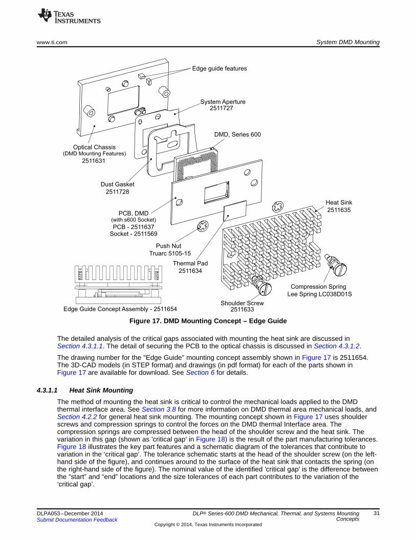
4.3.1 Edge Guide Mounting ConceptThe main characteristics of this mounting concept are discussed in Section 4.2. Additional information andspecific part details are discussed in this section. The design concept for mounting the Series-600 DMDshown in Figure 17 incorporates specific features on the optical chassis intended to aid in the alignment ofthe DMD during the installation of the DMD. The DMD Datum’s (‘A’, ‘B’, and ‘C’) along with theircorresponding features on the optical chassis can be used as the sole alignment features when installingthe DMD, but these features are small, close to the window, and not easily seen during installation ofDMD. The edge alignment features on the optical chassis are intended to simply the assembly processand reduce the chance of damaging the DMD window due to inadvertent contact between the DMDwindow and the alignment pins on the optical chassis (Datum’s ‘B’ and ‘C’). The edge alignment features(shown in Figure 17) are larger and provide rough alignment to the edge of the DMD ceramic carrierbefore the small datum pin features are near the window. The Datum ‘A’, ‘B’, and ‘C’ features (describedin earlier sections) are intended to provide the final alignment.
30 DLP® Series-600 DMD Mechanical, Thermal, and Systems Mounting DLPA053–December 2014Concepts Submit Documentation Feedback
Copyright © 2014, Texas Instruments Incorporated
PCB, DMD
Thermal Pad
(with s600 Socket)
Optical Chassis(DMD Mounting Features)
Dust Gasket
System Aperture
Push Nut
Heat Sink
Compression Spring
Shoulder Screw
DMD, Series 600
2511728
Truarc 5105-15
2511635
Lee Spring LC038D01S
2511633
2511634
PCB - 2511637Socket - 2511569
2511631
2511727
Edge guide features
Edge Guide Concept Assembly - 2511654
www.ti.com System DMD Mounting
Figure 17. DMD Mounting Concept – Edge Guide
The detailed analysis of the critical gaps associated with mounting the heat sink are discussed inSection 4.3.1.1. The detail of securing the PCB to the optical chassis is discussed in Section 4.3.1.2.
The drawing number for the "Edge Guide" mounting concept assembly shown in Figure 17 is 2511654.The 3D-CAD models (in STEP format) and drawings (in pdf format) for each of the parts shown inFigure 17 are available for download. See Section 6 for details.
4.3.1.1 Heat Sink MountingThe method of mounting the heat sink is critical to control the mechanical loads applied to the DMDthermal interface area. See Section 3.8 for more information on DMD thermal area mechanical loads, andSection 4.2.2 for general heat sink mounting. The mounting concept shown in Figure 17 uses shoulderscrews and compression springs to control the forces on the DMD thermal Interface area. Thecompression springs are compressed between the head of the shoulder screw and the heat sink. Thevariation in this gap (shown as 'critical gap' in Figure 18) is the result of the part manufacturing tolerances.Figure 18 illustrates the key part features and a schematic diagram of the tolerances that contribute tovariation in the ‘critical gap’. The tolerance schematic starts at the head of the shoulder screw (on the left-hand side of the figure), and continues around to the surface of the heat sink that contacts the spring (onthe right-hand side of the figure). The nominal value of the identified 'critical gap' is the difference betweenthe “start” and “end” locations and the size tolerances of each part contributes to the variation of the‘critical gap’.
31DLPA053–December 2014 DLP® Series-600 DMD Mechanical, Thermal, and Systems MountingConceptsSubmit Documentation Feedback
Copyright © 2014, Texas Instruments Incorporated

Shoulder Screw
Critical Gap,Spring
Compressive Spring (Coil)
Heat Sink
DMD
Thermal Pad
Boss, OpticalChassis
Start
End
System DMD Mounting www.ti.com
Figure 18. Heat Sink Mounting Tolerance Analysis Schematic Diagram
The nominal value and tolerance for each of the key part features shown in Figure 18 that contribute tothe gap are included in the analysis shown in Table 1. The nominal and tolerance values are found on theindividual part drawings for the mounting concept shown in Figure 17. See Section 6 for drawinginformation. The parts are dimensioned in a manor to minimize variations in the gap.
The tolerance analysis indicates a nominal gap size of 7.1294 mm. The simple sum (SUM) method of parttolerance analysis (worst-case) is ±0.6200 mm, which results in a minimum gap of 6.509 mm, and amaximum of 7.749 mm. The root sum square (RSS) method of part tolerance analysis is ±0.3127 mm,which result in a minimum gap of 6.817 mm and a maximum of 7.442 mm.
Table 1. Gap for Compression Spring
Tol Min MaxNominal (mm) Dir Sign Nominal (mm) Tol (+/-) (mm) Method Gap GapShoulder Screw 15.3900 -1 –15.3900 0.0800
Optical Chassis (Datum 'A' to 5.0000 -1 –5.0000 0.1200Should Screw Boss)DMD 2.9500 1 2.9500 0.2400
Thermal Pad (compressed 0.4826 1 0.4826 0.0500height)Heat SInk 9.8280 1 9.8280 0.1300
0.6200 6.509 7.749Sum –7.1294 (1) Sum RSS0.3127 6.817 7.442(1) Negative indicates a gap for spring
The resultant force on the DMD thermal interface area depends upon:• Minimum and maximum critical gap size for the compression spring (from above analysis)• Nominal free length of the spring• Tolerance of the spring free length• Nominal spring rate• Tolerance of the spring rate
For the concept design illustrated in Figure 17 the minimum force required for thermal performance of thethermal pad is determined as follows:• Area of the heat sink stud and thermal pad is 12.7 × 18.4 = 234 mm2
• To achieve a thermal pad resistance of 0.54°C/Watt will require a pressure of 171 KPa on the thermal
32 DLP® Series-600 DMD Mechanical, Thermal, and Systems Mounting DLPA053–December 2014Concepts Submit Documentation Feedback
Copyright © 2014, Texas Instruments Incorporated

www.ti.com System DMD Mounting
area (pressure from thermal pad data sheet)• To achieve a pressure of 171 KPa on the 234 mm2 thermal area would require a total load of 40
Newton be applied to the DMD Thermal Interface area• Since two compression springs are used the minimum needed per spring is 20 Newton
For a maximum load of 111 Newton applied to the DMD Thermal area the load per spring would be 55.5Newton. Thus, the compression spring to be selected (or designed) for this application should produce aminimum of 20 Newton and a maximum of 55.5 Newton. For the springs reviewed in this force range thetypical spring free length tolerance was ±0.56 mm, and a spring rate tolerance was ±10% of the nominalspring rate.
The nominal force occurs when:• The gap is as designed (no tolerances associated with part manufacturing applied)• The spring rate is the nominal specified value• The free length is the ‘as designed‘ length (no tolerances associated with part manufacturing applied)
The maximum force occurs when:• The gap is the smallest (using either SUM or RSS tolerance analysis)• Spring rate is at the high side of tolerances• Free length of the spring is on the high side of the tolerances
The minimum force occurs when:• The gap is the largest (using either SUM or RSS tolerance analysis)• Spring rate is on the low side of tolerance• Free length of the spring is on the low side of the tolerances
Table 2 summarizes the SUM (worst-case) and RSS tolerance analysis results for several candidatesprings.
Table 2. Analysis Summary for DMD Thermal Area Mechanical Load
DMD Thermal Area Load (force)Outside Solid Free Spring Worst Case RSS CaseWire Rod NominalSpring Dia Length Length Rate Tolerances TolerancesDia (mm) Dia (mm)(mm) (mm) (mm) (N/mm) Min Min(N) Max (N) Max (N)(N) (N)
19.57 43.94 21.71 41.33A 7.619 0.965 5.105 5.460 11.125 7.72 30.85B 7.619 1.016 5.537 5.359 11.125 9.91 39.60 25.12 56.41 27.86 53.06C 8.991 1.092 5.054 6.578 10.998 9.87 38.18 23.89 54.80 26.62 51.46D 9.143 1.066 5.105 6.781 11.125 8.15 32.56 20.66 46.39 22.92 43.63
The results of the tolerance analysis indicates:• All springs (A, B, C, D) have a nominal force that is between the minimum and maximum loads
required (20.0 - 55.5 N).• Spring (A) has a worst-case (SUM) load for minimum tolerances (19.57 N) just under the 20.0 N
minimum, but the RSS load (21.71 N) is greater than the minimum needed.• Spring (B) has a worst-case (SUM) load for the maximum tolerances (56.41 N) over the 55.5 N
maximum, but the RSS load (53.06 N) is less than the maximum requirement• Spring (C) has loads that are between the minimum and maximum loads required although the worst-
case (SUM) load (54.80 N) is just below the maximum requirement• Spring (D) has loads that are between the minimum and maximum loads required although the worst-
case (SUM) load (20.66 N) is just above the minimum required
A final selection between these spring candidates would be based on several factors, including but notlimited to:• What is the likelihood that the worst-case (SUM) conditions would occur?
33DLPA053–December 2014 DLP® Series-600 DMD Mechanical, Thermal, and Systems MountingConceptsSubmit Documentation Feedback
Copyright © 2014, Texas Instruments Incorporated

Mounting Screw
Critical Gap
Optical Chassis PCB, DMD
DMD
Socket, DMD
Boss, OpticalChassis
Start
End
System DMD Mounting www.ti.com
• If the worst-case (SUM) conditions did occur what type of failure is likely to result? (Would the DMD bedamaged, the electrical connection to the DMD be compromised or general damage?)
• If a failure did result, could it be identified before the end-application was shipped to the finalcustomer?
• If a failure did result, what would the impact on the final customer be?
4.3.1.2 PCB MountingIt is recommended that the PCB be mounted using some type of a "direct control" method, like thosedescribed in Section 4.3.1.1. A method based on the ‘Interface Bracket to PCB’ is the simplest. The detailsof the bracket designs are very specific to the geometry of the end-application and will not be covered indetail.
Analysis of the 'critical gap' between the PCB and the boss on the optical interface shown in Figure 19 isnot needed when a direct control mounting method is used, but such an analysis may help to understandthe potential for PCB bending when making a decision on which mounting method to use.
One of the key items to implement the "indirect control" method (if chosen) is to minimize bending of theDMD-PCB. Minimizing the 'critical gap' (shown in Figure 19) between the DMD-PCB and thecorresponding boss on the optical chassis will reduce the potential for bending.
This is achieved by minimizing the gap between the DMD-PCB and the corresponding boss on the opticalchassis (optical interface). The parts in Figure 17 that contribute to the variation in the ‘critical gap’ areshown in Figure 19 along with a tolerance schematic diagram. The tolerance schematic diagram starts atthe top of the mounting screw boss on the optical chassis (in the top left-hand corner of the figure) andcontinues around to the face of the PCB closest to the optical chassis (in the top right-hand corner of thefigure). In the ideal situation the PCB would be infinitely rigid and would not bend due to the force appliedby the screw, but this is not the case. The PCB is likely to bend and the largest ‘critical gap’ sizedetermines the maximum amount of bending that can occur.
Figure 19. DMD-PCB Gap Analysis Schematic Diagram
Table 3 lists the nominal value and tolerance for each feature that contributes to the size of the 'criticalgap'. The nominal values and tolerances used are those on the part drawings for the "Edge Guide"mounting concept shown in Figure 17. The parts are dimensioned in a manor to minimize variations in the“critical gap”. The tolerance analysis indicates the nominal gap size is 0.6500 mm. The simple sum (SUM)method of tolerance analysis (worst-case) yields a tolerance of ±0.5600 mm, which results in a minimumgap of 0.090 mm, and a maximum gap of 1.210 mm. The root sum square (RSS) method of toleranceanalysis yields a tolerance of ±0.3347 mm, which results in a minimum gap of 0.315 mm and a maximumgap of 0.985 mm.
34 DLP® Series-600 DMD Mechanical, Thermal, and Systems Mounting DLPA053–December 2014Concepts Submit Documentation Feedback
Copyright © 2014, Texas Instruments Incorporated

www.ti.com System Sockets
Table 3. Gap between Interface Boss and DMD-PCB
Tol (+/-) Tol Min MaxNominal (mm) Dir Sign Nominal (mm) (mm) Method Gap GapOptical Chassis (Datum 'A' 5.0000 -1 –5.0000 0.1200to PCB Boss
DMD 2.9500 1 2.9500 0.2400Socket, DMD 2.7000 1 2.7000 0.2000
0.5600 Sum 0.090 1.210Sum 0.6500 (1) 0.3347 RSS 0.315 0.985(1) Positive indicates a gap between interface boss and PCBoard
The height of the boss on the optical chassis was designed to result in a minimum gap of nearly zero forthe worst-case tolerances. A minimum gap greater than zero is needed to ensure the DMD Datum ‘A’ andits corresponding feature on the optical chassis are in contact. If the PCB contacts the boss (on the opticalchassis) before the Datum ‘A’ features then focus and focus uniformity could be impacted.
5 System SocketsThe Micro-PGA pins on the Series-600 DMD have the same diameter, length, and spacing as manymicroprocessor chips. This enables the socket contacts developed for the microprocessor chip sockets tobe used for the DMD sockets. The physical arrangement of the contacts on the DMD is different thanthose for any microprocessor; therefore the holder (or housing) that holds (and retains) the contacts isunique to the DMD sockets. But the contact design and process for manufacturing the sockets are oftenthe same.
Low insertion force (LIF) and zero insertion force (ZIF) style of contacts are typically available that willmate with the pins on the DMD. The insertion force on the DMD is thought to be too large for using a LIFstyle contact because of the large number of pins on the Series-600 DMD (350 pins).
Mechanical outline control envelope specifications are available for a zero insertion force (ZIF) stylesocket. The outline specifications define the features, which are necessary for the socket to mechanicallyinterface with a Series-600 DMD. Contact design details are unique and proprietary to each socketmanufacture, and are therefore omitted from the outline specification. Multiple contact designs fromdifferent manufactures will work with the pins on the DMD. Consult the individual socket manufacture forinformation related to specific socket performance characteristics.
The purpose of the outline envelope specification is to provide a standard set of criteria for development ofsockets by different manufacturers. This enables sockets from different manufacturers to beinterchangeable without the need to make any changes to the DMD-PCB, or the mechanical parts used tomount the DMD.
Drawings and 3D-CAD models of the outline envelop specifications are available to DLP® customers andhave also been provided to socket manufactures. The 3D-CAD models (in STEP format) and drawings (inpdf format) of the ZIF style sockets are available for download, see Section 6.
TI has worked with a socket supplier to develop a ZIF style socket. Other sockets supplier are capable tomake a socket as well. TI does not perform socket certification or qualification, nor does TI require socketsuppliers to conduct any specific suite of tests during development of the sockets. TI encourages socketsuppliers to conduct the existing industry standard tests for these type of sockets (as an indication of thereliability of the socket). The final selection of the socket and supplier is the choice of each DLP Customer.It is the responsibility of each customer to verify that a given socket meets the functional and qualityrequirements for their end-application.
5.1 Socket Design and Selection ConsiderationsWhen designing or selecting a socket to be used with the Series-600 DMD the following factors should beconsidered:• Style of Socket – both zero insertion force and low insertion force style contacts have been
successfully demonstrated with DMDs. Each style has its own characteristics to be considered.Generally the LIF style have a smaller foot print on the DMD-PCB and the ZIF are easier to assemble.
35DLPA053–December 2014 DLP® Series-600 DMD Mechanical, Thermal, and Systems MountingConceptsSubmit Documentation Feedback
Copyright © 2014, Texas Instruments Incorporated

System Sockets www.ti.com
• Installed Height - the ‘Installed Height’ shown in Figure 20 represents the distance from the top surfaceof the DMD-PCB to the “DMD-seating plane" on the socket. The "DMD-seating plane" (shown inFigure 20) is the surface of the socket that will make contact with the DMD. Figure 4 illustrates the"socket-seating plane" on the DMD. The socket installed height is one of the key factors whendetermining the amount the DMD-PCB could bend if mounted by clamping against bosses on theoptical chassis (see the "indirect control" method described in Section 4.2.3.2 and Section 4.3.1.2)
Figure 20. Socket Installed Height
• Overall X-Y Dimensions – The overall socket dimensions influence the foot print size needed on thePCB and ultimately the amount of space required for mounting the DMD. ZIF style sockets typicallyhave larger X-Y dimensions than a LIF style socket. Consequently the DMD mounting hardware mustbe located further from the DMD than with LIF style sockets.
• Electrical Contact Resistance - The electrical contact resistance between the DMD pin and the socketcontact should be minimal. A contact resistance of 30 milliohms is a good reasonable objective andshould easily be achieved with contact designs available from socket suppliers.
• Contact Insertion Force – the contact insertion force is the force that must be applied to each socketcontact by the DMD pin in order to fully seat the pin into a contact (for example, for the DMD-seatingplane to make complete contact with the socket-seating plane). The contact insertion force multipliedby the total number of pins is the resultant forces that must be applied to the DMD in order to fully seatthe DMD. The higher the contact insertion force, the more likely that the socket or DMD could becomedamaged during assembly. As the name implies the ZIF style sockets do not require any insertionforce. The total force required to insert the DMD into the socket should not exceed the DMDmechanical loads described in Section 3.8.
• Contact extraction force – the contact extraction force is the force required to overcome the retentionforces of the contacts during removal of the DMD from the socket. A socket with a high extraction forceis susceptible to damage of the contact solder joint (on the PCB pad), the socket contacts, DMD pins,or DMD ceramic carrier if the DMD is not uniformly removed from the socket (all pins removed at thesame time). ZIF style sockets have no extraction force.
• When using a non-ZIF style socket (LIF), it is recommended that an extraction tool or aid be designedand used to ease removal of the DMD and reduce the possibility of damage to the socket or DMD.Typically an extraction tool will make contact-with and press against the PCB. Areas on the PCBshould be defined and identified as "allowable contact areas". These areas should be kept free of bothcomponents and surface traces in order to prevent damage from the extraction tool.
• Coefficient of thermal expansion (CTE) – typically the socket and PCB will be made of distinctlydifferent materials and thus different CTE values. DMD sockets are larger than typical componentssoldered to a PCB. Because of the physical size and materials used, a “significant” CTE mismatch ispossible between the socket and the PCB, which can result in solder joint failures during periods ofhigh temperature cycling. What is considered a “significant” CTE mismatch will depend upon thetemperature extremes over which the end-application will operate, but more importantly the solderprofile used to attach the socket to the PCB. Strict adherence to the solder profiles recommended bythe socket suppliers is recommended. Not using the recommended solder profile can result in higherthan expected contact insertion and extraction forces.
• Pick and place features - features that facilitate vacuum pickup, and placement of the socket onto thePCB prior to solder. Some socket suppliers supply a molded cap which is clipped over the contacthousing while other suppliers place a piece of kapton (polyimide) tape over the contacts and centeropening.
36 DLP® Series-600 DMD Mechanical, Thermal, and Systems Mounting DLPA053–December 2014Concepts Submit Documentation Feedback
Copyright © 2014, Texas Instruments Incorporated

Note: DMD-Pin is not concentric with PCB-Pad
www.ti.com System Sockets
5.2 Series-600 SocketA zero insertion force (ZIF) style socket has been developed and is available for use with the Series-600DMDs. The socket is commonly referred to as the Series-600 socket and has 350 contacts.
The key characteristics and considerations of the socket are illustrated in Figure 21 and include:• Overall dimensions• Opening to accommodate a heat sink stud used to cool the DMD• Installed height of 2.700 mm; Important for some methods of mounting the DMD-PCB for control of
loads applied to the DMD electrical interface area• Offset between DMD pin and PCB pad of 0.3875 mm• No force applied to the DMD when inserting or removing the DMD from the socket• Tools to aid insertion or extraction of the DMD from the socket are not likely needed
The TI drawing number for the ZIF style socket design is 2511569. A 3D-CAD file of the socket nominalgeometry (in STEP format) and drawing (in pdf format) are available for download, see Section 6.
Figure 21. Zero Insertion Force Style Series-600 Socket
37DLPA053–December 2014 DLP® Series-600 DMD Mechanical, Thermal, and Systems MountingConceptsSubmit Documentation Feedback
Copyright © 2014, Texas Instruments Incorporated

Drawing and 3D-CAD File References www.ti.com
6 Drawing and 3D-CAD File ReferencesDrawings (in pdf format) and 3D-CAD models (in STEP format) for many of the parts discussed in thisapplication report are available to facilitate study, when designing an end-application. Table 4 summarizesthe literature numbers for the drawings and 3D-CAD models that are available for download from the linksin the table.
Table 4. Reference Drawings and 3D-CAD Models
LITERATURE NUMBER DESCRIPTIONDLPS053 DLP6500FYE DMD (.65 1080 Series-600) Data SheetDLPR006 DLP6500FYE DMD (.65 1080 Series-600) 3D-CAD model file with nominal geometry
Assembly and part drawings of Edge Guide Mounting Concept (2511654) – also includes 3D-DLPC091 CAD model filesDLPC092 Series-600 ZIF style socket (2511569) part drawing - also includes 3D-CAD model files
38 DLP® Series-600 DMD Mechanical, Thermal, and Systems Mounting DLPA053–December 2014Concepts Submit Documentation Feedback
Copyright © 2014, Texas Instruments Incorporated

IMPORTANT NOTICE
Texas Instruments Incorporated and its subsidiaries (TI) reserve the right to make corrections, enhancements, improvements and otherchanges to its semiconductor products and services per JESD46, latest issue, and to discontinue any product or service per JESD48, latestissue. Buyers should obtain the latest relevant information before placing orders and should verify that such information is current andcomplete. All semiconductor products (also referred to herein as “components”) are sold subject to TI’s terms and conditions of salesupplied at the time of order acknowledgment.TI warrants performance of its components to the specifications applicable at the time of sale, in accordance with the warranty in TI’s termsand conditions of sale of semiconductor products. Testing and other quality control techniques are used to the extent TI deems necessaryto support this warranty. Except where mandated by applicable law, testing of all parameters of each component is not necessarilyperformed.TI assumes no liability for applications assistance or the design of Buyers’ products. Buyers are responsible for their products andapplications using TI components. To minimize the risks associated with Buyers’ products and applications, Buyers should provideadequate design and operating safeguards.TI does not warrant or represent that any license, either express or implied, is granted under any patent right, copyright, mask work right, orother intellectual property right relating to any combination, machine, or process in which TI components or services are used. Informationpublished by TI regarding third-party products or services does not constitute a license to use such products or services or a warranty orendorsement thereof. Use of such information may require a license from a third party under the patents or other intellectual property of thethird party, or a license from TI under the patents or other intellectual property of TI.Reproduction of significant portions of TI information in TI data books or data sheets is permissible only if reproduction is without alterationand is accompanied by all associated warranties, conditions, limitations, and notices. TI is not responsible or liable for such altereddocumentation. Information of third parties may be subject to additional restrictions.Resale of TI components or services with statements different from or beyond the parameters stated by TI for that component or servicevoids all express and any implied warranties for the associated TI component or service and is an unfair and deceptive business practice.TI is not responsible or liable for any such statements.Buyer acknowledges and agrees that it is solely responsible for compliance with all legal, regulatory and safety-related requirementsconcerning its products, and any use of TI components in its applications, notwithstanding any applications-related information or supportthat may be provided by TI. Buyer represents and agrees that it has all the necessary expertise to create and implement safeguards whichanticipate dangerous consequences of failures, monitor failures and their consequences, lessen the likelihood of failures that might causeharm and take appropriate remedial actions. Buyer will fully indemnify TI and its representatives against any damages arising out of the useof any TI components in safety-critical applications.In some cases, TI components may be promoted specifically to facilitate safety-related applications. With such components, TI’s goal is tohelp enable customers to design and create their own end-product solutions that meet applicable functional safety standards andrequirements. Nonetheless, such components are subject to these terms.No TI components are authorized for use in FDA Class III (or similar life-critical medical equipment) unless authorized officers of the partieshave executed a special agreement specifically governing such use.Only those TI components which TI has specifically designated as military grade or “enhanced plastic” are designed and intended for use inmilitary/aerospace applications or environments. Buyer acknowledges and agrees that any military or aerospace use of TI componentswhich have not been so designated is solely at the Buyer's risk, and that Buyer is solely responsible for compliance with all legal andregulatory requirements in connection with such use.TI has specifically designated certain components as meeting ISO/TS16949 requirements, mainly for automotive use. In any case of use ofnon-designated products, TI will not be responsible for any failure to meet ISO/TS16949.
Products ApplicationsAudio www.ti.com/audio Automotive and Transportation www.ti.com/automotiveAmplifiers amplifier.ti.com Communications and Telecom www.ti.com/communicationsData Converters dataconverter.ti.com Computers and Peripherals www.ti.com/computersDLP® Products www.dlp.com Consumer Electronics www.ti.com/consumer-appsDSP dsp.ti.com Energy and Lighting www.ti.com/energyClocks and Timers www.ti.com/clocks Industrial www.ti.com/industrialInterface interface.ti.com Medical www.ti.com/medicalLogic logic.ti.com Security www.ti.com/securityPower Mgmt power.ti.com Space, Avionics and Defense www.ti.com/space-avionics-defenseMicrocontrollers microcontroller.ti.com Video and Imaging www.ti.com/videoRFID www.ti-rfid.comOMAP Applications Processors www.ti.com/omap TI E2E Community e2e.ti.comWireless Connectivity www.ti.com/wirelessconnectivity
Mailing Address: Texas Instruments, Post Office Box 655303, Dallas, Texas 75265Copyright © 2014, Texas Instruments Incorporated