
DLP4501 (0.45 WXGA S311 DMD) - Analog, Embedded … · DLP4501 (0.45 WXGA S311 DMD) 1 Features 3...
39
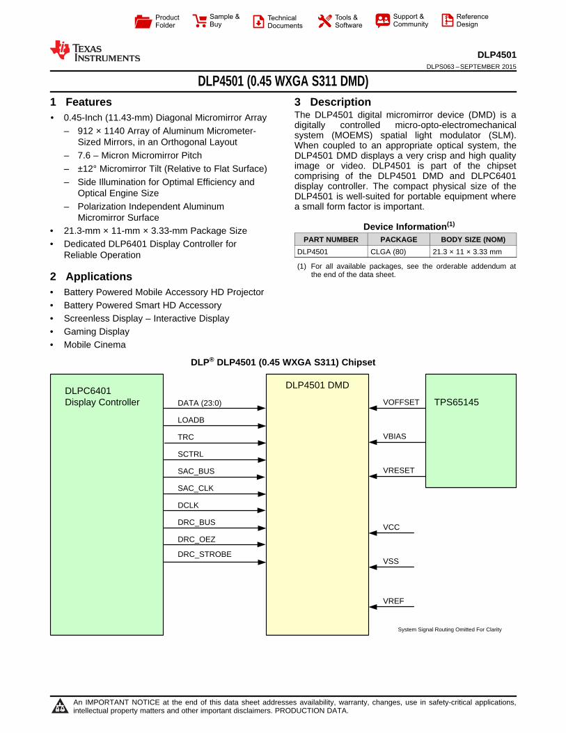
DLPC6401 Display Controller DLP4501 DMD TPS65145 VOFFSET VBIAS VRESET DATA (23:0) LOADB TRC SCTRL SAC_BUS SAC_CLK DCLK DRC_BUS DRC_OEZ DRC_STROBE VCC VSS VREF System Signal Routing Omitted For Clarity Product Folder Sample & Buy Technical Documents Tools & Software Support & Community Reference Design DLP4501 DLPS063 – SEPTEMBER 2015 DLP4501 (0.45 WXGA S311 DMD) 1 Features 3 Description The DLP4501 digital micromirror device (DMD) is a 1• 0.45-Inch (11.43-mm) Diagonal Micromirror Array digitally controlled micro-opto-electromechanical – 912 × 1140 Array of Aluminum Micrometer- system (MOEMS) spatial light modulator (SLM). Sized Mirrors, in an Orthogonal Layout When coupled to an appropriate optical system, the – 7.6 – Micron Micromirror Pitch DLP4501 DMD displays a very crisp and high quality image or video. DLP4501 is part of the chipset – ±12° Micromirror Tilt (Relative to Flat Surface) comprising of the DLP4501 DMD and DLPC6401 – Side Illumination for Optimal Efficiency and display controller. The compact physical size of the Optical Engine Size DLP4501 is well-suited for portable equipment where – Polarization Independent Aluminum a small form factor is important. Micromirror Surface Device Information (1) • 21.3-mm × 11-mm × 3.33-mm Package Size PART NUMBER PACKAGE BODY SIZE (NOM) • Dedicated DLP6401 Display Controller for DLP4501 CLGA (80) 21.3 × 11 × 3.33 mm Reliable Operation (1) For all available packages, see the orderable addendum at the end of the data sheet. 2 Applications • Battery Powered Mobile Accessory HD Projector • Battery Powered Smart HD Accessory • Screenless Display – Interactive Display • Gaming Display • Mobile Cinema DLP ® DLP4501 (0.45 WXGA S311) Chipset 1 An IMPORTANT NOTICE at the end of this data sheet addresses availability, warranty, changes, use in safety-critical applications, intellectual property matters and other important disclaimers. PRODUCTION DATA.
Transcript of DLP4501 (0.45 WXGA S311 DMD) - Analog, Embedded … · DLP4501 (0.45 WXGA S311 DMD) 1 Features 3...
DLPC6401Display Controller
DLP4501 DMD
TPS65145VOFFSET
VBIAS
VRESET
DATA (23:0)
LOADB
TRC
SCTRL
SAC_BUS
SAC_CLK
DCLK
DRC_BUS
DRC_OEZ
DRC_STROBE
VCC
VSS
VREF
System Signal Routing Omitted For Clarity
Product
Folder
Sample &Buy
Technical
Documents
Tools &
Software
Support &Community
ReferenceDesign
DLP4501DLPS063 –SEPTEMBER 2015
DLP4501 (0.45 WXGA S311 DMD)1 Features 3 Description
The DLP4501 digital micromirror device (DMD) is a1• 0.45-Inch (11.43-mm) Diagonal Micromirror Array
digitally controlled micro-opto-electromechanical– 912 × 1140 Array of Aluminum Micrometer- system (MOEMS) spatial light modulator (SLM).Sized Mirrors, in an Orthogonal Layout When coupled to an appropriate optical system, the
– 7.6 – Micron Micromirror Pitch DLP4501 DMD displays a very crisp and high qualityimage or video. DLP4501 is part of the chipset– ±12° Micromirror Tilt (Relative to Flat Surface)comprising of the DLP4501 DMD and DLPC6401– Side Illumination for Optimal Efficiency and display controller. The compact physical size of the
Optical Engine Size DLP4501 is well-suited for portable equipment where– Polarization Independent Aluminum a small form factor is important.
Micromirror SurfaceDevice Information(1)
• 21.3-mm × 11-mm × 3.33-mm Package SizePART NUMBER PACKAGE BODY SIZE (NOM)• Dedicated DLP6401 Display Controller for
DLP4501 CLGA (80) 21.3 × 11 × 3.33 mmReliable Operation(1) For all available packages, see the orderable addendum at
the end of the data sheet.2 Applications• Battery Powered Mobile Accessory HD Projector• Battery Powered Smart HD Accessory• Screenless Display – Interactive Display• Gaming Display• Mobile Cinema
DLP® DLP4501 (0.45 WXGA S311) Chipset
1
An IMPORTANT NOTICE at the end of this data sheet addresses availability, warranty, changes, use in safety-critical applications,intellectual property matters and other important disclaimers. PRODUCTION DATA.
DLP4501DLPS063 –SEPTEMBER 2015 www.ti.com
Table of Contents7.4 Device Functional Modes........................................ 201 Features .................................................................. 17.5 Window Characteristics and Optics ........................ 202 Applications ........................................................... 17.6 Micromirror Array Temperature Calculation............ 213 Description ............................................................. 17.7 Micromirror Landed-On/Landed-Off Duty Cycle .... 224 Revision History..................................................... 2
8 Application and Implementation ........................ 255 Pin Configuration and Functions ......................... 38.1 Application Information............................................ 256 Specifications......................................................... 78.2 Typical Application .................................................. 256.1 Absolute Maximum Ratings ...................................... 7
9 Power Supply Recommendations ...................... 286.2 Storage Conditions.................................................... 79.1 Power Supply Power-Up Procedure ...................... 286.3 ESD Ratings.............................................................. 89.2 Power Supply Power-Down Procedure .................. 286.4 Recommended Operating Conditions ...................... 89.3 Power Supply Sequencing Requirements .............. 296.5 Thermal Information ................................................ 10
10 Layout................................................................... 316.6 Electrical Characteristics......................................... 1010.1 Layout Guidelines ................................................. 316.7 Timing Requirements .............................................. 1210.2 Layout Example .................................................... 316.8 System Mounting Interface Loads .......................... 15
11 Device and Documentation Support ................. 326.9 Physical Characteristics of the Micromirror Array... 1611.1 Device Support...................................................... 326.10 Micromirror Array Optical Characteristics ............ 1711.2 Related Links ........................................................ 326.11 Window Characteristics......................................... 1811.3 Community Resources.......................................... 336.12 Chipset Component Usage Specification ............. 1811.4 Trademarks ........................................................... 337 Detailed Description ............................................ 1911.5 Electrostatic Discharge Caution............................ 337.1 Overview ................................................................. 1911.6 Glossary ................................................................ 337.2 Functional Block Diagram ....................................... 19
12 Mechanical, Packaging, and Orderable7.3 Feature Description................................................. 20Information ........................................................... 33
4 Revision History
DATE REVISION NOTESSeptember 2015 * Initial release.
2 Submit Documentation Feedback Copyright © 2015, Texas Instruments Incorporated
Product Folder Links: DLP4501
DLP4501www.ti.com DLPS063 –SEPTEMBER 2015
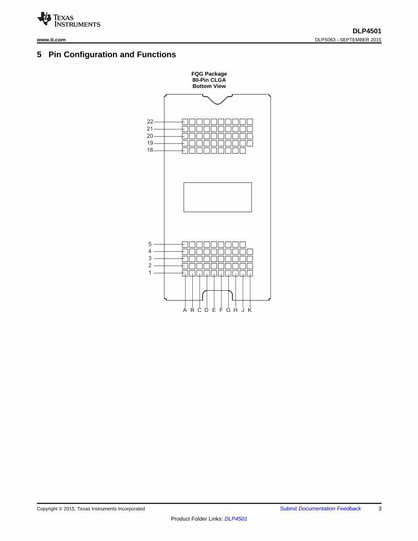
5 Pin Configuration and Functions
FQG Package80-Pin CLGABottom View
Copyright © 2015, Texas Instruments Incorporated Submit Documentation Feedback 3
Product Folder Links: DLP4501

DLP4501DLPS063 –SEPTEMBER 2015 www.ti.com
Pin Functions – Connector PinsPIN CLOCKED DATATYPE SIGNAL DESCRIPTIONBY RATENAME NO.
DATA INPUTSDATA(0) A1 I LVCMOS DCLK DDRDATA(1) A2 I LVCMOS DCLK DDRDATA(2) A3 I LVCMOS DCLK DDRDATA(3) A4 I LVCMOS DCLK DDRDATA(4) B1 I LVCMOS DCLK DDRDATA(5) B3 I LVCMOS DCLK DDRDATA(6) C1 I LVCMOS DCLK DDRDATA(7) C3 I LVCMOS DCLK DDRDATA(8) C4 I LVCMOS DCLK DDRDATA(9) D1 I LVCMOS DCLK DDRDATA(10) D4 I LVCMOS DCLK DDRDATA(11) E1 I LVCMOS DCLK DDR
Input data busDATA(12) E4 I LVCMOS DCLK DDRDATA(13) F1 I LVCMOS DCLK DDRDATA(14) F3 I LVCMOS DCLK DDRDATA(15) G1 I LVCMOS DCLK DDRDATA(16) G2 I LVCMOS DCLK DDRDATA(17) G4 I LVCMOS DCLK DDRDATA(18) H1 I LVCMOS DCLK DDRDATA(19) H2 I LVCMOS DCLK DDRDATA(20) H4 I LVCMOS DCLK DDRDATA(21) J1 I LVCMOS DCLK DDRDATA(22) J3 I LVCMOS DCLK DDRDATA(23) J4 I LVCMOS DCLK DDRDCLK K1 I LVCMOS - - Input data bus clockCONTROL INPUTSLOADB K2 I LVCMOS DCLK DDR Parallel data load enableTRC K4 I LVCMOS DCLK DDR Input data toggle rate controlSCTRL K3 I LVCMOS DCLK DDR Serial control busSAC_BUS C20 I LVCMOS SAC_CLK - Stepped address control serial dataSAC_CLK C22 I LVCMOS - - Stepped address control serial clockMIRROR RESET CONTROL INPUTSDRC_BUS B21 I LVCMOS SAC_CLK DMD reset-control serial busDRC_OEZ A20 I LVCMOS - - Active-low output enable signal for internal DMD Reset
driver circuitryDRC_STROBE A22 I LVCMOS SAC_CLK Strobe signal for DMD Reset Control inputsPOWER
C19,VBIAS (1) Power Analog Mirror Reset Bias VoltageD19A19,VOFFSET (1) Power Analog Mirror Reset Offset VoltageK19E19,VRESET (1) Power Analog Mirror Reset VoltageF19B19, Power Supply for Low Voltage CMOS Double-Data-VREF (1) Power AnalogJ19 Rate (DDR) Interface
(1) The following power supplies are all required to operate the DMD: VSS, VCC, VREF, VOFFSET, VBIAS, VRESET.
4 Submit Documentation Feedback Copyright © 2015, Texas Instruments Incorporated
Product Folder Links: DLP4501
DLP4501www.ti.com DLPS063 –SEPTEMBER 2015
Pin Functions – Connector Pins (continued)PIN CLOCKED DATATYPE SIGNAL DESCRIPTIONBY RATENAME NO.
B22,C2,D21,E2,E20,E22,F21,G3,VCC (1) Power Analog Power Supply for LVCMOS LogicG19,
G20,G22,H19,H21,J20,J22,K21A21,
B2, B4,B20,C21,
D2, D3,D20,D22,E3,E21,VSS (1) GND Analog Ground - Common return for all power inputsF2, F4,F20,F22,G21,H3,H20,H22,
J2, J21,K20
Copyright © 2015, Texas Instruments Incorporated Submit Documentation Feedback 5
Product Folder Links: DLP4501
DLP4501DLPS063 –SEPTEMBER 2015 www.ti.com
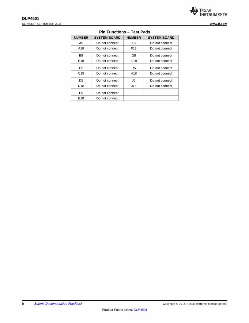
Pin Functions – Test PadsNUMBER SYSTEM BOARD NUMBER SYSTEM BOARD
A5 Do not connect F5 Do not connectA18 Do not connect F18 Do not connect
B5 Do not connect G5 Do not connectB18 Do not connect G18 Do not connect
C5 Do not connect H5 Do not connectC18 Do not connect H18 Do not connect
D5 Do not connect J5 Do not connectD18 Do not connect J18 Do not connect
E5 Do not connectE18 Do not connect
6 Submit Documentation Feedback Copyright © 2015, Texas Instruments Incorporated
Product Folder Links: DLP4501
DLP4501www.ti.com DLPS063 –SEPTEMBER 2015
6 Specifications
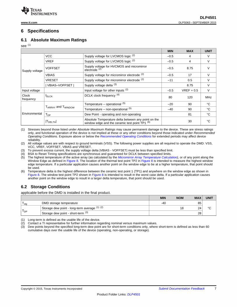
6.1 Absolute Maximum Ratingssee (1)
MIN MAX UNITVCC Supply voltage for LVCMOS logic (2) –0.5 4 VVREF Supply voltage for LVCMOS logic (2) –0.5 4 V
Supply voltage for HVCMOS and micromirrorVOFFSET –0.5 8.75 Velectrode (2)Supply voltageVBIAS Supply voltage for micromirror electrode (2) –0.5 17 VVRESET Supply voltage for micromirror electrode (2) –11 0.5 V| VBIAS–VOFFSET | Supply voltage delta (3) 8.75 V
Input voltage Input voltage for other inputs (2) –0.5 VREF + 0.5 VClock fDLCK DCLK clock frequency (4)
80 120 MHzfrequencyTemperature – operational (5) –20 90 °C
TARRAY and TWINDOW Temperature – non-operational (5) –40 90 °CEnvironmental TDP Dew Point - operating and non-operating 81 °C
Absolute Temperature delta between any point on the|TDELTA| 30 °Cwindow edge and the ceramic test point TP1 (6)
(1) Stresses beyond those listed under Absolute Maximum Ratings may cause permanent damage to the device. These are stress ratingsonly, and functional operation of the device is not implied at these or any other conditions beyond those indicated under RecommendedOperating Conditions. Exposure above or below the Recommended Operating Conditions for extended periods may affect devicereliability.
(2) All voltage values are with respect to ground terminals (VSS). The following power supplies are all required to operate the DMD: VSS,VCC, VREF, VOFFSET, VBIAS and VRESET.
(3) To prevent excess current, the supply voltage delta |VBIAS - VOFFSET| must be less than specified limit.(4) BSA to Reset Timing specifications are synchronous and guaranteed for DCLK between specified limits.(5) The highest temperature of the active array (as calculated by the Micromirror Array Temperature Calculation), or of any point along the
Window Edge as defined in Figure 8. The location of the thermal test point TP2 in Figure 8 is intended to measure the highest windowedge temperature. If a particular application causes another point on the window edge to be at a higher temperature, that point shouldbe used.
(6) Temperature delta is the highest difference between the ceramic test point 1 (TP1) and anywhere on the window edge as shown inFigure 8. The window test point TP2 shown in Figure 8 is intended to result in the worst case delta. If a particular application causesanother point on the window edge to result in a larger delta temperature, that point should be used.
6.2 Storage Conditionsapplicable before the DMD is installed in the final product.
MIN NOM MAX UNITTstg DMD storage temperature -40 85
Storage dew point - long-term average (1) (2) 18 24 °CTDP Storage dew point - short-term (3) 28
(1) Long-term is defined as the usable life of the device.(2) Contact a TI representative for further information regarding nominal versus maximum values.(3) Dew points beyond the specified long-term dew point are for short-term conditions only, where short-term is defined as less than 60
cumulative days over the usable life of the device (operating, non-operating, or storage).
Copyright © 2015, Texas Instruments Incorporated Submit Documentation Feedback 7
Product Folder Links: DLP4501
DLP4501DLPS063 –SEPTEMBER 2015 www.ti.com
6.3 ESD RatingsVALUE UNIT
Electrostatic Human body model (HBM), per ANSI/ESDA/JEDEC JS-001 (1)V(ESD) ±2000 Vdischarge
(1) JEDEC document JEP155 states that 500-V HBM allows safe manufacturing with a standard ESD control process.
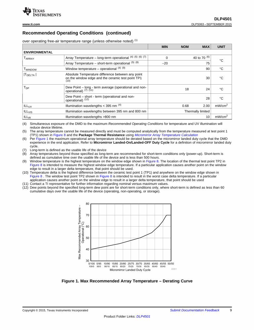
6.4 Recommended Operating Conditionsover operating free-air temperature range (unless otherwise noted) (1)
MIN NOM MAX UNITSUPPLY VOLTAGE RANGE (2)
VREF Supply voltage for LVCMOS interface (3) 1.6 1.8 2.0 VVCC Supply voltage for LVCMOS logic (3) 2.375 2.5 2.625 VVOFFSET Supply voltage for HVCMOS and micromirror 8.25 8.5 8.75 Velectrode (3)
VBIAS Supply voltage for micromirror electrode (3) 15.5 16 16.5 VVRESET Supply voltage for micromirror electrode (3) –9.5 –10 –10.5 V|VBIAS–VOFFSET| Supply voltage delta (absolute value) 8.75 VVp Positive-going threshold voltage 0.4*VREF 0.7*VREF VVn Negative-going threshold voltage 0.3*VREF 0.6*VREF VVh Hysteresis voltage (Vp - Vn) 0.1*VREF 0.4*VREF VVih(DC) DC High level input voltage 0.7*VREF VREF+0.5 VVil(DC) DC Low level input voltage -0.3 0.3*VREF VVih(AC) AC High level input voltage 0.8*VREF VREF+0.5 VVil(AC) AC Low level input voltage -0.3 0.2*VREF V
(1) The functional performance of the device specified in this datasheet is achieved when operating the device within the limits defined bythe Recommended Operating Conditions. No level of performance is implied when operating the device above or below theRecommended Operating Conditions limits.
(2) All voltage values are with respect to the ground pins (VSS).(3) The following power supplies are all required to operate the DMD: VCC, VREF, VOFFSET, VBIAS and VRESET.
8 Submit Documentation Feedback Copyright © 2015, Texas Instruments Incorporated
Product Folder Links: DLP4501
Micromirror Landed Duty Cycle
Ope
ration
al (°
C)
0/100 5/95 10/90 15/85 20/80 25/75 30/70 35/65 40/60 45/5530
40
50
60
70
80
D001
50/50100/0 95/5 90/10 85/15 80/20 75/25 70/30 65/35 60/40 55/45
Max R
ecom
me
nd
ed
Arr
ay
Tem
pe
ratu
re–
DLP4501www.ti.com DLPS063 –SEPTEMBER 2015
Recommended Operating Conditions (continued)over operating free-air temperature range (unless otherwise noted) (1)
MIN NOM MAX UNITENVIRONMENTALTARRAY Array Temperature – long-term operational (4) (5) (6) (7) 0 40 to 70 (6)
°CArray Temperature – short-term operational (5) (8) –20 75
TWINDOW Window temperature – operational (4) (9) 90 °C|TDELTA | Absolute Temperature difference between any point
on the window edge and the ceramic test point TP1 30 °C(10)
TDP Dew Point – long - term average (operational and non- 18 24 °Coperational) (7) (11)
Dew Point – short - term (operational and non- 28 °Coperational) (12)
ILLUV Illumination wavelengths < 395 nm (4) 0.68 2.00 mW/cm2
ILLVIS Illumination wavelengths between 395 nm and 800 nm Thermally limitedILLIR Illumination wavelengths >800 nm 10 mW/cm2
(4) Simultaneous exposure of the DMD to the maximum Recommended Operating Conditions for temperature and UV illumination willreduce device lifetime.
(5) The array temperature cannot be measured directly and must be computed analytically from the temperature measured at test point 1(TP1) shown in Figure 8 and the Package Thermal Resistance using Micromirror Array Temperature Calculation
(6) Per Figure 1 the maximum operational array temperature should be derated based on the micromirror landed duty cycle that the DMDexperience in the end application. Refer to Micromirror Landed-On/Landed-OFF Duty Cycle for a definition of micromirror landed dutycycle.
(7) Long-term is defined as the usable life of the device(8) Array temperatures beyond those specified as long-term are recommended for short-term conditions only (power-up). Short-term is
defined as cumulative time over the usable life of the device and is less than 500 hours.(9) Window temperature is the highest temperature on the window edge shown in Figure 8. The location of the thermal test point TP2 in
Figure 8 is intended to measure the highest window edge temperature. If a particular application causes another point on the windowedge to result in a larger delta temperature, that point should be used.
(10) Temperature delta is the highest difference between the ceramic test point 1 (TP1) and anywhere on the window edge shown inFigure 8 . The window test point TP2 shown in Figure 8 is intended to result in the worst case delta temperature. If a particularapplication causes another point on the window edge to result in a larger delta temperature, that point should be used
(11) Contact a TI representative for further information regarding nominal versus maximum values.(12) Dew points beyond the specified long-term dew point are for short-term conditions only, where short-term is defined as less than 60
cumulative days over the usable life of the device (operating, non-operating, or storage).
SPACE
Figure 1. Max Recommended Array Temperature – Derating Curve
Copyright © 2015, Texas Instruments Incorporated Submit Documentation Feedback 9
Product Folder Links: DLP4501
DLP4501DLPS063 –SEPTEMBER 2015 www.ti.com
6.5 Thermal InformationDLP4501
THERMAL METRIC (1) FQG UNITMIN TYP MAX
Thermal resistance Active area to test point 1 (TP1) 2.00 °C/W
(1) The DMD is designed to conduct absorbed and dissipated heat to the back of the package. The cooling system must be capable ofmaintaining the package within the temperature range specified in the Recommended Operating Conditions . The total heat load onthe DMD is largely driven by the incident light absorbed by the active area; although other contributions include light energy absorbed bythe window aperture and electrical power dissipation of the array. Optical systems should be designed to minimize the light energyfalling outside the window clear aperture since any additional thermal load in this area can significantly degrade the reliability of thedevice.
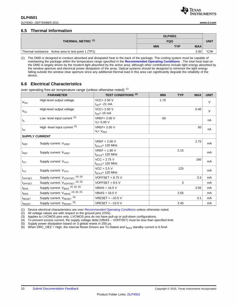
6.6 Electrical Characteristicsover operating free-air temperature range (unless otherwise noted) (1)
PARAMETER TEST CONDITIONS (2) MIN TYP MAX UNITHigh-level output voltage VCC= 2.50 V 1.70VOH VIOH= -21 mAHigh-level output voltage VCC= 2.50 V 0.40VOL VIOH= 15 mALow -level input current (3) VREF= 2.00 V -50IIL nAVI= 0.00 VHigh -level input current (3) VREF= 2.00 V 50IIH nAVI= VREF
SUPPLY CURRENTVREF = 2.00 V 2.75IREF Supply current: VVREF mAfDCLK= 120 MHzVREF = 1.80 V 2.15IREF Supply current: VVREF mAfDCLK= 120 MHzVCC = 2.75 V 160ICC Supply current: VVCC mAfDCLK= 120 MHzVCC = 2.5 V 125ICC Supply current: VVCC mAfDCLK= 120 MHz
IOFFSET Supply current: VVOFFSET(4) (5) VOFFSET = 8.75 V 3.3 mA
IOFFSET Supply current: VVOFFSET(4) (5) VOFFSET = 8.5 V 3 mA
IBIAS Supply current: VBIAS(4) (6) (5) VBIAS = 16.5 V 3.55 mA
IBIAS Supply current: VVBIAS(4) (6) (5) VBIAS = 16.0 V 2.55 mA
IRESET Supply current: VRESET(5) VRESET = –10.5 V 3.1 mA
IRESET Supply current: VRESET(5) VRESET = –10.0 V 2.45 mA
(1) Device electrical characteristics are over Recommended Operating Conditions unless otherwise noted.(2) All voltage values are with respect to the ground pins (VSS).(3) Applies to LVCMOS pins only. LVCMOS pins do not have pull-up or pull-down configurations.(4) To prevent excess current, the supply voltage delta |VBIAS – VOFFSET| must be less than specified limit.(5) Supply power dissipation based on 3 global resets in 200 µs.(6) When DRC_OEZ = High, the internal Reset Drivers are Tri-Stated and IBIAS standby current is 6.5mA
10 Submit Documentation Feedback Copyright © 2015, Texas Instruments Incorporated
Product Folder Links: DLP4501
DLP4501www.ti.com DLPS063 –SEPTEMBER 2015
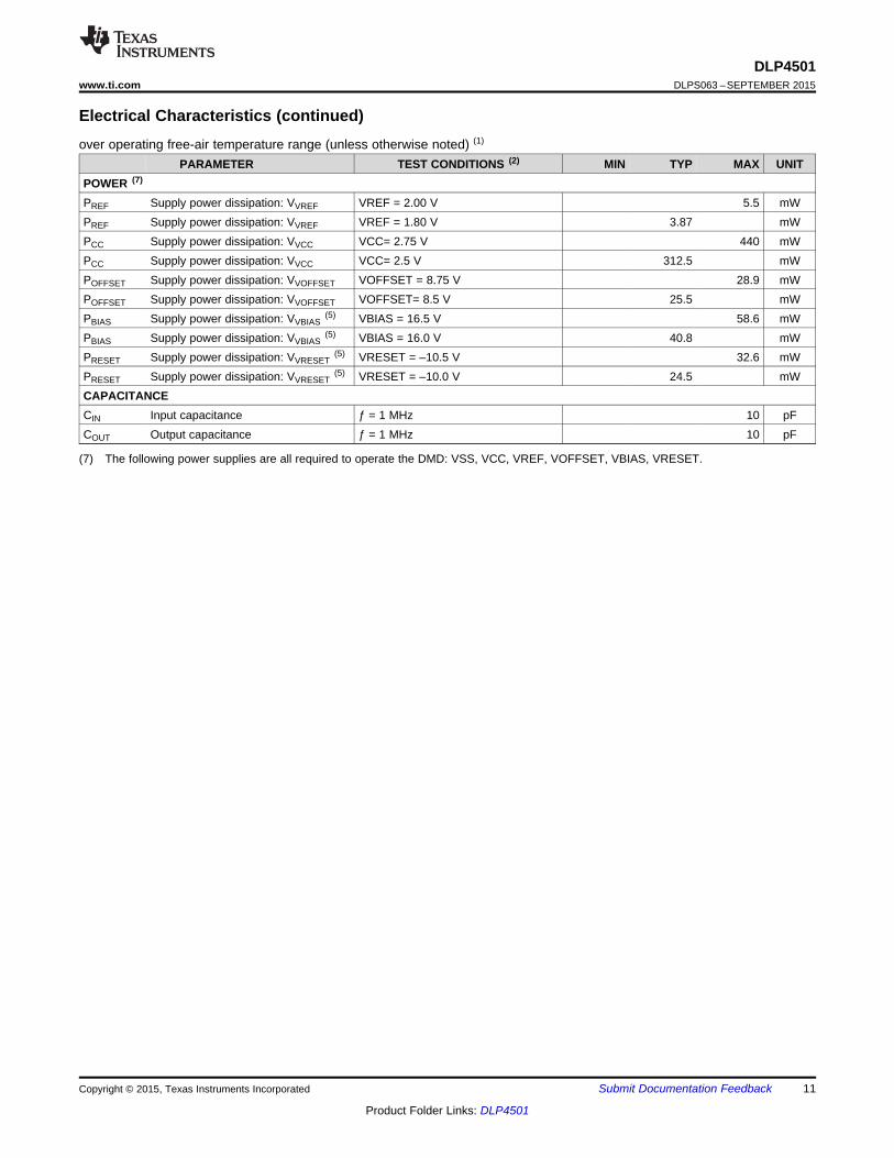
Electrical Characteristics (continued)over operating free-air temperature range (unless otherwise noted) (1)
PARAMETER TEST CONDITIONS (2) MIN TYP MAX UNITPOWER (7)
PREF Supply power dissipation: VVREF VREF = 2.00 V 5.5 mWPREF Supply power dissipation: VVREF VREF = 1.80 V 3.87 mWPCC Supply power dissipation: VVCC VCC= 2.75 V 440 mWPCC Supply power dissipation: VVCC VCC= 2.5 V 312.5 mWPOFFSET Supply power dissipation: VVOFFSET VOFFSET = 8.75 V 28.9 mWPOFFSET Supply power dissipation: VVOFFSET VOFFSET= 8.5 V 25.5 mWPBIAS Supply power dissipation: VVBIAS
(5) VBIAS = 16.5 V 58.6 mWPBIAS Supply power dissipation: VVBIAS
(5) VBIAS = 16.0 V 40.8 mWPRESET Supply power dissipation: VVRESET
(5) VRESET = –10.5 V 32.6 mWPRESET Supply power dissipation: VVRESET
(5) VRESET = –10.0 V 24.5 mWCAPACITANCECIN Input capacitance ƒ = 1 MHz 10 pFCOUT Output capacitance ƒ = 1 MHz 10 pF
(7) The following power supplies are all required to operate the DMD: VSS, VCC, VREF, VOFFSET, VBIAS, VRESET.
Copyright © 2015, Texas Instruments Incorporated Submit Documentation Feedback 11
Product Folder Links: DLP4501
DLP4501DLPS063 –SEPTEMBER 2015 www.ti.com
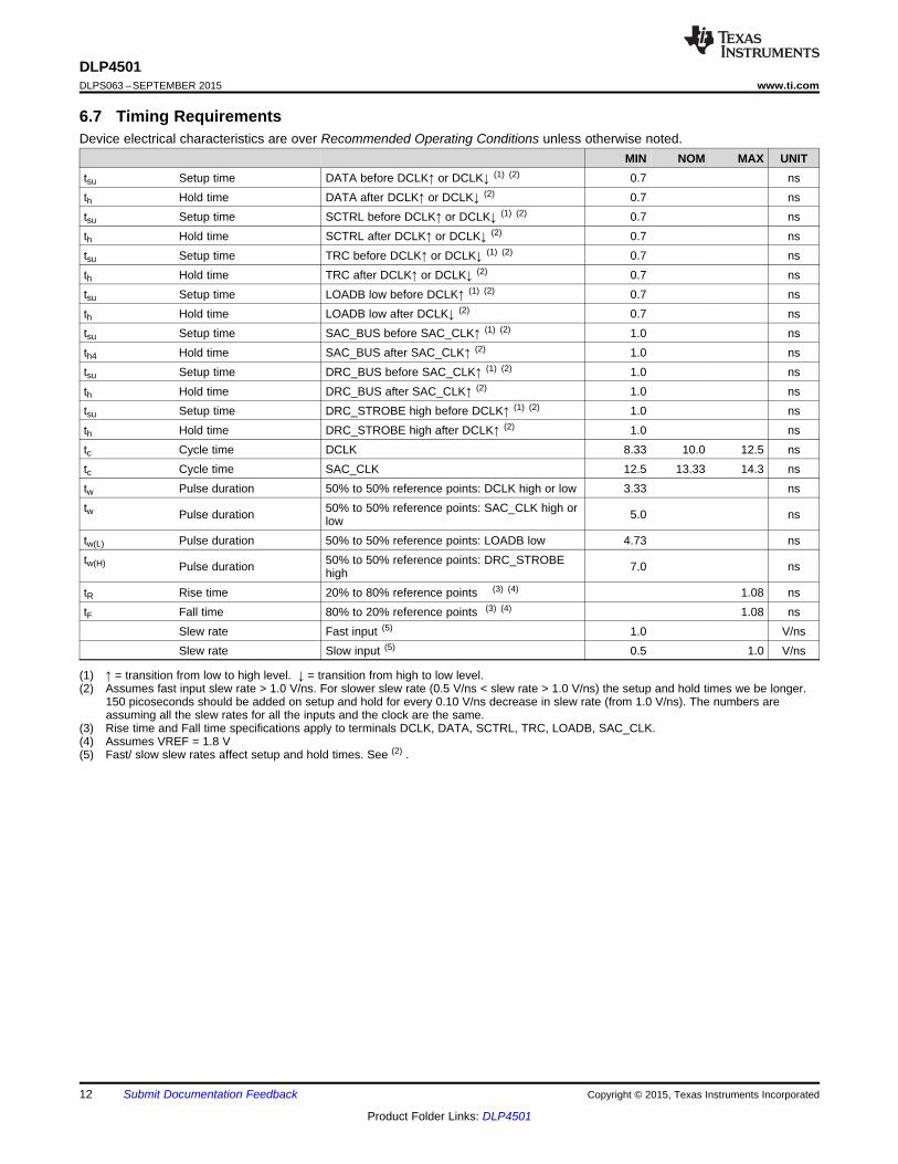
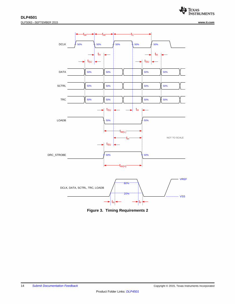
6.7 Timing RequirementsDevice electrical characteristics are over Recommended Operating Conditions unless otherwise noted.
MIN NOM MAX UNITtsu Setup time DATA before DCLK↑ or DCLK↓ (1) (2) 0.7 nsth Hold time DATA after DCLK↑ or DCLK↓ (2) 0.7 nstsu Setup time SCTRL before DCLK↑ or DCLK↓ (1) (2) 0.7 nsth Hold time SCTRL after DCLK↑ or DCLK↓ (2) 0.7 nstsu Setup time TRC before DCLK↑ or DCLK↓ (1) (2) 0.7 nsth Hold time TRC after DCLK↑ or DCLK↓ (2) 0.7 nstsu Setup time LOADB low before DCLK↑ (1) (2) 0.7 nsth Hold time LOADB low after DCLK↓ (2) 0.7 nstsu Setup time SAC_BUS before SAC_CLK↑ (1) (2) 1.0 nsth4 Hold time SAC_BUS after SAC_CLK↑ (2) 1.0 nstsu Setup time DRC_BUS before SAC_CLK↑ (1) (2) 1.0 nsth Hold time DRC_BUS after SAC_CLK↑ (2) 1.0 nstsu Setup time DRC_STROBE high before DCLK↑ (1) (2) 1.0 nsth Hold time DRC_STROBE high after DCLK↑ (2) 1.0 nstc Cycle time DCLK 8.33 10.0 12.5 nstc Cycle time SAC_CLK 12.5 13.33 14.3 nstw Pulse duration 50% to 50% reference points: DCLK high or low 3.33 nstw 50% to 50% reference points: SAC_CLK high orPulse duration 5.0 nslowtw(L) Pulse duration 50% to 50% reference points: LOADB low 4.73 nstw(H) 50% to 50% reference points: DRC_STROBEPulse duration 7.0 nshightR Rise time 20% to 80% reference points (3) (4) 1.08 nstF Fall time 80% to 20% reference points (3) (4) 1.08 ns
Slew rate Fast input (5) 1.0 V/nsSlew rate Slow input (5) 0.5 1.0 V/ns
(1) ↑ = transition from low to high level. ↓ = transition from high to low level.(2) Assumes fast input slew rate > 1.0 V/ns. For slower slew rate (0.5 V/ns < slew rate > 1.0 V/ns) the setup and hold times we be longer.
150 picoseconds should be added on setup and hold for every 0.10 V/ns decrease in slew rate (from 1.0 V/ns). The numbers areassuming all the slew rates for all the inputs and the clock are the same.
(3) Rise time and Fall time specifications apply to terminals DCLK, DATA, SCTRL, TRC, LOADB, SAC_CLK.(4) Assumes VREF = 1.8 V(5) Fast/ slow slew rates affect setup and hold times. See (2) .
12 Submit Documentation Feedback Copyright © 2015, Texas Instruments Incorporated
Product Folder Links: DLP4501

DRC_BUS
DRC_STROBE
SAC_CLK
SAC_BUS
tW(H)
tWtC
50%50%
tW
50%50% 50%
tH
tSU
50%50%
50%
50%
50%
tSU
tSU
tH
50%
tH
50%
50%
VSS20%
80%VREF
tR tF
SAC_CLKNOT TO SCALE
DLP4501www.ti.com DLPS063 –SEPTEMBER 2015
Figure 2. Timing Requirements 1
Copyright © 2015, Texas Instruments Incorporated Submit Documentation Feedback 13
Product Folder Links: DLP4501
DATA
DCLK
tCtW
50%50%50%
50%
tH
tSU
50% 50%
50% 50%
tH
tSU
SCTRL 50% 50% 50%
TRC 50% 50% 50%
50%
50%
50%
tHtSU
50%50%LOADB
VSS
VREF
20%
80%
tR tF
DCLK, DATA, SCTRL, TRC, LOADB
NOT TO SCALE
tSU
50%50%
tW(H)
DRC_STROBE
tH
tW(L)
tW
DLP4501DLPS063 –SEPTEMBER 2015 www.ti.com
Figure 3. Timing Requirements 2
14 Submit Documentation Feedback Copyright © 2015, Texas Instruments Incorporated
Product Folder Links: DLP4501

Wire Bond Cover Interface Area(allowed contact area)
Electrical Interface Area 1 Electrical Interface Area 2
Do not contact cover on any sidesThermal Interface Area
Do not contact cover in these areas
Datum ‘E’(1 area)
Datum ‘A’(3 areas)
CL
Tester ChannelOutput Under Test
Data Sheet Timing Reference Point
Device Pin
DLP4501www.ti.com DLPS063 –SEPTEMBER 2015
A. See Timing for more information.
Figure 4. Test Load Circuit for AC Timing Measurement
6.8 System Mounting Interface Loads
PARAMETER MIN NOM MAX UNITMaximum system mounting interface load to be applied to the:
79 N• Thermal Interface area (see Figure 5)
• Electrical Interface area uniformly distributed over each of the areas (Area #1 55 Nand Area #2) (see Figure 5)
60 N• Wire Bond Cover Interface Area (see Figure 5)
Figure 5. System Interface Loads
Copyright © 2015, Texas Instruments Incorporated Submit Documentation Feedback 15
Product Folder Links: DLP4501
Column 1136
Column 2
Column 0
Row
910
Row
0
Column 1138
Row
911
Row
1
Height
Width
DMD Active Array
1140 × 912 Micromirrors
Pond of Micromirrors (POM) and other details omitted for clarity. Not to scale.
Column 1
Column 3
Column 1139
Column 1137
Incident IlluminationLight Path
D
D
P P
DLP4501DLPS063 –SEPTEMBER 2015 www.ti.com
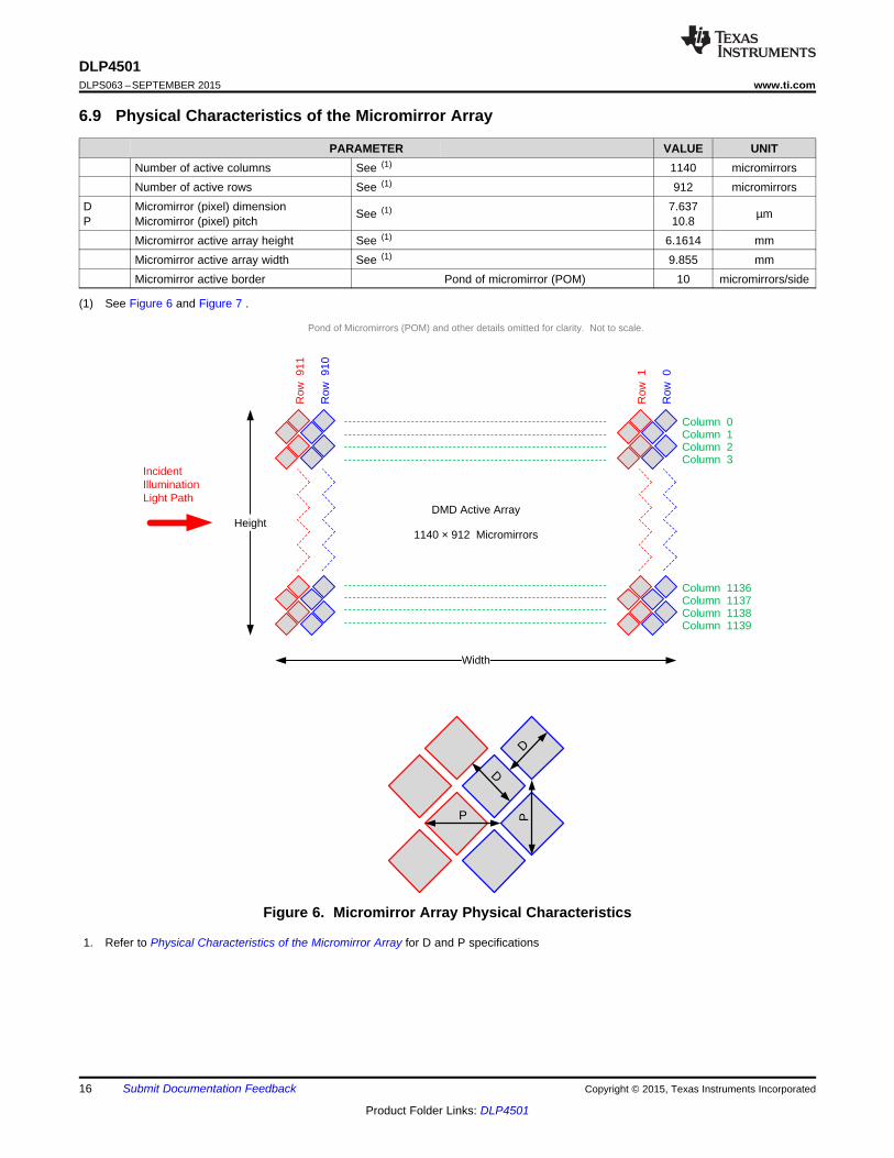
6.9 Physical Characteristics of the Micromirror Array
PARAMETER VALUE UNITNumber of active columns See (1) 1140 micromirrorsNumber of active rows See (1) 912 micromirrors
D Micromirror (pixel) dimension 7.637See (1) µmP Micromirror (pixel) pitch 10.8Micromirror active array height See (1) 6.1614 mmMicromirror active array width See (1) 9.855 mmMicromirror active border Pond of micromirror (POM) 10 micromirrors/side
(1) See Figure 6 and Figure 7 .
Figure 6. Micromirror Array Physical Characteristics
1. Refer to Physical Characteristics of the Micromirror Array for D and P specifications
16 Submit Documentation Feedback Copyright © 2015, Texas Instruments Incorporated
Product Folder Links: DLP4501
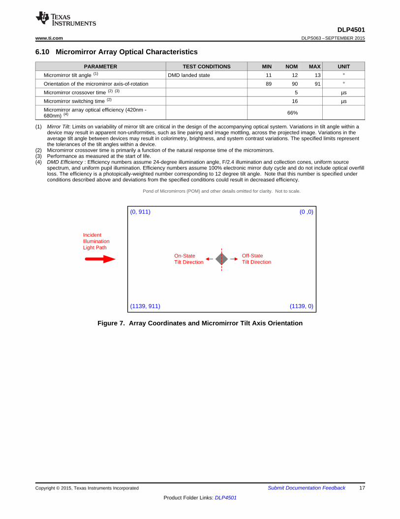
Incident IlluminationLight Path
(0 ,0)
(1139, 911)
On-StateTilt Direction
Off-StateTilt Direction
(1139, 0)
(0, 911)
Pond of Micromirrors (POM) and other details omitted for clarity. Not to scale.
DLP4501www.ti.com DLPS063 –SEPTEMBER 2015
6.10 Micromirror Array Optical Characteristics
PARAMETER TEST CONDITIONS MIN NOM MAX UNITMicromirror tilt angle (1) DMD landed state 11 12 13 °Orientation of the micromirror axis-of-rotation 89 90 91 °Micromirror crossover time (2) (3) 5 µsMicromirror switching time (2) 16 µsMicromirror array optical efficiency (420nm - 66%680nm) (4)
(1) Mirror Tilt: Limits on variability of mirror tilt are critical in the design of the accompanying optical system. Variations in tilt angle within adevice may result in apparent non-uniformities, such as line pairing and image mottling, across the projected image. Variations in theaverage tilt angle between devices may result in colorimetry, brightness, and system contrast variations. The specified limits representthe tolerances of the tilt angles within a device.
(2) Micromirror crossover time is primarily a function of the natural response time of the micromirrors.(3) Performance as measured at the start of life.(4) DMD Efficiency : Efficiency numbers assume 24-degree illumination angle, F/2.4 illumination and collection cones, uniform source
spectrum, and uniform pupil illumination. Efficiency numbers assume 100% electronic mirror duty cycle and do not include optical overfillloss. The efficiency is a photopically-weighted number corresponding to 12 degree tilt angle. Note that this number is specified underconditions described above and deviations from the specified conditions could result in decreased efficiency.
Figure 7. Array Coordinates and Micromirror Tilt Axis Orientation
Copyright © 2015, Texas Instruments Incorporated Submit Documentation Feedback 17
Product Folder Links: DLP4501

DLP4501DLPS063 –SEPTEMBER 2015 www.ti.com
6.11 Window Characteristics
PARAMETER (1) MIN NOM MAX UNITWindow material designation Corning Eagle XGWindow refractive index at wavelength 546.1 nm 1.5119Window aperture (2) See (2)
Illumination overfill (3) See (3)
Window Transmittance, single-pass Minimum within the wavelength rangethrough both surfaces and glass (4) 420 to 680 nm. Applies to all angles 0° 97%
to 30° AOI.Window Transmittance, single-pass Average over the wavelength range 420through both surfaces and glass (4) to 680 nm. Applies to all angles 30° to 97%
45° AOI.
(1) See Window Characteristics and Optics for more information.(2) See the package mechanical characteristics for details regarding the size and location of the window aperture.(3) The active area of the .45 WXGA device is surrounded by an aperture on the inside of the DMD window surface that masks structures
of the DMD device assembly from normal view. The aperture is sized to anticipate several optical conditions. Overfill light illuminatingthe area outside the active array can scatter and create adverse effects to the performance of an end application using the DMD. Theillumination optical system should be designed to limit light flux incident outside the active array to less than 10% of the average fluxlevel in the active area. Depending on the particular system's optical architecture and assembly tolerances, the amount of overfill light onthe outside of the active array may cause system performance degradation.
(4) Single-pass through both surfaces and glass
6.12 Chipset Component Usage SpecificationThe DLP4501 DMD is a component of one or more DLP chipsets. Reliable function and operation of theDLP4501 DMD requires that it be used in conjunction with the other components of the applicable DLPchipset, including those components that contain or implement TI DMD control technology. TI DMD controltechnology is the TI technology and devices for operating or controlling a DLP DMD.
NOTETI assumes no responsibility for image quality artifacts or DMD failures caused by opticalsystem operating conditions exceeding limits described previously.
18 Submit Documentation Feedback Copyright © 2015, Texas Instruments Incorporated
Product Folder Links: DLP4501
Column Read & Write
Bit
Line
s
Word Lines
(0,0)
(1139, 911)
Micromirror Array
Control
VoltageGenerators
Control
Control Control
Bit
Line
s
Row
Column Read & Write
Voltages
Channel AInterface
Channel BInterface
DA
TA
SC
TR
L
DC
LK
SA
C_C
LK
SA
C_B
US
VC
C
VO
FF
SE
T
VR
ES
ET
VB
IAS
DR
C_O
EZ
DR
C_S
TR
OB
E
Not to Scale.
LOA
DB
TR
C
VS
S
VR
EF
VC
C
VO
FF
SE
T
VR
ES
ET
VB
IAS
VS
S
VR
EF
DR
C_B
US
RE
SE
RV
ED
Details Omitted for Clarity.
DLP4501www.ti.com DLPS063 –SEPTEMBER 2015
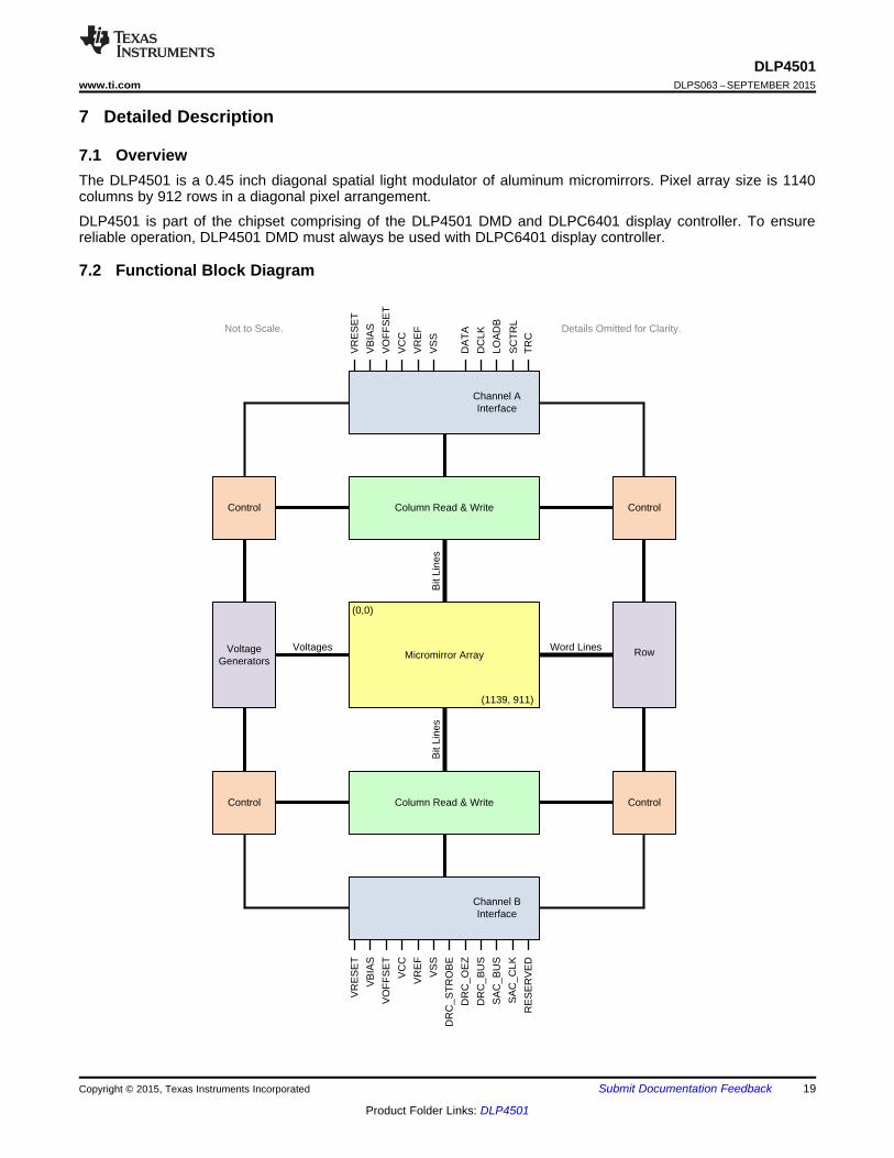
7 Detailed Description
7.1 OverviewThe DLP4501 is a 0.45 inch diagonal spatial light modulator of aluminum micromirrors. Pixel array size is 1140columns by 912 rows in a diagonal pixel arrangement.
DLP4501 is part of the chipset comprising of the DLP4501 DMD and DLPC6401 display controller. To ensurereliable operation, DLP4501 DMD must always be used with DLPC6401 display controller.
7.2 Functional Block Diagram
Copyright © 2015, Texas Instruments Incorporated Submit Documentation Feedback 19
Product Folder Links: DLP4501
DLP4501DLPS063 –SEPTEMBER 2015 www.ti.com
7.3 Feature Description
7.3.1 TimingThe data sheet provides timing at the device pin. For output timing analysis, the tester pin electronics and itstransmission line effects must be taken into account. Figure 4 shows an equivalent test load circuit for the outputunder test. Timing reference loads are not intended as a precise representation of any particular systemenvironment or depiction of the actual load presented by a production test. System designers should use IBIS orother simulation tools to correlate the timing reference load to a system environment. The load capacitance valuestated is only for characterization and measurement of AC timing signals. This load capacitance value does notindicate the maximum load the device is capable of driving.
7.4 Device Functional ModesDMD functional modes are controlled by the DLPC6401 display controller. See the DLPC6401 display controllerdata sheet or contact a TI applications engineer.
7.5 Window Characteristics and Optics
NOTETI assumes no responsibility for image quality artifacts or DMD failures caused by opticalsystem operating conditions exceeding limits described previously.
7.5.1 Optical Interface and System Image QualityTI assumes no responsibility for end-equipment optical performance. Achieving the desired end-equipmentoptical performance involves making trade-offs between numerous component and system design parameters.Optimizing system optical performance and image quality strongly relate to optical system design parametertrades. Although it is not possible to anticipate every conceivable application, projector image quality and opticalperformance is contingent on compliance to the optical system operating conditions described in the followingsections:
7.5.1.1 Numerical Aperture and Stray Light ControlThe angle defined by the numerical aperture of the illumination and projection optics at the DMD optical areashould be the same. This angle should not exceed the nominal device mirror tilt angle unless appropriateapertures are added in the illumination and/or projection pupils to block out flat-state and stray light from theprojection lens. The mirror tilt angle defines DMD capability to separate the ON optical path from any other lightpath, including undesirable flat–state specular reflections from the DMD window, DMD border structures, or othersystem surfaces near the DMD such as prism or lens surfaces. If the numerical aperture exceeds the mirror tiltangle, or if the projection numerical aperture angle is more than two degrees larger than the illuminationnumerical aperture angle, objectionable artifacts in the display’s border and/or active area could occur.
7.5.1.2 Pupil MatchTI’s optical and image quality specifications assume that the exit pupil of the illumination optics is nominallycentered within 2° of the entrance pupil of the projection optics. Misalignment of pupils can create objectionableartifacts in the display’s border and/or active area, which may require additional system apertures to control,especially if the numerical aperture of the system exceeds the pixel tilt angle.
7.5.1.3 Illumination OverfillThe active area of the device is surrounded by an aperture on the inside DMD window surface that masksstructures of the DMD chip assembly from normal view, and is sized to anticipate several optical operatingconditions. Overfill light illuminating the window aperture can create artifacts from the edge of the windowaperture opening and other surface anomalies that may be visible on the screen. The illumination optical systemshould be designed to limit light flux incident anywhere on the window aperture from exceeding approximately10% of the average flux level in the active area. Depending on the particular system’s optical architecture, overfilllight may have to be further reduced below the suggested 10% level in order to be acceptable.
20 Submit Documentation Feedback Copyright © 2015, Texas Instruments Incorporated
Product Folder Links: DLP4501
DLP4501www.ti.com DLPS063 –SEPTEMBER 2015
7.6 Micromirror Array Temperature Calculation
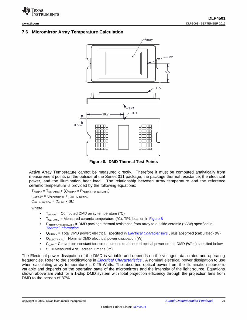
Figure 8. DMD Thermal Test Points
Active Array Temperature cannot be measured directly. Therefore it must be computed analytically frommeasurement points on the outside of the Series 311 package, the package thermal resistance, the electricalpower, and the illumination heat load. The relationship between array temperature and the referenceceramic temperature is provided by the following equations:
TARRAY = TCERAMIC + (QARRAY × RARRAY–TO–CERAMIC)QARRAY = QELECTRICAL + QILLUMINATION
QILLUMINATION = (CL2W × SL)
where• TARRAY = Computed DMD array temperature (°C)• TCERAMIC = Measured ceramic temperature (°C), TP1 location in Figure 8• RARRAY–TO–CERAMIC = DMD package thermal resistance from array to outside ceramic (°C/W) specified in
Thermal Information• QARRAY = Total DMD power; electrical, specified in Electrical Characteristics , plus absorbed (calculated) (W)• QELECTRICAL = Nominal DMD electrical power dissipation (W)• CL2W = Conversion constant for screen lumens to absorbed optical power on the DMD (W/lm) specified below• SL = Measured ANSI screen lumens (lm)
The Electrical power dissipation of the DMD is variable and depends on the voltages, data rates and operatingfrequencies. Refer to the specifications in Electrical Characteristics . A nominal electrical power dissipation to usewhen calculating array temperature is 0.25 Watts. The absorbed optical power from the illumination source isvariable and depends on the operating state of the micromirrors and the intensity of the light source. Equationsshown above are valid for a 1-chip DMD system with total projection efficiency through the projection lens fromDMD to the screen of 87%.
Copyright © 2015, Texas Instruments Incorporated Submit Documentation Feedback 21
Product Folder Links: DLP4501
DLP4501DLPS063 –SEPTEMBER 2015 www.ti.com
Micromirror Array Temperature Calculation (continued)The conversion constant CL2W is based on the DMD micromirror array characteristics. It assumes a spectralefficiency of 300 lm/W for the projected light and illumination distribution of 83.7% on the DMD active array, and16.3% on the DMD array border and window aperture. The conversion constant is calculated to be 0.00293W/lm.
Sample Calculation for typical projection application:
TCERAMIC = 55°C, assumed system measurement; see Recommended Operating Conditions for specificationlimitsSL = 1000 lmQELECTRICAL = 0.25 WCL2W = 0.00293 W/lmQARRAY = 0.025 + (0.00293 × 1000) = 3.18 WTARRAY = 55°C + (3.18 W × 2.0 °C/W) = 61.4 °C
7.7 Micromirror Landed-On/Landed-Off Duty Cycle
7.7.1 Definition of Micromirror Landed-On/Landed-Off Duty CycleThe micromirror landed-on/landed-off duty cycle (landed duty cycle) denotes the amount of time (as apercentage) that an individual micromirror is landed in the On state versus the amount of time the samemicromirror is landed in the Off state.
As an example, a landed duty cycle of 100/0 indicates that the referenced pixel is in the On state 100% of thetime (and in the Off state 0% of the time), whereas 0/100 would indicate that the pixel is in the Off state 100% ofthe time. Likewise, 50/50 indicates that the pixel is On 50% of the time and Off 50% of the time.
Note that when assessing landed duty cycle, the time spent switching from one state (ON or OFF) to the otherstate (OFF or ON) is considered negligible and is thus ignored.
Since a micromirror can only be landed in one state or the other (On or Off), the two numbers (percentages)always add to 100.
7.7.2 Landed Duty Cycle and Useful Life of the DMDKnowing the long-term average landed duty cycle (of the end product or application) is important becausesubjecting all (or a portion) of the DMD’s micromirror array (also called the active array) to an asymmetric landedduty cycle for a prolonged period of time can reduce the DMD’s usable life.
Note that it is the symmetry/asymmetry of the landed duty cycle that is of relevance. The symmetry of the landedduty cycle is determined by how close the two numbers (percentages) are to being equal. For example, a landedduty cycle of 50/50 is perfectly symmetrical whereas a landed duty cycle of 100/0 or 0/100 is perfectlyasymmetrical.
7.7.3 Landed Duty Cycle and Operational DMD TemperatureOperational DMD Temperature and Landed Duty Cycle interact to affect the DMD’s usable life, and thisinteraction can be exploited to reduce the impact that an asymmetrical Landed Duty Cycle has on the DMD’susable life. This is quantified in the de-rating curve shown in Figure 1. The importance of this curve is that:• All points along this curve represent the same usable life.• All points above this curve represent lower usable life (and the further away from the curve, the lower the
usable life).• All points below this curve represent higher usable life (and the further away from the curve, the higher the
usable life).
In practice, this curve specifies the Maximum Operating DMD Temperature that the DMD should be operated atfor a give long-term average Landed Duty Cycle.
22 Submit Documentation Feedback Copyright © 2015, Texas Instruments Incorporated
Product Folder Links: DLP4501
DLP4501www.ti.com DLPS063 –SEPTEMBER 2015
Micromirror Landed-On/Landed-Off Duty Cycle (continued)7.7.4 Estimating the Long-Term Average Landed Duty Cycle of a Product or ApplicationDuring a given period of time, the Landed Duty Cycle of a given pixel follows from the image content beingdisplayed by that pixel.
For example, in the simplest case, when displaying pure-white on a given pixel for a given time period, that pixelwill experience a 100/0 Landed Duty Cycle during that time period. Likewise, when displaying pure-black, thepixel will experience a 0/100 Landed Duty Cycle.
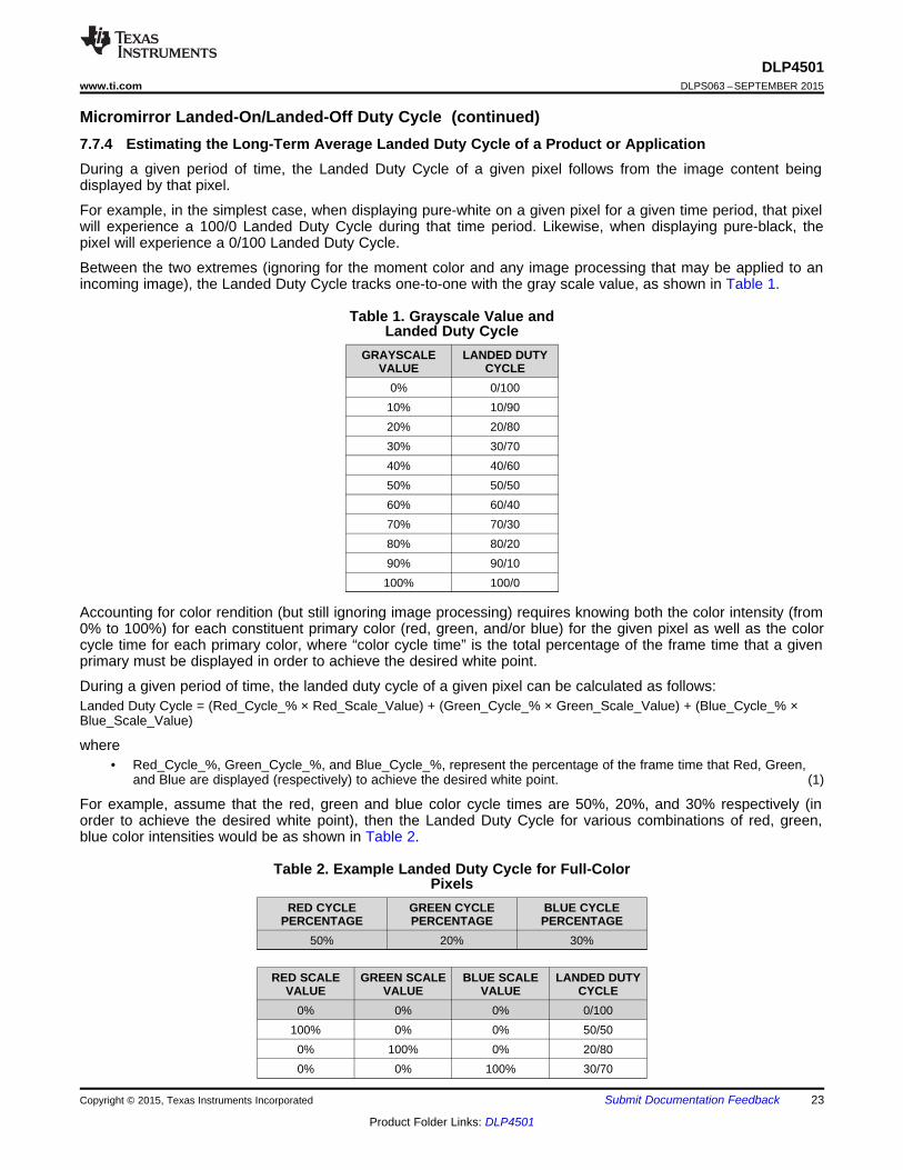
Between the two extremes (ignoring for the moment color and any image processing that may be applied to anincoming image), the Landed Duty Cycle tracks one-to-one with the gray scale value, as shown in Table 1.
Table 1. Grayscale Value andLanded Duty Cycle
GRAYSCALE LANDED DUTYVALUE CYCLE
0% 0/10010% 10/9020% 20/8030% 30/7040% 40/6050% 50/5060% 60/4070% 70/3080% 80/2090% 90/10100% 100/0
Accounting for color rendition (but still ignoring image processing) requires knowing both the color intensity (from0% to 100%) for each constituent primary color (red, green, and/or blue) for the given pixel as well as the colorcycle time for each primary color, where “color cycle time” is the total percentage of the frame time that a givenprimary must be displayed in order to achieve the desired white point.
During a given period of time, the landed duty cycle of a given pixel can be calculated as follows:Landed Duty Cycle = (Red_Cycle_% × Red_Scale_Value) + (Green_Cycle_% × Green_Scale_Value) + (Blue_Cycle_% ×Blue_Scale_Value)
where• Red_Cycle_%, Green_Cycle_%, and Blue_Cycle_%, represent the percentage of the frame time that Red, Green,
and Blue are displayed (respectively) to achieve the desired white point. (1)
For example, assume that the red, green and blue color cycle times are 50%, 20%, and 30% respectively (inorder to achieve the desired white point), then the Landed Duty Cycle for various combinations of red, green,blue color intensities would be as shown in Table 2.
Table 2. Example Landed Duty Cycle for Full-ColorPixels
RED CYCLE GREEN CYCLE BLUE CYCLEPERCENTAGE PERCENTAGE PERCENTAGE
50% 20% 30%
RED SCALE GREEN SCALE BLUE SCALE LANDED DUTYVALUE VALUE VALUE CYCLE
0% 0% 0% 0/100100% 0% 0% 50/50
0% 100% 0% 20/800% 0% 100% 30/70
Copyright © 2015, Texas Instruments Incorporated Submit Documentation Feedback 23
Product Folder Links: DLP4501
Input Level (%)
Out
put L
evel
(%
)
0 10 20 30 40 50 60 70 80 90 1000
10
20
30
40
50
60
70
80
90
100
D002
Gamma = 2.2
DLP4501DLPS063 –SEPTEMBER 2015 www.ti.com
RED SCALE GREEN SCALE BLUE SCALE LANDED DUTYVALUE VALUE VALUE CYCLE
12% 0% 0% 6/940% 35% 0% 7/930% 0% 60% 18/82
100% 100% 0% 70/300% 100% 100% 50/50
100% 0% 100% 80/2012% 35% 0% 13/870% 35% 60% 25/75
12% 0% 60% 24/76100% 100% 100% 100/0
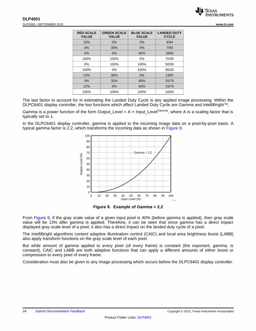
The last factor to account for in estimating the Landed Duty Cycle is any applied image processing. Within theDLPC6401 display controller, the two functions which affect Landed Duty Cycle are Gamma and IntelliBright™.
Gamma is a power function of the form Output_Level = A × Input_LevelGamma, where A is a scaling factor that istypically set to 1.
In the DLPC6401 display controller, gamma is applied to the incoming image data on a pixel-by-pixel basis. Atypical gamma factor is 2.2, which transforms the incoming data as shown in Figure 9.
Figure 9. Example of Gamma = 2.2
From Figure 9, if the gray scale value of a given input pixel is 40% (before gamma is applied), then gray scalevalue will be 13% after gamma is applied. Therefore, it can be seen that since gamma has a direct impactdisplayed gray scale level of a pixel, it also has a direct impact on the landed duty cycle of a pixel.
The IntelliBright algorithms content adaptive illumination control (CAIC) and local area brightness boost (LABB)also apply transform functions on the gray scale level of each pixel.
But while amount of gamma applied to every pixel (of every frame) is constant (the exponent, gamma, isconstant), CAIC and LABB are both adaptive functions that can apply a different amounts of either boost orcompression to every pixel of every frame.
Consideration must also be given to any image processing which occurs before the DLPC6401 display controller.
24 Submit Documentation Feedback Copyright © 2015, Texas Instruments Incorporated
Product Folder Links: DLP4501
Included in DLP® Chipset
Port 2
LVDS (Flat Panel Display
Link Compatible)
Port
VGA
Composite, Component,
SVideo
HDMI
Port 1
30 bit Parallel
I2C
LED
(R, G, B, HS, VS, clk)
I2C
I2C
I2CLVDS
24
DLP4501 DMD
(.45 WXGA)
GPIO IR USB RS232
DDR
LEDI2C
12V DC Supply Regulators to generate different
power supply used in system.
3.3V, 5V, 1.2V, 1.9V, 8.5V, -10V, 16V
(WiFi Display)
Display Port DLP Controller ASIC
(Internal Frame Memory)
Analog
Front End
HDMI
Receiver/
Display Port
Receiver
Parallel
FlashEPROM
DLPC6401
(23mm x 23mm)- 1Watt
Multimedia
Front End
Discrete LED Driver
DLP4501
(WXGA
DMD)
DLP4501www.ti.com DLPS063 –SEPTEMBER 2015
8 Application and Implementation
NOTEInformation in the following applications sections is not part of the TI componentspecification, and TI does not warrant its accuracy or completeness. TI’s customers areresponsible for determining suitability of components for their purposes. Customers shouldvalidate and test their design implementation to confirm system functionality.
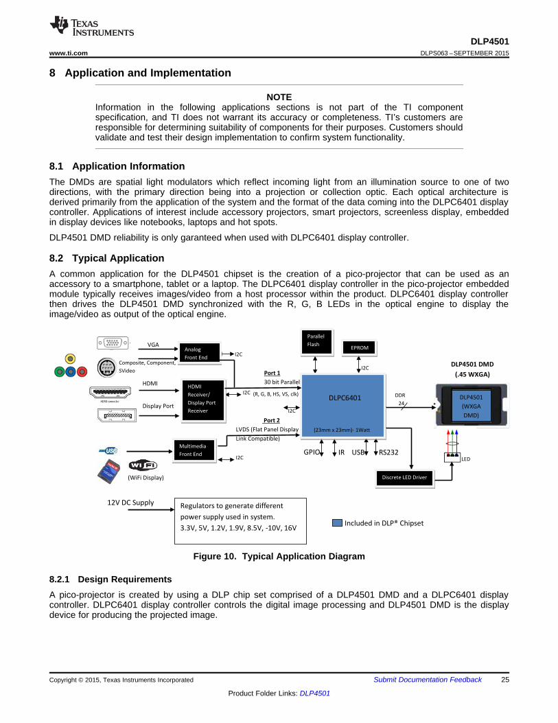
8.1 Application InformationThe DMDs are spatial light modulators which reflect incoming light from an illumination source to one of twodirections, with the primary direction being into a projection or collection optic. Each optical architecture isderived primarily from the application of the system and the format of the data coming into the DLPC6401 displaycontroller. Applications of interest include accessory projectors, smart projectors, screenless display, embeddedin display devices like notebooks, laptops and hot spots.
DLP4501 DMD reliability is only garanteed when used with DLPC6401 display controller.
8.2 Typical ApplicationA common application for the DLP4501 chipset is the creation of a pico-projector that can be used as anaccessory to a smartphone, tablet or a laptop. The DLPC6401 display controller in the pico-projector embeddedmodule typically receives images/video from a host processor within the product. DLPC6401 display controllerthen drives the DLP4501 DMD synchronized with the R, G, B LEDs in the optical engine to display theimage/video as output of the optical engine.
Figure 10. Typical Application Diagram
8.2.1 Design RequirementsA pico-projector is created by using a DLP chip set comprised of a DLP4501 DMD and a DLPC6401 displaycontroller. DLPC6401 display controller controls the digital image processing and DLP4501 DMD is the displaydevice for producing the projected image.
Copyright © 2015, Texas Instruments Incorporated Submit Documentation Feedback 25
Product Folder Links: DLP4501
DLP4501DLPS063 –SEPTEMBER 2015 www.ti.com
Typical Application (continued)In addition to the two DLP chips in the chip set, other chips may be needed. Typically a Flash part is needed tostore the software and firmware. Also a discrete LED driver solution is required to provide the LED driverfunctionality for LED illumination. The illumination light that is applied to the DMD is typically from red, green, andblue LEDs. These are often contained in three separate packages, but sometimes more than one color of LEDdie may be in the same package to reduce the overall size of the pico-projector. DLPC6401 display controllerprovides either parallel or LVDS interface to connect the DLPC6401 display controller to the multimedia front endfor receiving images and video.
8.2.2 Detailed Design ProcedureFor connecting together the DLPC6401 display controller and the DLP4501 DMD, see the reference designschematic. Layout guidelines should be followed to achieve a reliable projector. To complete the DLP system anoptical module or light engine is required that contains the DLP4501 DMD, associated illumination sources,optical elements, and necessary mechanical components.
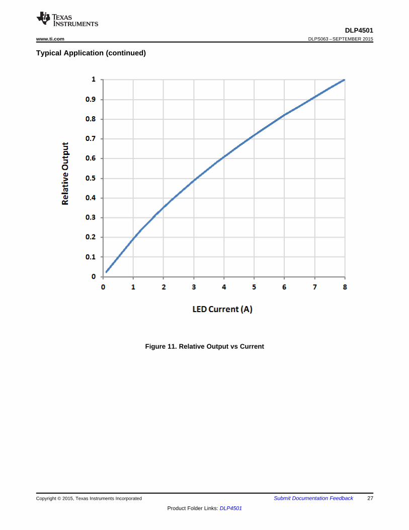
8.2.3 Application CurveAs the LED currents that are driven time-sequentially through the red, green, and blue LEDs are increased, thebrightness of the projector increases. This increase is non-linear, and the curve for typical relative outputchanges with LED currents is shown in Figure 11. For the LED currents shown, it is assumed that the samecurrent amplitude is applied to the red, green, and blue.
SPACE
26 Submit Documentation Feedback Copyright © 2015, Texas Instruments Incorporated
Product Folder Links: DLP4501
DLP4501www.ti.com DLPS063 –SEPTEMBER 2015
Typical Application (continued)
Figure 11. Relative Output vs Current
Copyright © 2015, Texas Instruments Incorporated Submit Documentation Feedback 27
Product Folder Links: DLP4501
DLP4501DLPS063 –SEPTEMBER 2015 www.ti.com
9 Power Supply RecommendationsThe DLP4501 requires VBIAS, VCC, VREF, VOFFSET, and VRESET power supplies . Common ground VSSmust also be connected. DMD power-up and power-down sequencing is strictly controlled by the DLPC6401display controller.
Previous DMDs using external reset waveform drivers have required VCC, VREF, and VOFFSET (sometimesreferred to as VCC2) power supplies. Because the DLP4501 generates its own reset waveforms, the additionalpower supplies VBIAS and VRESET must also be supplied to the DMD. VBIAS, VCC, VREF, VOFFSET, andVRESET power supplies must be coordinated during power-up and power-down operations. Common groundVSS must also be connected.
CAUTIONFor reliable operation of the DMD, the following power supply sequencingrequirements must be followed. Failure to adhere to the prescribed power-up andpower-down procedures may affect device reliability.
VCC, VREF, VOFFSET, VBIAS, and VRESET power supplies have to be coordinatedduring power-up and power-down operations. Failure to meet any of the belowrequirements will result in a significant reduction in the DMD’s reliability and lifetime.VSS must also be connected.
9.1 Power Supply Power-Up Procedure• During power-up, VCC and VREF must always start and settle before VOFFSET specified in Table 3, VBIAS,
and VRESET voltages are applied to the DMD.• During power-up, it is a strict requirement that the delta between VBIAS and VOFFSET must be within the
specified limit shown in Recommended Operating Conditions. Refer to Table 3 and the Layout Example forpower-up delay requirements.
• During power-up, LVCMOS input pins shall not be driven high until after VCC and VREF have settled atoperating voltages listed in Recommended Operating Conditions
• Power supply slew rates during power-up are flexible, provided that the transient voltage levels follow therequirements specified in Absolute Maximum Ratings , in Recommended Operating Conditions and inFigure 12.
9.2 Power Supply Power-Down Procedure• Power-down sequence is the reverse order of the previous power-up sequence. VCC and VREF must be
supplied until after VBIAS, VRESET, and VOFFSET are discharged to within 4 V of ground.• During power-down, it is not mandatory to stop driving VBIAS prior to VOFFSET, but it is a strict requirement
that the delta between VBIAS and VOFFSET must be within the specified limit shown in RecommendedOperating Conditions (Refer to Note 2 for Figure 12).
• During power-down, LVCMOS input pins must be less than specified in Recommended Operating Conditions.• During power-down, there is no requirement for the relative timing of VRESET with respect to VOFFSET and
VBIAS.• Power supply slew rates during power-down are flexible, provided that the transient voltage levels follow the
requirements specified in Absolute Maximum Ratings, in Recommended Operating Conditions and inFigure 12.
28 Submit Documentation Feedback Copyright © 2015, Texas Instruments Incorporated
Product Folder Links: DLP4501
Mirror Park SequenceVSSDRC_OEZ
VCC / VREF
Power OffVBIAS, VOFFSET, and VRESET are disabled by DLP Controller software
VRESET
VRESET
VRESET < Specification
VRESET > Specification
VSS
VRESET
VOFFSET
VSS
VOFFSET
VOFFSETNote 2
ûV < Specification
VOFFSET < Specification
VBIAS
VBIAS
VSSVSS
VBIAS
VBIAS < Specification
Not to Scale. Details Omitted for Clarity.
VSS
VSS
VCC / VREF
VSSVSSVCC / VREF
VCC / VREF
VSSLVCMOS Inputs
VSS
Note 5
Note 5
Note 5
Note 1
VSS
Note 3
Note 4
DLP4501www.ti.com DLPS063 –SEPTEMBER 2015
9.3 Power Supply Sequencing Requirements
(1) See Absolute Maximum Ratings, Recommended Operating Conditions, and Package Pin Functions. Figure 12 is notto scale and details have been omitted for clarity.
(2) To prevent excess current, the supply voltage delta |VBIAS – VOFFSET| must be less than specified inRecommended Operating Conditions. OEMs may find that the most reliable way to ensure this is to power VOFFSETprior to VBIAS during power-up and to remove VBIAS prior to VOFFSET during power-down..
(3) During the mirror parking process, VBIAS, VRESET, VOFFSET, VCC, VREF, and VSS power supplies are allrequired to be within specifications listed in Recommended Operating Conditions. Once the mirrors are parked,VBIAS, VRESET, and VOFFSET may be turned off. Then, VCC, VREF, and VSS power supplies may remainenabled or be turned off.
(4) When system power is interrupted, the DLP Controller initiates hardware power-down that disables VBIAS, VRESETand VOFFSET after the micromirror park sequence. VBIAS, VRESET and VOFFSET are disabled after the mirrorpark sequence through software control.
(5) Refer to the DMD Power-Down Sequence Requirements table for specifications.
Figure 12. Power Supply Sequencing Requirements (Power Up and Power Down)
Copyright © 2015, Texas Instruments Incorporated Submit Documentation Feedback 29
Product Folder Links: DLP4501
DLP4501DLPS063 –SEPTEMBER 2015 www.ti.com
Table 3. Power-Up Sequence Delay RequirementPARAMETER MIN MAX UNIT
VBIAS Supply voltage level during power–down sequence 4.0 VVOFFSET Supply voltage level during power–down sequence 4.0 VVRESET Supply voltage level during power–down sequence –4.0 0.5 V
30 Submit Documentation Feedback Copyright © 2015, Texas Instruments Incorporated
Product Folder Links: DLP4501
DLP4501www.ti.com DLPS063 –SEPTEMBER 2015
10 Layout
10.1 Layout GuidelinesThere are no specific layout guidelines for the DMD as typically DMD is connected using a board to boardconnector to a flex cable. Flex cable provides the interface of data and Ctrl signals between the DLPC6401display controller and the DLP4501 DMD. For detailed layout guidelines refer to the layout design files. Somelayout guideline for the flex cable interface with DMD are:• Minimum of 100-nF decoupling capacitor close to VBIAS. Capacitor C5 in Figure 13.• Minimum of 100-nF decoupling capacitor close to VRST. Capacitor C4 in Figure 13.• Minimum of 100-nF decoupling capacitor close to VOFS. Capacitor C3 in Figure 13.• Minimum of 100-nF decoupling capacitor close to both groups of VCC pins, for a total of 200-nF for VCC.
Capacitor C1/C6 in Figure 13.• Minimum of 100-nF decoupling capacitor close to VREF. Capacitor C2 in Figure 13.
10.2 Layout Example
Figure 13. Power Supply Connections
Copyright © 2015, Texas Instruments Incorporated Submit Documentation Feedback 31
Product Folder Links: DLP4501
-
Two-dimensional Matrix Code(DMD part number and lot
trace code)
DMD Part Number Lot Trace Code
Device Status
Diagonal Size Desigation
Device Characteristics as Defined
Image Quality
Package Type
1 1 9 1* Å 4 b b c F
DLP4501DLPS063 –SEPTEMBER 2015 www.ti.com
11 Device and Documentation Support
11.1 Device Support
11.1.1 Device Nomenclature
Figure 14. Part Number Description
Device Status:A lead alpha character of “X” implies the device has been released for restricted sales only.
When no lead alpha character (*) is present, the device has been released for unrestricted sales.
11.1.2 Device MarkingsDevice Marking will include the human–readable character string GHJJJJK 1191-4bbcF. GHJJJJK is the lot tracecode. 1191-4bbcF is the device part number
Figure 15. DMD Marking
11.2 Related LinksThe table below lists quick access links. Categories include technical documents, support and communityresources, tools and software, and quick access to sample or buy.
Table 4. Related LinksTECHNICAL TOOLS & SUPPORT &PARTS PRODUCT FOLDER SAMPLE & BUY DOCUMENTS SOFTWARE COMMUNITY
DLP4501 Click here Click here Click here Click here Click hereDLPC6401 Click here Click here Click here Click here Click here
32 Submit Documentation Feedback Copyright © 2015, Texas Instruments Incorporated
Product Folder Links: DLP4501
DLP4501www.ti.com DLPS063 –SEPTEMBER 2015
11.3 Community ResourcesThe following links connect to TI community resources. Linked contents are provided "AS IS" by the respectivecontributors. They do not constitute TI specifications and do not necessarily reflect TI's views; see TI's Terms ofUse.
TI E2E™ Online Community TI's Engineer-to-Engineer (E2E) Community. Created to foster collaborationamong engineers. At e2e.ti.com, you can ask questions, share knowledge, explore ideas and helpsolve problems with fellow engineers.
Design Support TI's Design Support Quickly find helpful E2E forums along with design support tools andcontact information for technical support.
11.4 TrademarksIntelliBright, E2E are trademarks of Texas Instruments.DLP is a registered trademark of Texas Instruments.All other trademarks are the property of their respective owners.
11.5 Electrostatic Discharge CautionThese devices have limited built-in ESD protection. The leads should be shorted together or the device placed in conductive foamduring storage or handling to prevent electrostatic damage to the MOS gates.
11.6 GlossarySLYZ022 — TI Glossary.
This glossary lists and explains terms, acronyms, and definitions.
12 Mechanical, Packaging, and Orderable InformationThe following pages include mechanical, packaging, and orderable information. This information is the mostcurrent data available for the designated devices. This data is subject to change without notice and revision ofthis document. For browser-based versions of this data sheet, refer to the left-hand navigation.
Copyright © 2015, Texas Instruments Incorporated Submit Documentation Feedback 33
Product Folder Links: DLP4501
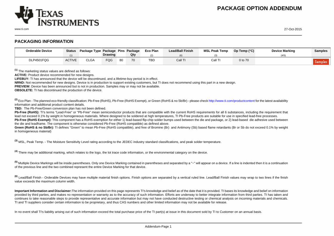
PACKAGE OPTION ADDENDUM
www.ti.com 27-Oct-2015
Addendum-Page 1
PACKAGING INFORMATION
Orderable Device Status(1)
Package Type PackageDrawing
Pins PackageQty
Eco Plan(2)
Lead/Ball Finish(6)
MSL Peak Temp(3)
Op Temp (°C) Device Marking(4/5)
Samples
DLP4501FQG ACTIVE CLGA FQG 80 70 TBD Call TI Call TI 0 to 70
(1) The marketing status values are defined as follows:ACTIVE: Product device recommended for new designs.LIFEBUY: TI has announced that the device will be discontinued, and a lifetime-buy period is in effect.NRND: Not recommended for new designs. Device is in production to support existing customers, but TI does not recommend using this part in a new design.PREVIEW: Device has been announced but is not in production. Samples may or may not be available.OBSOLETE: TI has discontinued the production of the device.
(2) Eco Plan - The planned eco-friendly classification: Pb-Free (RoHS), Pb-Free (RoHS Exempt), or Green (RoHS & no Sb/Br) - please check http://www.ti.com/productcontent for the latest availabilityinformation and additional product content details.TBD: The Pb-Free/Green conversion plan has not been defined.Pb-Free (RoHS): TI's terms "Lead-Free" or "Pb-Free" mean semiconductor products that are compatible with the current RoHS requirements for all 6 substances, including the requirement thatlead not exceed 0.1% by weight in homogeneous materials. Where designed to be soldered at high temperatures, TI Pb-Free products are suitable for use in specified lead-free processes.Pb-Free (RoHS Exempt): This component has a RoHS exemption for either 1) lead-based flip-chip solder bumps used between the die and package, or 2) lead-based die adhesive used betweenthe die and leadframe. The component is otherwise considered Pb-Free (RoHS compatible) as defined above.Green (RoHS & no Sb/Br): TI defines "Green" to mean Pb-Free (RoHS compatible), and free of Bromine (Br) and Antimony (Sb) based flame retardants (Br or Sb do not exceed 0.1% by weightin homogeneous material)
(3) MSL, Peak Temp. - The Moisture Sensitivity Level rating according to the JEDEC industry standard classifications, and peak solder temperature.
(4) There may be additional marking, which relates to the logo, the lot trace code information, or the environmental category on the device.
(5) Multiple Device Markings will be inside parentheses. Only one Device Marking contained in parentheses and separated by a "~" will appear on a device. If a line is indented then it is a continuationof the previous line and the two combined represent the entire Device Marking for that device.
(6) Lead/Ball Finish - Orderable Devices may have multiple material finish options. Finish options are separated by a vertical ruled line. Lead/Ball Finish values may wrap to two lines if the finishvalue exceeds the maximum column width.
Important Information and Disclaimer:The information provided on this page represents TI's knowledge and belief as of the date that it is provided. TI bases its knowledge and belief on informationprovided by third parties, and makes no representation or warranty as to the accuracy of such information. Efforts are underway to better integrate information from third parties. TI has taken andcontinues to take reasonable steps to provide representative and accurate information but may not have conducted destructive testing or chemical analysis on incoming materials and chemicals.TI and TI suppliers consider certain information to be proprietary, and thus CAS numbers and other limited information may not be available for release.
In no event shall TI's liability arising out of such information exceed the total purchase price of the TI part(s) at issue in this document sold by TI to Customer on an annual basis.
PACKAGE OPTION ADDENDUM
www.ti.com 27-Oct-2015
Addendum-Page 2
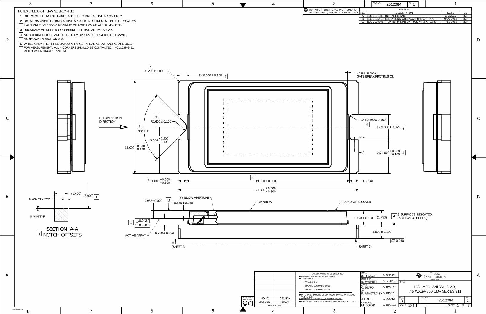
SECTION A-ANOTCH OFFSETS
2 1345678
D
C
B
A
DWG NO. SH8 7 6 5 4 3 1
D
C
B
A
INV11-2006a
2512084 1
TITLE
SIZE DWG NO REV
SCALE SHEET OF
DATE
ENGINEER
QA/CE
CM
APPROVED
DRAWN
INSTRUMENTSDallas Texas
APPLICATIONNEXT ASSY USED ON
THIRD ANGLEPROJECTION
TEXASUNLESS OTHERWISE SPECIFIEDDIMENSIONS ARE IN MILLIMETERSTOLERANCES: ANGLES 1
2 PLACE DECIMALS 0.25
1 PLACE DECIMALS 0.50DIMENSIONAL LIMITS APPLY BEFORE PROCESSESINTERPRET DIMENSIONS IN ACCORDANCE WITH ASME Y14.5M-1994REMOVE ALL BURRS AND SHARP EDGESPARENTHETICAL INFORMATION FOR REFERENCE ONLY
ICD, MECHANICAL, DMD,.45 WXGA-800 DDR SERIES 311
25120841 3
CD
1/9/2012
15:1
C. BEARD
F. ARMSTRONG
M. DORAK
1/12/2012
1/13/2012
1/10/2012
1/9/2012
NONE 0314DA
B. HASKETT
NOTES UNLESS OTHERWISE SPECIFIED:REVISIONSCOPYRIGHT 2012 TEXAS INSTRUMENTS
UN-PUBLISHED, ALL RIGHTS RESERVED.C
B. HASKETT
J. HALL 1/9/2012
EE
A
A
REV DESCRIPTION DATE BYA ECO 2121536: INITIAL RELEASE 1/9/2012 BMHB ECO 2125510: RELAX BOND WIRE COVER HEIGHT TOL 6/20/2012 BMHC ECO 2125965: TIGHTEN DIE HEIGHT TOL, WAS +/-0.080 7/11/2012 BMH
4
4
44
1
3 SURFACES INDICATEDIN VIEW B (SHEET 2)
(ILLUMINATIONDIRECTION)
DIE PARALLELISM TOLERANCE APPLIES TO DMD ACTIVE ARRAY ONLY.
ROTATION ANGLE OF DMD ACTIVE ARRAY IS A REFINEMENT OF THE LOCATIONTOLERANCE AND HAS A MAXIMUM ALLOWED VALUE OF 0.6 DEGREES.
BOUNDARY MIRRORS SURROUNDING THE DMD ACTIVE ARRAY.
NOTCH DIMENSIONS ARE DEFINED BY UPPERMOST LAYERS OF CERAMIC,AS SHOWN IN SECTION A-A.
WHILE ONLY THE THREE DATUM A TARGET AREAS A1, A2, AND A3 ARE USEDFOR MEASUREMENT, ALL 4 CORNERS SHOULD BE CONTACTED, INCLUDING E1,WHEN MOUNTING IN SYSTEM.
1
2
3
4
5
(SHEET 3) (SHEET 3)
4
4
4
4
1.6000.100
(1.733)
0.7800.063
0.953±0.0790.6500.050
WINDOW APERTURE
ACTIVE ARRAY
D
A
0.060
21.300 - 0.1000.300+
11.000 - 0.1000.300+
90°1°
5.500 - 0.1000.200+
1.000 - 0.1000.200+ 19.3000.100
3.0000.0752X
4.000 - 0.1000.200+2X
(1.000)
0.8000.1002X
(1.600)
0.400 MIN TYP.
0 MIN TYP.0.042 A
0.020 D
4
4
(3.000)
4
WINDOW
0.600R 0.100
0.200R 0.050
0.400R 0.1002X
1.6200.160
BOND WIRE COVER
0.100 MAX2X GATE BREAK PROTRUSION
VIEW BDATUMS A, B, C, AND E
SCALE 15 : 1(FROM SHEET 1)
VIEW CBOND WIRE COVER X/Y DIMENSIONS
SCALE 15 : 1(FROM SHEET 1)
2 1345678
D
C
B
A
DWG NO. SH8 7 6 5 4 3 1
D
C
B
A
INV11-2006a
2512084 2
SIZE DWG NO REV
SCALE SHEET OF
DATE
INSTRUMENTSDallas Texas
TEXASDRAWN
25120842 3
CDB. HASKETT 1/9/2012
1.500
B
19.3002X
1.500
(3.250)4X
C
A1
A2A3
E15
(1.000)4X
18.8000.100
10.6000.100
4X (R0.7)
0.300 A B C
0.300 A B C
2.2504X
0.8122X
5.300
1.038
VIEW E-EBACK SIDE METALLIZATION
(FROM SHEET 1)
DETAIL FAPERTURE SHORT EDGES
SCALE 50 : 1
2 1345678
D
C
B
A
DWG NO. SH8 7 6 5 4 3 1
D
C
B
A
INV11-2006a
2512084 3
SIZE DWG NO REV
SCALE SHEET OF
DATE
INSTRUMENTSDallas Texas
TEXASDRAWN
25120843 3
CDB. HASKETT 1/9/2012
F
VIEW DWINDOW AND ACTIVE ARRAY
(FROM SHEET 1)
3
2
0.200 A B C0.100 A
22 21 20 19 (18)
CL LC
LC
LC
1.500
6.4210.089
(6.681)APERTURE
0.2600.089
(9.855)ACTIVE ARRAY
(0.108)4X 5.5880.075
3.0810.075
(10.450)APERTURE
0.3760.089 10.0740.089
2.1510.050 11.8500.050
1.2400.050
7.4000.0501.500
(6.1614)ACTIVE ARRAY
BC
(0.068) TYP.
1.500
6.6789 x 0.742 =
8.960.25 30.25
70.25
2.671 2.2263 x 0.742 =
(5) 4 3 2 1
K
J
H
G
F
E
D
C
B
A
16.027 2.2263 x 0.742 =
BACK INDEX MARK
SYMBOLIZATION PAD
B
(42°) TYP.
(42°) TYP.
80X LGA PADS
0.6000.060 X 0.6000.060
(18X TEST PADS)
(0.742) (0.742)
(0.188)
APERTURE DIMENSIONS TO CENTER LINE OF ZIGZAG PATTERN
(8.640)WINDOW
3.50.25
(14.001)WINDOW
3.33910X
1.500
C
(0.150) TYP.
IMPORTANT NOTICE
Texas Instruments Incorporated (TI) reserves the right to make corrections, enhancements, improvements and other changes to itssemiconductor products and services per JESD46, latest issue, and to discontinue any product or service per JESD48, latest issue. Buyersshould obtain the latest relevant information before placing orders and should verify that such information is current and complete.TI’s published terms of sale for semiconductor products (http://www.ti.com/sc/docs/stdterms.htm) apply to the sale of packaged integratedcircuit products that TI has qualified and released to market. Additional terms may apply to the use or sale of other types of TI products andservices.Reproduction of significant portions of TI information in TI data sheets is permissible only if reproduction is without alteration and isaccompanied by all associated warranties, conditions, limitations, and notices. TI is not responsible or liable for such reproduceddocumentation. Information of third parties may be subject to additional restrictions. Resale of TI products or services with statementsdifferent from or beyond the parameters stated by TI for that product or service voids all express and any implied warranties for theassociated TI product or service and is an unfair and deceptive business practice. TI is not responsible or liable for any such statements.Buyers and others who are developing systems that incorporate TI products (collectively, “Designers”) understand and agree that Designersremain responsible for using their independent analysis, evaluation and judgment in designing their applications and that Designers havefull and exclusive responsibility to assure the safety of Designers' applications and compliance of their applications (and of all TI productsused in or for Designers’ applications) with all applicable regulations, laws and other applicable requirements. Designer represents that, withrespect to their applications, Designer has all the necessary expertise to create and implement safeguards that (1) anticipate dangerousconsequences of failures, (2) monitor failures and their consequences, and (3) lessen the likelihood of failures that might cause harm andtake appropriate actions. Designer agrees that prior to using or distributing any applications that include TI products, Designer willthoroughly test such applications and the functionality of such TI products as used in such applications.TI’s provision of technical, application or other design advice, quality characterization, reliability data or other services or information,including, but not limited to, reference designs and materials relating to evaluation modules, (collectively, “TI Resources”) are intended toassist designers who are developing applications that incorporate TI products; by downloading, accessing or using TI Resources in anyway, Designer (individually or, if Designer is acting on behalf of a company, Designer’s company) agrees to use any particular TI Resourcesolely for this purpose and subject to the terms of this Notice.TI’s provision of TI Resources does not expand or otherwise alter TI’s applicable published warranties or warranty disclaimers for TIproducts, and no additional obligations or liabilities arise from TI providing such TI Resources. TI reserves the right to make corrections,enhancements, improvements and other changes to its TI Resources. TI has not conducted any testing other than that specificallydescribed in the published documentation for a particular TI Resource.Designer is authorized to use, copy and modify any individual TI Resource only in connection with the development of applications thatinclude the TI product(s) identified in such TI Resource. NO OTHER LICENSE, EXPRESS OR IMPLIED, BY ESTOPPEL OR OTHERWISETO ANY OTHER TI INTELLECTUAL PROPERTY RIGHT, AND NO LICENSE TO ANY TECHNOLOGY OR INTELLECTUAL PROPERTYRIGHT OF TI OR ANY THIRD PARTY IS GRANTED HEREIN, including but not limited to any patent right, copyright, mask work right, orother intellectual property right relating to any combination, machine, or process in which TI products or services are used. Informationregarding or referencing third-party products or services does not constitute a license to use such products or services, or a warranty orendorsement thereof. Use of TI Resources may require a license from a third party under the patents or other intellectual property of thethird party, or a license from TI under the patents or other intellectual property of TI.TI RESOURCES ARE PROVIDED “AS IS” AND WITH ALL FAULTS. TI DISCLAIMS ALL OTHER WARRANTIES ORREPRESENTATIONS, EXPRESS OR IMPLIED, REGARDING RESOURCES OR USE THEREOF, INCLUDING BUT NOT LIMITED TOACCURACY OR COMPLETENESS, TITLE, ANY EPIDEMIC FAILURE WARRANTY AND ANY IMPLIED WARRANTIES OFMERCHANTABILITY, FITNESS FOR A PARTICULAR PURPOSE, AND NON-INFRINGEMENT OF ANY THIRD PARTY INTELLECTUALPROPERTY RIGHTS. TI SHALL NOT BE LIABLE FOR AND SHALL NOT DEFEND OR INDEMNIFY DESIGNER AGAINST ANY CLAIM,INCLUDING BUT NOT LIMITED TO ANY INFRINGEMENT CLAIM THAT RELATES TO OR IS BASED ON ANY COMBINATION OFPRODUCTS EVEN IF DESCRIBED IN TI RESOURCES OR OTHERWISE. IN NO EVENT SHALL TI BE LIABLE FOR ANY ACTUAL,DIRECT, SPECIAL, COLLATERAL, INDIRECT, PUNITIVE, INCIDENTAL, CONSEQUENTIAL OR EXEMPLARY DAMAGES INCONNECTION WITH OR ARISING OUT OF TI RESOURCES OR USE THEREOF, AND REGARDLESS OF WHETHER TI HAS BEENADVISED OF THE POSSIBILITY OF SUCH DAMAGES.Unless TI has explicitly designated an individual product as meeting the requirements of a particular industry standard (e.g., ISO/TS 16949and ISO 26262), TI is not responsible for any failure to meet such industry standard requirements.Where TI specifically promotes products as facilitating functional safety or as compliant with industry functional safety standards, suchproducts are intended to help enable customers to design and create their own applications that meet applicable functional safety standardsand requirements. Using products in an application does not by itself establish any safety features in the application. Designers mustensure compliance with safety-related requirements and standards applicable to their applications. Designer may not use any TI products inlife-critical medical equipment unless authorized officers of the parties have executed a special contract specifically governing such use.Life-critical medical equipment is medical equipment where failure of such equipment would cause serious bodily injury or death (e.g., lifesupport, pacemakers, defibrillators, heart pumps, neurostimulators, and implantables). Such equipment includes, without limitation, allmedical devices identified by the U.S. Food and Drug Administration as Class III devices and equivalent classifications outside the U.S.TI may expressly designate certain products as completing a particular qualification (e.g., Q100, Military Grade, or Enhanced Product).Designers agree that it has the necessary expertise to select the product with the appropriate qualification designation for their applicationsand that proper product selection is at Designers’ own risk. Designers are solely responsible for compliance with all legal and regulatoryrequirements in connection with such selection.Designer will fully indemnify TI and its representatives against any damages, costs, losses, and/or liabilities arising out of Designer’s non-compliance with the terms and provisions of this Notice.
Mailing Address: Texas Instruments, Post Office Box 655303, Dallas, Texas 75265Copyright © 2018, Texas Instruments Incorporated


![MLIT021 0.31 200 0.35 20,g 0.45 20.8 0 55 001 001 [21] 031 085 [20.9] 0.45 [208] 0.45 20 [202] ff7j [208] [212 [21) 002 [209] 002 [209 042 [2081 0.42](https://static.fdocuments.in/doc/165x107/5f789793b07bb26eb32c1344/mlit-021-031-200-035-20g-045-208-0-55-001-001-21-031-085-209-045-208.jpg)


