
Disturbance-Estimator Based Dead-Beat Current Controller ...
239
Disturbance-Estimator Based Dead-Beat Current Controller for Grid-Connected Single-Phase Power Electronic Converters by Haider Mohomad AR BSc.E, M.Sc., University of New Brunswick, Fredericton, Canada, 2009, 2012 A THESIS SUBMITTED IN PARTIAL FULFILLMENT OF THE REQUIREMENTS FOR THE DEGREE OF Doctor of Philosophy In the Graduate Academic Unit of Electrical and Computer Engineering Supervisors: S.A Saleh, PhD, Electrical and Computer Engineering L. Chang, PhD, Electrical and Computer Engineering Examining Board: E. Castillo Guerra, PhD, Electrical and Computer Engineering J. Meng, PhD, Electrical and Computer Engineering R. Dubay, PhD, Mechanical Engineering External Examiner: Dr. Mohammad Uddin, PEng This thesis is accepted Dean of Graduate Studies THE UNIVERSITY OF NEW BRUNSWICK December, 2018 c Haider Mohomad AR, 2018
Transcript of Disturbance-Estimator Based Dead-Beat Current Controller ...
Disturbance-Estimator Based Dead-Beat Current
Controller for Grid-Connected Single-Phase Power
Electronic Converters
by
Haider Mohomad AR
BSc.E, M.Sc., University of New Brunswick,Fredericton, Canada, 2009, 2012
A THESIS SUBMITTED IN PARTIAL FULFILLMENT OF THEREQUIREMENTS FOR THE DEGREE OF
Doctor of Philosophy
In the Graduate Academic Unit of Electrical and Computer Engineering
Supervisors: S.A Saleh, PhD, Electrical and Computer EngineeringL. Chang, PhD, Electrical and Computer Engineering
Examining Board: E. Castillo Guerra, PhD, Electrical and Computer EngineeringJ. Meng, PhD, Electrical and Computer EngineeringR. Dubay, PhD, Mechanical Engineering
External Examiner: Dr. Mohammad Uddin, PEng
This thesis is accepted
Dean of Graduate Studies
THE UNIVERSITY OF NEW BRUNSWICK
December, 2018
c©Haider Mohomad AR, 2018

Abstract
Over the past few years, several standards and industrial codes have been introduced
to address the power quality requirements in power systems. One of the main sources
contributing to poor power quality is the voltage and/or current harmonic distortions
that are introduced in distribution networks of power systems. In general, voltage and/or
current harmonics are generated by non-linear and switched systems, in particular, grid-
connected power electronic converters (PECs). Good examples of grid-connected PECs
include reactive power and voltage compensators, and distributed generation units.
The literature reports several designs for controllers developed to operate grid-connected
PECs for meeting the standard power quality requirements. Among the popular designs
for these controllers are: the proportional-integral (PI), fuzzy logic (FL), artificial neural
networks (ANN), recursive repetitive controllers (RR), proportional resonant (PR), and
predictive current controllers (PC). Predictive current controllers have demonstrated sev-
eral advantages for applications in grid-connected PECs. These advantages include fast,
dynamic, and accurate response, along with stable digital implementations. However,
existing implementations of predictive current controllers suffer from degraded perfor-
mance due to the time-delay introduced by the system requirements. Several methods
have been proposed to overcome such a limitation and improve the overall performance of
predictive current controllers. These methods can be classified based on their objective,
which include reducing the sensitivity to parameter variations, compensating for the time-
delay, and estimating and rejecting disturbances experienced by the controlled system.
The employment of these methods have offered good improvements in the performance
ii

of predictive current controllers. Nonetheless, the complex implementation together with
the requirements for additional measurements remain challenges for the applications of
predictive current controllers in grid-connected PECs.
This research work aims to analyze, develop, and test a new approach for improving the
performance of predictive current controllers used in grid-connected dc-ac PECs. The
proposed approach employs an observer feedback to minimize the controller sensitivity
to variations in system parameters and a disturbance estimator in order to decouple,
estimate, and compensate for disturbances, as well as to reduce the steady-state error.
The design of the controller, observer and its disturbance estimator are carried using
the pole-placement method. Its stability and performance analysis is conducted both
on the simulation and experimental levels. The performance of the developed current
controller is experimentally tested for a 10 kW interconnected system under different
loading and disturbance conditions. In addition, other controllers are tested to highlight
the advantages of the developed current controller. Performance and comparison results
show accurate, fast, and robust responses that are initiated with negligible sensitivity to
parameters variations and disturbances on the grid side.
iii

PhD Thesis Acknowledgement
iv
Contents
Abstract ii
Acknowledgements iv
Contents v
List of Tables ix
List of Figures xi
List of Abbreviations xix
List of Symbols xxi
1 Introduction 1
1.1 General . . . . . . . . . . . . . . . . . . . . . . . . . . . . . . . . . . . . . 1
1.2 Literature Review . . . . . . . . . . . . . . . . . . . . . . . . . . . . . . . . 2
1.2.1 Current Controllers for Grid-Connected 1φ VS DC-AC PECs . . . . 3
1.2.2 Grid-Tied Filter Design . . . . . . . . . . . . . . . . . . . . . . . . 5
1.3 Motivation . . . . . . . . . . . . . . . . . . . . . . . . . . . . . . . . . . . . 7
1.4 Objectives . . . . . . . . . . . . . . . . . . . . . . . . . . . . . . . . . . . . 8
1.5 Thesis Outline . . . . . . . . . . . . . . . . . . . . . . . . . . . . . . . . . . 9
v
2 Steady-State Analysis of a Single-Phase Grid-Connected VS DC-AC
PEC 11
2.1 General . . . . . . . . . . . . . . . . . . . . . . . . . . . . . . . . . . . . . 11
2.2 Modeling a 1φ VS DC-AC PEC . . . . . . . . . . . . . . . . . . . . . . . . 13
2.3 Modeling an L-Type Grid-Tied Filter . . . . . . . . . . . . . . . . . . . . . 17
2.4 Modeling an LCL-Type Grid-Tied Filter . . . . . . . . . . . . . . . . . . . 18
2.5 Modeling a Grid-Connected 1φ VS H-bridge DC-AC PEC . . . . . . . . . 20
2.5.1 Discrete Modeling of a 1φ VS H-bridge DC-AC PEC with an L-
Type Filter . . . . . . . . . . . . . . . . . . . . . . . . . . . . . . . 20
2.5.2 Discrete Modeling of a 1φ VS H-bridge DC-AC PEC with an LCL-
Type Filter . . . . . . . . . . . . . . . . . . . . . . . . . . . . . . . 21
2.6 Summary . . . . . . . . . . . . . . . . . . . . . . . . . . . . . . . . . . . . 22
3 Current Control of a Grid-Connected Single-Phase Voltage-Source DC-
AC Power Electronic Converter 24
3.1 Background . . . . . . . . . . . . . . . . . . . . . . . . . . . . . . . . . . . 24
3.2 Dead-Beat Current Controller for a Grid-Connected 1φ VS DC-AC PEC
with L-Type Filter . . . . . . . . . . . . . . . . . . . . . . . . . . . . . . . 25
3.2.1 Dead-Beat Current Controller . . . . . . . . . . . . . . . . . . . . . 26
3.2.2 Disturbance Estimator . . . . . . . . . . . . . . . . . . . . . . . . . 28
3.2.3 Steady-State Analysis . . . . . . . . . . . . . . . . . . . . . . . . . 33
3.3 Dead-Beat Current Controller for a Grid-Connected 1φ VS DC-AC PEC
with LCL-Type Filter . . . . . . . . . . . . . . . . . . . . . . . . . . . . . 42
3.3.1 Dead-Beat Current Controller . . . . . . . . . . . . . . . . . . . . . 43
3.3.2 Observer . . . . . . . . . . . . . . . . . . . . . . . . . . . . . . . . . 47
3.3.3 Disturbance Estimator . . . . . . . . . . . . . . . . . . . . . . . . . 49
vi
3.3.4 Steady-State Analysis . . . . . . . . . . . . . . . . . . . . . . . . . 53
3.4 Summary . . . . . . . . . . . . . . . . . . . . . . . . . . . . . . . . . . . . 61
4 Performance Evaluation: Simulation Studies 62
4.1 Overview . . . . . . . . . . . . . . . . . . . . . . . . . . . . . . . . . . . . . 62
4.2 Performance Indices . . . . . . . . . . . . . . . . . . . . . . . . . . . . . . 63
4.2.1 Relative Error . . . . . . . . . . . . . . . . . . . . . . . . . . . . . . 63
4.2.2 Power Factor . . . . . . . . . . . . . . . . . . . . . . . . . . . . . . 63
4.2.3 Total Harmonic Distortion Factor . . . . . . . . . . . . . . . . . . . 64
4.3 Grid-Connected 1φ VS DC-AC PEC with L-Type Filter . . . . . . . . . . 64
4.3.1 Steady-State Simulation Studies . . . . . . . . . . . . . . . . . . . . 66
4.3.2 Dynamic Simulation Tests . . . . . . . . . . . . . . . . . . . . . . . 72
4.4 Grid-Connected 1φ VS DC-AC PEC with LCL-Type Filter . . . . . . . . . 74
4.4.1 Steady-State Simulation Tests . . . . . . . . . . . . . . . . . . . . . 76
4.4.2 Dynamic Simulation Tests . . . . . . . . . . . . . . . . . . . . . . . 79
4.5 Performance Comparison With Other Controllers . . . . . . . . . . . . . . 81
4.6 Summary . . . . . . . . . . . . . . . . . . . . . . . . . . . . . . . . . . . . 82
5 Performance Evaluation: Experimental Tests 84
5.1 Overview . . . . . . . . . . . . . . . . . . . . . . . . . . . . . . . . . . . . . 84
5.2 Grid-Connected 1φ VS DC-AC PEC with L-Type Filter . . . . . . . . . . 85
5.2.1 Steady-State Experimental Test . . . . . . . . . . . . . . . . . . . . 86
5.2.2 Dynamic Experimental Test . . . . . . . . . . . . . . . . . . . . . . 88
5.2.3 Parameter Variation Test . . . . . . . . . . . . . . . . . . . . . . . . 90
5.2.4 Grid Voltage Disturbance Experimental Test . . . . . . . . . . . . . 91
5.2.5 Harmonic Compensation Experimental Test . . . . . . . . . . . . . 95
5.2.6 Power Factor Correction Experimental Test . . . . . . . . . . . . . 101
vii
5.3 Grid-Connected 1φ VS DC-AC PEC with LCL-Type Filter . . . . . . . . . 104
5.3.1 Steady-State Experimental Test . . . . . . . . . . . . . . . . . . . . 105
5.3.2 Dynamic Experimental Test . . . . . . . . . . . . . . . . . . . . . . 107
5.3.3 Parameter Variation Experimental Test . . . . . . . . . . . . . . . . 109
5.4 Summary . . . . . . . . . . . . . . . . . . . . . . . . . . . . . . . . . . . . 110
6 Conclusions and Future Work 112
6.1 Summary . . . . . . . . . . . . . . . . . . . . . . . . . . . . . . . . . . . . 112
6.2 Conclusions . . . . . . . . . . . . . . . . . . . . . . . . . . . . . . . . . . . 113
6.3 Contributions . . . . . . . . . . . . . . . . . . . . . . . . . . . . . . . . . . 114
6.4 Future Works . . . . . . . . . . . . . . . . . . . . . . . . . . . . . . . . . . 116
Appendix 131
Vita 215
viii
List of Tables
3.1 Parameters for power electronics converter system with L-type filter. . . . 31
3.2 Parameters for the power electronics converter system with LCL-type filter. 51
4.1 Parameters for the simulation model of the DBCC for the L-type filter. . . 66
4.2 Performance of the proposed DBCC under parameter variation of the filter
inductor (nominal value of L = 0.8 mH). . . . . . . . . . . . . . . . . . . . 70
4.3 Parameters for the simulation model of the DBCC for the LCL-type filter. 75
4.4 Simulation performance of the proposed DBCC under parameter variation
of the inverter-side inductor (nominal value of L1 = 1.6 mH). . . . . . . . . 78
4.5 Simulation performance of the proposed DBCC under parameter variation
of the grid-side inductor (nominal value of L2 = 0.8 mH). . . . . . . . . . . 78
4.6 Simulation Results Comparison. . . . . . . . . . . . . . . . . . . . . . . . . 81
5.1 Steady-state performance of the 1φ PEC with L-type filter when controlled
by the proposed DBCC. . . . . . . . . . . . . . . . . . . . . . . . . . . . . 87
5.2 Performance comparison of the proposed DBCC and the PCDC controllers
under parameter variation of the filter inductor (nominal value of L = 0.8
mH). . . . . . . . . . . . . . . . . . . . . . . . . . . . . . . . . . . . . . . . 91
5.3 Performance of the DBCC tracking the third harmonic current component. 97
5.4 Performance of the DBCC tracking the fifth harmonic current component. 98
ix

5.5 Harmonic components of the total current I before and after the compen-
sation. . . . . . . . . . . . . . . . . . . . . . . . . . . . . . . . . . . . . . . 101
5.6 Performance the proposed DBCC in tracking the grid current with phase
shift θ∗. . . . . . . . . . . . . . . . . . . . . . . . . . . . . . . . . . . . . . 103
5.7 Steady-state performance of the 1φ VS dc-ac PEC with LCL-type filter
when controlled by the proposed DBCC. . . . . . . . . . . . . . . . . . . . 106
5.8 Performance of the PEC under parameter variation of the inverter-side
inductor (nominal value of L1 = 1.6 mH). . . . . . . . . . . . . . . . . . . . 109
5.9 Performance of the PEC under parameter variation of the grid-side inductor
(nominal value of L2 = 0.8 mH). . . . . . . . . . . . . . . . . . . . . . . . . 110
5.10 Performance comparison of current controller of grid-connected 1φ VS dc-
ac PEC. . . . . . . . . . . . . . . . . . . . . . . . . . . . . . . . . . . . . . 111
x

List of Figures
1.1 Common grid-tied filters used in the dc-ac PECs: (a) L filter, (b) LC filter,
(c) LCL filter, and (d) LLCL filter. . . . . . . . . . . . . . . . . . . . . . . 7
2.1 The integration of DGUs in a power system. . . . . . . . . . . . . . . . . . 13
2.2 A schematic diagram for 1φ VS H-bridge dc-ac PEC. . . . . . . . . . . . . 14
2.3 The valid states for the 1φ VS H-bridge dc-ac PEC. . . . . . . . . . . . . . 14
2.4 A state diagram for 1φ voltage-source H-bridge dc-ac PEC. . . . . . . . . . 15
2.5 Waveforms of the output voltage vo(t) and the grid voltage vg(t). . . . . . 16
2.6 A schematic diagram for 1φ grid-tied L filters. . . . . . . . . . . . . . . . . 17
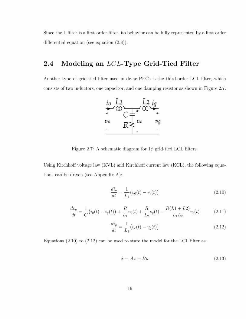
2.7 A schematic diagram for 1φ grid-tied LCL filters. . . . . . . . . . . . . . . 18
3.1 A schematic diagram for grid-connected 1φ VS dc-ac PEC with L filter. . . 25
3.2 Block diagram of the grid-tied 1φ VS dc-ac PEC with L-type filter con-
trolled by a dead-beat controller. . . . . . . . . . . . . . . . . . . . . . . . 26
3.3 Block diagram of the grid-tied 1φ VS dc-ac PEC with L-type filter con-
trolled by a dead-beat controller with observed current feedback. . . . . . . 27
3.4 Block diagram of the grid-tied 1φ dc-ac PEC with L-type filter controlled
by the proposed dead-beat controller with a disturbance estimator. . . . . 29
3.5 Pole locations of the closed-loop transfer function of the disturbance esti-
mator for L filter. . . . . . . . . . . . . . . . . . . . . . . . . . . . . . . . . 32
xi
3.6 Step response of the disturbance estimator for L filter. . . . . . . . . . . . 33
3.7 The response of the closed-loop transfer function to a step change in the
command current: (a) Td = 0, and (b) Td = T . . . . . . . . . . . . . . . . . 35
3.8 The frequency response of the closed-loop transfer function to the command
current: (a) Td = 0, and (b) Td = T . . . . . . . . . . . . . . . . . . . . . . . 36
3.9 The step response of the closed-loop transfer function for several mismatch
ratio κL: (a) Td = 0, and (b) Td = T . . . . . . . . . . . . . . . . . . . . . . 37
3.10 Root locus of the closed-loop transfer function of the grid-tied 1φ dc-ac
PEC with L-type filter for Td = 0. . . . . . . . . . . . . . . . . . . . . . . . 38
3.11 Root locus of the closed-loop transfer function of the grid-tied 1φ dc-ac
PEC with L-type filter for Td = T . . . . . . . . . . . . . . . . . . . . . . . 39
3.12 The frequency response of the closed-loop transfer function to the grid
voltage for Td = T . . . . . . . . . . . . . . . . . . . . . . . . . . . . . . . . 40
3.13 The response of the grid current to a step change in the grid voltage. . . . 41
3.14 The frequency response of the closed-loop transfer function to the grid
voltage estimation error. . . . . . . . . . . . . . . . . . . . . . . . . . . . . 42
3.15 A schematic diagram for grid-connected 1φ VS dc-ac PECs with LCL filter. 43
3.16 Block diagram of the grid-tied 1φ VS dc-ac PEC with LCL-type filter
controlled by the proposed controller. . . . . . . . . . . . . . . . . . . . . . 43
3.17 Pole locations of the closed-loop transfer function of the disturbance esti-
mator for LCL filter. . . . . . . . . . . . . . . . . . . . . . . . . . . . . . . 52
3.18 Step response of the disturbance estimator for LCL filter. . . . . . . . . . . 52
3.19 The response of the closed-loop transfer function to a step change in the
command current with LCL filter. . . . . . . . . . . . . . . . . . . . . . . . 55
3.20 The frequency response of the closed-loop transfer function to the command
current with LCL filter. . . . . . . . . . . . . . . . . . . . . . . . . . . . . . 55
xii

3.21 Root locus of the closed-loop transfer function of the grid-tied 1φ dc-ac
PEC with respect to κL. . . . . . . . . . . . . . . . . . . . . . . . . . . . . 56
3.22 The frequency response of the closed-loop transfer function to the capacitor
current disturbance. . . . . . . . . . . . . . . . . . . . . . . . . . . . . . . . 57
3.23 The frequency response of the closed-loop transfer function to the observed
capacitor current disturbance. . . . . . . . . . . . . . . . . . . . . . . . . . 58
3.24 The frequency response of the closed-loop transfer function to the grid
voltage. . . . . . . . . . . . . . . . . . . . . . . . . . . . . . . . . . . . . . 59
3.25 The frequency response of the closed-loop transfer function to grid voltage
estimation error. . . . . . . . . . . . . . . . . . . . . . . . . . . . . . . . . 60
4.1 A block diagram for the simulation model of the DBCC for an intercon-
nected 1φ VS dc-ac PEC with L-type filter. . . . . . . . . . . . . . . . . . 65
4.2 A block diagram for the bipolar Pulse width modulation (PWM) technique. 66
4.3 Steady-state simulation results with Td = 0.5T and κL = 1. The current
scale is 10 A/div., the voltage scale is 100 V/div., and the disturbance scale
is 10 V/div. Grid voltage of 240 V and command current of 30 A. . . . . . 67
4.4 Steady-state simulation of the observed current and the command current.
The scale is 4 A/div. . . . . . . . . . . . . . . . . . . . . . . . . . . . . . . 67
4.5 Steady-state simulation results with Td = 0.5T and κL = 2. The current
scale is 10 A/div., the voltage scale is 100 V/div., and the disturbance scale
is 10 V/div. Grid voltage of 240 V and command current of 30 A. . . . . . 68
4.6 Steady-state simulation results with Td = 0.5T and κL = 4. The current
scale is 10 A/div., the voltage scale is 100 V/div., and the disturbance scale
is 20 V/div. Grid voltage of 240 V and command current of 30 A. . . . . . 69
xiii

4.7 Steady-state simulation results with Td = 0.5T and κL = 0.5. The current
scale is 10 A/div., the voltage scale is 100 V/div., and the disturbance scale
is 20 V/div. Grid voltage of 240 V and command current of 30 A. . . . . . 69
4.8 Steady-state simulation results with Td = 0.5T , κL = 1, low-order harmon-
ics (3rd = 24 V, 5th = 4.8 V, 7th = 7.2 V, and 9th = 2.4 V) injected to
the grid voltage. The current scale is 10 A/div., the voltage scale is 100
V/div., and the disturbance scale is 10 V/div. Grid voltage of 240 V and
command current of 30 A. . . . . . . . . . . . . . . . . . . . . . . . . . . . 71
4.9 Steady-state simulation results with Td = 0.5T , κL = 1, 10% second order
ripple injected to the dc voltage. The current scale is 10 A/div., the voltage
scale is 40 V/div., and the disturbance scale is 100 V/div. DC voltage of
400 V and command current of 30 A. . . . . . . . . . . . . . . . . . . . . . 72
4.10 Dynamic simulation results to step up/down (0 A to 40 A) with Td = 0.5T
and κL = 1. The current scale is 10 A/div., the disturbance scale is 60
V/div., and the zoomed-in time scale is 1 msec./div. . . . . . . . . . . . . 73
4.11 Dynamic simulation results to step up/down (20 A to 40 A) with Td = 0.5T
and κL = 1. The current scale is 10 A/div., the disturbance scale is 60
V/div., and the zoomed-in time scale is 1 msec./div. . . . . . . . . . . . . 73
4.12 A block diagram for the simulation model of the DBCC for an intercon-
nected 1φ VS dc-ac PEC with an LCL-type filter. . . . . . . . . . . . . . . 75
4.13 Steady-state simulation results with Td = T and κL = 1 . The current scale
is 10 A/div., the voltage scale is 100 V/div., and the disturbance scale is
10 V/div. . . . . . . . . . . . . . . . . . . . . . . . . . . . . . . . . . . . . 76
4.14 Steady-state simulation results with Td = T and κL = 0.75 . The current
scale is 10 A/div., the voltage scale is 100 V/div., and the disturbance scale
is 10 V/div. . . . . . . . . . . . . . . . . . . . . . . . . . . . . . . . . . . . 77
xiv
4.15 Steady-state simulation results with Td = T and κL = 1.5 . The current
scale is 10 A/div., the voltage scale is 100 V/div., and the disturbance scale
is 10 V/div. . . . . . . . . . . . . . . . . . . . . . . . . . . . . . . . . . . . 77
4.16 Steady-state simulation results with Td = T , κL = 1, and low order har-
monics (3rd = 24 V, 5th = 4.8 V, 7th = 7.2 V, and 9th = 2.4 V) injected
to the grid voltage. The current scale is 10 A/div., the voltage scale is 100
V/div., and the disturbance scale is 10 V/div. . . . . . . . . . . . . . . . . 79
4.17 Dynamic simulation results to step up/down (0 A to 40 A) with Td = T
and κL = 1. The current scale is 10 A/div., the disturbance scale is 20
V/div., and the zoomed-in time scale is 2 msec./div. . . . . . . . . . . . . 80
4.18 Dynamic simulation results to step up/down (20 A to 40 A) with Td = T
and κL = 1. The current scale is 10 A/div., the disturbance scale is 20
V/div., and the zoomed-in time scale is 2 msec./div. . . . . . . . . . . . . 80
4.19 Simulation steady-state error comparison of the 1φ dc-ac PEC, with L-
type filter, when controlled by the proposed dead-beat current controller
(DBCC), predictive controller with delay compensator (PCDC), and tra-
ditional predictive controller (TPC) with respect to the model mismatch
ratio κL. . . . . . . . . . . . . . . . . . . . . . . . . . . . . . . . . . . . . . 82
5.1 A photograph of the experimental setup for testing the DBCC. . . . . . . . 85
5.2 Steady-state experimental results of the 10 kW system operated by the
proposed DBCC: the grid current Ig, the grid voltage Vg, and the dc voltage
Vdc. The current scale is 20 A/division, voltage scale is 50 V/division, and
time scale is 4 msec./division . . . . . . . . . . . . . . . . . . . . . . . . . 87
xv

5.3 The dynamic response of the 10 kW system operated by the DBCC: the
grid current Ig and the grid voltage Vg. The current scale is 20 A/division,
voltage scale is 100 V/division, and time scale is 0.1 sec./division. . . . . . 88
5.4 The dynamic response to step up change in the command power from 0.0
kW to 9.6 kW of the grid current Ig and the grid voltage Vg for the 10
kW system when operated by the proposed DBCC. The current scale is 20
A/division, voltage scale is 100 V/division, time scale is 5 msec./division. . 89
5.5 The dynamic response to step down change in the command power from
9.6 kW to 0.0 kW of the grid current Ig and the grid voltage Vg for the 10
kW system when operated by the proposed DBCC. The current scale is 20
A/division, voltage scale is 100 V/division, time scale is 5 msec./division. . 89
5.6 Photograph of the test 10 kW PEC with the inductor bank used for pa-
rameter variation experiment of the L and LCL filters. . . . . . . . . . . . 90
5.7 Grid voltage disturbance experiment setup. . . . . . . . . . . . . . . . . . . 92
5.8 Experimental results of the 10 kW system operated by the DBCC: the grid
voltage Vg and the grid current Ig under grid voltage disturbance. The
current scale is 20 A/division, voltage scale is 100 V/division, and time
scale is 4 msec./division. . . . . . . . . . . . . . . . . . . . . . . . . . . . . 93
5.9 Screen shot of the THD measurements for the grid voltage Vg captured
from HIOKI PW3198 Power Quality Analyzer. . . . . . . . . . . . . . . . . 94
5.10 Screen shot of the THD measurements for the grid current Ig captured
from HIOKI PW3198 Power Quality Analyzer. . . . . . . . . . . . . . . . . 94
5.11 Performance of the 10 kW system operated by the DBCC under grid voltage
disturbance for P ∗g = 9.6 kW and Q∗
g = 0. . . . . . . . . . . . . . . . . . . . 95
5.12 The grid current harmonic components for the case of I∗g(1) = 30 A and
I∗g(3) = 7 A captured from HIOKI PW3198 Power Quality Analyzer. . . . . 96
xvi
5.13 The grid current harmonic components for the case of I∗g(1) = 30 A and
I∗g(5) = 5 A captured from HIOKI PW3198 Power Quality Analyzer. . . . . 98
5.14 A schematic diagram for the setup to test harmonic compensation and
power factor correction. . . . . . . . . . . . . . . . . . . . . . . . . . . . . . 99
5.15 The waveforms of the injected current I and the grid voltage Vg without
harmonic compensation. The current scale is 15 A/division, voltage scale
is 50 V/division, and time scale is 5 msec./division. . . . . . . . . . . . . . 100
5.16 The waveforms of the injected current I and the grid voltage Vg with har-
monic compensation. The current scale is 15 A/division, voltage scale is
50 V/division, and time scale is 5 msec./division. . . . . . . . . . . . . . . 101
5.17 Phasor diagram of the grid current (I1) and grid voltage (U1) for (a)
θ∗i = +45o and (b) θ∗i = −45o. . . . . . . . . . . . . . . . . . . . . . . . . . 103
5.18 Phasor diagram of the total grid current (I = I1) and grid voltage (Vg =
U1) (a) without power factor compensation and (b) with power factor
compensation. . . . . . . . . . . . . . . . . . . . . . . . . . . . . . . . . . . 104
5.19 The experimental results of the developed current controller: the injected
current into the grid Ig, and grid voltage Vg. The current scale is 50 A/di-
vision, voltage scale is 200 V/division, and time scale is 5 µsec/division. . . 106
5.20 The injected current into the grid Ig, and grid voltage Vg under a step
change in the command power P ∗g . The current scale is 50 A/division,
voltage scale is 200 V/division, and time scale is 25 µsec/division for the
upper window and 5 µsec/division for the lower window. . . . . . . . . . . 107
5.21 The injected current into the grid Ig, and grid voltage Vg under a step
change in the command power. The current scale is 50 A/division, voltage
scale is 200 V/division, and time scale is 25 µsec/division for the upper
window and 5 µsec/division for the lower window. . . . . . . . . . . . . . . 108
xvii

1 A schematic diagram for grid-connected 1φ VS dc-ac PECs with LCL filter. 134
2 Block diagram for the simulation model of the TPC for grid-tied 1φ dc-ac
PEC with L-type filter. . . . . . . . . . . . . . . . . . . . . . . . . . . . . . 146
3 Block diagram for the simulation model of the PCDC for grid-tied 1φ dc-ac
PEC with L-type filter. . . . . . . . . . . . . . . . . . . . . . . . . . . . . . 147
4 The digital signal processing board used in this thesis. . . . . . . . . . . . 148
xviii

List of Abbreviations
1φ Single Phase
3φ Three Phase
DGU Distributed Generation Unit
PEC Power Electronic Converter
PI Proportional Integral
FL Fuzzy Logic
ANN Artificial Neural Network
RR Recursive Repetitive
PR Proportional Resonant
PC Predictive Current Controller
VSI Voltage Source Inverter
VS Voltage Source
ADC Analog to Digital Converter
xix

FPGA Field-Programmable Gate Array
DSP Digital Signal Processor
EMI Electromagnetic Interference
KVL Kirchhoff Voltage Law
KCL Kirchhoff Current Law
DBCC Dead-Beat Current Controller
PCDC Predictive Current Controller with Delay Compensator
TPC Traditional Predictive Controller
PWM Pulse Width Modulation
RMSE Root Mean Square Error
IGBT Insulated-Gate Bipolar Transistors
PF Power Factor
THD Total Harmonic Distortion
PCC Point-of-Common-Coupling
xx

List of Symbols
v0 Instantaneous output voltage
vg Instantaneous grid voltage
vdc Instantaneous dc voltage
V0 Average output voltage
Vg Average grid voltage
vdc Average dc voltage
vc RC branch voltage
vcap Capacitor voltage
T Switching cycle
Td Controller time delay
m Modulation index
L Filter inductance
C Filter capacitance
xxi
R Filter resistance
L1 Inverter-side filter inductance
L2 Grid-side filter inductance
Lm Modeled filter inductance
Lm1 Modeled inverter-side filter inductance
Lm2 Modeled grid-side filter inductance
Cm Modeled filter capacitance
Rm Modeled filter resistance
ig Gird current
io Inverter output current
ic Capacitor current
ig Observed gird current
io Observed inverter output current
ic Observed capacitor current
fg Grid frequency
ERMS Relative error
PF Power factor
THD Total harmonic distortion factor
P ∗g Command real power
Q∗g Command reactive power
1
Chapter 1
Introduction
1.1 General
The continuous growth in the global demands for electric energy has initiated different
changes in the operation and control of power systems. Among these changes is the
interconnection of distributed generation units (DGUs). Energy conversion systems fed
by wind, solar, geothermal, and fuel cell sources are widely integrated for electric power
in different countries. The technologies employed in interconnecting DGUs are mainly
composed of power electronic converters (PECs).
One of the major concerns is the power quality, which can be adversely impacted by the
current and/or voltage harmonics produced by PECs used in DGUs. On one hand, since
DGUs are operated in grid-connection, the voltage harmonics are negligible due to the
high quality voltage of the host power system. On the other hand, current harmonics
remain the major concerns for power quality problems on power systems that host DGUs.
In order to minimize the current harmonics, grid-tied filters are used to interconnect the
PECs to the host grid [1–3]. Among the popular grid-tied filters used in the PECs are: L
filters, LC filters, LCL filters [4–9], LLCL filters [10], and LCL-LC filter [11].
2
Along with the type of the grid-tied filter used to interface the PEC to the host grid, the
control of PECs employed in DGUs has a vital importance due to their functions during
the grid-connected operation. As the number of interconnected DGUs has significantly
increased, concerns have been raised on the impacts of DGUs on the operation, control,
and protection of power systems hosting DGUs.
Several controllers have been developed for voltage-source (VS) grid-connected PECs.
Among the widely used controller are the current controllers, which have demonstrated
good abilities to regulate power delivered to the host grid, while complying with the
standards and industrial codes [13–15]. Despite their diverse designs, existing current
controllers have suffered limited capabilities to fully achieve the aforementioned objectives,
due to sensitivity to variations in system or controller parameters. The proportional
integral (PI) [16,18–21], fuzzy logic (FL) [22,23], artificial neural networks (ANN) [24,25],
recursive repetitive (RR) [26–28], proportional resonant (PR) [29, 31–47], and predictive
current controllers (PC) [47–67], have become very popular for operating single-phase
(1φ) VS dc-ac PECs.
1.2 Literature Review
The wide employment of 1φ PECs in different applications has motivated improving their
interface with the host grid, and enhancing their controllers’ performances. The following
subsections overview the different current controllers used for operating 1φ VS dc-ac
PECs in grid-connected mode. Moreover, the following sections provide a summary of
the different filter designs used for interfacing 1φ VS dc-ac PECs with their host grid.
3
1.2.1 Current Controllers for Grid-Connected 1φ VS DC-AC
PECs
The literature reports several designs for current controllers developed for grid-connected
PECs to meet the standard power quality requirements, as well as to facilitate stable
and steady power flow from/to controlled PECs. Among the popular designs are: the
proportional-integral (PI), fuzzy logic (FL), artificial neural networks (ANN), recursive
repetitive (RR), proportional resonant (PR) and predictive current controllers (PC).
The conventional proportional-integral (PI) controllers have shown significant perfor-
mance in three-phase (3φ) PECs as current controllers, due to their design and imple-
mentation using d-q-axis components [19, 20, 68]. However, due to the decomposition of
the ac variables into the d- and q-axis, the control scheme contains double the required
controllers. Moreover, it is difficult to implement such decomposition using low-cost fixed-
point digital signal processing (DSP) [17]. In 1φ PECs, PI current controllers face several
challenges, including reduced accuracy and stability for handling time varying (sinusoidal)
signals, poor disturbance rejection, slow response to abrupt and drastic changes, sensitiv-
ity to changes in system parameters, and complicated tuning for sinusoidal signals [18].
Many modifications have been proposed to the classical PI current controllers to overcome
these challenges such as the addition of grid voltage forward path, multiple state feedback,
and increasing the proportional gain. These modifications can expand the PI controller
bandwidth on the expense of their stability margins [29].
Another modification to the classical PI current controllers has been introduced using
artificial intelligence approaches such as fuzzy-logic (FL) and artificial neural networks
(ANN), where the PI blocks in the controller are replaced by self-tuned PI controllers.
The transient overshoots and the tracking error can be significantly reduced using the
FL self-tuned PI controllers [30]. However, the FL controllers are very sensitive to any
4

change in the fuzzy set shapes and overlapping. On the other hand, ANN controllers are
very sensitive to the operating conditions of the system. For instance, the performance of
these controllers degrades significantly if the system operating point is out of the range
of the trained operating conditions [25].
Recursive repetitive controllers (RR) are based on the internal mode principle where the
internal model of the command current generator is included in the controller transfer
function [68–74]. This approach allows these controllers to achieve zero steady-state error
in tracking sinusoidal command current [75]. However, these controllers introduce several
resonant peaks at multiple frequencies. Additional damping and filtering are required
to minimize these resonant peaks. As a consequence, the steady-state error is increased.
Moreover, the tuning of the controller and the filter coefficients becomes challenging [68].
The proportional-resonant (PR) controllers have been adopted in many power converter
applications such as wind turbines [34–39,47], photovoltaic inverters [40–42,76], and active
power filters [43–46]. The principle of these controllers is based on setting their open-loop
gain to infinity at the resonance frequency so that the closed-loop gain is unity and the
phase shift is zero at the resonance frequency [68]. This feature of PR controllers can offer
an effective elimination of steady-state error. In applications for grid-connected PECs,
the resonance frequency can be selected as the frequency of the host grid to provide
accurate and fast responses [31, 32]. However, the stability margins and the bandwidth
are affected by these controllers. Hence, these controllers need cautious design [33]. In
addition, PR controllers are very sensitivity to variations in system parameters [33, 59].
The PR controllers are designed in the continuous domain, however, they are implemented
digitally. PR controllers are very sensitive to the discretization process [68].
Predictive current controllers have demonstrated several advantages over other current
controllers, mainly for applications in grid-connected PECs. Such advantages include
fast, dynamic, and accurate responses, along with stable digital implementations. How-
5

ever, existing implementations of predictive current controllers suffer from degraded per-
formance due to the time-delay introduced by the system requirements, especially in the
presence of changes in system parameters [48–54]. Several methods have been proposed to
overcome such a limitation and improve the overall performance of predictive current con-
trollers. These methods can be classified based on their objectives, which include reducing
the sensitivity to parameter variations [49–51, 81, 83], rejecting disturbances experienced
by the controlled system [52, 53, 77–79], compensating for the time-delay [54–58, 80–82],
and minimizing the steady-state error [61]. The employment of these methods have im-
proved the performance of current controllers in term of their accuracy and ability to
reject grid side disturbances. Nonetheless, the complex implementation together with
the requirements for additional measurements remain a challenge for the applications of
current controllers in grid-connected PECs. State observers have been proposed [55–57]
as an attempt to reduce the impacts of the delay created by the controller. However,
the inclusion of the state observer can aggravate the controller sensitivity to parameter
variations, thus complicating the response of the controller. In reference [58], an improved
implementation of a digital dead-beat current controller is developed for applications in
interconnected PECs. This implementation is based on minimizing the delay of the con-
troller using high-speed analog-to-digital converters (ADCs) and field-programmable gate
array (FPGA) platform. This improved implementation of the predictive current con-
troller requires complex circuitries that may not be possible using low-cost fixed-point
DSP.
1.2.2 Grid-Tied Filter Design
Grid-tied filters are used to interface a PEC to its host grid. The main assumption for the
grid is that it is an ac source, whose voltage and frequency do not change due to the power
injected by the interfaced PEC. The main function for a grid-tied filter is to block the
6

harmonic components, produced by the PEC, from flowing to the host grid. Moreover,
grid-tied filters have to be able to block grid-side disturbances from affecting the PEC
operation. Among the common grid-tied filter designs reported in the literature are the L,
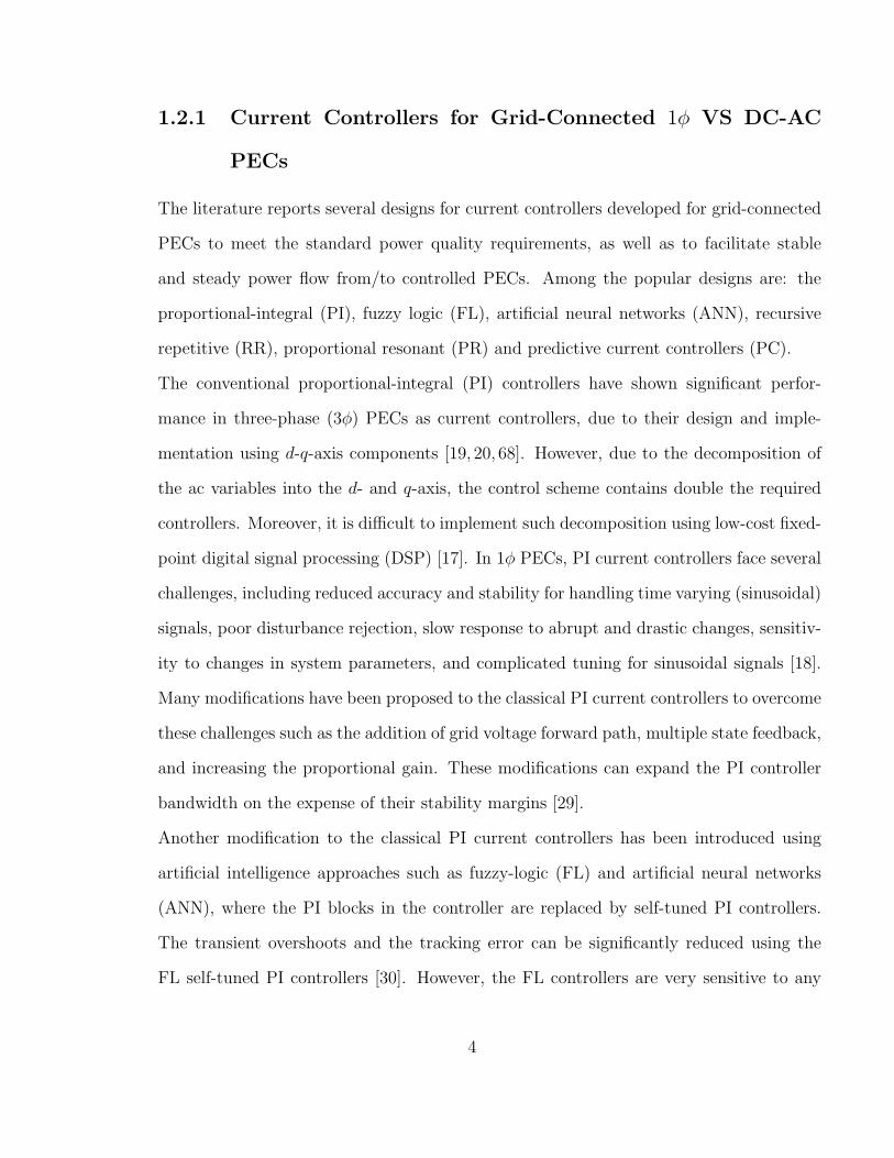
LC, LCL, and LLCL filters. The general configurations of these filters are shown in Figure
1.1. The first order L filters are commonly used in the interconnection of dc-ac PECs to the
host grid due to their simple structure and natural stability. However, these filters require
large inductance to eliminate the high frequency current harmonics, which increases their
cost and size. Several techniques have been used in the industry to overcome these
drawbacks such as operating the dc-ac PECs at higher switching frequency, adopting more
complex topologies and control algorithms, or using higher order grid-tied filters [87–89].
For instance, LC or LCL filters provide higher attenuation than L filters, which results
in reduced size and cost, however, these filters are inherently unstable. Passive or active
damping methods are used for stabilizing these filters [90–96]. Passive damping methods
are based on inserting a damping resistor to the filter to achieve stable operation on the
expenses of higher power loss [93]. Active damping methods do not require any additional
component since they can be achieved by the controller system. However, they require
more sensing elements to measure the feedback variable, they increase the controller
complexity, and they are sensitive to parameter variation [92].
The higher order LLCL filters are based on inserting small inductance in series with the
capacitor of the traditional LCL filter as shown in Figure 1.1 (d). This will result in a series
resonance at the switching frequency which provides better attenuation of the current
ripple components than LCL filters. However, this LC branch causes electromagnetic
interference (EMI) [12]. In addition, these filters are sensitive to the parameters of the
LC branch which may affect the resonant frequency.
The performance of the current controller is significantly affected by the type of filter used
in the interconnection of the dc-ac PECs to the grid. As a consequence, the design and
7
implementation of the current controller must be modified based on the grid-tied filter
used.
Figure 1.1: Common grid-tied filters used in the dc-ac PECs: (a) L filter, (b) LC filter,(c) LCL filter, and (d) LLCL filter.
1.3 Motivation
The traditional power system is changing from the unidirectional power flow to bidirec-
tional power flow. These changes in the power system are in favor of utilizing a mix of
DGUs fed by solar, wind, geothermal, and fuel cell sources. The technology used is these
units are mainly composed of PECs. Due to the nonlinear nature of the PECs, several
concerned have been raised about their impact on the operation, control, and protection
of the host power system. One of the major concern is the harmonic distortion injected
by these PECs and its impact of the power quality of the host power system. In addi-
tion, harmonic distortion is problematic because it causes excessive heating and pulsating
torques in motors and generators, voltage stress across capacitors, misoperation of elec-
8

tronics and relaying, and reduction in life-time of equipment and components. Moreover,
IEEE standard and industrial codes set the limits of the total harmonic distortion of any
grid-connected PECs to less than 5% at full load. Since the PECs are operated in grid-
connection mode, the voltage harmonics are negligible due to the high quality voltage of
the host power system. On the other hand, current harmonics remain the major concerns
for power quality problems on power systems that host PECs. A widely accepted approach
to operate these PECs during grid-connection mode in order to meet the standards and
industrial codes are the utilization of grid current controllers along with grid-tied filters.
The review of the existing current controllers highlights three main challenges: the sensi-
tivity to parameter variation in the system, the sensitivity to the time delay due to the
digital implementation of these controllers, and the sensitivity to grid-side disturbances.
These challenges deteriorate the performance of the PECs in regulating the power flow
while meeting the industrial and standard codes. As the integration of 1φ DGUs such as
small-scale wind turbine, solar systems, battery chargers, and electric vehicle chargers is
expected to increase, the mandate for robust current controllers, for grid-connected 1φ
PECs, is expected to grow. The development of accurate controllers, for grid-connected
1φ PECs, capable of offering accurate, stable, and reliable responses with negligible sen-
sitivity to changes in system parameters and/or the grid voltage disturbances, are the
motivations for this research.
1.4 Objectives
The review of existing current controllers used for grid-connected PECs highlight three
main challenges that are the digital implementation (the delay of the controller), the
sensitivity to changes in the system parameters, and the grid voltage disturbance. The
research of this thesis aims to provide solutions for the aforementioned issues. The research
9

objectives of this thesis can be stated as:
• to analyze, design, develop, and test a robust current controller for applications
in grid-connected single-phase VS dc-ac PECs. The proposed current controllers
are designed as a digital dead-beat controller with a disturbance estimator, which
can accurately regulate the power delivery to the grid, and can ensure meeting the
standards for grid-connection.
• to achieve accurate, stable, and reliable responses with negligible sensitivity to the
controller time delay, changes in system parameters, and grid voltage disturbance.
• to adopt the proposed controller to operate a dc-ac PEC with first order grid-tied
L filter as well as with the third order grid-tied LCL filter.
1.5 Thesis Outline
This Ph.D. dissertation contains six chapters including this introductory chapter. The
remainder of this dissertation is arranged as follows.
• Chapter 2 presents the model of a grid-connected 1φ VS dc-ac PEC. The continuous
models of 1φ VS dc-ac PEC with L filter and LCL filter are given first. Then, the
discrete models are driven using zero-order-hold and z-transform techniques.
• Chapter 3 discusses the development and design of the proposed controllers with the
disturbance estimator. In addition, the stability and performance of the proposed
controllers are investigated using the pole location, step response, and frequency
response.
• Chapter 4 and Chapter 5 show the simulation and experimental results of the pro-
posed controllers. The steady-state response under time delay, parameter variation,
10

and grid voltage disturbances are evaluated. Moreover, the dynamic response to
step changes in the command power is also presented.
• Chapter 6 discusses the contribution of the thesis, and suggests avenues for future
research.
11

Chapter 2
Steady-State Analysis of a
Single-Phase Grid-Connected VS
DC-AC PEC
2.1 General
The latest trends in power system operation have been in favor of utilizing a mix of
generating units. Such a mix is made up of conventional synchronous generators and
distributed generation units (DGUs). There are various types of DGUs, including co-
generation units, wind energy systems, solar energy systems, ocean generation units, and
others. Nowadays, some countries have up to 40% of their total electricity generated by
combinations of different DGUs (e.g. wind, solar, geothermal, etc.). Figure 2.1 shows a
portion of a power system that integrates several types of DGUs.
Since the majority of existing DGUs have renewable energies as their inputs, their out-
put electric power has an intermittent nature, which prevents the direct interconnection
with power systems. In order to overcome this technical difficulty, PECs are employed in
12

different types of DGUs. Single-phase and three-phase ac-dc, dc-ac, and dc-dc PECs are
widely employed in wind, solar, tidal, ocean, and fuel cells systems. Despite their remark-
able performance, the non-linear and switched inherent natures of PECs, employed in
DGUs, have raised several concerns regarding power quality, voltage/frequency stability,
and impacts on protection devices. The literature reports different approaches that have
been developed to address such concerns. The majority of these approaches are based on
improving the control of front-end PECs, which are used to interface DGUs with a power
system or an isolated load.
Single-phase dc-ac PECs are among the topologies used to interface DGUs to power
systems. These PECs have some operational, maintenance, and economic advantages
that can be suitable for low power rated DGUs. Despite such advantages, 1φ dc-ac PECs
require accurate, reliable, and robust controllers to ensure meeting their objectives. The
initial stage of designing a controller with the previous features mandates developing a
model for a grid-connected 1φ dc-ac PEC. This chapter presents and discusses the steady-
state modeling and analysis of a 1φ VS grid-connected dc-ac PEC. The steady-state model
in this chapter is developed with the following assumptions:
• The switching cycle T is a time-invariant parameter;
• In each T , only two switching elements change their conduction states;
• The input dc voltage vdc is a slow time-varying signal with respect to the switching
cycle T ;
• Parameters of the grid-tied filter (L, C, and/or R) are constants over each T ;
• The modulation index m (with m ∈ [−1, 1]) is updated once every T .
13

Figure 2.1: The integration of DGUs in a power system.
2.2 Modeling a 1φ VS DC-AC PEC
The 1φ VS dc-ac PEC consists of 4 switching elements, S1, S2, S3, and S4, which are con-
figured as an H-bridge as depicted in Figure 2.2. The instantaneous output voltage, vo(t),
is dependent on the instantaneous dc input voltage, vdc(t), and on the active switching
elements in the 1φ dc-ac PEC. In general, there are four valid states of operations, based
on the conduction state of each switching elements. These four states are illustrated in
Figure 2.3.
14
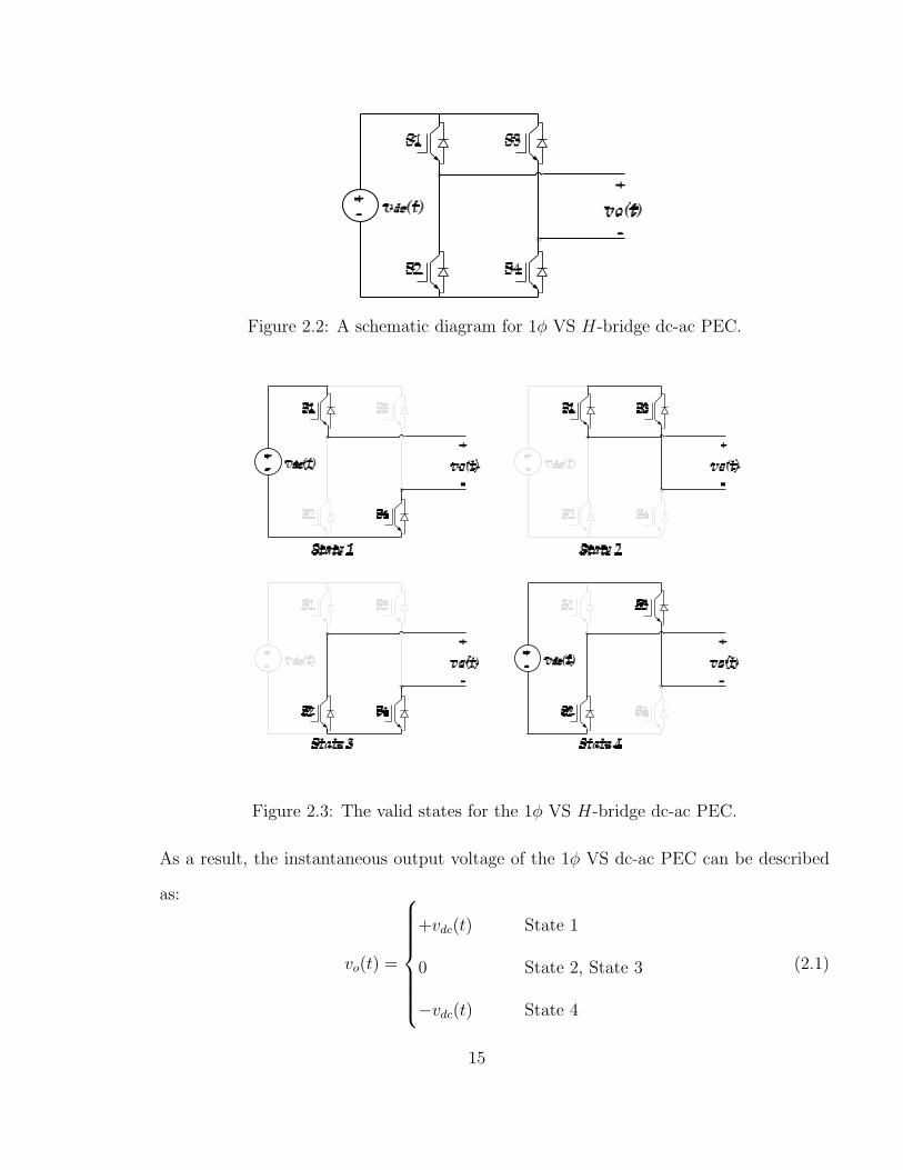
Figure 2.2: A schematic diagram for 1φ VS H-bridge dc-ac PEC.
Figure 2.3: The valid states for the 1φ VS H-bridge dc-ac PEC.
As a result, the instantaneous output voltage of the 1φ VS dc-ac PEC can be described
as:
vo(t) =
+vdc(t) State 1
0 State 2, State 3
−vdc(t) State 4
(2.1)
15
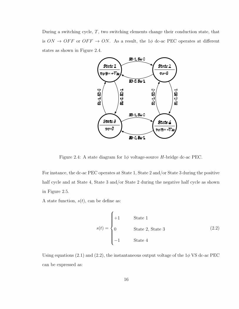
During a switching cycle, T , two switching elements change their conduction state, that
is ON → OFF or OFF → ON . As a result, the 1φ dc-ac PEC operates at different
states as shown in Figure 2.4.
Figure 2.4: A state diagram for 1φ voltage-source H-bridge dc-ac PEC.
For instance, the dc-ac PEC operates at State 1, State 2 and/or State 3 during the positive
half cycle and at State 4, State 3 and/or State 2 during the negative half cycle as shown
in Figure 2.5.
A state function, s(t), can be define as:
s(t) =
+1 State 1
0 State 2, State 3
−1 State 4
(2.2)
Using equations (2.1) and (2.2), the instantaneous output voltage of the 1φ VS dc-ac PEC
can be expressed as:
16

Time (msec)0 2 4 6 8 10 12 14 16
Voltage
(V)
-vdc(t)
0
+vdc(t)
vo(t)
vg(t)
Figure 2.5: Waveforms of the output voltage vo(t) and the grid voltage vg(t).
vo(t) = s(t)vdc(t) (2.3)
The average output voltage over T can be obtained as follows:
Vo =1
T
∫ t0+T
t0
vo(t)dt
=1
T
∫ t0+T
t0
s(t)vdc(t)dt
(2.4)
It should be noted that the dc voltage, vdc(t), is a relatively slow time-varying signal with
respect to the switching period T , hence it can be assumed constant during T , that is
vdc(t) = Vdc. This assumption leads to rewriting equation (2.4) as:
Vo = Vdc
1
T
∫ t0+T
t0
s(t)dt (2.5)
17

The modulation index, m, can be defined as the average of the state function over T as:
m(t) =1
T
∫ t0+T
t0
s(t)dt (2.6)
The expression in equation (2.6) allows stating the average output voltage over T as:
Vo = mVdc; m ∈ [−1, 1] (2.7)
2.3 Modeling an L-Type Grid-Tied Filter
The simplest type of grid-tied filter used in dc-ac PECs is the L filter, which consists of
one series inductor as shown in Figure 2.6.
Figure 2.6: A schematic diagram for 1φ grid-tied L filters.
The relationship between the input voltage of the filter, v0(t), and the grid voltage, vg(t),
is given by:
digdt
=1
L
(v0(t)− vg(t)
)(2.8)
Equation (2.8) has the following solution that models the current injected to the host
grid:
ig(t) = ig(t0) +1
L
∫ t
t0
(v0(τ)− vg(τ))dτ (2.9)
18
Since the L filter is a first-order filter, its behavior can be fully represented by a first order
differential equation (see equation (2.8)).
2.4 Modeling an LCL-Type Grid-Tied Filter
Another type of grid-tied filter used in dc-ac PECs is the third-order LCL filter, which
consists of two inductors, one capacitor, and one damping resistor as shown in Figure 2.7.
Figure 2.7: A schematic diagram for 1φ grid-tied LCL filters.
Using Kirchhoff voltage law (KVL) and Kirchhoff current law (KCL), the following equa-
tions can be driven (see Appendix A):
diodt
=1
L1
(v0(t)− vc(t)
)(2.10)
dvcdt
=1
C
(i0(t)− ig(t)
)+
R
L1
v0(t) +R
L2
vg(t)−R(L1 + L2)
L1L2
vc(t) (2.11)
digdt
=1
L2
(vc(t)− vg(t)
)(2.12)
Equations (2.10) to (2.12) can be used to state the model for the LCL filter as:
x = Ax+ Bu (2.13)
19
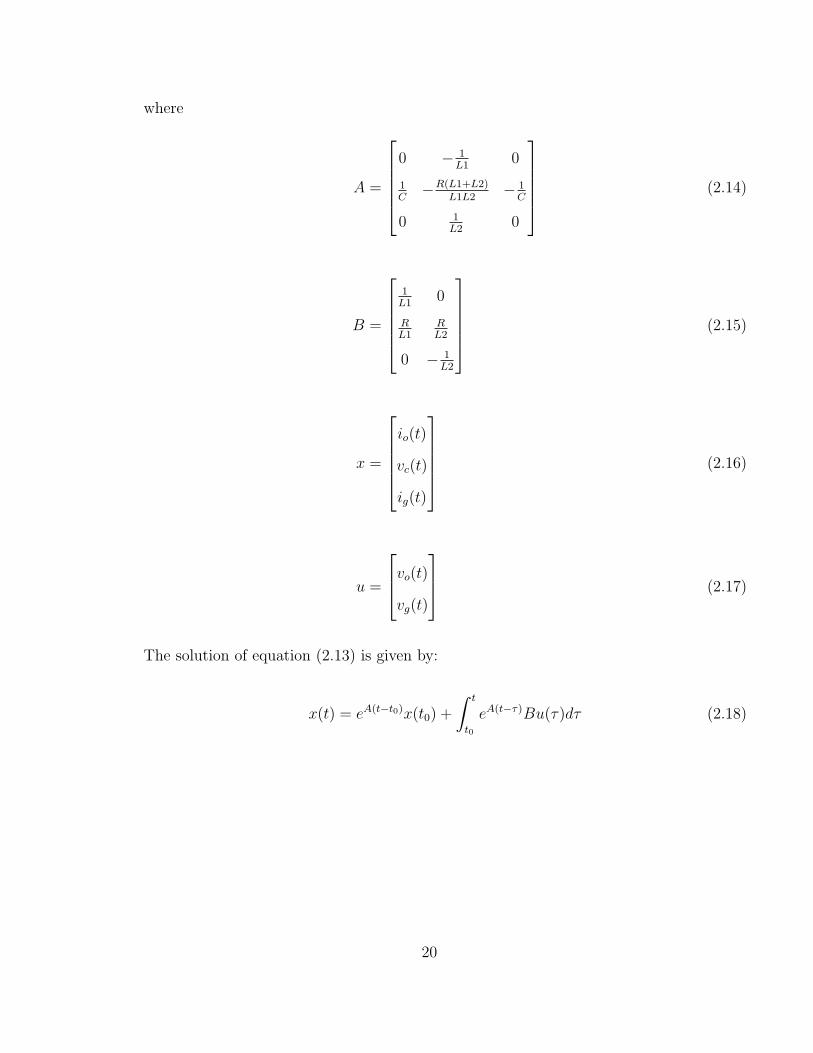
where
A =
0 − 1L1
0
1C
−R(L1+L2)L1L2
− 1C
0 1L2
0
(2.14)
B =
1L1
0
RL1
RL2
0 − 1L2
(2.15)
x =
io(t)
vc(t)
ig(t)
(2.16)
u =
vo(t)
vg(t)
(2.17)
The solution of equation (2.13) is given by:
x(t) = eA(t−t0)x(t0) +
∫ t
t0
eA(t−τ)Bu(τ)dτ (2.18)
20
2.5 Modeling a Grid-Connected 1φ VS H-bridge DC-
AC PEC
Digital controllers have become more popular in the industry due to their advantages
such as easy implementation of more functional control schemes and flexibility. There
are two methods to implement a digital controller [84]. The first method is to design
the controller in the continuous-time domain and then digitize it using discretization
techniques. In this method, the effect of sample and hold process is not considered.
Moreover, the designed controller is sensitive to the discretization technique used. The
second method is based on converting the continuous model to a discrete model and
designing its controller in the digital domain. In the second method, the effect of sample
and hold process is considered which results in a better transient response. In this thesis,
the second approach is employed for designing the proposed current controller. In the
next sections, the discrete models of the grid-connected 1φ VS dc-ac PECs with L filter
as well as LCL filter are given.
2.5.1 Discrete Modeling of a 1φ VS H-bridge DC-AC PEC with
an L-Type Filter
Equation (2.9) can be discretizate over the period T by substituting t0 = kT and t =
(k + 1)T , that is:
ig(k + 1) = ig(k) +1
L
∫ (k+1)T
kT
(v0(τ)− vg(τ))dτ (2.19)
Substituting equation (2.3) into (2.19) yields to:
ig(k + 1) = ig(k) +1
L
∫ (k+1)T
kT
(s(τ)vdc(τ)− vg(τ))dτ (2.20)
21
Using the assumptions in section 2.1, where vdc(t) = Vdc is a constant, equation (2.20)
can be simplified as:
ig(k + 1) = ig(k) +1
L
(Vdc
∫ (k+1)T
kT
s(τ)dτ −∫ (k+1)T
kT
vg(τ)dτ
)(2.21)
Using equation (2.6), (2.21) can be simplified to:
ig(k + 1) = ig(k) +T
L(m(k)Vdc − Vg(k)) (2.22)
where Vg(k) is the average grid voltage over the period [kT, (k + 1)T ]. Applying the
z-transform to equation (2.22) yields to a transfer function for a 1φ VS H-bridge dc-ac
PEC, which is grid-connected through an L-type filter as:
Ig(z) =T
L
1
z − 1(m(z)Vdc − Vg(z)) (2.23)
2.5.2 Discrete Modeling of a 1φ VS H-bridge DC-AC PEC with
an LCL-Type Filter
The discrete model for a 1φ VS H-bridge dc-ac PEC, which is grid-connected through an
LCL-type filter can be derived by substituting t0 = kT and t = (k + 1)T into (2.18) as:
x(k + 1) = eATx(k) +
∫ (k+1)T
kT
eA((k+1)T−τ)Bu(τ)dτ (2.24)
Equation (2.24) can be simplified by averaging u(τ) over the period [kT, (k + 1)T ] as:
x(k + 1) = eATx(k) + U(k)
∫ (k+1)T
kT
eA((k+1)T−τ)Bdτ (2.25)
22
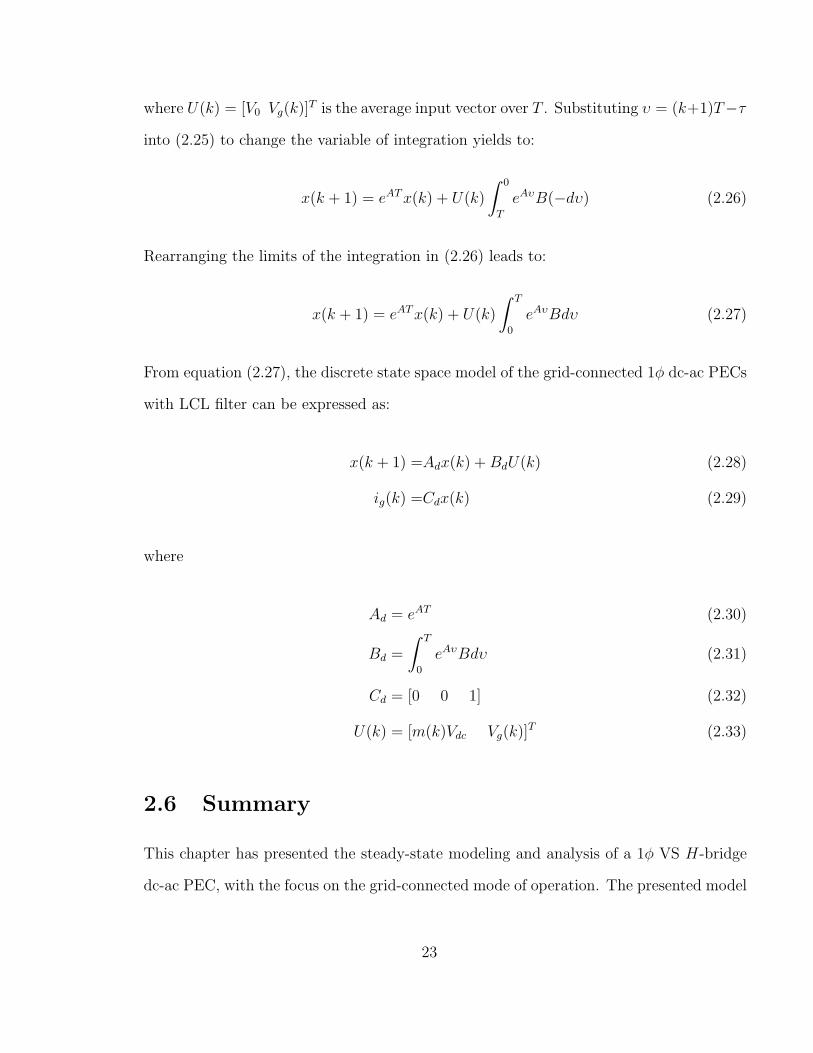
where U(k) = [V0 Vg(k)]T is the average input vector over T . Substituting υ = (k+1)T−τ
into (2.25) to change the variable of integration yields to:
x(k + 1) = eATx(k) + U(k)
∫ 0
T
eAυB(−dυ) (2.26)
Rearranging the limits of the integration in (2.26) leads to:
x(k + 1) = eATx(k) + U(k)
∫ T
0
eAυBdυ (2.27)
From equation (2.27), the discrete state space model of the grid-connected 1φ dc-ac PECs
with LCL filter can be expressed as:
x(k + 1) =Adx(k) + BdU(k) (2.28)
ig(k) =Cdx(k) (2.29)
where
Ad = eAT (2.30)
Bd =
∫ T
0
eAυBdυ (2.31)
Cd = [0 0 1] (2.32)
U(k) = [m(k)Vdc Vg(k)]T (2.33)
2.6 Summary
This chapter has presented the steady-state modeling and analysis of a 1φ VS H-bridge
dc-ac PEC, with the focus on the grid-connected mode of operation. The presented model
23

has been developed based on widely used assumptions, which allow the utilization of the
switching averaged approach for steady-state modeling. As the focus of this thesis is on
the grid-connected mode, this chapter has also presented steady-state models for common
designs of the grid-tied filters, particularly the L-type and LCL-type. The developed
models of the 1φ VS H-bridge dc-ac PEC and grid-tied filters have been discretized for
purposes of designing and implementing digital controllers. In the following chapter,
the obtained discrete models will be employed in designing and implementing current
controllers for operating a 1φ VS H-bridge dc-ac PEC in the grid-connected mode, and
ensuring its stable functions under different conditions.
24
Chapter 3
Current Control of a Grid-Connected
Single-Phase Voltage-Source DC-AC
Power Electronic Converter
3.1 Background
One of the key requirements for ensuring a stable operation of grid-connected PECs, is an
accurate and robust control. In case of 1φ VS dc-ac PECs, the literature reports several
designs of such controllers. As was discussed in Chapter 1, the design of existing controllers
is mostly set as current controllers, which include the conventional proportional-integral,
fuzzy logic, artificial neural networks, recursive repetitive, proportional resonant, and
predictive current controllers. In general, existing current controllers for grid-connected
PECs have shown limited performance due to the sensitivity to parameter variations,
time delay due to the digital implementation, and reduced capabilities to handle grid
disturbances. If a current controller can be designed to overcome such limitations, it will
improve the functionality, stability, and overall efficiency of grid-connected 1φ VS dc-ac
25
PECs. This chapter presents and discusses the design and implementation of a dead-beat
current controller (DBCC) for grid-connected 1φ VS dc-ac PECs, which have either an
L-type or an LCL-type grid-tied filters. The requirements for the designed DBCC are set
for accurate regulation of the power delivery to the grid, while meeting the standards and
codes for grid-connection. Meeting these requirements is to be achieved with negligible
sensitivity to the controller time delay, variations in system parameters, and high ability
to handle grid disturbances.
3.2 Dead-Beat Current Controller for a Grid-
Connected 1φ VS DC-AC PEC with L-Type Fil-
ter
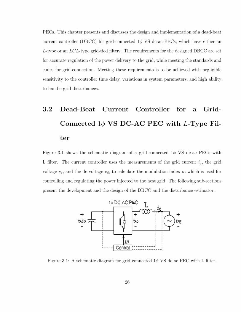
Figure 3.1 shows the schematic diagram of a grid-connected 1φ VS dc-ac PECs with
L filter. The current controller uses the measurements of the grid current ig, the grid
voltage vg, and the dc voltage vdc to calculate the modulation index m which is used for
controlling and regulating the power injected to the host grid. The following sub-sections
present the development and the design of the DBCC and the disturbance estimator.
Figure 3.1: A schematic diagram for grid-connected 1φ VS dc-ac PEC with L filter.
26
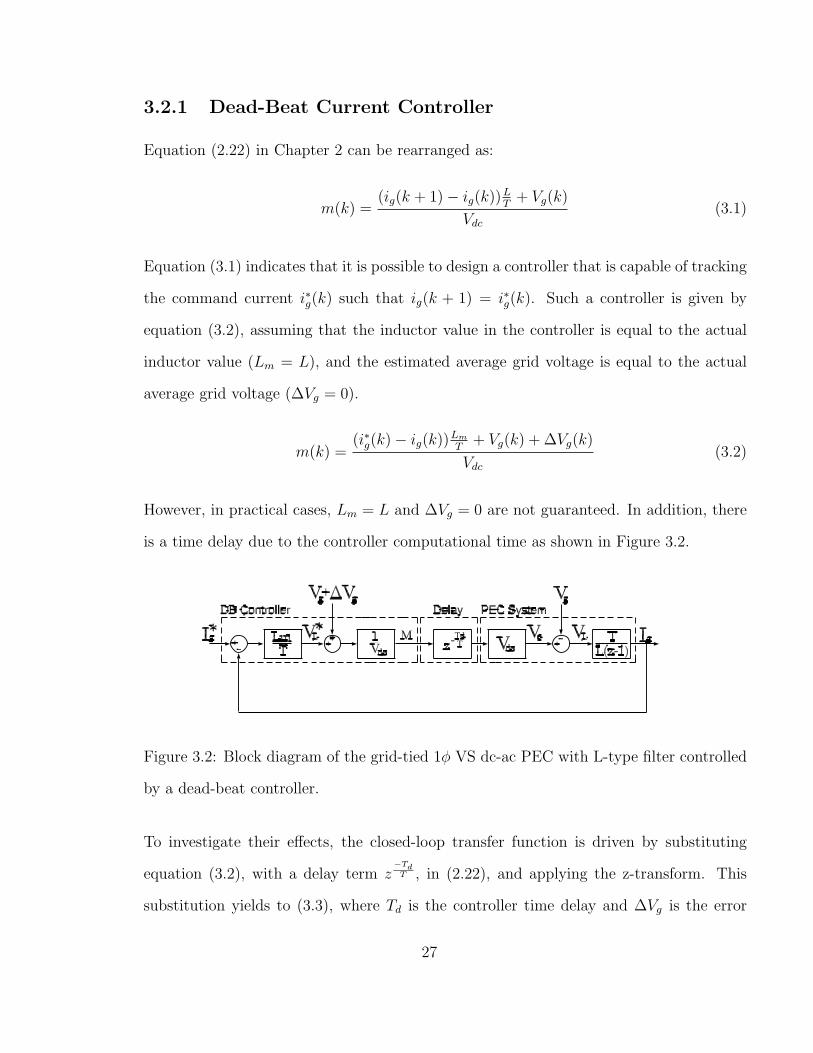
3.2.1 Dead-Beat Current Controller
Equation (2.22) in Chapter 2 can be rearranged as:
m(k) =(ig(k + 1)− ig(k))
LT+ Vg(k)
Vdc
(3.1)
Equation (3.1) indicates that it is possible to design a controller that is capable of tracking
the command current i∗g(k) such that ig(k + 1) = i∗g(k). Such a controller is given by
equation (3.2), assuming that the inductor value in the controller is equal to the actual
inductor value (Lm = L), and the estimated average grid voltage is equal to the actual
average grid voltage (∆Vg = 0).
m(k) =(i∗g(k)− ig(k))
Lm
T+ Vg(k) + ∆Vg(k)
Vdc
(3.2)
However, in practical cases, Lm = L and ∆Vg = 0 are not guaranteed. In addition, there
is a time delay due to the controller computational time as shown in Figure 3.2.
Figure 3.2: Block diagram of the grid-tied 1φ VS dc-ac PEC with L-type filter controlled
by a dead-beat controller.
To investigate their effects, the closed-loop transfer function is driven by substituting
equation (3.2), with a delay term z−Td
T , in (2.22), and applying the z-transform. This
substitution yields to (3.3), where Td is the controller time delay and ∆Vg is the error
27

between the actual average grid voltage and the estimated average grid voltage during
the interval [k, k + 1]. Equation (3.3) indicates that the locations of the poles of the
closed-loop system depend on the ratio Lm/L.
Ig =Lm
Lz
−Td
T
z − 1 + Lm
Lz
−Td
T
· I∗g +TL(z
−Td
T − 1)
z − 1 + Lm
Lz
−Td
T
· Vg +TLz
−Td
T
z − 1 + Lm
Lz
−Td
T
·∆Vg (3.3)
In order to ensure that the pole locations are independent of the ratio Lm/L, the feedback
signal is changed from the current Ig to the observed current Ig as illustrated in Figure
3.3.
Figure 3.3: Block diagram of the grid-tied 1φ VS dc-ac PEC with L-type filter controlled
by a dead-beat controller with observed current feedback.
The observer H(z), given in equation (3.4), models the grid-connected 1φ VS dc-ac PEC
with L filter, as derived in Chapter 2. The expression for H(z) is stated as:
H(z) =T
Lm
1
z − 1(3.4)
The inclusion of the observed current feedback changes equation (3.3) to:
Ig =Lm
Lz
−Td
T
z· I∗g +
TL(z
−Td
T − 1)
z − 1· Vg +
TLz
−Td
T
z − 1·∆Vg
(3.5)
By changing the feedback signal from Ig to Ig, the feedback path becomes independent
28

of L and Td. However, the grid current Ig cannot track the command current I∗g in
steady-state due to the disturbances resulting from the model mismatch (when Lm 6= L),
time delay (when Td 6= 0), and grid voltage measurements error (when ∆Vg 6= 0). This
leads to inaccurate regulation of the power delivery to the grid. A disturbance estimator
is needed in order to compensate these disturbances so that the grid current Ig tracks
the command current I∗g in steady-state with negligible sensitivity to the variations of
system parameters, controller time delay, and ability to handle grid disturbances. Unlike
the other compensation techniques, the disturbance estimator technique in this thesis is
independent of the system parameters and controller time delay.
3.2.2 Disturbance Estimator
Equation (3.5) can be re-arranged in order to separate the desired response from the
disturbance as:
Ig = I∗g · z−1 +T
L
z−Td
T
z − 1·D (3.6)
where D is the disturbance affecting the system (see equation (3.7)). The disturbance D
consists of three terms, the model mismatch disturbance (when Lm 6= L), the time delay
disturbance (when Td 6= 0) , and the grid voltage disturbance (when ∆Vg 6= 0), and can
be expressed as (see Appendix A):
D(z) = I∗g ·z − 1
z
(Lm − L)
T+
(I∗g ·
z − 1
z
L
T+ Vg
)(1− 1
z−Td
T
) + ∆Vg (3.7)
An estimator is used to compensate for the effect of D by estimating the required com-
pensation D such that the controller achieves deadbeat response, as shown in Figure
3.4.
29
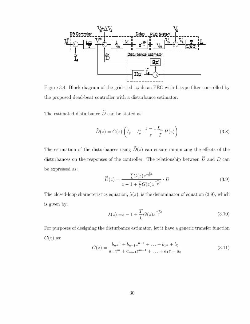
Figure 3.4: Block diagram of the grid-tied 1φ dc-ac PEC with L-type filter controlled by
the proposed dead-beat controller with a disturbance estimator.
The estimated disturbance D can be stated as:
D(z) = G(z)
(Ig − I∗g ·
z − 1
z
Lm
TH(z)
)(3.8)
The estimation of the disturbances using D(z) can ensure minimizing the effects of the
disturbances on the responses of the controller. The relationship between D and D can
be expressed as:
D(z) =TLG(z)z
−Td
T
z − 1 + TLG(z)z
−Td
T
·D (3.9)
The closed-loop characteristics equation, λ(z), is the denominator of equation (3.9), which
is given by:
λ(z) =z − 1 +T
LG(z)z
−Td
T (3.10)
For purposes of designing the disturbance estimator, let it have a generic transfer function
G(z) as:
G(z) =bnz
n + bn−1zn−1 + . . .+ b1z + b0
amzm + am−1zm−1 + . . .+ a1z + a0(3.11)
30

Substituting equation (3.11) into equation (3.10) yields to:
λ(z) =amzm+1 + (am−1 − am)z
m + (am−2 − am−1)zm−1 + . . .+ (a0 − a1)z − a0
+T
Lbnz
n−Td
T +T
Lbn−1z
n−1−Td
T + . . .+T
Lb1z
1−Td
T +T
Lb0z
−Td
T
(3.12)
The extreme case can be selected by setting Td = T , that is:
λ(z) =amzm+1 + (am−1 − am)z
m + (am−2 − am−1)zm−1 + . . .+ (a0 − a1)z − a0
+T
Lbnz
n−1 +T
Lbn−1z
n−2 + . . .+T
Lb1 +
T
Lb0z
−1
(3.13)
In general, the characteristic equation λ(z) is derived to determine the poles of a transfer
function. Hence, λ(z) is always set as λ(z) = 0. This feature allows manipulating λ(z)
as:
λ(z) =amzm+2 + (am−1 − am)z
m+1 + (am−2 − am−1)zm + . . .+ (a0 − a1)z
2 − a0z
+T
Lbnz
n +T
Lbn−1z
n−1 + . . .+T
Lb1z +
T
Lb0
(3.14)
Equation (3.14) can be re-arranged as:
λ(z) =T
Lb0 + (
T
Lb1 − a0)z + (
T
Lb2 − a1 + a0)z
2 + (T
Lb3 − a2 + a1)z
3 + . . . (3.15)
In order to guarantee the stability of the system, the roots of equation (3.15) must be
located inside the stable unit circle. This can be achieved by selecting appropriate values
for the coefficients of G(z). For the system given in Table 3.1, the disturbance estimator
is stable with b0 = 2.4, b1 = 2.4, bn = 0 for all n > 1, a0 = 0.5, a1 = 1, a2 = 1, and am = 0
31

for all m > 2, as illustrated by the pole locations as shown in Figure 3.5. In addition, the
transient response of the disturbance estimator is shown in Figure 3.6, which indicates
that the disturbance estimator has an over-damped response with about 40T settling
time, which is about 12% of the grid cycle.
Table 3.1: Parameters for power electronics converter system with L-type filter.
Parameter Symbol ValueGrid Voltage vg 240 V
Grid Frequency fg 60 HzDC Voltage vdc 400 V
Controller Period T 50 µsecController Delay Td 25 µsecFilter Inductance L 0.8 mH
32
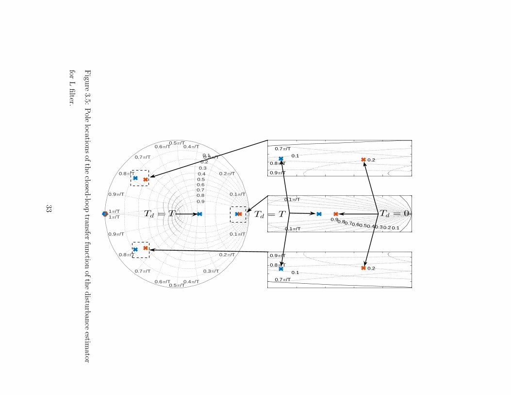
-1 -0.5 0 0.5 1-1
-0.8
-0.6
-0.4
-0.2
0
0.2
0.4
0.6
0.8
1
0.1π/T
0.1π/T
0.2π/T
0.2π/T
0.3π/T
0.3π/T0.1
0.20.30.40.5
0.9
0.6
0.80.7
0.4π/T
0.4π/T0.5π/T
0.5π/T0.6π/T
0.6π/T
0.7π/T
0.7π/T
0.8π/T
0.8π/T
0.9π/T
0.9π/T
1π/T 1π/T
0.20.1
0.7π/T
0.8π/T
0.9π/T
0.9
0.10.20.30.40.50.60.70.8
0.1π/T
0.1π/T
0.20.1
0.7π/T
0.8π/T
0.9π/T
Td = T Td = T Td = 0
Figu
re3.5:
Pole
location
sof
theclosed
-loop
transfer
function
ofthedistu
rban
ceestim
ator
forLfilter.
33
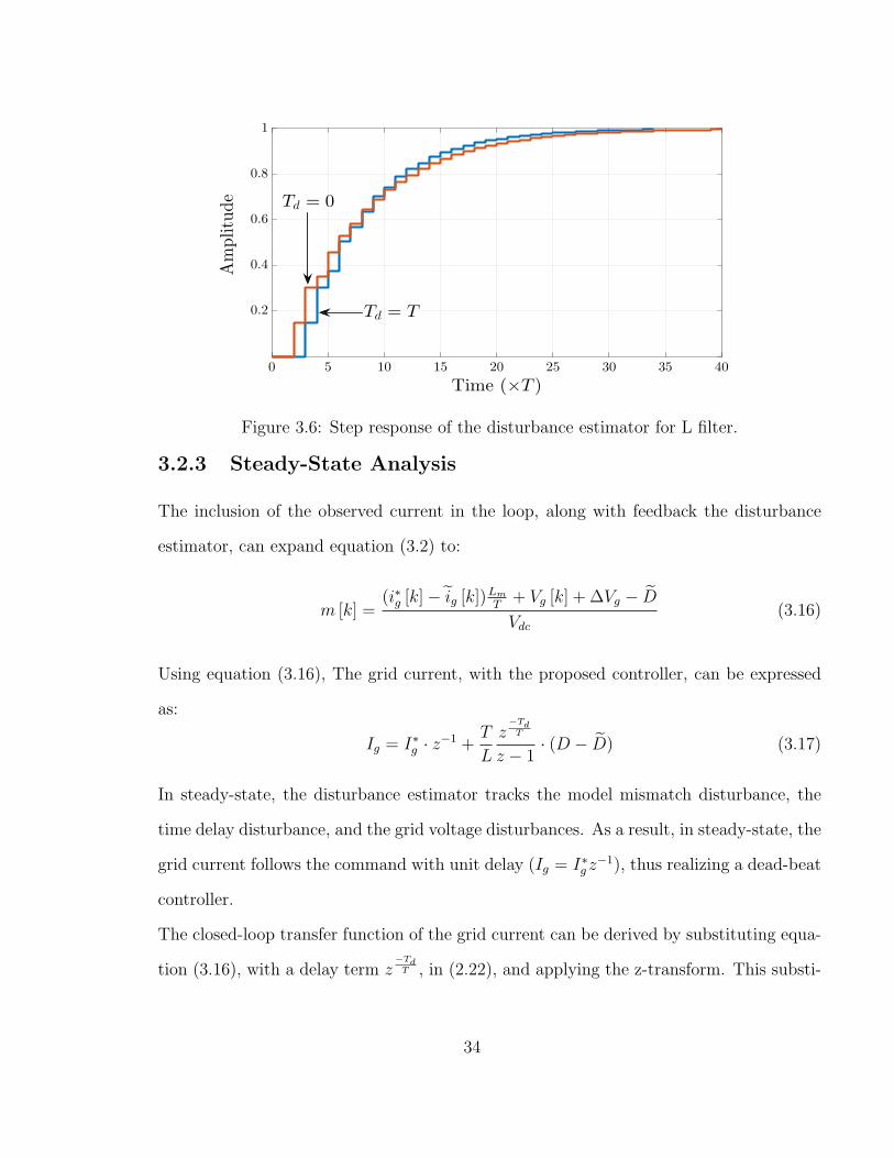
Time (×T )0 5 10 15 20 25 30 35 40
Amplitude
0.2
0.4
0.6
0.8
1
Td = T
Td = 0
Figure 3.6: Step response of the disturbance estimator for L filter.
3.2.3 Steady-State Analysis
The inclusion of the observed current in the loop, along with feedback the disturbance
estimator, can expand equation (3.2) to:
m [k] =(i∗g [k]− ig [k])
Lm
T+ Vg [k] + ∆Vg − D
Vdc
(3.16)
Using equation (3.16), The grid current, with the proposed controller, can be expressed
as:
Ig = I∗g · z−1 +T
L
z−Td
T
z − 1· (D − D) (3.17)
In steady-state, the disturbance estimator tracks the model mismatch disturbance, the
time delay disturbance, and the grid voltage disturbances. As a result, in steady-state, the
grid current follows the command with unit delay (Ig = I∗g z−1), thus realizing a dead-beat
controller.
The closed-loop transfer function of the grid current can be derived by substituting equa-
tion (3.16), with a delay term z−Td
T , in (2.22), and applying the z-transform. This substi-
34
tuting yields to (3.18)
Ig =z
−Td
T (Lm
L(z − 1) + T
LG(z))
z − 1 + TLG(z)z
−Td
T
· I∗g z−1
+TL(z
−Td
T − 1)
z − 1 + TLG(z)z
−Td
T
· Vg
+TLz
−Td
T
z − 1 + TLG(z)z
−Td
T
·∆Vg
(3.18)
It can be seen from equation (3.18) that the response of the grid current can be divided
into three responses: a response to the command I∗g , a response to the the grid voltage Vg,
and a response to the estimation error of the grid voltage ∆Vg. The following sub-sections
investigate these components.
The Current Command Component
Equation (3.18) can be re-written in term of the command I∗g , by setting Vg = 0 and
∆Vg = 0, as follow:
Ig = (Y1(z) + Y2(z)) · I∗g (3.19)
where
Y1(z) =Lm
L(z − 1)
z − 1 + TLG(z)z
−Td
T
· z−(1+Td
T) (3.20)
Y2(z) =TLG(z)
z − 1 + TLG(z)z
−Td
T
· z−(1+Td
T) (3.21)
It is worth mentioning that Y1(z) is the transfer function due to the DB controller path,
while Y2(z) is the transfer function due to the disturbance estimator path (see Figure 3.4.)
35
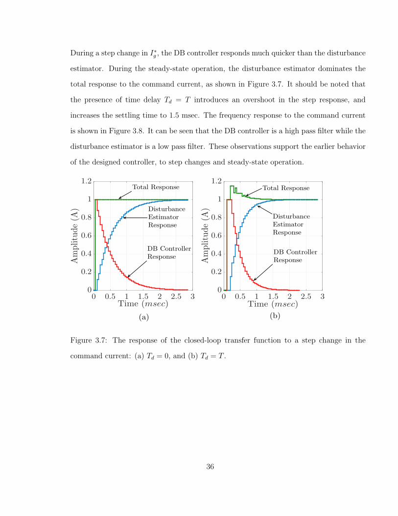
During a step change in I∗g , the DB controller responds much quicker than the disturbance
estimator. During the steady-state operation, the disturbance estimator dominates the
total response to the command current, as shown in Figure 3.7. It should be noted that
the presence of time delay Td = T introduces an overshoot in the step response, and
increases the settling time to 1.5 msec. The frequency response to the command current
is shown in Figure 3.8. It can be seen that the DB controller is a high pass filter while the
disturbance estimator is a low pass filter. These observations support the earlier behavior
of the designed controller, to step changes and steady-state operation.
Time (msec)0 0.5 1 1.5 2 2.5 3
Amplitude(A
)
0
0.2
0.4
0.6
0.8
1
1.2
Time (msec)0 0.5 1 1.5 2 2.5 3
Amplitude(A
)
0
0.2
0.4
0.6
0.8
1
1.2
(b)(a)
Total ResponseTotal Response
DB ControllerResponse
DB ControllerResponse
DisturbanceEstimatorResponse
DisturbanceEstimatorResponse
Figure 3.7: The response of the closed-loop transfer function to a step change in the
command current: (a) Td = 0, and (b) Td = T .
36

Mag
nitude(dB)
-60
-40
-20
0
20
Frequency (Hz)102 103 104
Phase(deg)
-360
-180
0
180
Mag
nitude(dB)
-60
-40
-20
0
20
Frequency (Hz)102 103 104
Phase(deg)
-360
-180
0
180
(a) (b)
Total Response Total Response
DisturbanceEstimatorDB Controller
DB Controller
Total ResponseDisturbanceEstimator
DisturbanceEstimator
DB Controller
DisturbanceEstimator
Total Response
DB Controller
Figure 3.8: The frequency response of the closed-loop transfer function to the command
current: (a) Td = 0, and (b) Td = T .
Equation (3.20) shows that the response to the command current is affected by the mis-
match ratio Lm/L. In an ideal case, Lm = L, however, in non-ideal situations, the
inductance L may vary during the operation of the 1φ dc-ac PECs. Such changes in L
can be due to the nonlinearity of L, along with the grid side effects [21]. In order to
consider the possible variations in L, the ratio κL can be defined as:
κL =Lm
L(3.22)
The response to a step change in the command current is shown in Figure 3.9 for different
values of κL. It can be seen from Figure 3.9 (a) that when Td = 0 and κL = 1, the response
is a dead-beat, i.e. one sample delay between the input and the output. However, when
the Td = T and κL = 1, the response has a minor overshoot as shown in Figure 3.9
(b), and it reaches a steady-state value in about 1.5 msec. Furthermore, as κL becomes
greater than one (L < Lm), the response overshoot increases, maintains its reach to a
steady-state value within 1.5 msec. Finally, as κL becomes less than one (L > Lm), the
controller response becomes slower. Nonetheless, the controller maintains stable response
37
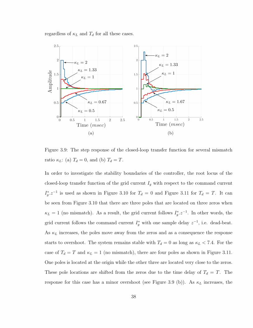
regardless of κL and Td for all these cases.
Time (msec)0 0.5 1 1.5 2 2.5
Amplitude
0
0.5
1
1.5
2
2.5
Time (msec)0 0.5 1 1.5 2 2.5
0
0.5
1
1.5
2
2.5
(b)
κL = 2
κL = 1.33
κL = 1
κL = 0.67
κL = 0.5
κL = 1.67
κL = 1.33
κL = 1
κL = 2
(a)
κL = 0.5
Figure 3.9: The step response of the closed-loop transfer function for several mismatch
ratio κL: (a) Td = 0, and (b) Td = T .
In order to investigate the stability boundaries of the controller, the root locus of the
closed-loop transfer function of the grid current Ig with respect to the command current
I∗g .z−1 is used as shown in Figure 3.10 for Td = 0 and Figure 3.11 for Td = T . It can
be seen from Figure 3.10 that there are three poles that are located on three zeros when
κL = 1 (no mismatch). As a result, the grid current follows I∗g .z−1. In other words, the
grid current follows the command current I∗g with one sample delay z−1, i.e. dead-beat.
As κL increases, the poles move away from the zeros and as a consequence the response
starts to overshoot. The system remains stable with Td = 0 as long as κL < 7.4. For the
case of Td = T and κL = 1 (no mismatch), there are four poles as shown in Figure 3.11.
One poles is located at the origin while the other three are located very close to the zeros.
These pole locations are shifted from the zeros due to the time delay of Td = T . The
response for this case has a minor overshoot (see Figure 3.9 (b)). As κL increases, the
38

poles shift further away from the zero locations and the overshoot of the dynamic response
becomes higher. Nonetheless, the system stay stable for Td = T as long as κL < 5.3.
0.2 /T
0.3 /T
0.4 /T
0.9
0.5 /T0.6 /T
0.7 /T
0.8 /T
0.9 /T
1 /T
0.1 /T
0.2 /T
0.3 /T0.7 /T
0.4 /T0.5 /T
0.6 /T
0.8 /T
0.9 /T
1 /T
0.1 /T
0.10.2
0.30.40.50.60.70.8
Figure 3.10: Root locus of the closed-loop transfer function of the grid-tied 1φ dc-ac PEC
with L-type filter for Td = 0.
39
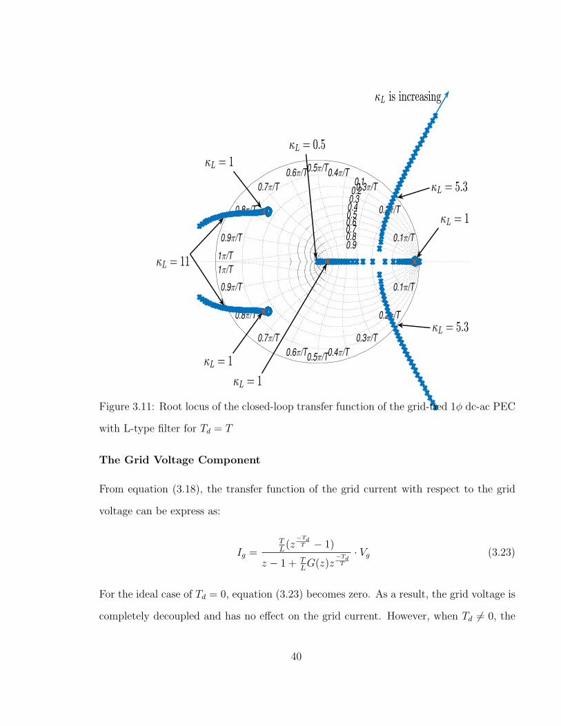
-1.5 -1 -0.5 0 0.5 1 1.5
-1.5
-1
-0.5
0
0.5
1
1.5
0.6 /T
0.7 /T
0.8 /T
0.9 /T
1 /T
0.1 /T
0.2 /T
0.3 /T
0.4 /T0.5 /T
0.6 /T
0.7 /T
0.8 /T
0.9 /T
1 /T
0.1 /T
0.2 /T
0.3 /T
0.4 /T0.5 /T
0.10.2
0.30.40.50.60.70.80.9
Figure 3.11: Root locus of the closed-loop transfer function of the grid-tied 1φ dc-ac PEC
with L-type filter for Td = T
The Grid Voltage Component
From equation (3.18), the transfer function of the grid current with respect to the grid
voltage can be express as:
Ig =TL(z
−Td
T − 1)
z − 1 + TLG(z)z
−Td
T
· Vg (3.23)
For the ideal case of Td = 0, equation (3.23) becomes zero. As a result, the grid voltage is
completely decoupled and has no effect on the grid current. However, when Td 6= 0, the
40
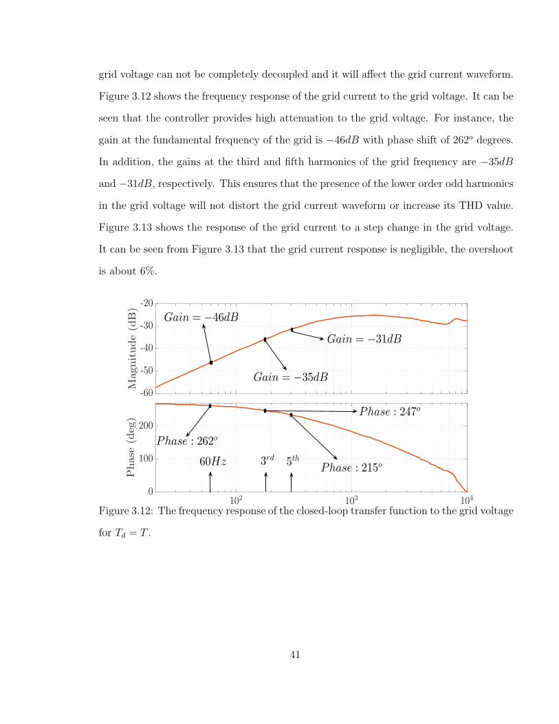
grid voltage can not be completely decoupled and it will affect the grid current waveform.
Figure 3.12 shows the frequency response of the grid current to the grid voltage. It can be
seen that the controller provides high attenuation to the grid voltage. For instance, the
gain at the fundamental frequency of the grid is −46dB with phase shift of 262o degrees.
In addition, the gains at the third and fifth harmonics of the grid frequency are −35dB
and −31dB, respectively. This ensures that the presence of the lower order odd harmonics
in the grid voltage will not distort the grid current waveform or increase its THD value.
Figure 3.13 shows the response of the grid current to a step change in the grid voltage.
It can be seen from Figure 3.13 that the grid current response is negligible, the overshoot
is about 6%.
Magnitude(dB)
-60
-50
-40
-30
-20
102 103 104
Phase
(deg)
0
100
200
60Hz 3rd 5th
Gain = −46dB
Phase : 262o
Gain = −31dB
Phase : 247o
Phase : 215o
Gain = −35dB
Figure 3.12: The frequency response of the closed-loop transfer function to the grid voltage
for Td = T .
41
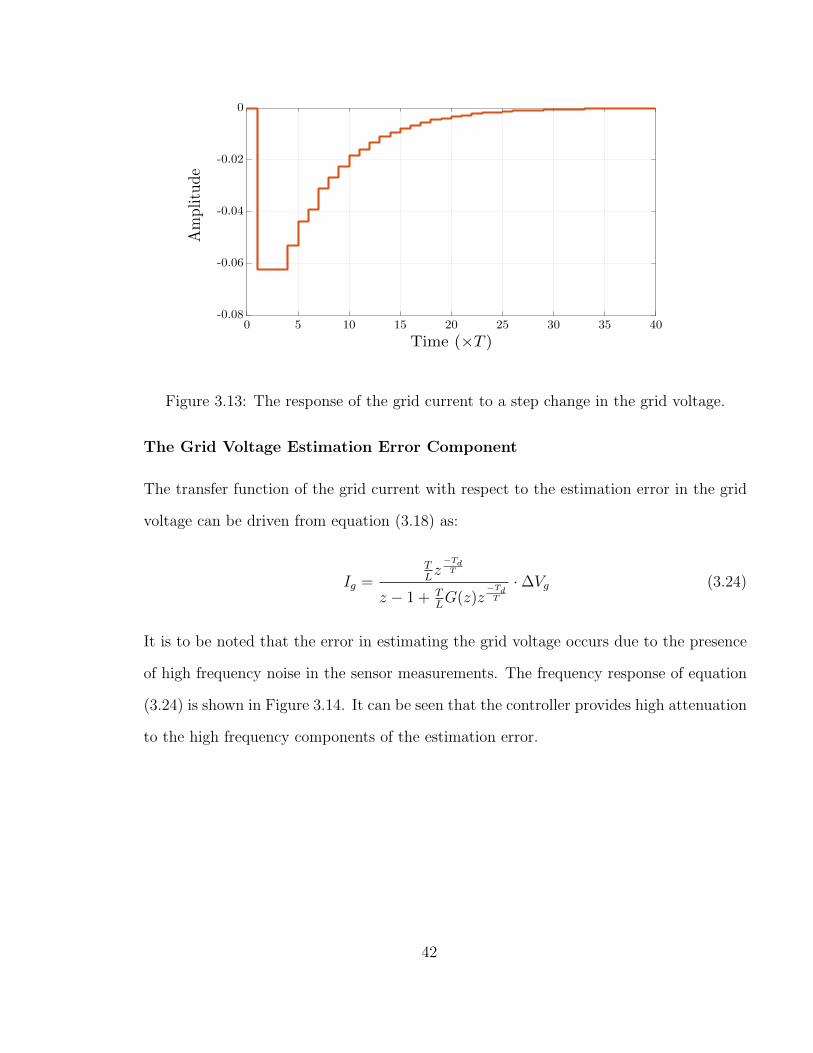
Time (×T )0 5 10 15 20 25 30 35 40
Amplitude
-0.08
-0.06
-0.04
-0.02
0
Figure 3.13: The response of the grid current to a step change in the grid voltage.
The Grid Voltage Estimation Error Component
The transfer function of the grid current with respect to the estimation error in the grid
voltage can be driven from equation (3.18) as:
Ig =TLz
−Td
T
z − 1 + TLG(z)z
−Td
T
·∆Vg (3.24)
It is to be noted that the error in estimating the grid voltage occurs due to the presence
of high frequency noise in the sensor measurements. The frequency response of equation
(3.24) is shown in Figure 3.14. It can be seen that the controller provides high attenuation
to the high frequency components of the estimation error.
42

Magnitude(dB)
-50
-40
-30
-20
-10
0
102 103 104
Phase
(deg)
-300
-200
-100
0
Td = T
Td = T
Td = 0
Td = 0
Figure 3.14: The frequency response of the closed-loop transfer function to the grid voltage
estimation error.
3.3 Dead-Beat Current Controller for a Grid-
Connected 1φ VS DC-AC PEC with LCL-Type
Filter
Figure 3.15 shows the schematic diagram of a grid-connected 1φ dc-ac PECs with LCL
filter. Similar to the 1φ dc-ac PECs with L filter, the current controller uses the mea-
surements of the grid current ig, the grid voltage vg, and the dc voltage vdc to determine
the modulation index m required to generate the switching signal, to operate the dc-ac
PEC, so that ig(t) ≈ i∗g(t). This controller consists of three main components: a DBCC,
a disturbance estimator and an observer as shown by the block diagram in Figure 3.16.
The following sub-sections present the development and the design of each of these com-
ponents.
43

Figure 3.15: A schematic diagram for grid-connected 1φ VS dc-ac PECs with LCL filter.
Figure 3.16: Block diagram of the grid-tied 1φ VS dc-ac PEC with LCL-type filter con-
trolled by the proposed controller.
3.3.1 Dead-Beat Current Controller
The continuous state space model of a grid-connected 1φ VS dc-ac PECs, with LCL filter,
can be derived as detailed in Appendix A. The derivation of the state-space model can
be accomplished by two KVL equations as:
v0(t)− L1diodt
− vc(t) = 0 (3.25)
44

vc(t)− L2digdt
− vg(t) = 0 (3.26)
Solving for vc(t) yields to:
vc(t) = L2digdt
+ vg(t) (3.27)
The first KVL, equation (3.25), can be stated as:
v0(t)− L1diodt
− L2digdt
− vg(t) = 0 (3.28)
The differential terms in (3.28) can be approximated using finite difference approximation
as:
di(t)
dt≈ ∆i(t)
∆t=
i(k + 1)− i(k)
T(3.29)
Substituting equation (3.29) in equation (3.28) and re-arranging the equation yields to:
L2
T
(ig(k + 1)− ig(k)
)+
L1
T
(io(k + 1)− io(k)
)= V0(k)− Vg(k) (3.30)
where V0(k) and Vg(k) are the average output voltage and average grid voltage over T ,
respectively. It should be noted that the average output voltage is given by:
V0(k) = m(k)Vdc (3.31)
where m(k) is the modulation index over T , while Vdc is the dc voltage. From Figure 3.15,
the current io(k + 1) can be expressed as:
io(k + 1) = ig(k + 1) + ic(k + 1) (3.32)
45

where ic(k+1) is the capacitor current at sample k+1. Equation (3.30) can be simplified
using equations (3.31) and (3.32) as:
L1 + L2
Tig(k + 1)− L2
Tig(k)−
L1
Tio(k) +
L1
Tic(k + 1) = m(k)Vdc − Vg(k) (3.33)
The capacitor current can be considered as disturbance, that is:
Dcap = −L1
Tic(k + 1) (3.34)
As a result, equation (3.33) becomes:
L1 + L2
Tig(k + 1)− L2
Tig(k)−
L1
Tio(k)−Dcap = m(k)Vdc − Vg(k) (3.35)
Re-arranging equation (3.35) to solve for m(k) as:
m(k) =L1+L2
Tig(k + 1)− L2
Tig(k)− L1
Tio(k)−Dcap + Vg(k)
Vdc
(3.36)
Equation (3.36) indicates that it is possible to adapt the controller developed in the
previous section for a grid-connected 1φ dc-ac PECs with LCL filter. Although the system
is a third order system, the assumption that the capacitor current ic can be considered
as a disturbance, can facilitate the adaption of such controller. This controller is given
by equation (3.37). It should be noted that Lmj is the inductance programmed value in
the controller for inductor j, D is the estimated disturbance given by the estimator (see
section 3.3.3), and ∆Vg(k) is the error in approximating the average grid voltage Vg(k)
over T .
m(k) =βi∗g(k) +Kcx(k)− D(k) + Vg(k) + ∆Vg(k)
Vdc
(3.37)
46
where
β =Lm1 + Lm2
T(3.38)
Kc =
−Lm1/T
0
−Lm2/T
(3.39)
x(k) =
io(k)
vc(k)
ig(k)
(3.40)
For the controller given in equation (3.37), the grid current response in an ideal operating
condition is given by:
ig(k + 1) = i∗g(k) +T
L1 + L2
(Dcap(k)− D(k)
)(3.41)
where an ideal condition implies that Lm1 = L1, Lm2 = L2, io(k) = io(k), ig(k) = ig(k),
∆Vg(k) = 0, and Td = 0. In order to achieve dead-beat response, the estimator D must
track the capacitor current disturbance Dcap in the ideal operating condition. In practical
conditions, there may be model mismatches (Lm1 6= L1 and/or Lm2 6= L2), observer error
(io(k) 6= io(k) and/or ig(k) 6= ig(k)), grid voltage disturbance (∆Vg(k) 6= 0), and controller
time delay (Td 6= 0). The aforementioned disturbances mandate that the estimator D has
to track them all.
47

3.3.2 Observer
The model of the observer is designed based on the derivation detailed in Chapter 2, that
is:
x(k + 1) =Adx(k) + BdU(k) (3.42)
ig(k) =Cdx(k) (3.43)
where
Ad = eAT (3.44)
Bd =
∫ T
0
eAυBdυ (3.45)
Cd = [0 0 1] (3.46)
A =
0 −1/Lm1 0
1/Cm −α −1/Cm
0 1/Lm2 0
(3.47)
B =
1/Lm1 0
Rm/Lm1 Rm/Lm2
0 −1/Lm2
(3.48)
(3.49)
α =Rm(Lm1 + Lm2)
Lm1Lm2
(3.50)
48
The input U(k) of the observer is given by:
U(k) = [m(k)Vdc Vg(k) + ∆Vg(k)]T (3.51)
where m(k) acts as the modulation index for the observer, and is given by:
m(k) =βi∗g(k) +Kcx(k) + Vg(k) + ∆Vg(k)
Vdc
(3.52)
It is to be noted that the error in the grid voltage measurements, ∆Vg(k), appears in the
input vector U(k) and in the modulation index m(k). Hence, ∆Vg(k) will be canceled
out and it has no effect on the observer response. Moreover, there is no model mismatch
between the observer and the controller since both has identical parameters. In addition,
the time delay can be assumed to be zero since the controller and the observer are both
implemented digitally. It is worth mentioning that m(k) does not include the estimated
disturbance D. These assumptions lead to conclude that the observed grid current ig(k)
has a response similar to equation (3.41) with D = 0, that is:
ig(k + 1) =i∗g(k) +T
Lm1 + Lm2
Dcap(k) (3.53)
=i∗g(k)−Lm1
Lm1 + Lm2
ic(k + 1)
Where
Dcap = −Lm1
Tic(k + 1) (3.54)
Similarly, the response of the observed inverter current io(k) can be driven by re-writing
49
equation (3.33) in terms of the observed values as:
Lm1 + Lm2
Tig(k + 1)− Lm2
Tig(k)−
Lm1
Tio(k) +
Lm1
Tic(k + 1) = m(k)Vdc − Vg(k)−∆Vg(k)
(3.55)
The observed grid current ig(k + 1) can be expressed in terms of the observed inverter
current as:
ig(k + 1) = io(k + 1)− ic(k + 1) (3.56)
Substituting equations (3.52) and (3.56) into equation (3.55) yields to:
io(k + 1) =i∗g(k) +Lm2
Lm1 + Lm2
ic(k + 1) (3.57)
Equations (3.53) and (3.57) show that the observed current contains an error term, which
is due to adopting a controller of a first order system to a third order one.
3.3.3 Disturbance Estimator
The grid current response under an ideal operating condition is given by equation (3.41).
However, in practical operating conditions, the grid current response can be expressed by
equation (3.58) (see the detailed derivation in Appendix A).
Ig =I∗g · z−2 +T
L1+L2
z(z − 1)(D − D) (3.58)
where D is the total disturbance which is given by:
D(z) =I∗g · z−2Lm1 − L1 + Lm2 − L2
Tz(z − 1)− Ic
L1
Tz(z − 1) + Vg(z − 1) + ∆Vg (3.59)
50

The disturbance D(z) consists of four terms, which are the model mismatch (when Lm1 6=
L1 or Lm2 6= L2), capacitor current (due to the adoption of a first order controller), grid
voltage (due to the time delay which causes incomplete decoupling of the grid voltage),
and error in grid voltage measurements (when ∆Vg 6= 0). Nonetheless, the estimator is
used to compensate for these disturbances by estimating the required D such that the
controller achieves dead-beat response. The estimated disturbance D can be determined
as (see Figure 3.16):
D(z) = G(z)(Ig − Ig · z−1) (3.60)
= G(z)(Ig − I∗g · z−2 + IcLm1
Lm1 + Lm2
· z−1)
where G(z) is the transfer function of the estimator. It should be noted that for the LCL
filter, the time delay is assumed to be Td = T in order to allow enough time to implement
the third order observer. The relationship between the estimated disturbance D and the
actual disturbance D can be driven by substituting equation (3.58) in equation (3.60),
which leads to:
D(z) =T
L1+L2G(z)
z(z − 1) + TL1+L2
G(z)·D +
z(z − 1)γG(z)
z(z − 1) + TL1+L2
G(z)· Ic · z−1 (3.61)
γ =Lm1
Lm1 + Lm2
(3.62)
The estimated disturbance D will not only respond to the actual disturbance, but also to
the observed capacitor current Ic. This feature is due to the assumption that the observed
capacitor current Ic acts as a disturbance on the estimator. Let the disturbance estimator
transfer function be:
G(z) =bnz
n + bn−1zn−1 + . . .+ b1z + b0
amzm + am−1zm−1 + . . .+ a1z + a0(3.63)
51

The closed-loop characteristics equation, λ(z), can be obtained by substituting equations
(3.63) into the denominator of equation (3.61):
λ(z) =T
L1 + L2
b0 + (T
L1 + L2
b1 − a0)z + (T
L1 + L2
b2 − a1 + a0)z2
+ (T
L1 + L2
b3 − a2 + a1)z3 + . . .
(3.64)
Equation (3.64) shows that the stability of the disturbance estimator depends on the
coefficients of G(z). A stable estimator can be achieved by selecting the appropriate
coefficients. For instance, with the system given in Table 3.2, the selected coefficients are:
b0 = 1.8, b1 = 4.5, b2 = 12, bn = 0 for all n > 2, a0 = 0.25, a1 = 1, a2 = 1, and am = 0
for all m > 2. The pole locations shown in Figure 3.17 indicates that the disturbance
estimator is stable. Moreover, the step response of the estimator is shown in Figure 3.18.
It can be seen that the estimator has an response settling time of 12T .
Table 3.2: Parameters for the power electronics converter system with LCL-type filter.
Parameter Symbol ValueGrid Voltage vg 240 V
Grid Frequency fg 60 HzDC Voltage vdc 400 V
Controller Period T 50 µsecController Delay Td 50 µsec
Inventor side inductor L1 1.6 m HGrid side inductor L2 0.8 m H
Capacitor C 10µ FDamping resistor R 2.4 Ω
52

-1 -0.8 -0.6 -0.4 -0.2 0 0.2 0.4 0.6 0.8 1-1
-0.8
-0.6
-0.4
-0.2
0
0.2
0.4
0.6
0.8
1
0.1π/T
0.1π/T
0.2π/T
0.2π/T
0.3π/T
0.3π/T0.10.2
0.30.40.5
0.9
0.6
0.80.7
0.4π/T
0.4π/T0.5π/T
0.5π/T0.6π/T
0.6π/T
0.7π/T
0.7π/T
0.8π/T
0.8π/T
0.9π/T
0.9π/T
1π/T 1π/T
Figure 3.17: Pole locations of the closed-loop transfer function of the disturbance estima-
tor for LCL filter.
Time (×T )0 2 4 6 8 10 12 14 16 18 20
Amplitude(A
)
0.2
0.4
0.6
0.8
1
Figure 3.18: Step response of the disturbance estimator for LCL filter.
53
3.3.4 Steady-State Analysis
The closed-loop transfer function of the grid current Ig can be obtained by substituting
equations (3.59) and (3.61) into equation (3.58) to provide:
Ig =I∗g · z−2κLz(z − 1) + T
L1+L2G(z)
z(z − 1) + TL1+L2
G(z)
− Ic
L1L1+L2
z(z − 1)
z(z − 1) + TL1+L2
G(z)
− Ic · z−1γ TL1+L2
G(z)
z(z − 1) + TL1+L2
G(z)(3.65)
− Vg
TL1+L2
(z − 1)
z(z − 1) + TL1+L2
G(z)
+ ∆Vg
TL1+L2
z(z − 1) + TL1+L2
G(z)
κL =Lm1 + Lm2
L1 + L2
(3.66)
Equation (3.65) indicates that the response of the grid current can be divided into five
components, which are: the response to the command I∗g , response to the capacitor current
Ic, response to the observed capacitor current Ic, response to the grid voltage Vg, and
response to the estimation error of the grid voltage ∆Vg. The following sub-sections
investigate each of these components.
54
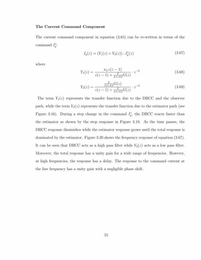
The Current Command Component
The current command component in equation (3.65) can be re-written in terms of the
command I∗g :
Ig(z) = (Y1(z) + Y2(z)) · I∗g (z) (3.67)
where
Y1(z) =κLz(z − 1)
z(z − 1) + TL1+L2
G(z)· z−2 (3.68)
Y2(z) =T
L1+L2G(z)
z(z − 1) + TL1+L2
G(z)· z−2 (3.69)
The term Y1(z) represents the transfer function due to the DBCC and the observer
path, while the term Y2(z) represents the transfer function due to the estimator path (see
Figure 3.16). During a step change in the command I∗g , the DBCC reacts faster than
the estimator as shown by the step response in Figure 3.19. As the time passes, the
DBCC response diminishes while the estimator response grows until the total response is
dominated by the estimator. Figure 3.20 shows the frequency response of equation (3.67).
It can be seen that DBCC acts as a high pass filter while Y2(z) acts as a low pass filter.
Moreover, the total response has a unity gain for a wide range of frequencies. However,
at high frequencies, the response has a delay. The response to the command current at
the line frequency has a unity gain with a negligible phase shift.
55
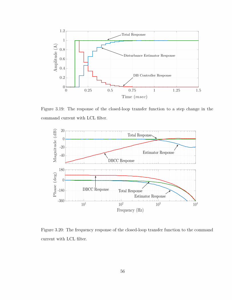
Time (msec)
0 0.25 0.5 0.75 1 1.25 1.5
Amplitude(A
)
0
0.2
0.4
0.6
0.8
1
1.2Total Response
Disturbance Estimator Response
DB Controller Response
Figure 3.19: The response of the closed-loop transfer function to a step change in the
command current with LCL filter.
Magnitude(dB)
-40
-20
0
20
Frequency (Hz)101 102 103 104
Phase
(deg)
-360
-180
0
180
DBCC Response
DBCC Response
Estimator Response
Total Response
Total ResponseEstimator Response
Figure 3.20: The frequency response of the closed-loop transfer function to the command
current with LCL filter.
56
-1 -0.5 0 0.5 1
-1.5
-1
-0.5
0
0.5
1
1.5
0.1π/T
0.1π/T
0.2π/T
0.2π/T
0.3π/T
0.3π/T
0.1
0.2
0.3
0.40.5
0.9
0.6
0.80.7
0.4π/T
0.4π/T
0.5π/T
0.5π/T0.6π/T
0.6π/T
0.7π/T
0.7π/T
0.8π/T
0.8π/T
0.9π/T
0.9π/T
1π/T
1π/T
κL = 1
Zeros
κL = 0.033
κL = 0.033
κL = 7
Figure 3.21: Root locus of the closed-loop transfer function of the grid-tied 1φ dc-ac PEC
with respect to κL.
The effect of varying the inductors of the LCL filter can be investigated using κL. The
pole locations of equation (3.67) with respect to κL are shown in Figure 3.21. For the
case of κL = 1, double poles are located on the origin point, and four poles are located
exactly on four zeros as shown in Figure 3.21. As κL increases, the poles move away from
the zeros toward the boundaries of the unit circle. Hence, the response starts to have an
overshoot and becomes under-damped. The magnitude of the overshoot is proportional
to the distance between the poles and zeros. Nonetheless, the system remains stable as
long as 0.033 < κL < 7.
57
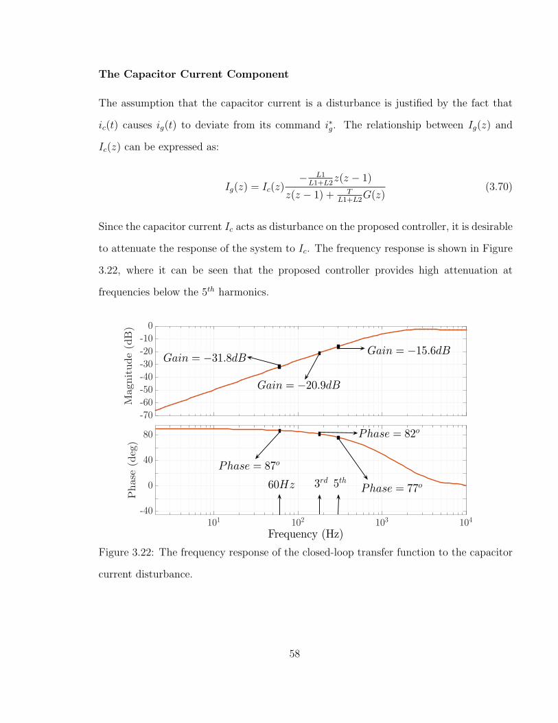
The Capacitor Current Component
The assumption that the capacitor current is a disturbance is justified by the fact that
ic(t) causes ig(t) to deviate from its command i∗g. The relationship between Ig(z) and
Ic(z) can be expressed as:
Ig(z) = Ic(z)− L1
L1+L2z(z − 1)
z(z − 1) + TL1+L2
G(z)(3.70)
Since the capacitor current Ic acts as disturbance on the proposed controller, it is desirable
to attenuate the response of the system to Ic. The frequency response is shown in Figure
3.22, where it can be seen that the proposed controller provides high attenuation at
frequencies below the 5th harmonics.
Magnitude(dB)
-70
-60
-50
-40
-30
-20
-10
0
101 102 103 104
Phase
(deg)
-40
0
40
80
3rd 5th60Hz
Frequency (Hz)
Gain = −20.9dB
Gain = −31.8dBGain = −15.6dB
Phase = 82o
Phase = 77o
Phase = 87o
Figure 3.22: The frequency response of the closed-loop transfer function to the capacitor
current disturbance.
58

The Observed Capacitor Current Component
Section 3.3.2 has shown that the observer tracks the current Ig and Io with an error term
(equations (3.53) and (3.57)). This error term, which is due to the observed capacitor
current, appears in Ig response as a disturbance (see equation (3.65)). The relationship
of Ig(z) and Ic(z) can be expressed as:
Ig(z) = Ic(z) · z−1−γ T
L1+L2G(z)
z(z − 1) + TL1+L2
G(z)(3.71)
The frequency response of equation (3.71) is shown in Figure 3.23. It can be seen that
the proposed controller provides attenuation greater than −4 dB.
Magnitude(dB)
-30
-20
-10
0
101 102 103 104
Phase
(deg)
-150
-100
-50
0
3rd 5th60Hz
Frequency (Hz)
Gain = −4.3dB
Phase = −11o
Phase = 18o
Phase = −4o
Gain = −4.1dBGain = −4.2dB
Figure 3.23: The frequency response of the closed-loop transfer function to the observed
capacitor current disturbance.
59
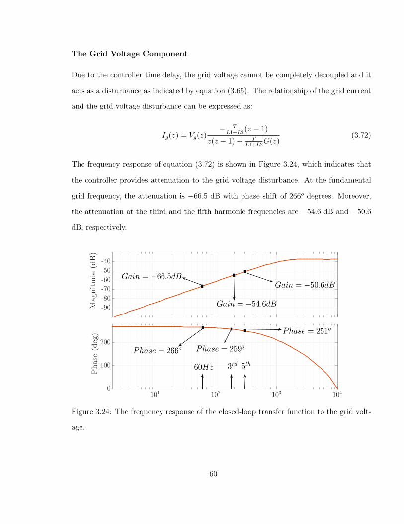
The Grid Voltage Component
Due to the controller time delay, the grid voltage cannot be completely decoupled and it
acts as a disturbance as indicated by equation (3.65). The relationship of the grid current
and the grid voltage disturbance can be expressed as:
Ig(z) = Vg(z)− T
L1+L2(z − 1)
z(z − 1) + TL1+L2
G(z)(3.72)
The frequency response of equation (3.72) is shown in Figure 3.24, which indicates that
the controller provides attenuation to the grid voltage disturbance. At the fundamental
grid frequency, the attenuation is −66.5 dB with phase shift of 266o degrees. Moreover,
the attenuation at the third and the fifth harmonic frequencies are −54.6 dB and −50.6
dB, respectively.
Frequency (Hz)
Magnitude(dB)
-90
-80
-70
-60
-50
-40
101 102 103 104
Phase
(deg)
0
100
200
60Hz 3rd 5th
Phase = 266o Phase = 259o
Phase = 251o
Gain = −50.6dB
Gain = −54.6dB
Gain = −66.5dB
Figure 3.24: The frequency response of the closed-loop transfer function to the grid volt-
age.
60

The Grid Voltage Estimation Error Component
Another source of disturbance in the grid current response is the error in estimating the
grid voltage ∆Vg. This is due to high frequency noise in the sensor measurements. In
order to investigate the controller response to ∆Vg disturbance, the relationship of Ig(z)
and ∆Vg(z) can be expressed as:
Ig(z) = ∆Vg(z)T
L1+L2
z(z − 1) + TL1+L2
G(z)(3.73)
The frequency response of equation (3.73) is shown in Figure 3.25. It can be seen from
Figure 3.25 that the controller attenuate ∆Vg disturbance especially at higher frequencies.
Magnitude(dB)
-50
-40
-30
-20
101 102 103 104
Phase
(deg)
-300
-200
-100
0
Frequency (Hz)Figure 3.25: The frequency response of the closed-loop transfer function to grid voltage
estimation error.
61
3.4 Summary
In this chapter, the design and implementation of a dead-beat current controller with
disturbance estimator for grid-connected 1φ VS dc-ac PECs have been presented. Two
types of grid-tied filters for interconnecting the PEC to the host grid have been consid-
ered; the L-type filter and LCL-type filter. The presented controllers are set for accurate
regulation of the power delivered to the grid, while meeting the standards and industrial
codes. In addition to meeting these constrains, the proposed controller can operate the
grid-connected 1φ VS dc-ac PEC with negligible sensitivity to different types of distur-
bances. In this chapter, it has been shown that for grid-connected 1φ VS dc-ac PEC
with L-type filter, there are three main sources of disturbances: parameter variation, grid
voltage, and measurements error. On the other hand, there are five sources of distur-
bances for grid-connected 1φ VS dc-ac PEC with LCL-type filter, when operated by the
proposed controller. These disturbances are parameter variation, grid voltage, capacitor
current, measurements error, and observer error. Nonetheless, it has been shown that the
response of the grid-connected 1φ VS dc-ac PEC when operated by the proposed con-
troller has negligible sensitivity to these disturbances. The next chapter provides details
implementation of the developed controller and observer for performance evaluation. The
performance evaluation is carried out by simulation under different operating conditions.
62

Chapter 4
Performance Evaluation: Simulation
Studies
4.1 Overview
The previous chapter has presented several dead-beat current controllers, which are de-
signed to operate single-phase interconnected dc-ac power electronic converters. The de-
veloped BDCCs have been featured with disturbance estimators to compensate for model
mismatches and/or deviations in measured values. Furthermore, Chapter 3 has presented
DBCCs for different types of grid-tied filters (the L and LCL filters) that are widely
used in 1φ interconnected VS dc-ac PECs. The analysis, stability, and responses of the
developed DBCCs have demonstrated promising performance that is complemented by
minor sensitivity to changes in systems parameters.
This chapter presents the performance evaluation that is carried out through simula-
tion tests under different operating conditions. Moreover, simulation results obtained for
the developed DBCCs are compared with results obtained from the predictive current
controller, with delay compensator [84] (PCDC), and traditional predictive controller
63

(TPC) [85] under similar operating conditions.
4.2 Performance Indices
In order to evaluate the performance of the proposed controller, three indices are selected:
the relative error in the root-mean-square current (ERMS), power factor (PF), and total
harmonic distortion (THD) factor.
4.2.1 Relative Error
The ERMS is calculated using equation (4.1), that is:
ERMS =
∣∣∣I∗g(rms) − Ig(rms)
∣∣∣I∗g(rms)
100% (4.1)
where I∗g(rms) is the rms value of the command current and the Ig(rms) is the rms value of
the injected current to the grid. A low value of ERMS implies that the injected current to
the grid closely follows its command. The value of Ig(rms) is measured using the HIOKI
PW3198 Power Quality Analyzer.
4.2.2 Power Factor
Power factor (PF) is selected to examine the phase shift between the instantaneous com-
mand current I∗g (t) and instantaneous current injected to the grid Ig(t). The PF index is
determined as:
PF = cos(θv − θi∗ − θi) (4.2)
where θv is the phase shift of the grid voltage, θi∗ is the phase shift of I∗g (t), and θi is
the phase of Ig(t). During the experimental tests, the PF index was obtained using the
64

HIOKI PW3198 Power Quality Analyzer. It should be noted that the PF is not used in
the control action, however, it is a good indication of how well the grid current follows its
command.
4.2.3 Total Harmonic Distortion Factor
In general, the quality of the current injected to the grid is demonstrated by the total
harmonic distortion, which is defined as:
THD =
(∞∑
n=2,3,···
I2n
) 1
2
I1(4.3)
where In is the rms value of the nth harmonic component present in Ig(t). Equation (4.3)
indicates that a high quality current is the one with a low THD. Moreover, the standards
and industrial codes require that the current injected or drawn by any PEC has to have
its THDI ≤ 5% at full load [13–15]. The value of the THD during the experimental tests
was directly measured by the HIOKI PW3198 Power Quality Analyzer.
4.3 Grid-Connected 1φ VS DC-AC PEC with L-Type
Filter
Simulation tests for the developed DBCCs were carried out for controlling dc-ac PEC with
L-type filter. Figure 4.1 shows the block diagram of the DBCC used in these simulation
tests. The dc voltage vdc was modeled using a dc power source and an ac power source
with a frequency double of the grid frequency, i.e. 120 Hz, in order to model the ripple in
the dc voltage of a real system. The grid voltage vg was modeled using an ac power source.
In real system, the command current i∗g is generated by an outer loop controller, the dc
65
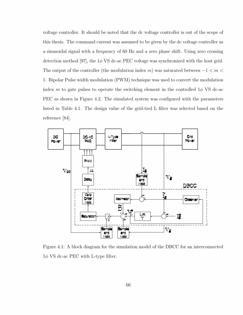
voltage controller. It should be noted that the dc voltage controller is out of the scope of
this thesis. The command current was assumed to be given by the dc voltage controller as
a sinusoidal signal with a frequency of 60 Hz and a zero phase shift. Using zero crossing
detection method [97], the 1φ VS dc-ac PEC voltage was synchronized with the host grid.
The output of the controller (the modulation index m) was saturated between −1 < m <
1. Bipolar Pulse width modulation (PWM) technique was used to convert the modulation
index m to gate pulses to operate the switching element in the controlled 1φ VS dc-ac
PEC as shown in Figure 4.2. The simulated system was configured with the parameters
listed in Table 4.1. The design value of the grid-tied L filter was selected based on the
reference [84].
Figure 4.1: A block diagram for the simulation model of the DBCC for an interconnected
1φ VS dc-ac PEC with L-type filter.
66

Figure 4.2: A block diagram for the bipolar Pulse width modulation (PWM) technique.
Table 4.1: Parameters for the simulation model of the DBCC for the L-type filter.
Parameter Symbol ValueGrid Voltage vg 240 V
Grid Frequency fg 60 HzDC Voltage vdc 400 V
Switching Frequency - 10 kHzController Period T 50 µsecController Delay Td 25 µsecFilter Inductance L 0.8 mH
b1 2.4Disturbance b0 2.4Estimator a2 1Coefficients a1 1
a0 0.5
4.3.1 Steady-State Simulation Studies
The steady-state simulation of the DBCC was investigated under different types of dis-
turbances. These studies were conducted with a command current I∗g (t) as:
i∗g(t) = 30 sin(120πt) [A] (4.4)
Figure 4.3 shows the steady-state simulation results for Td = 0.5T and κL = 1. In this
case, the grid voltage was acting as disturbance due to the time delay (see equation
67
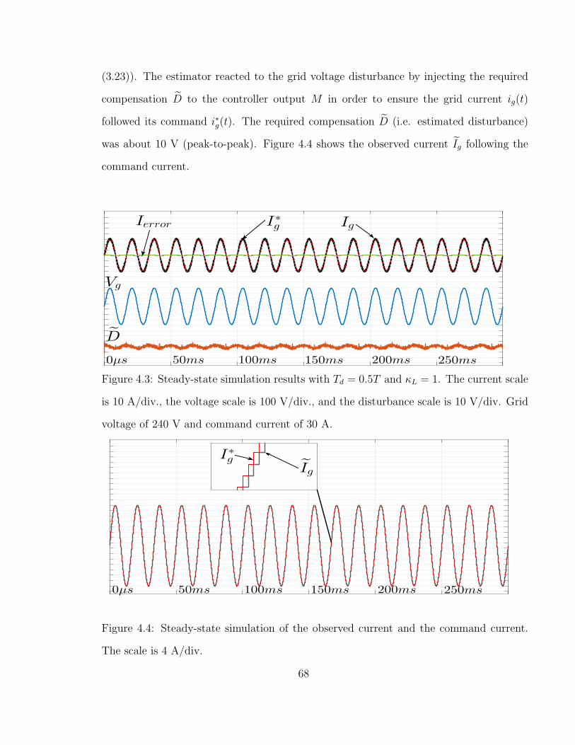
(3.23)). The estimator reacted to the grid voltage disturbance by injecting the required
compensation D to the controller output M in order to ensure the grid current ig(t)
followed its command i∗g(t). The required compensation D (i.e. estimated disturbance)
was about 10 V (peak-to-peak). Figure 4.4 shows the observed current Ig following the
command current.
D
0µs 50ms 100ms 150ms 200ms 250ms
Vg
Ierror IgI∗g
Figure 4.3: Steady-state simulation results with Td = 0.5T and κL = 1. The current scale
is 10 A/div., the voltage scale is 100 V/div., and the disturbance scale is 10 V/div. Grid
voltage of 240 V and command current of 30 A.
IgI∗g
150ms0µs 50ms 100ms 200ms 250ms
Figure 4.4: Steady-state simulation of the observed current and the command current.
The scale is 4 A/div.
68
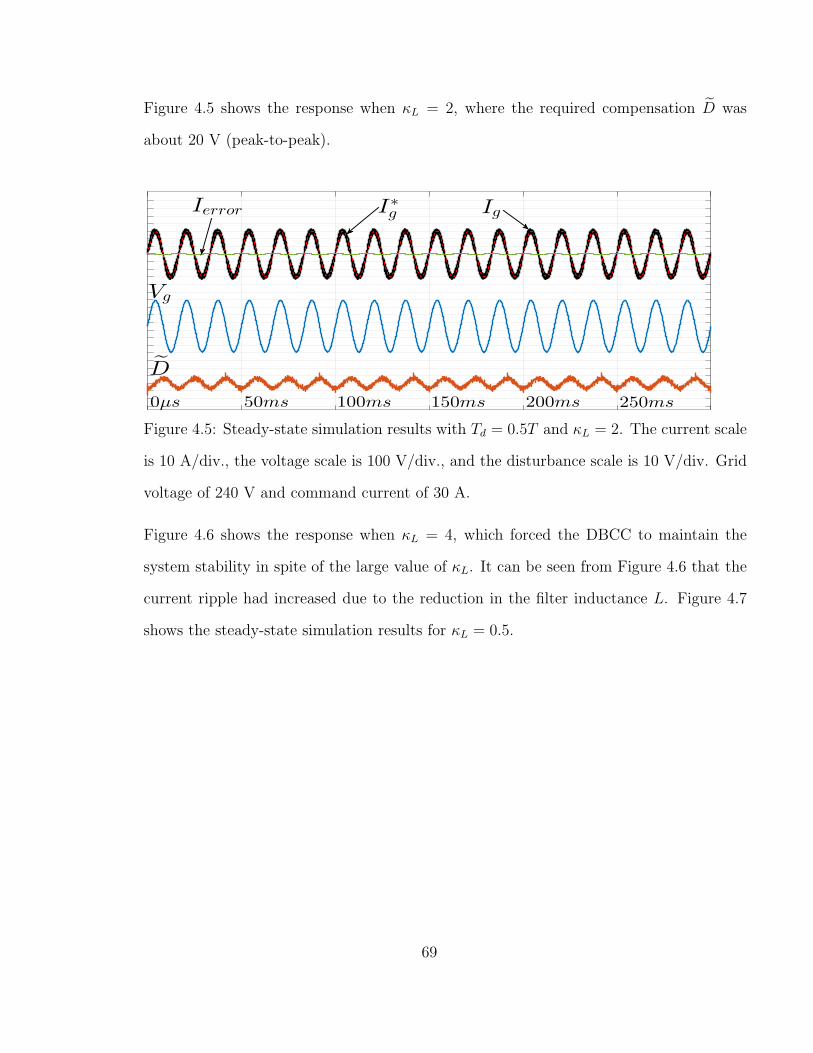
Figure 4.5 shows the response when κL = 2, where the required compensation D was
about 20 V (peak-to-peak).
D
0µs 50ms 100ms 150ms 200ms 250ms
Vg
Ierror IgI∗g
Figure 4.5: Steady-state simulation results with Td = 0.5T and κL = 2. The current scale
is 10 A/div., the voltage scale is 100 V/div., and the disturbance scale is 10 V/div. Grid
voltage of 240 V and command current of 30 A.
Figure 4.6 shows the response when κL = 4, which forced the DBCC to maintain the
system stability in spite of the large value of κL. It can be seen from Figure 4.6 that the
current ripple had increased due to the reduction in the filter inductance L. Figure 4.7
shows the steady-state simulation results for κL = 0.5.
69
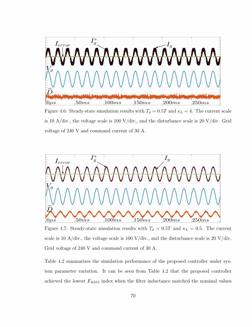
D
0µs 50ms 100ms 150ms 200ms 250ms
Vg
IerrorI∗g Ig
Figure 4.6: Steady-state simulation results with Td = 0.5T and κL = 4. The current scale
is 10 A/div., the voltage scale is 100 V/div., and the disturbance scale is 20 V/div. Grid
voltage of 240 V and command current of 30 A.
D
0µs 50ms 100ms 150ms 200ms 250ms
Vg
IerrorIgI∗g
Figure 4.7: Steady-state simulation results with Td = 0.5T and κL = 0.5. The current
scale is 10 A/div., the voltage scale is 100 V/div., and the disturbance scale is 20 V/div.
Grid voltage of 240 V and command current of 30 A.
Table 4.2 summarizes the simulation performance of the proposed controller under sys-
tem parameter variation. It can be seen from Table 4.2 that the proposed controller
achieved the lowest ERMS index when the filter inductance matched the nominal values
70
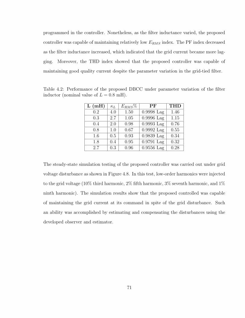
programmed in the controller. Nonetheless, as the filter inductance varied, the proposed
controller was capable of maintaining relatively low ERMS index. The PF index decreased
as the filter inductance increased, which indicated that the grid current became more lag-
ging. Moreover, the THD index showed that the proposed controller was capable of
maintaining good quality current despite the parameter variation in the grid-tied filter.
Table 4.2: Performance of the proposed DBCC under parameter variation of the filterinductor (nominal value of L = 0.8 mH).
L (mH) κL ERMS% PF THD0.2 4.0 1.50 0.9998 Lag 1.460.3 2.7 1.05 0.9996 Lag 1.150.4 2.0 0.98 0.9993 Lag 0.760.8 1.0 0.67 0.9992 Lag 0.551.6 0.5 0.93 0.9839 Lag 0.341.8 0.4 0.95 0.9791 Lag 0.322.7 0.3 0.96 0.9556 Lag 0.28
The steady-state simulation testing of the proposed controller was carried out under grid
voltage disturbance as shown in Figure 4.8. In this test, low-order harmonics were injected
to the grid voltage (10% third harmonic, 2% fifth harmonic, 3% seventh harmonic, and 1%
ninth harmonic). The simulation results show that the proposed controlled was capable
of maintaining the grid current at its command in spite of the grid disturbance. Such
an ability was accomplished by estimating and compensating the disturbances using the
developed observer and estimator.
71

0µs 50ms 100ms 150ms 200ms 250ms
D
Vg
IerrorI∗g Ig
Figure 4.8: Steady-state simulation results with Td = 0.5T , κL = 1, low-order harmonics
(3rd = 24 V, 5th = 4.8 V, 7th = 7.2 V, and 9th = 2.4 V) injected to the grid voltage. The
current scale is 10 A/div., the voltage scale is 100 V/div., and the disturbance scale is 10
V/div. Grid voltage of 240 V and command current of 30 A.
Moreover, the steady-state simulation testing of the proposed DBCC was performed under
dc voltage disturbance as shown in Figure 4.9. In this test, 10% second order ripple was
injected to the dc voltage in order to mimic the voltage variation of the dc voltage in real
systems. The simulation results show that the proposed DBCC was able to reject the dc
voltage side disturbance and maintain the grid current at its command
72
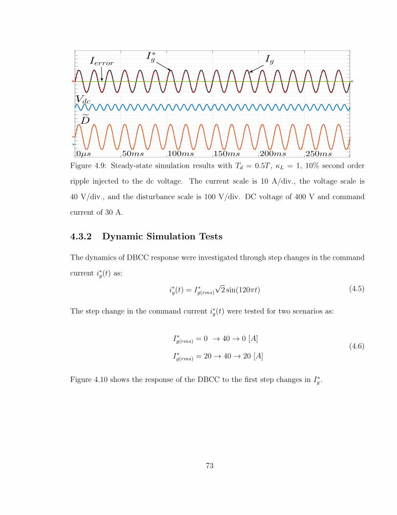
50ms 100ms 150ms 200ms 250ms
Ierror
Vdc
D
IgI∗g
0µs
Figure 4.9: Steady-state simulation results with Td = 0.5T , κL = 1, 10% second order
ripple injected to the dc voltage. The current scale is 10 A/div., the voltage scale is
40 V/div., and the disturbance scale is 100 V/div. DC voltage of 400 V and command
current of 30 A.
4.3.2 Dynamic Simulation Tests
The dynamics of DBCC response were investigated through step changes in the command
current i∗g(t) as:
i∗g(t) = I∗g(rms)
√2 sin(120πt) (4.5)
The step change in the command current i∗g(t) were tested for two scenarios as:
I∗g(rms) = 0 → 40 → 0 [A]
I∗g(rms) = 20 → 40 → 20 [A]
(4.6)
Figure 4.10 shows the response of the DBCC to the first step changes in I∗g .
73
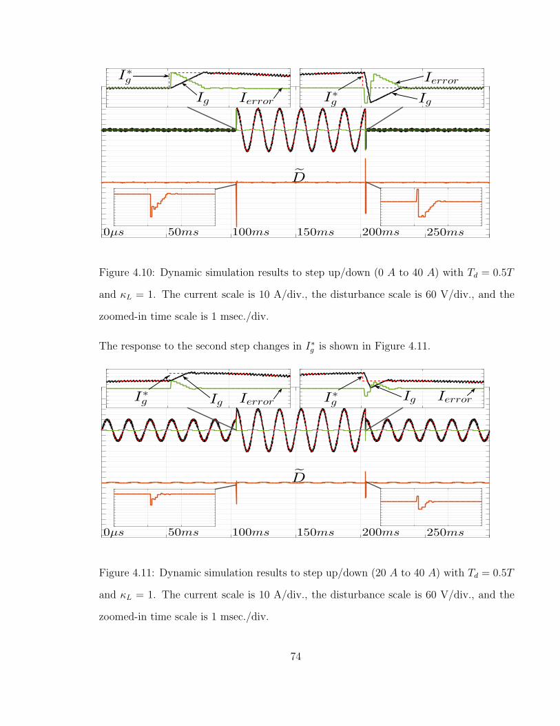
0µs 50ms 100ms 150ms 200ms 250ms
I∗gIerror
I∗g
Ig Ig
Ierror
D
Figure 4.10: Dynamic simulation results to step up/down (0 A to 40 A) with Td = 0.5T
and κL = 1. The current scale is 10 A/div., the disturbance scale is 60 V/div., and the
zoomed-in time scale is 1 msec./div.
The response to the second step changes in I∗g is shown in Figure 4.11.
0µs 50ms 100ms 150ms 200ms 250ms
I∗g
D
I∗g Ig Ig IerrorIerror
Figure 4.11: Dynamic simulation results to step up/down (20 A to 40 A) with Td = 0.5T
and κL = 1. The current scale is 10 A/div., the disturbance scale is 60 V/div., and the
zoomed-in time scale is 1 msec./div.
74

It can be seen from Figure 4.10 and Figure 4.11 that the DBCC was able to accurately
respond to the step changes in the command current. These responses were not affected
by the amount of changes in I∗g . The responses of the DBCC had a settling time close
to 0.7 msec and a minor overshoot. However, during the step down changes in I∗g , there
was a large overshoot as shown in the zoomed-in portion of the current. This overshoot
was created by the response of the estimator, which was over-damped during the step
up and under-damped during the step down. Nonetheless, the large overshoot during
the step down was not a concern for the safety operation of the 1φ VS dc-ac PEC since
the direction of this overshoot was toward the zero axis. Hence, the instantaneous grid
current never exceeded its rated value.
4.4 Grid-Connected 1φ VS DC-AC PEC with LCL-
Type Filter
The simulation tests of the developed DBCC were carried out for controlling dc-ac PEC
with an LCL-type filter. Figure 4.12 shows the block diagram of the DBCC used in
this simulation tests. The parameters of the simulation model are listed in Table 4.3.
The design value of the grid-tied LCL filter were selected based on the design given in
reference [98].
75
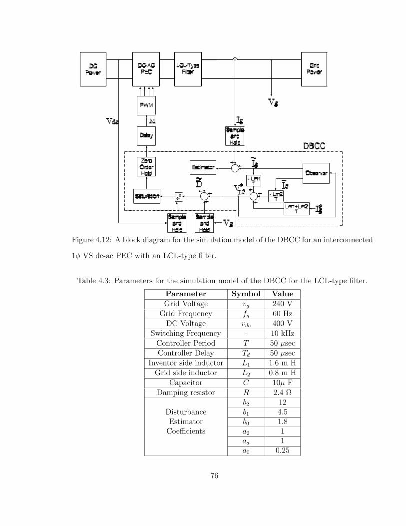
Figure 4.12: A block diagram for the simulation model of the DBCC for an interconnected
1φ VS dc-ac PEC with an LCL-type filter.
Table 4.3: Parameters for the simulation model of the DBCC for the LCL-type filter.
Parameter Symbol ValueGrid Voltage vg 240 V
Grid Frequency fg 60 HzDC Voltage vdc 400 V
Switching Frequency - 10 kHzController Period T 50 µsecController Delay Td 50 µsec
Inventor side inductor L1 1.6 m HGrid side inductor L2 0.8 m H
Capacitor C 10µ FDamping resistor R 2.4 Ω
b2 12Disturbance b1 4.5Estimator b0 1.8Coefficients a2 1
aa 1a0 0.25
76

4.4.1 Steady-State Simulation Tests
The steady-state simulation tests were conducted for a command current i∗g(t) (see equa-
tion (4.4)) and a time delay of Td = T . Figure 4.13 shows the steady-state simulation
results for κL = 1. These results show that the grid current was able to track its command
with a good accuracy.
0µs 50ms 100ms 150ms 200ms 250ms
D
Vg
IC
I∗g IgIerror
Figure 4.13: Steady-state simulation results with Td = T and κL = 1 . The current scale
is 10 A/div., the voltage scale is 100 V/div., and the disturbance scale is 10 V/div.
As κL was varied, the tracking error increased and required D became higher. For instance,
Figure 4.14 shows the case for κL = 0.75, and Figure 4.15 shows the case for κL = 1.5. In
both cases, parameters of the LCL filter were varied from their nominal values in order
to create disturbances for the controller. The estimator reacted to these disturbances by
increasing the compensation D to maintain the grid current at its command.
77
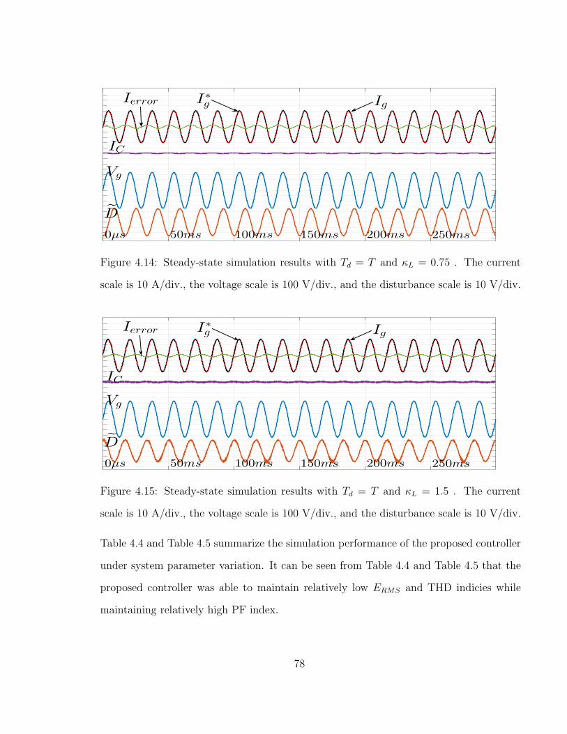
0µs 50ms 100ms 150ms 200ms 250ms
D
Vg
IC
I∗g IgIerror
Figure 4.14: Steady-state simulation results with Td = T and κL = 0.75 . The current
scale is 10 A/div., the voltage scale is 100 V/div., and the disturbance scale is 10 V/div.
0µs 50ms 100ms 150ms 200ms 250ms
D
Vg
IC
Ierror IgI∗g
Figure 4.15: Steady-state simulation results with Td = T and κL = 1.5 . The current
scale is 10 A/div., the voltage scale is 100 V/div., and the disturbance scale is 10 V/div.
Table 4.4 and Table 4.5 summarize the simulation performance of the proposed controller
under system parameter variation. It can be seen from Table 4.4 and Table 4.5 that the
proposed controller was able to maintain relatively low ERMS and THD indicies while
maintaining relatively high PF index.
78
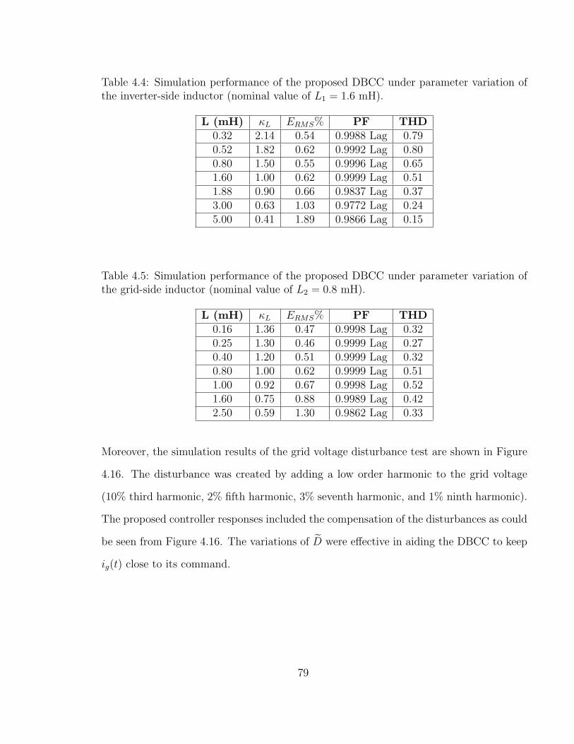
Table 4.4: Simulation performance of the proposed DBCC under parameter variation ofthe inverter-side inductor (nominal value of L1 = 1.6 mH).
L (mH) κL ERMS% PF THD0.32 2.14 0.54 0.9988 Lag 0.790.52 1.82 0.62 0.9992 Lag 0.800.80 1.50 0.55 0.9996 Lag 0.651.60 1.00 0.62 0.9999 Lag 0.511.88 0.90 0.66 0.9837 Lag 0.373.00 0.63 1.03 0.9772 Lag 0.245.00 0.41 1.89 0.9866 Lag 0.15
Table 4.5: Simulation performance of the proposed DBCC under parameter variation ofthe grid-side inductor (nominal value of L2 = 0.8 mH).
L (mH) κL ERMS% PF THD0.16 1.36 0.47 0.9998 Lag 0.320.25 1.30 0.46 0.9999 Lag 0.270.40 1.20 0.51 0.9999 Lag 0.320.80 1.00 0.62 0.9999 Lag 0.511.00 0.92 0.67 0.9998 Lag 0.521.60 0.75 0.88 0.9989 Lag 0.422.50 0.59 1.30 0.9862 Lag 0.33
Moreover, the simulation results of the grid voltage disturbance test are shown in Figure
4.16. The disturbance was created by adding a low order harmonic to the grid voltage
(10% third harmonic, 2% fifth harmonic, 3% seventh harmonic, and 1% ninth harmonic).
The proposed controller responses included the compensation of the disturbances as could
be seen from Figure 4.16. The variations of D were effective in aiding the DBCC to keep
ig(t) close to its command.
79
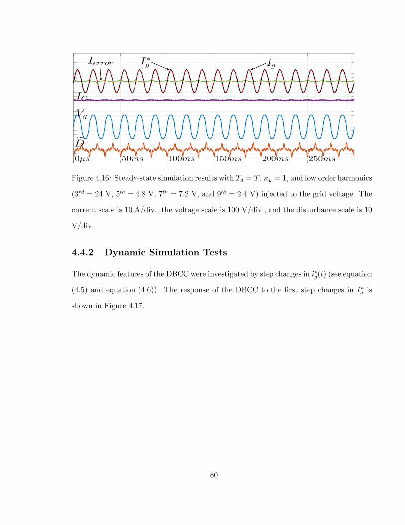
0µs 50ms 100ms 150ms 200ms 250ms
D
Vg
IC
Ierror I∗g Ig
Figure 4.16: Steady-state simulation results with Td = T , κL = 1, and low order harmonics
(3rd = 24 V, 5th = 4.8 V, 7th = 7.2 V, and 9th = 2.4 V) injected to the grid voltage. The
current scale is 10 A/div., the voltage scale is 100 V/div., and the disturbance scale is 10
V/div.
4.4.2 Dynamic Simulation Tests
The dynamic features of the DBCC were investigated by step changes in i∗g(t) (see equation
(4.5) and equation (4.6)). The response of the DBCC to the first step changes in I∗g is
shown in Figure 4.17.
80

0µs 50ms 100ms 150ms 200ms 250ms
D
IerrorIg
I∗gI∗g Ierror
Ig
Figure 4.17: Dynamic simulation results to step up/down (0 A to 40 A) with Td = T
and κL = 1. The current scale is 10 A/div., the disturbance scale is 20 V/div., and the
zoomed-in time scale is 2 msec./div.
Figure 4.18 shows the response to the second step changes in I∗g . It can be seen from
Figure 4.17 and Figure 4.18 that the DBCC was able to accurately respond to the step
changes in the command current with settling time close to 10 msec.
0µs 50ms 100ms 150ms 200ms 250ms
D
IerrorI∗g
Ig
I∗g
IerrorIg
Figure 4.18: Dynamic simulation results to step up/down (20 A to 40 A) with Td = T
and κL = 1. The current scale is 10 A/div., the disturbance scale is 20 V/div., and the
zoomed-in time scale is 2 msec./div.
81

4.5 Performance Comparison With Other Con-
trollers
In order to compare the performance of the DBCC and demonstrate its advantages,
similar simulation tests were carried out for other controllers. The predictive controller
with delay compensator [84] (PCDC) and traditional predictive controller [85] (TPC)
were used in these tests. The block diagrams of both controllers are given in Appendix
B. Table 4.6 summarizes the performance comparisons of these controllers for operating a
1φ VS dc-ac PEC, with L-type filter and Td = 0.5T . The steady-state performances were
compared using the ERMS, phase error, and stability range. The DBCC had shown greater
stability range with respect to variation in system parameters. In addition, the dynamic
performances were compared using the response times and overshoot percentages. The
DBCC showed faster responses to step changes in the command current.
Table 4.6: Simulation Results Comparison.
Evaluation Index DBCC PCDC TPCRobustness Range κL < 7 κL < 2 κL < 2ERMS at κL = 1 0.67% 0.66% 0.93%
Phase Error (degrees) 2.0o 2.3o 2.6o
Response Time (msec) 0.7 0.8 0.9Overshoot during step up 5.8% 4.0% 5.4%
Overshoot during step down 90% 30% 50%
Figure 4.19 shows the performance of these controllers with respect to changes in κL
(parameter variation). It can be seen from Figure 4.19 that the DBCC was capable of
maintaining low ERMS with negligible sensitivity to κL. These results also show that the
PCDC was able to maintain a low ERMS for 0.5 < κL ≤ 1.5, while the TPC was able
to maintain a low ERMS for 0.5 < κL ≤ 1. The large tracking errors of the PCDC and
TPC for high values of κL were due to operating these controller outside their robustness
82

regions.
Model Mismatch (κL)0 1 2 3 4 5 6 7
ERM
S%
0
5
10
15
DBCCPCDC
TPC
Figure 4.19: Simulation steady-state error comparison of the 1φ dc-ac PEC, with L-type
filter, when controlled by the proposed dead-beat current controller (DBCC), predictive
controller with delay compensator (PCDC), and traditional predictive controller (TPC)
with respect to the model mismatch ratio κL.
4.6 Summary
This chapter has presented and discussed performance features of the DBCC that has
been developed for 1φ VS dc-ac PECs. The presented performance features have been
obtained through simulation tests under different operating and loading conditions. Sim-
ulation tests have been conducted using a model that has been constructed using MAT-
LAB/SIMULINK software. In all tests, two cases have been simulated to demonstrate the
responses of the proposed controller during steady-state and dynamic conditions. On one
hand, steady-state tests have been set to investigate the ability of the DBCC to operate
the 1φ VS dc-ac PEC so that the injected current closely follows its command. Steady-
state tests have been carried out for different values of L, as well as grid-side harmonic
83

distortions. On the other hand, dynamic tests have been set to investigate the ability of
the DBCC to stably operate the 1φ VS dc-ac PEC under step changes in the command
current (or command power injection to the host grid), and ensure the grid injected to
the grid closely follows its command. Dynamic tests have been carried out for different
levels of step changes in the command current. In all tests, the DBCC has been found
capable of accurately responding to changes loading levels and/or changes in system pa-
rameters. Observed performance features of the DBCC have been further demonstrated
through comparisons with the predictive controller with delay compensator (PCDC) and
the traditional predictive controller (TPC). These comparisons have confirmed that the
proposed controller can offer a better performance under parameter variations, a wider
range of stability, and a faster response to the changes in loading levels. Finally, ob-
tained performance features through simulation tests will be confirmed and supported by
experimental tests as detailed in the next chapter.
84
Chapter 5
Performance Evaluation:
Experimental Tests
5.1 Overview
Chapter 4 has presented and discussed preliminary performance testing for the dead-beat
current controller, when operates an interconnected single-phase voltage-source H-bridge
dc-ac power electronic converter. The proposed controller have demonstrated remarkable
capabilities for operating the dc-ac PEC to deliver power to the host grid. These per-
formance features have been tested under various steady-state and dynamic conditions,
along with different deviations in system parameters and grid-side voltages. In all tests,
the DBCC has shown its abilities to maintain the operation of the 1φ VS dc-ac PEC in a
close track with its command. Observed performance features through simulation tests re-
quire additional verifications to complete the characterization of the DBCC performance.
In this chapter, the experimental tests for the DBCC are presented and discussed. The
desired experimental tests are carried out for a 10 kW interconnected system. The test
system is composed from three main parts which are an uncontrolled rectifier, a dc-dc
85
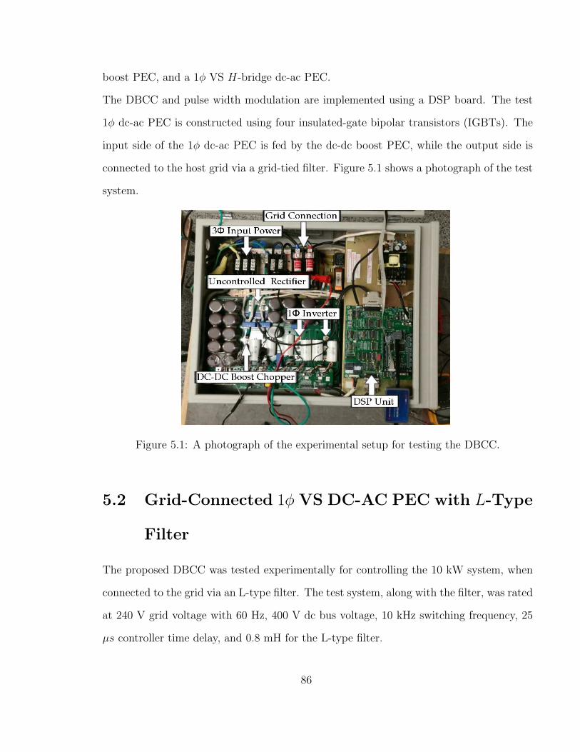
boost PEC, and a 1φ VS H-bridge dc-ac PEC.
The DBCC and pulse width modulation are implemented using a DSP board. The test
1φ dc-ac PEC is constructed using four insulated-gate bipolar transistors (IGBTs). The
input side of the 1φ dc-ac PEC is fed by the dc-dc boost PEC, while the output side is
connected to the host grid via a grid-tied filter. Figure 5.1 shows a photograph of the test
system.
Figure 5.1: A photograph of the experimental setup for testing the DBCC.
5.2 Grid-Connected 1φ VS DC-AC PEC with L-Type
Filter
The proposed DBCC was tested experimentally for controlling the 10 kW system, when
connected to the grid via an L-type filter. The test system, along with the filter, was rated
at 240 V grid voltage with 60 Hz, 400 V dc bus voltage, 10 kHz switching frequency, 25
µs controller time delay, and 0.8 mH for the L-type filter.
86

Several tests were conducted to evaluate the performance of the proposed DBCC. The
following test cases present and discuss some of the obtained test results. In all tested
cases, the reference current i∗g(t) was determined using the command powers P ∗g and Q∗
g
as:
i∗g(t) =√2
(P ∗g
Vg(rms)
)sin (2πfgt− θi∗) (5.1)
where Vg is the grid voltage, fg is the nominal frequency of the host grid, and θi∗ is the
phase of i∗g(t), which is determined as:
θi∗ = tan−1
(Q∗
g
P ∗g
)(5.2)
5.2.1 Steady-State Experimental Test
In this test, the 10 kW system was operated for several values of power delivery to the
grid, ranging from P ∗g = 2.4 kW to 9.6 kW and Q∗
g = 0. These values of P ∗g were translated
into the command current I∗g(rms) as:
10 A ≤ I∗g(rms) ≤ 40 A; θi∗ = 0;
Figure 5.2 shows the grid current and voltage waveforms for P ∗g = 8.4 kW. Table 5.1
summarizes the steady-state performance for all tested cases. Experimental test results
demonstrate that the proposed DBCC was able to maintain ig(t) at its command value
with less than 0.5% ERMS. In addition, the delivered power had relativity high power
factor indicating a good tracking of i∗g(t) and a low THD value. The observed responses
of the developed controller demonstrated its ability to maintain the quantity and quality
of the injected power to the grid in the steady-state condition.
87
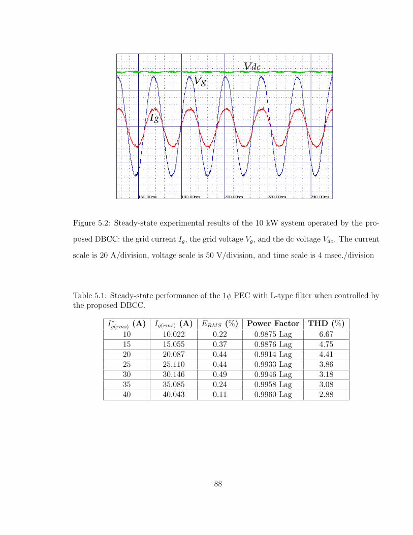
Figure 5.2: Steady-state experimental results of the 10 kW system operated by the pro-
posed DBCC: the grid current Ig, the grid voltage Vg, and the dc voltage Vdc. The current
scale is 20 A/division, voltage scale is 50 V/division, and time scale is 4 msec./division
Table 5.1: Steady-state performance of the 1φ PEC with L-type filter when controlled bythe proposed DBCC.
I∗g(rms) (A) Ig(rms) (A) ERMS (%) Power Factor THD (%)
10 10.022 0.22 0.9875 Lag 6.6715 15.055 0.37 0.9876 Lag 4.7520 20.087 0.44 0.9914 Lag 4.4125 25.110 0.44 0.9933 Lag 3.8630 30.146 0.49 0.9946 Lag 3.1835 35.085 0.24 0.9958 Lag 3.0840 40.043 0.11 0.9960 Lag 2.88
88
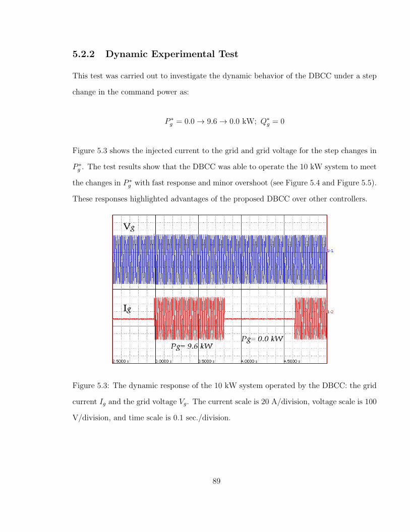
5.2.2 Dynamic Experimental Test
This test was carried out to investigate the dynamic behavior of the DBCC under a step
change in the command power as:
P ∗g = 0.0 → 9.6 → 0.0 kW; Q∗
g = 0
Figure 5.3 shows the injected current to the grid and grid voltage for the step changes in
P ∗g . The test results show that the DBCC was able to operate the 10 kW system to meet
the changes in P ∗g with fast response and minor overshoot (see Figure 5.4 and Figure 5.5).
These responses highlighted advantages of the proposed DBCC over other controllers.
Figure 5.3: The dynamic response of the 10 kW system operated by the DBCC: the grid
current Ig and the grid voltage Vg. The current scale is 20 A/division, voltage scale is 100
V/division, and time scale is 0.1 sec./division.
89
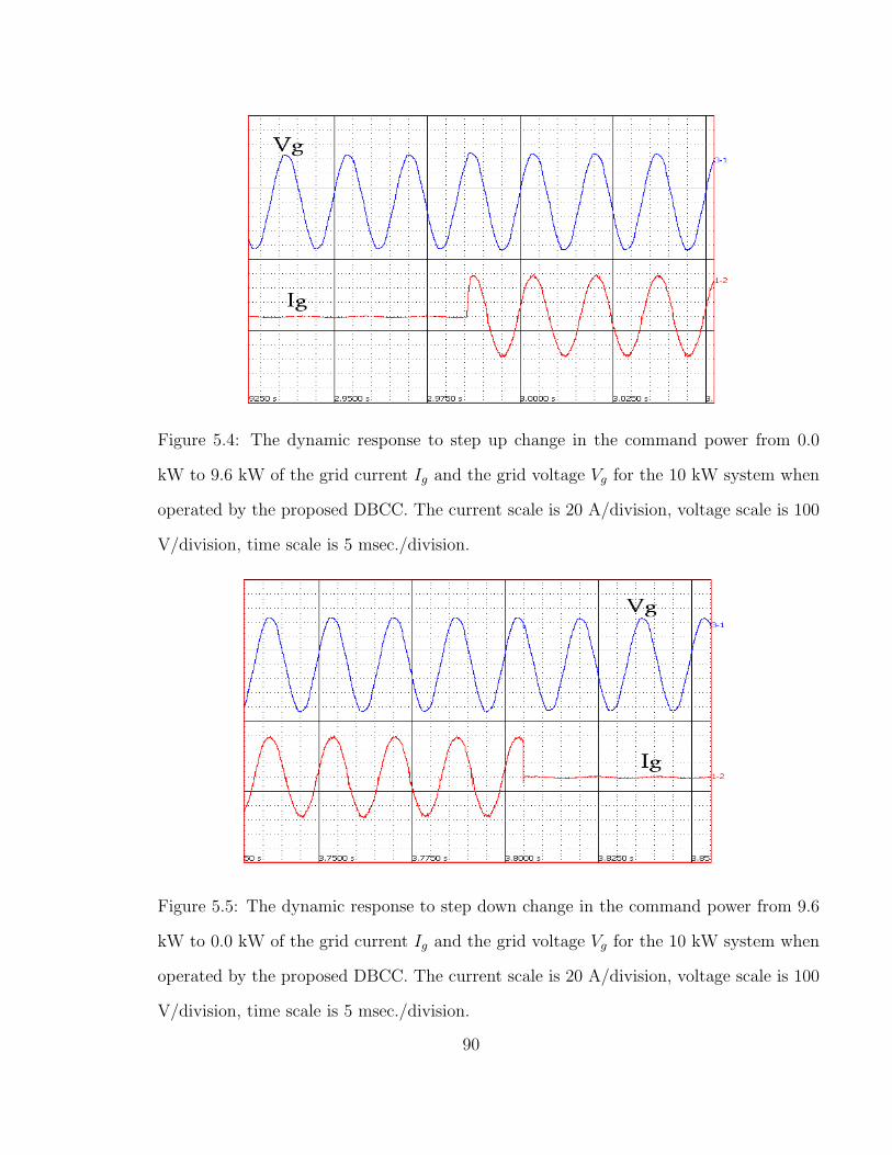
Figure 5.4: The dynamic response to step up change in the command power from 0.0
kW to 9.6 kW of the grid current Ig and the grid voltage Vg for the 10 kW system when
operated by the proposed DBCC. The current scale is 20 A/division, voltage scale is 100
V/division, time scale is 5 msec./division.
Figure 5.5: The dynamic response to step down change in the command power from 9.6
kW to 0.0 kW of the grid current Ig and the grid voltage Vg for the 10 kW system when
operated by the proposed DBCC. The current scale is 20 A/division, voltage scale is 100
V/division, time scale is 5 msec./division.
90
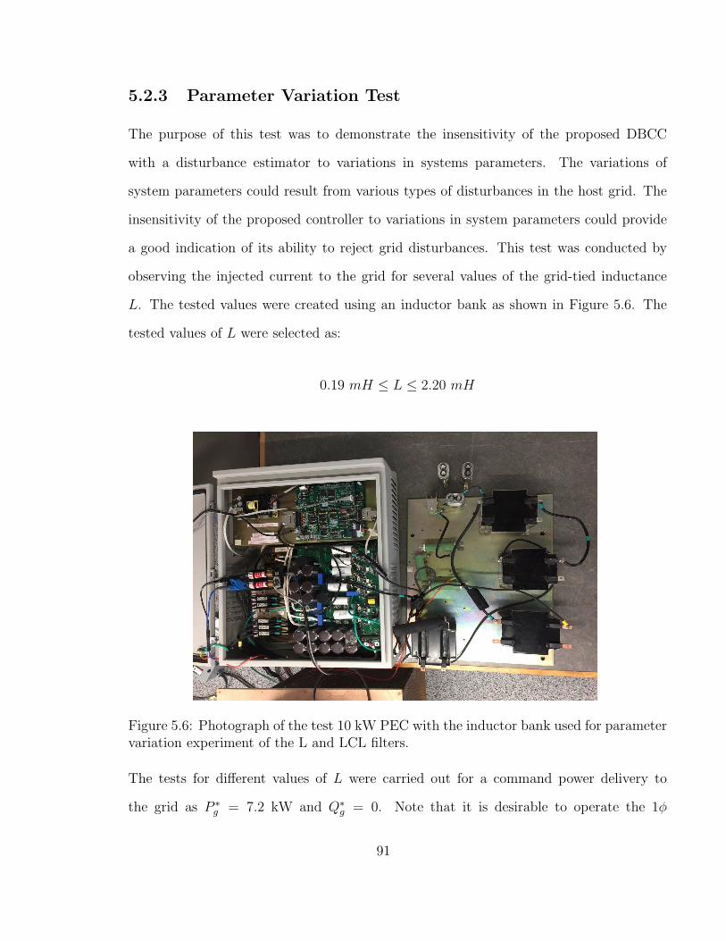
5.2.3 Parameter Variation Test
The purpose of this test was to demonstrate the insensitivity of the proposed DBCC
with a disturbance estimator to variations in systems parameters. The variations of
system parameters could result from various types of disturbances in the host grid. The
insensitivity of the proposed controller to variations in system parameters could provide
a good indication of its ability to reject grid disturbances. This test was conducted by
observing the injected current to the grid for several values of the grid-tied inductance
L. The tested values were created using an inductor bank as shown in Figure 5.6. The
tested values of L were selected as:
0.19 mH ≤ L ≤ 2.20 mH
Figure 5.6: Photograph of the test 10 kW PEC with the inductor bank used for parametervariation experiment of the L and LCL filters.
The tests for different values of L were carried out for a command power delivery to
the grid as P ∗g = 7.2 kW and Q∗
g = 0. Note that it is desirable to operate the 1φ
91
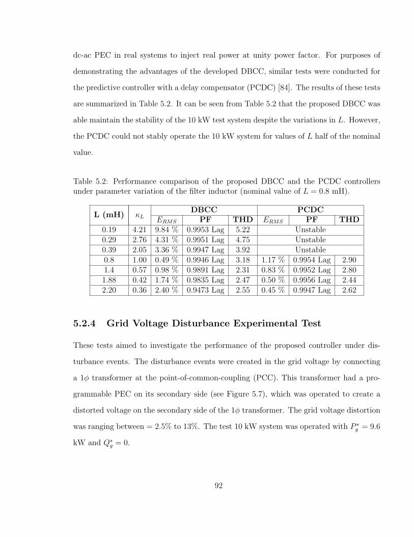
dc-ac PEC in real systems to inject real power at unity power factor. For purposes of
demonstrating the advantages of the developed DBCC, similar tests were conducted for
the predictive controller with a delay compensator (PCDC) [84]. The results of these tests
are summarized in Table 5.2. It can be seen from Table 5.2 that the proposed DBCC was
able maintain the stability of the 10 kW test system despite the variations in L. However,
the PCDC could not stably operate the 10 kW system for values of L half of the nominal
value.
Table 5.2: Performance comparison of the proposed DBCC and the PCDC controllersunder parameter variation of the filter inductor (nominal value of L = 0.8 mH).
L (mH) κLDBCC PCDC
ERMS PF THD ERMS PF THD0.19 4.21 9.84 % 0.9953 Lag 5.22 Unstable0.29 2.76 4.31 % 0.9951 Lag 4.75 Unstable0.39 2.05 3.36 % 0.9947 Lag 3.92 Unstable0.8 1.00 0.49 % 0.9946 Lag 3.18 1.17 % 0.9954 Lag 2.901.4 0.57 0.98 % 0.9891 Lag 2.31 0.83 % 0.9952 Lag 2.801.88 0.42 1.74 % 0.9835 Lag 2.47 0.50 % 0.9956 Lag 2.442.20 0.36 2.40 % 0.9473 Lag 2.55 0.45 % 0.9947 Lag 2.62
5.2.4 Grid Voltage Disturbance Experimental Test
These tests aimed to investigate the performance of the proposed controller under dis-
turbance events. The disturbance events were created in the grid voltage by connecting
a 1φ transformer at the point-of-common-coupling (PCC). This transformer had a pro-
grammable PEC on its secondary side (see Figure 5.7), which was operated to create a
distorted voltage on the secondary side of the 1φ transformer. The grid voltage distortion
was ranging between = 2.5% to 13%. The test 10 kW system was operated with P ∗g = 9.6
kW and Q∗g = 0.
92

Figure 5.7: Grid voltage disturbance experiment setup.
Figure 5.8 shows the injected current to the grid Ig and the grid voltage Vg for this
test with 12.22% distortion in the grid voltage. It can be seen from Figure 5.8 that the
proposed DBCC was able to operate the test system to inject a high quality current Ig
despite the distortion in the grid voltage Vg.
93

Figure 5.8: Experimental results of the 10 kW system operated by the DBCC: the grid
voltage Vg and the grid current Ig under grid voltage disturbance. The current scale is 20
A/division, voltage scale is 100 V/division, and time scale is 4 msec./division.
For this case, the harmonic components of Vg and Ig were obtained using the HIOKI
PW3198 Power Quality Analyzer (see Figure 5.9 and Figure 5.10). In these tests, the pro-
posed DBCC was able to reject the low order harmonics (3rd, 5th, and 7th) presented in the
grid voltage and to maintain ig(t) at its command with ERMS=2.32% and THD=2.67%.
94

Figure 5.9: Screen shot of the THD measurements for the grid voltage Vg captured from
HIOKI PW3198 Power Quality Analyzer.
Figure 5.10: Screen shot of the THD measurements for the grid current Ig captured from
HIOKI PW3198 Power Quality Analyzer.
Figure 5.11 illustrates all the recorded measurements and their interpolation curve for
these tests. It can be observed from Figure 5.11 that the proposed DBCC maintained
the THD of the injected current ig(t) below 3.5% regardless of the distortion in the grid
voltage.
95
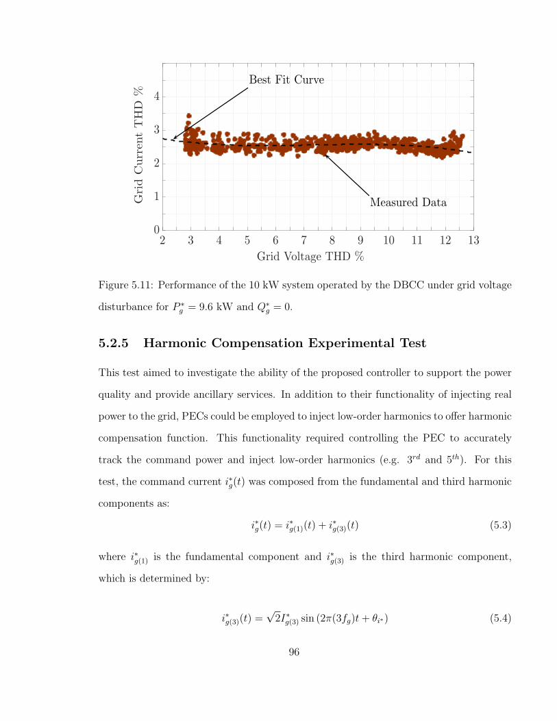
Grid Voltage THD %
2 3 4 5 6 7 8 9 10 11 12 13
GridCurrentTHD
%
0
1
2
3
4
Measured Data
Best Fit Curve
Figure 5.11: Performance of the 10 kW system operated by the DBCC under grid voltage
disturbance for P ∗g = 9.6 kW and Q∗
g = 0.
5.2.5 Harmonic Compensation Experimental Test
This test aimed to investigate the ability of the proposed controller to support the power
quality and provide ancillary services. In addition to their functionality of injecting real
power to the grid, PECs could be employed to inject low-order harmonics to offer harmonic
compensation function. This functionality required controlling the PEC to accurately
track the command power and inject low-order harmonics (e.g. 3rd and 5th). For this
test, the command current i∗g(t) was composed from the fundamental and third harmonic
components as:
i∗g(t) = i∗g(1)(t) + i∗g(3)(t) (5.3)
where i∗g(1) is the fundamental component and i∗g(3) is the third harmonic component,
which is determined by:
i∗g(3)(t) =√2I∗g(3) sin (2π(3fg)t+ θi∗) (5.4)
96
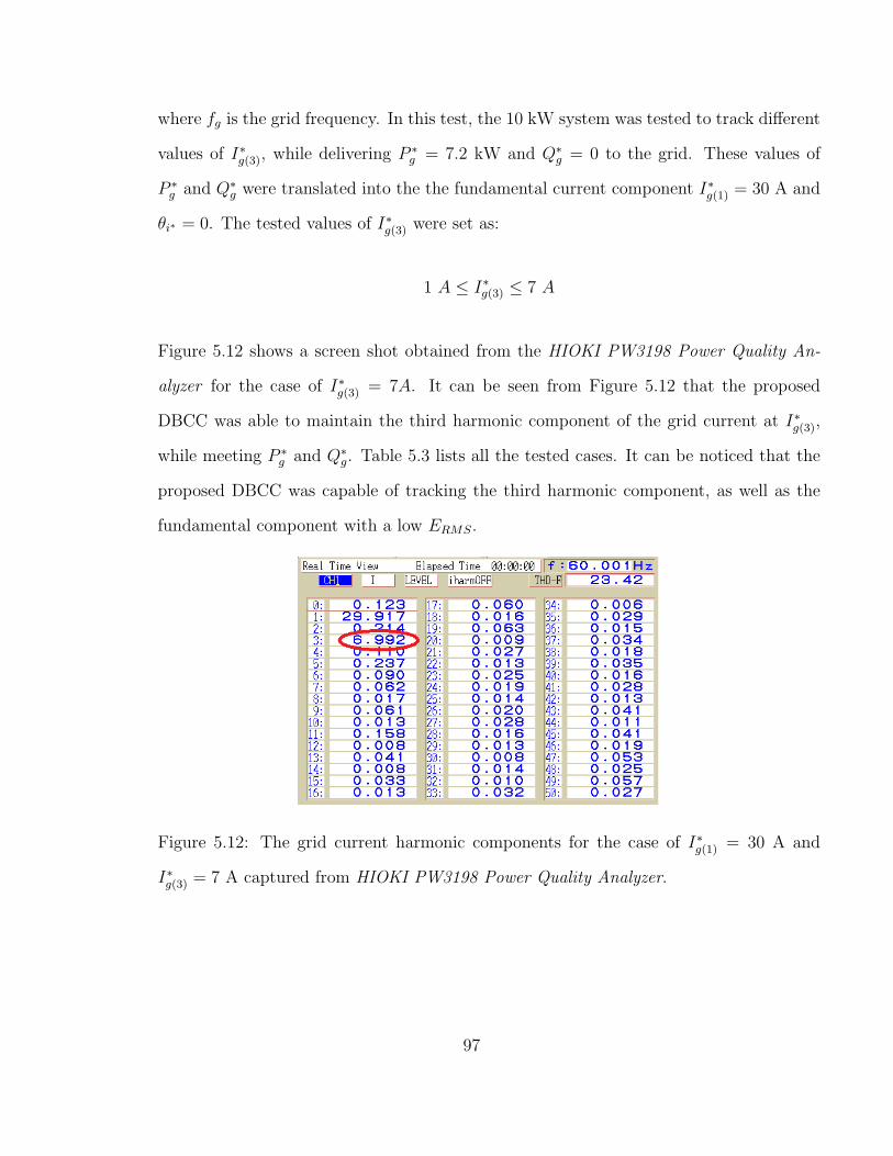
where fg is the grid frequency. In this test, the 10 kW system was tested to track different
values of I∗g(3), while delivering P ∗g = 7.2 kW and Q∗
g = 0 to the grid. These values of
P ∗g and Q∗
g were translated into the the fundamental current component I∗g(1) = 30 A and
θi∗ = 0. The tested values of I∗g(3) were set as:
1 A ≤ I∗g(3) ≤ 7 A
Figure 5.12 shows a screen shot obtained from the HIOKI PW3198 Power Quality An-
alyzer for the case of I∗g(3) = 7A. It can be seen from Figure 5.12 that the proposed
DBCC was able to maintain the third harmonic component of the grid current at I∗g(3),
while meeting P ∗g and Q∗
g. Table 5.3 lists all the tested cases. It can be noticed that the
proposed DBCC was capable of tracking the third harmonic component, as well as the
fundamental component with a low ERMS.
Figure 5.12: The grid current harmonic components for the case of I∗g(1) = 30 A and
I∗g(3) = 7 A captured from HIOKI PW3198 Power Quality Analyzer.
97

Table 5.3: Performance of the DBCC tracking the third harmonic current component.
I∗g(3) Ig(3) ERMS (%) Ig(1)1 1.050 5.00 30.1512 1.989 0.55 30.0043 2.988 0.40 29.9944 3.985 0.38 29.9015 4.983 0.34 29.9166 5.952 0.80 29.9067 6.992 0.11 29.917
Similar to the third harmonic case, the proposed DBCC was also tested for tracking the
fifth harmonic component. For this test, the command current i∗g(t) was composed from
the fundamental and fifth harmonic components as:
i∗g(t) = i∗g(1)(t) + i∗g(5)(t) (5.5)
where i∗g(5)(t) is the desired fifth harmonic current component, which is determined by:
i∗g(5)(t) =√2I∗g(5) sin (2π(5fg)t+ θi∗) (5.6)
The tested values of I∗g(5) were set as:
1 A ≤ I∗g(5) ≤ 7 A
Figure 5.13 shows a screen shot obtained from the HIOKI PW3198 Power Quality Ana-
lyzer for the case of tracking I∗g(5) = 5 A. Table 5.4 lists all the tested cases. It can be
seen that the proposed controller was able to track the fifth harmonic current component
with a good accuracy.
98
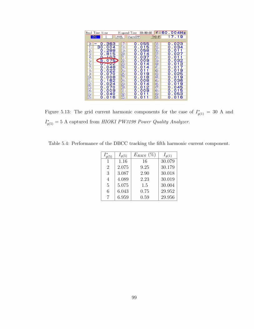
Figure 5.13: The grid current harmonic components for the case of I∗g(1) = 30 A and
I∗g(5) = 5 A captured from HIOKI PW3198 Power Quality Analyzer.
Table 5.4: Performance of the DBCC tracking the fifth harmonic current component.
I∗g(5) Ig(5) ERMS (%) Ig(1)1 1.16 16 30.0792 2.075 9.25 30.1793 3.087 2.90 30.0184 4.089 2.23 30.0195 5.075 1.5 30.0046 6.043 0.75 29.9527 6.959 0.59 29.956
99
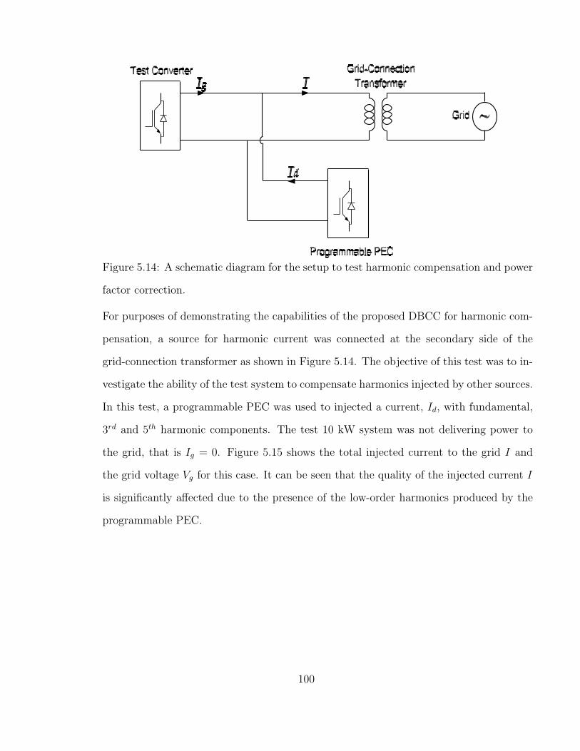
Figure 5.14: A schematic diagram for the setup to test harmonic compensation and power
factor correction.
For purposes of demonstrating the capabilities of the proposed DBCC for harmonic com-
pensation, a source for harmonic current was connected at the secondary side of the
grid-connection transformer as shown in Figure 5.14. The objective of this test was to in-
vestigate the ability of the test system to compensate harmonics injected by other sources.
In this test, a programmable PEC was used to injected a current, Id, with fundamental,
3rd and 5th harmonic components. The test 10 kW system was not delivering power to
the grid, that is Ig = 0. Figure 5.15 shows the total injected current to the grid I and
the grid voltage Vg for this case. It can be seen that the quality of the injected current I
is significantly affected due to the presence of the low-order harmonics produced by the
programmable PEC.
100

Figure 5.15: The waveforms of the injected current I and the grid voltage Vg without
harmonic compensation. The current scale is 15 A/division, voltage scale is 50 V/division,
and time scale is 5 msec./division.
In order to improve the quality of the injected current I, the test PEC was used to
compensate for the harmonic components. Figure 5.16 shows the waveforms of the in-
jected current I and grid voltage Vg with the harmonic compensation. One can see from
Figure 5.16 that the low-order harmonics of the current I were significantly reduced, as
demonstrated by the data in Table 5.6.
101

Figure 5.16: The waveforms of the injected current I and the grid voltage Vg with harmonic
compensation. The current scale is 15 A/division, voltage scale is 50 V/division, and time
scale is 5 msec./division.
Table 5.5: Harmonic components of the total current I before and after the compensation.
Harmonics Without compensation With compensation3rd 4 A 0.45 A5th 1 A 0.46 A
5.2.6 Power Factor Correction Experimental Test
In this test, the ability of the developed controller to provide power factor correction was
investigated. The correction of the power factor could be achieved by injecting or drawing
certain amount of reactive power. This objective could be accomplished by operating the
test system to follow a command power factor PF ∗. In such applications, the grid voltage
could be used as the reference (i.e. θv = 0). The required grid current angle could be
102
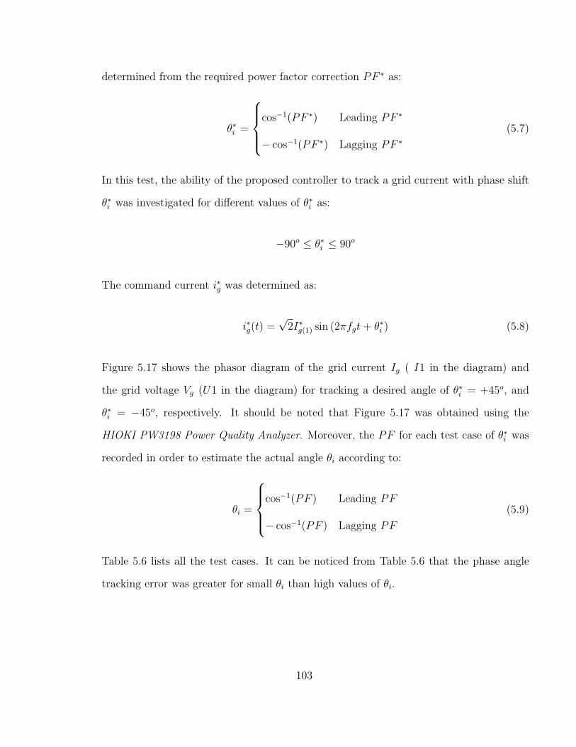
determined from the required power factor correction PF ∗ as:
θ∗i =
cos−1(PF ∗) Leading PF ∗
− cos−1(PF ∗) Lagging PF ∗
(5.7)
In this test, the ability of the proposed controller to track a grid current with phase shift
θ∗i was investigated for different values of θ∗i as:
−90o ≤ θ∗i ≤ 90o
The command current i∗g was determined as:
i∗g(t) =√2I∗g(1) sin (2πfgt+ θ∗i ) (5.8)
Figure 5.17 shows the phasor diagram of the grid current Ig ( I1 in the diagram) and
the grid voltage Vg (U1 in the diagram) for tracking a desired angle of θ∗i = +45o, and
θ∗i = −45o, respectively. It should be noted that Figure 5.17 was obtained using the
HIOKI PW3198 Power Quality Analyzer. Moreover, the PF for each test case of θ∗i was
recorded in order to estimate the actual angle θi according to:
θi =
cos−1(PF ) Leading PF
− cos−1(PF ) Lagging PF
(5.9)
Table 5.6 lists all the test cases. It can be noticed from Table 5.6 that the phase angle
tracking error was greater for small θi than high values of θi.
103

Figure 5.17: Phasor diagram of the grid current (I1) and grid voltage (U1) for (a) θ∗i =
+45o and (b) θ∗i = −45o.
Table 5.6: Performance the proposed DBCC in tracking the grid current with phase shiftθ∗.
Command Values Measured Values Errorθ∗i PF ∗ θi PF θerror % PFerror %
−90o 0 −88.99o 0.0176 Lag 1.12 −−75o 0.2588 Lag −75.56o 0.2494 Lag 0.75 3.63−60o 0.5000 Lag −60.74o 0.4887 Lag 1.23 2.26−45o 0.7071 Lag −45.65o 0.6991 Lag 1.4 1.13−30o 0.8660 Lag −30.66o 0.8602 Lag 2.2 0.67−15o 0.9659 Lag −15.93o 0.9616 Lag 6.2 0.460o 1 −4.93o 0.9963 Lag − 0.37
+15o 0.9659 Lead +15.74o 0.9625 Lead 4.90 0.35+30o 0.8660 Lead +30.27o 0.8637 Lead 0.90 0.27+45o 0.7071 Lead +45.25o 0.7040 Lead 0.56 0.42+60o 0.5000 Lead +60.36o 0.4945 Lead 0.60 1.10+75o 0.2588 Lead +75.30o 0.2537 Lead 0.40 1.97+90o 0 +89.64o 0.0062 Lead 0.40 −
In order to demonstrate the capabilities of the proposed DBCC in operating the 10 kW
system with a power factor correction functionality, an experiment was conducted based
on the set-up shown in Figure 5.14. In this experiment, a programmable PEC was used
104

to inject 2.4 kW into the grid with a power factor of 0.97. The resulting phasor diagram
of the total current injected to the grid I and the grid voltage Vg is shown in Figure 5.18
(a). In this initial stage of this test, the 10 kW system was not delivering power to the
grid (Ig = 0). It can be seen from Figure 5.18 (a) that the angle between the grid voltage
and grid current was not zero (θ ≈ +14o). In order to compensate the power factor and
correct the angle θ, the test system was operated to inject current Ig with θ∗i = −14o.
Figure 5.18 (b) shows the phasor diagram of the total current I and the grid voltage Vg
after correcting the angle θ. It can be seen that the angle with the power factor correction
was minimized (θ ≈ 0) and the power factor was corrected to be PF ≈1.
Figure 5.18: Phasor diagram of the total grid current (I = I1) and grid voltage (Vg = U1)
(a) without power factor compensation and (b) with power factor compensation.
5.3 Grid-Connected 1φ VS DC-AC PEC with LCL-
Type Filter
The proposed DBCC was experimentally tested for controlling the 10 kW system con-
nected to the grid via an LCL-type filter. The test setup for these tests was specified with
240 V grid voltage with 60 Hz, 400 V dc bus voltage, 10 kHz switching frequency, 50 µs
105
controller time delay, 1.6 mH inverter-side inductor, 0.8 mH grid-side inductor, 10 µF
filter capacitor, and 2.4 Ω damping resistor.
5.3.1 Steady-State Experimental Test
The steady-state performance of the 10 kW system was investigated for different loading
conditions, ranging from P ∗g = 2.4 kW to 8.4 kW and Q∗
g = 0. These values were
translated into the command current I∗g(rms) as:
10 A ≤ I∗g(rms) ≤ 35 A; θi∗ = 0;
Figure 5.20 shows the grid current and voltage waveforms for P ∗g = 7.2 kW. A summary
for the results obtained for all values of P ∗g is provided in Table 5.7. It can be seen from
Table 5.7 that the proposed controller was able to maintain Ig at its command value with
0.5% ERMS. Furthermore, the power factor was relativity high and THD was low for all
the tested cases. The results in Table 5.1 and Table 5.7 indicated that the tested system
performance was relativity similar under the L-type and LCL-type filters. Although the
LCL-type filter could offer better disturbance rejection capabilities, the employment of
the disturbance estimator in the proposed DBCC made the performance of the tested
system independent of the filter type used.
106

Figure 5.19: The experimental results of the developed current controller: the injected
current into the grid Ig, and grid voltage Vg. The current scale is 50 A/division, voltage
scale is 200 V/division, and time scale is 5 µsec/division.
Table 5.7: Steady-state performance of the 1φ VS dc-ac PEC with LCL-type filter whencontrolled by the proposed DBCC.
I∗g (A) Ig (A) ERMS (%) Power Factor THD (%)
10 10.033 0.33 0.9967 Lag 5.5515 15.053 0.35 0.9978 Lag 3.7620 19.910 0.45 0.9977 Lag 3.1325 24.876 0.50 0.9972 Lag 3.1730 30.100 0.33 0.9973 Lag 3.2235 34.888 0.32 0.9968 Lag 3.45
107

5.3.2 Dynamic Experimental Test
The objective of this test was to investigate the dynamic responses of the DBCC during
step changes in the power delivered to the grid. Two sets of step changes in P ∗g were
created to investigate the ability of the proposed DBCC to respond to large or small
changes in P ∗g . The first step change was created as:
P ∗g = 0.0 → 2.4 kW; Q∗
g = 0
Figure 5.20 shows the injected current to the grid and grid voltage for the first step change
in P ∗g .
Figure 5.20: The injected current into the grid Ig, and grid voltage Vg under a step
change in the command power P ∗g . The current scale is 50 A/division, voltage scale is 200
V/division, and time scale is 25 µsec/division for the upper window and 5 µsec/division
for the lower window.
108
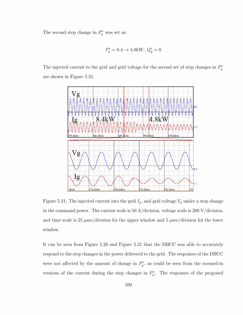
The second step change in P ∗g was set as:
P ∗g = 8.4 → 4.8kW; Q∗
g = 0
The injected current to the grid and grid voltage for the second set of step changes in P ∗g
are shown in Figure 5.21.
Figure 5.21: The injected current into the grid Ig, and grid voltage Vg under a step change
in the command power. The current scale is 50 A/division, voltage scale is 200 V/division,
and time scale is 25 µsec/division for the upper window and 5 µsec/division for the lower
window.
It can be seen from Figure 5.20 and Figure 5.21 that the DBCC was able to accurately
respond to the step changes in the power delivered to the grid. The responses of the DBCC
were not affected by the amount of change in P ∗g , as could be seen from the zoomed-in
versions of the current during the step changes in P ∗g . The responses of the proposed
109

controller changed Ig with short transient during the increase and decrease of P ∗g . The
results of this test revealed good dynamic features of the DBCC without sensitivity to
the amount of change in P ∗g .
5.3.3 Parameter Variation Experimental Test
The objective of this test was to demonstrate the ability of the DBCC to reject distur-
bances from the grid-side, as well as to demonstrate its insensitivity to changes in systems
parameters. This test was conducted by observing the injected current to the grid for
several values the inverter-side inductor L1 and the grid-side inductor L2. The tested
values of L1 and L2 of the LCL filter were varied using an inductor bank similar to that
shown in Figure 5.6. The tested values of L1 were selected as:
0.32 mH ≤ L1 ≤ 5 mH
This test was carried out for a command power delivery to the grid as P ∗g = 7.2 kW and
Q∗g = 0. Table 5.8 lists the testing results for the different variations in L1. It can be seen
from the test results that the DBCC was able to operate the 10 kW system in the range
of 0.32 mH ≤ L1 ≤ 5 mH with great accuracy, high power factor and low THD.
Table 5.8: Performance of the PEC under parameter variation of the inverter-side inductor(nominal value of L1 = 1.6 mH).
L1 (mH) κL Ig (A) ERMS (%) PF THD (%)0.32 2.14 30.094 0.35 0.9970 Lag 3.550.52 1.82 29.896 0.35 0.9970 Lag 3.400.8 1.50 29.893 0.36 0.9970 Lag 3.391.6 1.00 30.100 0.33 0.9973 Lag 3.221.88 0.90 29.802 0.66 0.9960 Lag 3.663 0.63 29.551 1.50 0.9905 Lag 4.835 0.41 29.364 2.12 0.9880 Lag 5.06
110
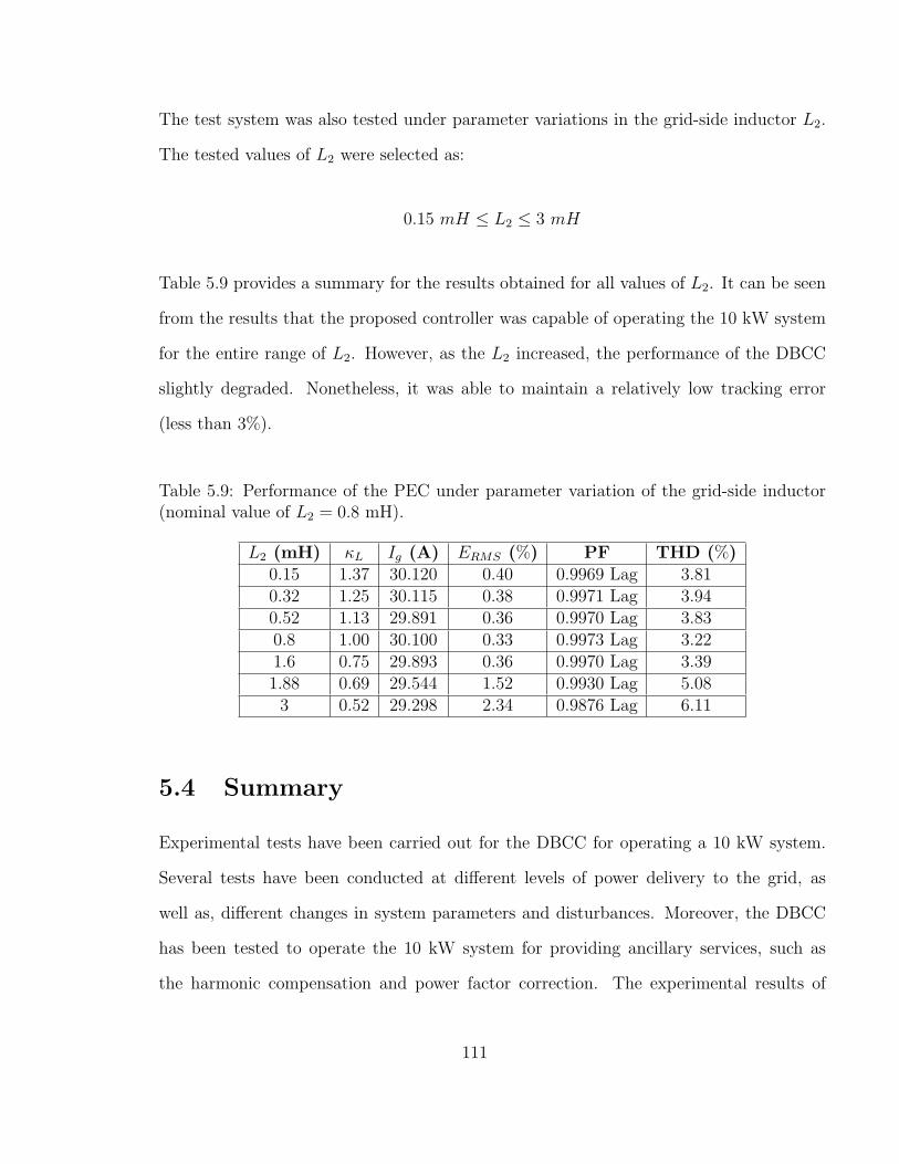
The test system was also tested under parameter variations in the grid-side inductor L2.
The tested values of L2 were selected as:
0.15 mH ≤ L2 ≤ 3 mH
Table 5.9 provides a summary for the results obtained for all values of L2. It can be seen
from the results that the proposed controller was capable of operating the 10 kW system
for the entire range of L2. However, as the L2 increased, the performance of the DBCC
slightly degraded. Nonetheless, it was able to maintain a relatively low tracking error
(less than 3%).
Table 5.9: Performance of the PEC under parameter variation of the grid-side inductor(nominal value of L2 = 0.8 mH).
L2 (mH) κL Ig (A) ERMS (%) PF THD (%)0.15 1.37 30.120 0.40 0.9969 Lag 3.810.32 1.25 30.115 0.38 0.9971 Lag 3.940.52 1.13 29.891 0.36 0.9970 Lag 3.830.8 1.00 30.100 0.33 0.9973 Lag 3.221.6 0.75 29.893 0.36 0.9970 Lag 3.391.88 0.69 29.544 1.52 0.9930 Lag 5.083 0.52 29.298 2.34 0.9876 Lag 6.11
5.4 Summary
Experimental tests have been carried out for the DBCC for operating a 10 kW system.
Several tests have been conducted at different levels of power delivery to the grid, as
well as, different changes in system parameters and disturbances. Moreover, the DBCC
has been tested to operate the 10 kW system for providing ancillary services, such as
the harmonic compensation and power factor correction. The experimental results of
111

the proposed controller have demonstrated accurate and fast responses. These response
features have been achieved by including a disturbance estimator, which has facilitated
initiating the controller actions with negligible sensitivity to system parameters and other
disturbances.
Observed performance features have been further highlighted by comparisons with other
controllers under similar operating conditions. Results of performance comparisons have
shown that the DBCC can maintain its performance features without being impacted by
the changes of the power delivered to the grid. Table 5.10 highlights the performance com-
parison between the DBCC, proportional-integral (PI) [16,18–21], proportional-resonance
(PR) [29,31–47], and predictive controller with delay compensator (PCDC) [84].
Table 5.10: Performance comparison of current controller of grid-connected 1φ VS dc-acPEC.
Criteria DBCC PI [16,18–21] PR [29,31–47] PCDC [84]Steady-State
Low High Zero LowErrorPower
High Poor High HighQualityTransient
Fast Slow Slow FastResponseParameter
Negligible Sensitive Sensitive SensitiveVariation
DisturbanceGreat Poor Great Great
Rejection
112
Chapter 6
Conclusions and Future Work
6.1 Summary
Energy conversion systems, which are fed by renewable sources, are widely utilized to
meet the growing demands for electric energy. These systems have demonstrated the
ability to be interconnected to a host power system, or to be operated in a stand-alone
mode for supplying isolated loads. In each configuration, energy conversion systems are
mostly designed to deliver their electric energy through power electronic converters. The
interconnection of PECs into power systems have raised several concerns due to possi-
ble impacts on the operation, control, and dynamic or transient conditions on the host
power systems. Among these concerns is the harmonic distortion that is caused by in-
terconnected PECs during steady-state or dynamic conditions. Various standards and
industrial codes have been developed to address and set limits for levels of harmonic dis-
tortion due to interconnected PECs. One of the widely accepted approach to meet these
standards and codes is the employment of current controllers to operate interconnected
PECs.
This thesis research has developed new current controllers for 1φ voltage-source H-bridge
113

dc-ac PECs that are interconnected to a power system. The proposed current controllers
are designed as dead-beat controllers that are featured with observers and disturbance
estimators. The design of DBCCs, observers, and estimators has been carried out using
the pole-placement method, when the controlled 1φ VS dc-ac PEC is grid-connected via
L-type and LCL-type filters. The performance of the DBCCs, with their observers and
disturbance estimators, has been evaluated through simulation and experimental tests for
various steady-state and dynamic conditions. Test results have shown that the proposed
current controllers are capable of reducing the harmonic distortion on the grid-side, closely
following command active and reactive powers delivered to the host grid, maintaining
stability under variations in system parameters, and following their command powers
during grid-side disturbances. Observed performance features have been supported by
comparisons with other current controllers under similar operating conditions.
6.2 Conclusions
The design, analysis, and performance of the DBCCs, with observers and disturbance
estimators, have been investigated in this thesis. The focus has been on interconnected
1φ voltage-source H-bridge dc-ac PECs, which are widely used in grid-connected photo-
voltaic, wind energy, and battery storage systems. The research conducted and presented
in this thesis can lead to the following conclusions:
• The developed DBCCs can provide accurate, stable, and fast responses with low
steady-state errors and high power quality.
• The proposed controllers can operate grid-connected 1φ VS dc-ac PECs with minor
sensitivity to different types of disturbances and deviations in measured quantities.
• The DBCCs can offer fast, accurate, and stable responses to changes in the power
114

delivered to the grid, and/or changes in system parameters.
• The DBCCs can maintain their performance features over a wide range of power
delivery and power factor values.
• The DBCCs can be used for operating the grid-connected 1φ VS dc-ac to support
the power quality and provide harmonic compensation and power factor correction
functions.
• The developed current controllers can reject grid-side disturbances, regardless of the
type or design of the grid-tied filter.
6.3 Contributions
The research work presented in this thesis has achieved several contributions to improve
the operation and functionality of grid-connected 1φ VS dc-ac PECs. These contributions
can be summarized as:
• A family of dead-beat current controllers have been presented and implemented for
grid-connected 1φ VS dc-ac PECs:
– Dead-beat controller with first-order observer for gird-tied L filters.
– Dead-beat controller with third-order observer for grid-tied LCL filters.
The dead-beat current controllers are commonly used for operating 1φ VS dc-ac
PECs with first order gird-tied L filter. In this thesis, the performance of the
dead-beat current controllers has been improved and their sensitivity to parameter
variation is reduced using observers and estimators. Moreover, the dead-beat cur-
rent controllers have been extended to operate 1φ VS dc-ac PECs with third-order
grid-tied LCL filters without the need for additional sensors or measurements. In
115

addition, the control scheme can be extended to higher-order filters with proper ob-
server design. Unlike traditional observers, where observed states converge to actual
states, the proposed observers have been designed such that observed and actual
states converge only when estimators accurately track the disturbances on the sys-
tem. In addition, exiting estimators require the knowledge of system parameters
and time delay values during their design. These requirements can cause existing
estimators to be sensitive to parameter variation. Moreover, a precise time delay is
difficult to obtain due to its dependence on the digital implementation platform. In
this thesis, disturbance estimators have been designed to be independent of system
parameters, as well as time delay values.
• Experiments on the grid-connected 1φ VS dc-ac PEC have verified the developed
controllers and their performance. The steady-state performance has been verified
by testing the dc-ac PEC under different loading conditions. The developed con-
trollers have been found to be able to regulate the power delivery to the grid with
low relative error, high power factor and low total harmonic distortion. The dy-
namic performance has been also tested under step changes in the command power.
The results have shown that the developed controllers are capable of meeting the
changes of command power with fast response and minor overshoot. In addition,
the effect of the system parameters variation on the performance of the developed
controllers have been tested by observing the injected current to the grid for several
values of the grid-tied inductance. The developed controllers are found capable of
maintaining the stability of the 1φ VS dc-ac PEC despite the variations in the filter
inductance. In addition, the performance of the proposed controllers has been tested
under distorted grid voltage, i.e. harmonic distortion. The grid-connected 1φ VS
dc-ac PEC operated by the developed dead-beat current controllers is found capable
116

of rejecting grid-side disturbances. The ability of the proposed controllers to inject
low-order harmonics for harmonic compensation function has been also tested. It is
found that the developed controllers are able to maintain the third and the fifth har-
monic components of the grid current at their command values. Furthermore, the
capability of the proposed controllers to provide power factor correction has been
verified by operating the dc-ac PEC to inject/draw certain amount of reactive power
to/from the host grid. The performance of the proposed controllers has been found
independent of the type of the grid-tied filter, grid-side disturbances, levels of power
delivery to the grid, and power factor at the PCC. These features of the developed
dead-beat current controllers can offer robust solutions to the stability challenges in
predictive current controllers, slow responses in proportional resonance controllers,
and limited disturbance rejection capabilities in proportional-integral controllers.
• A comprehensive analysis has been conducted for the stability of the developed
family of dead-beat current controllers, when operating grid-connected 1φ VS dc-ac
PEC. In this analysis, the effects of parameter variations and digital implementation
requirements, have been investigated. Furthermore, the stability analysis has been
conducted such that it can be employed for the reliable design of any DBCC to
operate a grid-connected 1φ VS dc-ac PEC. Finally, a detailed steady-state analysis
has been carried out to investigate the effect of different grid-side disturbances on the
operation of grid-connected 1φ VS dc-ac PECs, when controlled by the developed
family of DBCCs.
6.4 Future Works
The research work presented in this thesis can provide avenues for future research works
including:
117

• The adoption of the proposed controller for other grid-connected 1φ PECs, such as
1φ ac-dc PECs.
• The implementation of the developed DBCC for smart inverters that are deployed
to improve power quality and provide various ancillary services.
• The extension of the proposed DBCC to operate 3φ PECs that are operated in
grid-connection mode.
• The employment of the developed observer and disturbance estimator in other con-
trollers including PR controllers.
• The investigation of the applicability of the developed DBCC for 1φ bi-directional
grid-connected PECs.
118

Bibliography
[1] R. Beres, W. Wang, M. Liserre, F. Blaabjerg, and C. Bak, “A Review of Passive Power
Filters for Three-Phase Grid-Connected Voltage-Source Converters,” IEEE Journal of
Emerging and Selected Topics in Power Electronics, Vol. 4, No. 1, pp. 54–69, 2016.
[2] J. C. Das, “Passive filtersPotentialities and limitations,” IEEE Trans. Ind. Appl.,
Vol. 40, No. 1, pp. 232–241, 2004.
[3] A. A. Rockhill, M. Liserre, R. Teodorescu, and P. Rodriguez, “Grid-filter design for a
multimegawatt medium-voltage voltage-source inverter,” IEEE Trans. Ind. Electron.,
Vol. 58, No. 4, pp. 1205–1217, 2011.
[4] J. Muhlethaler, M. Schweizer, R. Blattmann, J. W. Kolar, and A. Ecklebe, “Optimal
design of LCL harmonic filters for three-phase PFC rectifiers,” IEEE Trans. Power
Electron., Vol. 28, No. 7, pp. 3114–3125, 2013.
[5] M. Liserre, F. Blaabjerg, and S. Hansen, “Design and control of an LCL-filter-based
three-phase active rectifier,” IEEE Trans. Ind. Appl., Vol. 41, No. 5, pp. 1281–1291,
2005.
[6] K. Jalili and S. Bernet, “Design of LCL filters of active-front-end two-level voltage-
source converters,” IEEE Trans. Ind. Electron., Vol. 56, No. 5, pp. 1674–1689, 2009.
119
[7] A. Reznik, M. G. Simoes, A. Al-Durra, and S. M. Muyeen, “LCL filter design and per-
formance analysis for grid-interconnected systems,” IEEE Trans. Ind. Appl., Vol. 50,
No. 2, pp. 1225–1232, 2014.
[8] Y. Jiao and F. C. Lee, “LCL filter design and inductor current ripple analysis for a
three-level NPC grid interface converter,” IEEE Trans. Power Electron, Vol. 30, No. 9,
pp. 4659–4668, 2015.
[9] B. Bolsens, K. De Brabandere, J. Van den Keybus, J. Driesen, and R. Belmans,
“Model-based generation of low distortion currents in grid coupled PWM-inverters
using an LCL output filter,” IEEE Trans. Power Electron, Vol. 21, No. 4, pp. 1032–
1040, 2006.
[10] W. Wu, Y. He and F. Blaabjerg, “An LLCL Power Filter for Single-Phase Grid-Tied
Inverter,” IEEE Transactions on Power Electronics, Vol. 27, No. 2, pp. 782–789, Feb.
2012.
[11] X. Zhang, H. Zhu, F. Li, F. Liu, C. Liu and B. Li, “An LCL-LC power filter for grid-
tied inverter,” 2013 IEEE International Conference of IEEE Region 10 (TENCON
2013), Xi’an, 2013, pp. 1-4.
[12] Z. Liu, H. Wu, Y. Liu, J. Ji, W. Wu and F. Blaabjerg, “Modelling of the modified-
LLCL-filter-based single-phase grid-tied Aalborg inverter,” IET Power Electronics,
Vol. 10, No. 2, pp. 151–155, Feb. 2017.
[13] IEEE Application Guide for IEEE Standard for Interconnecting Distributed Re-
sources With Electric Power Systems, IEEE Std. 1547.2-2008, 2008.
120

[14] A. I. Maswood and F. Liu, “Combining the Wind Power Generation System With
Energy Storage Equipment,” IEEE Trans. on Industry Applications, Vol. 43, No. 2,
pp. 593–599, 2007.
[15] J. A. Suul, K. Ljokelsoy, T. Midtsund, and T. Undeland, “Synchronous Reference
Frame Hysteresis Current Control for Grid Converter Applications,” IEEE Trans. on
Industry Applications, Vol. 47, No. 5, pp. 2183–2194, 2007.
[16] O. Aguilar, R. Tapia, A. Valderrabano and H. Minor, “Design and Performance Com-
parison of PI and Adaptive Current Controllers for a WECS,” IEEE Latin America
Transactions, Vol. 13, No. 5, pp. 1361–1368, 2015.
[17] C. R. Baier et al, “Analysis and Design of a Control Strategy for Tracking Sinu-
soidal References in Single-Phase Grid-Connected Current-Source Inverters,” IEEE
Transactions on Power Electronics, Vol. 33, No. 1, pp. 819–832, 2018.
[18] D. N. Zmood, D. G. Holmes and G. H. Bode, “Frequency-domain analysis of three-
phase linear current regulators,” IEEE Trans. on Industry Applications, Vol. 37, No. 2,
pp. 601–610, 2001.
[19] C. D. Schauder and S. A. Moarn,“Multiple reference frame controller for active filters
and power line conditioners,” U.S. Patent 5 309 353, May, 1994
[20] C. D. Schauder and R. Caddy,“Current Control of Voltage-Source Inverters for Fast
Four-Quadrant Drive Performance,” IEEE Trans. on Industry Applications, vol. IA-
18, no. 2, pp. 163–171, Mar. 1982.
[21] D. N. Zmood and D. G. Holmes,“Stationary frame current regulation of PWM invert-
ers with zero steady-state error,” IEEE Trans. on Power Electronics, vol. 18, no. 3,
pp. 814–822, May 2003.
121

[22] M. A. Hannan, Z. A. Ghani, A. Mohamed, and M. N. Uddin, “Real-Time Testing of
a Fuzzy-Logic-Controller-Based Grid-Connected Photovoltaic Inverter System,” IEEE
Trans. on Industry Applications, Vol. 51, No. 6, pp. 4775–4784, 2015.
[23] C. W. Tao, C. M. Wang and C. W. Chang, “A Design of a DCAC Inverter Using a
Modified ZVS-PWM Auxiliary Commutation Pole and a DSP-Based PID-Like Fuzzy
Control,” IEEE Trans. on Industrial Electronics, Vol. 63, No. 1, pp. 397–405, 2016.
[24] B. Burton, F. Kamran, R. G. Harley, T. G. Habetler, M. A. Brooke, and R. Pod-
dar, “Identification and Control of Induction Motor Stator Currents Using Fast On-
Line Random Training of a Neural Network,” IEEE Trans. on Industry Applications,
Vol. 33, No. 3, pp. 697–704, 1997.
[25] B. Burton, R. G. Harley, G. Diana, and J. L. Rodgerson, “Implementation of a
Neural Network to Adaptively Identify and Control VSI-Fed Induction Motor Stator
Currents,” IEEE Trans. on Industry Applications, Vol. 34, No. 3, pp. 580–588, 1998.
[26] Mi-Ching Tsai and Wu-Sung Yao,“Design of a plug-in type repetitive controller
for periodic inputs,” in IEEE Trans. on Control Systems Technology, vol. 10, no. 4,
pp. 547–555, Jul 2002.
[27] R. Grino and R. Costa-Castello,“Digital repetitive plug-in controller for odd-
harmonic periodic references and disturbances,” Automatica, vol. 41, no. 1, pp. 153–
157, 2005.
[28] G. Pipeleers, B. Demeulenaere, J. D. Schutter and J. Swevers,“Generalised repetitive
control: relaxing the period-delay-based structure,” IET Control Theory & Applica-
tions, vol. 3, no. 11, pp. 1528–1536, November 2009.
122
[29] R. Teodorescu, F. Blaabjerg, M. Liserre and P. C. Loh, “Proportional-resonant con-
trollers and filters for grid-connected voltage-source converters,” IEEE Proceedings -
Electric Power Applications, Vol. 153, No. 5, pp. 750–762, 2006.
[30] I. Sefa, N. Altin, S. Ozdemir, O. Kaplan, “Fuzzy PI controlled inverter for grid inter-
active renewable energy systems,” IET Renewable Power Generation, Vol. 9, No. 7,
pp. 729–738, 2015.
[31] H. Komurcugil, N. Altin, S. Ozdemir and I. Sefa, “Lyapunov-Function and
Proportional-Resonant-Based Control Strategy for Single-Phase Grid-Connected VSI
With LCL Filter,” IEEE Trans. on Industrial Electronics, Vol. 63, No. 5, pp. 2838–
2849, 2016.
[32] B. Li, W. Yao, L. Hang and L. M. Tolbert, “Robust proportional resonant regulator
for grid-connected voltage source inverter (VSI) using direct pole placement design
method,” IET Power Electronics, Vol. 5, No. 8, pp. 1367–1373, 2012.
[33] T. Hornik and Q. C. Zhong, “A Current-Control Strategy for Voltage-Source In-
verters in Microgrids Based on H∞ and Repetitive Control,” IEEE Trans. on Power
Electronics, Vol. 26, No. 3, pp. 943–952, 2011.
[34] M. Liserre, R. Teodorescu and F. Blaabjerg,“Stability of photovoltaic and wind tur-
bine grid-connected inverters for a large set of grid impedance values,” IEEE Trans.
on Power Electronics, vol. 21, no. 1, pp. 263–273, Jan 2006.
[35] J. Hu, Y. He, L. Xu and B. W. Williams,“Improved Control of DFIG Systems Dur-
ing Network Unbalance Using PIR Current Regulators,” IEEE Trans. on Industrial
Electronics, vol. 56, no. 2, pp. 439–451, Feb 2009.
123
[36] P. Zhou, Y. He and D. Sun,“Improved Direct Power Control of a DFIG-Based Wind
Turbine During Network Unbalance,” IEEE Trans. on Power Electronics, vol. 24,
no. 11, pp. 2465–2474, Nov 2009.
[37] G. K. Andersen, K. B. Larsen, F. B. Bendixen,“Variable speed wind turbine, a
resonant control system, a method of operating a variable speed wind turbine, use
of a resonant control system and use of a method in a variable speed wind turbine,”
US 7902686 B2, March 2011.
[38] V. Phan and H. Lee,“Enhanced Proportional-Resonant Current Controller for Un-
balanced Stand-alone DFIG-based Wind Turbines,” Journal of Electrical Engineering
and Technology, vol. 5, no. 3, pp. 443–450, Sept 2010.
[39] V. Phan and H. Lee,“An Improved Control Strategy Using a PI-Resonant Controller
for an Unbalanced Stand-Alone Doubly-Fed Induction Generator,” Journal of power
electronics, vol. 10, no. 2, pp. 194–202, March 2010.
[40] R. Teodorescu, F. Blaabjerg, U. Borup and M. Liserre,“A new control structure for
grid-connected LCL PV inverters with zero steady-state error and selective harmonic
compensation,” Applied Power Electronics Conference and Exposition, vol. 1, pp. 580–
586, 2004.
[41] M. Castilla, J. Miret, J. Matas, L. Garcia de Vicuna and J. M. Guerrero,“Linear
Current Control Scheme With Series Resonant Harmonic Compensator for Single-
Phase Grid-Connected Photovoltaic Inverters,” IEEE Trans. on Industrial Electronics,
vol. 55, no. 7, pp. 2724–2733, July 2008.
[42] M. Castilla, J. Miret, J. Matas, L. Garcia de Vicuna and J. M. Guerrero,“Control De-
sign Guidelines for Single-Phase Grid-Connected Photovoltaic Inverters With Damped
124

Resonant Harmonic Compensators,” IEEE Trans. on Industrial Electronics, vol. 56,
no. 11, pp. 4492–4501, Nov 2009.
[43] X. Yuan, W. Merk, H. Stemmler and J. Allmeling,“Stationary-frame generalized
integrators for current control of active power filters with zero steady-state error for
current harmonics of concern under unbalanced and distorted operating conditions,”
IEEE Trans. on Industry Applications, vol. 38, no. 2, pp. 523–532, Mar/Apr 2002.
[44] C. Lascu, L. Asiminoaei, I. Boldea and F. Blaabjerg,“High Performance Current Con-
troller for Selective Harmonic Compensation in Active Power Filters,” IEEE Trans.
on Power Electronics, vol. 22, no. 5, pp. 1826–1835, Sept 2007.
[45] R. Bojoi, L. R. Limongi, D. Roiu and A. Tenconi,“Frequency-domain analysis of res-
onant current controllers for active power conditioners,” 2008 34th Annual Conference
of IEEE Industrial Electronics, Orlando, FL, 2008, pp. 3141–3148.
[46] F. D. Freijedo et al,“Frequency tracking of digital resonant filters for control of power
converters connected to public distribution systems,” IET Power Electronics, vol. 4,
no. 4, pp. 454–462, April 2011.
[47] A. Timbus, M. Liserre, R. Teodorescu, P. Rodriguez and F. Blaabjerg,“Evaluation
of Current Controllers for Distributed Power Generation Systems,” IEEE Trans. on
Power Electronics, vol. 24, no. 3, pp. 654–664, March 2009.
[48] S. Buso, S. Fasolo, and P. Mattavelli, “Uninterruptible Power Supply Multi-Loop
Control Employing Digital Predictive Voltage and Current Regulators,” IEEE Trans.
on Industry Applications, Vol. 37, No. 6, pp. 1846–1854, 2001.
125

[49] G. H. Bode, P. C. Loh, M. J. Newman, and D. G. Holmes, “An Improved Robust
Predictive Current Regulation Algorithm,” IEEE Trans. on Industry Applications,
Vol. 41, No. 6, pp. 1720–1733, 2005.
[50] D. Martin and E. Santi, “Autotuning of Digital Deadbeat Current Controllers for
Grid-Tie Inverters Using Wide Bandwidth Impedance Identification,” IEEE Trans.
on Industry Applications, Vol. 50, No. 1, pp. 441–451, 2014.
[51] R. Mikail, I. Husain, Y. Sozer, M. S. Islam, and T. Sebastian, “A Fixed Switching
Frequency Predictive Current Control Method for Switched Reluctance Machines,”
IEEE Trans. on Industry Applications, Vol. 50, No. 6, pp. 3717–3726, 2014.
[52] K. J. Lee, B. G. Park, R. Y. Kim, and D. S. Hyun, “Robust Predictive Current Con-
troller Based on a Disturbance Estimator in a Three Phase Grid-Connected Inverter,”
IEEE Trans. on Power Electronics, Vol. 27, No. 1, pp. 276–283, 2012.
[53] U. Abronzini, C. Attaianese, M. D. Arpino, M. D. Monaco, and G. Tomasso, “Steady-
State Dead-Time Compensation in VSI,” IEEE Trans. on Industrial Electronics,
Vol. 63, No. 9, pp. 5858–5866, 2016.
[54] J. Hu, J. Zhu, and D. G. Dorrell, “Model Predictive Control of Grid-Connected
Inverters for PV Systems with Flexible Power Regulation and Switching Frequency
Reduction,” IEEE Trans. on Industry Applications, Vol. 51, No. 1, pp. 587–594, 2015.
[55] P. Mattavelli, “An Improved Deadbeat Control for UPS Using Disturbance Ob-
servers,” IEEE Trans. on Industrial Electronics, Vol. 52, No. 1, pp. 206–212, 2005.
[56] Y. A. I. Mohamed and E. F. El-Saadany, “An Improved Deadbeat Current Con-
trol Scheme with a Novel Adaptive Self-tuning Load Model for a Three-Phase PWM
126

Voltage-Source Inverter,” IEEE Trans. on Industrial Electronics, Vol. 54, No. 2,
pp. 747–759, 2007.
[57] Q. Zeng and L. Chang, “An Advanced SVPWM-Based Predictive Current Controller
for Three-Phase Inverters in Distributed Generation Systems,” IEEE Trans. on In-
dustrial Electronics, Vol. 55, No. 3, pp. 1235–1246, 2008.
[58] S. Buso, T. Caldognetto, and D. I. Brandao, “Dead-Beat Current Controller for
Voltage-Source Converters with Improved Large-Signal Response,” IEEE Trans. on
Industry Applications, Vol. 52, No. 2, pp. 1588–1596, 2016.
[59] J. R. Fischer, S. A. Gonzlez, M. A. Herrn, M. G. Judewicz and D. O. Carrica,
“Calculation-Delay Tolerant Predictive Current Controller for Three-Phase Inverters,”
IEEE Trans. on Industrial Informatics, Vol. 10, No. 1, pp. 233–242, 2014.
[60] Y. A. R. I. Mohamed and E. F. El-Saadany,“Adaptive Discrete-Time Grid-Voltage
Sensorless Interfacing Scheme for Grid-Connected DG-Inverters Based on Neural-
Network Identification and Deadbeat Current Regulation,” IEEE Trans. on Power
Electronics, vol. 23, no. 1, pp. 308–321, Jan. 2008.
[61] J. M. Espi, J. Castello, R. Garca-Gil, G. Garcera and E. Figueres,“An Adaptive
Robust Predictive Current Control for Three-Phase Grid-Connected Inverters,” IEEE
Trans. on Industrial Electronics, vol. 58, no. 8, pp. 3537–3546, Aug. 2011.
[62] K. J. P. Macken, K. Vanthournout, J. Van den Keybus, G. Deconinck and R. J.
M. Belmans,“Distributed control of renewable generation units with integrated active
filter,” IEEE Trans. on Power Electronics, vol. 19, no. 5, pp. 1353–1360, Sept 2004.
127

[63] E. Wu and P. W. Lehn,“Digital Current Control of a Voltage Source Converter With
Active Damping of LCL Resonance,” IEEE Trans. on Power Electronics, vol. 21, no. 5,
pp. 1364–1373, Sept 2006.
[64] J. Mossoba and P. W. Lehn,“A controller architecture for high bandwidth active
power filters,” IEEE Trans. on Power Electronics, vol. 18, no. 1, pp. 317–325, Jan 2003.
[65] J. H. Allmeling,“A Control Structure for Fast Harmonics Compensation in Active
Filters,” IEEE Trans. on Power Electronics, vol. 19, no. 2, pp. 508–514, March 2004.
[66] T. Ahmed, K. Nishida, and M. Nakaoka,“A Novel Stand-Alone Induction Generator
System for AC and DC Power Applications,” IEEE Trans. on Industry Applications,
vol. 42, no. 4, pp. 934–945, July/August 2007.
[67] T. Ahmed, K. Nishida, and M. Nakaoka,“Advanced control for PWM converter and
variable-speed induction generator,” IET Electric Power Applications, vol. 1, no. 2,
pp. 239–247, March 2007.
[68] A. Yepes,“Digital Resonant Current Controllers For Voltage Source Converters,”
Ph.D. dissertation, Dept. Elect. Tech., University of Vigo, 2011.
[69] S. Buso and P. Mattavelli , Digital Control in Power Electronics, 2nd Ed. Morgan
and Claypool Publishers, 2006.
[70] R. Costa-Castello, R. Grino, R. Cardoner and E. Fossas,“High Performance Control
of a Single-Phase Shunt Active Filter,” IEEE Trans. on Control System Technology,
vol. 17, no. 6, pp. 1318–1329, Nov 2009.
[71] R. Costa-Castello, J. Nebot, and R. Grino,“Demonstration of the internal model
principle by digital repetitive control of an educational laboratory plant,” IEEE Trans.
on Education, vol. 48, no. 1, pp. 73–80, Feb 2005.
128
[72] R. Costa-Castello, R. Grino and E. Fossas,“Odd-harmonic digital repetitive control
of a single-phase current active filter,” IEEE Trans. on Power Electronics, vol. 19,
no. 4, pp. 1060–1068, July 2004.
[73] C. Kempf, W. C. Messner, M. Tomizuka and R. Horowitz,“Comparison of four
discrete-time repetitive control algorithms,” IEEE Control Systems Magazine, vol. 13,
no. 6, pp. 48–54, Dec 1993.
[74] Ying-Yu Tzou, Rong-Shyang Ou, Shih-Liang Jung and Meng-Yueh Chang,“High-
performance programmable AC power source with low harmonic distortion using DSP-
based repetitive control technique,” IEEE Trans. on Power Electronics, vol. 12, no. 4,
pp. 715–725, July 1997.
[75] B. A. Francis and W. M. Wonham,“The internal model principle for linear multivari-
able regulators,” Applied Mathematics and Optimization, vol. 2, no. 2, pp. 170–194,
Dec 1975.
[76] H. Cha, T. K. Vu and J. E. Kim,“Design and control of Proportional-Resonant con-
troller based Photovoltaic power conditioning system,” 2009 IEEE Energy Conversion
Congress and Exposition, San Jose, CA, 2009, pp. 2198–2205.
[77] Y. A. R. I. Mohamed and E. F. El-Saadany,“A Control Scheme for PWM Voltage-
Source Distributed-Generation Inverters for Fast Load-Voltage Regulation and Ef-
fective Mitigation of Unbalanced Voltage Disturbances,” IEEE Trans. on Industrial
Electronics, vol. 55, no. 5, pp. 2072–2084, May 2008.
[78] P. Mattavelli, G. Spiazzi and P. Tenti,“Predictive digital control of power factor
preregulators with input voltage estimation using disturbance observers,” IEEE Trans.
on Power Electronics, vol. 20, no. 1, pp. 140–147, Jan 2005.
129
[79] P. Mattavelli,“An improved deadbeat control for UPS using disturbance observers,”
IEEE Trans. on Industrial Electronics, vol. 52, no. 1, pp. 206–212, Feb 2005.
[80] Y. A. R. I. Mohamed and E. F. El-Saadany,“Robust High Bandwidth Discrete-Time
Predictive Current Control with Predictive Internal ModelA Unified Approach for
Voltage-Source PWM Converters,” IEEE Trans. on Power Electronics, vol. 23, no. 1,
pp. 126–136, Jan 2008.
[81] J. M. Espi Huerta, J. Castello, J. R. Fischer and R. Garcia-Gil,“A Synchronous Ref-
erence Frame Robust Predictive Current Control for Three-Phase Grid-Connected
Inverters,” IEEE Trans. on Industrial Electronics, vol. 57, no. 3, pp. 954–962,
March 2010.
[82] J. C. Moreno, J. M. Espi Huerta, R. G. Gil and S. A. Gonzalez,“A Robust Pre-
dictive Current Control for Three-Phase Grid-Connected Inverters,” IEEE Trans. on
Industrial Electronic, vol. 56, no. 6, pp. 1993–2004, June 2009.
[83] H. S. Kim and J. S. Ko,“Experimental position control of PMSM using disturbance
observer with system parameter compensator,” 2011 11th International Conference
on Control, Automation and Systems,Gyeonggi-do, 2011, pp. 1396–1401.
[84] R. Shao,“Power Converters for Residential PV and Hybrid Systems,” Ph.D. Disser-
tation, Dept. of Elect. and Comp. Eng., University of New Brunswick, 2010.
[85] O. Kukrer,“Discrete-time current control of voltage-fed three-phase PWM inverters,”
IEEE Trans. on Power Electronics, vol. 11, pp. 260–269, 1996.
[86] P. Cortes, M. P. Kazmierkowski, R. M. Kennel, D. E. Quevedo, and J. Ro-
driguez,“Predictive control in power electronics and drives,” IEEE Trans. on Industrial
Electronics, vol. 55, pp. 4312–4324, 2008.
130
[87] W. Wu and T. Tang,“Dual mode time-sharing cascaded sinusoidal inverter,” IEEE
Trans. on Energy Convers, vol. 22, no. 3, pp. 795–797, 2007.
[88] N. A. Ahmed, H. Woo Lee, and M. Nakaoka,“Dual-mode time-sharing sinewave-
modulation soft switching boost full-bridge one-stage power conditioner without elec-
trolytic capacitor DC link,” IEEE Trans. on Ind. Appl., vol. 43, no. 3, pp. 805–813,
2007.
[89] J. Shen, K. Rigbers, C. P. Dick, and R. W. De Doncker,“A dynamic boost converter
input stage for a double 120 flattop modulation based three phase inverter,” Proc.
IEEE Ind. Appl. Soc., pp. 1–7, 2008.
[90] J. C. Das, Power System Harmonics and Passive Filter Designs. Piscataway, NJ,
USA: Wiley, 2015.
[91] M. Liserre, A. DellAquila, and F. Blaabjerg,“Genetic algorithm-based design of the
active damping for an LCL-filter three-phase active rectifier, ” IEEE Trans. Power
Electron., vol. 19, no. 1, pp. 76–86, 2004.
[92] X. Wang, F. Blaabjerg, and P. C. Loh,“Grid-current-feedback active damping for
LCL resonance in grid-connected voltage-source converters, ” IEEE Trans. Power
Electron., vol. 31, no. 1, pp. 213–223, 2016.
[93] J. Arrillaga and N. R. Watson, Power System Harmonics. Chichester, U.K.: Wiley,
2003.
[94] R. N. Beres, X. Wang, F. Blaabjerg, M. Liserre, and C. L. Bak,“Optimal design
of high-order passive-damped filters for grid-connected applications,” IEEE Trans.
Power Electron., vol. 31, no. 4, pp. 2083–2098, 2016.
131
[95] W. Wu et al.,“A robust passive damping method for LLCL-filter-based grid-tied
inverters to minimize the effect of grid harmonic voltages,” IEEE Trans. Power Elec-
tron., vol. 29, no. 7, pp. 3279–3289, 2014.
[96] R. Pea-Alzola, M. Liserre, F. Blaabjerg, R. Sebastin, J. Dannehl, and F. W.
Fuchs,“Analysis of the passive damping losses in LCL-filter based grid converters,”
IEEE Trans. Power Electron., vol. 28, no. 6, pp. 2642–2646, 2013.
[97] N.Jaalam, N.A.Rahim, A.H.A.Bakar, C. Tan, A. Haidar,“A comprehensive review of
synchronization methods for grid-connected converters of renewable energy source,”
Renewable and Sustainable Energy Reviews., vol. 59, no. 1, pp. 1471–1481, 2016.
[98] Y. Tang, W. Yao, P. C. Loh and F. Blaabjerg,“Design of LCL Filters With LCL Res-
onance Frequencies Beyond the Nyquist Frequency for Grid-Connected Converters,”
IEEE Journal of Emerging and Selected Topics in Power Electronics., vol. 4, no. 1,
pp. 3–14, 2016.
132

Appendix A
The Disturbance Derivation of the Grid-Connected 1φ
AC-DC PECs with L Filter
Ig =Lm
Lz
−Td
T
z· I∗g +
TL(z
−Td
T − 1)
z − 1· Vg +
TLz
−Td
T
z − 1·∆Vg
(1)
Adding and subtracting the term I∗g · z−1 from equation (1) yields to:
Ig = I∗g · z−1 − I∗g · z−1 +Lm
Lz
−Td
T
z· I∗g +
TL(z
−Td
T − 1)
z − 1· Vg +
TLz
−Td
T
z − 1·∆Vg
(2)
Ig = I∗g · z−1 + I∗g · z−1(Lm
Lz
−Td
T − 1) +TL(z
−Td
T − 1)
z − 1· Vg +
TLz
−Td
T
z − 1·∆Vg
(3)
Ig = I∗g · z−1 +T
L
z−Td
T
z − 1(I∗g · z−1L
T
z − 1
z−Td
T
(L
Lm
z−Td
T − 1) + Vg
z−Td
T − 1
z−Td
T
+∆Vg) (4)
Equation (4) can be written as:
Ig = I∗g · z−1 +T
L
z−Td
T
z − 1·D (5)
where D is the the disturbance affecting the system, which is given by:
133

D = I∗g · z−1L
T
z − 1
z−Td
T
(L
Lm
z−Td
T − 1) + Vg
z−Td
T − 1
z−Td
T
+∆Vg (6)
Simplifying equation (6) yields to:
D = I∗g ·Lm
T
z − 1
z− I∗g ·
L
T
z − 1
z
1
z−Td
T
+ Vg ·z
−Td
T − 1
z−Td
T
+∆Vg (7)
Adding and subtracting the term I∗g · LT
z−1z
to equation (7):
D = I∗g ·Lm
T
z − 1
z+ I∗g ·
L
T
z − 1
z− I∗g
L
T
z − 1
z− I∗g ·
L
T
z − 1
z
1
z−Td
T
+ Vg ·z
−Td
T − 1
z−Td
T
+∆Vg
(8)
rearranging equation (8) yields to:
D = I∗g ·Lm − L
T
z − 1
z+ I∗g ·
L
T
z − 1
z(1− 1
z−Td
T
) + Vg · (1−1
z−Td
T
) + ∆Vg (9)
D = I∗g ·z − 1
z
(Lm − L)
T+
(I∗g ·
z − 1
z
L
T+ Vg
)(1− 1
z−Td
T
) + ∆Vg (10)
134

Continuous State Space Model Derivation of the Grid-
Connected 1φ AC-DC PECs with LCL Filter
Figure 1: A schematic diagram for grid-connected 1φ VS dc-ac PECs with LCL filter.
Figure 1 shows a schematic diagram of the grid-connected 1φ VS dc-ac PECs with LCL
filter. Using KVL, the following equation can be driven
−v0(t) + L1diodt
+ vc(t) = 0 (11)
Re-arranging equation (11) in term of the inverter current io(t) as:
L1diodt
=(v0(t)− vc(t)
)(12)
Similarly, using KVL, the following equation can be driven
−vc(t) + L2digdt
+ vg(t) = 0 (13)
135

Re-arranging equation (13) in term of the grid current ig(t) as:
L2digdt
=(vc(t)− vg(t)
)(14)
The capacitor voltage, vcap(t), is given by the following differential equation:
Cdvcapdt
=ic(t) (15)
Cdvcapdt
=io(t)− ig(t) (16)
The capacitor branch voltage, vc(t), is given by the addition of the capacitor voltage,
vcap(t), and the resistor voltage, vR(t). That is:
vc(t) =vcap(t) + vR(t) (17)
vc(t) =vcap(t) +R(ic(t)) (18)
vc(t) =vcap(t) +R(io(t)− ig(t)) (19)
Taking the derivative of equation (19) with respect to the time, t, yields to:
dvcdt
=dvcapdt
+R(diodt
− digdt
) (20)
Substituting equations (12), (14), and (16) in equation (20) as:
dvcdt
=1
C(io(t)− ig(t)) +
R
L1
(v0(t)− vc(t)
)− R
L2
(vc(t)− vg(t)
)(21)
Equation (21) can be simplified to:
dvcdt
=1
C
(i0(t)− ig(t)
)+
R
L1
v0(t) +R
L2
vg(t)−R(L1 + L2)
L1L2
vc(t) (22)
136
Equations (12), (14), and (22) represents the continuous state space model of the grid-
connected 1φ ac-dc PECs with LCL filter.
Differential Equation Derivation of the Grid-
Connected 1φ AC-DC PECs with LCL Filter
Re-arranging equation (12) in term of vc(t) as:
vc(t) = v0(t)− L1dio(t)
dt(23)
Substituting equation (23) in equation (14) yields to:
dig(t)
dt=
1
L2
(v0(t)− L1
dio(t)
dt− vg(t)
)(24)
The differential terms in (24) can be approximated using finite difference approximation
over the controller period, T , as:
di(t)
dt≈ ∆i(t)
∆t=
i(k + 1)− i(k)
T(25)
this approximation simplifies equation (24) to:
ig(k + 1)− ig(k)
T=
1
L2
(V0(t)− L1
io(k + 1)− io(k)
T− Vg(t)
)(26)
Where V0(k) and Vg(k) are the average output voltage and average grid voltage over T ,
respectively. Equation (26) cam be re-arranged to:
L2
T
(ig(k + 1)− ig(k)
)+
L1
T
(io(k + 1)− io(k)
)= V0(k)− Vg(k) (27)
137
It should be noted that the average output voltage is given by:
V0(k) = m(k)Vdc (28)
Where m(k) is the controller modulation index over T while Vdc is the dc voltage. The
current io(k + 1) can be expressed as:
io(k + 1) = ig(k + 1) + ic(k + 1) (29)
Where ic(k + 1) is the capacitor current at the future sample k + 1. Equation (27) can
be simplified using equations (28) and (29) as:
L1 + L2
Tig(k + 1)− L2
Tig(k)−
L1
Tio(k) +
L1
Tic(k + 1) = m(k)Vdc − Vg(k) (30)
Observed Grid and Inverter Currents Derivation of
the Grid-Connected 1φ AC-DC PECs with LCL Filter
The response of the observed grid current ig(k) can be driven by re-writing equation (30)
in term of the observed values as:
Lm1 + Lm2
Tig(k+1)−Lm2
Tig(k)−
Lm1
Tio(k)+
Lm1
Tic(k+1) = m(k)Vdc−Vg(k)−∆Vg(k) (31)
Where the control signal to the observer is given by:
m(k) =Lm1+Lm2
Ti∗g(k) +Kcx(k) + Vg(k) + ∆Vg(k)
Vdc
(32)
138
Note that the error in the grid voltage measurements, ∆Vg(k), appears in equations (31)
and (32) since the same measurement is used for both the observer and the controller.
Substituting equation (32) in equation (31) yields to:
Lm1 + Lm2
Tig(k + 1) +
Lm1
Tic(k + 1) =
Lm1 + Lm2
Ti∗g(k) (33)
Re-arranging equation (33) to:
ig(k + 1) = i∗g(k)−Lm1
Lm1 + Lm2
ic(k + 1) (34)
Equation (34) presents the observed grid current. To drive the equation of the observed
inverter current, the observed grid current can be expressed in term of the observed
inverter current and the observed capacitor current as:
ig(k + 1) = io(k + 1)− ic(k + 1) (35)
Substituting equation (35) into equation (34) yields to:
io(k + 1) = i∗g(k) +Lm2
Lm1 + Lm2
ic(k + 1) (36)
The Disturbance Derivation of the Grid-Connected 1φ
AC-DC PECs with LCL Filter
Equation (27) model the behavior of the grid-connected 1φ ac-dc PECs with LCL filter.
For the convenience of the reader, equation (27) is re-written below:
L2
T
(ig(k + 1)− ig(k)
)+
L1
T
(io(k + 1)− io(k)
)= V0(k)− Vg(k) (37)
139

Due to the time delay required by the controller, the average output voltage is given by
the previous value of the modulation index, that is:
V0(k) = m(k − 1)Vdc (38)
Where the modulation index is given by:
m(k − 1) =Lm1+Lm2
Ti∗g(k − 1) +Kcx(k − 1)− D(k − 1) + Vg(k − 1) + ∆Vg(k − 1)
Vdc
(39)
Substituting equations (38) and (39) in equation (37) yields to:
L2
T
(ig(k + 1)− ig(k)
)+
L1
T
(io(k + 1)− io(k)
)=
Lm1 + Lm2
Ti∗g(k − 1)
(40)
+Kcx(k − 1)− D(k − 1) + Vg(k − 1) + ∆Vg(k − 1)− Vg(k)
Note that the vector Kc and the observed values x(k) are given by:
Kc =
−Lm1
T
0
−Lm2
T
(41)
x(k) =
io(k)
vc(k)
ig(k)
(42)
140

Hence, equation (40) can be expressed as:
L2
T
(ig(k + 1)− ig(k)
)+
L1
T
(io(k + 1)− io(k)
)=
Lm1 + Lm2
Ti∗g(k − 1)
(43)
−Lm1
Tio(k − 1)− Lm2
Tig(k − 1)− D(k − 1) + Vg(k − 1) + ∆Vg(k − 1)− Vg(k)
The observer currents ig and io are given in equations (34) and (37), respectively. Sub-
stituting these equations in (43) yields to:
L2
T
(ig(k + 1)− ig(k)
)+
L1
T
(io(k + 1)− io(k)
)=
Lm1 + Lm2
Ti∗g(k − 1)
− Lm1
T(i∗g(k − 2) +
Lm2
Lm1 + Lm2
ic(k − 1))− Lm2
T(i∗g(k − 2)− Lm1
Lm1 + Lm2
ic(k − 1)) (44)
− D(k − 1) + Vg(k − 1) + ∆Vg(k − 1)− Vg(k)
Equation (44) can be simplified further to:
L2
T
(ig(k + 1)− ig(k)
)+
L1
T
(io(k + 1)− io(k)
)=
Lm1 + Lm2
Ti∗g(k − 1)
(45)
−Lm1 + Lm2
Ti∗g(k − 2)− D(k − 1) + Vg(k − 1) + ∆Vg(k − 1)− Vg(k)
141

The inverter current io can be expressed in term of the grid current ig and the capacitor
current ic. This substitution changes equation (45) to:
L2
T
(ig(k + 1)− ig(k)
)+
L1
T
(ig(k + 1) + ic(k + 1)− ig(k)− ic(k)
)=
Lm1 + Lm2
Ti∗g(k − 1)− Lm1 + Lm2
Ti∗g(k − 2)− D(k − 1) (46)
+ Vg(k − 1) + ∆Vg(k − 1)− Vg(k)
Equation (47) can be simplified further to:
L1 + L2
T
(ig(k + 1)− ig(k)
)=
Lm1 + Lm2
T
(i∗g(k − 1)− i∗g(k − 2)
)
(47)
− L1
T
(ic(k + 1)− ic(k)
)− D(k − 1) + Vg(k − 1) + ∆Vg(k − 1)− Vg(k)
Applying the z-transform to equation (47):
L1 + L2
TIg(z − 1) =
Lm1 + Lm2
TI∗g (z
−1 − z−2)− L1
TIc(z − 1)− D · z−1
(48)
+ Vg · (z−1 − 1) + ∆Vg · z−1
142
Equation (48) can be expressed in term of the grid current Ig as:
Ig =I∗g · z−2Lm1 + Lm2
L1 + L2
− IcL1
L1 + L2
− D ·T
L1+L2
z(z − 1)
(49)
− Vg ·T
L1+L2(z − 1)
z(z − 1)+ ∆Vg ·
TL1+L2
z(z − 1)
Adding and subtracting the term I∗g · z−2 to the right hand side of equation (49) yields to:
Ig =I∗g · z−2 − I∗g · z−2 + I∗g · z−2Lm1 + Lm2
L1 + L2
− IcL1
L1 + L2
− D ·T
L1+L2
z(z − 1)
(50)
− Vg ·T
L1+L2(z − 1)
z(z − 1)+ ∆Vg ·
TL1+L2
z(z − 1)
Equation (50) can be simplified further to:
Ig =I∗g · z−2 + I∗g · z−2Lm1 − L1 + Lm2 − L2
L1 + L2
− IcL1
L1 + L2
− D ·T
L1+L2
z(z − 1)
(51)
− Vg ·T
L1+L2(z − 1)
z(z − 1)+ ∆Vg ·
TL1+L2
z(z − 1)
Ig =I∗g · z−2 +T
L1+L2
z(z − 1)(I∗g · z−2Lm1 − L1 + Lm2 − L2
Tz(z − 1)− Ic
L1
Tz(z − 1)
(52)
− D − Vg(z − 1) + ∆Vg)
143
Equation (52) can be re-written as:
Ig =I∗g · z−2 +T
L1+L2
z(z − 1)(D − D) (53)
Where
D =I∗g · z−2Lm1 − L1 + Lm2 − L2
Tz(z − 1)− Ic
L1
Tz(z − 1) + Vg(z − 1) + ∆Vg (54)
The Disturbance Closed Loop Transfer Function
Derivation of the Grid-Connected 1φ AC-DC PECs
with LCL Filter
The estimated disturbance D can be determined as (see Figure 3.16):
D(z) = G(z)(Ig − Ig · z−1) (55)
The observed grid current in the z-domian can be determined by applying the z-transform
to equation (34) as:
Ig = I∗g · z−1 − Lm1
Lm1 + Lm2
Ic (56)
Substituting equation (56) into (55) yields to:
D(z) = G(z)(Ig − I∗g · z−2 +Lm1
Lm1 + Lm2
Ic · z−1) (57)
144
Re-arranging equation (57) in term of Ig as:
Ig =D(z)
G(z)+ I∗g · z−2 − Lm1
Lm1 + Lm2
Ic · z−1 (58)
Substituting equation (58) into equation (53) yields to:
D(z) =T
L1+L2G(z)
z(z − 1) + TL1+L2
G(z)·D +
z(z − 1)γG(z)
z(z − 1) + TL1+L2
G(z)· Ic · z−1 (59)
γ =Lm1
Lm1 + Lm2
(60)
The Grid Current Closed Loop Transfer Function
Derivation of the Grid-Connected 1φ AC-DC PECs
with LCL Filter
Equation (49) is re-written below for the convenience of the reader:
Ig =I∗g · z−2Lm1 + Lm2
L1 + L2
− IcL1
L1 + L2
− D ·T
L1+L2
z(z − 1)
(61)
− Vg ·T
L1+L2(z − 1)
z(z − 1)+ ∆Vg ·
TL1+L2
z(z − 1)
145

Substituting equation (57) into (61) yields to:
Ig =I∗g · z−2Lm1 + Lm2
L1 + L2
− IcL1
L1 + L2
−(G(z)(Ig − I∗g · z−2 +
Lm1
Lm1 + Lm2
Ic · z−1)
)·
TL1+L2
z(z − 1)(62)
− Vg ·T
L1+L2(z − 1)
z(z − 1)+ ∆Vg ·
TL1+L2
z(z − 1)
Equation (62) can be simplified to be expressed in term of Ig as:
Ig =I∗g · z−2κLz(z − 1) + T
L1+L2G(z)
z(z − 1) + TL1+L2
G(z)
− Ic
L1L1+L2
z(z − 1)
z(z − 1) + TL1+L2
G(z)
− Ic · z−1γ TL1+L2
G(z)
z(z − 1) + TL1+L2
G(z)(63)
− Vg
TL1+L2
(z − 1)
z(z − 1) + TL1+L2
G(z)
+ ∆Vg
TL1+L2
z(z − 1) + TL1+L2
G(z)
Where
κL =Lm1 + Lm2
L1 + L2
(64)
146
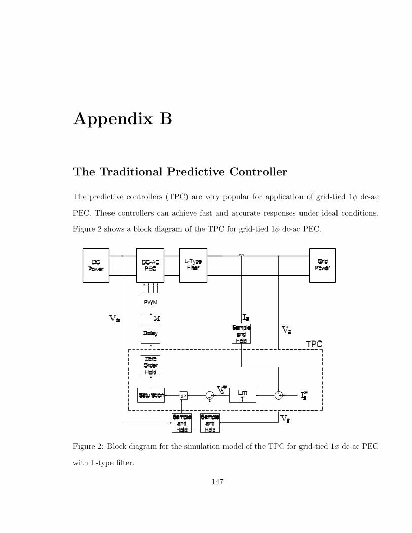
Appendix B
The Traditional Predictive Controller
The predictive controllers (TPC) are very popular for application of grid-tied 1φ dc-ac
PEC. These controllers can achieve fast and accurate responses under ideal conditions.
Figure 2 shows a block diagram of the TPC for grid-tied 1φ dc-ac PEC.
Figure 2: Block diagram for the simulation model of the TPC for grid-tied 1φ dc-ac PEC
with L-type filter.
147

The Predictive Controller with Delay Compensator
The Predictive Controllers with Delay Compensator (PCDC) are an improved version of
the predictive controller. In these controllers, the effect of the control delay is minimized
by using a compensator, as shown by the block diagram in Figure. 3.
Figure 3: Block diagram for the simulation model of the PCDC for grid-tied 1φ dc-ac
PEC with L-type filter.
148

Appendix C
Dead-beat current controllers, disturbance estimators, and observers are implemented
using the TMS320LF240 fixed-point DSP as shown in Figure 4. The TMS320LF240
DSP can implement 40 million instructions per second with 16-bit fixed point processor
and on-chip 10-bit ADC. The software code is designed as modular in C and C-callable
assembly language. The assembly language is used in order to minimize the computation
time and the delay of the controllers.
Figure 4: The digital signal processing board used in this thesis.
149

Code for the Grid-Connected 1φ VS DC-AC PEC with
L-Type Filter
Current Controller Header File Code
1 /∗ ==============================================================================
2 System Name : S i ng l e phase i n v e r t e r cur r ent c on t r o l
3
4 F i l e Name : i n v1 cn t l 2 . h
5
6 Desc r ip t i on : Header f i l e f o r p e r i ph e r a l independent ob j e c t f o r implementation o f
7 cur rent c o n t r o l l e r f o r s i n g l e i n v e r t e r .
8 Or ig inato r : UNB
9
10 Target dependency : x2407
11
12 Note that the PWM i s running at 10 kHz us ing
13 x2407 with 40 MHz c lock .
14
15 =====================================================================================
16 History :
17 −−−−−−−−−−−−−−−−−−−−−−−−−−−−−−−−−−−−−−−−−−−−−−−−−−−−−−−−−−−−−−−−−−−−−−−−−−−−−−−−−−−−−
18 03−13−2008 Release Rev 1 .0 by Shao Riming
19 07−28−2008 Rev 2 .0 by Riming Shao
20 −−−− new d i g i t a l c o n t r o l l e r
21 07−31−2008 Rev 3 .0 by Riming Shao
22 −−−− add d i g i t a l c n t l 2 with i n t e r n a l po l e s
23 08−19−2008 Rev 3 .1 by Riming Shao
24 −−−− reduce iC1 by ha l f
25 11−29−2008 Rev 3 .2 by Riming Shao
26 −−−− bugf ixed in d i g i t a l c n t l 2
27 −−−− remove Rev 3 .1 by r e s t o r i n g iC1 ∗ 2
28 04−24−2009 Rev 3 .3 by Riming Shao
29 −−−− r ea r range iC1 to Q12 (∗ 2) to prevent over f l ow with big L
30 06−02−2016 Rev 4 .0 by Haider Mohomad
31 −−−− new d i g i t a l c o n t r o l l e r
32
150

33
34 ================================================================================= ∗/
35
36 #i f n d e f INV1 CNTL2 H
37 #de f i n e INV1 CNTL2 H
38
39
40 #inc lude <always . h>
41 #inc lude <F2407PWM INV.H>
42 #inc lude <d i g i t a l c n t l 2 . h>
43 #inc lude <d i s t e s t . h>
44
45 /∗−−−−−−−−−−−−−−−−−−−−−−−−−−−−−−−−−−−−−−−−−−−−−−−−−−−−−−−−−−−−−−−−−−−−−−−−−−−−−−
46 Def ine the s t r u c tu r e o f the Object .
47 −−−−−−−−−−−−−−−−−−−−−−−−−−−−−−−−−−−−−−−−−−−−−−−−−−−−−−−−−−−−−−−−−−−−−−−−−−−−−−∗/
48
49 typede f s t r u c t
50
51 /∗−−−−−−−−−−−−−−−−−−−−−−−−−−−−−−−−−−−−−−−−−−−−−−−−−−−−−−−−−−−−−−−−−−−−−−−−−−−−−−
52 Dec l a ra t i on s f o r the ’ t e rmina l v a r i a b l e s ’ f o r the Algorithm . The framework
53 should communicate such quan t i t i e s as f r e q t e s t i n g , e t c to the a lgor i thm by
54 modifying these te rmina l v a r i a b l e s . I t i s not recommended that the framework
55 d i r e c t l y modify the i n t e r n a l v a r i b l e s o f the a lgor i thm .
56 −−−−−−−−−−−−−−−−−−−−−−−−−−−−−−−−−−−−−−−−−−−−−−−−−−−−−−−−−−−−−−−−−−−−−−−−−−−−−−∗/
57 /∗−−−−−−−−−−−−−−−−−−−−−−−−−−−−−−−−−−−−−−−−−−−−−−−−−−−−−−−−−−−−−−−−−−−−−−−−−−−−−
58 Misce l l aneous Items .
59 −−−−−−−−−−−−−−−−−−−−−−−−−−−−−−−−−−−−−−−−−−−−−−−−−−−−−−−−−−−−−−−−−−−−−−−−−−−−−∗/
60 v o l a t i l e in t16 ∗ p i I a ; // Q15
61 v o l a t i l e in t16 ∗ piVgr id ; // Q15
62 v o l a t i l e in t16 ∗ piVdc ; // Q15 ,
63 i n t16 i I r e f ; // Q15
64 i n t16 i I o b s e r v e r ; // Q15
65 i n t16 iC1 ; // Q12 , C1 = L/T∗IMAX/VDCMAX∗2ˆ12
66 i n t16 iC2 ; // Q12 , C2 = VGRIDMAX/VDCMAX∗2ˆ12
67 i n t16 iC3 ; // Q12 , C3 = Gain∗IMAX/VDCMAX∗2ˆ12
68 i n t16 iD ; // Q15 , duty cy c l e r a t i o
69
70 /∗−−−−−−−−−−−−−−−−−−−−−−−−−−−−−−−−−−−−−−−−−−−−−−−−−−−−−−−−−−−−−−−−−−−−−−−−−−−−−−
71 Dec la ra t i on f o r the PWM con t r o l l e r ob j e c t . The d e f a u l t s are s e t in
151

72 F2407PWM INV.H
73 −−−−−−−−−−−−−−−−−−−−−−−−−−−−−−−−−−−−−−−−−−−−−−−−−−−−−−−−−−−−−−−−−−−−−−−−−−−−−−∗/
74 PWMINVGEN pwm;
75
76 /∗−−−−−−−−−−−−−−−−−−−−−−−−−−−−−−−−−−−−−−−−−−−−−−−−−−−−−−−−−−−−−−−−−−−−−−−−−−−−−−
77 Dec la ra t i on f o r the d i g i t a l c o n t r o l l e r ob j e c t . The d e f a u l t s are s e t in
78 d i g i t a l c n t l 2 . h
79 −−−−−−−−−−−−−−−−−−−−−−−−−−−−−−−−−−−−−−−−−−−−−−−−−−−−−−−−−−−−−−−−−−−−−−−−−−−−−−∗/
80 // DIGITAL CNTL2 d i g i t c n t l 2 ;
81 DIST EST d i s t e s t ;
82
83 /∗−−−−−−−−−−−−−−−−−−−−−−−−−−−−−−−−−−−−−−−−−−−−−−−−−−−−−−−−−−−−−−−−−−−−−−−−−−−−−−
84 Dec la ra t i on f o r the f unc t i on s implemented in i nv1 cn t l 2 . c
85 −−−−−−−−−−−−−−−−−−−−−−−−−−−−−−−−−−−−−−−−−−−−−−−−−−−−−−−−−−−−−−−−−−−−−−−−−−−−−−∗/
86 void (∗ i n i t ) ( ) ; // po in t e r to a func t i on
87 void (∗ update ) ( ) ;
88 void (∗ d i s ab l e ) ( ) ;
89 void (∗ enable ) ( ) ;
90
91 INV1 CNTL2 ;
92
93
94 #de f i n e INV1 CNTL2 INITVALS \
95 \
96 ( in t16 ∗) 0 , \
97 ( in t16 ∗) 0 , \
98 ( in t16 ∗) 0 , \
99 0 , \
100 0 , \
101 0 , \
102 0 , \
103 0 , \
104 0 , \
105 PWMINVGENDEFAULTS, \
106 DIST EST INITVALS , \
107 ( void (∗ ) ( ) ) inv1Cnt l2 In i t , \
108 ( void (∗ ) ( ) ) inv1Cntl2Update , \
109 ( void (∗ ) ( ) ) inv1Cnt l2Disable , \
110 ( void (∗ ) ( ) ) inv1Cntl2Enable \
152
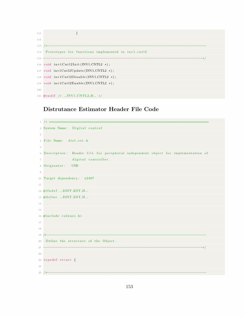
111
112
113 /∗−−−−−−−−−−−−−−−−−−−−−−−−−−−−−−−−−−−−−−−−−−−−−−−−−−−−−−−−−−−−−−−−−−−−−−−−−−−−−−
114 Prototypes f o r f un c t i on s implemented in i nv1 cn t l 2
115 −−−−−−−−−−−−−−−−−−−−−−−−−−−−−−−−−−−−−−−−−−−−−−−−−−−−−−−−−−−−−−−−−−−−−−−−−−−−−−∗/
116 void inv1Cnt l 2 In i t (INV1 CNTL2 ∗) ;
117 void inv1Cntl2Update (INV1 CNTL2 ∗) ;
118 void inv1Cnt l2Disab le (INV1 CNTL2 ∗) ;
119 void inv1Cntl2Enable (INV1 CNTL2 ∗) ;
120
121 #end i f /∗ INV1 CNTL2 H ∗/
Distrutance Estimator Header File Code
1 /∗ ==============================================================================
2 System Name : D i g i t a l c on t r o l
3
4 F i l e Name : d i s t e s t . h
5
6 Desc r ip t i on : Header f i l e f o r p e r i ph e r a l independent ob j e c t f o r implementation o f
7 d i g i t a l c o n t r o l l e r .
8 Or ig inato r : UNB
9
10 Target dependency : x2407
11
12 #i f n d e f DIST EST H
13 #de f i n e DIST EST H
14
15
16 #inc lude <always . h>
17
18
19 /∗−−−−−−−−−−−−−−−−−−−−−−−−−−−−−−−−−−−−−−−−−−−−−−−−−−−−−−−−−−−−−−−−−−−−−−−−−−−−−−
20 Def ine the s t r u c tu r e o f the Object .
21 −−−−−−−−−−−−−−−−−−−−−−−−−−−−−−−−−−−−−−−−−−−−−−−−−−−−−−−−−−−−−−−−−−−−−−−−−−−−−−∗/
22
23 typede f s t r u c t
24
25 /∗−−−−−−−−−−−−−−−−−−−−−−−−−−−−−−−−−−−−−−−−−−−−−−−−−−−−−−−−−−−−−−−−−−−−−−−−−−−−−−
153
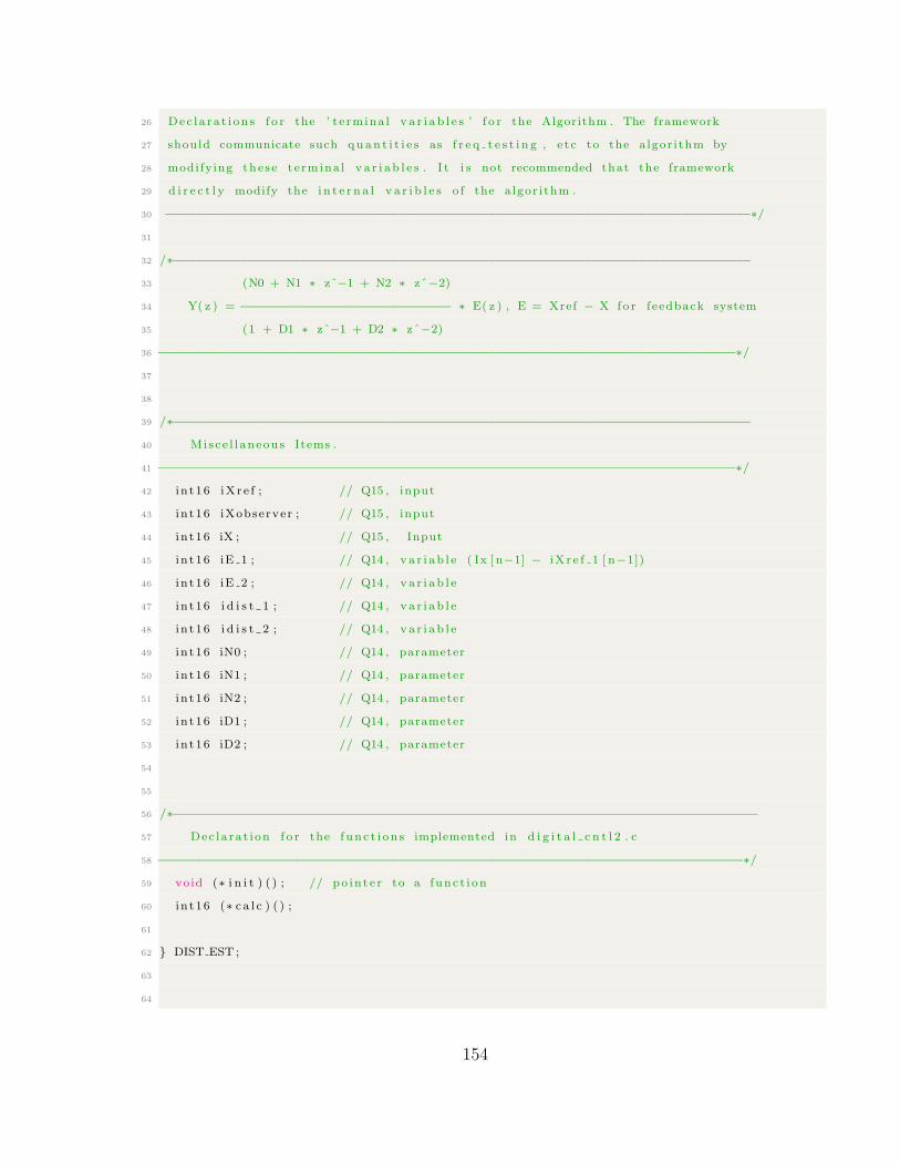
26 Dec l a ra t i on s f o r the ’ t e rmina l v a r i a b l e s ’ f o r the Algorithm . The framework
27 should communicate such quan t i t i e s as f r e q t e s t i n g , e t c to the a lgor i thm by
28 modifying these te rmina l v a r i a b l e s . I t i s not recommended that the framework
29 d i r e c t l y modify the i n t e r n a l v a r i b l e s o f the a lgor i thm .
30 −−−−−−−−−−−−−−−−−−−−−−−−−−−−−−−−−−−−−−−−−−−−−−−−−−−−−−−−−−−−−−−−−−−−−−−−−−−−−−∗/
31
32 /∗−−−−−−−−−−−−−−−−−−−−−−−−−−−−−−−−−−−−−−−−−−−−−−−−−−−−−−−−−−−−−−−−−−−−−−−−−−−−−
33 (N0 + N1 ∗ zˆ−1 + N2 ∗ zˆ−2)
34 Y( z ) = −−−−−−−−−−−−−−−−−−−−−−−−−−−− ∗ E( z ) , E = Xref − X fo r feedback system
35 (1 + D1 ∗ zˆ−1 + D2 ∗ zˆ−2)
36 −−−−−−−−−−−−−−−−−−−−−−−−−−−−−−−−−−−−−−−−−−−−−−−−−−−−−−−−−−−−−−−−−−−−−−−−−−−−−∗/
37
38
39 /∗−−−−−−−−−−−−−−−−−−−−−−−−−−−−−−−−−−−−−−−−−−−−−−−−−−−−−−−−−−−−−−−−−−−−−−−−−−−−−
40 Misce l l aneous Items .
41 −−−−−−−−−−−−−−−−−−−−−−−−−−−−−−−−−−−−−−−−−−−−−−−−−−−−−−−−−−−−−−−−−−−−−−−−−−−−−∗/
42 i n t16 iXr e f ; // Q15 , input
43 i n t16 iXobserver ; // Q15 , input
44 i n t16 iX ; // Q15 , Input
45 i n t16 iE 1 ; // Q14 , v a r i ab l e ( Ix [ n−1] − iX r e f 1 [ n−1])
46 i n t16 iE 2 ; // Q14 , v a r i ab l e
47 i n t16 i d i s t 1 ; // Q14 , v a r i ab l e
48 i n t16 i d i s t 2 ; // Q14 , v a r i ab l e
49 i n t16 iN0 ; // Q14 , parameter
50 i n t16 iN1 ; // Q14 , parameter
51 i n t16 iN2 ; // Q14 , parameter
52 i n t16 iD1 ; // Q14 , parameter
53 i n t16 iD2 ; // Q14 , parameter
54
55
56 /∗−−−−−−−−−−−−−−−−−−−−−−−−−−−−−−−−−−−−−−−−−−−−−−−−−−−−−−−−−−−−−−−−−−−−−−−−−−−−−−
57 Dec la ra t i on f o r the f unc t i on s implemented in d i g i t a l c n t l 2 . c
58 −−−−−−−−−−−−−−−−−−−−−−−−−−−−−−−−−−−−−−−−−−−−−−−−−−−−−−−−−−−−−−−−−−−−−−−−−−−−−−∗/
59 void (∗ i n i t ) ( ) ; // po in t e r to a func t i on
60 i n t16 (∗ c a l c ) ( ) ;
61
62 DIST EST ;
63
64
154

65 #de f i n e DIST EST INITVALS \
66 \
67 0 , \
68 0 , \
69 0 , \
70 0 , \
71 0 , \
72 0 , \
73 0 , \
74 0 , \
75 0 , \
76 0 , \
77 0 , \
78 0 , \
79 ( void (∗ ) ( ) ) d i s tE s t I n i t , \
80 ( in t16 (∗ ) ( ) ) d i s tEs tCa l c \
81
82
83 /∗−−−−−−−−−−−−−−−−−−−−−−−−−−−−−−−−−−−−−−−−−−−−−−−−−−−−−−−−−−−−−−−−−−−−−−−−−−−−−−
84 Prototypes f o r f un c t i on s implemented in d i g i t a l c n t l 2 . c or d i g i t a l c n t l 2 a . asm
85 −−−−−−−−−−−−−−−−−−−−−−−−−−−−−−−−−−−−−−−−−−−−−−−−−−−−−−−−−−−−−−−−−−−−−−−−−−−−−−∗/
86 void d i s t E s t I n i t (DIST EST ∗) ;
87 i n t16 d i s tEs tCa l c (DIST EST ∗) ;
88
89 #end i f /∗ DIST EST H ∗/
Current Controller Assembly Code
1 ; /∗ ==============================================================================
2 ; System Name : S i ng l e phase i n v e r t e r
3
4 ; F i l e Name : i n v 1 cn t l 2 a . asm
5
6 ; De s c r ip t i on : implementation o f cur r ent c on t r o l f o r s i n g l e phase i n v e r t e r .
7 ; Or i g ina to r : UNB
8
9 ; Target dependency : x2407
10 ;=====================================================================================
11 ; H i s tory :
155

12 ;−−−−−−−−−−−−−−−−−−−−−−−−−−−−−−−−−−−−−−−−−−−−−−−−−−−−−−−−−−−−−−−−−−−−−−−−−−−−−−−−−−−−−
13 ; 03−14−2008 Release Rev 1 .0 by Shao Riming
14 ; 07−28−2008 Rev 2 .0 by Riming Shao
15 ; −−−− new d i g i t a l c o n t r o l l e r
16 ; 07−31−2008 Rev 3 .0 by Riming Shao
17 ; −−−− add d i g i t a l c n t l 2 with i n t e r n a l po l e s
18 ; 08−19−2008 Rev 3 .1 by Riming Shao
19 ; −−−− reduce iC1 by ha l f
20 ; 11−29−2008 Rev 3 .2 by Riming Shao
21 ; −−−− bugf ixed in d i g i t a l c n t l 2
22 ; −−−− remove Rev 3 .1 by r e s t o r i n g iC1 ∗ 2
23 ; 04−24−2009 Rev 3 .3 by Riming Shao
24 ; −−−− r ea r range iC1 to Q12 (∗ 2) to prevent over f l ow with big L
25 ; 06−02−2016 Rev 4 .0 by Haider Mohomad
26 ; −−−− new d i g i t a l c o n t r o l l e r
27 ;================================================================================= ∗/
28
29 ;================================================================================
30 ; Routine Name : INV1 CNTL2 Routine Type : C Ca l l ab l e
31 ;
32 ; De s c r ip t i on :
33 ;
34 ; C prototype : void inv1Cntl2Update (INV1 CNTL2 ∗p) ;
35 ; H i s tory c rea ted July 31 , 2008
36 ;================================================================================
37 ; D e f i n i t i o n o f INV1 CNTL2
38 ; /∗−−−−−−−−−−−−−−−−−−−−−−−−−−−−−−−−−−−−−−−−−−−−−−−−−−−−−−−−−−−−−−−−−−−−−−−−−−−−−−
39 ; Def ine the s t r u c tu r e o f the Object .
40 ;−−−−−−−−−−−−−−−−−−−−−−−−−−−−−−−−−−−−−−−−−−−−−−−−−−−−−−−−−−−−−−−−−−−−−−−−−−−−−−∗/
41 ;
42 ; typede f s t r u c t
43 ;
44 ; /∗−−−−−−−−−−−−−−−−−−−−−−−−−−−−−−−−−−−−−−−−−−−−−−−−−−−−−−−−−−−−−−−−−−−−−−−−−−−−−−
45 ; Dec l a ra t i on s f o r the ’ t e rmina l v a r i a b l e s ’ f o r the Algorithm . The framework
46 ; should communicate such quan t i t i e s as f r e q t e s t i n g , e t c to the a lgor i thm by
47 ; modifying these te rmina l v a r i a b l e s . I t i s not recommended that the framework
48 ; d i r e c t l y modify the i n t e r n a l v a r i b l e s o f the a lgor i thm .
49 ; −−−−−−−−−−−−−−−−−−−−−−−−−−−−−−−−−−−−−−−−−−−−−−−−−−−−−−−−−−−−−−−−−−−−−−−−−−−−−−∗/
50 ; /∗−−−−−−−−−−−−−−−−−−−−−−−−−−−−−−−−−−−−−−−−−−−−−−−−−−−−−−−−−−−−−−−−−−−−−−−−−−−−−
156

51 ; Mi s ce l l aneous Items .
52 ;−−−−−−−−−−−−−−−−−−−−−−−−−−−−−−−−−−−−−−−−−−−−−−−−−−−−−−−−−−−−−−−−−−−−−−−−−−−−−∗/
53 ; v o l a t i l e in t16 ∗ p i I a ; // Q15
54 ; v o l a t i l e in t16 ∗ piVgr id ; // Q15
55 ; v o l a t i l e in t16 ∗ piVdc ; // Q15 ,
56 ; i n t16 i I r e f ; // Q15
57 ; i n t16 i IObserve ; // Q15
58 ; i n t16 iC1 ; // Q12 , C1 = L/T∗IMAX/VDCMAX∗2ˆ12
59 ; i n t16 iC2 ; // Q12 , C2 = VGRIDMAX/VDCMAX∗2ˆ12
60 ; i n t16 iC3 ; // Q13 , C3 = Gain∗IMAX/VDCMAX∗2ˆ13
61 ; i n t16 iD ; // Q15 , duty cy c l e r a t i o
62 ;
63 ; /∗−−−−−−−−−−−−−−−−−−−−−−−−−−−−−−−−−−−−−−−−−−−−−−−−−−−−−−−−−−−−−−−−−−−−−−−−−−−−−−
64 ; Dec la ra t i on f o r the PWM con t r o l l e r ob j e c t . The d e f a u l t s are s e t in
65 ; F2407PWM INV.H
66 ;−−−−−−−−−−−−−−−−−−−−−−−−−−−−−−−−−−−−−−−−−−−−−−−−−−−−−−−−−−−−−−−−−−−−−−−−−−−−−−∗/
67 ; PWMINVGEN pwm;
68 ;
69 ; /∗−−−−−−−−−−−−−−−−−−−−−−−−−−−−−−−−−−−−−−−−−−−−−−−−−−−−−−−−−−−−−−−−−−−−−−−−−−−−−−
70 ; Dec la ra t i on f o r the d i g i t a l c o n t r o l l e r ob j e c t . The d e f a u l t s are s e t in
71 ; d i g i t a l c n t l 2 . h
72 ;−−−−−−−−−−−−−−−−−−−−−−−−−−−−−−−−−−−−−−−−−−−−−−−−−−−−−−−−−−−−−−−−−−−−−−−−−−−−−−∗/
73 ; DIST EST d i s t e s t ;
74 ;
75 ;
76 ; /∗−−−−−−−−−−−−−−−−−−−−−−−−−−−−−−−−−−−−−−−−−−−−−−−−−−−−−−−−−−−−−−−−−−−−−−−−−−−−−−
77 ; Dec la ra t i on f o r the f unc t i on s implemented in i nv1 cn t l 2 . c
78 ;−−−−−−−−−−−−−−−−−−−−−−−−−−−−−−−−−−−−−−−−−−−−−−−−−−−−−−−−−−−−−−−−−−−−−−−−−−−−−−∗/
79 ; void (∗ i n i t ) ( ) ; // po in t e r to a func t i on
80 ; void (∗ update ) ( ) ;
81 ; void (∗ d i s ab l e ) ( ) ;
82 ; void (∗ enable ) ( ) ;
83 ;
84 ; INV1 CNTL2 ;
85
86
87 ;−−−−−−−−−−−−−−−−−−−−−−−−−−−−−−−−−−−−−−−−−−
88 ;COMPENSATION RATIO FOR DEADBAND OF DRIVER
89 ;−−−−−−−−−−−−−−−−−−−−−−−−−−−−−−−−−−−−−−−−−−
157

90 DBCOMPENSATION . s e t 3145 ; 2293 ; 2 2 9 3 ; X% ∗ 32767
91
92
93 . i n c lude . . \ i n c lude \x240x . h
94
95 . de f inv1Cntl2Update
96
97 inv1Cntl2Update :
98
99 i nv1Cnt l2Update f rames i z e . s e t 2
100
101 ;−−−−−−−−−−−−−−−−−−−−−−−−−−−−−−−−−−−−−−−−−−−−−−−−−−−−−−−−−−−−−−−−−−−−−−−−−−
102 ; ARP = AR1
103 ; AR1 i s s tack po in t e r (SP)
104 ; AR0 i s frame po in t e r (FP)
105 POPD ∗+ ; Save the re turn address from hardware
106 ; s tack onto the so f tware s tack
107 ; ARP = AR1
108
109 SAR AR0, ∗+ ; push AR0(FP) . ARP =AR1
110 SAR AR1, ∗ ; ∗SP = SP . ARP =AR1
111 LAR AR0, # inv1Cnt l2Update f rames i z e
112 ; FP = s i z e o f frame
113 LAR AR0, ∗0+, AR2 ; ARP = AR2.
114 ; A l l o ca t e frame . AR0 = ∗AR1
115 ; AR1 = AR1 + AR0.
116 ;−−−−−−−−−−−−−−−−−−−−−−−−−−−−−−−−−−−−−−−−−−−−−−−−−−−−−−−−−−−−−−−−−−−−−−−−−−
117 LAR AR2, #−3
118 MAR ∗0+ ; AR2 pts to f i r s t arguments , −− to next one
119 ; ARP = AR2, AR2 −> p
120 ;−−−−−−−−−−−−−−−−−−−−−−−−−−−−−−−−−−−−−−−−−−−−−−−−−−−−−−−−−−−−−−−−−−−−−−−−−−
121 LAR AR3,∗ ; AR3 po in t s to the f i r s t s t r u c tu r e member
122 ; ( i . e . AR3 −> p i I a ) . ARP = AR2
123 ; AR3 −> p i I a .
124 ;−−−−−−−−−−−−−−−−−−−−−−−−−−−−−−−−−−−−−−−−−−−−−−−−−−−−−−−−−−−−−−−−−−−−−−−−−−
125 LAR AR2,∗ ; AR2 po in t s to the f i r s t s t r u c tu r e member
126 ; ( i . e . AR2 −> p i I a ) . ARP = AR2.
127 ; AR2 −> p i I a .
128 ;−−−−−−−−−−−−−−−−−−−−−−−−−−−−−−−−−−−−−−−−−−−−−−−−−−−−−−−−−−−−−−−−−−−−−−−−−−
158
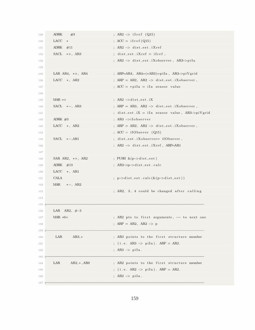
129 ADRK #3 ; AR2 −> i I r e f (Q15)
130 LACC ∗ ; ACC = i I r e f (Q15)
131 ADRK #11 ; AR2 −> d i s t e s t . iX r e f
132 SACL ∗+, AR3 ; d i s t e s t . iX r e f = i I r e f ,
133 ; AR2 −> d i s t e s t . iXobserver , AR3−>p i I a
134
135 LAR AR4, ∗+, AR4 ; ARP=AR4, AR4=(∗AR3)=piIa , AR3−>piVgr id
136 LACC ∗ , AR2 ; ARP = AR2, AR2 −> d i s t e s t . iXobserver ,
137 ; ACC = ∗ p i I a = i I a s enso r va lue
138
139 MAR ∗+ ; AR2 −>d i s t e s t . iX
140 SACL ∗−, AR3 ; ARP = AR3, AR2 −> d i s t e s t . iXobserver ,
141 ; d i s t e s t . iX = i I a s enso r value , AR3−>piVgr id
142 ADRK #3 ; AR3 −> i I o b s e r v e r
143 LACC ∗ , AR2 ; ARP = AR2, AR2 −> d i s t e s t . iXobserver ,
144 ; ACC = iIObsever (Q15)
145 SACL ∗−,AR1 ; d i s t e s t . iXobserver= iIObsever ,
146 ; AR2 −> d i s t e s t . iXre f , ARP=AR1
147
148 SAR AR2, ∗+, AR2 ; PUSH &(p−>d i s t e s t )
149 ADRK #13 ; AR2−>p−>d i s t e s t . c a l c
150 LACC ∗ , AR1
151 CALA ; p−>d i s t e s t . c a l c (&(p−>d i s t e s t ) )
152 MAR ∗−, AR2
153 ; AR2, 3 , 4 could be changed a f t e r c a l l i n g
154
155 ;−−−−−−−−−−−−−−−−−−−−−−−−−−−−−−−−−−−−−−−−−−−−−−−−−−−−−−−−−−−−−−−−−−−−−−−−−−
156 LAR AR2, #−3
157 MAR ∗0+ ; AR2 pts to f i r s t arguments , −− to next one
158 ; ARP = AR2, AR2 −> p
159 ;−−−−−−−−−−−−−−−−−−−−−−−−−−−−−−−−−−−−−−−−−−−−−−−−−−−−−−−−−−−−−−−−−−−−−−−−−−
160 LAR AR3,∗ ; AR3 po in t s to the f i r s t s t r u c tu r e member
161 ; ( i . e . AR3 −> p i I a ) . ARP = AR2.
162 ; AR3 −> p i I a .
163 ;−−−−−−−−−−−−−−−−−−−−−−−−−−−−−−−−−−−−−−−−−−−−−−−−−−−−−−−−−−−−−−−−−−−−−−−−−−
164 LAR AR2,∗ ,AR0 ; AR2 po in t s to the f i r s t s t r u c tu r e member
165 ; ( i . e . AR2 −> p i I a ) . ARP = AR2.
166 ; AR2 −> p i I a .
167 ;−−−−−−−−−−−−−−−−−−−−−−−−−−−−−−−−−−−−−−−−−−−−−−−−−−−−−−−−−−−−−−−−−−−−−−−−−−
159

168 SETC SXM
169 SETC OVM
170
171 SACL ∗+, AR2 ; Store the est imated d i s turbance in the f i r s t frame l o c a t i o n
i d i s t , ARP=AR2; then move AR0 to po int f o r the second frame l o c a t i o n f o r the
c a l c u l a t i o n o f i e=I r e f−I obse rve ( d i f f e r e n t from IE which i s Ix−I obse rve )
172
173
174 ADRK #3 ; ARP=AR2, AR2−> i I r e f Q(15)
175 LACC ∗+ ; ACC = i I r e f , ARP=AR2−> i I o b s e r v e r (Q15)
176 SUB ∗+, AR0 ; ARP = AR0, ACC=i I r e f −i I o b s e r v e r (Q15) , AR2−>iC1 , AR0−>i e
177 ; SFR ; To change ACC from Q15 to Q14
178 SACL ∗ ; ARP = AR0, i e=i I r e f −i I ob s e r v e r , AR2−>iC1 , AR3−>
179
180 LT ∗−, AR2 ; T = i e (Q15) , ARP=AR2−>iC1 (Q12) , AR0−> i d i s t
181
182 MPY ∗+ ; AR2−>iC2 , P=i e ∗ iC1 (Q27)
183 PAC ; ACC = dI∗C1 without s h i f t (Q27)
184 ; SFL ; ACC = dI∗C1 (Q27)
185 LT ∗+, AR3 ; T=iC2 (Q12) , AR2−>iC3 , ARP=AR3−>p i I a
186 MAR ∗+ ; AR3−>piVgr id
187 LAR AR4, ∗+, AR4 ; ARP=AR4, AR4=piVgrid (Q15) , AR3−>piVdc
188 MPY ∗ , AR2 ; ARP=AR2−>iC3 (Q13) P = iC2∗Vgrid (Q27) We mult ip ly to iC2
to conve r t e r Vgrid from (Q15) to (Q27)
189 ; APAC ; ACC = dI∗C1 + Vgrid∗C2 (Q27) JUne 6 comment t h i s s i n c e i
w i l l use MPYA
190 LT ∗+,AR0 ; T = iC3 , ARP=AR0−> i d i s t (Q14) , AR2−>iD
191 MPYA ∗ ; P = i d i s t ∗ iC3 (Q27) , ACC = dI∗C1 + Vgrid∗C2 (Q27)
192 ;MAR ∗ , AR0 ; ARP = AR0−> i d i s t (Q14)
193 ;SUB ∗ , 13 ; ACC = dI∗C1 + Vgrid∗C2 − i d i s t (Q27) , the 13 b i t s s h i f t o f
i d i s t to make i t Q27 as we l l
194 SPAC ; ACC = dI∗C1 + Vgrid∗C2 − i d i s t ∗C3 (Q27)
195
196 SPLK #1, ∗
197 BCND POS VALUE, GEQ
198 SPLK #−1, ∗
199 ABS
200 POS VALUE:
201 LT ∗ , AR3 ; AR3−>piVdc
160

202 LAR AR4, ∗ , AR4 ; ARP=AR4, AR4=piVdc , AR3−>piVdc
203 SUB ∗ , 12 ; Q27
204 BCND POS NOT OV, LT
205 LACC #32767
206 MAR ∗ , AR0
207 B SIGN ADJ
208
209 POS NOT OV:
210 ADD ∗ , 12 ; ACC=dI∗C1 + Vgrid∗C2 − i d i s t (Q27)
211 RPT #2
212 SFL
213 RPT #15
214 SUBC ∗ ; ACC = Reminder | r e s u l t s
215 MAR ∗ , AR0 ; ACC=(dI∗C1 + Vgrid∗C2) /Vdc (Q15) , ARP = AR0
216 SIGN ADJ :
217 SACL ∗ ; Frame (1) = ( dI∗C1 + Vgrid∗C2) /Vdc (Q15) = duty
218 MPY ∗ , AR2 ; AR2−>iD ; T has the s ign , P=T∗duty
219 PAC ; ACC = duty with s i gn adjusted
220 SACL ∗ ; iD=duty
221 BCND ZEROCOMP, EQ
222 BCND NEGCOMP, LT
223 ADD #DBCOMPENSATION
224 SACL ∗
225 SUB #32767
226 BCND ZEROCOMP, LEQ
227 SPLK #32767 , ∗
228 B ZEROCOMP
229 NEGCOMP:
230 SUB #DBCOMPENSATION
231 SACL ∗
232 SUB #−32767
233 BCND ZEROCOMP, GEQ
234 SPLK #−32767, ∗
235 B ZEROCOMP
236
237 ZEROCOMP:
238 LACC ∗+ ; ACC=RESULT, AR2−>pwm
239
240 CLRC OVM
161

241
242 ADRK #2 ; AR2−>p−>pwm. duty c1
243 SACL ∗ ; p−>pwm. duty c1=RESULT
244 SBRK #2 ; AR2−>pwm
245 MAR ∗ , AR1
246 SAR AR2, ∗+, AR2 ; PUSH &(p−>pwm)
247 ADRK #4 ; AR2−>p−>pwm. update
248 LACC ∗ , AR1
249 CALA ; p−>pwm. update (&(p−>pwm) )
250
251 ; Update the obse rve r
252 MAR ∗−,AR2 ; ARP=AR2−>duty c1 ;
253 SBRK #8 ; AR2−> i I r e f
254 LACC ∗+ ; ACC=i I r e f , AR2−>i I o b s e r v e r
255 SACL ∗ ,AR1 ; i I o b s e r v e r = i I r e f
256
257
258
259
260 i nv1Cnt l2Update ex i t :
261
262 ; MAR ∗ ,AR1 ; can be removed i f t h i s cond i t i on i s met on
263 ; every path to t h i s code .
264 ; s e t ARP = SP be f o r e you e x i t .
265 SBRK #( inv1Cnt l2Update f rames i z e+1)
266 ; d e a l l o c a t e frame , po int to saved FP
267 LAR AR0, ∗− ; r e s t o r e frame po in t e r
268 PSHD ∗ ; push re turn address on hardware s tack
269
270 RET
271
272 . end
Disturbance Estimator Assembly Code
1 ; /∗ ==============================================================================
2 ; System Name : S i ng l e phase i n v e r t e r
3
4 ; F i l e Name : d i s t e s t a . asm
162

5
6 ; De s c r ip t i on : implementation o f d i s tu rbance e s t imator .
7 ; Or i g ina to r : UNB
8
9 ; Target dependency : x2407
10 ;=====================================================================================
11 ; H i s tory :
12 ;−−−−−−−−−−−−−−−−−−−−−−−−−−−−−−−−−−−−−−−−−−−−−−−−−−−−−−−−−−−−−−−−−−−−−−−−−−−−−−−−−−−−−
13 ; 07−31−2008 Rev 1 .0 by Riming Shao
14 ;
15 ; 11−29−2008 Rev 2 .0 by Riming Shao
16 ; bug f ix : iE and iY need to be Q14
17 ;
18 ; 05−27−2016 Created by Haider Mohomad from d i g i t a l c o n t r o l l e r
================================================================================= ∗/
19
20 ;================================================================================
21 ; Routine Name : DIST EST Routine Type : C Ca l l ab l e
22 ;
23 ; De s c r ip t i on :
24 ;
25 ; C prototype : void d i s t E s t I n i t (DIGITAL CNTL1 ∗) ;
26 ; i n t16 d i s tEs tCa l c (DIGITAL CNTL1 ∗) ;
27 ; H i s tory c rea ted May 27 , 2016
28 ;================================================================================
29 ; D e f i n i t i o n o f DIST EST
30 ; /∗−−−−−−−−−−−−−−−−−−−−−−−−−−−−−−−−−−−−−−−−−−−−−−−−−−−−−−−−−−−−−−−−−−−−−−−−−−−−−−
31 ; Def ine the s t r u c tu r e o f the Object .
32 ;−−−−−−−−−−−−−−−−−−−−−−−−−−−−−−−−−−−−−−−−−−−−−−−−−−−−−−−−−−−−−−−−−−−−−−−−−−−−−−∗/
33 ;
34 ; /∗−−−−−−−−−−−−−−−−−−−−−−−−−−−−−−−−−−−−−−−−−−−−−−−−−−−−−−−−−−−−−−−−−−−−−−−−−−−−−−
35 ; Def ine the s t r u c tu r e o f the Object .
36 ;−−−−−−−−−−−−−−−−−−−−−−−−−−−−−−−−−−−−−−−−−−−−−−−−−−−−−−−−−−−−−−−−−−−−−−−−−−−−−−∗/
37 ;
38 ; typede f s t r u c t
39 ;
40 ; /∗−−−−−−−−−−−−−−−−−−−−−−−−−−−−−−−−−−−−−−−−−−−−−−−−−−−−−−−−−−−−−−−−−−−−−−−−−−−−−−
41 ; Dec l a ra t i on s f o r the ’ t e rmina l v a r i a b l e s ’ f o r the Algorithm . The framework
42 ; should communicate such quan t i t i e s as f r e q t e s t i n g , e t c to the a lgor i thm by
163

43 ; modifying these te rmina l v a r i a b l e s . I t i s not recommended that the framework
44 ; d i r e c t l y modify the i n t e r n a l v a r i b l e s o f the a lgor i thm .
45 ; −−−−−−−−−−−−−−−−−−−−−−−−−−−−−−−−−−−−−−−−−−−−−−−−−−−−−−−−−−−−−−−−−−−−−−−−−−−−−−∗/
46 ;
47 ; /∗−−−−−−−−−−−−−−−−−−−−−−−−−−−−−−−−−−−−−−−−−−−−−−−−−−−−−−−−−−−−−−−−−−−−−−−−−−−−−
48 ; (N0 + N1 ∗ zˆ−1 + N2 ∗ zˆ−2)
49 ; d i s t ( z ) = −−−−−−−−−−−−−−−−−−−−−−−−−−−− ∗ E( z ) ,E = X − Xref 1 f o r feedback system
50 ; (1 + D1 ∗ zˆ−1 + D2 ∗ zˆ−2)
51 ;−−−−−−−−−−−−−−−−−−−−−−−−−−−−−−−−−−−−−−−−−−−−−−−−−−−−−−−−−−−−−−−−−−−−−−−−−−−−−∗/
52 ;
53 ;
54 ; /∗−−−−−−−−−−−−−−−−−−−−−−−−−−−−−−−−−−−−−−−−−−−−−−−−−−−−−−−−−−−−−−−−−−−−−−−−−−−−−
55 ; Mi s ce l l aneous Items .
56 ;−−−−−−−−−−−−−−−−−−−−−−−−−−−−−−−−−−−−−−−−−−−−−−−−−−−−−−−−−−−−−−−−−−−−−−−−−−−−−∗/
57 ; i n t16 iXr e f ; // Q15 , input
58 ; i n t16 iXobserve ; // Q15 , input
59 ; i n t16 iX ; // Q15 , Input
60 ; i n t16 iE 1 ; // Q14 , v a r i ab l e ( Ix [ n−1] − iX r e f 1 [ n−1])
61 ; i n t16 iE 2 ; // Q14 , v a r i ab l e
62 ; i n t16 i d i s t 1 ; // Q14 , v a r i ab l e
63 ; i n t16 i d i s t 2 ; // Q14 , v a r i ab l e
64 ; i n t16 iN0 ; // Q14 , parameter
65 ; i n t16 iN1 ; // Q14 , parameter
66 ; i n t16 iN2 ; // Q14 , parameter
67 ; i n t16 iD1 ; // Q14 , parameter
68 ; i n t16 iD2 ; // Q14 , parameter
69 ;
70 ;
71 ; /∗−−−−−−−−−−−−−−−−−−−−−−−−−−−−−−−−−−−−−−−−−−−−−−−−−−−−−−−−−−−−−−−−−−−−−−−−−−−−−−
72 ; Dec la ra t i on f o r the f unc t i on s implemented in d i g i t a l c n t l 2 . c
73 ;−−−−−−−−−−−−−−−−−−−−−−−−−−−−−−−−−−−−−−−−−−−−−−−−−−−−−−−−−−−−−−−−−−−−−−−−−−−−−−∗/
74 ; void (∗ i n i t ) ( ) ; // po in t e r to a func t i on
75 ; i n t16 (∗ c a l c ) ( ) ;
76 ;
77 ; DIST EST ;
78
79
80
81 . i n c lude . . \ i n c lude \x240x . h
164

82
83
84 . de f d i s t E s t I n i t
85
86 d i s t E s t I n i t :
87
88 d i s t E s t I n i t f r am e s i z e . s e t 0
89
90
91 ;−−−−−−−−−−−−−−−−−−−−−−−−−−−−−−−−−−−−−−−−−−−−−−−−−−−−−−−−−−−−−−−−−−−−−−−−−−
92 ; ARP = AR1
93 ; AR1 i s s tack po in t e r (SP)
94 ; AR0 i s frame po in t e r (FP)
95 POPD ∗+ ; Save the re turn address from hardware
96 ; s tack onto the so f tware s tack
97 ; ARP = AR1
98
99 SAR AR0, ∗+ ; push AR0(FP) . ARP =AR1
100 SAR AR1, ∗ ; ∗SP = SP . ARP =AR1
101 LAR AR0, # d i s t E s t I n i t f r am e s i z e
102 ; FP = s i z e o f frame
103 LAR AR0, ∗0+, AR2 ; ARP = AR2.
104 ; A l l o ca t e frame . AR0 = ∗AR1
105 ; AR1 = AR1 + AR0.
106 ;−−−−−−−−−−−−−−−−−−−−−−−−−−−−−−−−−−−−−−−−−−−−−−−−−−−−−−−−−−−−−−−−−−−−−−−−−−
107 LAR AR2, #−3
108 MAR ∗0+ ; AR2 pts to f i r s t arguments , −− to next one
109 ; ARP = AR2, AR2 −> p
110 ;−−−−−−−−−−−−−−−−−−−−−−−−−−−−−−−−−−−−−−−−−−−−−−−−−−−−−−−−−−−−−−−−−−−−−−−−−−
111 LAR AR2,∗ ; AR2 po in t s to the f i r s t s t r u c tu r e member
112 ; ( i . e . AR2 −> iX r e f ) . ARP = AR2.
113 ; AR2 −> iX r e f .
114 ;−−−−−−−−−−−−−−−−−−−−−−−−−−−−−−−−−−−−−−−−−−−−−−−−−−−−−−−−−−−−−−−−−−−−−−−−−−
115 ADRK #3 ; ARP = AR2, AR2−>iE 1
116 LACL #0 ; Load ACC Low with constant 0 , i . e . ACCL=0x00
117 SACL ∗+ ; ARP = AR2, AR2−>iE 2 , iE 1 = ACCL
118 SACL ∗+ ; ARP = AR2, AR2−>i d i s t 1 , iE 2 = ACCL
119 SACL ∗+ ; ARP = AR2, AR2−>i d i s t 2 , i d i s t 1 = ACCL
120 SACL ∗+, AR1 ; ARP = AR1, AR2−>iN 0 , i d i s t 2 = ACCL
165
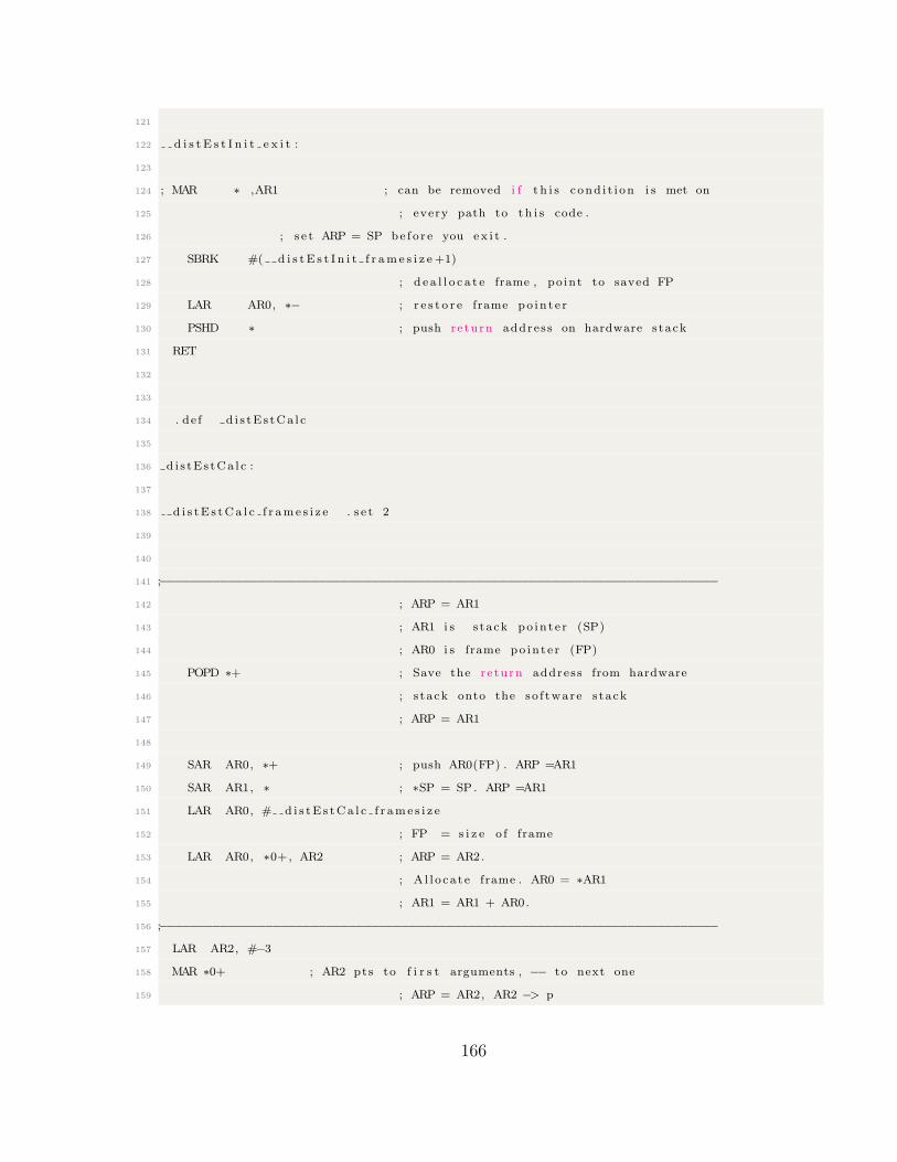
121
122 d i s t E s t I n i t e x i t :
123
124 ; MAR ∗ ,AR1 ; can be removed i f t h i s cond i t i on i s met on
125 ; every path to t h i s code .
126 ; s e t ARP = SP be f o r e you e x i t .
127 SBRK #( d i s t E s t I n i t f r am e s i z e +1)
128 ; d e a l l o c a t e frame , po int to saved FP
129 LAR AR0, ∗− ; r e s t o r e frame po in t e r
130 PSHD ∗ ; push re turn address on hardware s tack
131 RET
132
133
134 . de f d i s tE s tCa l c
135
136 d i s tEs tCa l c :
137
138 d i s tE s tCa l c f r ame s i z e . s e t 2
139
140
141 ;−−−−−−−−−−−−−−−−−−−−−−−−−−−−−−−−−−−−−−−−−−−−−−−−−−−−−−−−−−−−−−−−−−−−−−−−−−
142 ; ARP = AR1
143 ; AR1 i s s tack po in t e r (SP)
144 ; AR0 i s frame po in t e r (FP)
145 POPD ∗+ ; Save the re turn address from hardware
146 ; s tack onto the so f tware s tack
147 ; ARP = AR1
148
149 SAR AR0, ∗+ ; push AR0(FP) . ARP =AR1
150 SAR AR1, ∗ ; ∗SP = SP . ARP =AR1
151 LAR AR0, # d i s tE s tCa l c f r ame s i z e
152 ; FP = s i z e o f frame
153 LAR AR0, ∗0+, AR2 ; ARP = AR2.
154 ; A l l o ca t e frame . AR0 = ∗AR1
155 ; AR1 = AR1 + AR0.
156 ;−−−−−−−−−−−−−−−−−−−−−−−−−−−−−−−−−−−−−−−−−−−−−−−−−−−−−−−−−−−−−−−−−−−−−−−−−−
157 LAR AR2, #−3
158 MAR ∗0+ ; AR2 pts to f i r s t arguments , −− to next one
159 ; ARP = AR2, AR2 −> p
166

160 ;−−−−−−−−−−−−−−−−−−−−−−−−−−−−−−−−−−−−−−−−−−−−−−−−−−−−−−−−−−−−−−−−−−−−−−−−−−
161 LAR AR3,∗ ; AR3 po in t s to the f i r s t s t r u c tu r e member
162 ; ( i . e . AR3 −> iX r e f ) . ARP = AR2.
163 ;−−−−−−−−−−−−−−−−−−−−−−−−−−−−−−−−−−−−−−−−−−−−−−−−−−−−−−−−−−−−−−−−−−−−−−−−−−
164 LAR AR2,∗ ; AR2 po in t s to the f i r s t s t r u c tu r e member
165 ; ( i . e . AR2 −> iX r e f ) . ARP = AR2.
166 ; AR2 −> iX r e f .
167 ;−−−−−−−−−−−−−−−−−−−−−−−−−−−−−−−−−−−−−−−−−−−−−−−−−−−−−−−−−−−−−−−−−−−−−−−−−−
168
169 SETC SXM
170 SETC OVM
171 SPM 3 ; SFR 6 BITS
172
173 ADRK #2 ; ARP=AR2−>iX
174 ;MAR ∗+, AR2 ; ARP = AR2; AR2−>iXobserve
175 ;MAR ∗+ ; ARP = AR2; AR2−>iX
176 LACC ∗− ; ARP = AR2, ACC=iX , AR2−>iXobsever
177 SUB ∗+, AR0 ; ARP = AR0, ACC=iX−iXobserve , AR2−>iX , AR0−>iE (Frame 1)
178 SFR ; To change iE from Q15 to Q14
179 SACL ∗ ; ARP = AR0, Store the updated iE in Frame (1) , iE=iX−iXobserve , AR2−>
iX , AR3−>iX r e f
180 LT ∗+, AR3 ; ARP = AR3, T=iE (Q14) , AR2−>iX , AR3−>iXre f , AR0−> i d i s t (Frame 2)
181 ADRK #7 ; ARP = AR3, AR2−>iX , AR3−>iN0 , AR0−> i d i s t
182 MPY ∗+, AR2 ; ARP = AR2, AR2−>iX , AR3−>iN1 , P=T∗(∗AR3) i . e . P=iE∗ iN0 (Q28)
183 PAC ; ACC = ( iN0∗ iE )>>6, Q22
184 MAR ∗+ ; AR2−>iE 1
185 LT ∗+, AR3 ; ARP = AR3, T=iE 1 (Q14) , AR2−>iE 2 , AR3−>iN1 , AR0−> i d i s t
186
187 MPY ∗+, AR2 ; ARP = AR2, AR2−>iE 2 , AR3−>iN2 , P = ( iN1∗ iE 1 ) (Q28)
188 LT ∗+, AR3 ; ARP = AR3, T=iE 2 (Q14) , AR2−>i d i s t 1 , AR3−>iN2 ,AR0−> i d i s t
189
190 MPYA ∗+, AR2 ; ARP = AR2, AR2−>i d i s t 1 , AR3−>iD1 , P = ( iN2∗ iE 2 ) (Q28) , ACC = (
iN0∗ iE+iN1∗ iE 1 )>>6 (Q22)
191 LT ∗+, AR3 ; ARP = AR3, T=i d i s t 1 (Q14) , AR2−>i d i s t 2 , AR3−>iD1
192
193 MPYA ∗+, AR2 ; ARP = AR2, AR2−>i d i s t 2 , AR3−>iD2 , P = ( iD1∗ i d i s t 1 ) (Q28)
194 ; ACC = ( iN0∗ iE+iN1∗ iE 1+iN2∗ iE 2 )>>6 (Q22)
195 LT ∗+, AR3 ; ARP = AR3, T=i d i s t 2 (Q14) , AR2−>iN 0 , AR3−>iD2
167
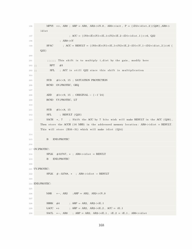
196 MPYS ∗+, AR0 ; ARP = AR0, AR2−>iN 0 , AR3−>i n i t , P = ( iD2∗ i d i s t 2 ) (Q28) ,AR0−>
i d i s t
197 ; ACC = ( iN0∗ iE+iN1∗ iE 1+iN2∗ iE 2−iD1∗ i d i s t 1 )>>6, Q22
198 ; AR0−>iY
199 SPAC ; ACC = RESULT = ( iN0∗ iE+iN1∗ iE 1+iN2∗ iE 2−iD1∗ iY 1−iD2∗ i d i s t 2 )>>6 (
Q22)
200
201 ; ; ; ; ; ; This s h i f t i s to mult ip ly i d i s t by the gain , modify here
202 ; ; RPT #3
203 ; ; SFL ; ACC i s s t i l l Q22 s i n c e t h i s s h i f t i s mu l t i p l i c a t i o n
204
205 SUB #1<<8, 15 ; SATUATION PROTECTION
206 BCND OVPROTEC, GEQ
207
208 ADD #1<<9, 15 ; ORIGINAL − (−1ˆ24)
209 BCND UV PROTEC, LT
210
211 SUB #1<<8, 15
212 SFL ; RESULT (Q23)
213 SACH ∗ , 7 ; S h i f t the ACC by 7 b i t s wish w i l l make RESULT in the ACC (Q30) ,
Then s t o r e the ACCH (16 MSB) in the addressed memory l o c a t i o n : AR0−> i d i s t = RESULT.
This w i l l s t o r e (B16−31) which w i l l make i d i s t (Q14)
214
215 B ENDPROTEC
216
217 OVPROTEC:
218 SPLK #32767 , ∗ ; AR0−> i d i s t = RESULT
219 B ENDPROTEC
220
221 UVPROTEC:
222 SPLK #−32768, ∗ ; AR0−> i d i s t = RESULT
223
224 ENDPROTEC:
225
226 MAR ∗−, AR2 ;ARP = AR2, AR2−>iN 0
227
228 SBRK #4 ; ARP = AR2, AR2−>iE 1
229 LACC ∗+ ; ARP = AR2, AR2−>iE 2 , ACC = iE 1
230 SACL ∗−, AR0 ; ARP = AR2, AR2−>iE 1 , iE 2 = iE 1 , AR0−> i d i s t
168

231 ;MAR ∗− ; AR0−>iE
232 LACC ∗+, AR2 ; ARP = AR2, AR2−>iE 1 , ACC = iE , AR0−> i d i s t
233 SACL ∗+ ; ARP = AR2, AR2−>iE 2 , iE 1 = iE , AR0−> i d i s t
234 MAR ∗+ ; ARP = AR2, AR2−> i d i s t 1
235 LACC ∗+ ; ARP = AR2, AR2−>i d i s t 2 , ACC = i d i s t 1
236 SACL ∗−, AR0 ; ARP = AR0, AR2−>i d i s t 1 , i d i s t 2 = i d i s t 1
237 LACC ∗ , AR2 ; ARP = AR2, AR2−>i d i s t 1 , ACC = i d i s t
238 SACL ∗ ,AR1 ; ARP = AR1, AR2−>iE 1 , i d i s t 1 = i d i s t , AR0−> i d i s t
239
240
241
242 d i s tE s tC a l c e x i t :
243
244 CLRC OVM
245 SPM 0
246
247 ; MAR ∗ ,AR1 ; can be removed i f t h i s cond i t i on i s met on
248 ; every path to t h i s code .
249 ; s e t ARP = SP be f o r e you e x i t .
250 SBRK #( d i s tE s tCa l c f r ame s i z e +1)
251 ; d e a l l o c a t e frame , po int to saved FP
252 LAR AR0, ∗− ; r e s t o r e frame po in t e r
253 PSHD ∗ ; push re turn address on hardware s tack
254
255 RET
256
257 . end
Code for the Grid-Connected 1φ VS DC-AC PEC with
LCL-Type Filter
Current Controller Header File Code
1 /∗ ==============================================================================
2 System Name : S i ng l e phase i n v e r t e r cur r ent c on t r o l
3
4 F i l e Name : i n v1 cn t l 2 . h
169
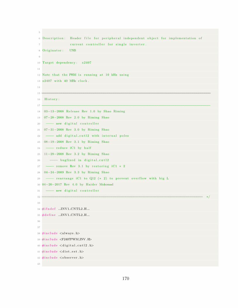
5
6 Desc r ip t i on : Header f i l e f o r p e r i ph e r a l independent ob j e c t f o r implementation o f
7 cur rent c o n t r o l l e r f o r s i n g l e i n v e r t e r .
8 Or ig inato r : UNB
9
10 Target dependency : x2407
11
12 Note that the PWM i s running at 10 kHz us ing
13 x2407 with 40 MHz c lock .
14
15 =====================================================================================
16 History :
17 −−−−−−−−−−−−−−−−−−−−−−−−−−−−−−−−−−−−−−−−−−−−−−−−−−−−−−−−−−−−−−−−−−−−−−−−−−−−−−−−−−−−−
18 03−13−2008 Release Rev 1 .0 by Shao Riming
19 07−28−2008 Rev 2 .0 by Riming Shao
20 −−−− new d i g i t a l c o n t r o l l e r
21 07−31−2008 Rev 3 .0 by Riming Shao
22 −−−− add d i g i t a l c n t l 2 with i n t e r n a l po l e s
23 08−19−2008 Rev 3 .1 by Riming Shao
24 −−−− reduce iC1 by ha l f
25 11−29−2008 Rev 3 .2 by Riming Shao
26 −−−− bugf ixed in d i g i t a l c n t l 2
27 −−−− remove Rev 3 .1 by r e s t o r i n g iC1 ∗ 2
28 04−24−2009 Rev 3 .3 by Riming Shao
29 −−−− r ea r range iC1 to Q12 (∗ 2) to prevent over f l ow with big L
30 04−20−2017 Rev 4 .0 by Haider Mohomad
31 −−−− new d i g i t a l c o n t r o l l e r
32 ================================================================================= ∗/
33
34 #i f n d e f INV1 CNTL2 H
35 #de f i n e INV1 CNTL2 H
36
37
38 #inc lude <always . h>
39 #inc lude <F2407PWM INV.H>
40 #inc lude <d i g i t a l c n t l 2 . h>
41 #inc lude <d i s t e s t . h>
42 #inc lude <obse rve r . h>
43
170
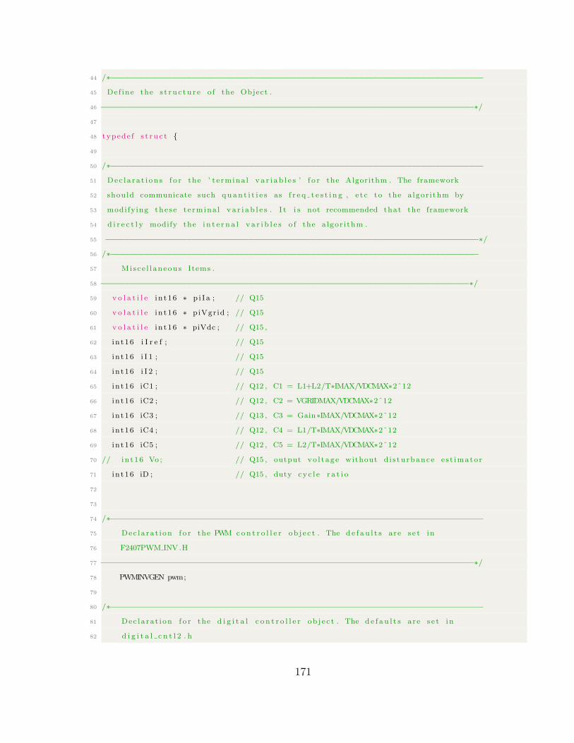
44 /∗−−−−−−−−−−−−−−−−−−−−−−−−−−−−−−−−−−−−−−−−−−−−−−−−−−−−−−−−−−−−−−−−−−−−−−−−−−−−−−
45 Def ine the s t r u c tu r e o f the Object .
46 −−−−−−−−−−−−−−−−−−−−−−−−−−−−−−−−−−−−−−−−−−−−−−−−−−−−−−−−−−−−−−−−−−−−−−−−−−−−−−∗/
47
48 typede f s t r u c t
49
50 /∗−−−−−−−−−−−−−−−−−−−−−−−−−−−−−−−−−−−−−−−−−−−−−−−−−−−−−−−−−−−−−−−−−−−−−−−−−−−−−−
51 Dec l a ra t i on s f o r the ’ t e rmina l v a r i a b l e s ’ f o r the Algorithm . The framework
52 should communicate such quan t i t i e s as f r e q t e s t i n g , e t c to the a lgor i thm by
53 modifying these te rmina l v a r i a b l e s . I t i s not recommended that the framework
54 d i r e c t l y modify the i n t e r n a l v a r i b l e s o f the a lgor i thm .
55 −−−−−−−−−−−−−−−−−−−−−−−−−−−−−−−−−−−−−−−−−−−−−−−−−−−−−−−−−−−−−−−−−−−−−−−−−−−−−−∗/
56 /∗−−−−−−−−−−−−−−−−−−−−−−−−−−−−−−−−−−−−−−−−−−−−−−−−−−−−−−−−−−−−−−−−−−−−−−−−−−−−−
57 Misce l l aneous Items .
58 −−−−−−−−−−−−−−−−−−−−−−−−−−−−−−−−−−−−−−−−−−−−−−−−−−−−−−−−−−−−−−−−−−−−−−−−−−−−−∗/
59 v o l a t i l e in t16 ∗ p i I a ; // Q15
60 v o l a t i l e in t16 ∗ piVgr id ; // Q15
61 v o l a t i l e in t16 ∗ piVdc ; // Q15 ,
62 i n t16 i I r e f ; // Q15
63 i n t16 i I 1 ; // Q15
64 i n t16 i I 2 ; // Q15
65 i n t16 iC1 ; // Q12 , C1 = L1+L2/T∗IMAX/VDCMAX∗2ˆ12
66 i n t16 iC2 ; // Q12 , C2 = VGRIDMAX/VDCMAX∗2ˆ12
67 i n t16 iC3 ; // Q13 , C3 = Gain∗IMAX/VDCMAX∗2ˆ12
68 i n t16 iC4 ; // Q12 , C4 = L1/T∗IMAX/VDCMAX∗2ˆ12
69 i n t16 iC5 ; // Q12 , C5 = L2/T∗IMAX/VDCMAX∗2ˆ12
70 // in t16 Vo ; // Q15 , output vo l t age without d i s turbance e s t imator
71 i n t16 iD ; // Q15 , duty cy c l e r a t i o
72
73
74 /∗−−−−−−−−−−−−−−−−−−−−−−−−−−−−−−−−−−−−−−−−−−−−−−−−−−−−−−−−−−−−−−−−−−−−−−−−−−−−−−
75 Dec la ra t i on f o r the PWM con t r o l l e r ob j e c t . The d e f a u l t s are s e t in
76 F2407PWM INV.H
77 −−−−−−−−−−−−−−−−−−−−−−−−−−−−−−−−−−−−−−−−−−−−−−−−−−−−−−−−−−−−−−−−−−−−−−−−−−−−−−∗/
78 PWMINVGEN pwm;
79
80 /∗−−−−−−−−−−−−−−−−−−−−−−−−−−−−−−−−−−−−−−−−−−−−−−−−−−−−−−−−−−−−−−−−−−−−−−−−−−−−−−
81 Dec la ra t i on f o r the d i g i t a l c o n t r o l l e r ob j e c t . The d e f a u l t s are s e t in
82 d i g i t a l c n t l 2 . h
171

83 −−−−−−−−−−−−−−−−−−−−−−−−−−−−−−−−−−−−−−−−−−−−−−−−−−−−−−−−−−−−−−−−−−−−−−−−−−−−−−∗/
84 // DIGITAL CNTL2 d i g i t c n t l 2 ;
85 DIST EST d i s t e s t ;
86
87 // Observer
88 OBSERVER obse rve r ;
89
90 /∗−−−−−−−−−−−−−−−−−−−−−−−−−−−−−−−−−−−−−−−−−−−−−−−−−−−−−−−−−−−−−−−−−−−−−−−−−−−−−−
91 Dec la ra t i on f o r the f unc t i on s implemented in i nv1 cn t l 2 . c
92 −−−−−−−−−−−−−−−−−−−−−−−−−−−−−−−−−−−−−−−−−−−−−−−−−−−−−−−−−−−−−−−−−−−−−−−−−−−−−−∗/
93 void (∗ i n i t ) ( ) ; // po in t e r to a func t i on
94 void (∗ update ) ( ) ;
95 void (∗ d i s ab l e ) ( ) ;
96 void (∗ enable ) ( ) ;
97
98 INV1 CNTL2 ;
99
100
101 #de f i n e INV1 CNTL2 INITVALS \
102 \
103 ( in t16 ∗) 0 , \
104 ( in t16 ∗) 0 , \
105 ( in t16 ∗) 0 , \
106 0 , \
107 0 , \
108 0 , \
109 0 , \
110 0 , \
111 0 , \
112 0 , \
113 0 , \
114 0 , \
115 PWMINVGENDEFAULTS, \
116 DIST EST INITVALS , \
117 OBSERVER INITVALS, \
118 ( void (∗ ) ( ) ) inv1Cnt l2 In i t , \
119 ( void (∗ ) ( ) ) inv1Cntl2Update , \
120 ( void (∗ ) ( ) ) inv1Cnt l2Disable , \
121 ( void (∗ ) ( ) ) inv1Cntl2Enable \
172
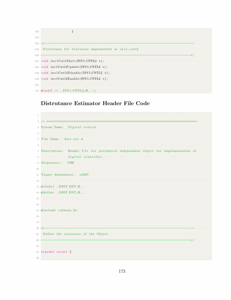
122
123
124 /∗−−−−−−−−−−−−−−−−−−−−−−−−−−−−−−−−−−−−−−−−−−−−−−−−−−−−−−−−−−−−−−−−−−−−−−−−−−−−−−
125 Prototypes f o r f un c t i on s implemented in i nv1 cn t l 2
126 −−−−−−−−−−−−−−−−−−−−−−−−−−−−−−−−−−−−−−−−−−−−−−−−−−−−−−−−−−−−−−−−−−−−−−−−−−−−−−∗/
127 void inv1Cnt l 2 In i t (INV1 CNTL2 ∗) ;
128 void inv1Cntl2Update (INV1 CNTL2 ∗) ;
129 void inv1Cnt l2Disab le (INV1 CNTL2 ∗) ;
130 void inv1Cntl2Enable (INV1 CNTL2 ∗) ;
131
132 #end i f /∗ INV1 CNTL2 H ∗/
Distrutance Estimator Header File Code
1
2 /∗ ==============================================================================
3 System Name : D i g i t a l c on t r o l
4
5 F i l e Name : d i s t e s t . h
6
7 Desc r ip t i on : Header f i l e f o r p e r i ph e r a l independent ob j e c t f o r implementation o f
8 d i g i t a l c o n t r o l l e r .
9 Or ig inato r : UNB
10
11 Target dependency : x2407
12
13 #i f n d e f DIST EST H
14 #de f i n e DIST EST H
15
16
17 #inc lude <always . h>
18
19
20 /∗−−−−−−−−−−−−−−−−−−−−−−−−−−−−−−−−−−−−−−−−−−−−−−−−−−−−−−−−−−−−−−−−−−−−−−−−−−−−−−
21 Def ine the s t r u c tu r e o f the Object .
22 −−−−−−−−−−−−−−−−−−−−−−−−−−−−−−−−−−−−−−−−−−−−−−−−−−−−−−−−−−−−−−−−−−−−−−−−−−−−−−∗/
23
24 typede f s t r u c t
25
173
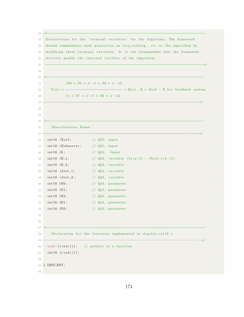
26 /∗−−−−−−−−−−−−−−−−−−−−−−−−−−−−−−−−−−−−−−−−−−−−−−−−−−−−−−−−−−−−−−−−−−−−−−−−−−−−−−
27 Dec l a ra t i on s f o r the ’ t e rmina l v a r i a b l e s ’ f o r the Algorithm . The framework
28 should communicate such quan t i t i e s as f r e q t e s t i n g , e t c to the a lgor i thm by
29 modifying these te rmina l v a r i a b l e s . I t i s not recommended that the framework
30 d i r e c t l y modify the i n t e r n a l v a r i b l e s o f the a lgor i thm .
31 −−−−−−−−−−−−−−−−−−−−−−−−−−−−−−−−−−−−−−−−−−−−−−−−−−−−−−−−−−−−−−−−−−−−−−−−−−−−−−∗/
32
33 /∗−−−−−−−−−−−−−−−−−−−−−−−−−−−−−−−−−−−−−−−−−−−−−−−−−−−−−−−−−−−−−−−−−−−−−−−−−−−−−
34 (N0 + N1 ∗ zˆ−1 + N2 ∗ zˆ−2)
35 Y( z ) = −−−−−−−−−−−−−−−−−−−−−−−−−−−− ∗ E( z ) , E = Xref − X fo r feedback system
36 (1 + D1 ∗ zˆ−1 + D2 ∗ zˆ−2)
37 −−−−−−−−−−−−−−−−−−−−−−−−−−−−−−−−−−−−−−−−−−−−−−−−−−−−−−−−−−−−−−−−−−−−−−−−−−−−−∗/
38
39
40 /∗−−−−−−−−−−−−−−−−−−−−−−−−−−−−−−−−−−−−−−−−−−−−−−−−−−−−−−−−−−−−−−−−−−−−−−−−−−−−−
41 Misce l l aneous Items .
42 −−−−−−−−−−−−−−−−−−−−−−−−−−−−−−−−−−−−−−−−−−−−−−−−−−−−−−−−−−−−−−−−−−−−−−−−−−−−−∗/
43 i n t16 iXr e f ; // Q15 , input
44 i n t16 iXobserver ; // Q15 , input
45 i n t16 iX ; // Q15 , Input
46 i n t16 iE 1 ; // Q14 , v a r i ab l e ( Ix [ n−1] − iX r e f 1 [ n−1])
47 i n t16 iE 2 ; // Q14 , v a r i ab l e
48 i n t16 i d i s t 1 ; // Q14 , v a r i ab l e
49 i n t16 i d i s t 2 ; // Q14 , v a r i ab l e
50 i n t16 iN0 ; // Q14 , parameter
51 i n t16 iN1 ; // Q14 , parameter
52 i n t16 iN2 ; // Q14 , parameter
53 i n t16 iD1 ; // Q14 , parameter
54 i n t16 iD2 ; // Q14 , parameter
55
56
57 /∗−−−−−−−−−−−−−−−−−−−−−−−−−−−−−−−−−−−−−−−−−−−−−−−−−−−−−−−−−−−−−−−−−−−−−−−−−−−−−−
58 Dec la ra t i on f o r the f unc t i on s implemented in d i g i t a l c n t l 2 . c
59 −−−−−−−−−−−−−−−−−−−−−−−−−−−−−−−−−−−−−−−−−−−−−−−−−−−−−−−−−−−−−−−−−−−−−−−−−−−−−−∗/
60 void (∗ i n i t ) ( ) ; // po in t e r to a func t i on
61 i n t16 (∗ c a l c ) ( ) ;
62
63 DIST EST ;
64
174

65
66 #de f i n e DIST EST INITVALS \
67 \
68 0 , \
69 0 , \
70 0 , \
71 0 , \
72 0 , \
73 0 , \
74 0 , \
75 0 , \
76 0 , \
77 0 , \
78 0 , \
79 0 , \
80 ( void (∗ ) ( ) ) d i s tE s t I n i t , \
81 ( in t16 (∗ ) ( ) ) d i s tEs tCa l c \
82
83
84 /∗−−−−−−−−−−−−−−−−−−−−−−−−−−−−−−−−−−−−−−−−−−−−−−−−−−−−−−−−−−−−−−−−−−−−−−−−−−−−−−
85 Prototypes f o r f un c t i on s implemented in d i g i t a l c n t l 2 . c or d i g i t a l c n t l 2 a . asm
86 −−−−−−−−−−−−−−−−−−−−−−−−−−−−−−−−−−−−−−−−−−−−−−−−−−−−−−−−−−−−−−−−−−−−−−−−−−−−−−∗/
87 void d i s t E s t I n i t (DIST EST ∗) ;
88 i n t16 d i s tEs tCa l c (DIST EST ∗) ;
89
90 #end i f /∗ DIST EST H ∗/
Observer Header File Code
1 /∗ ==============================================================================
2 System Name : Observer
3
4 F i l e Name : obse rve r . h
5
6 Desc r ip t i on : Header f i l e f o r p e r i ph e r a l independent ob j e c t f o r implementation o f
7 d i g i t a l c o n t r o l l e r .
8 Or ig inato r : UNB
9
10 Target dependency : x2407
175

11
12 #i f n d e f OBSERVER H
13 #de f i n e OBSERVER H
14
15
16 #inc lude <always . h>
17
18
19 /∗−−−−−−−−−−−−−−−−−−−−−−−−−−−−−−−−−−−−−−−−−−−−−−−−−−−−−−−−−−−−−−−−−−−−−−−−−−−−−−
20 Def ine the s t r u c tu r e o f the Object .
21 −−−−−−−−−−−−−−−−−−−−−−−−−−−−−−−−−−−−−−−−−−−−−−−−−−−−−−−−−−−−−−−−−−−−−−−−−−−−−−∗/
22
23 typede f s t r u c t
24
25 /∗−−−−−−−−−−−−−−−−−−−−−−−−−−−−−−−−−−−−−−−−−−−−−−−−−−−−−−−−−−−−−−−−−−−−−−−−−−−−−−
26 Dec l a ra t i on s f o r the ’ t e rmina l v a r i a b l e s ’ f o r the Algorithm . The framework
27 should communicate such quan t i t i e s as f r e q t e s t i n g , e t c to the a lgor i thm by
28 modifying these te rmina l v a r i a b l e s . I t i s not recommended that the framework
29 d i r e c t l y modify the i n t e r n a l v a r i b l e s o f the a lgor i thm .
30 −−−−−−−−−−−−−−−−−−−−−−−−−−−−−−−−−−−−−−−−−−−−−−−−−−−−−−−−−−−−−−−−−−−−−−−−−−−−−−∗/
31
32 /∗−−−−−−−−−−−−−−−−−−−−−−−−−−−−−−−−−−−−−−−−−−−−−−−−−−−−−−−−−−−−−−−−−−−−−−−−−−−−−
33 Misce l l aneous Items .
34 −−−−−−−−−−−−−−−−−−−−−−−−−−−−−−−−−−−−−−−−−−−−−−−−−−−−−−−−−−−−−−−−−−−−−−−−−−−−−∗/
35 i n t16 iL1 1 ; // Q15 , input IL1 [ n−1]
36 i n t16 iL2 1 ; // Q15 , input IL2 [ n−1]
37 i n t16 Vc 1 ; // Q15 , input Vc [ n−1]
38 i n t16 Vo 1 ; // Q15 , input Vo [ n−1]
39 i n t16 Vg 1 ; // Q15 , input Vg [ n−1]
40 i n t16 A11 ; // Q12 , A11 =??? a11∗IMAX/VDCMAX∗2ˆ12
41 i n t16 A12 ; // Q12 , A12 =??? a12∗VGRIDMAX/VDCMAX∗2ˆ12
42 i n t16 A13 ; // Q12 , A12 =??? a12∗VGRIDMAX/VDCMAX∗2ˆ12
43 i n t16 B11 ; // Q12 , A12 =??? a12∗VGRIDMAX/VDCMAX∗2ˆ12
44 i n t16 B12 ; // Q12 , A12 =??? a12∗VGRIDMAX/VDCMAX∗2ˆ12
45 i n t16 A21 ; // Q12 , A11 =??? a11∗IMAX/VDCMAX∗2ˆ12
46 i n t16 A22 ; // Q12 , A12 =??? a12∗VGRIDMAX/VDCMAX∗2ˆ12
47 i n t16 A23 ; // Q12 , A12 =??? a12∗VGRIDMAX/VDCMAX∗2ˆ12
48 i n t16 B21 ; // Q12 , A12 =??? a12∗VGRIDMAX/VDCMAX∗2ˆ12
49 i n t16 B22 ; // Q12 , A12 =??? a12∗VGRIDMAX/VDCMAX∗2ˆ12
176

50 i n t16 A31 ; // Q12 , A11 =??? a11∗IMAX/VDCMAX∗2ˆ12
51 i n t16 A32 ; // Q12 , A12 =??? a12∗VGRIDMAX/VDCMAX∗2ˆ12
52 i n t16 A33 ; // Q12 , A12 =??? a12∗VGRIDMAX/VDCMAX∗2ˆ12
53 i n t16 B31 ; // Q12 , A12 =??? a12∗VGRIDMAX/VDCMAX∗2ˆ12
54 i n t16 B32 ; // Q12 , A12 =??? a12∗VGRIDMAX/VDCMAX∗2ˆ1
55
56
57 /∗−−−−−−−−−−−−−−−−−−−−−−−−−−−−−−−−−−−−−−−−−−−−−−−−−−−−−−−−−−−−−−−−−−−−−−−−−−−−−−
58 Dec la ra t i on f o r the f unc t i on s implemented in d i g i t a l c n t l 2 . c
59 −−−−−−−−−−−−−−−−−−−−−−−−−−−−−−−−−−−−−−−−−−−−−−−−−−−−−−−−−−−−−−−−−−−−−−−−−−−−−−∗/
60 void (∗ i n i t ) ( ) ; // po in t e r to a func t i on
61 i n t16 (∗ c a l c ) ( ) ;
62
63 OBSERVER;
64
65
66 #de f i n e OBSERVER INITVALS \
67 \
68 0 , \
69 0 , \
70 0 , \
71 0 , \
72 0 , \
73 0 , \
74 0 , \
75 0 , \
76 0 , \
77 0 , \
78 0 , \
79 0 , \
80 0 , \
81 0 , \
82 0 , \
83 0 , \
84 0 , \
85 0 , \
86 0 , \
87 0 , \
88 ( void (∗ ) ( ) ) ob s e r v e r I n i t , \
177

89 ( in t16 (∗ ) ( ) ) observerCa lc \
90
91
92 /∗−−−−−−−−−−−−−−−−−−−−−−−−−−−−−−−−−−−−−−−−−−−−−−−−−−−−−−−−−−−−−−−−−−−−−−−−−−−−−−
93 Prototypes f o r f un c t i on s implemented in d i g i t a l c n t l 2 . c or d i g i t a l c n t l 2 a . asm
94 −−−−−−−−−−−−−−−−−−−−−−−−−−−−−−−−−−−−−−−−−−−−−−−−−−−−−−−−−−−−−−−−−−−−−−−−−−−−−−∗/
95 void ob s e r v e r I n i t (DIST EST ∗) ;
96 i n t16 observerCa lc (DIST EST ∗) ;
97
98 #end i f /∗ DIST EST H ∗/
Current Controller Assembly Code
1 ; /∗ ==============================================================================
2 ; System Name : S i ng l e phase i n v e r t e r
3
4 ; F i l e Name : i n v 1 cn t l 2 a . asm
5
6 ; De s c r ip t i on : implementation o f cur r ent c on t r o l f o r s i n g l e phase i n v e r t e r .
7 ; Or i g ina to r : UNB
8
9 ; Target dependency : x2407
10 ;=====================================================================================
11 ; H i s tory :
12 ;−−−−−−−−−−−−−−−−−−−−−−−−−−−−−−−−−−−−−−−−−−−−−−−−−−−−−−−−−−−−−−−−−−−−−−−−−−−−−−−−−−−−−
13 ; 03−14−2008 Release Rev 1 .0 by Shao Riming
14 ; 07−28−2008 Rev 2 .0 by Riming Shao
15 ; −−−− new d i g i t a l c o n t r o l l e r
16 ; 07−31−2008 Rev 3 .0 by Riming Shao
17 ; −−−− add d i g i t a l c n t l 2 with i n t e r n a l po l e s
18 ; 08−19−2008 Rev 3 .1 by Riming Shao
19 ; −−−− reduce iC1 by ha l f
20 ; 11−29−2008 Rev 3 .2 by Riming Shao
21 ; −−−− bugf ixed in d i g i t a l c n t l 2
22 ; −−−− remove Rev 3 .1 by r e s t o r i n g iC1 ∗ 2
23 ; 04−24−2009 Rev 3 .3 by Riming Shao
24 ; −−−− r ea r range iC1 to Q12 (∗ 2) to prevent over f l ow with big L
25 ; 12−05−2017 Rev 4 .0 by Haider Mohomad
26 ; −−−− new d i g i t a l c o n t r o l l e r
178

27 ;================================================================================= ∗/
28
29 ;================================================================================
30 ; Routine Name : INV1 CNTL2 Routine Type : C Ca l l ab l e
31 ;
32 ; De s c r ip t i on :
33 ;
34 ; C prototype : void inv1Cntl2Update (INV1 CNTL2 ∗p) ;
35 ; H i s tory c rea ted July 31 , 2008
36 ;================================================================================
37 ; D e f i n i t i o n o f INV1 CNTL2
38 ; /∗−−−−−−−−−−−−−−−−−−−−−−−−−−−−−−−−−−−−−−−−−−−−−−−−−−−−−−−−−−−−−−−−−−−−−−−−−−−−−−
39 ; Def ine the s t r u c tu r e o f the Object .
40 ;−−−−−−−−−−−−−−−−−−−−−−−−−−−−−−−−−−−−−−−−−−−−−−−−−−−−−−−−−−−−−−−−−−−−−−−−−−−−−−∗/
41 ;
42 ; typede f s t r u c t
43 ;
44 ; /∗−−−−−−−−−−−−−−−−−−−−−−−−−−−−−−−−−−−−−−−−−−−−−−−−−−−−−−−−−−−−−−−−−−−−−−−−−−−−−−
45 ; Dec l a ra t i on s f o r the ’ t e rmina l v a r i a b l e s ’ f o r the Algorithm . The framework
46 ; should communicate such quan t i t i e s as f r e q t e s t i n g , e t c to the a lgor i thm by
47 ; modifying these te rmina l v a r i a b l e s . I t i s not recommended that the framework
48 ; d i r e c t l y modify the i n t e r n a l v a r i b l e s o f the a lgor i thm .
49 ; −−−−−−−−−−−−−−−−−−−−−−−−−−−−−−−−−−−−−−−−−−−−−−−−−−−−−−−−−−−−−−−−−−−−−−−−−−−−−−∗/
50 ; /∗−−−−−−−−−−−−−−−−−−−−−−−−−−−−−−−−−−−−−−−−−−−−−−−−−−−−−−−−−−−−−−−−−−−−−−−−−−−−−
51 ; Mi s ce l l aneous Items .
52 ;−−−−−−−−−−−−−−−−−−−−−−−−−−−−−−−−−−−−−−−−−−−−−−−−−−−−−−−−−−−−−−−−−−−−−−−−−−−−−∗/
53 ; v o l a t i l e in t16 ∗ p i I a ; // Q15
54 ; v o l a t i l e in t16 ∗ piVgr id ; // Q15
55 ; v o l a t i l e in t16 ∗ piVdc ; // Q15 ,
56 ; i n t16 i I r e f ; // Q15 ;
57 ; i n t16 i I 1 o b s e r v e r ; // Q15
58 ; i n t16 i I 2 o b s e r v e r ; // Q15
59 ; i n t16 iC1 ; // Q12 , C1 = L1+L2/T∗IMAX/VDCMAX∗2ˆ12
60 ; i n t16 iC2 ; // Q12 , C2 = VGRIDMAX/VDCMAX∗2ˆ12
61 ; i n t16 iC3 ; // Q13 , C3 = Gain∗IMAX/VDCMAX∗2ˆ12
62 ; i n t16 iC4 ; // Q12 , C4 = L1/T∗IMAX/VDCMAX∗2ˆ12
63 ; i n t16 iC5 ; // Q12 , C5 = L2/T∗IMAX/VDCMAX∗2ˆ12
64 ; i n t16 iD ; // Q15 , duty cy c l e r a t i o
65
179
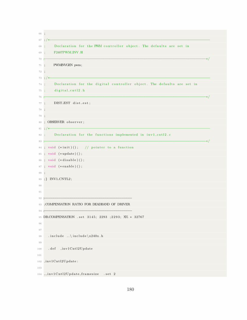
66 ;
67 ; /∗−−−−−−−−−−−−−−−−−−−−−−−−−−−−−−−−−−−−−−−−−−−−−−−−−−−−−−−−−−−−−−−−−−−−−−−−−−−−−−
68 ; Dec la ra t i on f o r the PWM con t r o l l e r ob j e c t . The d e f a u l t s are s e t in
69 ; F2407PWM INV.H
70 ;−−−−−−−−−−−−−−−−−−−−−−−−−−−−−−−−−−−−−−−−−−−−−−−−−−−−−−−−−−−−−−−−−−−−−−−−−−−−−−∗/
71 ; PWMINVGEN pwm;
72 ;
73 ; /∗−−−−−−−−−−−−−−−−−−−−−−−−−−−−−−−−−−−−−−−−−−−−−−−−−−−−−−−−−−−−−−−−−−−−−−−−−−−−−−
74 ; Dec la ra t i on f o r the d i g i t a l c o n t r o l l e r ob j e c t . The d e f a u l t s are s e t in
75 ; d i g i t a l c n t l 2 . h
76 ;−−−−−−−−−−−−−−−−−−−−−−−−−−−−−−−−−−−−−−−−−−−−−−−−−−−−−−−−−−−−−−−−−−−−−−−−−−−−−−∗/
77 ; DIST EST d i s t e s t ;
78 ;
79 ;
80 ; OBSERVER obse rve r ;
81 ; /∗−−−−−−−−−−−−−−−−−−−−−−−−−−−−−−−−−−−−−−−−−−−−−−−−−−−−−−−−−−−−−−−−−−−−−−−−−−−−−−
82 ; Dec la ra t i on f o r the f unc t i on s implemented in i nv1 cn t l 2 . c
83 ;−−−−−−−−−−−−−−−−−−−−−−−−−−−−−−−−−−−−−−−−−−−−−−−−−−−−−−−−−−−−−−−−−−−−−−−−−−−−−−∗/
84 ; void (∗ i n i t ) ( ) ; // po in t e r to a func t i on
85 ; void (∗ update ) ( ) ;
86 ; void (∗ d i s ab l e ) ( ) ;
87 ; void (∗ enable ) ( ) ;
88 ;
89 ; INV1 CNTL2 ;
90
91
92 ;−−−−−−−−−−−−−−−−−−−−−−−−−−−−−−−−−−−−−−−−−−
93 ;COMPENSATION RATIO FOR DEADBAND OF DRIVER
94 ;−−−−−−−−−−−−−−−−−−−−−−−−−−−−−−−−−−−−−−−−−−
95 DBCOMPENSATION . s e t 3145 ; 2293 ; 2 2 9 3 ; X% ∗ 32767
96
97
98 . i n c lude . . \ i n c lude \x240x . h
99
100 . de f inv1Cntl2Update
101
102 inv1Cntl2Update :
103
104 i nv1Cnt l2Update f rames i z e . s e t 2
180
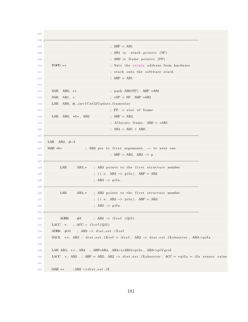
105
106 ;−−−−−−−−−−−−−−−−−−−−−−−−−−−−−−−−−−−−−−−−−−−−−−−−−−−−−−−−−−−−−−−−−−−−−−−−−−
107 ; ARP = AR1
108 ; AR1 i s s tack po in t e r (SP)
109 ; AR0 i s frame po in t e r (FP)
110 POPD ∗+ ; Save the re turn address from hardware
111 ; s tack onto the so f tware s tack
112 ; ARP = AR1
113
114 SAR AR0, ∗+ ; push AR0(FP) . ARP =AR1
115 SAR AR1, ∗ ; ∗SP = SP . ARP =AR1
116 LAR AR0, # inv1Cnt l2Update f rames i z e
117 ; FP = s i z e o f frame
118 LAR AR0, ∗0+, AR2 ; ARP = AR2.
119 ; A l l o ca t e frame . AR0 = ∗AR1
120 ; AR1 = AR1 + AR0.
121 ;−−−−−−−−−−−−−−−−−−−−−−−−−−−−−−−−−−−−−−−−−−−−−−−−−−−−−−−−−−−−−−−−−−−−−−−−−−
122 LAR AR2, #−3
123 MAR ∗0+ ; AR2 pts to f i r s t arguments , −− to next one
124 ; ARP = AR2, AR2 −> p
125 ;−−−−−−−−−−−−−−−−−−−−−−−−−−−−−−−−−−−−−−−−−−−−−−−−−−−−−−−−−−−−−−−−−−−−−−−−−−
126 LAR AR3,∗ ; AR3 po in t s to the f i r s t s t r u c tu r e member
127 ; ( i . e . AR3 −> p i I a ) . ARP = AR2
128 ; AR3 −> p i I a .
129 ;−−−−−−−−−−−−−−−−−−−−−−−−−−−−−−−−−−−−−−−−−−−−−−−−−−−−−−−−−−−−−−−−−−−−−−−−−−
130 LAR AR2,∗ ; AR2 po in t s to the f i r s t s t r u c tu r e member
131 ; ( i . e . AR2 −> p i I a ) . ARP = AR2.
132 ; AR2 −> p i I a .
133 ;−−−−−−−−−−−−−−−−−−−−−−−−−−−−−−−−−−−−−−−−−−−−−−−−−−−−−−−−−−−−−−−−−−−−−−−−−−
134 ADRK #3 ; AR2 −> i I r e f (Q15)
135 LACC ∗ ; ACC = i I r e f (Q15)
136 ADRK #14 ; AR2 −> d i s t e s t . iX r e f
137 SACL ∗+, AR3 ; d i s t e s t . iX r e f = i I r e f , AR2 −> d i s t e s t . iXobserver , AR3−>p i I a
138
139 LAR AR4, ∗+, AR4 ; ARP=AR4, AR4=(∗AR3)=piIa , AR3−>piVgr id
140 LACC ∗ , AR2 ; ARP = AR2, AR2 −> d i s t e s t . iXobserver , ACC = ∗ p i I a = i I a s enso r va lue
141
142 MAR ∗+ ;AR2 −>d i s t e s t . iX
181
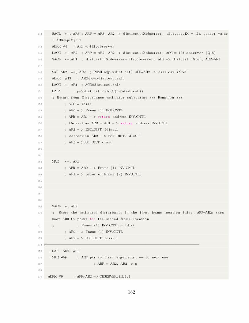
143 SACL ∗−, AR3 ; ARP = AR3, AR2 −> d i s t e s t . iXobserver , d i s t e s t . iX = i I a s enso r value
, AR3−>piVgr id
144 ADRK #4 ; AR3 −> i I 2 o b s e r v e r
145 LACC ∗ , AR2 ; ARP = AR2, AR2 −> d i s t e s t . iXobserver , ACC = i I 2 o b s e r v e r (Q15)
146 SACL ∗−,AR1 ; d i s t e s t . iXobserver= i I 2 ob s e r v e r , AR2 −> d i s t e s t . iXre f , ARP=AR1
147
148 SAR AR2, ∗+, AR2 ; PUSH &(p−>d i s t e s t ) APR=AR2 −> d i s t e s t . iX r e f
149 ADRK #13 ; AR2−>p−>d i s t e s t . c a l c
150 LACC ∗ , AR1 ; ACC=d i s t e s t . c a l c
151 CALA ; p−>d i s t e s t . c a l c (&(p−>d i s t e s t ) )
152 ; Return from Disturbance e s t imator subrout ine ∗∗∗ Remember ∗∗∗
153 ; ACC = i d i s t
154 ; AR0 − > Frame (1) INV CNTL
155 ; APR = AR1 − > r e turn address INV CNTL
156 ; Cor rec t ion APR = AR1 − > r e turn address INV CNTL
157 ; AR2 − > EST DIST . I d i s t 1
158 ; c o r r e c t i o n AR2 − > EST DIST . I d i s t 1
159 ; AR3 − >EST DIST .∗ i n i t
160
161
162 MAR ∗−, AR0
163 ; APR = AR0 − > Frame (1) INV CNTL
164 ; AR1 − > below o f Frame (2) INV CNTL
165
166
167
168
169 SACL ∗ , AR2
170 ; Store the est imated d i s turbance in the f i r s t frame l o c a t i o n i d i s t , ARP=AR2; then
move AR0 to po int f o r the second frame l o c a t i o n
171 ; ; Frame (1) INV CNTL = i d i s t
172 ; AR0 − > Frame (1) INV CNTL
173 ; AR2 − > EST DIST . I d i s t 1
174 ;−−−−−−−−−−−−−−−−−−−−−−−−−−−−−−−−−−−−−−−−−−−−−−−−−−−−−−−−−−−−−−−−−−−−−−−−−−
175 ; LAR AR2, #−3
176 ; MAR ∗0+ ; AR2 pts to f i r s t arguments , −− to next one
177 ; ARP = AR2, AR2 −> p
178
179 ADRK #9 ; APR=AR2 −> OBSERVER. i IL1 1
182
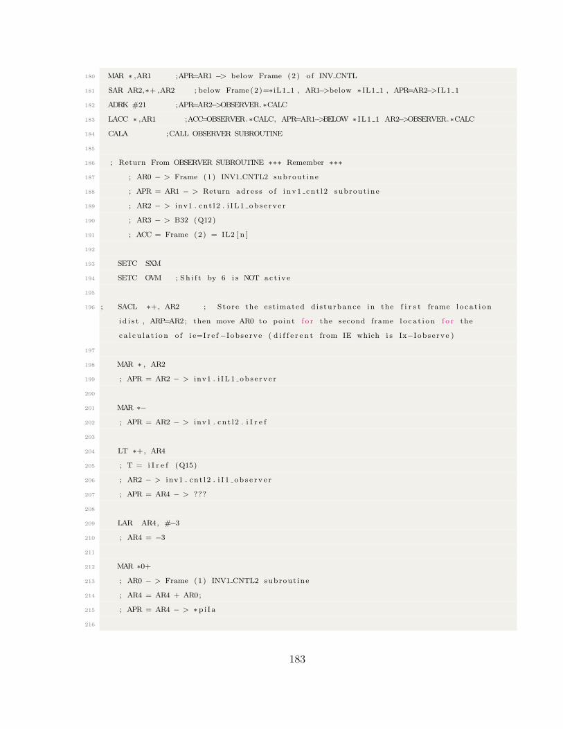
180 MAR ∗ ,AR1 ;APR=AR1 −> below Frame (2) o f INV CNTL
181 SAR AR2,∗+ ,AR2 ; below Frame (2)=∗iL1 1 , AR1−>below ∗ IL1 1 , APR=AR2−>IL1 1
182 ADRK #21 ;APR=AR2−>OBSERVER.∗CALC
183 LACC ∗ ,AR1 ;ACC=OBSERVER.∗CALC, APR=AR1−>BELOW ∗ IL1 1 AR2−>OBSERVER.∗CALC
184 CALA ;CALL OBSERVER SUBROUTINE
185
186 ; Return From OBSERVER SUBROUTINE ∗∗∗ Remember ∗∗∗
187 ; AR0 − > Frame (1) INV1 CNTL2 subrout ine
188 ; APR = AR1 − > Return adre s s o f i n v 1 cn t l 2 subrout ine
189 ; AR2 − > inv1 . cn t l 2 . i I L1 ob s e r v e r
190 ; AR3 − > B32 (Q12)
191 ; ACC = Frame (2) = IL2 [ n ]
192
193 SETC SXM
194 SETC OVM ; Sh i f t by 6 i s NOT ac t i v e
195
196 ; SACL ∗+, AR2 ; Store the est imated d i s turbance in the f i r s t frame l o c a t i o n
i d i s t , ARP=AR2; then move AR0 to po int f o r the second frame l o c a t i o n f o r the
c a l c u l a t i o n o f i e=I r e f−I obse rve ( d i f f e r e n t from IE which i s Ix−I obse rve )
197
198 MAR ∗ , AR2
199 ; APR = AR2 − > inv1 . i I L1 ob s e r v e r
200
201 MAR ∗−
202 ; APR = AR2 − > inv1 . cn t l 2 . i I r e f
203
204 LT ∗+, AR4
205 ; T = i I r e f (Q15)
206 ; AR2 − > inv1 . cn t l 2 . i I 1 o b s e r v e r
207 ; APR = AR4 − > ???
208
209 LAR AR4, #−3
210 ; AR4 = −3
211
212 MAR ∗0+
213 ; AR0 − > Frame (1) INV1 CNTL2 subrout ine
214 ; AR4 = AR4 + AR0;
215 ; APR = AR4 − > ∗ p i I a
216
183

217 LAR AR4,∗
218 ; APR = AR4 = ∗(AR4) = (∗ p i I a )
219 ; AR4 −> p i I a
220
221 ADRK #6
222 ; APR = AR4 −> iC1 (Q12)
223
224 MPY ∗+,AR3
225 ; P = i I r e f ∗ iC1 (Q27)
226 ; AR4 − > iC2
227 ; AR2 − > i I 1 o b s e r v e r
228 ; APR = AR3 − > B32
229
230 PAC
231 ; ACC = i I r e f ∗ iC1 (Q27)
232
233 SBRK #15
234 ; APR = AR3 − > Vg 1 (Q15)
235
236 LT ∗−,AR4
237 ; T = Vg 1 (Q15)
238 ; AR3 − > Vo 1 (Q15)
239 ; APR = AR4 − > iC2 (Q12)
240
241 MPY ∗+
242 ; P = Vg 1∗ iC2 (Q27)
243 ; APR = AR4 − > iC3
244 ; AR2 − > i I 1 o b s e r v e r
245 ; AR3 − > Vo 1 (Q15)
246
247 MAR ∗+, AR2
248 ; APR = AR4 − > iC4
249 ; AR2 − > i I 1 o b s e r v e r (Q15)
250
251 LT ∗+, AR4
252 ; T = i I 1 o b s e r v e r (Q15)
253 ; AR2 − > i I 2 o b s e r v e r (Q15)
254 ; APR = AR4 − > iC4
255
184
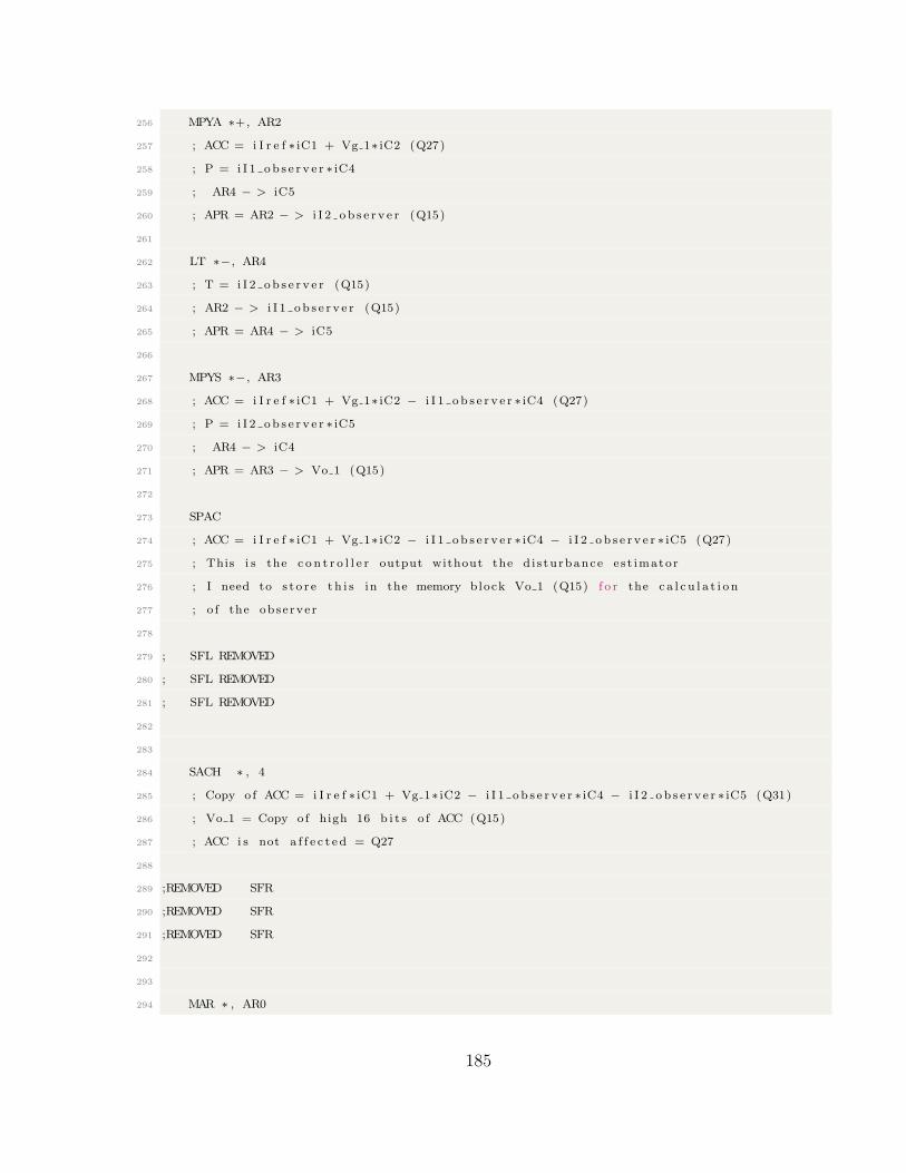
256 MPYA ∗+, AR2
257 ; ACC = i I r e f ∗ iC1 + Vg 1∗ iC2 (Q27)
258 ; P = i I 1 o b s e r v e r ∗ iC4
259 ; AR4 − > iC5
260 ; APR = AR2 − > i I 2 o b s e r v e r (Q15)
261
262 LT ∗−, AR4
263 ; T = i I 2 o b s e r v e r (Q15)
264 ; AR2 − > i I 1 o b s e r v e r (Q15)
265 ; APR = AR4 − > iC5
266
267 MPYS ∗−, AR3
268 ; ACC = i I r e f ∗ iC1 + Vg 1∗ iC2 − i I 1 o b s e r v e r ∗ iC4 (Q27)
269 ; P = i I 2 o b s e r v e r ∗ iC5
270 ; AR4 − > iC4
271 ; APR = AR3 − > Vo 1 (Q15)
272
273 SPAC
274 ; ACC = i I r e f ∗ iC1 + Vg 1∗ iC2 − i I 1 o b s e r v e r ∗ iC4 − i I 2 o b s e r v e r ∗ iC5 (Q27)
275 ; This i s the c o n t r o l l e r output without the d i s turbance e s t imator
276 ; I need to s t o r e t h i s in the memory block Vo 1 (Q15) f o r the c a l c u l a t i o n
277 ; o f the obse rve r
278
279 ; SFL REMOVED
280 ; SFL REMOVED
281 ; SFL REMOVED
282
283
284 SACH ∗ , 4
285 ; Copy o f ACC = i I r e f ∗ iC1 + Vg 1∗ iC2 − i I 1 o b s e r v e r ∗ iC4 − i I 2 o b s e r v e r ∗ iC5 (Q31)
286 ; Vo 1 = Copy o f high 16 b i t s o f ACC (Q15)
287 ; ACC i s not a f f e c t e d = Q27
288
289 ;REMOVED SFR
290 ;REMOVED SFR
291 ;REMOVED SFR
292
293
294 MAR ∗ , AR0
185

295 ; APR = AR0 − > Frame (1) INV1 CNTL2 −> i d i s t (Q14)
296 ; AR4 − > iC4 (Q12)
297
298 LT ∗+, AR4
299 ; T = i d i s t (Q14)
300 ; AR0 − > Frame (2) INV1 CNTL2
301 ; APR = AR4 − > iC4 (Q12)
302
303 MAR ∗−
304 ; APR = AR4 − > iC3 (Q13)
305
306 MPY ∗+, AR0
307 ; P = i d i s t ∗ iC3 (Q27)
308 ; APR = AR0 − > Frame (2) INV1 CNTL2
309 ; AR4 − > iC4 (Q12)
310
311 SPAC
312 ; ACC = i I r e f ∗ iC1 + Vg 1∗ iC2 − i I 1 o b s e r v e r ∗ iC4 − i I 2 o b s e r v e r ∗ iC5 − i d i s t ∗ iC3 (Q27)
313 ; ACC = Cont r o l l e r output be f o r e d i v i d i ng by Vdc
314
315
316
317
318
319 ; ∗∗∗∗∗∗∗∗∗∗∗∗∗∗∗∗∗∗∗∗∗∗∗∗∗∗∗∗∗∗∗∗∗∗∗∗∗∗∗∗∗∗∗∗∗∗∗∗∗∗∗∗∗∗∗∗∗∗∗∗∗∗∗∗∗∗∗∗∗∗∗∗∗∗∗∗∗
320 ; ADRK #3 ; ARP=AR2, AR2−> i I r e f Q(15)
321 ; LACC ∗+ ; ACC = i I r e f , ARP=AR2−> i I o b s e r v e r (Q15)
322 ; SUB ∗+, AR0 ; ARP = AR0, ACC=i I r e f −i I o b s e r v e r (Q15) , AR2−>iC1 , AR0−>i e
323 ; SFR ; To change ACC from Q15 to Q14
324 ; SACL ∗ ; ARP = AR0, i e=i I r e f −i I ob s e r v e r , AR2−>iC1 , AR3−>
325
326 ; LT ∗−, AR2 ; T = i e (Q15) , ARP=AR2−>iC1 (Q10) , AR0−> i d i s t
327
328 ; MPY ∗+ ; AR2−>iC2 , P=i e ∗ iC1 (Q25)
329 ; PAC ; ACC = dI∗C1 without s h i f t (Q25)
330 ; SFL
331 ; SFL ; ACC = dI∗C1 (Q27)
332 ; LT ∗+, AR3 ; T=iC2 (Q12) , AR2−>iC3 , ARP=AR3−>p i I a
333 ; MAR ∗+ ; AR3−>piVgr id
186
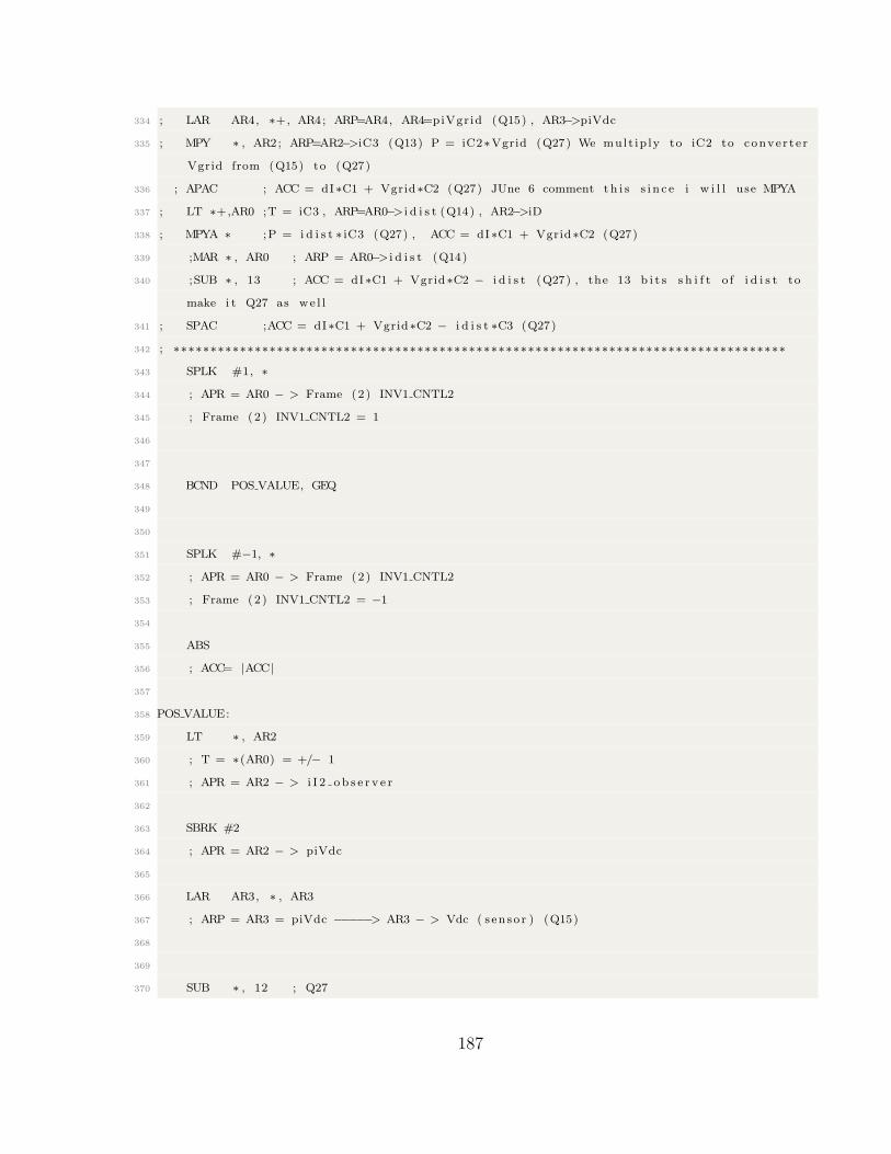
334 ; LAR AR4, ∗+, AR4; ARP=AR4, AR4=piVgrid (Q15) , AR3−>piVdc
335 ; MPY ∗ , AR2; ARP=AR2−>iC3 (Q13) P = iC2∗Vgrid (Q27) We mult ip ly to iC2 to conve r t e r
Vgrid from (Q15) to (Q27)
336 ; APAC ; ACC = dI∗C1 + Vgrid∗C2 (Q27) JUne 6 comment t h i s s i n c e i w i l l use MPYA
337 ; LT ∗+,AR0 ;T = iC3 , ARP=AR0−> i d i s t (Q14) , AR2−>iD
338 ; MPYA ∗ ;P = i d i s t ∗ iC3 (Q27) , ACC = dI∗C1 + Vgrid∗C2 (Q27)
339 ;MAR ∗ , AR0 ; ARP = AR0−> i d i s t (Q14)
340 ;SUB ∗ , 13 ; ACC = dI∗C1 + Vgrid∗C2 − i d i s t (Q27) , the 13 b i t s s h i f t o f i d i s t to
make i t Q27 as we l l
341 ; SPAC ;ACC = dI∗C1 + Vgrid∗C2 − i d i s t ∗C3 (Q27)
342 ; ∗∗∗∗∗∗∗∗∗∗∗∗∗∗∗∗∗∗∗∗∗∗∗∗∗∗∗∗∗∗∗∗∗∗∗∗∗∗∗∗∗∗∗∗∗∗∗∗∗∗∗∗∗∗∗∗∗∗∗∗∗∗∗∗∗∗∗∗∗∗∗∗∗∗∗∗∗∗∗∗∗∗∗
343 SPLK #1, ∗
344 ; APR = AR0 − > Frame (2) INV1 CNTL2
345 ; Frame (2) INV1 CNTL2 = 1
346
347
348 BCND POS VALUE, GEQ
349
350
351 SPLK #−1, ∗
352 ; APR = AR0 − > Frame (2) INV1 CNTL2
353 ; Frame (2) INV1 CNTL2 = −1
354
355 ABS
356 ; ACC= |ACC|
357
358 POS VALUE:
359 LT ∗ , AR2
360 ; T = ∗(AR0) = +/− 1
361 ; APR = AR2 − > i I 2 o b s e r v e r
362
363 SBRK #2
364 ; APR = AR2 − > piVdc
365
366 LAR AR3, ∗ , AR3
367 ; ARP = AR3 = piVdc −−−−−> AR3 − > Vdc ( s enso r ) (Q15)
368
369
370 SUB ∗ , 12 ; Q27
187

371 ; ACC = ACC − ∗(AR3)<<12
372 ; ACC = Cont r o l l e r output (Q27) − Vdc (Q(15+12)=Q27)
373 ; To check i f the c o n t r o l l e r output i s g r e a t e r than the phy s i c a l
374 ; va lue which i s Vdc
375
376
377 BCND POS NOT OV, LT
378 ; I f ACC = Cont r o l l e r output (Q27) − Vdc (Q(15+12)=Q27) < 0 , Then
379 ; the output o f the c o n t r o l l e r i s l e s s than Vdc
380
381
382 LACC #32767
383 ; E l se Load the ACC by the maximum po s s i b l e va lue f o r 16−b i t s igned value
384
385 MAR ∗ , AR0
386 ; APR = AR0 − > Frame (2) INV1 CNTL2 = +/− 1
387 B SIGN ADJ
388
389 POS NOT OV:
390 ADD ∗ , 12
391 ; To get the o r i g i n a l c o n t r o l l e r output
392 ; ACC = Cont r o l l e r output (Q27)
393
394 RPT #2
395 SFL
396 ; Repeat SFL twice so the t o t a l s h i f t s i s 3
397 ; ACC = Cont r o l l e r output (Q30)
398
399 RPT #15
400 SUBC ∗
401 ; Perform d i v i s i o n us ing c ond i t i o n a l sub t ra c t i on a lgor i thm
402 ; The d i v i s i o n i s :
403 ; Con t r o l l e r output (Q30) /Vdc ( s enso r ) (Q15)
404 ; = ACC = Reminder | r e s u l t s (Q15)
405 ; ∗∗∗∗∗∗ double check the r e s u l t o f d i v i s i on , in my note i t i s
406 ; Con t r o l l e r output (Q29) /Vdc ( s enso r ) (Q15)= Reminder | r e s u l t s (Q14)
407 ; however the SFL i s repeated 3 t imes so Con t r o l l e r output (Q30)
408 ; I ∗∗∗∗ I HAVE CHECKED −−> Result o f d i v i s i o n i s Q15
409
188

410
411 MAR ∗ , AR0
412 ; ACC High has the reminder o f the d i v i s i o n
413 ; ACC Low has the r e s u l t o f the d i v i s i o n
414 ; ACC = Reminder | ( Con t r o l l e r output ) /Vdc (Q15?)
415 ; APR = AR0 − > Frame (2) INV1 CNTL2 = +/− 1
416
417 SIGN ADJ :
418 SACL ∗
419 ; Frame (2) = ( Con t r o l l e r output ) /Vdc (Q15) which i s the | duty |
420 ; T = +/− 1 (Q1) the s i gn needed
421
422 MPY ∗ , AR4
423 ; P = T∗(∗AR0) = +/− 1 ∗ ( Con t r o l l e r output ) /Vdc (Q15)
424 ; T has the s ign , P=T∗duty
425 ; APR = AR4 − > iC4
426
427 ADRK #2
428 ; APR = AR4 − > iD
429
430 PAC
431 ;ACC = duty with s i gn adjusted , i . e . ACC=+/−1∗(Con t r o l l e r output ) /Vdc (Q15)
432
433 SACL ∗
434 ; ∗(AR4) = iD = ACC = duty (Q15)
435
436 BCND ZEROCOMP, EQ
437 BCND NEGCOMP, LT
438 ADD #DBCOMPENSATION
439 SACL ∗
440 SUB #32767
441 BCND ZEROCOMP, LEQ
442 SPLK #32767 , ∗
443 B ZEROCOMP
444 NEGCOMP:
445 SUB #DBCOMPENSATION
446 SACL ∗
447 SUB #−32767
448 BCND ZEROCOMP, GEQ
189

449 SPLK #−32767, ∗
450 B ZEROCOMP
451
452 ZEROCOMP:
453 LACC ∗+
454 ; ACC = iD = duty (Q15) a f t e r compensation
455 ; AR4 − > PWM. Period
456
457 CLRC OVM ; c l e a r over f l ow mode
458
459 ADRK #2
460 ; AR4 − > PWM. duty c1
461
462
463 SACL ∗
464 ; pwm. duty c1 = ACC = duty (Q15) a f t e r compensation
465
466 SBRK #2
467 ; AR4 − > PWM. Period
468
469 MAR ∗ , AR1
470 ; APR = AR1 − > Return adre s s o f i n v 1 cn t l 2 subrout ine
471
472 MAR ∗−
473 ; APR = AR1 − > below Frame (2) o f INV CNTL subrout ine
474
475 SAR AR4, ∗+, AR4
476 ; Below Frame (2) = ∗Period
477 ; AR1 − > below ∗Period
478 ; APR = AR4 − > PWM. Period
479
480 ADRK #4
481 ; APR = AR4 − > PWM.∗ update
482
483 LACC ∗ , AR0
484 ; ACC = PWM.∗ update
485 ; AR4 − > PWM.∗ update
486 ; AR1 = below ∗Period
487 ; APR = AR0 − > Frame (2) INV CNTL
190
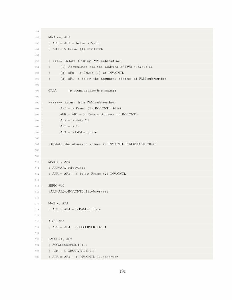
488
489 MAR ∗−, AR1
490 ; APR = AR1 = below ∗Period
491 ; AR0 − > Frame (1) INV CNTL
492
493 ; ∗∗∗∗∗ Before Ca l l i ng PWM subrout ine :
494 ; ( 1 ) Accumlator has the address o f PWM subrout ine
495 ; ( 2 ) AR0 − > Frame (1) o f INV CNTL
496 ; ( 3 ) AR1 −> below the argument address o f PWM subrout ine
497
498 CALA ; p−>pwm. update (&(p−>pwm) )
499
500 ; ∗∗∗∗∗∗∗ Return from PWM subrout ine :
501 ; AR0 − > Frame (1) INV CNTL i d i s t
502 ; APR = AR1 − > Return Address o f INV CNTL
503 ; AR2 − > duty C1
504 ; AR3 − > ??
505 ; AR4 − > PWM.∗ update
506
507 ; Update the obse rve r va lue s in INV CNTL REMOVED 20170428
508
509
510 ; MAR ∗−, AR2
511 ; ARP=AR2−>duty c1 ;
512 ; APR = AR1 − > below Frame (2) INV CNTL
513
514 ; SBRK #10
515 ;ARP=AR2−>INV CNTL. I 1 ob s e r v e r ;
516
517 ; MAR ∗ , AR4
518 ; APR = AR4 − > PWM.∗ update
519
520 ; ADRK #15
521 ; APR = AR4 − > OBSERVER. IL1 1
522
523 ; LACC ∗+, AR2
524 ; ACC=OBSERVER. IL1 1
525 ; AR4 − > OBSERVER. IL2 1
526 ; APR = AR2 − > INV CNTL. I 1 ob s e r v e r
191
527
528 ; SACL ∗+,AR4
529 ; INV CNTL. I 1 ob s e r v e r = OBSERVER. IL1 1
530 ; AR2 − > INV CNTL. I 2 ob s e r v e r
531 ; APR = AR4 − > OBSERVER. IL2 1
532
533
534 ; LACC ∗ , AR2
535 ; ACC=OBSERVER. IL2 1
536 ; AR4 − > OBSERVER. IL2 1
537 ; APR = AR2 − > INV CNTL. I 2 ob s e r v e r
538
539 ; SACL ∗ ,AR1
540 ; INV CNTL. I 2 ob s e r v e r = OBSERVER. IL2 1
541 ; AR2 − > INV CNTL. I 2 ob s e r v e r
542 ; APR = AR1 − > below Frame (2) INV CNTL
543
544
545 i nv1Cnt l2Update ex i t :
546
547 MAR ∗−,AR1 ; can be removed i f t h i s cond i t i on i s met on
548 ; every path to t h i s code .
549 ; s e t ARP = SP be f o r e you e x i t .
550 SBRK #( inv1Cnt l2Update f rames i z e+1)
551 ; d e a l l o c a t e frame , po int to saved FP
552 LAR AR0, ∗− ; r e s t o r e frame po in t e r
553 PSHD ∗ ; push re turn address on hardware s tack
554
555 RET
556
557 . end
Distrutance Estimator Assembly Code
1 ; /∗ ==============================================================================
2 ; System Name : S i ng l e phase i n v e r t e r
3
4 ; F i l e Name : d i s t e s t a . asm
5
192

6 ; De s c r ip t i on : implementation o f d i s tu rbance e s t imator .
7 ; Or i g ina to r : UNB
8
9 ; Target dependency : x2407
10 ;=====================================================================================
11 ; H i s tory :
12 ;−−−−−−−−−−−−−−−−−−−−−−−−−−−−−−−−−−−−−−−−−−−−−−−−−−−−−−−−−−−−−−−−−−−−−−−−−−−−−−−−−−−−−
13 ; 07−31−2008 Rev 1 .0 by Riming Shao
14 ;
15 ; 11−29−2008 Rev 2 .0 by Riming Shao
16 ; bug f ix : iE and iY need to be Q14
17 ;
18 ; 05−27−2016 Created by Haider Mohomad from d i g i t a l c o n t r o l l e r
================================================================================= ∗/
19
20 ;================================================================================
21 ; Routine Name : DIST EST Routine Type : C Ca l l ab l e
22 ;
23 ; De s c r ip t i on :
24 ;
25 ; C prototype : void d i s t E s t I n i t (DIGITAL CNTL1 ∗) ;
26 ; i n t16 d i s tEs tCa l c (DIGITAL CNTL1 ∗) ;
27 ; H i s tory c rea ted May 27 , 2016
28 ;================================================================================
29 ; D e f i n i t i o n o f DIST EST
30 ; /∗−−−−−−−−−−−−−−−−−−−−−−−−−−−−−−−−−−−−−−−−−−−−−−−−−−−−−−−−−−−−−−−−−−−−−−−−−−−−−−
31 ; Def ine the s t r u c tu r e o f the Object .
32 ;−−−−−−−−−−−−−−−−−−−−−−−−−−−−−−−−−−−−−−−−−−−−−−−−−−−−−−−−−−−−−−−−−−−−−−−−−−−−−−∗/
33 ;
34 ; /∗−−−−−−−−−−−−−−−−−−−−−−−−−−−−−−−−−−−−−−−−−−−−−−−−−−−−−−−−−−−−−−−−−−−−−−−−−−−−−−
35 ; Def ine the s t r u c tu r e o f the Object .
36 ;−−−−−−−−−−−−−−−−−−−−−−−−−−−−−−−−−−−−−−−−−−−−−−−−−−−−−−−−−−−−−−−−−−−−−−−−−−−−−−∗/
37 ;
38 ; typede f s t r u c t
39 ;
40 ; /∗−−−−−−−−−−−−−−−−−−−−−−−−−−−−−−−−−−−−−−−−−−−−−−−−−−−−−−−−−−−−−−−−−−−−−−−−−−−−−−
41 ; Dec l a ra t i on s f o r the ’ t e rmina l v a r i a b l e s ’ f o r the Algorithm . The framework
42 ; should communicate such quan t i t i e s as f r e q t e s t i n g , e t c to the a lgor i thm by
43 ; modifying these te rmina l v a r i a b l e s . I t i s not recommended that the framework
193

44 ; d i r e c t l y modify the i n t e r n a l v a r i b l e s o f the a lgor i thm .
45 ; −−−−−−−−−−−−−−−−−−−−−−−−−−−−−−−−−−−−−−−−−−−−−−−−−−−−−−−−−−−−−−−−−−−−−−−−−−−−−−∗/
46 ;
47 ; /∗−−−−−−−−−−−−−−−−−−−−−−−−−−−−−−−−−−−−−−−−−−−−−−−−−−−−−−−−−−−−−−−−−−−−−−−−−−−−−
48 ; (N0 + N1 ∗ zˆ−1 + N2 ∗ zˆ−2)
49 ; d i s t ( z ) = −−−−−−−−−−−−−−−−−−−−−−−−−−−− ∗ E( z ) ,E = X − Xref 1 f o r feedback system
50 ; (1 + D1 ∗ zˆ−1 + D2 ∗ zˆ−2)
51 ;−−−−−−−−−−−−−−−−−−−−−−−−−−−−−−−−−−−−−−−−−−−−−−−−−−−−−−−−−−−−−−−−−−−−−−−−−−−−−∗/
52 ;
53 ;
54 ; /∗−−−−−−−−−−−−−−−−−−−−−−−−−−−−−−−−−−−−−−−−−−−−−−−−−−−−−−−−−−−−−−−−−−−−−−−−−−−−−
55 ; Mi s ce l l aneous Items .
56 ;−−−−−−−−−−−−−−−−−−−−−−−−−−−−−−−−−−−−−−−−−−−−−−−−−−−−−−−−−−−−−−−−−−−−−−−−−−−−−∗/
57 ; i n t16 iXr e f ; // Q15 , input
58 ; i n t16 iXobserve ; // Q15 , input
59 ; i n t16 iX ; // Q15 , Input
60 ; i n t16 iE 1 ; // Q14 , v a r i ab l e ( Ix [ n−1] − iX r e f 1 [ n−1])
61 ; i n t16 iE 2 ; // Q14 , v a r i ab l e
62 ; i n t16 i d i s t 1 ; // Q14 , v a r i ab l e
63 ; i n t16 i d i s t 2 ; // Q14 , v a r i ab l e
64 ; i n t16 iN0 ; // Q14 , parameter
65 ; i n t16 iN1 ; // Q14 , parameter
66 ; i n t16 iN2 ; // Q14 , parameter
67 ; i n t16 iD1 ; // Q14 , parameter
68 ; i n t16 iD2 ; // Q14 , parameter
69 ;
70 ;
71 ; /∗−−−−−−−−−−−−−−−−−−−−−−−−−−−−−−−−−−−−−−−−−−−−−−−−−−−−−−−−−−−−−−−−−−−−−−−−−−−−−−
72 ; Dec la ra t i on f o r the f unc t i on s implemented in d i g i t a l c n t l 2 . c
73 ;−−−−−−−−−−−−−−−−−−−−−−−−−−−−−−−−−−−−−−−−−−−−−−−−−−−−−−−−−−−−−−−−−−−−−−−−−−−−−−∗/
74 ; void (∗ i n i t ) ( ) ; // po in t e r to a func t i on
75 ; i n t16 (∗ c a l c ) ( ) ;
76 ;
77 ; DIST EST ;
78
79
80
81 . i n c lude . . \ i n c lude \x240x . h
82
194

83
84 . de f d i s t E s t I n i t
85
86 d i s t E s t I n i t :
87
88 d i s t E s t I n i t f r am e s i z e . s e t 0
89
90
91 ;−−−−−−−−−−−−−−−−−−−−−−−−−−−−−−−−−−−−−−−−−−−−−−−−−−−−−−−−−−−−−−−−−−−−−−−−−−
92 ; ARP = AR1
93 ; AR1 i s s tack po in t e r (SP)
94 ; AR0 i s frame po in t e r (FP)
95 POPD ∗+ ; Save the re turn address from hardware
96 ; s tack onto the so f tware s tack
97 ; ARP = AR1
98
99 SAR AR0, ∗+ ; push AR0(FP) . ARP =AR1
100 SAR AR1, ∗ ; ∗SP = SP . ARP =AR1
101 LAR AR0, # d i s t E s t I n i t f r am e s i z e
102 ; FP = s i z e o f frame
103 LAR AR0, ∗0+, AR2 ; ARP = AR2.
104 ; A l l o ca t e frame . AR0 = ∗AR1
105 ; AR1 = AR1 + AR0.
106 ;−−−−−−−−−−−−−−−−−−−−−−−−−−−−−−−−−−−−−−−−−−−−−−−−−−−−−−−−−−−−−−−−−−−−−−−−−−
107 LAR AR2, #−3
108 MAR ∗0+ ; AR2 pts to f i r s t arguments , −− to next one
109 ; ARP = AR2, AR2 −> p
110 ;−−−−−−−−−−−−−−−−−−−−−−−−−−−−−−−−−−−−−−−−−−−−−−−−−−−−−−−−−−−−−−−−−−−−−−−−−−
111 LAR AR2,∗ ; AR2 po in t s to the f i r s t s t r u c tu r e member
112 ; ( i . e . AR2 −> iX r e f ) . ARP = AR2.
113 ; AR2 −> IL1 1 .
114 ;−−−−−−−−−−−−−−−−−−−−−−−−−−−−−−−−−−−−−−−−−−−−−−−−−−−−−−−−−−−−−−−−−−−−−−−−−−
115 ; ADRK #3 ; ARP = AR2, AR2−>IL1 1
116 LACL #0 ; Load ACC Low with constant 0 , i . e . ACCL=0x00
117 SACL ∗+ ; ARP = AR2, AR2−>IL1 2 , IL1 1 = ACCL
118 SACL ∗+ ; ARP = AR2, AR2−>Vc 1 , IL1 2 = ACCL
119 SACL ∗+ ; ARP = AR2, AR2−>V0 1 , Vc 1 = ACCL
120 SACL ∗+ ; ARP = AR2, AR2−>Vg 1 , V0 1 = ACCL
121 SACL ∗+, AR1 ; ARP = AR1, AR2−>A11 , Vg 1 = ACCL
195

122
123 d i s t E s t I n i t e x i t :
124
125 ; MAR ∗ ,AR1 ; can be removed i f t h i s cond i t i on i s met on
126 ; every path to t h i s code .
127 ; s e t ARP = SP be f o r e you e x i t .
128 SBRK #( d i s t E s t I n i t f r am e s i z e +1)
129 ; d e a l l o c a t e frame , po int to saved FP
130 LAR AR0, ∗− ; r e s t o r e frame po in t e r
131 PSHD ∗ ; push re turn address on hardware s tack
132 RET
133
134
135 . de f d i s tE s tCa l c
136
137 d i s tEs tCa l c :
138
139 d i s tE s tCa l c f r ame s i z e . s e t 2
140
141
142 ;−−−−−−−−−−−−−−−−−−−−−−−−−−−−−−−−−−−−−−−−−−−−−−−−−−−−−−−−−−−−−−−−−−−−−−−−−−
143 ; ARP = AR1
144 ; AR1 i s s tack po in t e r (SP)
145 ; AR0 i s frame po in t e r (FP)
146 POPD ∗+ ; Save the re turn address from hardware
147 ; s tack onto the so f tware s tack
148 ; ARP = AR1
149
150 SAR AR0, ∗+ ; push AR0(FP) . ARP =AR1
151 SAR AR1, ∗ ; ∗SP = SP . ARP =AR1
152 LAR AR0, # d i s tE s tCa l c f r ame s i z e
153 ; FP = s i z e o f frame
154 LAR AR0, ∗0+, AR2 ; ARP = AR2.
155 ; A l l o ca t e frame . AR0 = ∗AR1
156 ; AR1 = AR1 + AR0.
157 ;−−−−−−−−−−−−−−−−−−−−−−−−−−−−−−−−−−−−−−−−−−−−−−−−−−−−−−−−−−−−−−−−−−−−−−−−−−
158 LAR AR2, #−3
159 MAR ∗0+ ; AR2 pts to f i r s t arguments , −− to next one
160 ; ARP = AR2, AR2 −> p
196

161 ;−−−−−−−−−−−−−−−−−−−−−−−−−−−−−−−−−−−−−−−−−−−−−−−−−−−−−−−−−−−−−−−−−−−−−−−−−−
162 LAR AR3,∗ ; AR3 po in t s to the f i r s t s t r u c tu r e member
163 ; ( i . e . AR3 −> iX r e f ) . ARP = AR2.
164 ;−−−−−−−−−−−−−−−−−−−−−−−−−−−−−−−−−−−−−−−−−−−−−−−−−−−−−−−−−−−−−−−−−−−−−−−−−−
165 LAR AR2,∗ ; AR2 po in t s to the f i r s t s t r u c tu r e member
166 ; ( i . e . AR2 −> iX r e f ) . ARP = AR2.
167 ; AR2 −> iX r e f .
168 ;−−−−−−−−−−−−−−−−−−−−−−−−−−−−−−−−−−−−−−−−−−−−−−−−−−−−−−−−−−−−−−−−−−−−−−−−−−
169
170 SETC SXM
171 SETC OVM
172 SPM 3 ; SFR 6 BITS
173
174 ADRK #2 ; ARP=AR2−>iX
175 ;MAR ∗+, AR2 ; ARP = AR2; AR2−>iXobserve
176 ;MAR ∗+ ; ARP = AR2; AR2−>iX
177 LACC ∗− ; ARP = AR2, ACC=iX , AR2−>iXobsever
178 SUB ∗+, AR0 ; ARP = AR0, ACC=iX−iXobserve , AR2−>iX , AR0−>iE (Frame 1)
179 SFR ; To change iE from Q15 to Q14
180 SACL ∗ ; ARP = AR0, Store the updated iE in Frame (1) , iE=iX−iXobserve , AR2−>
iX , AR3−>iX r e f
181 LT ∗+, AR3 ; ARP = AR3, T=iE (Q14) , AR2−>iX , AR3−>iXre f , AR0−> i d i s t (Frame 2)
182 ADRK #7 ; ARP = AR3, AR2−>iX , AR3−>iN0 , AR0−> i d i s t
183 MPY ∗+, AR2 ; ARP = AR2, AR2−>iX , AR3−>iN1 , P=T∗(∗AR3) i . e . P=iE∗ iN0 (Q28)
184 PAC ; ACC = ( iN0∗ iE )>>6, Q22
185 MAR ∗+ ; AR2−>iE 1
186 LT ∗+, AR3 ; ARP = AR3, T=iE 1 (Q14) , AR2−>iE 2 , AR3−>iN1 , AR0−> i d i s t
187
188 MPY ∗+, AR2 ; ARP = AR2, AR2−>iE 2 , AR3−>iN2 , P = ( iN1∗ iE 1 ) (Q28)
189 LT ∗+, AR3 ; ARP = AR3, T=iE 2 (Q14) , AR2−>i d i s t 1 , AR3−>iN2 ,AR0−> i d i s t
190
191 MPYA ∗+, AR2 ; ARP = AR2, AR2−>i d i s t 1 , AR3−>iD1 , P = ( iN2∗ iE 2 ) (Q28) , ACC = (
iN0∗ iE+iN1∗ iE 1 )>>6 (Q22)
192 LT ∗+, AR3 ; ARP = AR3, T=i d i s t 1 (Q14) , AR2−>i d i s t 2 , AR3−>iD1
193
194 MPYA ∗+, AR2 ; ARP = AR2, AR2−>i d i s t 2 , AR3−>iD2 , P = ( iD1∗ i d i s t 1 ) (Q28)
195 ; ACC = ( iN0∗ iE+iN1∗ iE 1+iN2∗ iE 2 )>>6 (Q22)
196 LT ∗+, AR3 ; ARP = AR3, T=i d i s t 2 (Q14) , AR2−>iN 0 , AR3−>iD2
197

197 MPYS ∗+, AR0 ; ARP = AR0, AR2−>iN 0 , AR3−>i n i t , P = ( iD2∗ i d i s t 2 ) (Q28) ,AR0−>
i d i s t
198 ; ACC = ( iN0∗ iE+iN1∗ iE 1+iN2∗ iE 2−iD1∗ i d i s t 1 )>>6, Q22
199 ; AR0−>iY
200 SPAC ; ACC = RESULT = ( iN0∗ iE+iN1∗ iE 1+iN2∗ iE 2−iD1∗ iY 1−iD2∗ i d i s t 2 )>>6 (
Q22)
201
202 ; ; ; ; ; ; This s h i f t i s to mult ip ly i d i s t by the gain , modify here
203 ; ; RPT #3
204 ; ; SFL ; ACC i s s t i l l Q22 s i n c e t h i s s h i f t i s mu l t i p l i c a t i o n
205
206 SUB #1<<8, 15 ; SATUATION PROTECTION
207 BCND OVPROTEC, GEQ
208
209 ADD #1<<9, 15 ; ORIGINAL − (−1ˆ24)
210 BCND UV PROTEC, LT
211
212 SUB #1<<8, 15
213 SFL ; RESULT (Q23)
214 SACH ∗ , 7 ; S h i f t the ACC by 7 b i t s wish w i l l make RESULT in the ACC (Q30) ,
Then s t o r e the ACCH (16 MSB) in the addressed memory l o c a t i o n : AR0−> i d i s t = RESULT.
This w i l l s t o r e (B16−31) which w i l l make i d i s t (Q14)
215
216 B ENDPROTEC
217
218 OVPROTEC:
219 SPLK #32767 , ∗ ; AR0−> i d i s t = RESULT
220 B ENDPROTEC
221
222 UVPROTEC:
223 SPLK #−32768, ∗ ; AR0−> i d i s t = RESULT
224
225 ENDPROTEC:
226
227 MAR ∗−, AR2 ;ARP = AR2, AR2−>iN 0
228
229 SBRK #4 ; ARP = AR2, AR2−>iE 1
230 LACC ∗+ ; ARP = AR2, AR2−>iE 2 , ACC = iE 1
231 SACL ∗−, AR0 ; ARP = AR2, AR2−>iE 1 , iE 2 = iE 1 , AR0−> i d i s t
198

232 ;MAR ∗− ; AR0−>iE
233 LACC ∗+, AR2 ; ARP = AR2, AR2−>iE 1 , ACC = iE , AR0−> i d i s t
234 SACL ∗+ ; ARP = AR2, AR2−>iE 2 , iE 1 = iE , AR0−> i d i s t
235 MAR ∗+ ; ARP = AR2, AR2−> i d i s t 1
236 LACC ∗+ ; ARP = AR2, AR2−>i d i s t 2 , ACC = i d i s t 1
237 SACL ∗−, AR0 ; ARP = AR0, AR2−>i d i s t 1 , i d i s t 2 = i d i s t 1
238 LACC ∗ , AR2 ; ARP = AR2, AR2−>i d i s t 1 , ACC = i d i s t
239 SACL ∗ ,AR1 ; ARP = AR1, AR2−>i d i s t 1 , i d i s t 1 = i d i s t , AR0−> i d i s t
240
241
242
243 d i s tE s tC a l c e x i t :
244
245 CLRC OVM
246 SPM 0
247
248 ; MAR ∗ ,AR1 ; can be removed i f t h i s cond i t i on i s met on
249 ; every path to t h i s code .
250 ; s e t ARP = SP be f o r e you e x i t .
251 SBRK #( d i s tE s tCa l c f r ame s i z e +1)
252 ; d e a l l o c a t e frame , po int to saved FP
253 LAR AR0, ∗− ; r e s t o r e frame po in t e r
254 PSHD ∗ ; push re turn address on hardware s tack
255
256 RET
257
258 . end
Observer Assembly Code
1 ; /∗ ==============================================================================
2 ; System Name : S i ng l e phase i n v e r t e r
3
4 ; F i l e Name : obse rve r . asm
5
6 ; De s c r ip t i on : implementation o f I nv e r t e r with LCL F i l t e r Observer .
7 ; Or i g ina to r : UNB
8
9 ; Target dependency : x2407
199

10 ;=====================================================================================
11 ; H i s tory :
12 ;−−−−−−−−−−−−−−−−−−−−−−−−−−−−−−−−−−−−−−−−−−−−−−−−−−−−−−−−−−−−−−−−−−−−−−−−−−−−−−−−−−−−−
13 ;
14 ; 04−12−2017 Created by Haider Mohomad A Razak
================================================================================= ∗/
15
16 ;================================================================================
17 ; Routine Name : obse rve r Routine Type : C Ca l l ab l e
18 ;
19 ; De s c r ip t i on :
20 ;
21 ; C prototype : void ob s e r v e r I n i t (DIGITAL CNTL1 ∗) ;
22 ; i n t16 observerCa lc (DIGITAL CNTL1 ∗) ;
23 ; H i s tory c rea ted Apr i l 19 , 2017
24 ;================================================================================
25 ; D e f i n i t i o n o f OBSERVER
26 ; /∗−−−−−−−−−−−−−−−−−−−−−−−−−−−−−−−−−−−−−−−−−−−−−−−−−−−−−−−−−−−−−−−−−−−−−−−−−−−−−−
27 ; Def ine the s t r u c tu r e o f the Object .
28 ;−−−−−−−−−−−−−−−−−−−−−−−−−−−−−−−−−−−−−−−−−−−−−−−−−−−−−−−−−−−−−−−−−−−−−−−−−−−−−−∗/
29 ;
30 ; /∗−−−−−−−−−−−−−−−−−−−−−−−−−−−−−−−−−−−−−−−−−−−−−−−−−−−−−−−−−−−−−−−−−−−−−−−−−−−−−−
31 ; Def ine the s t r u c tu r e o f the Object .
32 ;−−−−−−−−−−−−−−−−−−−−−−−−−−−−−−−−−−−−−−−−−−−−−−−−−−−−−−−−−−−−−−−−−−−−−−−−−−−−−−∗/
33 ;
34 ; typede f s t r u c t
35 ;
36 ; /∗−−−−−−−−−−−−−−−−−−−−−−−−−−−−−−−−−−−−−−−−−−−−−−−−−−−−−−−−−−−−−−−−−−−−−−−−−−−−−−
37 ; Dec l a ra t i on s f o r the ’ t e rmina l v a r i a b l e s ’ f o r the Algorithm . The framework
38 ; should communicate such quan t i t i e s as f r e q t e s t i n g , e t c to the a lgor i thm by
39 ; modifying these te rmina l v a r i a b l e s . I t i s not recommended that the framework
40 ; d i r e c t l y modify the i n t e r n a l v a r i b l e s o f the a lgor i thm .
41 ; −−−−−−−−−−−−−−−−−−−−−−−−−−−−−−−−−−−−−−−−−−−−−−−−−−−−−−−−−−−−−−−−−−−−−−−−−−−−−−∗/
42 ;
43 ; /∗−−−−−−−−−−−−−−−−−−−−−−−−−−−−−−−−−−−−−−−−−−−−−−−−−−−−−−−−−−−−−−−−−−−−−−−−−−−−−
44 ;
45 ; X[ n+1]=A X[ n]+B U[ n ]
46 ;
47 ; X=[ IL1 IL2 VC]
200

48 ; U=[VO VG]
49 ;
50 ;−−−−−−−−−−−−−−−−−−−−−−−−−−−−−−−−−−−−−−−−−−−−−−−−−−−−−−−−−−−−−−−−−−−−−−−−−−−−−∗/
51 ;
52 ;
53 ; /∗−−−−−−−−−−−−−−−−−−−−−−−−−−−−−−−−−−−−−−−−−−−−−−−−−−−−−−−−−−−−−−−−−−−−−−−−−−−−−
54 ; Mi s ce l l aneous Items .
55 ;−−−−−−−−−−−−−−−−−−−−−−−−−−−−−−−−−−−−−−−−−−−−−−−−−−−−−−−−−−−−−−−−−−−−−−−−−−−−−∗/
56 ; i n t16 iL1 1 ; // Q15 , input IL1 [ n−1]
57 ; i n t16 iL2 1 ; // Q15 , input IL2 [ n−1]
58 ; i n t16 Vc 1 ; // Q15 , input Vc [ n−1]
59 ; i n t16 Vo 1 ; // Q15 , input Vo [ n−1]
60 ; i n t16 Vg 1 ; // Q15 , input Vg [ n−1]
61 ; i n t16 A11 ; // Q12 , A11 =??? a11∗IMAX/VDCMAX∗2ˆ12
62 ; i n t16 A12 ; // Q12 , A12 =??? a12∗VGRIDMAX/VDCMAX∗2ˆ12
63 ; i n t16 A13 ; // Q12 , A12 =??? a12∗VGRIDMAX/VDCMAX∗2ˆ12
64 ; i n t16 B11 ; // Q12 , A12 =??? a12∗VGRIDMAX/VDCMAX∗2ˆ12
65 ; i n t16 B12 ; // Q12 , A12 =??? a12∗VGRIDMAX/VDCMAX∗2ˆ12
66 ; i n t16 A21 ; // Q12 , A11 =??? a11∗IMAX/VDCMAX∗2ˆ12
67 ; i n t16 A22 ; // Q12 , A12 =??? a12∗VGRIDMAX/VDCMAX∗2ˆ12
68 ; i n t16 A23 ; // Q12 , A12 =??? a12∗VGRIDMAX/VDCMAX∗2ˆ12
69 ; i n t16 B21 ; // Q12 , A12 =??? a12∗VGRIDMAX/VDCMAX∗2ˆ12
70 ; i n t16 B22 ; // Q12 , A12 =??? a12∗VGRIDMAX/VDCMAX∗2ˆ12
71 ; i n t16 A31 ; // Q12 , A11 =??? a11∗IMAX/VDCMAX∗2ˆ12
72 ; i n t16 A32 ; // Q12 , A12 =??? a12∗VGRIDMAX/VDCMAX∗2ˆ12
73 ; i n t16 A33 ; // Q12 , A12 =??? a12∗VGRIDMAX/VDCMAX∗2ˆ12
74 ; i n t16 B31 ; // Q12 , A12 =??? a12∗VGRIDMAX/VDCMAX∗2ˆ12
75 ; i n t16 B32 ; // Q12 , A12 =??? a12∗VGRIDMAX/VDCMAX∗2ˆ1
76
77 ;
78 ;
79 ; /∗−−−−−−−−−−−−−−−−−−−−−−−−−−−−−−−−−−−−−−−−−−−−−−−−−−−−−−−−−−−−−−−−−−−−−−−−−−−−−−
80 ; Dec la ra t i on f o r the f unc t i on s implemented in d i g i t a l c n t l 2 . c
81 ;−−−−−−−−−−−−−−−−−−−−−−−−−−−−−−−−−−−−−−−−−−−−−−−−−−−−−−−−−−−−−−−−−−−−−−−−−−−−−−∗/
82 ; void (∗ i n i t ) ( ) ; // po in t e r to a func t i on
83 ; i n t16 (∗ c a l c ) ( ) ;
84 ;
85 ; OBSERVER;
86
201
87
88
89 . i n c lude . . \ i n c lude \x240x . h
90
91
92 . de f o b s e r v e r I n i t
93
94 ob s e r v e r I n i t :
95
96 o b s e r v e r I n i t f r am e s i z e . s e t 3
97
98
99 ;−−−−−−−−−−−−−−−−−−−−−−−−−−−−−−−−−−−−−−−−−−−−−−−−−−−−−−−−−−−−−−−−−−−−−−−−−−
100 ; ARP = AR1
101 ; AR1 i s s tack po in t e r (SP)
102 ; AR0 i s frame po in t e r (FP)
103 POPD ∗+ ; Save the re turn address from hardware
104 ; s tack onto the so f tware s tack
105 ; ARP = AR1
106
107 SAR AR0, ∗+ ; push AR0(FP) . ARP =AR1
108 SAR AR1, ∗ ; ∗SP = SP . ARP =AR1
109 LAR AR0, # ob s e r v e r I n i t f r am e s i z e
110 ; FP = s i z e o f frame
111 LAR AR0, ∗0+, AR2 ; ARP = AR2.
112 ; A l l o ca t e frame . AR0 = ∗AR1
113 ; AR1 = AR1 + AR0.
114 ;−−−−−−−−−−−−−−−−−−−−−−−−−−−−−−−−−−−−−−−−−−−−−−−−−−−−−−−−−−−−−−−−−−−−−−−−−−
115 LAR AR2, #−3
116 MAR ∗0+ ; AR2 pts to f i r s t arguments , −− to next one
117 ; ARP = AR2, AR2 −> p
118 ; b e f o r e we s t a r t the c a l c u l a t i o n o f the observer , we need to arrange
119 ; the so f tware s tack such that :
120 ; 1) The re turn address o f the o r i g i n a l subrout ine (INV CNT)
121 ; 2) The frame address o f the o r i g i n a l subrout ine (INV CNT)
122 ; 3) Locate new frame o f the c a l l e d subrout ine ( Observer )
123 ; 4) AR2 − > address o f the f i r s t argument o f the c a l l e d subrout ine ( Observer )
124 ; 5) AR0 −> f i r s t frame o f the c a l l e d subrout ine ( Observer )
202
125 ; 6) AR1 −> empty space below the l a s t frame o f the c a l l e d subrout ine ( Observer
)
126 ;−−−−−−−−−−−−−−−−−−−−−−−−−−−−−−−−−−−−−−−−−−−−−−−−−−−−−−−−−−−−−−−−−−−−−−−−−−
127 LAR AR2,∗ ; AR2 po in t s to the f i r s t s t r u c tu r e member
128 ; ( i . e . AR2 −> i IL1 1 ) . ARP = AR2.
129 ; AR2 −> i IL1 1 .
130 ;−−−−−−−−−−−−−−−−−−−−−−−−−−−−−−−−−−−−−−−−−−−−−−−−−−−−−−−−−−−−−−−−−−−−−−−−−−
131 ; ADRK #3 ; ARP = AR2, AR2−>iE 1
132 LACL #0 ; Load ACC Low with constant 0 , i . e . ACCL=0x00
133 SACL ∗+ ; ARP = AR2, AR2−>VC 1 , i IL1 1 = ACCL = 0
134 SACL ∗+ ; ARP = AR2, AR2−>i IL2 1 , i IL2 1 = ACCL = 0
135 ; SACL ∗+ ; ARP = AR2, AR2−>Vo 1 , VC 1 = ACCL = 0
136 ; SACL ∗+ ; ARP = AR1, AR2−>Vg 1 , V0 1 = ACCL = 0
137 SACL ∗+, AR1 ; ARP = AR1, AR2−>A11 , VC 1 = ACCL = 0
138
139 o b s e r v e r I n i t e x i t :
140
141 ; MAR ∗ ,AR1 ; can be removed i f t h i s cond i t i on i s met on
142 ; every path to t h i s code .
143 ; s e t ARP = SP be f o r e you e x i t .
144 SBRK #( ob s e r v e r I n i t f r am e s i z e +1)
145 ; d e a l l o c a t e frame , po int to saved FP
146 LAR AR0, ∗− ; r e s t o r e frame po in t e r
147 PSHD ∗ ; push re turn address on hardware s tack
148 RET
149
150
151 . de f obse rve rCa l c
152
153 obse rve rCa l c :
154
155 ob s e r v e rCa l c f r ame s i z e . s e t 3
156
157
158 ;−−−−−−−−−−−−−−−−−−−−−−−−−−−−−−−−−−−−−−−−−−−−−−−−−−−−−−−−−−−−−−−−−−−−−−−−−−
159 ; ARP = AR1
160 ; AR1 i s s tack po in t e r (SP)
161 ; AR0 i s frame po in t e r (FP)
162 POPD ∗+ ; Save the re turn address from hardware
203
163 ; s tack onto the so f tware s tack
164 ; ARP = AR1
165
166 SAR AR0, ∗+ ; push AR0(FP) . ARP =AR1
167 ; AR0 − > Frame (1) INV CNTL
168 ; APR = AR1 − > below INV CNTL Frame Address
169 SAR AR1, ∗ ; ∗SP = SP . ARP =AR1
170 LAR AR0, # ob s e r v e rCa l c f r ame s i z e
171 ; FP = s i z e o f frame
172 LAR AR0, ∗0+, AR2 ; ARP = AR2.
173 ; A l l o ca t e frame . AR0 = ∗AR1
174 ; AR1 = AR1 + AR0.
175 ;−−−−−−−−−−−−−−−−−−−−−−−−−−−−−−−−−−−−−−−−−−−−−−−−−−−−−−−−−−−−−−−−−−−−−−−−−−
176 LAR AR2, #−3
177 MAR ∗0+ ; AR2 pts to f i r s t arguments , −− to next one
178 ; ARP = AR2, AR2 −> p
179
180 ; b e f o r e we s t a r t the c a l c u l a t i o n o f the observer , we need to arrange
181 ; the so f tware s tack such that :
182 ; 1) The re turn address o f the o r i g i n a l subrout ine (INV CNT)
183 ; 2) The frame address o f the o r i g i n a l subrout ine (INV CNT)
184 ; 3) Locate new frame o f the c a l l e d subrout ine ( Observer )
185 ; 4) AR2 − > address o f the f i r s t argument o f the c a l l e d subrout ine ( Observer )
186 ; 5) AR0 −> f i r s t frame o f the c a l l e d subrout ine ( Observer )
187 ; 6) AR1 −> empty space below the l a s t frame o f the c a l l e d subrout ine ( Observer
)
188 ;−−−−−−−−−−−−−−−−−−−−−−−−−−−−−−−−−−−−−−−−−−−−−−−−−−−−−−−−−−−−−−−−−−−−−−−−−−
189
190 LAR AR3,∗ ; AR3 po in t s to the f i r s t s t r u c tu r e member
191 ; ( i . e . AR3 −> i IL1 1 ) . ARP = AR2.
192
193 ; LAR AR4,∗ ; AR4 po in t s to the f i r s t s t r u c tu r e member
194 ; ( i . e . AR4 −> i IL1 1 ) . ARP = AR2.
195 ;−−−−−−−−−−−−−−−−−−−−−−−−−−−−−−−−−−−−−−−−−−−−−−−−−−−−−−−−−−−−−−−−−−−−−−−−−−
196 ; LAR AR2,∗ ; AR2 po in t s to the f i r s t s t r u c tu r e member
197 ; ( i . e . AR2 −> i IL1 1 ) . ARP = AR2.
198 ; AR2 −> i IL1 1 .
199 LAR AR4,∗ ; AR4 −> i IL1 1
200 ;−−−−−−−−−−−−−−−−−−−−−−−−−−−−−−−−−−−−−−−−−−−−−−−−−−−−−−−−−−−−−−−−−−−−−−−−−−
204

201 LAR AR2,∗ ,AR2 ; AR2 po in t s to the f i r s t s t r u c tu r e member
202 ; ( i . e . AR2 −> p i I a ) . ARP = AR4 −> i IL1 1 .
203 ; AR2 −> i IL1 1 .
204
205 ; ROMOVED ON 20170428 , I need to use the vg [ n−1] f o r c a l c u l a t i o n t h e r e f o r e I
206 ; need to update vg a f t e r c a l c u l a t i n g
207
208 ; SBRK #30 ; ARP = AR4 −> piVgr id
209 ; LAR AR4,∗ ; AR4 = ∗(AR4) = ∗( piVgr id ) = Vgrid
210 ; LACC ∗ ,AR3 ; ACC=Vgrid , AR3 −> i IL1 1
211 ; ADRK #4 ; APR=AR3 − > Observer .Vg
212 ; SACL ∗+,AR2 ; Observer .Vg = Vgrid
213 ; AR3 − > A11
214 ; APR=AR2 − > i IL1 1
215
216
217
218
219 ;−−−−−−−−−−−−−−−−−−−−−−−−−−−−−−−−−−−−−−−−−−−−−−−−−−−−−−−−−−−−−−−−−−−−−−−−−−
220
221 SETC SXM
222 SETC OVM
223 SPM 3 ; SFR 6 BITS
224
225 LT ∗+, AR3 ; T=i IL1 1 (Q15) , AR2−>i IL1 2 , APR=AR3−>i IL1 1 , AR0−>(Frame 1)
226 ADRK #5 ; ARP = AR3−>A11
227 MPY ∗+, AR2 ; P=T∗(∗AR3) i . e . P=i IL1 1 ∗A11 (Q27)
228 ; AR3 −> A12
229 ; APR = AR2 −> iL2 1
230 PAC ; ACC = ( i IL1 1 ∗A11)>>6, (Q21)
231 ;MAR ∗+ ; AR2−>iL2 1
232 LT ∗+, AR3 ; T=iL2 1 (Q15) , AR2−>VC 1 , APR=AR3−>A12(Q12) , AR0−>(Frame 1)
233
234 MPY ∗+, AR2 ; ARP = AR2 − > VC 1 (Q15) , AR3−>A13(Q12) , P = ( iL2 1 ∗A12) (Q27)
235 LT ∗+, AR3 ; ARP = AR3 − > A13 (Q12) , T=VC 1 (Q15) , AR2−>Vo 1 (Q15)
236
237
238
239
205
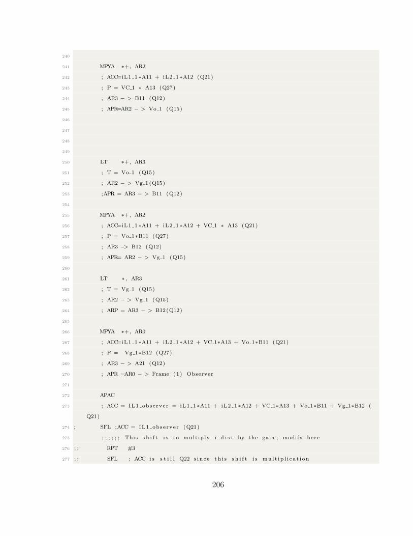
240
241 MPYA ∗+, AR2
242 ; ACC=iL1 1 ∗A11 + iL2 1 ∗A12 (Q21)
243 ; P = VC 1 ∗ A13 (Q27)
244 ; AR3 − > B11 (Q12)
245 ; APR=AR2 − > Vo 1 (Q15)
246
247
248
249
250 LT ∗+, AR3
251 ; T = Vo 1 (Q15)
252 ; AR2 − > Vg 1 (Q15)
253 ;APR = AR3 − > B11 (Q12)
254
255 MPYA ∗+, AR2
256 ; ACC=iL1 1 ∗A11 + iL2 1 ∗A12 + VC 1 ∗ A13 (Q21)
257 ; P = Vo 1∗B11 (Q27)
258 ; AR3 −> B12 (Q12)
259 ; APR= AR2 − > Vg 1 (Q15)
260
261 LT ∗ , AR3
262 ; T = Vg 1 (Q15)
263 ; AR2 − > Vg 1 (Q15)
264 ; ARP = AR3 − > B12(Q12)
265
266 MPYA ∗+, AR0
267 ; ACC=iL1 1 ∗A11 + iL2 1 ∗A12 + VC 1∗A13 + Vo 1∗B11 (Q21)
268 ; P = Vg 1∗B12 (Q27)
269 ; AR3 − > A21 (Q12)
270 ; APR =AR0 − > Frame (1) Observer
271
272 APAC
273 ; ACC = IL1 obse rve r = iL1 1 ∗A11 + iL2 1 ∗A12 + VC 1∗A13 + Vo 1∗B11 + Vg 1∗B12 (
Q21)
274 ; SFL ;ACC = IL1 obse rve r (Q21)
275 ; ; ; ; ; ; This s h i f t i s to mult ip ly i d i s t by the gain , modify here
276 ; ; RPT #3
277 ; ; SFL ; ACC i s s t i l l Q22 s i n c e t h i s s h i f t i s mu l t i p l i c a t i o n
206
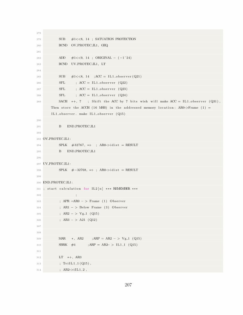
278
279 SUB #1<<8, 14 ; SATUATION PROTECTION
280 BCND OV PROTEC IL1 , GEQ
281
282 ADD #1<<9, 14 ; ORIGINAL − (−1ˆ24)
283 BCND UV PROTEC IL1 , LT
284
285 SUB #1<<8, 14 ;ACC = IL1 obse rve r (Q21)
286 SFL ; ACC = IL1 obse rve r (Q22)
287 SFL ; ACC = IL1 obse rve r (Q23)
288 SFL ; ACC = IL1 obse rve r (Q24)
289 SACH ∗+, 7 ; Sh i f t the ACC by 7 b i t s wish w i l l make ACC = IL1 obse rve r (Q31) ,
Then s t o r e the ACCH (16 MSB) in the addressed memory l o c a t i o n : AR0−>Frame (1) =
IL1 obse rve r . make IL1 obse rve r (Q15)
290
291 B END PROTEC IL1
292
293 OV PROTEC IL1 :
294 SPLK #32767 , ∗+ ; AR0−> i d i s t = RESULT
295 B END PROTEC IL1
296
297 UV PROTEC IL1 :
298 SPLK #−32768, ∗+ ; AR0−> i d i s t = RESULT
299
300 END PROTEC IL1 :
301 ; s t a r t c a l c u l a t i o n f o r IL2 [ n ] ∗∗∗ REMEMBER ∗∗∗
302 ;
303 ; APR =AR0 − > Frame (1) Observer
304 ; AR1 − > Below Frame (3) Observer
305 ; AR2 − > Vg 1 (Q15)
306 ; AR3 − > A21 (Q12)
307
308
309 MAR ∗ , AR2 ;ARP = AR2 − > Vg 1 (Q15)
310 SBRK #4 ;ARP = AR2− > IL1 1 (Q15)
311
312 LT ∗+, AR3
313 ; T=i IL1 1 (Q15) ,
314 ; AR2−>i IL1 2 ,
207

315 ; APR=AR3−>A21(Q12)
316 ; AR0−>(Frame 2)
317
318 MPY ∗+, AR2 ; P=T∗(∗AR3) i . e . P=i IL1 1 ∗A21 (Q27)
319 ; AR3 −> A22
320 ; APR = AR2 −> iL2 1
321 PAC ; ACC = ( i IL1 1 ∗A21)>>6, (Q21)
322
323
324 LT ∗+, AR3
325 ; T=iL2 1 (Q15) ,
326 ; AR2−>VC 1
327 ; APR=AR3 −> A22(Q12)
328 ; AR0−>(Frame 2)
329
330 MPY ∗+, AR2
331 ; P = ( iL2 1 ∗A22) (Q27)
332 ; AR3 −> A23(Q12)
333 ; ARP = AR2 − > VC 1 (Q15) ,
334
335 LT ∗+, AR3
336 ; T = VC 1 (Q15)
337 ; AR2 −> Vo 1 (Q15)
338 ; ARP = AR3 − > A23 (Q12)
339
340 MPYA ∗+, AR2
341 ; ACC = ( i IL1 1 ∗A21) + ( iL2 1 ∗A22) (Q21)
342 ; P = VC 1 ∗ A23 (Q27)
343 ; AR3 − > B21 (Q12)
344 ; APR = AR2 − > Vo 1 (Q15)
345
346
347 LT ∗+, AR3
348 ; T = Vo 1 (Q15)
349 ; AR2 − > Vg 1 (Q15)
350 ; APR = AR3 − > B21 (Q12)
351
352
353 MPYA ∗+, AR2
208
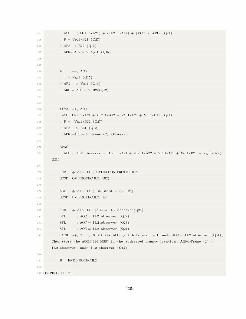
354 ; ACC = ( i IL1 1 ∗A21) + ( iL2 1 ∗A22) + (VC 1 ∗ A23) (Q21)
355 ; P = Vo 1∗B21 (Q27)
356 ; AR3 −> B22 (Q12)
357 ; APR= AR2 − > Vg 1 (Q15)
358
359
360 LT ∗−, AR3
361 ; T = Vg 1 (Q15)
362 ; AR2 − > Vo 1 (Q15)
363 ; ARP = AR3 − > B22(Q12)
364
365
366 MPYA ∗+, AR0
367 ;ACC=i IL1 1 ∗A21 + iL2 1 ∗A22 + VC 1∗A23 + Vo 1∗B21 (Q21)
368 ; P = Vg 1∗B22 (Q27)
369 ; AR3 − > A31 (Q12)
370 ; APR =AR0 − > Frame (2) Observer
371
372 APAC
373 ; ACC = IL2 obse rve r = i IL1 1 ∗A21 + iL2 1 ∗A22 + VC 1∗A23 + Vo 1∗B21 + Vg 1∗B22(
Q21)
374
375 SUB #1<<8, 14 ; SATUATION PROTECTION
376 BCND OV PROTEC IL2 , GEQ
377
378 ADD #1<<9, 14 ; ORIGINAL − (−1ˆ24)
379 BCND UV PROTEC IL2 , LT
380
381 SUB #1<<8, 14 ;ACC = IL2 obse rve r (Q21)
382 SFL ; ACC = IL2 obse rve r (Q22)
383 SFL ; ACC = IL2 obse rve r (Q23)
384 SFL ; ACC = IL2 obse rve r (Q24)
385 SACH ∗+, 7 ; Sh i f t the ACC by 7 b i t s wish w i l l make ACC = IL2 obse rve r (Q31) ,
Then s t o r e the ACCH (16 MSB) in the addressed memory l o c a t i o n : AR0−>Frame (2) =
IL2 obse rve r . make IL2 obse rve r (Q15)
386
387 B END PROTEC IL2
388
389 OV PROTEC IL2 :
209

390 SPLK #32767 , ∗+ ; Frame (2) = Max Po s i t i v e 16−b i t s value , AR0−> Frame (3)
391 B END PROTEC IL2
392
393 UV PROTEC IL2 :
394 SPLK #−32768, ∗+ ; Frame (2) = Max Negative 16−b i t s value , AR0−> Frame (3)
395
396 END PROTEC IL2 :
397 ; s t a r t c a l c u l a t i o n f o r VC[ n ] ∗∗∗ REMEMBER ∗∗∗
398
399 ; APR =AR0 − > Frame (3) Observer
400 ; AR1 − > Below Frame (3) Observer
401 ; AR2 − > Vo 1 (Q15)
402 ; AR3 − > A31 (Q12)
403
404
405 MAR ∗ , AR2 ;ARP = AR2 − > Vo 1 (Q15)
406 SBRK #3 ;ARP = AR2− > IL1 1 (Q15)
407
408 LT ∗+, AR3
409 ; T=i IL1 1 (Q15) ,
410 ; AR2−>i IL1 2 ,
411 ; APR=AR3−>A31(Q12)
412 ; AR0−>(Frame 3)
413
414 MPY ∗+, AR2 ; P=T∗(∗AR3) i . e . P=i IL1 1 ∗A31 (Q27)
415 ; AR3 −> A32
416 ; APR = AR2 −> iL2 1
417 PAC ; ACC = ( i IL1 1 ∗A31)>>6, (Q21)
418
419
420 LT ∗+, AR3
421 ; T=iL2 1 (Q15) ,
422 ; AR2−>VC 1
423 ; APR=AR3 −> A32(Q12)
424 ; AR0−>(Frame 3)
425
426 MPY ∗+, AR2
427 ; P = ( iL2 1 ∗A32) (Q27)
428 ; AR3 −> A33(Q12)
210
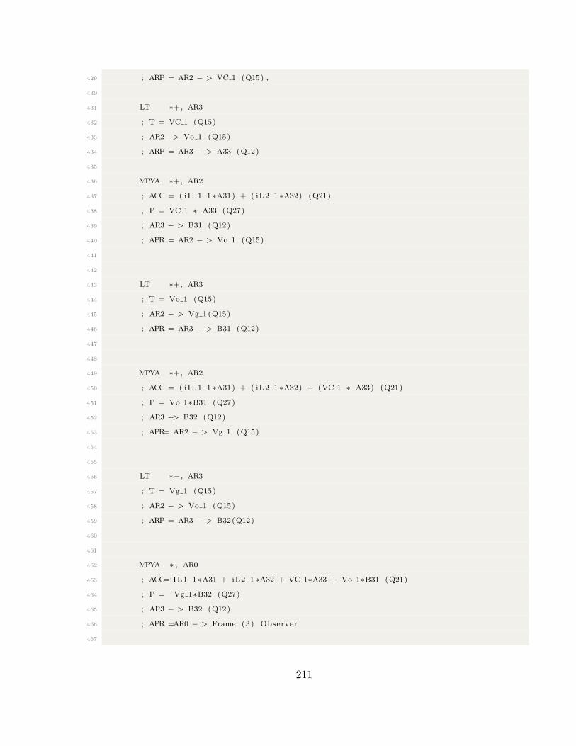
429 ; ARP = AR2 − > VC 1 (Q15) ,
430
431 LT ∗+, AR3
432 ; T = VC 1 (Q15)
433 ; AR2 −> Vo 1 (Q15)
434 ; ARP = AR3 − > A33 (Q12)
435
436 MPYA ∗+, AR2
437 ; ACC = ( i IL1 1 ∗A31) + ( iL2 1 ∗A32) (Q21)
438 ; P = VC 1 ∗ A33 (Q27)
439 ; AR3 − > B31 (Q12)
440 ; APR = AR2 − > Vo 1 (Q15)
441
442
443 LT ∗+, AR3
444 ; T = Vo 1 (Q15)
445 ; AR2 − > Vg 1 (Q15)
446 ; APR = AR3 − > B31 (Q12)
447
448
449 MPYA ∗+, AR2
450 ; ACC = ( i IL1 1 ∗A31) + ( iL2 1 ∗A32) + (VC 1 ∗ A33) (Q21)
451 ; P = Vo 1∗B31 (Q27)
452 ; AR3 −> B32 (Q12)
453 ; APR= AR2 − > Vg 1 (Q15)
454
455
456 LT ∗−, AR3
457 ; T = Vg 1 (Q15)
458 ; AR2 − > Vo 1 (Q15)
459 ; ARP = AR3 − > B32(Q12)
460
461
462 MPYA ∗ , AR0
463 ; ACC=i IL1 1 ∗A31 + iL2 1 ∗A32 + VC 1∗A33 + Vo 1∗B31 (Q21)
464 ; P = Vg 1∗B32 (Q27)
465 ; AR3 − > B32 (Q12)
466 ; APR =AR0 − > Frame (3) Observer
467
211

468 APAC
469 ; ACC = VC observer = i IL1 1 ∗A31 + iL2 1 ∗A32 + VC 1∗A33 + Vo 1∗B31 + Vg 1∗B32(Q21
)
470
471 SUB #1<<8, 14 ; SATUATION PROTECTION
472 BCND OV PROTEC VC, GEQ
473
474 ADD #1<<9, 14 ; ORIGINAL − (−1ˆ24)
475 BCND UV PROTEC VC, LT
476
477 SUB #1<<8, 14 ;ACC = VC observer (Q21)
478 SFL ; ACC = VC observer (Q22)
479 SFL ; ACC = VC observer (Q23)
480 SFL ; ACC = VC observer (Q24)
481 SACH ∗ , 7 ; S h i f t the ACC by 7 b i t s wish w i l l make ACC = VC observer (Q31) ,
Then s t o r e the ACCH (16 MSB) in the addressed memory l o c a t i o n : AR0−>Frame (3) =
VC observer . make VC observer (Q15)
482
483 B END PROTEC VC
484
485 OV PROTEC VC:
486 SPLK #32767 , ∗ ; Frame (3) = Max Po s i t i v e 16−b i t s value , AR0−> Frame (3)
487 B END PROTEC VC
488
489 UV PROTEC VC:
490 SPLK #−32768, ∗ ; Frame (3) = Max Negative 16−b i t s value , AR0−> Frame (3)
491
492 END PROTEC VC:
493 ; Update the va lue s in the memory ∗∗∗ REMEMBER ∗∗∗
494
495 ; APR =AR0 − > Frame (3) Observer
496 ; AR1 − > Below Frame (3) Observer
497 ; AR2 − > Vo 1 (Q15)
498 ; AR3 − > B32 (Q12)
499
500
501 LACC ∗−, AR2
502 ; ACC = Frame (3) = VC[ n ]
503 ; AR0 − > Frame (2) = IL2 [ n ]
212
504 ; ARP = AR2 − > Vo 1
505
506 MAR ∗−
507 ; ARP = AR2 − > Vc 1
508
509 SACL ∗−, AR0
510 ; Vc 1 = VC[ n ]
511 ; AR2 − > IL2 1
512 ; APR = AR0 − > Frame (2) = IL2 [ n ]
513
514 LACC ∗−, AR2
515 ; ACC = Frame (2) = IL2 [ n ]
516 ; AR0 − > Frame (1) = IL1 [ n ]
517 ; ARP = AR2 − > IL2 1
518
519 SACL ∗−, AR0
520 ; IL2 1 = IL2 [ n ]
521 ; AR2 − > IL1 1
522 ; APR = AR0 − > Frame (1) = IL1 [ n ]
523
524 LACC ∗ , AR2
525 ; ACC = Frame (1) = IL1 [ n ]
526 ; AR0 − > Frame (1) = IL1 [ n ]
527 ; ARP = AR2 − > IL1 1
528
529 SACL ∗ , AR4
530 ; IL1 1 = IL1 [ n ]
531 ; APR = AR2 − > IL1 1
532 ; AR0 − > Frame (1) = IL1 [ n ]
533
534
535 SBRK #30 ; ARP = AR4 −> piVgr id
536 LAR AR4,∗ ; AR4 = ∗(AR4) = ∗( piVgr id ) = Vgrid ;
537 LACC ∗ ,AR2 ; ACC=Vgrid , AR2 −> i IL1 1
538 ADRK #4 ; APR = AR2 − > Observer .Vg
539 SACL ∗+,AR2 ; Observer .Vg = Vgrid
540 ; AR3 − > A11
541 ; APR=AR2 − > i IL1 1
542
213
543
544 ; Re ADDED WE NEED TO UPDATE inv1 . cn t l 2 . i I L1 ob s e r v e r and inv1 . cn t l 2 . i I L2 ob s e r v e r
545 ; b e f o r e CALCULATING THE DUTY CYCLE
546 SBRK #32
547 ; ; APR = AR2 − > inv1 . cn t l 2 . i I L1 ob s e r v e r
548 ;
549 MAR ∗ , AR0
550 ; ; APR = AR0 − > Frame (1) = IL1 [ n ]
551 ;
552 LACC ∗+, AR2
553 ; ; ACC = Frame (1) = IL1 [ n ]
554 ; ; AR0 − > Frame (2) = IL2 [ n ]
555 ; ; ARP = AR2 − > inv1 . cn t l 2 . i I L1 ob s e r v e r
556 ;
557 SACL ∗+, AR0
558 ; ; inv1 . cn t l 2 . i I L1 ob s e r v e r = IL1 [ n ]
559 ; ; AR2 − > inv1 . cn t l 2 . i I L2 ob s e r v e r
560 ; ; APR = AR0 − > Frame (2) = IL2 [ n ]
561 ;
562 LACC ∗ , AR2
563 ; ; ACC = Frame (2) = IL2 [ n ]
564 ; ; AR0 − > Frame (2) = IL2 [ n ]
565 ; ; ARP = AR2 − > inv1 . cn t l 2 . i I L2 ob s e r v e r
566 ;
567 SACL ∗−, AR1
568 ; ; inv1 . cn t l 2 . i I L2 ob s e r v e r = IL2 [ n ]
569 ; ; AR2 − > inv1 . cn t l 2 . i I L1 ob s e r v e r
570 ; ; APR = AR1 − > below Frame (3)
571
572 ob s e r v e rCa l c e x i t :
573
574 CLRC OVM
575 SPM 0
576
577 ; MAR ∗ ,AR1 ; can be removed i f t h i s cond i t i on i s met on
578 ; every path to t h i s code .
579 ; s e t ARP = SP be f o r e you e x i t .
580 SBRK #( ob s e r v e rCa l c f r ame s i z e +1)
581 ; APR = AR1 − > Frame adre s s o f i n v 1 cn t l 2 subrout ine
214

582
583 ; d e a l l o c a t e frame , po int to saved FP
584 LAR AR0, ∗− ; r e s t o r e frame po in t e r
585 ; AR0 − > Frame (1) INV1 CNTL2 subrout ine
586 ; APR = AR1 − > Return adre s s o f i n v 1 cn t l 2 subrout ine
587
588
589 PSHD ∗ ; push re turn address on hardware s tack
590
591
592
593
594 RET
595
596 . end
215

Vita
Candidate’s full name: Haider Mohomad AR
University attended:
Bachelor of Science in Engineering (May 2009)
Department of Electrical and Computer Engineering
University of New Brunswick
Fredericton, NB, Canada
Master of Science in Engineering (Oct 2012)
Department of Electrical and Computer Engineering
University of New Brunswick
Fredericton, NB, Canada
Doctor of Philosophy in Engineering (Candidate)
Department of Electrical and Computer Engineering
University of New Brunswick
Fredericton, NB, Canada
Publications:
1. H. Mohomad, S. A. Saleh, R. Shao and L. Chang, Dead-Beat Current Controller
for Voltage Source Inverter with LCL Grid-Tied Filter 2018 IEEE Energy Conversion
Congress and Exposition, Portland, OR, 2018.
2. H. Mohomad, S. A. M. Saleh, L. Chang, Disturbance Estimator-Based Pre-
dictive Current Controller for Single-Phase Interconnected PV Systems, in IEEE
Transactions on Industry Applications, vol. 53, no. 5, pp.4201-4209, Sept.-Oct. 2017.
3. H. Mohomad, S. A. Saleh and L. Chang, ”Disturbance-estimator predictive
current controller for 1φ interconnected PV systems,” 2017 IEEE/IAS 53rd Industrial
and Commercial Power Systems Technical Conference (ICPS), Niagara Falls, ON, 2017,
pp. 1-8.
4. M. A. R. Haider, S. A. Saleh, R. Shao and L. Chang, ”Robust current controller for
grid-connected voltage source inverter,” 2017 IEEE 8th International Symposium on
Power Electronics for Distributed Generation Systems (PEDG), Florianopolis, Brazil,
2017, pp. 1-7.
5. R. H. Mohomad, S. A. Saleh, L. Chang, R. Shao and S. Xu, ”Observer-based
predictive current controller for grid-connected single-phase wind converter,” 2017 IEEE
Applied Power Electronics Conference and Exposition (APEC), Tampa, FL, 2017, pp.
2767-2772.
6. H. Mohomad A R, L. Chang and R. Shao, ”Impulsive noise modeling in single

phase grid-connected power converter,” 2016 IEEE 7th International Symposium on
Power Electronics for Distributed Generation Systems (PEDG), Vancouver, BC, 2016,
pp. 1-5.
7. H. Mohomad A R, L. Chang and R. Shao, ”The time delay effect in the pre-
dictive current controller of single-phase grid-connected power converter,” 2016 IEEE
7th International Symposium on Power Electronics for Distributed Generation Systems
(PEDG), Vancouver, BC, 2016, pp. 1-7.
8. R. Haider Mohomad, C. P. Diduch, Y. Biletskiy, R. Shao and L. Chang, ”Re-
moval of measurement noise spikes in grid-connected power converters,” 2013 4th IEEE
International Symposium on Power Electronics for Distributed Generation Systems
(PEDG), Rogers, AR, 2013, pp. 1-5.
9. H. Mohammad, C. P. Diduch, Y. Biletskiy and L. Chang, ”Filtering out spikes
from sensors in power converters system using discrete wavelet transform,” 2012 25th
IEEE Canadian Conference on Electrical and Computer Engineering (CCECE), Mon-
treal, QC, 2012, pp. 1-3.
Academic Awards:
1. Best paper award at the 8th International Symposium on Power Electronics for Dis-
tributed Generation Systems (PEDG 2017) - 17th 20th of April, 2017, in Florianpolis,
Brazil.
2. Board of Governors Merit Awards for Graduate Studies, 2011.