Digole 128x64Dots Serial/Parallel LCD
40
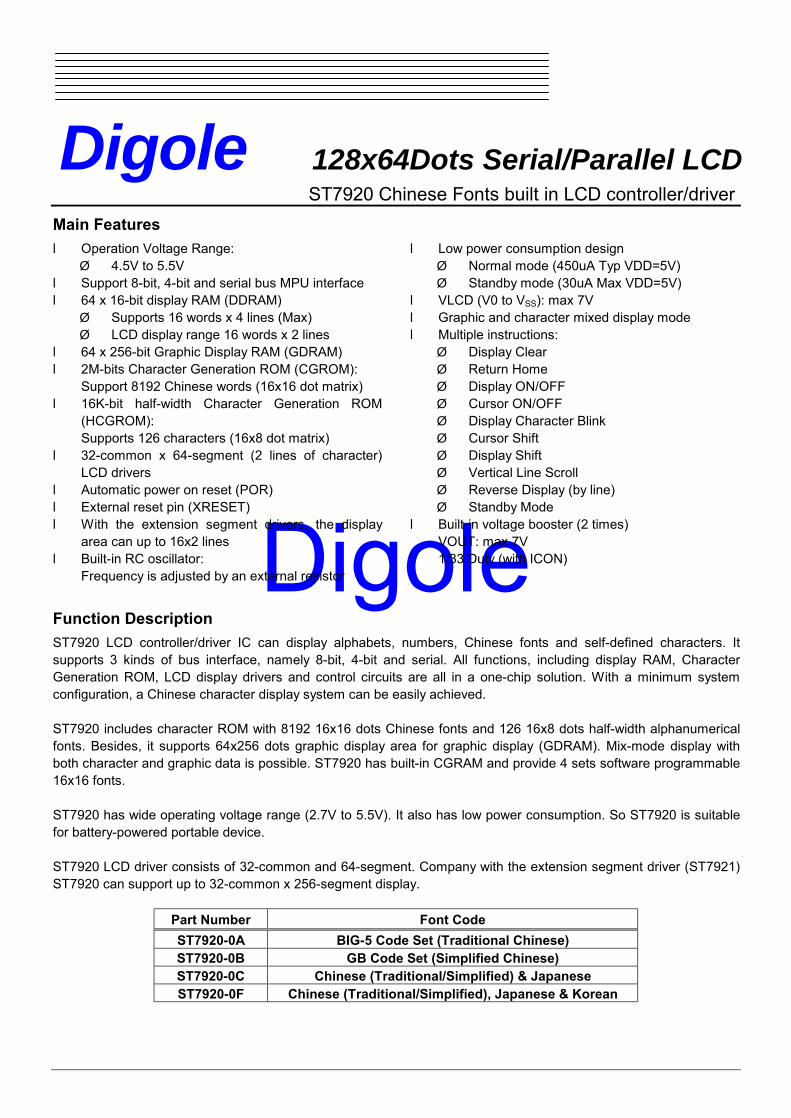
Digole Digole 128x64Dots Serial/Parallel LCD ST7920 Chinese Fonts built in LCD controller/driver Main Features l Operation Voltage Range: 4.5V to 5.5V l Support 8-bit, 4-bit and serial bus MPU interface l 64 x 16-bit display RAM (DDRAM) Supports 16 words x 4 lines (Max) LCD display range 16 words x 2 lines l 64 x 256-bit Graphic Display RAM (GDRAM) l 2M-bits Character Generation ROM (CGROM): Support 8192 Chinese words (16x16 dot matrix) l 16K-bit half-width Character Generation ROM (HCGROM): Supports 126 characters (16x8 dot matrix) l 32-common x 64-segment (2 lines of character) LCD drivers l Automatic power on reset (POR) l External reset pin (XRESET) l With the extension segment drivers, the display area can up to 16x2 lines l Built-in RC oscillator: Frequency is adjusted by an external resistor l Low power consumption design Normal mode (450uA Typ VDD=5V) Standby mode (30uA Max VDD=5V) l VLCD (V0 to V SS ): max 7V l Graphic and character mixed display mode l Multiple instructions: Display Clear Return Home Display ON/OFF Cursor ON/OFF Display Character Blink Cursor Shift Display Shift Vertical Line Scroll Reverse Display (by line) Standby Mode l Built-in voltage booster (2 times) VOUT: max 7V l 1/33 Duty (with ICON) Function Description ST7920 LCD controller/driver IC can display alphabets, numbers, Chinese fonts and self-defined characters. It supports 3 kinds of bus interface, namely 8-bit, 4-bit and serial. All functions, including display RAM, Character Generation ROM, LCD display drivers and control circuits are all in a one-chip solution. With a minimum system configuration, a Chinese character display system can be easily achieved. ST7920 includes character ROM with 8192 16x16 dots Chinese fonts and 126 16x8 dots half-width alphanumerical fonts. Besides, it supports 64x256 dots graphic display area for graphic display (GDRAM). Mix-mode display with both character and graphic data is possible. ST7920 has built-in CGRAM and provide 4 sets software programmable 16x16 fonts. ST7920 has wide operating voltage range (2.7V to 5.5V). It also has low power consumption. So ST7920 is suitable for battery-powered portable device. ST7920 LCD driver consists of 32-common and 64-segment. Company with the extension segment driver (ST7921) ST7920 can support up to 32-common x 256-segment display. Part Number Font Code ST7920-0A BIG-5 Code Set (Traditional Chinese) ST7920-0B GB Code Set (Simplified Chinese) ST7920-0C Chinese (Traditional/Simplified) & Japanese ST7920-0F Chinese (Traditional/Simplified), Japanese & Korean
Transcript of Digole 128x64Dots Serial/Parallel LCD
Digole
Digole 128x64Dots Serial/Parallel LCD ST7920 Chinese Fonts built in LCD controller/driver
Main Features l Operation Voltage Range:
Ø 4.5V to 5.5V l Support 8-bit, 4-bit and serial bus MPU interface l 64 x 16-bit display RAM (DDRAM)
Ø Supports 16 words x 4 lines (Max) Ø LCD display range 16 words x 2 lines
l 64 x 256-bit Graphic Display RAM (GDRAM) l 2M-bits Character Generation ROM (CGROM):
Support 8192 Chinese words (16x16 dot matrix) l 16K-bit half-width Character Generation ROM
(HCGROM): Supports 126 characters (16x8 dot matrix)
l 32-common x 64-segment (2 lines of character) LCD drivers
l Automatic power on reset (POR) l External reset pin (XRESET) l With the extension segment drivers, the display
area can up to 16x2 lines l Built-in RC oscillator:
Frequency is adjusted by an external resistor
l Low power consumption design Ø Normal mode (450uA Typ VDD=5V) Ø Standby mode (30uA Max VDD=5V)
l VLCD (V0 to VSS): max 7V l Graphic and character mixed display mode l Multiple instructions:
Ø Display Clear Ø Return Home Ø Display ON/OFF Ø Cursor ON/OFF Ø Display Character Blink Ø Cursor Shift Ø Display Shift Ø Vertical Line Scroll Ø Reverse Display (by line) Ø Standby Mode
l Built-in voltage booster (2 times) VOUT: max 7V
l 1/33 Duty (with ICON)
Function Description ST7920 LCD controller/driver IC can display alphabets, numbers, Chinese fonts and self-defined characters. It supports 3 kinds of bus interface, namely 8-bit, 4-bit and serial. All functions, including display RAM, Character Generation ROM, LCD display drivers and control circuits are all in a one-chip solution. With a minimum system configuration, a Chinese character display system can be easily achieved. ST7920 includes character ROM with 8192 16x16 dots Chinese fonts and 126 16x8 dots half-width alphanumerical fonts. Besides, it supports 64x256 dots graphic display area for graphic display (GDRAM). Mix-mode display with both character and graphic data is possible. ST7920 has built-in CGRAM and provide 4 sets software programmable 16x16 fonts. ST7920 has wide operating voltage range (2.7V to 5.5V). It also has low power consumption. So ST7920 is suitable for battery-powered portable device. ST7920 LCD driver consists of 32-common and 64-segment. Company with the extension segment driver (ST7921) ST7920 can support up to 32-common x 256-segment display.
Part Number Font Code ST7920-0A BIG-5 Code Set (Traditional Chinese) ST7920-0B GB Code Set (Simplified Chinese) ST7920-0C Chinese (Traditional/Simplified) & Japanese ST7920-0F Chinese (Traditional/Simplified), Japanese & Korean
Digole
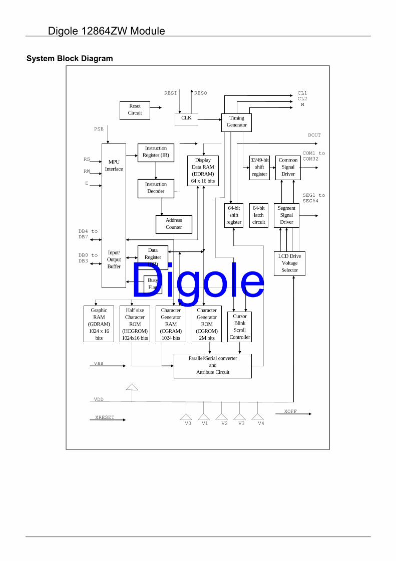
System Block Diagram
Timing
Generator
33/49-bit
shift
register
Common
Signal
Driver
Display
Data RAM
(DDRAM)
64 x 16 bits
64-bit
latch
circuit
Segment
Signal
Driver
64-bit
shift
register
LCD Drive
Voltage
Selector
CLK
Instruction
Register (IR)
Instruction
Decoder
Reset
Circuit
MPU
Interface
Input/
Output
Buffer
Address
Counter
Character
Generator
ROM
(CGROM)
2M bits
Character
Generator
RAM
(CGRAM)
1024 bits
Cursor
Blink
Scroll
Controller
Data
Register
(DR)
Busy
Flag
Parallel/Serial converter
and
Attribute Circuit
VDD
V0 V1 V2 V3 V4
RESI RESO CL1 CL2 M
DOUT
COM1 to COM32
SEG1 to SEG64
RS
RW
E
DB4 to DB7
DB0 to DB3
Half size
Character
ROM
(HCGROM)
1024x16 bits
XRESET
Graphic
RAM
(GDRAM)
1024 x 16
bits
XOFF
Vss
PSB
Digole 12864ZW Module
Digole
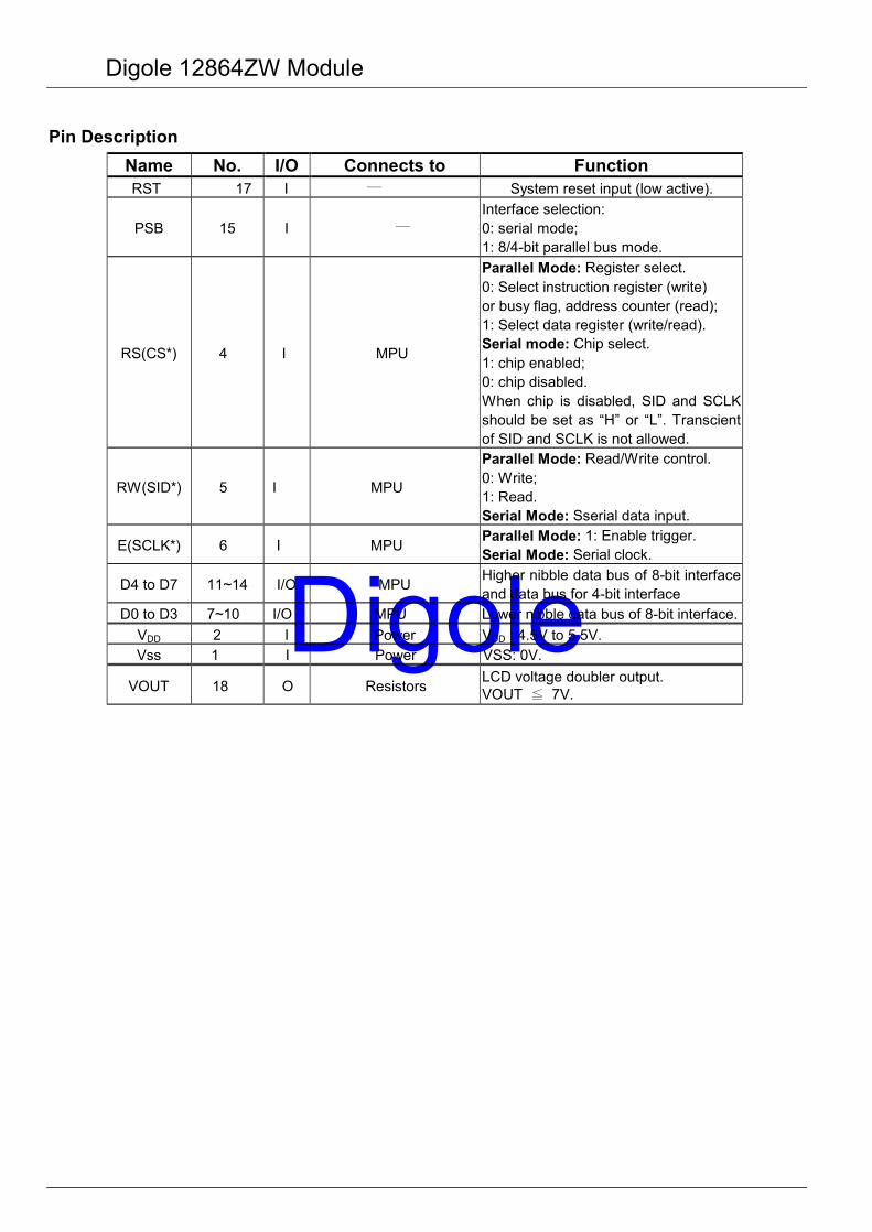
Pin Description Name No. I/O Connects to Function
RST 17 I ― System reset input (low active).
PSB 15 I ― Interface selection: 0: serial mode; 1: 8/4-bit parallel bus mode.
RS(CS*) 4 I MPU
Parallel Mode: Register select. 0: Select instruction register (write) or busy flag, address counter (read); 1: Select data register (write/read). Serial mode: Chip select. 1: chip enabled; 0: chip disabled. When chip is disabled, SID and SCLK should be set as “H” or “L”. Transcient of SID and SCLK is not allowed.
RW(SID*) 5 I MPU
Parallel Mode: Read/Write control. 0: Write; 1: Read. Serial Mode: Sserial data input.
E(SCLK*) 6 I MPU Parallel Mode: 1: Enable trigger. Serial Mode: Serial clock.
D4 to D7 11~14 I/O MPU Higher nibble data bus of 8-bit interface and data bus for 4-bit interface
D0 to D3 7~10 I/O MPU Lower nibble data bus of 8-bit interface. VDD 2 I Power VDD : 4.5V to 5.5V. Vss 1 I Power VSS: 0V.
VOUT 18 O Resistors LCD voltage doubler output. VOUT ≦ 7V.
Digole 12864ZW Module
Digole
Function Description
System interface
ST7920 supports 3 kinds of bus interface to communicate with MPU: 8-bit parallel, 4-bit parallel and clock synchronized serial interface. Parallel interface is selected by PSB=”1” and serial interface is by PSB=”0”. 8-bit / 4-bit interface is selected by function set instruction DL bit. Two 8-bit registers (Data Register DR and Instruction Register IR) are used in ST7920 to access DRAM or Register. Data Register (DR) can access DDRAM, CGRAM and GDRAM through the address pointer implemented by Address Counter (AC). Instruction Register (IR) stores the instruction sent by MPU to ST7920. 4 kinds of parallel interface access mode can be selected through RS and RW:
RS RW Description L L MPU write instruction to instruction register (IR) L H MPU read busy flag (BF) and address counter (AC) H L MPU write data to data register (DR) H H MPU read data from data register (DR)
* The serial interface access modes do not have Read operation.
Busy Flag (BF)
ST7920 needs a process time for any received instruction. Before finishing the received instruction, any further instruction is not accepted. The process time of each instruction is not equal and the internal process is finished or not can be determined by the BF. Internal operation is in progress while BF=”1”, that means ST7920 is in busy state. No further instructions will be accepted until BF=”0”. MPU must check BF to determine whether the internal operation is finished or not before issuing instruction.
Address Counter (AC)
Address Counter (AC) is used as the address pointer of DDRAM, CGRAM and GDRAM. (AC) can be set by instruction. After that, accesses (Read/Write operations) to the memories, such as DDRAM, CGRAM or GDRAM, (AC) will be increased or decreased by 1 (according to the setting in “Entry Mode Set” Register). When RS=”0”, RW=”1” and E=”1” the value of (AC) will be output to DB6~DB0.
Character Generation ROM (CGROM) and Half-width Character Generation ROM (HCGROM)
ST7920 is built in a Character Generation ROM (CGROM) to provide 8192 16x16 character fonts and a Half-width Character Generation ROM to provide 126 8x16 alphanumeric characters. It is easy to support multi-language applications such as Chinese and English. Two consecutive bytes are used to specify one 16x16 character or two 8x16 half-width characters. Character codes are written into DDRAM and the corresponding fonts are mapped from CGROM or HCGROM to the display drivers.
Character Generation RAM (CGRAM)
ST7920 is built in a Character Generation RAM (CGRAM) to support user-defined fonts. Four sets of 16x16 bit-maped RAM spaces are available. These user-defined fonts are displayed the same ways as CGROM fonts by writing the related character code into the DDRAM.
Digole 12864ZW Module
Digole
Display Data RAM (DDRAM)
There are 64x2 bytes RAM spaces for the Display Data RAM. It can store display data such as 16 characters (16x16) by 4 lines or 32 characters (8x16) by 4 lines. However, only 2 character-lines (maximum 32 common outputs) can be displayed at one time. Character codes stored in DDRAM will refer to the fonts specified by CGROM, HCGROM and CGRAM. ST7920 can display half-width HCGROM fonts, user-defined CGRAM fonts and full 16x16 CGROM fonts. The character codes in 0000H~0006H will use user-defined fonts in CGRAM. The character codes in 02H~7FH will use half-width alpha numeric fonts. The character code larger than A1H will be treated as 16x16 fonts and will be combined with the next byte automatically. The 16x16 BIG5 fonts are stored in A140H~D75FH while the 16x16 GB fonts are stored in A1A0H~F7FFH. In short: 1. To display HCGROM fonts:
Write 2 bytes of data into DDRAM to display two 8x16 fonts. Each byte represents 1 character. The data is among 02H~7FH.
2. To display CGRAM fonts: Write 2 bytes of data into DDRAM to display one 16x16 font. Only 0000H, 0002H, 0004H and 0006H are acceptable.
3. To display CGROM fonts: Write 2 bytes of data into DDRAM to display one 16x16 font. A140H~D75FH are BIG5 code, A1A0H~F7FFH are GB code.
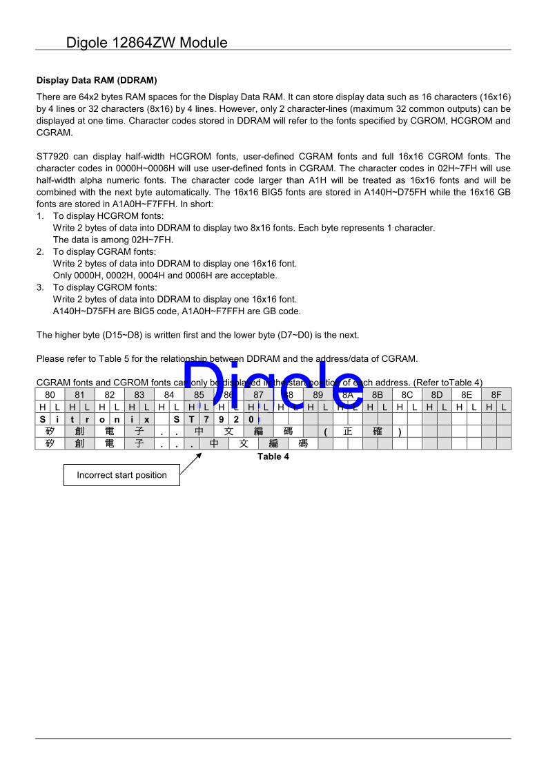
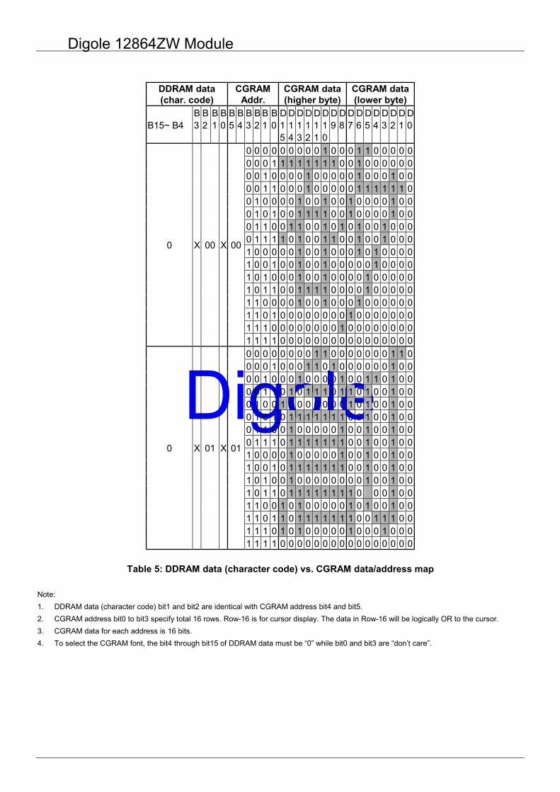
The higher byte (D15~D8) is written first and the lower byte (D7~D0) is the next. Please refer to Table 5 for the relationship between DDRAM and the address/data of CGRAM. CGRAM fonts and CGROM fonts can only be displayed in the start position of each address. (Refer toTable 4)
80 81 82 83 84 85 86 87 88 89 8A 8B 8C 8D 8E 8F H L H L H L H L H L H L H L H L H L H L H L H L H L H L H L H L S i t r o n i x S T 7 9 2 0 矽 創 電 子 . . 中 文 編 碼 ( 正 確 ) 矽 創 電 子 . . . 中 文 編 碼
Table 4
Incorrect start position
Digole 12864ZW Module
Digole
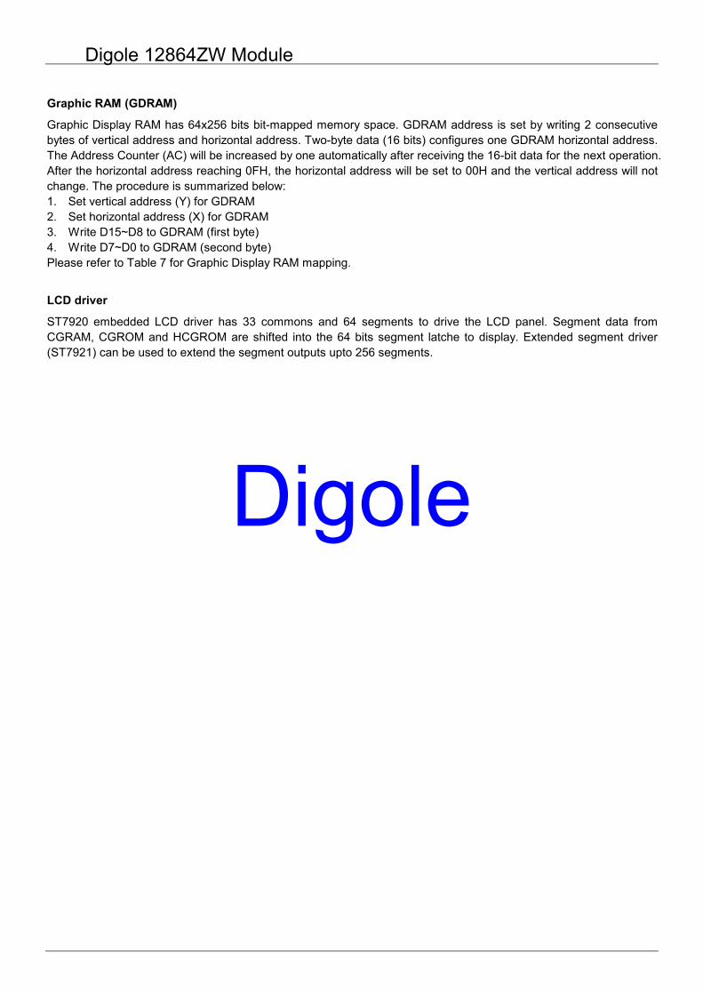
Graphic RAM (GDRAM)
Graphic Display RAM has 64x256 bits bit-mapped memory space. GDRAM address is set by writing 2 consecutive bytes of vertical address and horizontal address. Two-byte data (16 bits) configures one GDRAM horizontal address. The Address Counter (AC) will be increased by one automatically after receiving the 16-bit data for the next operation. After the horizontal address reaching 0FH, the horizontal address will be set to 00H and the vertical address will not change. The procedure is summarized below: 1. Set vertical address (Y) for GDRAM 2. Set horizontal address (X) for GDRAM 3. Write D15~D8 to GDRAM (first byte) 4. Write D7~D0 to GDRAM (second byte) Please refer to Table 7 for Graphic Display RAM mapping.
LCD driver
ST7920 embedded LCD driver has 33 commons and 64 segments to drive the LCD panel. Segment data from CGRAM, CGROM and HCGROM are shifted into the 64 bits segment latche to display. Extended segment driver (ST7921) can be used to extend the segment outputs upto 256 segments.
Digole 12864ZW Module
Digole
DDRAM data (char. code)
CGRAM Addr.
CGRAM data (higher byte)
CGRAM data (lower byte)
B15~ B4 B3
B2
B1
B0
B5
B4
B3
B2
B1
B0
D15
D14
D13
D12
D11
D10
D9
D8
D7
D6
D5
D4
D3
D2
D1
D0
0 0 0 0 0 0 0 0 0 1 0 0 0 1 1 0 0 0 0 0 0 0 0 1 1 1 1 1 1 1 1 0 0 1 0 0 0 0 0 0 0 0 1 0 0 0 0 1 0 0 0 0 0 1 0 0 0 1 0 0 0 0 1 1 0 0 0 1 0 0 0 0 0 1 1 1 1 1 1 0 0 1 0 0 0 0 1 0 0 1 0 0 1 0 0 0 0 1 0 0 0 1 0 1 0 0 1 1 1 1 0 0 1 0 0 0 0 1 0 0 0 1 1 0 0 1 1 0 0 1 0 1 0 1 0 0 1 0 0 0 0 1 1 1 1 0 1 0 0 1 1 0 0 1 0 0 1 0 0 0 1 0 0 0 0 0 1 0 0 1 0 0 0 1 0 1 0 0 0 0 1 0 0 1 0 0 1 0 0 1 0 0 0 0 0 1 0 0 0 0 1 0 1 0 0 0 1 0 0 1 0 0 0 0 1 0 0 0 0 0 1 0 1 1 0 0 1 1 1 1 0 0 0 0 1 0 0 0 0 0 1 1 0 0 0 0 1 0 0 1 0 0 0 1 0 0 0 0 0 0 1 1 0 1 0 0 0 0 0 0 0 0 1 0 0 0 0 0 0 0 1 1 1 0 0 0 0 0 0 0 0 1 0 0 0 0 0 0 0 0
0 X 00 X 00
1 1 1 1 0 0 0 0 0 0 0 0 0 0 0 0 0 0 0 0 0 0 0 0 0 0 0 0 1 1 0 0 0 0 0 0 0 1 1 0 0 0 0 1 0 0 0 1 1 0 1 0 0 0 0 0 0 1 0 0 0 0 1 0 0 0 1 0 0 0 0 1 0 0 1 1 0 1 0 0 0 0 1 1 0 1 0 1 1 1 0 1 1 0 1 0 0 1 0 0 0 1 0 0 1 0 0 0 0 0 0 0 1 0 1 0 0 1 0 0 0 1 0 1 0 1 1 1 1 1 1 1 0 0 1 0 0 1 0 0 0 1 1 0 0 1 0 0 0 0 0 1 0 0 1 0 0 1 0 0 0 1 1 1 0 1 1 1 1 1 1 1 0 0 1 0 0 1 0 0 1 0 0 0 0 1 0 0 0 0 0 1 0 0 1 0 0 1 0 0 1 0 0 1 0 1 1 1 1 1 1 1 0 0 1 0 0 1 0 0 1 0 1 0 0 1 0 0 0 0 0 0 0 0 1 0 0 1 0 0 1 0 1 1 0 1 1 1 1 1 1 1 1 0 0 0 1 0 0 1 1 0 0 1 0 1 0 0 0 0 0 1 0 1 0 0 1 0 0 1 1 0 1 1 0 1 1 1 1 1 1 1 0 0 1 1 1 0 0 1 1 1 0 1 0 1 0 0 0 0 0 1 0 0 0 1 0 0 0
0 X 01 X 01
1 1 1 1 0 0 0 0 0 0 0 0 0 0 0 0 0 0 0 0
Table 5: DDRAM data (character code) vs. CGRAM data/address map Note: 1. DDRAM data (character code) bit1 and bit2 are identical with CGRAM address bit4 and bit5. 2. CGRAM address bit0 to bit3 specify total 16 rows. Row-16 is for cursor display. The data in Row-16 will be logically OR to the cursor. 3. CGRAM data for each address is 16 bits. 4. To select the CGRAM font, the bit4 through bit15 of DDRAM data must be “0” while bit0 and bit3 are “don’t care”.
Digole 12864ZW Module
Digole
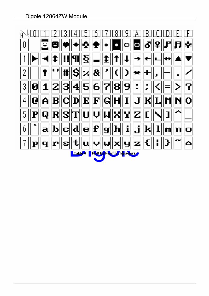
Table 6 16x8 half-width characters
Digole 12864ZW Module
Digole
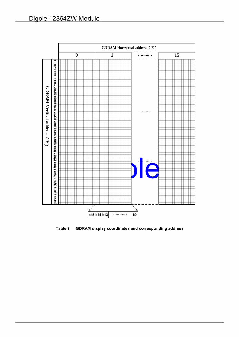
( )GDRAM Horizontal address X
︵
︶
GD
RA
M V
ertical address Y
0 151 ...........0123456789
101112131415161718192021222324252627282930313233343536373839404142434445464748495051525354555657585960616263
...........
...........
...........b14b15 b0b13
Table 7 GDRAM display coordinates and corresponding address
Digole 12864ZW Module
Digole
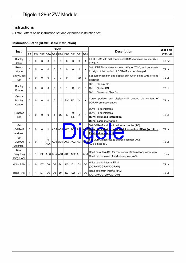
Instructions ST7920 offers basic instruction set and extended instruction set:
Instruction Set 1: (RE=0: Basic Instruction)
Code Inst.
RS RW DB7 DB6 DB5 DB4 DB3 DB2 DB1 DB0 Description Exec time
(540KHZ)
Display Clear
0 0 0 0 0 0 0 0 0 1 Fill DDRAM with "20H" and set DDRAM address counter (AC) to "00H".
1.6 ms
Return Home
0 0 0 0 0 0 0 0 1 X Set DDRAM address counter (AC) to "00H", and put cursor to origin ;the content of DDRAM are not changed
72 us
Entry Mode Set
0 0 0 0 0 0 0 1 I/D S Set cursor position and display shift when doing write or read operation
72 us
Display Control
0 0 0 0 0 0 1 D C B D=1: Display ON C=1: Cursor ON B=1: Character Blink ON
72 us
Cursor Display Control
0 0 0 0 0 1 S/C R/L X X Cursor position and display shift control; the content of DDRAM are not changed
72 us
Function Set
0 0 0 0 1 DL X 0
RE X X
DL=1 8-bit interface DL=0 4-bit interface RE=1: extended instruction RE=0: basic instruction
72 us
Set CGRAM Address.
0 0 0 1 AC5 AC4 AC3 AC2 AC1 AC0 Set CGRAM address to address counter (AC) Make sure that in extended instruction SR=0 (scroll or RAM address select)
72 us
Set DDRAM Address.
0 0 1 0
AC6 AC5 AC4 AC3 AC2 AC1 AC0
Set DDRAM address to address counter (AC) AC6 is fixed to 0
72 us
Read Busy Flag (BF) & AC.
0 1 BF AC6 AC5 AC4 AC3 AC2 AC1 AC0 Read busy flag (BF) for completion of internal operation, also Read out the value of address counter (AC)
0 us
Write RAM 1 0 D7 D6 D5 D4 D3 D2 D1 D0 Write data to internal RAM (DDRAM/CGRAM/GDRAM)
72 us
Read RAM 1 1 D7 D6 D5 D4 D3 D2 D1 D0 Read data from internal RAM (DDRAM/CGRAM/GDRAM)
72 us
Digole 12864ZW Module
Digole
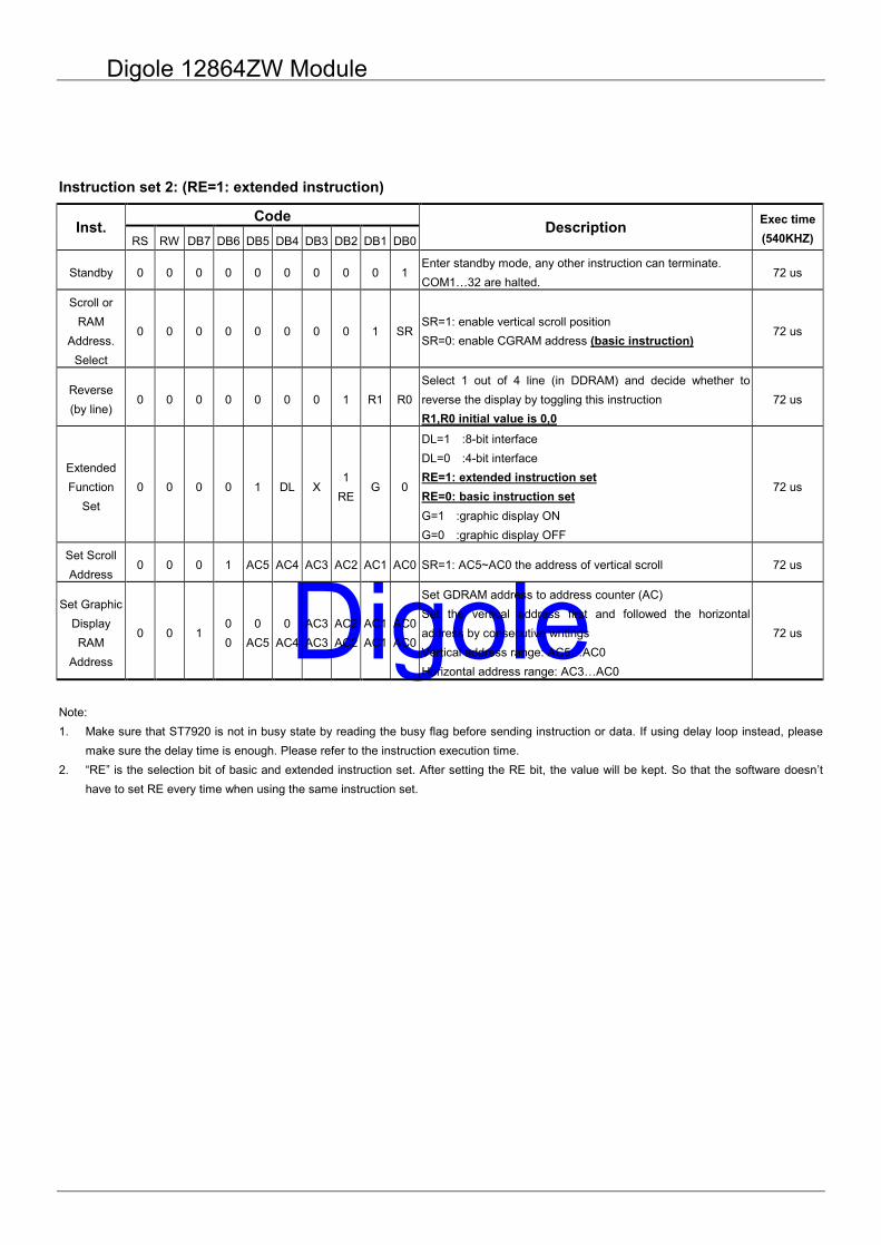
Instruction set 2: (RE=1: extended instruction)
Code Inst.
RS RW DB7 DB6 DB5 DB4 DB3 DB2 DB1 DB0 Description Exec time
(540KHZ)
Standby 0 0 0 0 0 0 0 0 0 1 Enter standby mode, any other instruction can terminate. COM1…32 are halted.
72 us
Scroll or RAM
Address. Select
0 0 0 0 0 0 0 0 1 SR SR=1: enable vertical scroll position SR=0: enable CGRAM address (basic instruction)
72 us
Reverse (by line)
0 0 0 0 0 0 0 1 R1 R0 Select 1 out of 4 line (in DDRAM) and decide whether to reverse the display by toggling this instruction R1,R0 initial value is 0,0
72 us
Extended Function
Set 0 0 0 0 1 DL X
1 RE
G 0
DL=1 :8-bit interface DL=0 :4-bit interface RE=1: extended instruction set RE=0: basic instruction set G=1 :graphic display ON G=0 :graphic display OFF
72 us
Set Scroll Address
0 0 0 1 AC5 AC4 AC3 AC2 AC1 AC0 SR=1: AC5~AC0 the address of vertical scroll 72 us
Set Graphic Display RAM
Address
0 0 1 0 0
0 AC5
0 AC4
AC3 AC3
AC2 AC2
AC1 AC1
AC0 AC0
Set GDRAM address to address counter (AC) Set the vertical address first and followed the horizontal address by consecutive writings Vertical address range: AC5…AC0 Horizontal address range: AC3…AC0
72 us
Note: 1. Make sure that ST7920 is not in busy state by reading the busy flag before sending instruction or data. If using delay loop instead, please
make sure the delay time is enough. Please refer to the instruction execution time. 2. “RE” is the selection bit of basic and extended instruction set. After setting the RE bit, the value will be kept. So that the software doesn’t
have to set RE every time when using the same instruction set.
Digole 12864ZW Module
Digole
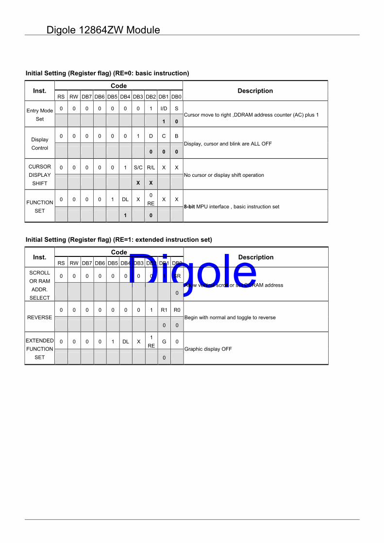
Initial Setting (Register flag) (RE=0: basic instruction)
Code Inst.
RS RW DB7 DB6 DB5 DB4 DB3 DB2 DB1 DB0 Description
0 0 0 0 0 0 0 1 I/D S Entry Mode Set 1 0
Cursor move to right ,DDRAM address counter (AC) plus 1
0 0 0 0 0 0 1 D C B Display Control
0 0 0 Display, cursor and blink are ALL OFF
0 0 0 0 0 1 S/C R/L X X CURSOR DISPLAY
SHIFT X X No cursor or display shift operation
0 0 0 0 1 DL X 0
RE X X FUNCTION
SET 1 0
8-bit MPU interface , basic instruction set
Initial Setting (Register flag) (RE=1: extended instruction set)
Code Inst.
RS RW DB7 DB6 DB5 DB4 DB3 DB2 DB1 DB0 Description
0 0 0 0 0 0 0 0 1 SR SCROLL OR RAM ADDR.
SELECT 0
Allow vertical scroll or set CGRAM address
0 0 0 0 0 0 0 1 R1 R0 REVERSE
0 0 Begin with normal and toggle to reverse
0 0 0 0 1 DL X 1
RE G 0 EXTENDED
FUNCTION SET 0
Graphic display OFF
Digole 12864ZW Module
Digole
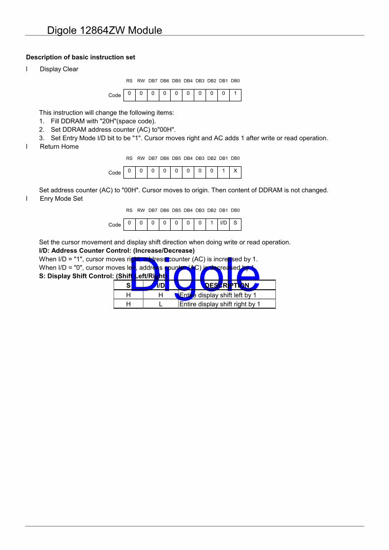
Description of basic instruction set
l Display Clear
This instruction will change the following items: 1. Fill DDRAM with "20H"(space code). 2. Set DDRAM address counter (AC) to"00H". 3. Set Entry Mode I/D bit to be "1". Cursor moves right and AC adds 1 after write or read operation.
l Return Home
Set address counter (AC) to "00H". Cursor moves to origin. Then content of DDRAM is not changed. l Enry Mode Set
Set the cursor movement and display shift direction when doing write or read operation. I/D: Address Counter Control: (Increase/Decrease) When I/D = "1", cursor moves right, address counter (AC) is increased by 1. When I/D = "0", cursor moves left, address counter (AC) is decreased by 1. S: Display Shift Control: (Shift Left/Right)
S I/D DESCRIPTION H H Entire display shift left by 1 H L Entire display shift right by 1
0
0
0
0
0
0
0
0
0
0
0
0
0
0
0
0
0
0
0
0
0
0
0
1
Code
Code
Code
RS
RS
RS
RW
RW
RW
DB7
DB7
DB7
DB6
DB6
DB6
DB5
DB5
DB5
DB4
DB4
DB4
DB1
DB1
DB1
DB2
DB2
DB2
DB3
DB3
DB3
0
1
I/D
1
X
S
DB0
DB0
DB0
Digole 12864ZW Module
Digole
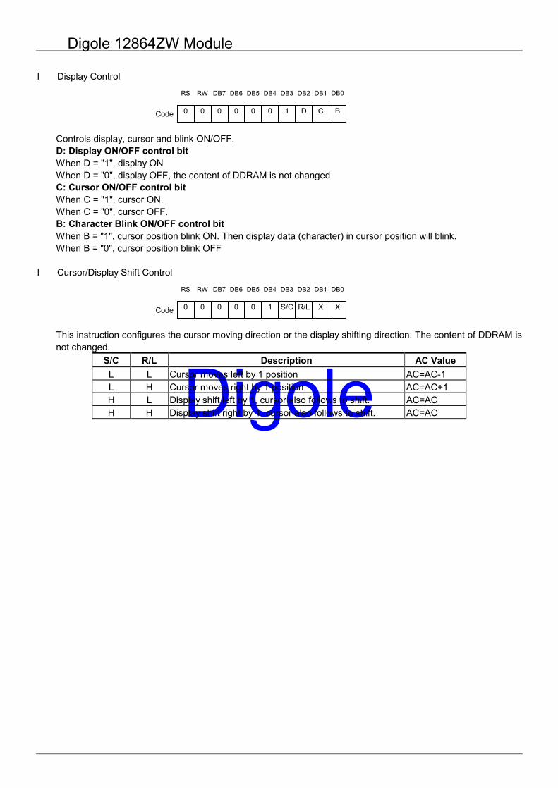
l Display Control
Controls display, cursor and blink ON/OFF. D: Display ON/OFF control bit When D = "1", display ON When D = "0", display OFF, the content of DDRAM is not changed C: Cursor ON/OFF control bit When C = "1", cursor ON. When C = "0", cursor OFF. B: Character Blink ON/OFF control bit When B = "1", cursor position blink ON. Then display data (character) in cursor position will blink. When B = "0", cursor position blink OFF
l Cursor/Display Shift Control
This instruction configures the cursor moving direction or the display shifting direction. The content of DDRAM is not changed.
S/C R/L Description AC Value L L Cursor moves left by 1 position AC=AC-1 L H Cursor moves right by 1 position AC=AC+1 H L Display shift left by 1, cursor also follows to shift. AC=AC H H Display shift right by 1, cursor also follows to shift. AC=AC
0
0
0
0
0
0
0
0
0
0
0
1
1
S/C
D
R/L
Code
Code
RS
RS
RW
RW
DB7
DB7
DB6
DB6
DB5
DB5
DB4
DB4
DB1
DB1
DB2
DB2
DB3
DB3
C
X
B
X
DB0
DB0
Digole 12864ZW Module
Digole
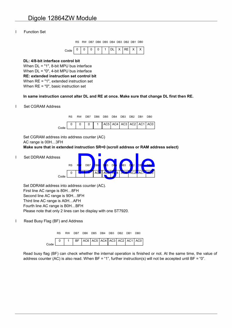
l Function Set
DL: 4/8-bit interface control bit When DL = "1", 8-bit MPU bus interface When DL = "0", 4-bit MPU bus interface RE: extended instruction set control bit When RE = "1", extended instruction set When RE = "0", basic instruction set In same instruction cannot alter DL and RE at once. Make sure that change DL first then RE.
l Set CGRAM Address
Set CGRAM address into address counter (AC) AC range is 00H…3FH Make sure that in extended instruction SR=0 (scroll address or RAM address select)
l Set DDRAM Address
Set DDRAM address into address counter (AC). First line AC range is 80H…8FH Second line AC range is 90H…9FH Third line AC range is A0H…AFH Fourth line AC range is B0H…BFH Please note that only 2 lines can be display with one ST7920.
l Read Busy Flag (BF) and Address
Read busy flag (BF) can check whether the internal operation is finished or not. At the same time, the value of address counter (AC) is also read. When BF = “1”, further instruction(s) will not be accepted until BF = “0”.
0 0 0 0 1 DL X RE Code
RS RW DB7 DB6 DB5 DB4 DB1 DB2 DB3
X X
DB0
0 1 BF AC6 AC5 AC4 AC3 AC2 Code
RS RW DB7 DB6 DB5 DB4 DB1 DB2 DB3
AC1 AC0
DB0
0 0 0 1 AC5 AC4 AC3 AC2 Code
RS RW DB7 DB6 DB5 DB4 DB1 DB2 DB3
AC1 AC0
DB0
0 0 1 AC6 AC5 AC4 AC3 AC2 Code
RS RW DB7 DB6 DB5 DB4 DB1 DB2 DB3
AC1 AC0
DB0
Digole 12864ZW Module
Digole
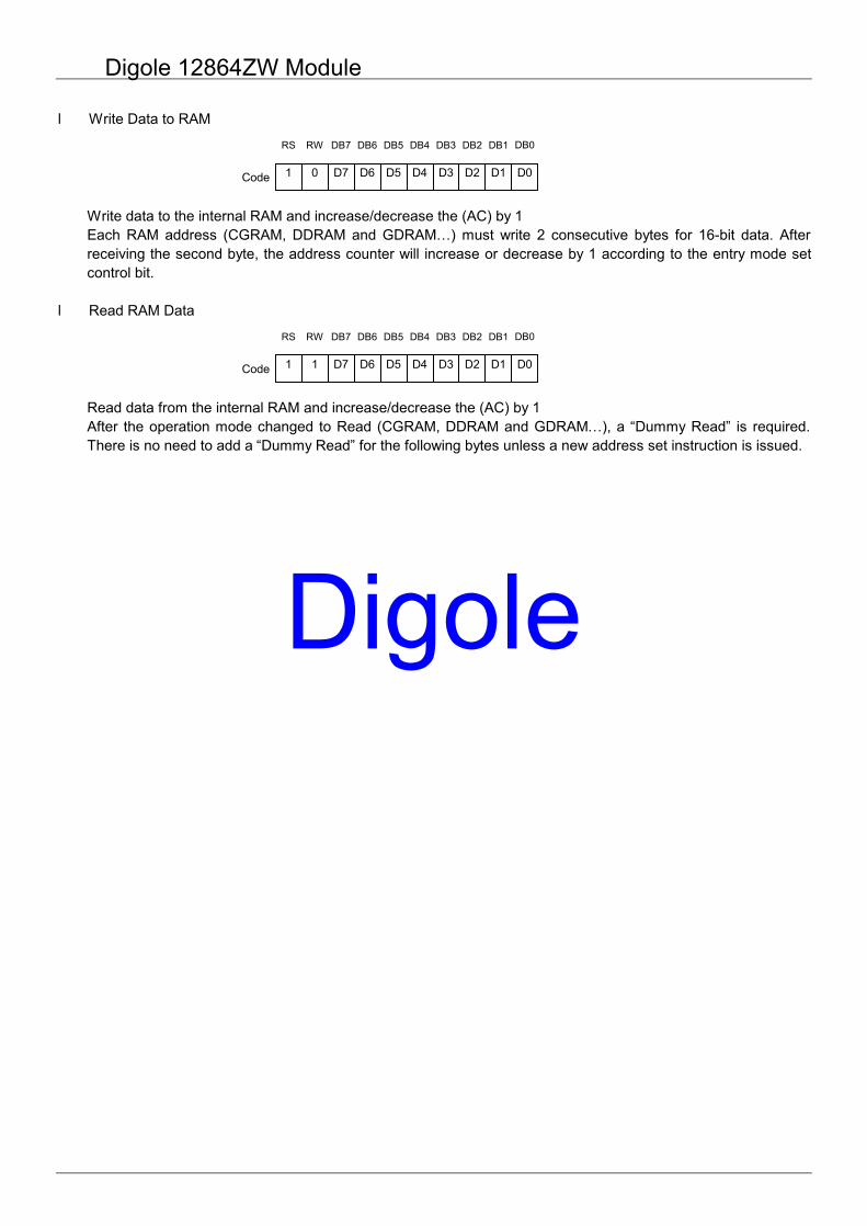
l Write Data to RAM
Write data to the internal RAM and increase/decrease the (AC) by 1 Each RAM address (CGRAM, DDRAM and GDRAM…) must write 2 consecutive bytes for 16-bit data. After receiving the second byte, the address counter will increase or decrease by 1 according to the entry mode set control bit.
l Read RAM Data
Read data from the internal RAM and increase/decrease the (AC) by 1 After the operation mode changed to Read (CGRAM, DDRAM and GDRAM…), a “Dummy Read” is required. There is no need to add a “Dummy Read” for the following bytes unless a new address set instruction is issued.
1
1
0
1
D7
D7
D6
D6
D5
D5
D4
D4
D3
D3
D2
D2
Code
Code
RS
RS
RW
RW
DB7
DB7
DB6
DB6
DB5
DB5
DB4
DB4
DB1
DB1
DB2
DB2
DB3
DB3
D1
D1
D0
D0
DB0
DB0
Digole 12864ZW Module
Digole
Description of extended instruction set
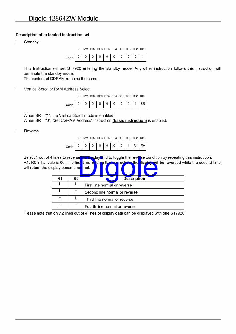
l Standby
This Instruction will set ST7920 entering the standby mode. Any other instruction follows this instruction will terminate the standby mode. The content of DDRAM remains the same.
l Vertical Scroll or RAM Address Select
When SR = "1", the Vertical Scroll mode is enabled. When SR = "0", “Set CGRAM Address” instruction (basic instruction) is enabled.
l Reverse
Select 1 out of 4 lines to reverse the display and to toggle the reverse condition by repeating this instruction. R1, R0 initial vale is 00. The first time issuing this instruction, the display will be reversed while the second time will return the display become normal.
R1 R0 Description L L First line normal or reverse L H Second line normal or reverse H L Third line normal or reverse H H Fourth line normal or reverse
Please note that only 2 lines out of 4 lines of display data can be displayed with one ST7920.
0
0
0
0
0
0
0
0
0
0
0
0
0
0
0
0
0
0
0
0
0
0
0
1
Code
Code
Code
RS
RS
RS
RW
RW
RW
DB7
DB7
DB7
DB6
DB6
DB6
DB5
DB5
DB5
DB4
DB4
DB4
DB1
DB1
DB1
DB2
DB2
DB2
DB3
DB3
DB3
0
1
R1
1
SR
R0
DB0
DB0
DB0
Digole 12864ZW Module
Digole
l Extended Function Set
DL: 4/8-bit interface control bit When DL = "1", 8-bit MPU interface. When DL = "0", 4-bit MPU interface. RE: extended instruction set control bit When RE = "1", extended instruction set When RE = "0", basic instruction set G: Graphic display control bit When G = "1", Graphic Display ON When G = "0", Graphic Display OFF In same instruction cannot alter DL, RE and G at once. Make sure that change DL or G first and then RE.
l Set Scroll Address
SR=1: AC5~AC0 is vertical scroll displacement address
l Set Graphic RAM Address
Set GDRAM address into address counter (AC). This is a 2-byte instruction. The first instruction sets the vertical address while the second one sets the horizontal address (write 2 consecutive bytes to complete the vertical and horizontal address setting). Vertical address range is AC5...AC0 Horizontal address range is AC3…AC0 The address counter (AC) of graphic RAM (GRAM) will be increased automatically after the vertical and horizontal addresses are set. After horizontal address is increased upto 0FH, it will automatically return to 00H. However, the vertical address will not increase as the result of the same action.
0 0 0 0 1 DL X RE Code
RS RW DB7 DB6 DB5 DB4 DB1 DB2 DB3
G X
DB0
0 0 0 1 AC5 AC4 AC3 AC2 Code
RS RW DB7 DB6 DB5 DB4 DB1 DB2 DB3
AC1 AC0
DB0
0 0 1 0 0 0 AC3 AC2 Code
RS RW DB7 DB6 DB5 DB4 DB1 DB2 DB3
AC1 AC0
DB0
0 0 1 0 AC5 AC4 AC3 AC2 Code
RS RW DB7 DB6 DB5 DB4 DB1 DB2 DB3
AC1 AC0
DB0
Digole 12864ZW Module
Digole
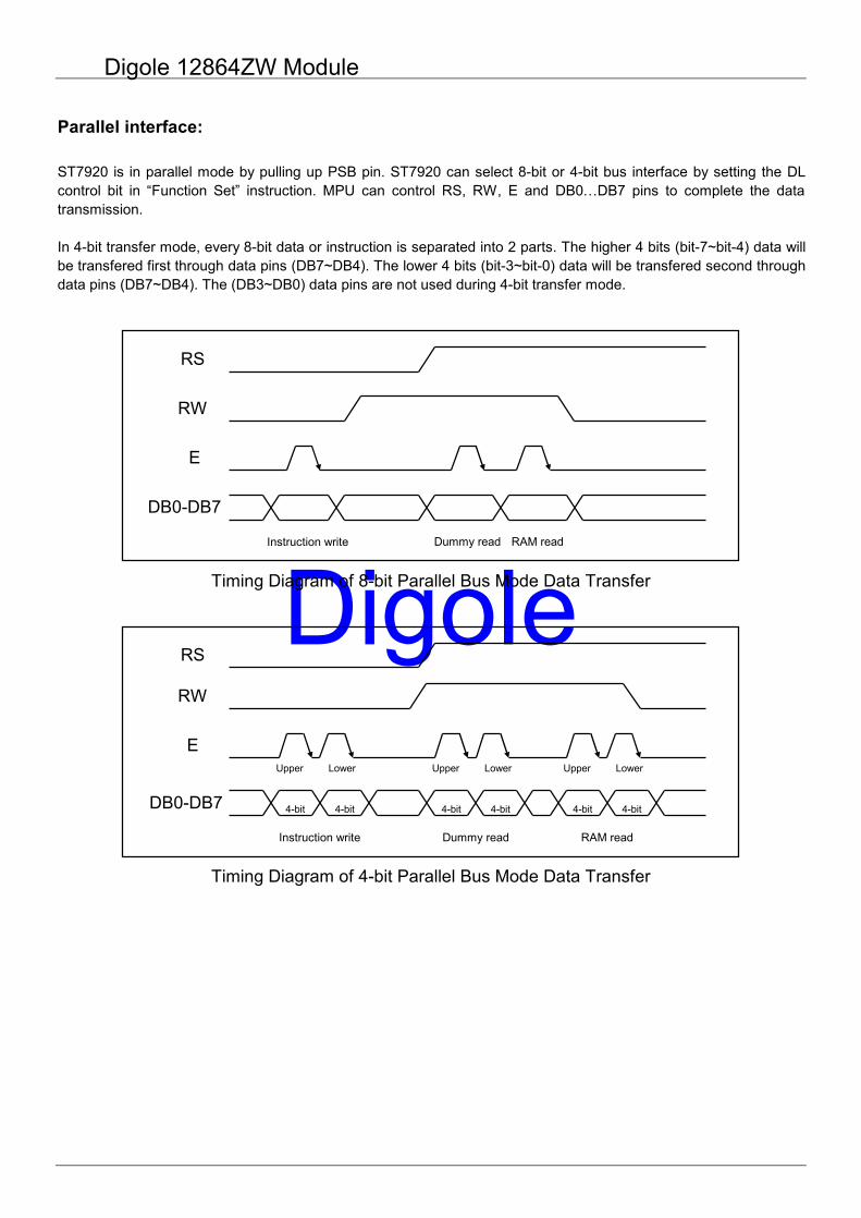
Parallel interface: ST7920 is in parallel mode by pulling up PSB pin. ST7920 can select 8-bit or 4-bit bus interface by setting the DL control bit in “Function Set” instruction. MPU can control RS, RW, E and DB0…DB7 pins to complete the data transmission. In 4-bit transfer mode, every 8-bit data or instruction is separated into 2 parts. The higher 4 bits (bit-7~bit-4) data will be transfered first through data pins (DB7~DB4). The lower 4 bits (bit-3~bit-0) data will be transfered second through data pins (DB7~DB4). The (DB3~DB0) data pins are not used during 4-bit transfer mode.
Timing Diagram of 8-bit Parallel Bus Mode Data Transfer
RS
RW
E
DB0-DB7
Dummy read Instruction write RAM read
Timing Diagram of 4-bit Parallel Bus Mode Data Transfer
RS
RW
E Upper Lower Upper Lower Upper Lower
DB0-DB7
Dummy read Instruction write RAM read
4-bit 4-bit 4-bit 4-bit 4-bit 4-bit
Digole 12864ZW Module
Digole
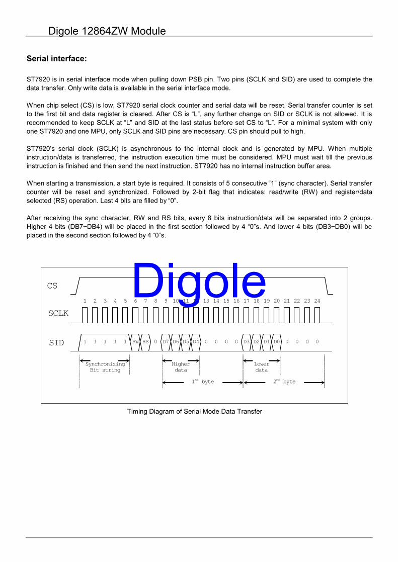
Serial interface: ST7920 is in serial interface mode when pulling down PSB pin. Two pins (SCLK and SID) are used to complete the data transfer. Only write data is available in the serial interface mode. When chip select (CS) is low, ST7920 serial clock counter and serial data will be reset. Serial transfer counter is set to the first bit and data register is cleared. After CS is “L”, any further change on SID or SCLK is not allowed. It is recommended to keep SCLK at “L” and SID at the last status before set CS to “L”. For a minimal system with only one ST7920 and one MPU, only SCLK and SID pins are necessary. CS pin should pull to high. ST7920’s serial clock (SCLK) is asynchronous to the internal clock and is generated by MPU. When multiple instruction/data is transferred, the instruction execution time must be considered. MPU must wait till the previous instruction is finished and then send the next instruction. ST7920 has no internal instruction buffer area. When starting a transmission, a start byte is required. It consists of 5 consecutive “1” (sync character). Serial transfer counter will be reset and synchronized. Followed by 2-bit flag that indicates: read/write (RW) and register/data selected (RS) operation. Last 4 bits are filled by “0”. After receiving the sync character, RW and RS bits, every 8 bits instruction/data will be separated into 2 groups. Higher 4 bits (DB7~DB4) will be placed in the first section followed by 4 “0”s. And lower 4 bits (DB3~DB0) will be placed in the second section followed by 4 “0”s.
1 2 4 5 6 7 8 9 10 11 12 13 14 15 16 17 18 19 20 21 22 23 24
1 1 1 1 1 RW RS 0 D7 D6 D5 D4 0 0 0 0 0 0 0 0 D3 D2 D1 D0
CS
SCLK
SID
Synchronizing Bit string
Higher data
Lower data
3
1st byte 2nd byte
Timing Diagram of Serial Mode Data Transfer
Digole 12864ZW Module
Digole
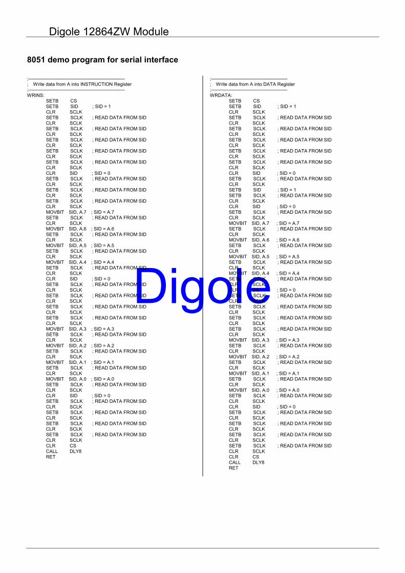
8051 demo program for serial interface ;-------------------------------------------------------------- ; Write data from A into INSTRUCTION Register ;-------------------------------------------------------------- WRINS: SETB CS SETB SID ; SID = 1 CLR SCLK SETB SCLK ; READ DATA FROM SID CLR SCLK SETB SCLK ; READ DATA FROM SID CLR SCLK SETB SCLK ; READ DATA FROM SID CLR SCLK SETB SCLK ; READ DATA FROM SID CLR SCLK SETB SCLK ; READ DATA FROM SID CLR SCLK CLR SID ; SID = 0 SETB SCLK ; READ DATA FROM SID CLR SCLK SETB SCLK ; READ DATA FROM SID CLR SCLK SETB SCLK ; READ DATA FROM SID CLR SCLK MOVBIT SID, A.7 ; SID = A.7 SETB SCLK ; READ DATA FROM SID CLR SCLK MOVBIT SID, A.6 ; SID = A.6 SETB SCLK ; READ DATA FROM SID CLR SCLK MOVBIT SID, A.5 ; SID = A.5 SETB SCLK ; READ DATA FROM SID CLR SCLK MOVBIT SID, A.4 ; SID = A.4 SETB SCLK ; READ DATA FROM SID CLR SCLK CLR SID ; SID = 0 SETB SCLK ; READ DATA FROM SID CLR SCLK SETB SCLK ; READ DATA FROM SID CLR SCLK SETB SCLK ; READ DATA FROM SID CLR SCLK SETB SCLK ; READ DATA FROM SID CLR SCLK MOVBIT SID, A.3 ; SID = A.3 SETB SCLK ; READ DATA FROM SID CLR SCLK MOVBIT SID, A.2 ; SID = A.2 SETB SCLK ; READ DATA FROM SID CLR SCLK MOVBIT SID, A.1 ; SID = A.1 SETB SCLK ; READ DATA FROM SID CLR SCLK MOVBIT SID, A.0 ; SID = A.0 SETB SCLK ; READ DATA FROM SID CLR SCLK CLR SID ; SID = 0 SETB SCLK ; READ DATA FROM SID CLR SCLK SETB SCLK ; READ DATA FROM SID CLR SCLK SETB SCLK ; READ DATA FROM SID CLR SCLK SETB SCLK ; READ DATA FROM SID CLR SCLK CLR CS CALL DLY8 RET
;------------------------------------------------- ; Write data from A into DATA Register ;------------------------------------------------- WRDATA: SETB CS SETB SID ; SID = 1 CLR SCLK SETB SCLK ; READ DATA FROM SID CLR SCLK SETB SCLK ; READ DATA FROM SID CLR SCLK SETB SCLK ; READ DATA FROM SID CLR SCLK SETB SCLK ; READ DATA FROM SID CLR SCLK SETB SCLK ; READ DATA FROM SID CLR SCLK CLR SID ; SID = 0 SETB SCLK ; READ DATA FROM SID CLR SCLK SETB SID ; SID = 1 SETB SCLK ; READ DATA FROM SID CLR SCLK CLR SID ; SID = 0 SETB SCLK ; READ DATA FROM SID CLR SCLK MOVBIT SID, A.7 ; SID = A.7 SETB SCLK ; READ DATA FROM SID CLR SCLK MOVBIT SID, A.6 ; SID = A.6 SETB SCLK ; READ DATA FROM SID CLR SCLK MOVBIT SID, A.5 ; SID = A.5 SETB SCLK ; READ DATA FROM SID CLR SCLK MOVBIT SID, A.4 ; SID = A.4 SETB SCLK ; READ DATA FROM SID CLR SCLK CLR SID ; SID = 0 SETB SCLK ; READ DATA FROM SID CLR SCLK SETB SCLK ; READ DATA FROM SID CLR SCLK SETB SCLK ; READ DATA FROM SID CLR SCLK SETB SCLK ; READ DATA FROM SID CLR SCLK MOVBIT SID, A.3 ; SID = A.3 SETB SCLK ; READ DATA FROM SID CLR SCLK MOVBIT SID, A.2 ; SID = A.2 SETB SCLK ; READ DATA FROM SID CLR SCLK MOVBIT SID, A.1 ; SID = A.1 SETB SCLK ; READ DATA FROM SID CLR SCLK MOVBIT SID, A.0 ; SID = A.0 SETB SCLK ; READ DATA FROM SID CLR SCLK CLR SID ; SID = 0 SETB SCLK ; READ DATA FROM SID CLR SCLK SETB SCLK ; READ DATA FROM SID CLR SCLK SETB SCLK ; READ DATA FROM SID CLR SCLK SETB SCLK ; READ DATA FROM SID CLR SCLK CLR CS CALL DLY8 RET
Digole 12864ZW Module
Digole
Application circuit for testing CGROM and HCGROM:
We can use the function of “CHECK SUM” to check the CGROM is right or error. See the following notes: Useing IC Pad (Pin4àCLK, Pin5àTT1, Pin6àTT2) to do the “CHECK SUM” function. The application circuit is at Page49.
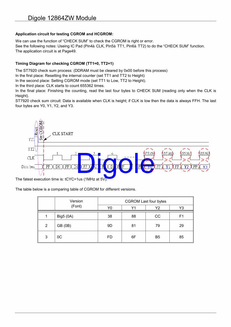
Timing Diagram for checking CGROM (TT1=0, TT2=1)
The ST7920 check sum process: (DDRAM must be cleared by 0x00 before this process) In the first place: Resetting the internal counter (set TT1 and TT2 to Height) In the second place: Setting CGROM mode (set TT1 to Low, TT2 to Height). In the third place: CLK starts to count 655362 times. In the final place: Finishing the counting, read the last four bytes to CHECK SUM (reading only when the CLK is Height). ST7920 check sum circuit: Data is available when CLK is height; if CLK is low then the data is always FFH. The last four bytes are Y0, Y1, Y2, and Y3.
The fatest execution time is: tCYC=1us (1MHz at 5V). The table below is a comparing table of CGROM for different versions.
CGROM Last four bytes Version (Font) Y0 Y1 Y2 Y3
1 Big5 (0A) 38 88 CC F1
2 GB (0B) 9D 81 79 29
3 0C FD 6F B5 85
Digole 12864ZW Module
Digole
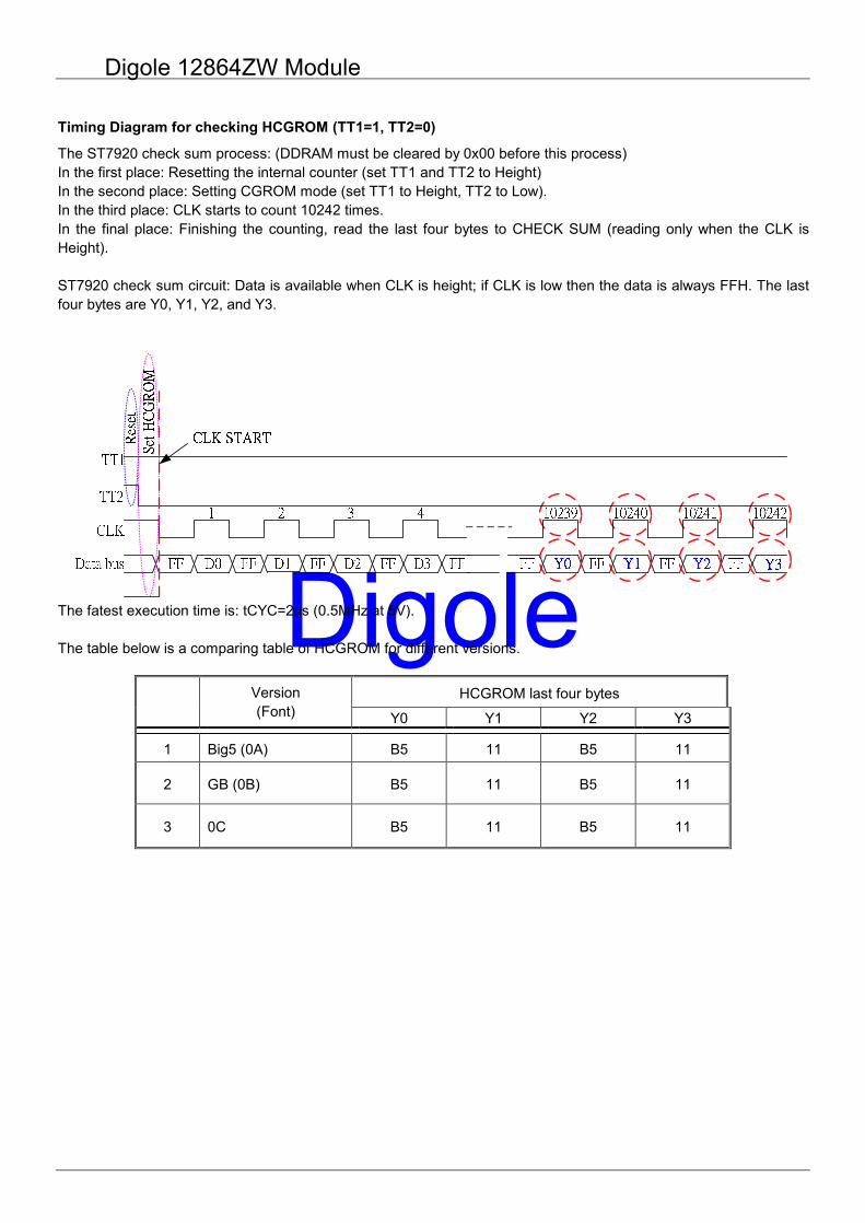
Timing Diagram for checking HCGROM (TT1=1, TT2=0)
The ST7920 check sum process: (DDRAM must be cleared by 0x00 before this process) In the first place: Resetting the internal counter (set TT1 and TT2 to Height) In the second place: Setting CGROM mode (set TT1 to Height, TT2 to Low). In the third place: CLK starts to count 10242 times. In the final place: Finishing the counting, read the last four bytes to CHECK SUM (reading only when the CLK is Height). ST7920 check sum circuit: Data is available when CLK is height; if CLK is low then the data is always FFH. The last four bytes are Y0, Y1, Y2, and Y3.
The fatest execution time is: tCYC=2us (0.5MHz at 5V). The table below is a comparing table of HCGROM for different versions.
HCGROM last four bytes Version (Font) Y0 Y1 Y2 Y3
1 Big5 (0A) B5 11 B5 11
2 GB (0B) B5 11 B5 11
3 0C B5 11 B5 11
Digole 12864ZW Module
Digole
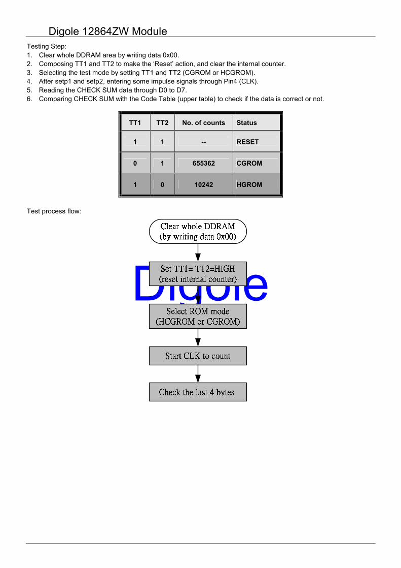
Testing Step: 1. Clear whole DDRAM area by writing data 0x00. 2. Composing TT1 and TT2 to make the ‘Reset’ action, and clear the internal counter. 3. Selecting the test mode by setting TT1 and TT2 (CGROM or HCGROM). 4. After setp1 and setp2, entering some impulse signals through Pin4 (CLK). 5. Reading the CHECK SUM data through D0 to D7. 6. Comparing CHECK SUM with the Code Table (upper table) to check if the data is correct or not.
TT1 TT2 No. of counts Status
1 1 -- RESET
0 1 655362 CGROM
1 0 10242 HGROM
Test process flow:
Digole 12864ZW Module
Digole
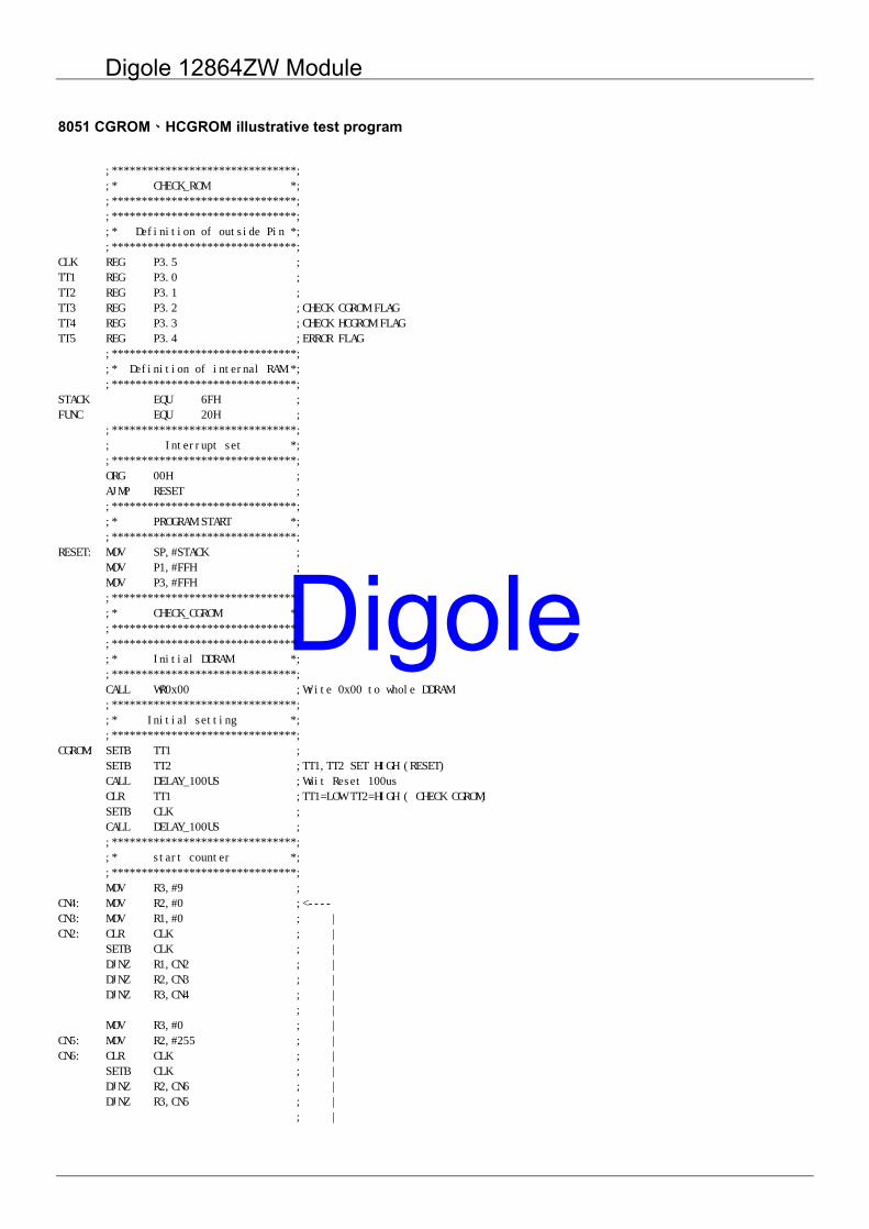
8051 CGROM、HCGROM illustrative test program
;*******************************;
;* CHECK_ROM *;
;*******************************;
;*******************************;
;* Definition of outside Pin *;
;*******************************;
CLK REG P3.5 ;
TT1 REG P3.0 ;
TT2 REG P3.1 ;
TT3 REG P3.2 ;CHECK CGROM FLAG
TT4 REG P3.3 ;CHECK HCGROM FLAG
TT5 REG P3.4 ;ERROR FLAG
;*******************************;
;* Definition of internal RAM *;
;*******************************;
STACK EQU 6FH ;
FUNC EQU 20H ;
;*******************************;
; Interrupt set *;
;*******************************;
ORG 00H ;
AJMP RESET ;
;*******************************;
;* PROGRAM START *;
;*******************************;
RESET: MOV SP,#STACK ;
MOV P1,#FFH ;
MOV P3,#FFH ;
;*******************************;
;* CHECK_CGROM *;
;*******************************;
;*******************************;
;* Initial DDRAM *;
;*******************************;
CALL WR0x00 ;Write 0x00 to whole DDRAM
;*******************************;
;* Initial setting *;
;*******************************;
CGROM: SETB TT1 ;
SETB TT2 ;TT1,TT2 SET HIGH (RESET)
CALL DELAY_100US ;Wait Reset 100us
CLR TT1 ;TT1=LOW TT2=HIGH ( CHECK CGROM)
SETB CLK ;
CALL DELAY_100US ;
;*******************************;
;* start counter *;
;*******************************;
MOV R3,#9 ;
CN4: MOV R2,#0 ;<----
CN3: MOV R1,#0 ; |
CN2: CLR CLK ; |
SETB CLK ; |
DJNZ R1,CN2 ; |
DJNZ R2,CN3 ; |
DJNZ R3,CN4 ; |
; |
MOV R3,#0 ; |
CN5: MOV R2,#255 ; |
CN6: CLR CLK ; |
SETB CLK ; |
DJNZ R2,CN6 ; |
DJNZ R3,CN5 ; |
; |
Digole 12864ZW Module
Digole
MOV R3,#63 ; |
CN7: MOV R2,#2 ; |
CN8: MOV R1,#2 ; |
CN9: CLR CLK ; |
SETB CLK ; |
DJNZ R1,CN9 ; |
DJNZ R2,CN8 ; |
DJNZ R3,CN7 ; |
CLR CLK ; |
SETB CLK ; |
CLR CLK ; |
SETB CLK ;<---- Counter 655356
;-------------------------------;
CLR CLK ;Counter 655357
SETB CLK ;
MOV A,P1 ;A=Y0
CJNE A,#FDH,ERRORC ;COMPARE Y0 DATA
CLR CLK ;Counter 655358
SETB CLK ;
MOV A,P1 ;A=Y1
CJNE A,#6FH,ERRORC ;COMPARE Y1 DATA
CLR CLK ;Counter 655359
SETB CLK ;
MOV A,P1 ;A=Y2
CJNE A,#B5H,ERRORC ;COMPARE Y2 DATA
CLR CLK ;Counter 655360
SETB CLK ;
MOV A,P1 ;A=Y3
CJNE A,#85H,ERRORC ;COMPARE Y3 DATA
CLR CLK ;
CLR TT3 ;IF OK CLR TT3
CALL HCGROM ;
ERRORC: ;
CLR TT5 ;IF CGROM CHECK ERROR CLR TT5
;---------------------------------------;
;*******************************;
;* CHECK_HCGROM *;
;*******************************;
;*******************************;
;* Initial setting *;
;*******************************;
HCGROM: SETB TT1 ;
SETB TT2 ;TT1,TT2 SET HIGH (RESET)
CALL DELAY_100US ;Wait Reset 100us
CLR TT2 ;TT2=LOW TT1=HIGH ( CHECK HCGROM)
SETB CLK ;
CALL DELAY_100US ;
;*******************************;
;* start counter *;
;*******************************;
MOV R3,#9 ;
N4: MOV R2,#32 ;<----
N3: MOV R1,#32 ; |
N2: CLR CLK ; |
SETB CLK ; |
DJNZ R1,N2 ; |
DJNZ R2,N3 ; |
DJNZ R3,N4 ; |
; |
MOV R3,#32 ; |
N5: MOV R2,#31 ; |
N6: CLR CLK ; |
SETB CLK ; |
DJNZ R2,N6 ; |
DJNZ R3,N5 ; |
; |
MOV R2,#30 ; |
Digole 12864ZW Module
Digole
N7: CLR CLK ; |
SETB CLK ; |
DJNZ R2,N7 ; |
;---------------------------------------;<---- Counter 10236
CLR CLK ;Counter 10237
SETB CLK ;
MOV A,P1 ;A=Y0
CJNE A,#B5H,ERROR ;COMPARE Y0 DATA
CLR CLK ;Counter 10238
SETB CLK ;
MOV A,P1 ;A=Y1
CJNE A,#11H,ERROR ;COMPARE Y1 DATA
CLR CLK ;Counter 10239
SETB CLK ;
MOV A,P1 ;A=Y2
CJNE A,#B5H,ERROR ;COMPARE Y2 DATA
CLR CLK ;Counter 10240
SETB CLK ;
MOV A,P1 ;A=Y3
CJNE A,#11H,ERROR ;COMPARE Y3 DATA
CLR CLK ;
CLR TT4 ;IF HCGROM CHECK OK THEN CLR TT4
AJMP $ ;
ERROR: ;
CLR TT5 ;IF HCGROM CHECK ERROR THEN CLR TT5
AJMP $ ;
;*******************************;
;* DELAY TIME 100US *;
;*******************************;
DELAY_100US ;
DEL_10 MOV R6,#5 ;
DEL_9 MOV R7,#3 ;
DJNZ R7,$ ;
DJNZ R6,DEL_9 ;
RET ;
END ;
Digole 12864ZW Module
Digole
8-bit interface:
POWER ON
Wait time >40ms
XRESET LOW HIGH
Function set
RS RW DB7 DB6 DB5 DB4 DB3 DB2 DB1 DB0
0 0 0 0 1 1 X 0 X X
Wait time >100uS
Function set
RS RW DB7 DB6 DB5 DB4 DB3 DB2 DB1 DB0
0 0 0 0 1 1 X 0 X X
Wait time >37uS
Display ON/OFF control
RS RW DB7 DB6 DB5 DB4 DB3 DB2 DB1 DB0
0 0 0 0 0 0 1 D C B
Wait time >100uS
Display clear
RS RW DB7 DB6 DB5 DB4 DB3 DB2 DB1 DB0
0 0 0 0 0 0 0 0 0 1
Wait time >10mS
Entry mode set
RS RW DB7 DB6 DB5 DB4 DB3 DB2 DB1 DB0
0 0 0 0 0 0 0 1 I/D S
Initialization end
Digole 12864ZW Module
Digole
4-bit interface:
POWER ON
Wait time > 40mS(for VDD stable)
XRESET: LOW HIGH
Wait time > 100μS
Wait time > 100μS
Display ON/OFF ControlRS R/W DB7 DB6 DB5 DB4 DB3 DB2 DB1 DB0
Wait time > 100μS
INITIALIZATION END
Function setRS R/W DB7 DB6 DB5 DB4 DB3 DB2 DB1 DB0
Function setRS R/W DB7 DB6 DB5 DB4 DB3 DB2 DB1 DB00 0 0 0 1 0 X X X X0 0 X 0 X X X X X X
0 0 0 0 1 0 X X X X0 0 X 0 X X X X X X
X X X XX X X X
0 0 0 0 0 00 0 1 D C B
Display ClearRS R/W DB7 DB6 DB5 DB4 DB3 DB2 DB1 DB0
Wait time > 10mS
X X X XX X X X
0 0 0 0 0 00 0 0 0 0 1
Entry Mode SetRS R/W DB7 DB6 DB5 DB4 DB3 DB2 DB1 DB0
X X X XX X X X
0 0 0 0 0 00 0 0 1 I/D S
Digole 12864ZW Module
Digole
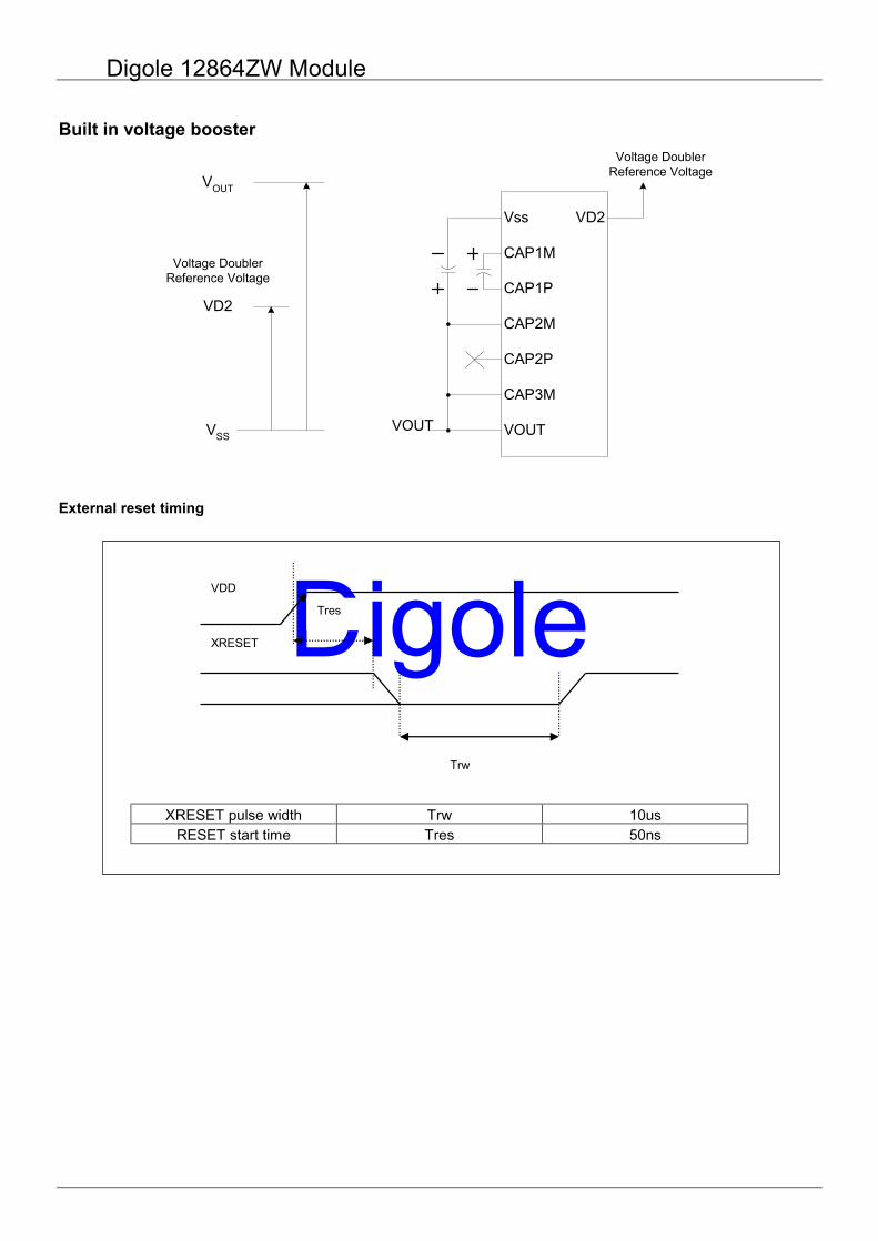
Built in voltage booster
VSS
VD2
Voltage DoublerReference Voltage
VOUT
Vss
CAP1M
Voltage DoublerReference Voltage
CAP1P
CAP2M
CAP2P
CAP3M
VOUT
VD2
VOUT
External reset timing
XRESET pulse width Trw 10us RESET start time Tres 50ns
Tres
Trw
VDD
XRESET
Digole 12864ZW Module
Digole
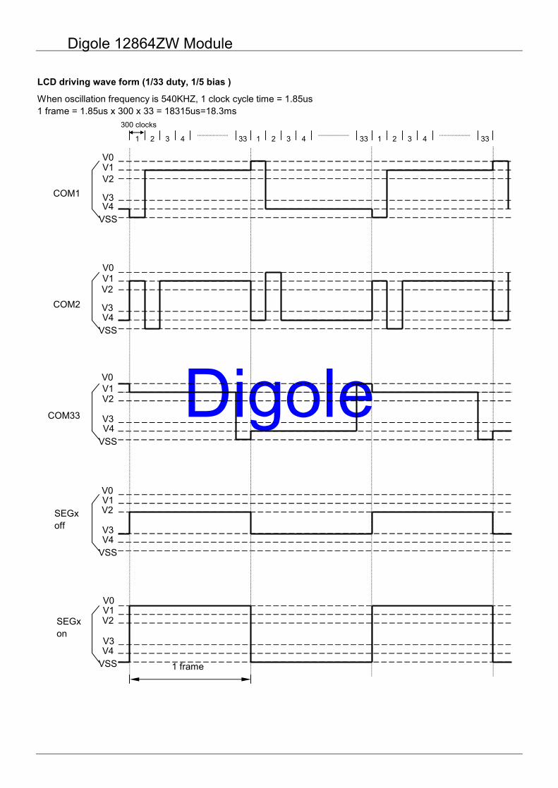
LCD driving wave form (1/33 duty, 1/5 bias )
When oscillation frequency is 540KHZ, 1 clock cycle time = 1.85us 1 frame = 1.85us x 300 x 33 = 18315us=18.3ms 1 2 3 4 33 1 2 3 4 33 1 2 3 4 33
V0 V1 V2
V3 V4
VSS
COM1
V0 V1 V2
V3 V4
VSS
COM2
V0 V1 V2
V3 V4
VSS
COM33
V0 V1 V2
V3 V4
VSS
SEGx off
V0 V1 V2
V3 V4
VSS
SEGx on
1 frame
300 clocks
Digole 12864ZW Module
Digole
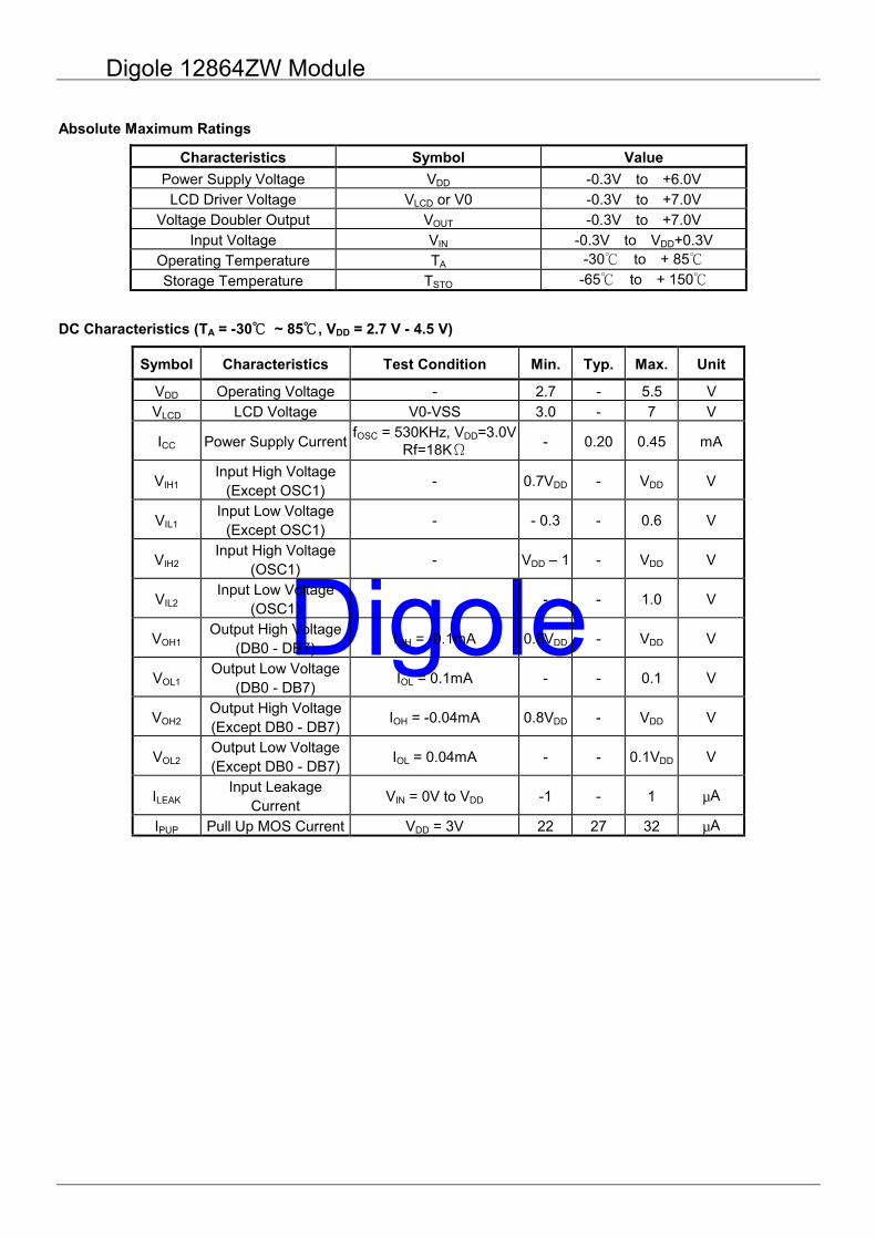
Absolute Maximum Ratings
Characteristics Symbol Value Power Supply Voltage VDD -0.3V to +6.0V
LCD Driver Voltage VLCD or V0 -0.3V to +7.0V Voltage Doubler Output VOUT -0.3V to +7.0V
Input Voltage VIN -0.3V to VDD+0.3V Operating Temperature TA -30 to + 85 Storage Temperature TSTO -65 to + 150
DC Characteristics (TA = -30 ~ 85, VDD = 2.7 V - 4.5 V)
Symbol Characteristics Test Condition Min. Typ. Max. Unit
VDD Operating Voltage - 2.7 - 5.5 V VLCD LCD Voltage V0-VSS 3.0 - 7 V
ICC Power Supply Current fOSC = 530KHz, VDD=3.0V Rf=18KΩ - 0.20 0.45 mA
VIH1 Input High Voltage
(Except OSC1) - 0.7VDD - VDD V
VIL1 Input Low Voltage
(Except OSC1) - - 0.3 - 0.6 V
VIH2 Input High Voltage
(OSC1) - VDD – 1 - VDD V
VIL2 Input Low Voltage
(OSC1) - - - 1.0 V
VOH1 Output High Voltage
(DB0 - DB7) IOH = -0.1mA 0.8VDD - VDD V
VOL1 Output Low Voltage
(DB0 - DB7) IOL = 0.1mA - - 0.1 V
VOH2 Output High Voltage (Except DB0 - DB7) IOH = -0.04mA 0.8VDD - VDD V
VOL2 Output Low Voltage (Except DB0 - DB7) IOL = 0.04mA - - 0.1VDD V
ILEAK Input Leakage Current VIN = 0V to VDD -1 - 1 µA
IPUP Pull Up MOS Current VDD = 3V 22 27 32 µA
Digole 12864ZW Module
Digole
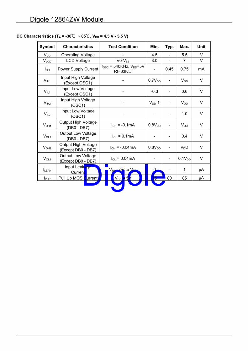
DC Characteristics (TA = -30 ~ 85, VDD = 4.5 V - 5.5 V)
Symbol Characteristics Test Condition Min. Typ. Max. Unit
VDD Operating Voltage - 4.5 - 5.5 V VLCD LCD Voltage V0-VSS 3.0 - 7 V
ICC Power Supply Current fOSC = 540KHz, VDD=5V Rf=33KΩ - 0.45 0.75 mA
VIH1 Input High Voltage
(Except OSC1) - 0.7VDD - VDD V
VIL1 Input Low Voltage
(Except OSC1) - -0.3 - 0.6 V
VIH2 Input High Voltage
(OSC1) - VDD-1 - VDD V
VIL2 Input Low Voltage
(OSC1) - - - 1.0 V
VOH1 Output High Voltage
(DB0 - DB7) IOH = -0.1mA 0.8VDD - VDD V
VOL1 Output Low Voltage
(DB0 - DB7) IOL = 0.1mA - - 0.4 V
VOH2 Output High Voltage (Except DB0 - DB7) IOH = -0.04mA 0.8VDD - VDD V
VOL2 Output Low Voltage (Except DB0 - DB7) IOL = 0.04mA - - 0.1VDD V
ILEAK Input Leakage Current VIN = 0V to VDD -1 - 1 µA
IPUP Pull Up MOS Current VDD = 5V 75 80 85 µA
Digole 12864ZW Module

Digole
AC Characteristics (TA = -30 ~ 85, VDD = 4.5V) Parallel Mode Interface
Symbol Characteristics Test Condition Min. Typ. Max. Unit Internal Clock Operation
fOSC OSC Frequency R = 33KΩ 480 540 600 KHz External Clock Operation
fEX External Frequency - 480 540 600 KHz Duty Cycle - 45 50 55 %
TR,TF Rise/Fall Time - - - 0.2 µs Write Mode (Writing data from MPU to ST7920)
TC Enable Cycle Time Pin E 1200 - - ns TPW Enable Pulse Width Pin E 140 - - ns
TR,TF Enable Rise/Fall Time Pin E - - 25 ns TAS Address Setup Time Pins: RS,RW,E 10 - - ns TAH Address Hold Time Pins: RS,RW,E 20 - - ns
TDSW Data Setup Time Pins: DB0 - DB7 40 - - ns TH Data Hold Time Pins: DB0 - DB7 20 - - ns
Read Mode (Reading Data from ST7920 to MPU) TC Enable Cycle Time Pin E 1200 - - ns
TPW Enable Pulse Width Pin E 140 - - ns TR,TF Enable Rise/Fall Time Pin E - - 25 ns TAS Address Setup Time Pins: RS,RW,E 10 - - ns TAH Address Hold Time Pins: RS,RW,E 20 - - ns TDDR Data Delay Time Pins: DB0 - DB7 - - 100 ns TH Data Hold Time Pins: DB0 - DB7 20 - - ns
Interface Mode with LCD Driver(ST7921) TCWH Clock Pulse with High Pins: CL1, CL2 800 - - ns TCWL Clock Pulse with Low Pins: CL1, CL2 800 - - ns TCST Clock Setup Time Pins: CL1, CL2 500 - - ns TSU Data Setup Time Pin: D 300 - - ns TDH Data Hold Time Pin: D 300 - - ns TDM M Delay Time Pin: M -1000 - 1000 ns
Digole 12864ZW Module
Digole
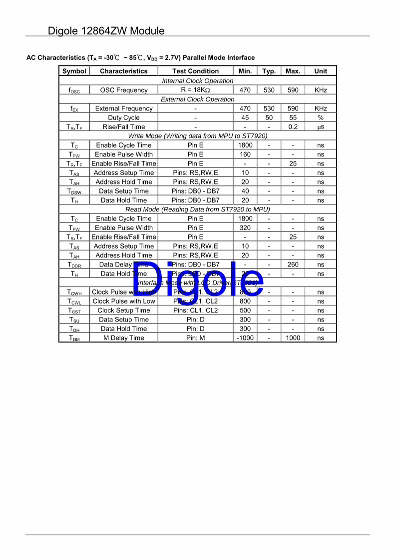
AC Characteristics (TA = -30 ~ 85, VDD = 2.7V) Parallel Mode Interface
Symbol Characteristics Test Condition Min. Typ. Max. Unit Internal Clock Operation
fOSC OSC Frequency R = 18KΩ 470 530 590 KHz External Clock Operation
fEX External Frequency - 470 530 590 KHz Duty Cycle - 45 50 55 %
TR,TF Rise/Fall Time - - - 0.2 µs Write Mode (Writing data from MPU to ST7920)
TC Enable Cycle Time Pin E 1800 - - ns TPW Enable Pulse Width Pin E 160 - - ns
TR,TF Enable Rise/Fall Time Pin E - - 25 ns TAS Address Setup Time Pins: RS,RW,E 10 - - ns TAH Address Hold Time Pins: RS,RW,E 20 - - ns
TDSW Data Setup Time Pins: DB0 - DB7 40 - - ns TH Data Hold Time Pins: DB0 - DB7 20 - - ns
Read Mode (Reading Data from ST7920 to MPU) TC Enable Cycle Time Pin E 1800 - - ns
TPW Enable Pulse Width Pin E 320 - - ns TR,TF Enable Rise/Fall Time Pin E - - 25 ns TAS Address Setup Time Pins: RS,RW,E 10 - - ns TAH Address Hold Time Pins: RS,RW,E 20 - - ns TDDR Data Delay Time Pins: DB0 - DB7 - - 260 ns TH Data Hold Time Pins: DB0 - DB7 20 - - ns
Interface Mode with LCD Driver(ST7921) TCWH Clock Pulse with High Pins: CL1, CL2 800 - - ns TCWL Clock Pulse with Low Pins: CL1, CL2 800 - - ns TCST Clock Setup Time Pins: CL1, CL2 500 - - ns TSU Data Setup Time Pin: D 300 - - ns TDH Data Hold Time Pin: D 300 - - ns TDM M Delay Time Pin: M -1000 - 1000 ns
Digole 12864ZW Module
Digole
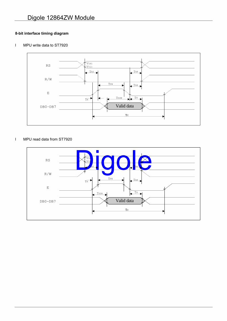
8-bit interface timing diagram
l MPU write data to ST7920 l MPU read data from ST7920
Valid data
RS
R/W
E
DB0-DB7
VIH1VIL1TAS TAH
TAHTPWTR
TDDR TH
TCTC
Valid data
RS
R/W
E
DB0-DB7
VIH1VIL1TAS TAH
TAHTPW
TH
TCTC
TDSWTR
Digole 12864ZW Module
Digole
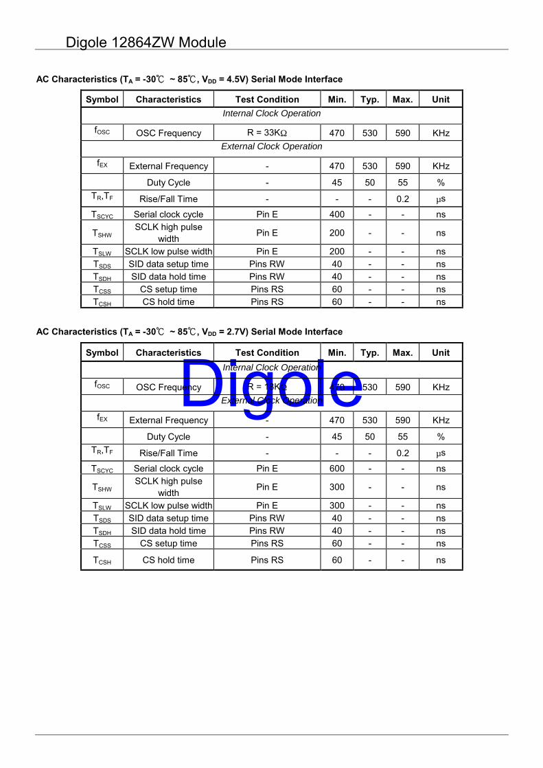
AC Characteristics (TA = -30 ~ 85, VDD = 4.5V) Serial Mode Interface
Symbol Characteristics Test Condition Min. Typ. Max. Unit Internal Clock Operation
fOSC OSC Frequency R = 33KΩ 470 530 590 KHz External Clock Operation
fEX External Frequency - 470 530 590 KHz Duty Cycle - 45 50 55 %
TR,TF Rise/Fall Time - - - 0.2 µs
TSCYC Serial clock cycle Pin E 400 - - ns
TSHW SCLK high pulse width Pin E 200 - - ns
TSLW SCLK low pulse width Pin E 200 - - ns TSDS SID data setup time Pins RW 40 - - ns TSDH SID data hold time Pins RW 40 - - ns TCSS CS setup time Pins RS 60 - - ns TCSH CS hold time Pins RS 60 - - ns
AC Characteristics (TA = -30 ~ 85, VDD = 2.7V) Serial Mode Interface
Symbol Characteristics Test Condition Min. Typ. Max. Unit Internal Clock Operation
fOSC OSC Frequency R = 18KΩ 470 530 590 KHz External Clock Operation
fEX External Frequency - 470 530 590 KHz Duty Cycle - 45 50 55 %
TR,TF Rise/Fall Time - - - 0.2 µs
TSCYC Serial clock cycle Pin E 600 - - ns
TSHW SCLK high pulse width Pin E 300 - - ns
TSLW SCLK low pulse width Pin E 300 - - ns TSDS SID data setup time Pins RW 40 - - ns TSDH SID data hold time Pins RW 40 - - ns TCSS CS setup time Pins RS 60 - - ns
TCSH CS hold time Pins RS 60 - - ns
Digole 12864ZW Module
Digole
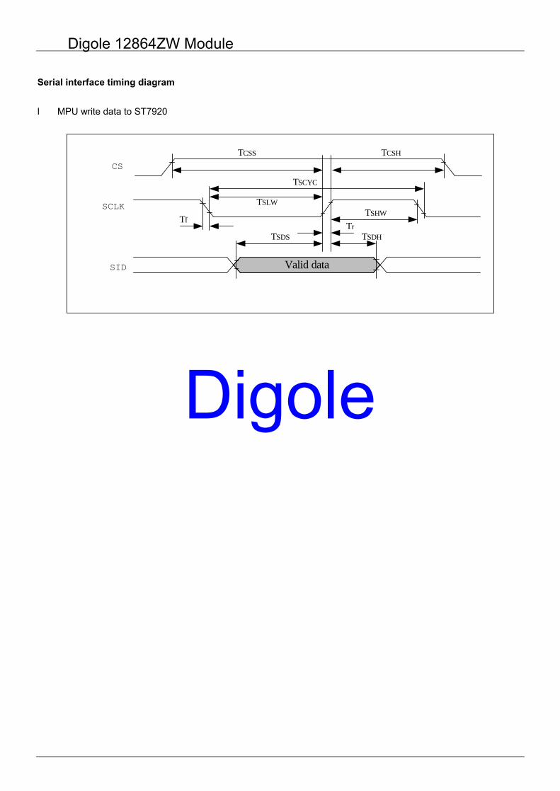
Serial interface timing diagram
l MPU write data to ST7920
Valid data
CS
SID
SCLK
TCSS TCSH
TSCYC
TSLW
TSHW
TSDS
Tr
TSDH
Tf
Digole 12864ZW Module
Digole
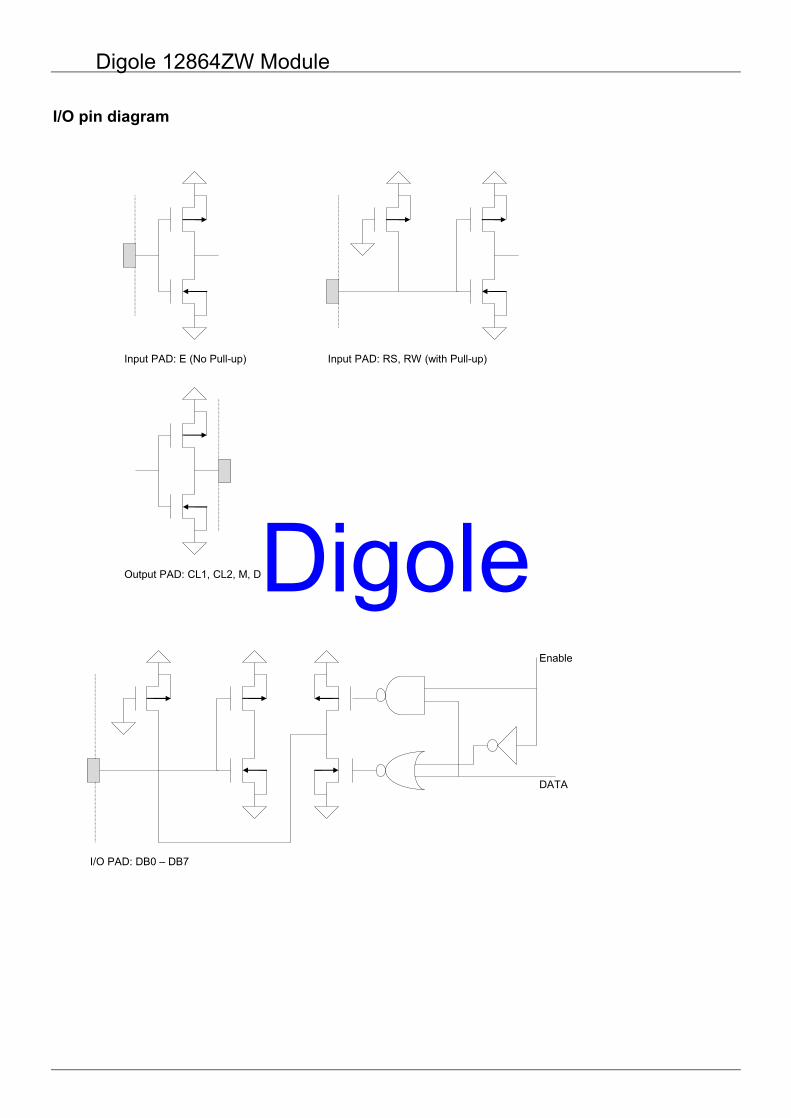
I/O pin diagram
Input PAD: E (No Pull-up) Input PAD: RS, RW (with Pull-up)
Output PAD: CL1, CL2, M, D
I/O PAD: DB0 – DB7
DATA
Enable
Digole 12864ZW Module
Digole
Digole 12864ZW Module