
DIGITAL SIGNAL PROCESSOR ~m~[~i~~mW · DIGITAL SIGNAL PROCESSOR "'~"OMONTo~ c.Le'tar1e (}Jo. \~,z....
20
NEC Microcomputers, Inc. NEC 11- PD7720-- DIGITAL SIGNAL PROCESSOR c.Le'tar1e (}Jo. - • * OESCR I PTION The NEC pPD7720 Signal Processing Interface (SPI) is an advanced-architecture microcomputer optimized for signal processing algorithms. Its speed and flexibility allow the SPI to implement signal processing functions efficiently in a wide range of environments and applications. The N EC SPI is the state of the art in signal processing today, and for the future. APPLICATIONS • Speech Synthesis and AnaJysis PERFORMANCE BENCHMARKS • Digital Filtering • Fast Fourier Transforms (FFT) • Dual-Tone Multi-Frequency (DTMF) Transmitters/Receivers • High Speed Data Modems • Equalizers • Adaptive Control • Sanar/Radar Image Processing • NumericaJ Processing • Second Order Digital Filter (BiQuad) • SINE/COS of Angles • p/A lAW to Linear Conversion • FFT: 32 Point Complex 64 Paint Complex -2.25p.s 5.25p.s 0.50 p.s 0.7 ms 1.6 ms FEATURES • Fast Instruction Execution - 250 ns/8 mHz clock • 16 Bit Data Word • Multi-Operation Instructions for Optimizing Program Execution • large Memory Capacities - Program ROM - Coefficient ROM - Data RAM • Fast (250 ns) 16 x 16 31-Bit Multiplier • Dual Accumulators 512 x 23 Bits 510 x 13 Bits x 16 Bits • Four levei Subroutine Stack for Program Efficiency • Multiple l/O Capabilities - Serial - Parallel - DMA • Compatible with Most Microprocessors, Including: - pPD8080 - pPD8085 - pPD8086 - pPD780 (Z80™*) • Power Supply +5V • NMOS Technology • Package - 28 Pin Dip Rev/l Z80 is a trademark of Zilog Corporation. 173 Woréester StreetIWellesley, Massachusetts 02181 Telephone 617/237-1910 TWX 710·383-1745
Transcript of DIGITAL SIGNAL PROCESSOR ~m~[~i~~mW · DIGITAL SIGNAL PROCESSOR "'~"OMONTo~ c.Le'tar1e (}Jo. \~,z....

NEC Microcomputers, Inc. ~
NEC 11- PD7720--
~m~[~i~~mW
--------~
DIGITAL SIGNAL PROCESSOR "'~"OMONTo~ c.Le'tar1e (}Jo. \~,z. - ~ •
*
OESCR I PTION The NEC pPD7720 Signal Processing Interface (SPI) is an advanced-architecture microcomputer optimized for signal processing algorithms. Its speed and flexibility
allow the SPI to implement signal processing functions efficiently in a wide range of environments and applications.
The N EC SPI is the state of the art in signal processing today, and for the future.
APPLICATIONS • Speech Synthesis and AnaJysis
PERFORMANCE BENCHMARKS
• Digital Filtering • Fast Fourier Transforms (FFT) • Dual-Tone Multi-Frequency (DTMF) Transmitters/Receivers • High Speed Data Modems • Equalizers • Adaptive Control • Sanar/Radar Image Processing • NumericaJ Processing
• Second Order Digital Filter (BiQuad) • SINE/COS of Angles • p/A lAW to Linear Conversion • FFT: 32 Point Complex
64 Paint Complex
-2.25p.s 5.25p.s 0.50 p.s 0.7 ms 1.6 ms
FEATURES • Fast Instruction Execution - 250 ns/8 mHz clock • 16 Bit Data Word • Multi-Operation Instructions for Optimizing Program Execution
• large Memory Capacities - Program ROM - Coefficient ROM - Data RAM
• Fast (250 ns) 16 x 16 31-Bit Multiplier • Dual Accumulators
512 x 23 Bits 510 x 13 Bits 1~8 x 16 Bits
• Four levei Subroutine Stack for Program Efficiency
• Multiple l/O Capabilities - Serial - Parallel - DMA
• Compatible with Most Microprocessors, Including: - pPD8080 - pPD8085 - pPD8086 - pPD780 (Z80™*)
• Power Supply +5V • NMOS Technology • Package - 28 Pin Dip
Rev/l
Z80 is a trademark of Zilog Corporation.
173 Woréester StreetIWellesley, Massachusetts 02181 Telephone 617/237-1910 TWX 710·383-1745

Jl-PD7720 NC VCC PIN CONFIGURATION
~ AO ORO ~
PO 1m" P1 5 WR"
DO 6 SORO
01 7 pPD7720D 50
02 8 SI
03 ~
04 "SJ'E'N" 05 SCK
06 INT
07 RST
GNO CLK
Fabricated in high-speed NMOS, the IlPD7720 SPI is a complete 16-bit microcomputer FUNCTIONAL DESCRIPTION on a single chip. ROM space is provided for program and coefficient storage, while the on-chip RAM may be used for temporary data, coefficients and results. Computa-tional power is provided by a 16-bit Arithmetic/Logic Unit (ALU) and a separate 16 x ·16 bit fully parallel multiplier. This combination allows the implementation of a "sum of products" operation in a single 250 nsec instruction cycle. In addition, each arithmetic instruction provides for a number of data movement operations to further
. increase throughput. Two serial I/O ports are provided for interfacing to codecs and other serially-oriented devices while a parallel port provides both data and status information to conventionalllP for more sophisticated applications. Handshaking signals, including DMA controls, allow the' SPI to act as a sophisticated programmable
~ ,-
peripheral as well as a stand alone microcomputer. ~
Memory is divided into three types: Program ROM, Data ROM, and Data RAM. MEMORY ', ___ /L
The 512 x 23 bit words of Program ROM are addressed by a 9-bit Program Counter which can be modified by an externai reset, interrupt, call, jump, or return instruction.
The Data ROM is organized in 512 x 13 bit words and is also addressed through a 9-bit ROM pointer (RP Reg.) which may be modified as part of an arithmetic instruction
50 that the next value is available for the next instruction. The Data ROM is ideal for storing the necessary coefficients, conversion tables and other constants for ali your processing needs.
The Data RAM is 128 x 16 bit words and is addressed through a 7-bit Data Pointer (DP Reg.). The DP has extensive addressing features that operate simultaneously with arithmetic instructions 50 that no added time is taken for addressing or address modification. . ~i<', l5XfR
ORQ
STACK
S
FLAGA ~
FLAGB
CLK_~ RST_
INT VCC_
o ;'No- INTERRUPT
INSTRUCTION ROM
512x 23
s c z o o A A A V V
RAio! 128.16
o A A 14+--...........
o o v V B o
MULTIPLIER
BLOCK DIAGRAM
~--

11- PD7720
PIN IDENTIFICATION PIN NAME 1/0 FUNCTION
1 NC I No Connection.
2 õACi< I DMA Request Acknowledge. Indicates to the ",PD7720 that the Data Bus is ready for a DMA transfer. (DACK ; CS o AO; O;
3 ORO O DMA Request signals that the ",PD7720 is requesti ng a data transfer on the Data Bus.
4.5 PO. P1 O PO. P1 are general purpose output control tines.
6-13 00-0 7 1/0 Tristate Port for data transfer between the Data Register or Status Register and Data Bus.
14 GND
15 CLK I Single phase Master Clock input.
16 RST I Reset initializes the ",PD7720 internai logic and sets the PC to O.
17 INT I Interrupt. A low to high transition on this pin will (lf interrupts are enabled by the program) execute a call instruction to location 100H.
18 SCK I Serial Data Input/Output Clock.
19 SIEN I Serial Input Enable. This tine enables the shift
. clock to the Serial Input Register .
--20 SOEN I Serial Output Enable. This pin enables the shift clock to the Serial Output Register.
21 SI I Serial Data Input. This pin inputs 8 or 16 bit serial data words from an externai device such as an A/D ,converter.
22 SO O Serial Data Qutput. This pin outputs 8 or 16 bit data words to an externai device such as an D/A converter.
23 SORO O Serial Data Output Request. Specifies to an externai device that the Serial Data Register has been loaded and is ready for output. SORO is reset when the entire 8 or 16 bit word has been transferred.
-24 WR I Write Control Signal writes the contents of data bus into the Data Register.
25 Rõ I Read Control Signal. Enables an output to the Data Port from the Data or Status Register.
26 CS I Chip Select. Enables data transfer with Data or Status Port with RD or WR.
27 AO I Selects Data Register for Read/Write (Jow) or Status Register for read (high).
28 VCC +5V Power
3

p.PD7720
General
One of the unique features of the SPI's architecture is its arithmetic facilities. With a separate multipler, ALU, and multiple internai data paths, the SPI is capable of carrying out a multiply, an add, or other arithmetic operation, and moving data between internai registers in a single instruction cycle.
ALU
The ALU is a 16-bit 2's complement unit capable of executing 16 distinctoperations on virtually any of the SPI's internai registers, thus giving the SPI both speed and versatility for efficient data management.
Accumulators (ACCA/ACCB)
Associated with the ALU are a pair of 16-bit accumulators, each with its own set of flags, which are updated at the end of each arithmetic instruction (except NOP). In addition to Zero Result, Sign Carry, and Overflow Flags, the SPI incorporate5 auxilliary Overflow and Sign Flags (SAl, SB1, OVAl, OVal). These flag5 enable the detection of an overflow condition and maintain the correct sign up to as many as 3 successive additions or subtractions.
FLAGA
FLAG a
SAl
SBl
SAO
SBO
CA ZA OVAl
CB ZB OVBl
ACC A/B FLAG REGISTERS
Sign Register (SGN)
OVAO
OVBO
When OVA 1 (or OVB 1) is set, the SA 1 (or S8 1) bit will hold the corrected sign of the overflow. The SGN Register will use SA 1 (SB 1) to automatically generate saturation constants 7FFFH(+) or 8000H(-) to permit efficient limiting of a calculated value.
Multiplier
Thirty-one bit results are developed bya 16 x 16-bit 2's complement multiplier in 250 ns. The result is automatically latched in 2 16-bit registers M&N (LSB in N is zero) at the end of each instruction cycle. The ability to have a new product available, and to be able to use it in each instruction cycle, provides significant advantages in maximizing processing speed for real time signal processing.
Stack
The SPI contains a 4-level program stack for efficient program usage and interrupt handling.
Interrupt
A single levei interrupt is supported by the SPI. Upon sensing a high levei on the INT terminal, a subroutine call to location 100H is executed. The EI bit of the status register is automatically reset to O thus disabling the interrupt facilities until reenabled under program control.
4
ARITHMETIC CAPABILITIES

_1""\
------ ------I'PD7720
INPUT/OUTPUT General
The NEC SPI has 3 communication ports: 2 serial and one 8-bit parallel, each with their own controllines for interface handshaking. The pa~allel port also includes DMA controllines (ORO and DACK) for high speed data transfer and reduced processor
overhead. A general purpose 2 bit output (see Figure 1) port rounds out a'full com plement of interface capability .
SUS
INTERFACE (SUS)
..
~MA { INTERFACE
INTERRUPT
RESET CLOCK
Serial 1/0
.Ao
." .;> ~
-
00-07
Rõ WA cs Ao
-OACK
ORQ
INT
RST CLK
SO' SORQ SOEN
SCK "P07720
SI'
SIEN
Po
P1
~
-~
SERIAL 1/0 INTERFACE
} OUTPUT PORT
Two shift registers (SI, SO) that are software-configurable to 8 or 16 bits and are
externally clocked (SCK) provide simple interface between the SPI and serial peripherals such as AIO and DIA converters, codecs, or other SPls.
SERIAL 1/0 TIMING
SCK
SOA0
SõêN
R ___ ..... 1 ,--------------\~--------~R------------JL------------
OUTPUT DATA
SOACK -l
HIGHZ <D o .----HIGH Z 160A _,'-______ _
SOLOAD~~ _________________________ .r_-_-_-_--~; _______ ___
\~------___________________________ _JI
SIAEG ---------__________________________________ ~r1~ ______ ___
LOAD PULSE ,..-----, SIACK ---------------------------------------~I L---
<D Data clocked OUl on faUing c:dgo of SCK. and valid on rísíng of SCK.
@ Data clocked In on rlslng edge of SCK. @ Broken Une denotes consecutlve S8nding Df next date.
PARALLEL I/O The 8-bit parallel I/O port may be used for transferring data or reading the SPI's status. Data transfer is handled through a 16-bit Data Register (DR) that is softwareconfigurable for double or single byte data transfers. The port is ideally suited for operating with 8080, 8085 and 8086 processo r buses and may be used with other processors and computer systems.
5

Jl-PD7720
PARALLEL RJW OPERATION
CS AO WR RD OPERATION
1 X X ~} { No effect on internai operation. 00-07 are at X X 1 high impedance leveis.
O O O 1 Data from 00-07 is latched to OR CD O O 1 O Contents of O R are output to 00-0 7 <D O 1 O 1 lIIegal
O 1 1 O Eight MSBs of SR are output to 00-07
O X O O lIIegal
<D Eight MSBs or 8 LSBs of data register (OR) are used depending on OR status bit (ORS). The condition of OACK = O is equivalent to AO = CS = O.
Status Register (SR)
MSB LSB
The status register. is a 16-bit register in which the 8 most significant bits may be read by the system's MPU for the latest 1/0 and processing status.
ROM - (Request for Master): A read or write from OR to 10B sets ROM = 1. An Ext read (write) resets ROM = O.
USFl - (User Flag 1):} USFO - (User Flag O):
ORS - (OR Status):
OMA- (OMA Enable):
ORC - (OR Contrai):
soe - (SO Control):
SIC - (SI Control):
EI - (Enable Interrupt):
PO/Pl (Ports O and 1):
6
General purpose flags which may be read by an externai processo r for user defined signalling
For 16 bit OR transfers (ORC = O) ORS = 1 after first 8 bits have been transferred, ORS = O after ali 16 bits
OMA = O (Non OMA transfer mode) OMA = 1 (OMA transfer mode)
ORC = O (16 bit mode), ORC = 1 (8 bit mode)
SOC = O (16 bit mode), SOC = 1 (8 bit mode)
'SIC = O (16 bit mode), SIC = 1 (8 bit mode)
EI = O (interrupts disabled), EI = 1 (interrupts enabled)
PO and Pl directly contrai the state of output pins PO and Pl

p.PD7720
INSTRUCTIONS The SPI has 3 types of instructions ali of which are one word, 23 bits long and execute in 250 ns.
A) Arithmetic/Move-Return (OP = OO/RT = 01)
22 21 20 19 18 17 16 15 14 13 12 11 10 9 8 7 6 5 4 3 2 1 O
OP O O P- ·1
li ~ ALU 5 OPL OPH·M D SRC OST
SELECT L c R
RT O 1 Same as OP instruction
There are two instructions of this type, both of which are capable of executing ali ALU functions listed in Table 2 on the value specified by the.ALU input, i.e., P Select Field (see Table 1).
Table 1. OP, RT
P Select Field
Mnemonic 020 019 ALU Input
RAM O O RAM
10B O 1 *Internal Data Bus
M 1 O M Register
N 1 1 N Register
* Any value on the on-chip data bus. Value may be selected from any of registers listed In Table 7 source reglster selectlons.
7

p.PD7720
ALU Field
Mnemonic 018 017 016 015
NOP O O O O OR O O O 1 ANO O O 1 O
XOR O O 1 1 SUB O 1 O O
AOO O 1 O 1
SBB O 1 1 O
ADC O 1 1 1
DEC 1 O O O INC 1 O O 1 CMP 1 O 1 O
SHRl 1 O 1 1
SHLl 1 1 O O SHL2 1 1 O 1
SHL4 1 1 1 O XCHG 1 1 1 1
* May bo affec:ted. dcpondlng on dto mults - Previoul I1IttUI can bo hold Cf Ruot X Indeflnlto
Table 2. OP, RT Flags Affectad
FisgA SA1 SAO CA ZA OVA1 OVAO
ALU Function FlagB SB1 SBO CB ZB OVB1 OVBO
No Operation - - - - - -OR X * " * d d
ANO X * d * d d
ExclusiveOR X * " * " d
Subtract * * * * * * AOO * * * * * * Subtract with * * * * * * Borrow
Add with Carry * * * * * * Decrement ACC * * * * * * Increment Acc * * * * * * Complement ACC X * " * 0 0 (1'$ Complement)
l-bit R·Shift X * * * d 0 1-bit L·Shift X * * * d 0 2-bit L·Shift X * (I * d 0 4-bit L·Shift X * " * 0 0 8-bit Exchange X * d * 0 0
Table 3. OP, RT
ASL Field
Mnemonic 014 Aee Selection
ACCA O ACCA ACCB 1 ACCB
Table 4. OP, RT
OPL Field
Mnemonic 013 012 OP3-0PO
OPNOP O O No Operation
OPINC O 1 Increment OPL opoec 1 O Oecrement OPL OPCLR 1 1 Clear OPL
Table S. OP, RT
OPH-M Field
Mnemonic 011 010 09 Exclusive OR
MO O O O (OP6 OPS OP4)),J. (O O O)
M1 O O 1 OP6 OPS OP4 ),J. (O O 1)
M2 O 1 O OP6 OPS ,OP4 ),J. (O 1 O)
M3 O 1 1 OP6 OPS OP4 ),J. (O 1 1)
M4 1 O O OP6 OPS OP4 ),J. (1 O O)
MS 1 O 1 OP6 OPS OP4 ),J. (1 O 1).
M6 1 1 O OP6 OPS OP4 ),J. (1 1 O)
M7 1 1 1 OPa OPs OP4 ),J. (1 1 1)
8

-~
",PD7720
Table 6. OP,RT
RPOCR
Mnemonic Os Operation
RPNOP O No Operation
RPDEC 1 Decrement RP
Besides the arithmetic functions these instructions can also modify (1) the RAM Data Pointer DP, (2) the Data ROM Pointer RP, and (3) move data along the on-chip data bus from a source register to a destination register (the possible source and destination registers are listed in Tables 7 and 8 respectively). The difference in the two ii1Structions of this type is that one executes a subroutine or interrupt return at the end of the instruction cycle while the other does noto
Table 7. OP, RT
SRC Field
Mnemonic 07 06 05 04 Specified Register
NON O O O O NO Register
A O O O 1 ACC A (Accumulator A)
B O O 1 O ACC B (Accumulator B)
TR O O 1 1 TR Temporary Register
DP O 1 O O DP Data Pointer
RP O 1 O 1 RP ROM Pointer
RO O 1 1 O RO ROM Output Data
SGN O 1 1 1 SGN Sign Register
DR 1 O O O O R Data Register
DRNF 1 O O 1 DR Data No Flag <D SR 1 O 1 O SR Status
SIM 1 O 1 1 SI Serial in MSB ® SIL 1 1 O O SI Serial in LSB @
K 1 1 O 1 K Register
L 1 1 1 O L Register
MEM 1 . 1 1 1 RAM
<D DR to IDB ROM not set. IN DMA ORO not set. ~ First bit in goes to MSB, last bit to LSB. @ First bit in goes to LSB, last bit to MSB (bit reversed).
Table 7 - List of Registers Specified by the Source Field (SRC)
9

;.
-
jl.PD7720 Table 8. OP, RT, LO
OST Field
Mnemonic 03 02 01 DO Specified Register
@NON O O O O NO Register
@A O O O 1 ACC A (Accumulator A)
@B O O 1 O ACC B (Accumulator B)
@TR O O 1 1 TR Temporary Register
@DP O 1
@RP O 1
@OR O 1
@SR O 1
@SOL 1 O
@SOM 1 O
@K 1 O
@KLR 1 O
@KLM 1 1
@L 1 1
@NON 1 1
@MEM 1 1
<D LSB is first bit out. ~ MSB is first bit out.
·0
O
1
1
O
O
1
1
O
O
1
1
O OP Data Pointer
1 RP ROM Pointer
O DR Data Register
1 SR Status Register
O 50 Serial Out LSB <D 1 50 Serial Out MSB ~ O K (Mult)
1 10 B -+ K ROM -+ L @
O Hi RAM -+ K IDB -+ L
1 L (Mult)
O NO Register
1 RAM
@ Internai data bus to K and ROM to L register.
@
® Contents of RAM address specified by OP6 = 1 (Le., 1, OPS, OP4,-OPO) is placed in K register. IOB is placed in L.
- Table 8 - List of Registers Specified by the Oestination Field (OST)
B) Jump/Call/Branch
22 21 20 19 18 17 16 15 14 13 12 11 10 9 8 7 6 5 4 3 2 1 O
10 BRCH CND NA
JP Instruction Field Specifications
Three types of execution address modification instructions are accommodated by the processor and are listed in Table 9. Ali of the instructions, if unconditional or the specified condition is true, take their next program execution address from the Next Address field (NA), otherwise PC = PC + 1.
Table 9. Branch Field Selections (BRCH)
20 19 18 I nstruction
1 O O Unconditional jump
1 O 1 Subroutine call
O 1 .0 Conditional jump
For the conditional jump instruction, the condition field specifies the jump condition. Table 10 lists ali the instruction mnemonics of the J/C/B OP codes.
The SPI offers ali the execution modification instructions necessary for efficient data, 1/0 and arithmetic control.
10
~\

p.PD7720
Table 10. Condition Field Specifications
BRCH/CNO Fields
Mnemonic °20 °19 018 ·°17 °16 015 °14 °13 Conditions
JMP 1 O· O O O O O O Unconditional
CALL 1 O 1 O O O O O Unconditional
JNCA O 1 O O O O O O CA=O
JCA O 1 O O O O O 1 CA= 1
JNCB O 1 O O O O 1 O CB=O
JCB O 1 O O O O 1 1 CB = 1
JNZA O 1 O o" O 1 O O ZA=O
JZA O 1 O O O 1 O 1 ZA= 1
JNZB O 1 O O O 1 1 O ZB=O
JZB O 1 O O O 1 1 1 ZB = 1
JNOVAO O 1 O O 1 O O O OVAO=,O
JOVAO O 1 O O 1 O O 1 OVAO= 1
JNOVBO O 1 O O 1 O 1 O OVBO= O
JOVBO O 1 O O 1 O 1 1 OVBO= 1
JNOVA1 O 1 O O 1 1 O O OVA1 =·0 .~, JOVA1 O 1 O O 1 1 O 1 OVA1=1
JNOVB1 O 1 O O 1 1 1 O OVB1=0
JOVB1 O 1 O O 1 1 1 1 OVB1 = 1
JNSAO O 1 O 1 O O O O SAO=O
JSAO O 1 O 1 O O O 1 SAO= 1
JNSBO O 1 O 1 O O 1 O SBO= O
JSBO O 1 O 1 O O 1 1 SBO= 1
JNSA1 O 1 O 1 O 1 O O SA1 = O
JSA1 O 1 O 1 O 1 O 1 SA1 = 1
JNSB1 O 1 O 1 O 1 1 O SB1 = O
JSB1 O 1 O 1 O 1 1 1 SB1 = 1
JOPLO O 1 O 1 1 O O O OPL =0
JOPLF O 1 O 1 1 O O 1 OPL = F (HEX)
JNSIAK O 1 O 1 1 O 1 O SI ACK= O
JSIAK O 1 O 1 1 O 1 1 SI ACK= 1
JNSOAK O 1 O 1 1 1 O O SO ACK = O
JSOAK O 1 O 1 1 1 O 1 SO ACK= l
JNROM O 1 O 1 1 1 1 O ROM=O
JROM O 1 O 1 1 1 1 1 ROM= 1
*BRCH or CNO values not in this table are prohibited.
11

~PD7720
C) Load Data (LO)
22 21 20 19 18 17 16 15 14 13 12 11 10 9 8 7 6 5 4 3 2 1 O
10
The Load Data instruction will take the 16-bit value containedin the Immediate Data field (I D) and place it in the location specified by the Destination field (DST) (see Table 8),
Load Data Field Specifications
INT'L CLK I tP2 I tP3 I tP4 I tP1 I tP2 I tP3 I t/>4 I tP1 I tP2 I ROM AOORESS '---I '---I INST LATCH
REGISTER AOORESS
RAM AOORESS
INTERNAL BUS
____ -=>-c: ______________ ~ ____________ _'=>
I ,~ ____ -'I ,----REG ISTER 8 RAM WRITE ALU INPUT ---___ _'r-\~ _______ .Jr__\ ___ _
ALU OUTPUT
ACC LATCH
MULTIPLlER SET
12
========~><~======~~----________ J~~ _____________ _
INSTRUCTION EXECUTION TIMING

p.PD7720
ABSOLUTE MAXIMUM Voltage (VCC Pin) .............•................ -0.5 to +7.0 Volts <D RATINGS* Voltage, Any Input ................•..•.......... -0.5 to +7.0 Volts <t
DC CHARACTERISTICS
CAPACITANCE
Voltage, Any Output ............................. -0.5 to +7.0 Volts <D Operating Temperature ......•....................... -10°C to +70oC Storage Temperature .......................•....... -65°C to +150°C
Note: <D With respect to GND.
COMMENT: Exposing the device to stresses above those Iisted in Absolute Maximum Ratinos could cause permanent damage. The deviee is not meant to be operated under conditions outside the fimits deseribed in the operational sections of this speeification. Exposure to absolute maximum rating eonditions for extended periods mav affeet device reliabilitv.
Ta c-lO - +70°C, VCC = +5V ± 5%
PARAMETER SVMBOL MIN TVP MAX UNIT CONDITION
Input Low Voltage VIL -0.5 0.8 V
Input High Voltage VIH 2.0 VCC+O·5 V
CLK Low Voltage Vt/>L -0.5 0.45 V
CLK High Voltage Vt/>H 3.5 VCC+O·6 V
Output Low Voltage VOL 0.46 V IOL; 2.0 mA
Output High Voltage VOH 2.4 V IOH =-400pA
Input Load Current ILIL -10 JJA VIN"'OV
Input Load Current ILIH 10 p.A VIN=VCC
Output Float Leakage ILOL -10 JJA VOUT"'O.47V
Output Float Leakage ILOH 10 p.A VOUT"'VCC
Power SupplV Current ICC 180 280 mA
PARAMETER SVMBOL MIN TVP MAX UNIT CONDITION
CLK, SCK Input Ct/J 20 pF Capaeltance
Input Pin Capaeitanee CIN 10 pF fe:: 1 MHz
Output Pin Cap~eitance COUT 20 pF
13

,uPD7720
PARAMETER SVMBOL MIN TVP
CLK Cycle Time rpCY 123
CLK Pulse Width rpD 60
CLK Rise Time rpR
CLK Fali Time rpF
Address Setup Time for RD tAR O
Address Hold Time for Ao tRA O
RD Pulse Width tRR 250
Data Delay from Ao tRD
Read to Data Floatlng tDF 10
Address Setup Time for WR tAW O
Address Hold Time for WR tWA O
WR Pulse Wldth tww 250
Data Setup Time for WR tDW 150
Data Hold Time for WR tWD O
ORO Delay tAM
SCK Cycle Time tSCY 480
SCK Pulse Width tSCK 230
SCK Rise/Fall Time tRSC
SORO Delay tORa 30
SOEN Setup Time tsoc 50
SOEN Hold Time tcso 30
SO Delay tDCK
SO Delay from SORO tDZRO *
SO Delay from SCK tDZSC *
SO Delay from SOEN tOZE *
SOEN to SO Floating tHZE *
SCK to SO Floatlng tHZSC *
SORO to SO Floating tHZRO 70
SIEN, SI Setup Time tDC 50
SIEN, SI Hold Time tCD 30
PO, P1 Delay top
RST Pulse Width tRST 4
INT Pulse Width tlNT 8
*To be specified
G) Voltage at measuring point of timing 1.0V and 3.0V
14
MAX
2000
10
10
150
100
150
DC
20
150
150
300
300
180
300
200
300
IPCY + 150
UNIT
ns
ns
ns
ns
ns
ns
ns
ns
ns
ns
ns
ns
ns
ns
ns
ns
ns
ns
ns
ns
ns
ns
ns
ns
ns
ns
ns
ns
ns
ns
ns
rpCY
rpCY
CONDITION
<D <D
CL::: 100 pF
CL:::100pF
CL::: 100 pF
CL"'100pF
AC CHARACTERISTICS
(
-.

---------
JI. PD7720
TIMING WAVEFORMS
CLOCK
CLK ___ JI
CPf
READ OPERATION
~---tRR----.. -I1 tRAt----RO-----
DBO_7------------:~1:---tDF f------
15 .

P.PD7720
WRITE OPERATION
AO, CS, õACK )(
---~tAW ... '24----
WR----~ ~ )~ I;
OI ~ ~
~~----------------)
TIMING WAVEFORMS (CONT.)
--~: 080-7 ---------------
tOw-..... ~'~.I-~Dl ___ _
DMA OPERATION
OACK /
ORO /
. 16
~ '" .. '
-...
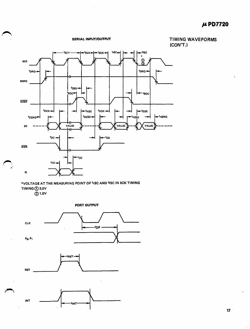
SERIAL INPUT/OUTPUT
SCK
SORQ ----11-1
!so
tOZR
tsoc
r tOZE
tHZ;~ =-r-tHZRQ
,.,.PD7720
TIMING WAVEFORMS (CON'T.)
SO -{X3------
SI
*VOLTAGE AT THE MEASURING POINT OF trsc ANO tfSC IN SCK TIMING
TIMING <D 3.0V
@1.0V
PORTOUTPUT
CLK
___ I
RST
INT
17

JI. PD7720
18
SENSOR
MICROPHONE THERMAL PRESSURE LlGHT
BANDLIMITING FILTER
ANANALOGTO ANALOG DIGITAL PROCESSING SYSTEM USING A SINGLE SPI
ANALOG IN AIO
SPI (FFT)
PRODUCT EXAMPLE P • USING THE "PD7720 .. . ..
DATA & DISPLAY I---~
CONTROl
. . : . ...• ,: ... . ........ : ...
FREQ~
SPECTRUM ANAL YSIS SYSTEM
SCK
SI SO "PD7720 DIA R.F.
ANALOG
mm mEN OUT
TXRQ
REC'ONSTRUCTION FILTER
1/0 CONTROL
r\ .' -

SCK SCK
1---"" SI SOI---........ SPI SPI
..... -.,.....~m-EIif 501----..... SI SORO 1-------...
A SIGNAL PROCESSING SVSTEM USING SPl(s) AS A COMPLEX COMPUTE R PERIPHERAL
"SO"EN' ãõEN
• • •
A SIGNAL PROCESSING SVSTEM USING CASCAOEO SPls & SERIAL COMMUNICATION.
HOST MEMORV CPU
B
OR01
õAcKl OMA
CONTROLLER
• • • • • • OROen) SI
SPI õACi«n)
SO
JI. PD7720
ANALOG OUT
19

, i ..
...
'" PD7720
. '
• The information presented in this docu'ment is believed to be accurate and reliable. It is s.ubject to change without notice .
. @1981 NEC Microcomputers, rnc. Printed in U.S.A. 77200S·ÃEV1·1-8108K
20
,i~ .
i~ .... ___ .i'
fmontoro
Texto digitado
fmontoro
Texto digitado
Fabio Montoro


