DSP56156 16-Bit Digital Signal Processor
76
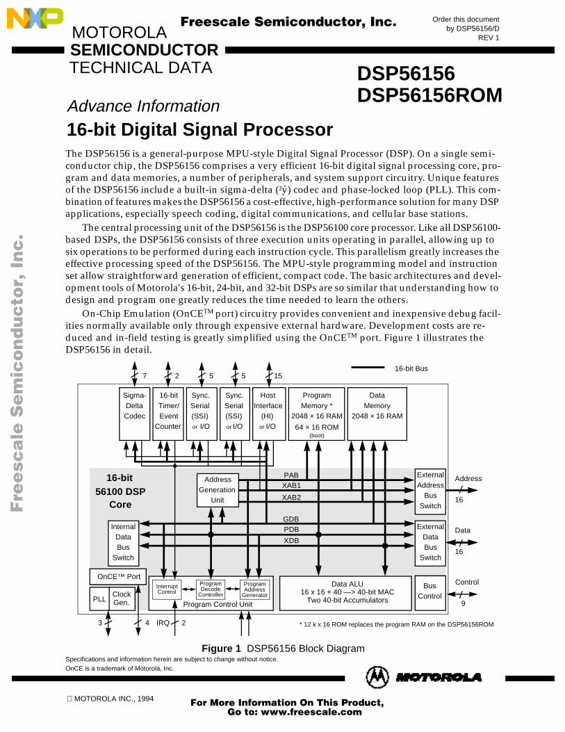
MOTOROLA INC., 1994 MOTOROLA TECHNICAL DATA SEMICONDUCTOR The DSP56156 is a general-purpose MPU-style Digital Signal Processor (DSP). On a single semi- conductor chip, the DSP56156 comprises a very efficient 16-bit digital signal processing core, pro- gram and data memories, a number of peripherals, and system support circuitry. Unique features of the DSP56156 include a built-in sigma-delta (²ý) codec and phase-locked loop (PLL). This com- bination of features makes the DSP56156 a cost-effective, high-performance solution for many DSP applications, especially speech coding, digital communications, and cellular base stations. The central processing unit of the DSP56156 is the DSP56100 core processor. Like all DSP56100- based DSPs, the DSP56156 consists of three execution units operating in parallel, allowing up to six operations to be performed during each instruction cycle. This parallelism greatly increases the effective processing speed of the DSP56156. The MPU-style programming model and instruction set allow straightforward generation of efficient, compact code. The basic architectures and devel- opment tools of Motorola's 16-bit, 24-bit, and 32-bit DSPs are so similar that understanding how to design and program one greatly reduces the time needed to learn the others. On-Chip Emulation (OnCE TM port) circuitry provides convenient and inexpensive debug facil- ities normally available only through expensive external hardware. Development costs are re- duced and in-field testing is greatly simplified using the OnCE TM port. Figure 1 illustrates the DSP56156 in detail. Figure 1 DSP56156 Block Diagram Specifications and information herein are subject to change without notice. OnCE is a trademark of Motorola, Inc. Data 16 Control 9 Address 16 Data ALU 16 x 16 + 40 —> 40-bit MAC Two 40-bit Accumulators PLL Clock Gen. GDB PDB XDB Internal Data Bus Switch External Data Bus Switch Bus Control PAB XAB1 XAB2 Address Generation Unit External Address Bus Switch IRQ 2 16-bit Bus 16-bit 56100 DSP Core Program Address Generator Program Decode Controller Interrupt Control Program Control Unit Sigma- Delta Codec 4 3 OnCE™ Port 16-bit Timer/ Event Counter Sync. Serial (SSI) or I/O Host Interface (HI) or I/O 5 15 2 (boot) Sync. Serial (SSI) or I/O 5 7 Data Memory 2048 × 16 RAM Program Memory * 2048 × 16 RAM 64 × 16 ROM * 12 k x 16 ROM replaces the program RAM on the DSP56156ROM Advance Information 16-bit Digital Signal Processor DSP56156 Order this document by DSP56156/D REV 1 DSP56156ROM Freescale Semiconductor, I Freescale Semiconductor, Inc. For More Information On This Product, Go to: www.freescale.com nc...
Transcript of DSP56156 16-Bit Digital Signal Processor
MOTOROLA INC., 1994
MOTOROLA
TECHNICAL DATASEMICONDUCTOR
The DSP56156 is a general-purpose MPU-style Digital Signal Processor (DSP). On a single semi-conductor chip, the DSP56156 comprises a very efficient 16-bit digital signal processing core, pro-gram and data memories, a number of peripherals, and system support circuitry. Unique features of the DSP56156 include a built-in sigma-delta (²ý) codec and phase-locked loop (PLL). This com-bination of features makes the DSP56156 a cost-effective, high-performance solution for many DSP applications, especially speech coding, digital communications, and cellular base stations.
The central processing unit of the DSP56156 is the DSP56100 core processor. Like all DSP56100-based DSPs, the DSP56156 consists of three execution units operating in parallel, allowing up to six operations to be performed during each instruction cycle. This parallelism greatly increases the effective processing speed of the DSP56156. The MPU-style programming model and instruction set allow straightforward generation of efficient, compact code. The basic architectures and devel-opment tools of Motorola's 16-bit, 24-bit, and 32-bit DSPs are so similar that understanding how to design and program one greatly reduces the time needed to learn the others.
On-Chip Emulation (OnCETM port) circuitry provides convenient and inexpensive debug facil-ities normally available only through expensive external hardware. Development costs are re-duced and in-field testing is greatly simplified using the OnCETM port. Figure 1 illustrates the DSP56156 in detail.
Figure 1 DSP56156 Block DiagramSpecifications and information herein are subject to change without notice.OnCE is a trademark of Motorola, Inc.
Data
16
Control
9
Address
16
Data ALU16 x 16 + 40 —> 40-bit MAC
Two 40-bit AccumulatorsPLLClockGen.
GDBPDB
XDB
InternalDataBus
Switch
ExternalDataBus
Switch
BusControl
PABXAB1
XAB2
AddressGeneration
Unit
ExternalAddress
BusSwitch
IRQ 2
16-bit Bus
16-bit56100 DSP
Core
ProgramAddress
Generator
ProgramDecode
Controller
InterruptControl
Program Control Unit
Sigma- Delta Codec
43
OnCE™ Port
16-bit Timer/Event
Counter
Sync.Serial (SSI) or I/O
Host Interface
(HI) or I/O
5 15 2
(boot)
Sync.Serial (SSI) or I/O
5 7
DataMemory
2048 × 16 RAM
ProgramMemory *
2048 × 16 RAM
64 × 16 ROM
* 12 k x 16 ROM replaces the program RAM on the DSP56156ROM
Advance Information16-bit Digital Signal Processor
DSP56156
Order this documentby DSP56156/D
REV 1
DSP56156ROM
Fre
esc
ale
Se
mic
on
du
cto
r, I
Freescale Semiconductor, Inc.
For More Information On This Product, Go to: www.freescale.com
nc
...

2 DSP56156 Data Sheet MOTOROLA
Introduction
DSP56156 Features
Digital Signal Processing Core• Efficient, object code compatible, 16-bit 56100-Family DSP engine
— Up to 30 Million Instructions Per Second (MIPS) – 33 ns instruction cycle at 60 MHz— Up to 180 Million Operations Per Second (MOPS) at 60 MHz— Highly parallel instruction set with unique DSP addressing modes— Two 40-bit accumulators including extension byte— Parallel 16 × 16-bit multiply-accumulate in 1 instruction cycle (2 clock cycles)— Double precision 32 × 32-bit multiply with 72-bit result in 6 instruction cycles— Least Mean Square (LMS) adaptive loop filter in 2 instructions— 40-bit Addition/Subtraction in 1 instruction cycle— Fractional and integer arithmetic with support for multiprecision arithmetic — Hardware support for block-floating point FFT— Hardware-nested DO loops including infinite loops— Zero-overhead fast interrupts (2 instruction cycles)— Three 16-bit internal data buses and three 16-bit internal address buses for
maximum information transfer on-chip
Memory• On-chip Harvard architecture permitting simultaneous accesses to program
and memories
• 2048 × 16-bit on-chip program RAM and 64 × 16-bit bootstrap ROM(or 12 k × 16-bit on-chip program ROM on the DSP56156ROM)
• 2048 × 16-bit on-chip data RAM
• External memory expansion with 16-bit address and data buses
• Bootstrap loading from external data bus, Host Interface, or Synchronous Serial Interface
Peripheral and Support Circuits• Byte-wide Host Interface (HI) with Direct Memory Access support
• Two Synchronous Serial Interfaces (SSI) to communicate with codecs and synchronous serial devices
— Built in µ-law and A-law compression/expansion— Up to 32 software-selectable time slots in network mode
• 16-bit Timer/Event Counter also generates and measures digital waveforms
• On-chip sigma-delta voice band Codec:
— Sampling clock rates between 100 kHz and 3 MHz— Four software-programmable decimation/interpolation ratios— Internal voltage reference ( 2/5 of positive power supply)— No external components required
DSP56156 Features
Fre
esc
ale
Se
mic
on
du
cto
r, I
Freescale Semiconductor, Inc.
For More Information On This Product, Go to: www.freescale.com
nc
...

MOTOROLA DSP56156 Data Sheet 3
Introduction
• On-chip peripheral registers memory mapped in data memory space
• Double buffered peripherals
• Up to 27 general purpose I/O pins
• Two external interrupt request pins
• On-Chip Emulation (OnCE™) port for unobtrusive, processor speed-independent debugging
• Software-programmable, Phase-Locked Loop-based (PLL) frequency synthesizer for the core clock
Miscellaneous Features• Power-saving Wait and Stop modes
• Fully static, HCMOS design for operating frequencies from 40 or 60 MHz down to DC
• 112-pin Ceramic Quad Flat Pack (CQFP) surface-mount package; 20 × 20 × 3 mm
• 112-pin Plastic Thin Quad Flat Pack (TQFP) surface-mount package; 20 × 20 × 1.5 mm
• 5 V power supply
Product DocumentationThis data sheet plus the two manuals listed in Table 1 are required for a complete DSP56156 description and are necessary to properly design with the part. Documentation is available from a local Motorola distributor, a semiconductor sales office, or through a Motorola Litera-ture Distribution Center.
Table 1 DSP56156 Documentation
Topic Description Order Number
DSP56100 Family Manual Detailed description of the 56000-family architecture and the 16-bit core processor and instruction set
DSP56100FAMUM/AD
DSP56156 User’s Manual Detailed description of memory, peripherals, and interfaces
DSP56156UM/AD
DSP56156 Data Sheet Pin and package descriptions, and electrical and timing specifications
DSP56156/D
DSP56156 FeaturesDocumentation
Fre
esc
ale
Se
mic
on
du
cto
r, I
Freescale Semiconductor, Inc.
For More Information On This Product, Go to: www.freescale.com
nc
...

4 DSP56156 Data Sheet MOTOROLA
Introduction
Related DocumentationTable 2 lists additional documentation relevant to the DSP56156.
Data Sheet ContentsThis data sheet contains:
• signal definitions and pin locations• electrical specifications and timings• package descriptions• design considerations• ordering information
Table 2 Related Motorola Documentation
Topic Description Order Number
DSP Family Brochure Overview of all DSP product families BR1105/D
Development Tools Product Brief. Includes ordering information
DSPTOOLSP/D
Fractional and Integer Arithmetic Application Report. Includes code APR3/D
Fast Fourier Transforms (FFTs) Application Report. Comprehensive FFT algorithms and code for DSP56001, DSP56156, and DSP96002
APR4/D
G.722 Audio Processing Application Report. Theory and code using SB-ADPCM
APR404/D
Dr. BuB Bulletin Board Flyer. Motorola’s electronic bulletin board where free DSP software is available
BR297/D
Third Party Compendium Brochures from companies selling hardware and software that supports Motorola DSPs
DSP3RDPTYPAK/D
University Support Program Flyer. Motorola’s program that sup-ports universities in DSP research and education
BR382/D
DocumentationData Sheet Contents
Fre
esc
ale
Se
mic
on
du
cto
r, I
Freescale Semiconductor, Inc.
For More Information On This Product, Go to: www.freescale.com
nc
...

MOTOROLA DSP56156 Data Sheet 5
Introduction
Pin GroupingsThe DSP56156 is available in a 112-pin Ceramic Quad Flat Pack (CQFP) and a 112-pin Plastic Thin Quad Flat Pack (TQFP). The input and output signals are organized into the functional groups indicated in Table 3. Figure 2 illustrates the chip’s pin functions.
NOTE: OVERBARS are used throughout this document to indicate a signal which is at Ground voltage (typi-cally a TTL logic low — VIL or VOL) when the function is logically true. These signals are, likewise, at VCC voltage (typically a TTL logic high — VIH or VOH) when the function is logically false.
Table 3 Functional Pin Groupings
Functional Group Number of Pins
Address 16
Data Bus 16
Bus Control 9
Host Interface (HI) 15
Synchronous Serial Interfaces (SSI) 10
Timer Interface 2
Interrupt and Mode Control 4
Phase-Locked Loop (PLL) and Clock 3
On-Chip Emulation (OnCETM Port) 4
On-Chip Codec 7
Power (VCC) 10
Ground (GND) 16
Total 112
Pin Groupings
Fre
esc
ale
Se
mic
on
du
cto
r, I
Freescale Semiconductor, Inc.
For More Information On This Product, Go to: www.freescale.com
nc
...

6 DSP56156 Data Sheet MOTOROLA
Introduction
Figure 2 DSP56156 Pin Functions
* These pins have an alternate function of general purpose input/output.
H0-H7*HA0-HA2*HR/W*HEN*HREQ*HACK*
Interrupt/ModeControl
DSP56156
HostInterface (HI)
On-ChipEmulator(OnCE)Port
STD0*SRD0*SCK0*SC00-SC10*
STD1*SRD1*SCK1*SC01-SC11*
MICAUX
SPKMBIAS
VREFVDIV
VCCGND
SPKP
MODA/IRQAMODB/IRQB
MODCRESET
EXTALCLKOSXFC
A0-A15D0-D15
BS
PS/DS
WRRD
R/W
TA
BRBG
BB
DSI/OS0DSCK/OS1
DSO
DR
Clockand
Phase-lockedLoop(PLL)
ExternalBus
On-ChipCodec
TwoSynchronous
SerialInterfaces
(SSI)
112 pins
Timer/EventCounter
TIN*TOUT*
Pin Functions
Fre
esc
ale
Se
mic
on
du
cto
r, I
Freescale Semiconductor, Inc.
For More Information On This Product, Go to: www.freescale.com
nc
...

Pin Descriptions
MOTOROLA DSP56156 Data Sheet 7
Pin DescriptionsAddress and Data Bus A0-A15 (Address Bus) — three-state, active
high outputs. A0-A15 change in t0 andspecify the address for external pro-gram and data memory accesses. Ifthere is no external bus activity, A0-A15remain at their previous values. A0-A15are three-stated during hardware reset.
D0-D15 (Data Bus) — three-state, activehigh, bidirectional input/outputs.Read data is sampled on the trailingedge of t2, while write data output isenabled by the leading edge of t2 andthree-stated at the leading edge of t0. Ifthere is no external bus activity, D0-D15are three-stated. D0-D15 are also three-stated during hardware reset.
Bus Control PS/DS (Program/Data Memory Select) —
three-state, active low output. This out-put is asserted only when external datamemory is referenced. PS/DS timing isthe same for the A0-A15 address lines.PS/DS is high for program memory ac-cess and is low for data memory access. Ifthe external bus is not used during an in-struction cycle (t0, t1, t2, t3), PS/DS goeshigh in t0. PS/DS is in the high imped-ance state during hardware reset.
R/W (Read/Write) — three-state, activelow output. Timing is the same as theaddress lines, providing an “earlywrite” signal. R/W (which changes int0) is high for a read access and is lowfor a write access. If the external bus isnot used during an instruction cycle
(t0, t1, t2, t3), R/W goes high in t0. R/Wis three-stated during hardware reset.
WR (Write Enable) — three-state, activelow output. This output is asserted dur-ing external memory write cycles. WhenWR is asserted in t1, the data bus pinsD0-D15 become outputs and the DSPputs data on the bus during the leadingedge of t2. When WR is deasserted in t3,the external data has been latched insidethe external device. When WR is assert-ed, it qualifies the A0-A15 and PS/DSpins. WR can be connected directly tothe WE pin of a static RAM. WR is three-stated during hardware reset or whenthe DSP is not bus master.
RD (Read Enable) — three-state, activelow output. This output is assertedduring external memory read cycles.When RD is asserted in late t0/early t1,the data bus pins D0-D15 become in-puts and an external device is enabledonto the data bus. When RD is deas-serted in t3, the external data is latchedinside the DSP. When RD is asserted, itqualifies the A0-A15 and PS/DS pins.RD can be connected directly to theOE pin of a static RAM or ROM. RD isthree-stated during hardware reset orwhen the DSP is not bus master.
BS (Bus Strobe) — three-state, activelow output. Asserted at the start of abus cycle (during t0) and deasserted atthe end of the bus cycle (during t2).This pin provides an “early bus start”signal which can be used as addresslatch and as an “early bus end” signalwhich can be used by an external buscontroller. BS is three-stated duringhardware reset.
Address and Data BusBus Control
Fre
esc
ale
Se
mic
on
du
cto
r, I
Freescale Semiconductor, Inc.
For More Information On This Product, Go to: www.freescale.com
nc
...
8 DSP56156 Data Sheet MOTOROLA
Pin Descriptions
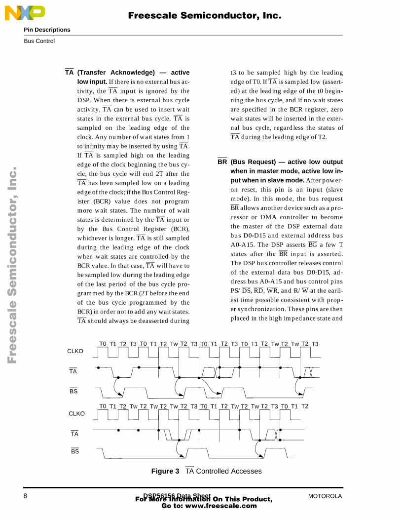
TA (Transfer Acknowledge) — activelow input. If there is no external bus ac-tivity, the TA input is ignored by theDSP. When there is external bus cycleactivity, TA can be used to insert waitstates in the external bus cycle. TA issampled on the leading edge of theclock. Any number of wait states from 1to infinity may be inserted by using TA.If TA is sampled high on the leadingedge of the clock beginning the bus cy-cle, the bus cycle will end 2T after theTA has been sampled low on a leadingedge of the clock; if the Bus Control Reg-ister (BCR) value does not programmore wait states. The number of waitstates is determined by the TA input orby the Bus Control Register (BCR),whichever is longer. TA is still sampledduring the leading edge of the clockwhen wait states are controlled by theBCR value. In that case, TA will have tobe sampled low during the leading edgeof the last period of the bus cycle pro-grammed by the BCR (2T before the endof the bus cycle programmed by theBCR) in order not to add any wait states.TA should always be deasserted during
t3 to be sampled high by the leadingedge of T0. If TA is sampled low (assert-ed) at the leading edge of the t0 begin-ning the bus cycle, and if no wait statesare specified in the BCR register, zerowait states will be inserted in the exter-nal bus cycle, regardless the status ofTA during the leading edge of T2.
BR (Bus Request) — active low outputwhen in master mode, active low in-put when in slave mode. After power-on reset, this pin is an input (slavemode). In this mode, the bus requestBR allows another device such as a pro-cessor or DMA controller to becomethe master of the DSP external databus D0-D15 and external address busA0-A15. The DSP asserts BG a few Tstates after the BR input is asserted.The DSP bus controller releases controlof the external data bus D0-D15, ad-dress bus A0-A15 and bus control pinsPS/DS, RD, WR, and R/W at the earli-est time possible consistent with prop-er synchronization. These pins are thenplaced in the high impedance state and
Bus Control
T0 T1 T2 T3 T0 T1 T2 Tw T2 T3 T0 T1 T2 T3 T0 T1 T2 Tw T2 Tw T2 T3
T0 T1 T2 Tw T2 Tw T2 Tw T2 T3 T0 T1 T2 Tw T2 Tw T2 T3 T0 T1 T2
CLKO
TA
BS
CLKO
TA
BS
Figure 3 TA Controlled Accesses
Fre
esc
ale
Se
mic
on
du
cto
r, I
Freescale Semiconductor, Inc.
For More Information On This Product, Go to: www.freescale.com
nc
...

Pin Descriptions
MOTOROLA DSP56156 Data Sheet 9
the BB pin is deasserted. The DSP con-tinues executing instructions only if in-ternal program and data memoryresources are accessed. If the DSP re-quests the external bus while BR inputpin is asserted, the DSP bus controllerinserts wait states until the external busbecomes available (BR and BB deas-serted). Note that interrupts are notserviced when a DSP instruction iswaiting for the bus controller. Notealso that BR is prevented from inter-rupting the execution of a read/ modi-fy/write instruction.
If the master bit in the OMR register isset, this pin becomes an output (MasterMode). In this mode, the DSP is not theexternal bus master and has to assertBR to request the bus mastership. TheDSP bus controller will insert waitstates until BG input is asserted andwill then begin normal bus accesses af-ter the rising of the clock which sam-pled BB high. The BR output signal willremain asserted until the DSP no long-er needs the bus. In this mode, the Re-quest Hold bit (RH) of the Bus ControlRegister (BCR) allows BR to be assertedunder software control.
During external accesses caused by aninstruction executed out of external pro-gram memory, BR remains asserted lowfor consecutive external X memory ac-cesses and continues toggling for con-secutive external P memory accessesunless the Request Hold bit (RH) is setinside the Bus Control Register (BCR).
In the master mode, BR can also beused for non arbitration purpose: if BGis always asserted, BR is asserted in t0of every external bus access. It can thenbe used as a chip select to turn a exter-
nal memory device off and on betweeninternal and external bus accesses. BRtiming is in that case similar to A0-A15,R/W and PS/DS; it is asserted anddeasserted during t0.
BG (Bus Grant) — active low input whenin master mode, active low outputwhen in slave mode. Output afterpower on reset if the slave is selected,this pin is asserted to acknowledge anexternal bus request. It indicates thatthe DSP will release control of the ex-ternal address bus A0-A15, data busD0-D15 and bus control pins when BBis deasserted. The BG output is assert-ed in response to a BR input. When theBG output is asserted and BB is deas-serted, the external address bus A0-A15,data bus D0-D15 and bus control pinsare in the high impedance state. BG as-sertion may occur in the middle of aninstruction which requires more thanone external bus cycle for execution.Note that BG assertion will not occurduring indivisible read-modify-writeinstructions (BFSET, BFCLR, BFCHG).When BR is deasserted, the BG outputis deasserted and the DSP regains con-trol of the external address bus, databus, and bus control pins when the BBpin is sampled high.
This pin becomes an input if the masterbit in the OMR register is set (MasterMode). It is asserted by an external pro-cessor when the DSP may become thebus master. The DSP can start normalexternal memory access after the BB pinhas been deasserted by the previousbus master. When BG is deasserted, theDSP will release the bus as soon as thecurrent transfer is completed. The stateof BG may be tested by testing the BS bitin the Bus Control Register. BG is ig-nored during hardware reset.
Bus Control
Fre
esc
ale
Se
mic
on
du
cto
r, I
Freescale Semiconductor, Inc.
For More Information On This Product, Go to: www.freescale.com
nc
...
10 DSP56156 Data Sheet MOTOROLA
Pin Descriptions
BB (Bus Busy) — active low input whennot bus master, active low outputwhen bus master. This pin is assertedby the DSP when it becomes the busmaster and it performs an external ac-cess. It is deasserted when the DSP re-leases bus mastership. BB becomes aninput when the DSP is no longer thebus master.
Interrupt and Mode Control MODA/IRQA (Mode Select A/External In-
terrupt Request A) — input. This in-put has two functions:
•to select the initial chip operating mode and,
•to allow an external device to request a DSP interrupt after internal syn-chronization.
MODA is read and internally latchedin the DSP when the processor exits thereset state. MODA and MODB selectthe initial chip operating mode. Severalclock cycles after leaving the reset state,the MODA pin changes to the externalinterrupt request IRQA. The chip oper-ating mode can be changed by soft-ware after reset.
The IRQA input is a synchronized ex-ternal interrupt request which indi-cates that an external device isrequesting service. It may be pro-grammed to be level sensitive or nega-tive edge triggered. If level sensitivetriggering is selected, an external pullup resistor is required for wired-ORoperation. If the processor is in the stopstandby state and IRQA is asserted, theprocessor will exit the stop state.
MODB/IRQB (Mode Select B/External In-terrupt Request B) — input. This in-put has two functions:
•to select the initial chip operating mode and,
•to allow an external device to request a DSP interrupt after internal syn-chronization.
MODB is read and internally latched inthe DSP when the processor exits thereset state. MODA and MODB selectthe initial chip operating mode. Severalclock cycles after leaving the reset state,the MODB pin changes to the externalinterrupt request IRQB. After reset, thechip operating mode can be changedby software.
The IRQB input is an external interruptrequest which indicates that an exter-nal device is requesting service. It maybe programmed to be level sensitive ornegative edge triggered. If level sensi-tive triggering is selected, an externalpull up resistor is required for wired-OR operation.
MODC (Mode Select C) — input. This inputselects the initial bus operating mode.When tied high, the external bus is pro-grammed in the master mode (BR out-put and BG input) and when tied lowthe bus is programmed in the slavemode (BR input and BG output).MODC is read and internally latched inthe DSP when the processor exits thereset state. After RESET, the bus operat-ing mode can be changed by software bywriting the MC bit of the OMR register.
RESET (Reset) — input. This input is a directhardware reset of the processor. WhenRESET is asserted, the DSP is initializedand placed in the reset state. A Schmitt
Interrupt and Mode ControlBus Control
Fre
esc
ale
Se
mic
on
du
cto
r, I
Freescale Semiconductor, Inc.
For More Information On This Product, Go to: www.freescale.com
nc
...
Pin Descriptions
MOTOROLA DSP56156 Data Sheet 11
trigger input is used for noise immunity.When the reset pin is deasserted, the ini-tial chip operating mode is latched fromthe MODA and MODB pins, and the ini-tial bus operating mode is latched fromthe MODC pin. The internal reset signalshould be deasserted synchronized withthe internal clocks.
Host Interface H0-H7 (Host Data Bus) — bidirectional. This
bidirectional data bus is used to transferdata between the host processor and theDSP. This bus is an input unless enabledby a host processor read. H0-H7 may beprogrammed as Port B general purposeparallel I/O pins called PB0-PB7 whenthe Host Interface (HI) is not being used.
HA0-HA2 (Host Address 0-2) — input*. Theseinputs provide the address selectionfor each HI register and are stablewhen HEN is asserted. HA0-HA2 maybe programmed as Port B general pur-pose parallel I/O pins called PB8-PB10when the HI is not being used.
HR/W (Host Read/Write) — input*. This in-put selects the direction of data transferfor each host processor access. If HR/Wis high and HEN is asserted, H0-H7 areoutputs and DSP data is transferred tothe host processor. If HR/W is low andHEN is asserted, H0-H7 are inputs andhost data is transferred to the DSP.When HEN is asserted, HR/W is stable.HR/W may be programmed as a gen-eral purpose I/O pin called PB11when the HI is not being used.
HEN (Host Enable) — input*. This input en-ables a data transfer on the host databus. When HEN is asserted and HR/Wis high, H0-H7 becomes an output andDSP data may be latched by the hostprocessor. When HEN is asserted andHR/W is low, H0-H7 is an input andhost data is latched inside the DSPwhen HEN is deasserted. Normally achip select signal derived from host ad-dress decoding and an enable clock isconnected to the Host Enable. HENmay be programmed as a general pur-pose I/O pin called PB12 when the HIis not being used.
HREQ (Host Request) — output*. This open-drain output signal is used by the HI torequest service from the host proces-sor. HREQ may be connected to an in-terrupt request pin of a host processor,a transfer request of a DMA controller,or a control input of external circuitry.HREQ is asserted when an enabled re-quest occurs in the HI. HREQ is deas-serted when the enabled request iscleared or masked, DMA HACK is as-serted, or the DSP is reset. HREQ maybe programmed as a general purposeI/O pin (not open-drain) called PB13when the HI is not being used.
HACK (Host Acknowledge) — input*. Thisinput has two functions:
•to provide a host acknowledge signal for DMA transfers and,
•to control handshaking and to pro-vide a host interrupt acknowledge compatible with MC68000 family processors.
If programmed as a host acknowledgesignal, HACK may be used as a datastrobe for HI DMA data transfers. If pro-grammed as an MC68000 host interrupt
Host Interface
* These pins can be bidirectional when programmed as general purpose I/O.
Interrupt and Mode Control
Fre
esc
ale
Se
mic
on
du
cto
r, I
Freescale Semiconductor, Inc.
For More Information On This Product, Go to: www.freescale.com
nc
...
12 DSP56156 Data Sheet MOTOROLA
Pin Descriptions
acknowledge, HACK enables the HIInterrupt Vector Register (IVR) ontothe host data bus H0-H7 if the Host Re-quest HREQ output is asserted. In thiscase, all other HI control pins are ig-nored and the HI state is not affected.HACK may be programmed as a gen-eral purpose I/O pin called PB14 whenthe HI is not being used.
16-bit Timer TIN (Timer Input) — input*. This input re-
ceives external pulses to be counted bythe on-chip 16-bit timer when externalclocking is selected. The pulses are in-ternally synchronized to the DSP coreinternal clock. TIN may be pro-grammed as a general purpose I/O pincalled PC10 when the external eventfunction is not being used.
TOUT (Timer Output) — output*. This out-put generates pulses or toggles on atimer overflow event or a compareevent. TOUT may be programmed as ageneral purpose I/O pin called PC11when disabled by the timer out enablebits (TO2-TO0).
Synchronous Serial Interfaces (SSI)STD0-1 (SSI0-1 Transmit Data) — output*.
These output pins transmit serial datafrom the SSI0-1 Transmit Shift Register.STD0 and STD1 may be programmedas a general purpose I/O pin called
PC0 and PC5, respectively, when theSTD function is not being used.
SRD0-1 (SSI0-1 Receive Data) — input*.These input pins receive serial data andtransfer the data to the SSI0-1 ReceiveShift Register. SRD0 and SRD1 may beprogrammed as a general purpose I/Opin called PC1 and PC6, respectively,when the SRD function is not beingused.
SCK0-1 (SSI0-1 Serial Clock) — bidirection-al. These bidirectional pins provide theserial bit rate clock for the SSI0-1 inter-face. SCK0 and SCK1 may be pro-grammed as a general purpose I/O pincalled PC2 and PC7, respectively,when the SSI0-1 interfaces are not be-ing used.
SC10-11 (SSI0-1 Serial Control 1) — bidirec-tional. These bidirectional pins areused by the SSI0-1 serial interface asframe sync I/O or flag I/O. SC10 andSC11 may be programmed as a generalpurpose I/O pin called PC3 and PC8,respectively, when the SSI0-1 are notusing these pins.
SC00-01 (SSI0-1 Serial Control 0) — bidirec-tional. These bidirectional pins areused by the SSI0-1 serial interface asframe sync I/O or flag I/O. SC00 andSC01 may be programmed as a generalpurpose I/O pin called PC4 and PC9,respectively, when the SSI0-1 are notusing these pins.
16-bit TimerSSI
* These pins can be bidirectional when programmed as general purpose I/O.
Fre
esc
ale
Se
mic
on
du
cto
r, I
Freescale Semiconductor, Inc.
For More Information On This Product, Go to: www.freescale.com
nc
...

Pin Descriptions
MOTOROLA DSP56156 Data Sheet 13
On-Chip Emulation (OnCETM Port) DSI/OS0 (Debug Serial Input/Chip Status 0) —
bidirectional. The DSI/OS0 pin, whenan input, is the pin through which seri-al data or commands are provided tothe OnCE port controller. The data re-ceived on the DSI pin will be recog-nized only when the DSP has enteredthe debug mode of operation. Datamust have valid TTL logic levels beforethe serial clock falling edge. Data is al-ways shifted into the OnCE serial portmost significant bit (MSB) first. When theDSP is not in the debug mode, the DSI/OS0 pin provides information about thechip status if it is an output and used inconjunction with the OS1 pin.
DSCK/OS1 (Debug Serial Clock/Chip Status 1)— bidirectional. The DSCK/OS1 pin,when an input, is the pin throughwhich the serial clock is supplied to theOnCE port. The serial clock providespulses required to shift data into andout of the OnCE serial port. Data isclocked into the OnCE port on the fall-ing edge and is clocked out of theOnCE serial port on the rising edge. Ifthe DSCK/OS1 pin is an output andused in conjunction with the OS0 pin, itprovides information about the chipstatus when the DSP is not in the debugmode.
DSO (Debug Serial) — output. The debugserial output provides the data con-tained in one of the OnCE port control-ler registers as specified by the lastcommand received from the commandcontroller. When idle, this pin is high.When the requested data is available, theDSO line will be asserted (negative truelogic) for four T cycles (one instruction
cycle) to indicate that the serial shift reg-ister is ready to receive clocks in order todeliver the data. When the chip entersthe debug mode due to an external de-bug request (DR), an internal softwaredebug request (DEBUG), a hardwarebreakpoint occurrence or a trace/stepoccurrence, this line will be asserted forthree T cycles to indicate that the chiphas entered the debug mode and is wait-ing for commands. Data is always shift-ed out the OnCE serial port with themost significant bit first.
DR (Debug Request) — input. The debugrequest input provides a means of en-tering the debug mode of operation.This pin, when asserted, will cause theDSP to finish the current instruction be-ing executed, enter the debug mode,and wait for commands to be enteredfrom the debug serial input line.
On-Chip Codec AUX (Auxiliary) — input. This pin is select-
ed as the analog input to the A/D con-verter when the INS bit is set in thecodec control register COCR. This pinshould be left floating when the codecis not used.
BIAS (Bias current) — input. This input isused to determine the bias current forthe analog circuitry. Connecting a re-sistor between BIAS and GNDA willprogram the current bias generator.This pin should be left floating whenthe codec is not used.
MIC (Microphone) — input. This pin is se-lected as the analog input to the A/Dconverter when the INS bit is cleared in
OnCEOn-Chip Codec
Fre
esc
ale
Se
mic
on
du
cto
r, I
Freescale Semiconductor, Inc.
For More Information On This Product, Go to: www.freescale.com
nc
...

14 DSP56156 Data Sheet MOTOROLA
Pin Descriptions
the codec control register COCR. Thispin should be left floating when the co-dec is not used.
SPKP (Speaker Plus) — output. This pin isthe positive analog output from the on-chip D/A converter. This pin should beleft floating when the codec is not used.
SPKM (Speaker Minus) — output. This pin isthe negative analog output from theon-chip D/A converter. This pinshould be left floating when the codecis not used.
VREF (Voltage Reference) — output. Thispin is the op-amp buffer output in thereference voltage generator. It has avalue of (2/5)VCCA. This pin should al-ways be connected to the GNDAthrough two capacitors, even when thecodec is not used.
VDIV (Voltage Division) — output. Thisoutput pin is also the output to the on-chip op-amp buffer in the referencevoltage generator. It is connected to aresistor divider network located withinthe codec block which provides a volt-age equal to (2/5)VCCA. This pin shouldbe connected to the GND via a capacitorwhen the codec is used and should beleft floating when the codec is not used.
Power, Ground, and Clock VCC (Power) — Power pins
GND (Ground) — Ground pins
VCCS (Synthesizer Power) — This pin sup-
plies a quiet power source to the Phase-Locked Loop (PLL) to provide greaterfrequency stability.
GNDS (Synthesizer Ground) — This pin sup-plies a quiet ground source to the PLLto provide greater frequency stability.
VCCA (Analog Power) — This pin is the posi-
tive analog supply input. It should be con-nected to VCC when the codec is not used.
GNDA (Analog Ground) — This pin is the an-alog ground return. It should be con-nected to digital GND when the codecis not used.
EXTAL (External Clock) — input. This inputshould be driven by an external clock orby an external oscillator. After beingsquared, the input frequency can beused as the DSP core internal clock. Inthat case, it is divided by two to producea four phase instruction cycle clock, theminimum instruction time being two in-put clock periods. This input frequencyis also used, after division, as inputclock for the on-chip codec and the on-chip PLL.
CLKO (Clock Output) — output. This pinoutputs a buffered clock signal. By pro-gramming two bits (CS1-CS0) insidethe PLL Control Register (PLCR), theuser can select between outputting asquared version of the signal applied toEXTAL, a squared version of the signalapplied to EXTAL divided by 2, and adelayed version of the DSP core masterclock. The clock frequency on this pincan be disabled by setting the ClockoutDisable bit (CD; bit 7) of the OperatingMode Register (OMR). When disabled,the pin can be left floating.
SXFC (External Filter Capacitor) — This pinadds an external capacitor to the PLLfilter circuit. A low leakage capacitorshould be connected between and lo-cated very close to SXFC and VCCS.
Power, Ground, and ClockOn-Chip Codec
Fre
esc
ale
Se
mic
on
du
cto
r, I
Freescale Semiconductor, Inc.
For More Information On This Product, Go to: www.freescale.com
nc
...
Electrical Characteristics and Timing
MOTOROLA DSP56156 Data Sheet 15
Electrical Characteristics and Timing
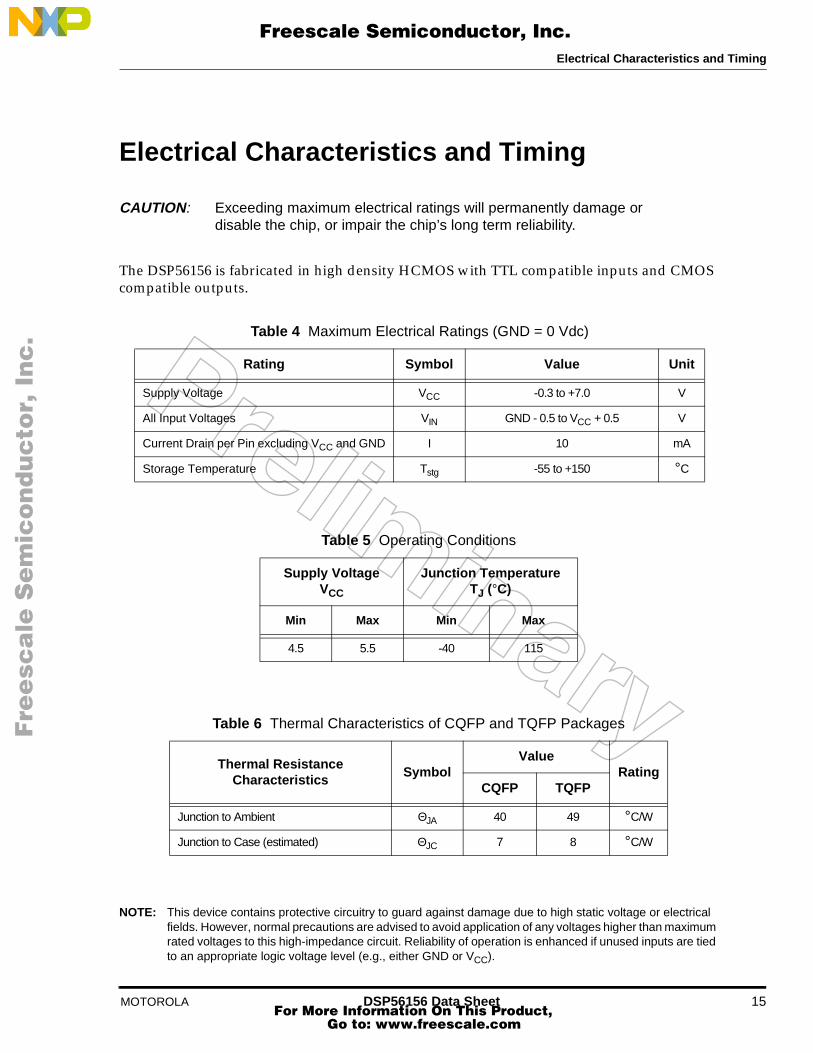
CAUTION: Exceeding maximum electrical ratings will permanently damage or disable the chip, or impair the chip’s long term reliability.
The DSP56156 is fabricated in high density HCMOS with TTL compatible inputs and CMOS compatible outputs.
NOTE: This device contains protective circuitry to guard against damage due to high static voltage or electrical fields. However, normal precautions are advised to avoid application of any voltages higher than maximum rated voltages to this high-impedance circuit. Reliability of operation is enhanced if unused inputs are tied to an appropriate logic voltage level (e.g., either GND or VCC).
Table 4 Maximum Electrical Ratings (GND = 0 Vdc)
Rating Symbol Value Unit
Supply Voltage VCC -0.3 to +7.0 V
All Input Voltages VIN GND - 0.5 to VCC + 0.5 V
Current Drain per Pin excluding VCC and GND I 10 mA
Storage Temperature Tstg -55 to +150 °C
Table 5 Operating Conditions
Supply VoltageVCC
Junction TemperatureTJ (°C)
Min Max Min Max
4.5 5.5 -40 115
Table 6 Thermal Characteristics of CQFP and TQFP Packages
Thermal Resistance Characteristics
SymbolValue
RatingCQFP TQFP
Junction to Ambient ΘJA 40 49 °C/W
Junction to Case (estimated) ΘJC 7 8 °C/W
Fre
esc
ale
Se
mic
on
du
cto
r, I
Freescale Semiconductor, Inc.
For More Information On This Product, Go to: www.freescale.com
nc
...

Electrical Characteristics and Timing
16 DSP56156 Data Sheet MOTOROLA
Analog I/O Characteristics(VCCA = 5.0 V dc ± 10%, TJ = -40° to +125°C)
The analog I/O characteristics of this device are listed in Table 7. For additional information regarding the use of analog signals, see “Design Considerations” at the end of this document.
Table 7 Analog I/O Characteristics
Characteristic Min Typ Max Unit
Input Impedance on MIC and AUX (See Note 1) 46 78 1400 kΩ
Input Capacitance on MIC and AUX — — 10 pF
Peak Input Voltage on the MIC/AUX Input for Full Scale Linearity (0.14 dBm0): 6 dB - MGS1 - 0 = 00(See Note 2) 0 dB - MGS1 - 0 = 01
6 dB - MGS1 - 0 = 1017 dB - MGS1 - 0 = 11
————
————
1.4140.707354100
VpVp
mVpmVp
Internal Input Gain Variation;G = -6 dB, 0 dB, 6 dB or 17 dB(±0.83 dB variation due to 10% variation on VCC):
G - 0.83 G G + 0.83 dB
VREF Output Voltage 1.8 2 2.2 V
VREF Output Current — — ±1 mA
DC Offset Between SPKP and SPKM — — 100 mV
Allowable Differential Load Capacitance onSPKP and SPKM (with 1 kΩ in series)
0 — 0.05 µF
Allowable Single-ended Load Capacitance on SPKP or SPKM (with 0.5 kΩ in series)
0 (See Note 3)
— 1000.1
µF
Maximum Single-ended Signal Output Level — — 1 Vp
Maximum Differential Signal Output Level — — 2 Vp
Single-ended Load Resistance 500 — — Ω
Differential Load Resistance 1 — — kΩ
Resistance BIAS — 10 (See
Note 4)
— kΩ
Internal Output Volume Control VariationVC = -20, -15, -10, -5, 0, 6, 12, 18, 24, 30, 35 dB(± 0.83 dB variation due to 10% variation on VCC)
VC - 0.83 VC VC + 0.83 dB
NOTES: 1. Minimum value reached for a Codec clock of 3 MHz, typical for 2 MHz and maximum for 100 kHz2. 0 dBm0 corresponds to 3.14 dB below the input saturation level3. AC coupling is necessary in single-ended mode when the load resistor is not tied to VREF4. ± 10%
Analog I/O Characteristics
Fre
esc
ale
Se
mic
on
du
cto
r, I
Freescale Semiconductor, Inc.
For More Information On This Product, Go to: www.freescale.com
nc
...

Electrical Characteristics and Timing
MOTOROLA DSP56156 Data Sheet 17
A/D and D/A Performance(VCCA = 5.0 V dc ± 10%, TJ = -40° to +125°C)
The A/D and D/A performance of the codec section are given in Table 8 with an example presented in Figure 4.
NOTES: 1. 0 dB gain on the A/D and D/A; Codec clock at 1.538 MHz with 128 decimation/interpolation ratio and tested at 1502 Hz
2. 0 dBm0 corresponds to -3.14 dB below the input saturation level
Figure 4 Example: S/N and S/N+T Performance for the A/D Section
Table 8 A/D and D/A Performance of Codec
Characteristic Level Min Typ
(See Note 1)Max Unit
Analog to Digital Section Signal to Noise plus Distortion Ratio (S/N+T)
0 dBm0(See Note 2)
55 65 — dB
-50 dBm0 15 20 — dB
Digital to Analog Section Signal to Noise plus Distortion Ratio (S/N+T)
0 dB 55 65 — dB
-50 dB 15 20 — dB
S in dB
0
10
20
30
40
50
60
70
80S/N
S/N+T
Signal in dB
÷13
CODEC
÷(12+1)*4
2 MHz
1 MHz
PLL52 MHz
COCR=$E400
PLL
Codec
÷(12+1)x4
÷ 13
÷ 6.5
13 MHz
A/D and D/A Performance
Fre
esc
ale
Se
mic
on
du
cto
r, I
Freescale Semiconductor, Inc.
For More Information On This Product, Go to: www.freescale.com
nc
...

Electrical Characteristics and Timing
18 DSP56156 Data Sheet MOTOROLA
Other On-Chip Codec Characteristics(VCCA = 5.0 V dc ± 10%, TJ = -40° to +125°C, CL = 50 pF + 1 TTL Load)
The analog I/O characteristics of this device are shown in Table 9.
Table 9 Analog I/O Characteristics of On-Chip Codec
Characteristic Min Typ Max Unit
Codec Master Clock 0.1 2.048 3 MHz
Codec Sampling Rate 78 16000 37000 Hz
A/D Section Group Delay — — 0.2 msec
D/A Section Group Delay — — 0.2 msec
Other On-Chip Codec Characteristics
Fre
esc
ale
Se
mic
on
du
cto
r, I
Freescale Semiconductor, Inc.
For More Information On This Product, Go to: www.freescale.com
nc
...
DC Electrical Characteristics and Timing
MOTOROLA DSP56156 Data Sheet 19
DC Electrical Characteristics (GND = 0 V dc)
(VCC = 5.0 V dc ± 10%, TJ = -40° to +125°C, CL = 50 pF + 1 TTL Load)
The DC electrical characteristics of this device are shown in Table 10.
NOTES: 1. When EXTAL is AC coupled, VIHC - VILC Š 1 V must be true. 2. Input capacitance is periodically sampled and not 100% tested in production.
Table 10 DC Electrical Characteristics
Characteristic Symbol Min Typ Max Unit
Input High Voltage except EXTAL, RESET, MODA, MODB, MODC
VIH 2.0 — VCC V
Input Low Voltage except EXTAL, MODA, MODB, MODC
VIL -0.5 — 0.8 V
Input High Voltage EXTAL DC coupledEXTAL AC coupled (See Note 1)
VIHC70% of VCC
1——
VCCVCC
V
Input Low Voltage EXTAL DC coupledEXTAL AC coupled (See Note 1)
VILC-0.5-0.5
——
20% of VCCVCC-1
V
Input High Voltage RESET VIHR 2.5 — VCC V
Input High Voltage MODA, MODB, MODC VIHM 3.5 — VCC V
Input Low Voltage MODA, MODB, MODC VILM -0.5 — 2.0 V
Input Leakage CurrentEXTAL
RESET, MODA, MODB, MODC, TA, DR, BR
IIN-100
-1
—100
1µAµA
Three-State (Off-State) Input Current (@2.4 V/0.5 V)
TSI -10 — 10 µA
Output High Voltage (IOH = -10 µA) VOHC VCC -0.1 — — V
Output High Voltage (IOH = -0.4 mA) VOH 2.4 — — V
Output Low Voltage (IOL = 10 µA) VOLC — — 0.1 V
Output Low Voltage (IOL = 3.2 mAR/W IOL = 1.6 mA; Open DrainHREQ IOL = 6.7 mA, TXD IOL = 6.7 mA)
VOL — — 0.4 V
Input Capacitance (See Note 2) CIN — 10 — pF
Fre
esc
ale
Se
mic
on
du
cto
r, I
Freescale Semiconductor, Inc.
For More Information On This Product, Go to: www.freescale.com
nc
...
AC Electrical Characteristics and Timing
20 DSP56156 Data Sheet MOTOROLA
AC Electrical Characteristics (GND = 0 V dc)
The timing waveforms in the AC Electrical Characteristics are tested with a VIL maximum of 0.5 V and a VIH minimum of 2.4 V for all pins, except EXTAL, RESET, MODA, MODB and MODC. These five pins are tested using the input levels set forth in the DC Electrical Charac-teristics. AC timing specifications which are referenced to a device input signal are measured in production with respect to the 50% point of the respective input signal’s transition. The DSP56156 output levels are measured with the production test machine VOL and VOH refer-ence levels set at 0.8 V and 2.0 V respectively.
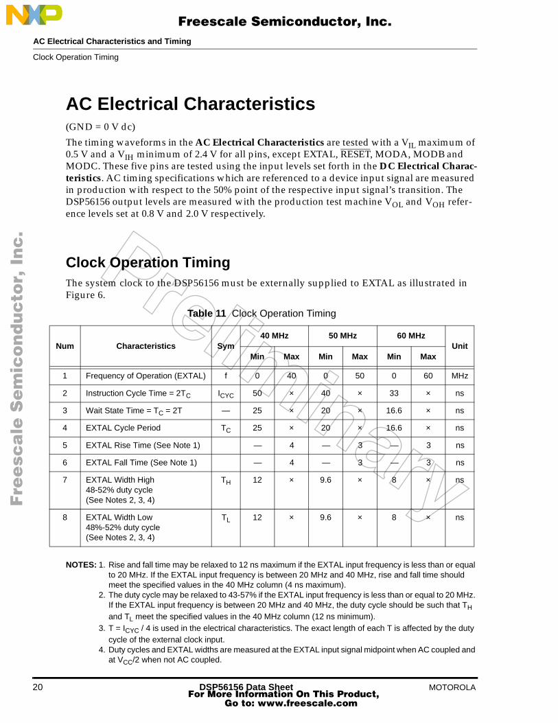
Clock Operation TimingThe system clock to the DSP56156 must be externally supplied to EXTAL as illustrated in Figure 6.
NOTES: 1. Rise and fall time may be relaxed to 12 ns maximum if the EXTAL input frequency is less than or equal to 20 MHz. If the EXTAL input frequency is between 20 MHz and 40 MHz, rise and fall time should meet the specified values in the 40 MHz column (4 ns maximum).
2. The duty cycle may be relaxed to 43-57% if the EXTAL input frequency is less than or equal to 20 MHz. If the EXTAL input frequency is between 20 MHz and 40 MHz, the duty cycle should be such that TH and TL meet the specified values in the 40 MHz column (12 ns minimum).
3. T = ICYC / 4 is used in the electrical characteristics. The exact length of each T is affected by the duty cycle of the external clock input.
4. Duty cycles and EXTAL widths are measured at the EXTAL input signal midpoint when AC coupled and at VCC/2 when not AC coupled.
Table 11 Clock Operation Timing
Num Characteristics Sym40 MHz 50 MHz 60 MHz
UnitMin Max Min Max Min Max
1 Frequency of Operation (EXTAL) f 0 40 0 50 0 60 MHz
2 Instruction Cycle Time = 2TC ICYC 50 × 40 × 33 × ns
3 Wait State Time = TC = 2T — 25 × 20 × 16.6 × ns
4 EXTAL Cycle Period TC 25 × 20 × 16.6 × ns
5 EXTAL Rise Time (See Note 1) — 4 — 3 — 3 ns
6 EXTAL Fall Time (See Note 1) — 4 — 3 — 3 ns
7 EXTAL Width High 48-52% duty cycle (See Notes 2, 3, 4)
TH 12 × 9.6 × 8 × ns
8 EXTAL Width Low 48%-52% duty cycle(See Notes 2, 3, 4)
TL 12 × 9.6 × 8 × ns
Clock Operation Timing
Fre
esc
ale
Se
mic
on
du
cto
r, I
Freescale Semiconductor, Inc.
For More Information On This Product, Go to: www.freescale.com
nc
...

AC Electrical Characteristics and Timing
MOTOROLA DSP56156 Data Sheet 21
Figure 5 External Clock Timing
Other Clock and PLL Operation TimingClock and PLL timings are listed in Table 12 and the clocking configurations are illustrated in Figure 6.
Figure 6 Clocking Configurations
EXTAL
VIHC
Midpoint
7 8
4
2
56
TH TL
90%
10%VILC
Table 12 Clock and PLL Timing
Characteristics Min Max Unit
PLL Output frequency 10 Max Fosc(See Note 1)
MHz
EXTAL Input Clock Amplitude (See Note 2) 1 VCC Vpp
NOTES: 1. Maximum DSP operating frequency. See Table 11.2. An AC coupling capacitor is required on EXTAL if the levels are out of the normal CMOS level
range (VILC>20% of VCC or VIHC<70% of VCC).
EXTAL
PLL
PLLE=1
PLLE=0
FoscED3-ED0
CLKO ÷ 2internal phase PH0 at Fosc
CS1-CS0
1000 pF
GSM
SXFC VCCS
XFC
0.01 µF
GNDS
0.1 µF
100 KΩ÷ 1 to ÷ 16
÷ 6.5
CODEC
VCOLF
PFD
YD3-YD0
÷ 1 to ÷ 16
10 nF
÷ 4
Clock Operation TimingPLL
Fre
esc
ale
Se
mic
on
du
cto
r, I
Freescale Semiconductor, Inc.
For More Information On This Product, Go to: www.freescale.com
nc
...

AC Electrical Characteristics and Timing
22 DSP56156 Data Sheet MOTOROLA
Reset, Stop, Wait, Mode Select, and Interrupt Timing(VCC = 5.0 V dc ± 10%, TJ = -40° to +125°C, CL = 50 pF + 1 TTL Load)
cyc = Clock cycle = 1/2 instruction cycle = 2 T cycles ws = Number of wait states programmed into external bus access using BCR (WS = 0 - 31)
Table 13 Reset, Stop, Wait, Mode Select, and Interrupt Timing
Num Characteristics40 MHz 50 MHz 60 MHz
UnitMin Max Min Max Min Max
10 RESET Assertion to Address, Data and Control Signals High Impedance
— 25 — 23 — 21 ns
11 Minimum Stabilization Duration (See Note 1) OMR bit 6=0
OMR bit 6=1600KT
60T——
600KT60T
——
600KT60T
——
nsns
12 Asynchronous RESET Deassertion to First External Address Output (See Note 7)
16T 18T+20 16T 18T+17 16T 18T+15 ns
13 Synchronous Reset Setup Time from RESET Deassertion to Rising Edge of CLKO
7 cyc-4 6 cyc-3 5 cyc-2 ns
14 Synchronous Reset Delay Time from CLKO High to the First External Access (See Note 7)
16T+3 16T+20 16T+ 3 16T+18 16T+3 16T+16 ns
15 Mode Select Setup Time 22 — 20 — 18 — ns
16 Mode Select Hold Time 0 — 0 — 0 — ns
17 Edge-triggered Interrupt Request Width 13 — 11 — 9 — ns
18 Delay from IRQA, IRQB Assertion to External Data Memory Access Out Valid - Caused by First Interrupt
Instruction Fetch- Caused by First Interrupt
Instruction Execution
11T+4
19T+4
—
—
11T+4
19T+4
—
—
11T+3
19T+3
—
—
ns
ns
19 Delay from IRQA, IRQB Assertion to General Purpose Output Valid Caused by the Execution of the First Interrupt Instruction
22T+5—
22T+4 — 22T+3 — ns
20 Delay from External Data Memory Address Output Valid Caused by First Interrupt Instruction Execution to Inter-rupt Request Deassertion for Level Sen-sitive Fast Interrupts (See Note 2)
— 5T-26+
cyc × ws
— 5T-24+
cyc × ws
— 5T-22+
cyc × ws
ns
Reset, Stop, Wait, Mode Select, and Interrupt Timing
Fre
esc
ale
Se
mic
on
du
cto
r, I
Freescale Semiconductor, Inc.
For More Information On This Product, Go to: www.freescale.com
nc
...

AC Electrical Characteristics and Timing
MOTOROLA DSP56156 Data Sheet 23
(VCC = 5.0 V dc ± 10%, TJ = -40° to +125°C, CL = 50 pF + 1 TTL Load)
Table 13 Reset, Stop, Wait, Mode Select, and Interrupt Timing (continued)
Num Characteristics40 MHz 50 MHz 60 MHz
UnitMin Max Min Max Min Max
21 Delay from General-Purpose Output Valid Caused by the Execution of the First Inter-rupt Instruction to IRQA, IRQB Deassertion for Level Sensitive Fast Interrupts — If 2nd Interrupt Instruction is:
Single Cycle(See Note 2)
Two Cycles
—
—
cyc - 29
3 cyc - 29
—
—
cyc - 27
3 cyc - 27
—
—
cyc - 26
3 cyc - 26
ns
ns
22 Synchronous setup time from IRQA, IRQB assertion to Synchronous falling edge of CLKO (See Notes 5 and 6)
14 cyc-3 13 cyc-2 12 cyc-1 ns
23 Falling Edge of CLKO to First Interrupt Vector Address Out Valid after Synchronous recovery from Wait State (See Notes 3 and 5)
27T+3 27T+20 27T+3 27T+18 27T+3 27T+16 ns
24 IRQA Width Assertion to Recover from Stop State (See Note 4)
15 — 13 — 12 — ns
25 Delay from IRQA Assertion to Fetch of first instruction (exit-ing Stop) (See Notes 1 and 3) OMR bit 6=0
OMR bit 6=1524303T+4
47T+4——
524303T+3 47T+3
——
524303T+3 47T+3
——
nsns
28 Duration for Level Sensitive IRQA Assertion to Cause the Fetch of First IRQA Interrupt Instruction (exiting Stop)(See Notes 1 and 3)
OMR bit 6=0OMR bit 6=1
524303T47T
——
524303T47T
——
524303T47T
——
nsns
29 Delay from Level Sensitive IRQA Assertion to First Inter-rupt Vector Address Out Valid (exiting Stop)(See Notes 1 and 3)
OMR bit 6=0OMR bit 6=1
524303T+4 47T+4
——
524303T+3 47T+3
——
524303T+3 47T+3
——
nsns
Reset, Stop, Wait, Mode Select, and Interrupt Timing
Fre
esc
ale
Se
mic
on
du
cto
r, I
Freescale Semiconductor, Inc.
For More Information On This Product, Go to: www.freescale.com
nc
...

AC Electrical Characteristics and Timing
24 DSP56156 Data Sheet MOTOROLA
NOTES: 1. Circuit stabilization delay is required during reset when using an external clock in two cases:• after power-on reset• when recovering from Stop mode
2. When using fast interrupts, IRQA or IRQB is defined as level-sensitive, then timings 20 and 21 apply to prevent multiple interrupt service. To avoid these timing restrictions, the negative edge-trig-gered mode is recommended when using fast interrupts.
3. The interrupt instruction fetch is visible on the pins only in Mode 3.4. The minimum is specified for the duration of an edge triggered IRQA interrupt required to recover
from the Stop state. This is not the minimum required so that the IRQA interrupt is accepted.5. Timing #22 is for all IRQx interrupts while timing #23 is only when exiting the Wait state.6. Timing #22 triggers off T1 in the normal state and off phi1 when exiting the Wait state.7. The instruction fetch is visible on the pins only in Mode 2 and Mode 3.
Figure 7 Asynchronous Reset Timing
Figure 8 Synchronous Reset Timing
RESET
D0-D15A0-A15
PS/DSR/W
BS
10
11 12
First Fetch
VIHR
CLKO
RESET
A0-A15PS/DS
BSR/W
14
13
Reset, Stop, Wait, Mode Select, and Interrupt Timing
Fre
esc
ale
Se
mic
on
du
cto
r, I
Freescale Semiconductor, Inc.
For More Information On This Product, Go to: www.freescale.com
nc
...
AC Electrical Characteristics and Timing
MOTOROLA DSP56156 Data Sheet 25
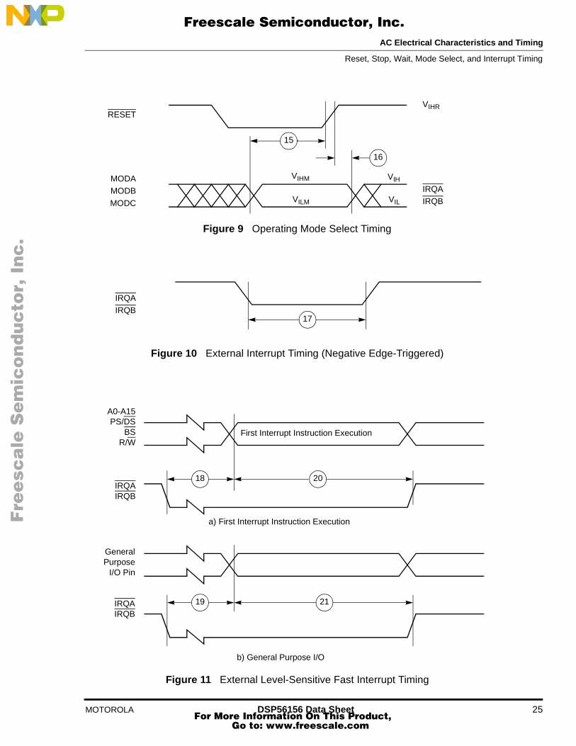
Figure 9 Operating Mode Select Timing
Figure 10 External Interrupt Timing (Negative Edge-Triggered)
Figure 11 External Level-Sensitive Fast Interrupt Timing
RESET
MODAMODB
MODC
VIHR
IRQAIRQB
VIHM
VILM
VIH
VIL
16
15
IRQAIRQB
17
First Interrupt Instruction Execution
A0-A15PS/DS
BSR/W
IRQAIRQB
2018
a) First Interrupt Instruction Execution
GeneralPurpose
I/O Pin
IRQAIRQB
19 21
b) General Purpose I/O
Reset, Stop, Wait, Mode Select, and Interrupt Timing
Fre
esc
ale
Se
mic
on
du
cto
r, I
Freescale Semiconductor, Inc.
For More Information On This Product, Go to: www.freescale.com
nc
...

AC Electrical Characteristics and Timing
26 DSP56156 Data Sheet MOTOROLA
Figure 12 Synchronous Interrupt from Wait State Timing
Figure 13 Recovery from Stop State Using Asynchronous Interrupt Timing
Figure 14 Recovery from Stop State Using IRQA Interrupt Service
22
23
T0, T2phi0
T1, T3
phi1CLKO
IRQAIRQB
A0-A15PD/DS
BSR/W
Instruction FetchFirst Interrupt
IRQA
A0-A15
PD/DSBS
R/W
24
25
Not IRQA Interrupt VectorFirst Instruction Fetch
IRQA
A0-A15PD/DS
BSR/W
First IRQA InterruptInstruction Fetch
28
29
Reset, Stop, Wait, Mode Select, and Interrupt Timing
Fre
esc
ale
Se
mic
on
du
cto
r, I
Freescale Semiconductor, Inc.
For More Information On This Product, Go to: www.freescale.com
nc
...
AC Electrical Characteristics and Timing
MOTOROLA DSP56156 Data Sheet 27
Table 14 Wait and Stop Timings
Num Characteristics40 MHz 50 MHz 60 MHz
UnitMin Max Min Max Min Max
30 DR Asserted to CLK high (Setup Time for Synchronous Recovery from Wait State)
10 cyc - 4 9 cyc - 3 8 cyc - 2 ns
31 CLK high to DSO (ACK) Valid (Enter Debug Mode) after Syn-chronous Recovery from Wait State
18 cyc — 18 cyc — 18 cyc — ns
32 DR to DSO (ACK) Valid(Enter Debug Mode)- After Asynchronous Recovery
from Stop State- After Asynchronous Recovery
from Wait State
29 cyc
18 cyc
—
—
29 cyc
18 cyc
—
—
29 cyc
18 cyc
—
—
ns
ns
33 DR Assertion Width- to Recover from Wait/Stop
without entering debug mode- to Recover from Wait/Stop
short wake-up and enter debug mode
- to Recover from Stop long wake-up and enter debug mode
12
29 cyc
262157cyc
10 cyc
—
—
11
29 cyc
262157cyc
10 cyc
—
—
10
29 cyc
262157cyc
10 cyc
—
—
ns
ns
ns
Figure 15 Recovery from Wait State Using DR Pin — Synchronous Timing
DR(input)
DSO(output)
33
32
33
Reset, Stop, Wait, Mode Select, and Interrupt Timing
Fre
esc
ale
Se
mic
on
du
cto
r, I
Freescale Semiconductor, Inc.
For More Information On This Product, Go to: www.freescale.com
nc
...

AC Electrical Characteristics and Timing
28 DSP56156 Data Sheet MOTOROLA
Figure 16 Recovery from Wait/Stop State Using DR Pin — Asynchronous Timing
Capacitance Derating The DSP56156 External Bus Timing Specifications are designed and tested at the maximum ca-pacitive load of 50 pF, including stray capacitance. Typically, the drive capability of the Exter-nal Bus pins (A0-A15, D0-D15, PS/DS, RD, BS, WR, R/W) derates linearly at 1 ns per 12 pF of additional capacitance from 50 pF to 250 pF of loading. Port B and C pins derate linearly at 1 ns per 5 pF of additional capacitance from 50 pF to 250 pF of loading.
When an internal memory access follows an external memory access, the PS/DS, R/W, RD and WR strobes remain deasserted and A0-A15 do not change from their previous state.
CLKO(output)
DR(input)
DSO(output)
31
T1, T3
30
33
T0, T2
Reset, Stop, Wait, Mode Select, and Interrupt Timing
Capacitance Derating
Fre
esc
ale
Se
mic
on
du
cto
r, I
Freescale Semiconductor, Inc.
For More Information On This Product, Go to: www.freescale.com
nc
...

AC Electrical Characteristics and Timing
MOTOROLA DSP56156 Data Sheet 29
External Bus Synchronous Timing(VCC = 5.0 V dc ± 10%, TJ = -40° to +125°C, CL = 50 pF + 1 TTL Load)
Table 15 lists external bus synchronous timing. Figure 17 and illustrate the bus timings with no wait states and two wait states, respectively.
Table 15 External Bus Synchronous Timing
Num Characteristic40 MHz 50 MHz 60 MHz
UnitMin Max Min Max Min Max
34 EXTAL CLK In High to CLKO High 2.4 9 2.4 9 2.4 9 ns
35 CLKO High to a. A0-A15 Valid
b. PS/DS, R/W Valid, BS, RD Asserted
4.7
4.7
12
14
4.7
4.7
12
14
4.7
4.7
12(See Note)
4
ns
ns
36 BS Width Deasserted 18.3 — 13.4 — 9.8 — ns
37 CLKO High to WR Asserted Low T+3.1 T+12.4 T+3.1 T+12.4 T+3.1 T+12.4 ns
38 WR and RD Deasserted High to BS Asserted Low (2 Successive Bus Cycles)
14.3 15.8 11.8 13.3 10.2 11.8 ns
39 <intentionally blank>
40 CLKO High to BS Deasserted 2.6 10.3 2.6 10.3 2.6 10.3 ns
41 TA Valid to CLKO High (Setup) 4.5 — 4.5 — 4.5 — ns
42 CLKO High to TA Invalid (Hold) 0 — 0 — 0 — ns
43 CLKO High to D0-D15 Out Valid 1.7 7.1 1.7 7.1 1.7 7.1 ns
44 CLKO High to D0-D15 Out Invalid 2.0 — 2.0 — 2.0 — ns
45 D0-D15 In Valid to CLKO Low (Setup) 6 — 6 — 6 — ns
46 CLKO Low to D0-D15 In Invalid (Hold) 0 — 0 — 0 — ns
47 CLKO Low to WR, RD Deasserted — 10 — 10 — 10 ns
48 WR, RD Hold Time from CLKO Low 2.2 — 2.2 — 2.2 — ns
49 CLKO High to D0-D15 Three-state 0 6 0 6 0 6 ns
50 CLKO High to D0-D15 Out Active 1.2 4.2 1.2 4.2 1.2 4.2 ns
51 CLKO High to A0-A15, PS/DS, R/W Invalid 2.8 — 2.8 — 2.8 — ns
NOTE: 10 ns CL = 25 pF
External Bus Synchronous Timing
Fre
esc
ale
Se
mic
on
du
cto
r, I
Freescale Semiconductor, Inc.
For More Information On This Product, Go to: www.freescale.com
nc
...

AC Electrical Characteristics and Timing
30 DSP56156 Data Sheet MOTOROLA
NOTE: During Read-Modify-Write instructions and internal instructions, the address lines do not change state.
Figure 17 External Bus Synchronous Timing — No Wait States
EXTAL(Input)
T0 T1 T2 T3 T0 T1 T2
Data In
37
35
35
41
43
Data Out
34
36
40
42
47
48
51
50
46
49
45
47
48
CLKO(Output)
A0-A15PS/DS
R/W(See Note)
BS(Output)
WR(Output)
RD(Output)
TA(Input)
D0-D15(Output)
D0-D15(Input)
41
35
44
External Bus Synchronous Timing
Fre
esc
ale
Se
mic
on
du
cto
r, I
Freescale Semiconductor, Inc.
For More Information On This Product, Go to: www.freescale.com
nc
...
AC Electrical Characteristics and Timing
MOTOROLA DSP56156 Data Sheet 31
Figure 18 External Bus Synchronous Timing – Two Wait States
EXTAL(Input)
T0 T1 T2 Tw T2 Tw T2 T3 T0
Data In
37
35
41
43
44
Data Out
34
36
40
42
47
48
51
50
46
49
45
35
47
48
4241
CLKO(Output)
A0-A15,PS/DS, R/W
(Outputs)
BS(Output)
WR(Output)
RD(Output)
TA(Input)
D0-D15(Output)
D0-D15(Input)
35
External Bus Synchronous Timing
Fre
esc
ale
Se
mic
on
du
cto
r, I
Freescale Semiconductor, Inc.
For More Information On This Product, Go to: www.freescale.com
nc
...

AC Electrical Characteristics and Timing
32 DSP56156 Data Sheet MOTOROLA
External Bus Asynchronous Timing (VCC = 5.0 V dc ± 10%, TJ = -40° to +125°C, CL = 50 pF + 1 TTL Load)
cyc = Clock cycle = 1/2 instruction cycle = 2 T cycles WS = Number of Wait States, Determined by BCR Register (WS = 0 to 31) WT = WS × cyc = 2T × WS
External Bus Asynchronous Timing
Fre
esc
ale
Se
mic
on
du
cto
r, I
Freescale Semiconductor, Inc.
For More Information On This Product, Go to: www.freescale.com
nc
...

AC Electrical Characteristics and Timing
MOTOROLA DSP56156 Data Sheet 33
Figure 19 External Bus Asynchronous Timing
Data In
64
59
Data Out
62 67
68 54 66 69
58 57
63
65
61
55
A0-A15,PS/DS, R/W
(See Note)
53
60
56
BS
WR
D0-D15
RD
52
NOTE: During Read-Modify-Write instructions and internal instructions, the address lines do not change state.
External Bus Asynchronous Timing
Fre
esc
ale
Se
mic
on
du
cto
r, I
Freescale Semiconductor, Inc.
For More Information On This Product, Go to: www.freescale.com
nc
...

AC Electrical Characteristics and Timing
34 DSP56156 Data Sheet MOTOROLA
Bus Arbitration Timing — Slave Mode(VCC = 5.0 V dc ± 10%, TJ = -40° to +125°C, CL = 50 pF + 1 TTL Load)
cyc = Clock cycle = 1/2 instruction cycle = 2 T cyclesWS = Number of Wait States for external X or P memory, Determined by BCR
Register (WS = 0 to 31)WT = WS × cyc=2T × WSWX = Number of Wait States for external X memory, Determined by BCR
Register (WS = 0 to 31)WP = Number of Wait States for external P memory, Determined by BCR
Register (WS = 0 to 31)
NOTES: 1. With no external access from the DSP561562. During external read or write access3. During external read-modify-write access4. During Stop mode — external bus is released and BG is always low5. During Wait mode6. With external accesses pending by the DSP561567. Slave mode, when bus is still busy after bus request has been deasserted
Table 17 Slave Mode
Num Characteristics40/50/60 MHz
UnitMin Max
70 BR Input to CLKO low setup time 0 1 ns
71 Delay from BR Input Assertion to (See Note 1) BG Output Assertion (See Note 2)
(See Note 3)
(See Note 4)(See Note 5)
5T+1.93T+1.95T+1.9
NAT+1.9
9T+4.26T+WT+4.2
26T+4T x WX +2T x WP+4.2
NA3T+4.2
ns
72 CLKO high to BG Output Assertion 1.9 5.2 ns
73 BG Output Deassertion Duration (See Note 1)(See Note 5)(See Note 6)
5T-0.52T-0.53T-0.5
———
ns
74 CLKO High to Control Bus High Impedance 2.7 6.5 ns
75 CLKO High to BB Output Deassertion 3.2 7.8 ns
76 CLKO High to BB Input 3.3 8.1 ns
77 BR Input Deassertion to (See Note 1)BG Output Deassertion (See Note 5)
(See Note 7)
4T+2.53T+3.23T+3.2
9T+6.48T+7.88T+8.0
ns
78 CLKO Low to BG Deassertion (See Note 1)CLKO High to BG Deassertion (See Note 5)CLKO High to BG Deassertion (See Note 7)
2.53.23.2
6.47.88.0
ns
79 CLKO High to BB Output Active 1.3 3.6 ns
80 CLKO High to BB Output Assertion 2.3 5 ns
81 CLKO High to Address and Control Bus Active 1 3 ns
82 CLKO High to Address and Control Bus Valid 2 4.4 ns
Bus Arbitration Timing — Slave Mode
Fre
esc
ale
Se
mic
on
du
cto
r, I
Freescale Semiconductor, Inc.
For More Information On This Product, Go to: www.freescale.com
nc
...

AC Electrical Characteristics and Timing
MOTOROLA DSP56156 Data Sheet 35
Figure 20 Bus Arbitration Timing — Slave Mode — Bus Release
72
74
70
71
74
76
75
73
CLKO
(Output)
BR
(Input)
BG(Output)
BB(I/O)
A0-A15PS/DS
R/W
D0-D15
Bus Arbitration Timing — Slave Mode
Fre
esc
ale
Se
mic
on
du
cto
r, I
Freescale Semiconductor, Inc.
For More Information On This Product, Go to: www.freescale.com
nc
...
AC Electrical Characteristics and Timing
36 DSP56156 Data Sheet MOTOROLA
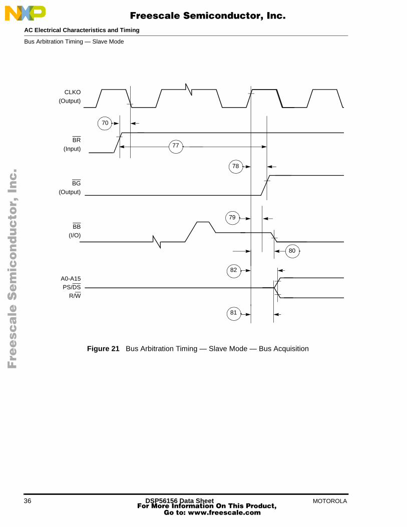
Figure 21 Bus Arbitration Timing — Slave Mode — Bus Acquisition
70
78
80
79
77
81
82
CLKO
(Output)
BR
(Input)
BG(Output)
BB(I/O)
A0-A15PS/DS
R/W
Bus Arbitration Timing — Slave Mode
Fre
esc
ale
Se
mic
on
du
cto
r, I
Freescale Semiconductor, Inc.
For More Information On This Product, Go to: www.freescale.com
nc
...
AC Electrical Characteristics and Timing
MOTOROLA DSP56156 Data Sheet 37
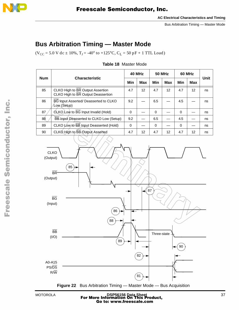
Bus Arbitration Timing — Master Mode(VCC = 5.0 V dc ± 10%, TJ = -40° to +125°C, CL = 50 pF + 1 TTL Load)
Figure 22 Bus Arbitration Timing — Master Mode — Bus Acquisition
Table 18 Master Mode
Num Characteristic40 MHz 50 MHz 60 MHz
UnitMin Max Min Max Min Max
85 CLKO High to BR Output Assertion CLKO High to BR Output Deassertion
4.7 12 4.7 12 4.7 12 ns
86 BG Input Asserted/ Deasserted to CLKO Low (Setup)
9.2 — 6.5 — 4.5 — ns
87 CLKO Low to BG Input Invalid (Hold) 0 — 0 — 0 — ns
88 BB Input Deasserted to CLKO Low (Setup) 9.2 — 6.5 — 4.5 — ns
89 CLKO Low to BB Input Deasserted (Hold) 0 — 0 — 0 — ns
90 CLKO High to BB Output Asserted 4.7 12 4.7 12 4.7 12 ns
86
85
89
88
87
90
81
82
Three-state
CLKO
(Output)
BR(Output)
BG
(Input)
BB(I/O)
A0-A15PS/DS
R/W
Bus Arbitration Timing — Master Mode
Fre
esc
ale
Se
mic
on
du
cto
r, I
Freescale Semiconductor, Inc.
For More Information On This Product, Go to: www.freescale.com
nc
...

AC Electrical Characteristics and Timing
38 DSP56156 Data Sheet MOTOROLA
Figure 23 Bus Arbitration Timing — Master Mode — Bus Release
85
86
87
74
76
75
CLKO(Output)
BR
(Output)
BG(Input)
BB
(I/O)
A0-A15PS/DS
R/W
Bus Arbitration Timing — Master Mode
Fre
esc
ale
Se
mic
on
du
cto
r, I
Freescale Semiconductor, Inc.
For More Information On This Product, Go to: www.freescale.com
nc
...
AC Electrical Characteristics and Timing
MOTOROLA DSP56156 Data Sheet 39
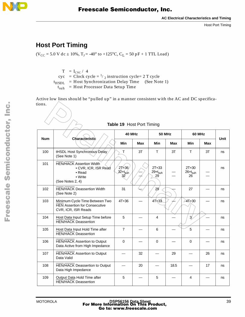
Host Port Timing(VCC = 5.0 V dc ± 10%, TJ = -40° to +125°C, CL = 50 pF + 1 TTL Load)
T = ICYC / 4cyc = Clock cycle = 1/2 instruction cycle= 2 T cycle
tHSDL = Host Synchronization Delay Time (See Note 1)tsuh = Host Processor Data Setup Time
Active low lines should be “pulled up” in a manner consistent with the AC and DC specifica-tions.
Table 19 Host Port Timing
Num Characteristic40 MHz 50 MHz 60 MHz
UnitMin Max Min Max Min Max
100 tHSDL Host Synchronous Delay (See Note 1)
T 3T T 3T T 3T ns
101 HEN/HACK Assertion Width • CVR, ICR, ISR Read
• Read • Write
(See Notes 2, 4)
2T+3632+tsuh
32——
2T+3329+tsuh
29——
2T+3026+tsuh
26——
ns
102 HEN/HACK Deassertion Width (See Note 2)
31 — 29 — 27 — ns
103 Minimum Cycle Time Between Two HEN Assertion for Consecutive CVR, ICR, ISR Reads
4T+36 — 4T+33 — 4T+30 — ns
104 Host Data Input Setup Time before HEN/HACK Deassertion
5 — 4 — 3 — ns
105 Host Data Input Hold Time after HEN/HACK Deassertion
7 — 6 — 5 — ns
106 HEN/HACK Assertion to Output Data Active from High Impedance
0 — 0 — 0 — ns
107 HEN/HACK Assertion to Output Data Valid
— 32 — 29 — 26 ns
108 HEN/HACK Deassertion to Output Data High Impedance
— 20 — 18.5 — 17 ns
109 Output Data Hold Time after HEN/HACK Deassertion
5 — 5 — 4 — ns
Host Port Timing
Fre
esc
ale
Se
mic
on
du
cto
r, I
Freescale Semiconductor, Inc.
For More Information On This Product, Go to: www.freescale.com
nc
...

AC Electrical Characteristics and Timing
40 DSP56156 Data Sheet MOTOROLA
NOTES: 1. “Host Synchronization Delay (tHSDL)” is the time period required for the DSP56156 to sample any external asynchronous input signal, determine whether it is high or low, and synchronize it to the internal clock.
2. See Host Port Considerations.3. HREQ is pulled up by 1 kΩ.4. Only if two consecutive reads from one of these registers are executed.
Table 19 Host Port Timing (continued)
Num Characteristic40 MHz 50 MHz 60 MHz
UnitMin Max Min Max Min Max
110 HR/W Low Setup Time before HEN Assertion 6 — 5 — 4 — ns
111 HR/W Low Hold Time after HEN Deassertion 6 — 5 — 4 — ns
112 HR/W High Setup Time to HEN Assertion 6 — 5 — 4 — ns
113 HR/W High Hold Time after HEN/HACK Deassertion
5 — 4 — 3 — ns
114 HA0-HA2 Setup Time before HEN Assertion 9 — 7.5 — 6 — ns
115 HA0-HA2 Hold Time after HEN Deassertion 8 — 7 — 6 — ns
116 DMA HACK Assertion to HREQ Deassertion (See Note 3)
5 2T+37
5 2T+36
4 2T+35
ns
117 DMA HACK Deassertion to HREQ Assertion (See Note 3)
for DMA RXL Read
for DMA TXL Write
for All Other Cases
tHSDL+3T+5
tHSDL+2T+5
5
—
——
tHSDL3T+5
tHSDL+2T+5
5
—
——
tHSDL+3T+4
tHSDL+2T+4
4
—
——
ns
ns
ns
118 Delay from HEN Deassertion to HREQ Assertion for RXL Read (See Note 3)
tHSDL+3T+5
— tHSDL+3T+5
— tHSDL+3T+4
— ns
119 Delay from HEN Deassertion to HREQ Assertion for TXL Write (See Note 3)
tHSDL+2T+5
— tHSDL+2T+5
— tHSDL+2T+4
— ns
120 Delay from HEN Assertion to HREQ Deassertion for RXL Read, TXL Write(See Note 3)
5 2T+37
5 2T+36
5 2T+35
ns
Host Port Timing
Fre
esc
ale
Se
mic
on
du
cto
r, I
Freescale Semiconductor, Inc.
For More Information On This Product, Go to: www.freescale.com
nc
...

AC Electrical Characteristics and Timing
MOTOROLA DSP56156 Data Sheet 41
Figure 24 Host Synchronization Delay
Figure 25 Host Interrupt Vector Register (IVR) Read
External
Internal
100100
HREQ(Output)
HACK
(Input)
HR/W(Input)
H0-H7
(Output)
102
103
112 113
108107
106 109
Data Valid
101
Host Port Timing
Fre
esc
ale
Se
mic
on
du
cto
r, I
Freescale Semiconductor, Inc.
For More Information On This Product, Go to: www.freescale.com
nc
...

AC Electrical Characteristics and Timing
42 DSP56156 Data Sheet MOTOROLA
Figure 26 Host Read Cycle (Non-DMA Mode)
Figure 27 Host Write Cycle (Non-DMA Mode)
HREQ(Output)
HEN(Input)
HA0-HA2(Input)
HR/W(Input)
H0-H7(Output)
118
120
103
101 102
114 115
112 113
107 108
109
RXL Read
RXH Read
Address Valid
Address Valid
DataValid
DataValid
106
119120
101 102
114 115
TXL Write
TXH Write
Address Valid
Address Valid
DataValid
DataValid
HREQ(Output)
HEN(Input)
HA0-HA2(Input)
HR/W
(Input)
H0-H7(Input)
110 111
104 105
103
Host Port Timing
Fre
esc
ale
Se
mic
on
du
cto
r, I
Freescale Semiconductor, Inc.
For More Information On This Product, Go to: www.freescale.com
nc
...

AC Electrical Characteristics and Timing
MOTOROLA DSP56156 Data Sheet 43
Figure 28 Host Read Cycle (DMA Mode)
Figure 29 Host Write Cycle (DMA Mode)
DataValid
DataValid
RXL Read
RXH Read
HREQ(Output)
HACK(Input)
H0-H7
(Output)
101 102
116 117
107
106
108
109
HREQ(Output)
HACK
(Input)
H0-H7
(Input)
101 102
116 117
104
105
DataValid
DataValid
TXL Write
TXH Write
Host Port Timing
Fre
esc
ale
Se
mic
on
du
cto
r, I
Freescale Semiconductor, Inc.
For More Information On This Product, Go to: www.freescale.com
nc
...

AC Electrical Characteristics and Timing
44 DSP56156 Data Sheet MOTOROLA
Synchronous Serial Interfaces (SSI) Timing(VCC = 5.0 V dc ± 10%, TJ = -40° to + 125°C, CL = 50 pF + 1 TTL Load)
T = ICYC / 4SCK = Serial Clock Pin
FST (Transmit Frame Sync) = SCx0 PinFSR (Receive Frame Sync) = SCx1 Pin
i ck = Internal Clockx ck = External Clock
i ck a = Internal Clock, Asynchronous Mode (Asynchronous implies that FSR and FST are two different frame syncs)
i ck s = Internal Clock, Synchronous Mode (Synchronous implies that only one frame sync FS is used)
bl = bit lengthwl = word length
NOTE: All the timings for the SSI are given for a non-inverted serial clock polarity (SCKP=0 in CRB) and a non-inverted frame sync (FSI=0 in CRB). If the polarity of the clock and/or the frame sync have been inverted, all the timings remain valid by inverting the clock signal SCK and/or the frame sync FSR/FST in the tables and in the figures.
Table 20 Synchronous Serial Interfaces Timing
Num Characteristic40/50/60 MHz
Case UnitMin Max
130 Clock Cycle (See Note) 100 — — ns
131 Clock High Period 45 — — ns
132 Clock Low Period 45 — — ns
133 Output Clock Rise/Fall Time — 7 — ns
134 SCK Rising Edge to FSR Out (bl) High
——
3218
x cki ck a
ns
135 SCK Rising Edge to FSR Out (bl) Low
——
3215
x cki ck a
ns
136 SCK Rising Edge to FSR Out (wl) High
——
3215
x cki ck a
ns
137 SCK Rising Edge to FSR Out (wl) Low
——
3215
x cki ck a
ns
138 Data In Setup Time before SCK Falling Edge
3040
——
x cki ck
ns
139 Data In Hold Time after SCK Falling Edge
2512
——
x cki ck
ns
SSI Timing
Fre
esc
ale
Se
mic
on
du
cto
r, I
Freescale Semiconductor, Inc.
For More Information On This Product, Go to: www.freescale.com
nc
...

AC Electrical Characteristics and Timing
MOTOROLA DSP56156 Data Sheet 45
SSI Timing
Fre
esc
ale
Se
mic
on
du
cto
r, I
Freescale Semiconductor, Inc.
For More Information On This Product, Go to: www.freescale.com
nc
...

AC Electrical Characteristics and Timing
46 DSP56156 Data Sheet MOTOROLA
Table 20 Synchronous Serial Interfaces Timing (continued)
Num Characteristic40/50/60MHz
Case UnitMin Max
140 FSR Input (bl) High before SCK Falling Edge
715
——
x cki ck a
ns
141 FSR Input (wl) High before SCK Falling Edge
715
——
x cki ck a
ns
142 FSR Input Hold Time after SCK Falling Edge
157
——
x cki ck a
ns
143 Flags Input Setup before SCK Falling Edge
715
——
x cki ck
ns
144 Flags Input Hold Time after SCK Falling Edge
157
——
x cki ck
ns
145 SCK Rising Edge to FST Out (bl) High
——
3315
x cki ck
ns
146 SCK Rising Edge to FST Out(bl) Low
——
3015
x cki ck
ns
147 SCK Rising Edge to FST Out (wl) High
——
3015
x cki ck
ns
148 SCK Rising Edge to FST Out(wl) Low
——
3315
x cki ck
ns
149 SCK Rising Edge to Data Out Enable from High Impedance
——
3012
x cki ck
ns
150 SCK Rising Edge to Data Out Valid ——
3012
x cki ck
ns
151 SCK Rising Edge to Data Out High Impedance
——
3020
x cki ck
ns
152 FST Input (bl) Setup Time before SCK Falling Edge
616
——
x cki ck
ns
153 FST Input (wl) to Data Out Enable from High Impedance
— 36 — ns
154 FST Input (wl) Setup Time before SCK Falling Edge
817
——
x cki ck
ns
155 FST Input Hold Time after SCK Falling Edge
154
——
x cki ck
ns
156 Flag Output Valid after SCK Rising Edge
——
3215
x cki ck
ns
SSI Timing
Fre
esc
ale
Se
mic
on
du
cto
r, I
Freescale Semiconductor, Inc.
For More Information On This Product, Go to: www.freescale.com
nc
...
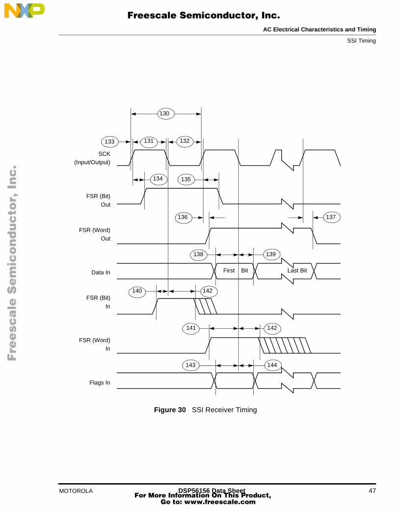
AC Electrical Characteristics and Timing
MOTOROLA DSP56156 Data Sheet 47
Figure 30 SSI Receiver Timing
SCK(Input/Output)
FSR (Bit)
Out
FSR (Word)Out
Data In
FSR (Bit)
In
FSR (Word)In
Flags In
First Bit Last Bit
131 132133
130
134 135
136 137
138 139
140 142
142141
143 144
SSI Timing
Fre
esc
ale
Se
mic
on
du
cto
r, I
Freescale Semiconductor, Inc.
For More Information On This Product, Go to: www.freescale.com
nc
...

AC Electrical Characteristics and Timing
48 DSP56156 Data Sheet MOTOROLA
Figure 31 SSI Transmitter Timing
NOTE: In the Network mode, output flag transitions can occur at the start of each time slot within the frame. In the Normal mode, the output flag state is asserted for the entire frame period.
150
151
155
152
153
155
156
First Bit Last Bit
(See Note)
132
130
133 131
145 146
147 148
149
150
SCK(Input/Output)
FST (Bit)
Out
FST (Word)Out
Data Out
FST (Bit)In
FST (Word)In
Flags Out
154
Timer Timing
Fre
esc
ale
Se
mic
on
du
cto
r, I
Freescale Semiconductor, Inc.
For More Information On This Product, Go to: www.freescale.com
nc
...
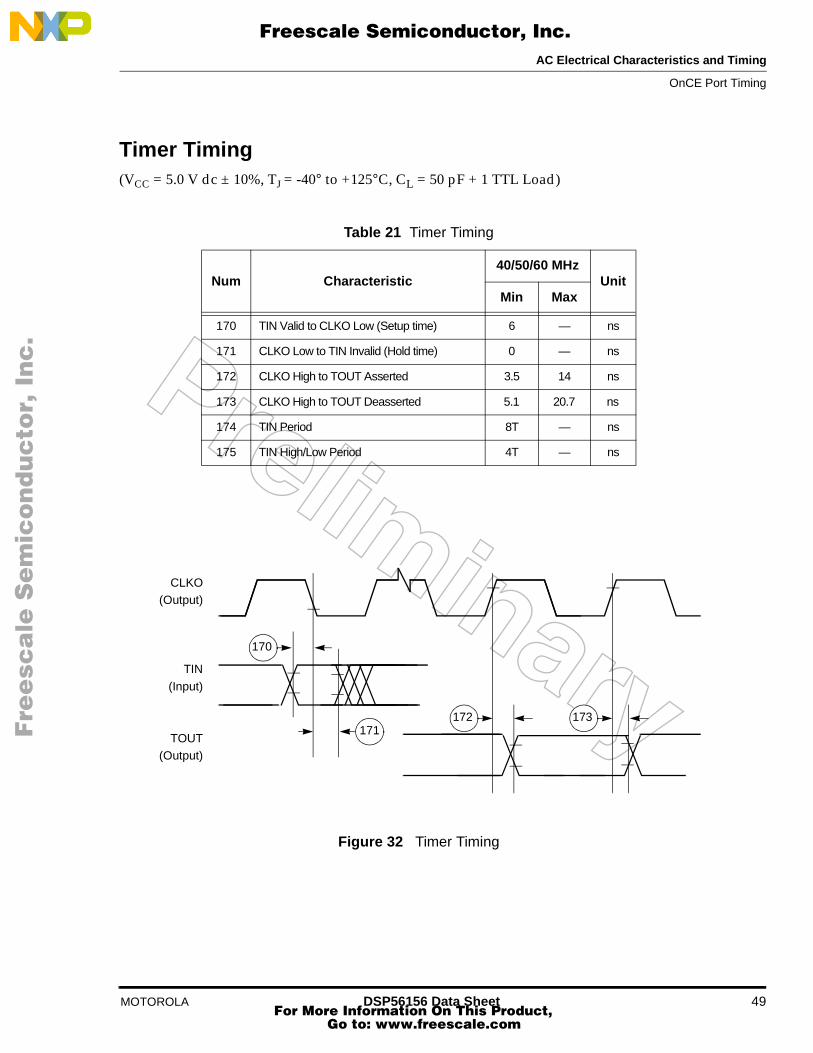
AC Electrical Characteristics and Timing
MOTOROLA DSP56156 Data Sheet 49
Timer Timing(VCC = 5.0 V dc ± 10%, TJ = -40° to +125°C, CL = 50 pF + 1 TTL Load)
Figure 32 Timer Timing
Table 21 Timer Timing
Num Characteristic40/50/60 MHz
UnitMin Max
170 TIN Valid to CLKO Low (Setup time) 6 — ns
171 CLKO Low to TIN Invalid (Hold time) 0 — ns
172 CLKO High to TOUT Asserted 3.5 14 ns
173 CLKO High to TOUT Deasserted 5.1 20.7 ns
174 TIN Period 8T — ns
175 TIN High/Low Period 4T — ns
170
172171
173
CLKO(Output)
TIN
(Input)
TOUT(Output)
OnCE Port Timing
Fre
esc
ale
Se
mic
on
du
cto
r, I
Freescale Semiconductor, Inc.
For More Information On This Product, Go to: www.freescale.com
nc
...
AC Electrical Characteristics and Timing
50 DSP56156 Data Sheet MOTOROLA
OnCETM Port Timing
(VCC = 5.0 V dc ± 10%, TJ = -40° to +125°C, CL = 50 pF + 1 TTL Load)
NOTES: 1. 45%-55% duty cycle2. Td = DSCK High (Timing #183)
Table 22 OnCE Port Timing
Num Characteristic40/50/60 MHz
UnitMin Max
180 DSCK High to DSO Valid — 37 ns
181 DSI Valid to DSCK Low (Setup) 5.2 — ns
182 DSCK Low to DSI Invalid (Hold) 0 — ns
183 DSCK High (See Note 1) 2Tc — ns
184 DSCK Low (See Note 1) 2Tc — ns
185 DSCK Cycle Time (See Note 1) 4Tc — ns
186 CLKO High to OS0-OS1 Valid 14.5 ns
187 CLKO High to OS0-OS1 Invalid — — ns
188 Last DSCK High to OS0-OS1 (See Note 2)Last DSCK High to ACK Active (data) (See Note 2)Last DSCK High to ACK Active (command) (See Note 2)
10T+Td+14.510T+Td+13.521T+Td+13.5
——
ns
189 DSO (ACK) Asserted to OS0-OS1 Three-state — 0 ns
190 DSO (ACK) Asserted to First DSCK High 3Tc — ns
191 DSO (ACK) Width Asserted:• when entering debug mode
• when acknowledging command/data transfer3T-2
2Tc+0.53T-5
2Tc+3nsns
192 Last DSCK High of Read Register to FirstDSCK High of Next Command
6Tc — ns
193 DSCK High to DSO Invalid (See Note 2) Td+11.2 — ns
194 DR asserted to DSO (ACK) Asserted 11T+19.5 — ns
OnCE Port Timing
Fre
esc
ale
Se
mic
on
du
cto
r, I
Freescale Semiconductor, Inc.
For More Information On This Product, Go to: www.freescale.com
nc
...
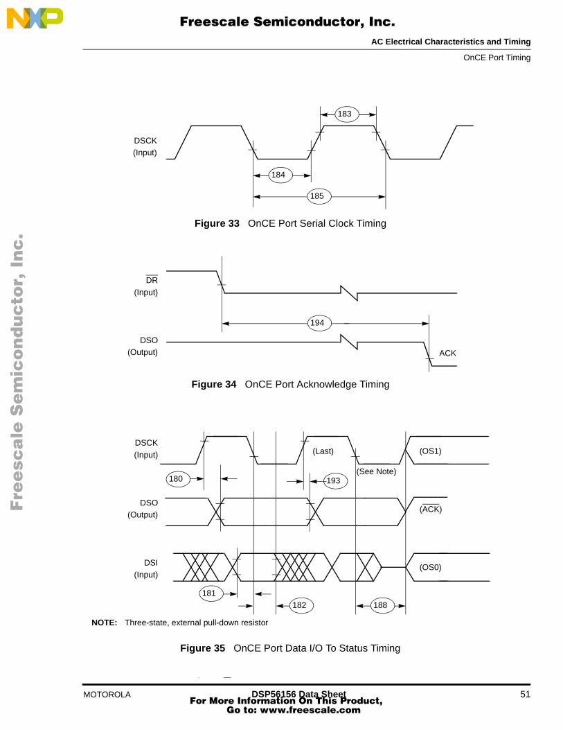
AC Electrical Characteristics and Timing
MOTOROLA DSP56156 Data Sheet 51
Figure 33 OnCE Port Serial Clock Timing
Figure 34 OnCE Port Acknowledge Timing
Figure 35 OnCE Port Data I/O To Status Timing
DSCK(Input)
185
183
184
194
ACK
DR
(Input)
DSO(Output)
188
(ACK)
(OS0)
(OS1)(Last)DSCK
(Input)
DSO(Output)
DSI(Input)
193180
181182
(See Note)
NOTE: Three-state, external pull-down resistor
OnCE Port Timing
Fre
esc
ale
Se
mic
on
du
cto
r, I
Freescale Semiconductor, Inc.
For More Information On This Product, Go to: www.freescale.com
nc
...

Pin-out and Package
52 DSP56156 Data Sheet MOTOROLA
Pin-out and Package Information
Figure 39 Top View of the DSP56156 112-pin Plastic (FC) and Ceramic (FE) Quad Flat Packages
GND4D2D3
VCC3D4D5
GND5D6D7D8D9
GND6D10D11
VCC4
D12D13
GND7D14D15
TADR
VCCASPKPSPKMGNDAVDIV
VREF
Orientation Mark
1
29
57
85
D1
D0
A15
A14
GN
D3
A13
A12
A11
GN
DQ
1V
CC
2A
10G
ND
2A
9A
8A
7A
6V
CC
Q1
GN
D1
A5
A4
VC
C1
A3
A2
GN
D0
A1
A0
MO
DC
MO
DB
/IRQ
B
NOTE: An OVERBAR indicates the signal is asserted when the voltage = ground (active low).
MIC
AU
XB
IAS
BG
VC
CQ
0B
RB
BV
CC
5W
RG
ND
8R
DP
S/D
SB
SR
/WD
SO
DS
CK
/OS
1D
SI/O
S0
CLK
OG
ND
Q0
GN
DS
SX
FC
VC
CS
EX
TAL
SC
01/P
C9
GN
D9
SC
11/P
C8
SC
K1/
PC
7H
7/P
B7
(Top View)
MODA/IRQARESETSTD0/PC0SRD0/PC1SCK0/PC2SC10/PC3SC00/PC4TIN/PC10VCC7
TOUT/PC11HA0/PB8GND10HA1/PB9HA2/PB10HR/W/PB11HEN/PB12HACK/PB14HREQ/PB13H0/PB0H1/PB1STD1/PC5SRD1/PC6H4/PB4H3/PB3H2/PB2VCC6H5/PB5H6/PB6
Top View
Fre
esc
ale
Se
mic
on
du
cto
r, I
Freescale Semiconductor, Inc.
For More Information On This Product, Go to: www.freescale.com
nc
...
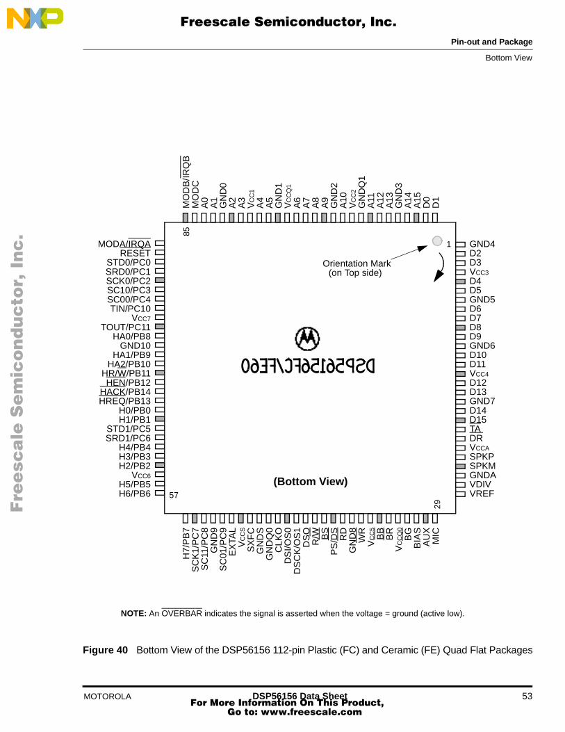
Pin-out and Package
MOTOROLA DSP56156 Data Sheet 53
Figure 40 Bottom View of the DSP56156 112-pin Plastic (FC) and Ceramic (FE) Quad Flat Packages
NOTE: An OVERBAR indicates the signal is asserted when the voltage = ground (active low).
MODA/IRQARESET
STD0/PC0SRD0/PC1SCK0/PC2SC10/PC3SC00/PC4TIN/PC10
VCC7
TOUT/PC11HA0/PB8
GND10HA1/PB9
HA2/PB10HR/W/PB11HEN/PB12
HACK/PB14HREQ/PB13
H0/PB0H1/PB1
STD1/PC5SRD1/PC6
H4/PB4H3/PB3H2/PB2
VCC6H5/PB5H6/PB6
GND4D2D3VCC3D4D5GND5D6D7D8D9GND6D10D11VCC4
D12D13GND7D14D15TADRVCCASPKPSPKMGNDAVDIVVREF
Orientation Mark
1
29
57
85
H7/
PB
7S
CK
1/P
C7
SC
11/P
C8
GN
D9
SC
01/P
C9
EX
TAL
VC
CS
SX
FC
GN
DS
GN
DQ
0C
LKO
DS
I/OS
0D
SC
K/O
S1
DS
OR
/W BS
PS
/DS
RD
GN
D8
WR
VC
C5
BB
BR
VC
CQ
0
BG
BIA
SA
UX
MIC
MO
DB
/IRQ
BM
OD
CA
0A
1G
ND
0A
2A
3V
CC
1A
4A
5G
ND
1V
CC
Q1
A6
A7
A8
A9
GN
D2
A10
VC
C2
GN
DQ
1A
11A
12A
13G
ND
3A
14A
15D
0D
1
(on Top side)
(Bottom View)
Bottom View
Fre
esc
ale
Se
mic
on
du
cto
r, I
Freescale Semiconductor, Inc.
For More Information On This Product, Go to: www.freescale.com
nc
...

Pin-out and Package
54 DSP56156 Data Sheet MOTOROLA
Table 23 DSP56156 General Purpose I/O Pin Identification
112-pin Package
Pin #
DSP56156 Primary Pin
Function
DSP56156 General
Purpose I/O ID
66 H0 PB0
65 H1 PB1
60 H2 PB2
61 H3 PB3
62 H4 PB4
58 H5 PB5
57 H6 PB6
56 H7 PB7
74 HA0 PB8
72 HA1 PB9
71 HA2 PB10
70 HR/W PB11
69 HEN PB12
67 HREQ PB13
68 HACK PB14
82 STD0 PC0
81 SRD0 PC1
80 SCK0 PC2
79 SC10 PC3
78 SC00 PC4
64 STD1 PC5
63 SRD1 PC6
55 SCK1 PC7
54 SC11 PC8
52 SC01 PC9
77 TIN PC10
75 TOUT PC11
General Purpose I/O
NOTES: 1. In Tables 23, 24, and 25, OVERBAR indicates the signal is asserted when the voltage = ground (active low).
2. For more information on power and ground, see Table 26 under Design Considerations.
Fre
esc
ale
Se
mic
on
du
cto
r, I
Freescale Semiconductor, Inc.
For More Information On This Product, Go to: www.freescale.com
nc
...

Pin-out and Package
MOTOROLA DSP56156 Data Sheet 55
Pin Number
Fre
esc
ale
Se
mic
on
du
cto
r, I
Freescale Semiconductor, Inc.
For More Information On This Product, Go to: www.freescale.com
nc
...

Pin-out and Package
56 DSP56156 Data Sheet MOTOROLA
Table 24 DSP56156 Pin Identification by Pin Number
112-pin Package
Pin #Signal Name
112-pin Package
Pin #Signal Name
112-pin Package
Pin #Signal Name
1 GND4 39 RD 76 VCC7
2 D2 40 PS/DS 77 TIN/PC10
3 D3 41 BS 78 SC00/PC4
4 VCC3 42 R/W 79 SC10/PC3
5 D4 43 DSO 80 SCK0/PC2
6 D5 44 DSCK/OS1 81 SRD0/PC1
7 GND5 45 DSI/OS0 82 STD0/PC0
8 D6 46 CLKO 83 RESET
9 D7 47 GNDQ0 84 MODA/IRQA
10 D8 48 GNDS 85 MODB/IRQB
11 D9 49 SXFC 86 MODC
12 GND6 50 VCCS 87 A0
13 D10 51 EXTAL 88 A1
14 D11 52 SC01/PC9 89 GND0
15 VCC4 53 GND9 90 A2
16 D12 54 SC11/PC8 91 A3
17 D13 55 SCK1/PC7 92 VCC1
18 GND7 56 H7/PB7 93 A4
19 D14 57 H6/PB6 94 A5
20 D15 58 H5/PB5 95 GND1
21 TA 59 VCC6 96 VCCQ1
22 DR 60 H2/PB2 97 A6
23 VCCA 61 H3/PB3 98 A7
24 SPKP 62 H4/PB4 99 A8
25 SPKM 63 SRD1/PC6 100 A9
26 GNDA 64 STD1/PC5 101 GND2
27 VDIV 65 H1/PB1 102 A10
28 VREF 66 H0/PB0 103 VCC2
29 MIC 67 HREQ/PB13 104 GNDQ1
30 AUX 68 HACK/PB14 105 A11
31 BIAS 69 HEN/PB12 106 A12
32 BG 70 HR/W/PB11 107 A13
33 VCCQ0 71 HA2/PB10 108 GND3
34 BR 72 HA1/PB9 109 A14
35 BB 73 GND10 110 A15
36 VCC5 74 HA0/PB8 111 D0
37 WR 75 TOUT/PC11 112 D1
38 GND8
Signal Name
Fre
esc
ale
Se
mic
on
du
cto
r, I
Freescale Semiconductor, Inc.
For More Information On This Product, Go to: www.freescale.com
nc
...

Pin-out and Package
MOTOROLA DSP56156 Data Sheet 57
Signal Name
Fre
esc
ale
Se
mic
on
du
cto
r, I
Freescale Semiconductor, Inc.
For More Information On This Product, Go to: www.freescale.com
nc
...

Pin-out and Package
58 DSP56156 Data Sheet MOTOROLA
Table 25 DSP56156 Pin Identification by Signal Name
112-pin Package
Pin #Signal Name
112-pin Package
Pin #Signal Name
112-pin Package
Pin #Signal Name
87 A0 6 D5 47 GNDQ0
88 A1 8 D6 104 GNDQ1
90 A2 9 D7 48 GNDS
91 A3 10 D8 66 H0
93 A4 11 D9 65 H1
94 A5 13 D10 60 H2
97 A6 14 D11 61 H3
98 A7 16 D12 62 H4
99 A8 17 D13 58 H5
100 A9 19 D14 57 H6
102 A10 20 D15 56 H7
105 A11 22 DR 74 HA0
106 A12 44 DSCK 72 HA1
107 A13 45 DSI 71 HA2
109 A14 43 DSO 68 HACK
110 A15 51 EXTAL 69 HEN
30 AUX 89 GND0 70 HR/W
35 BB 95 GND1 67 HREQ
32 BG 101 GND2 84 IRQA
31 BIAS 108 GND3 85 IRQB
34 BR 1 GND4 29 MIC
41 BS 7 GND5 84 MODA
46 CLKO 12 GND6 85 MODB
111 D0 18 GND7 86 MODC
112 D1 38 GND8 45 OS0
2 D2 53 GND9 44 OS1
3 D3 73 GND10 66 PB0
5 D4 26 GNDA 65 PB1
Fre
esc
ale
Se
mic
on
du
cto
r, I
Freescale Semiconductor, Inc.
For More Information On This Product, Go to: www.freescale.com
nc
...

Pin-out and Package
MOTOROLA DSP56156 Data Sheet 59
Fre
esc
ale
Se
mic
on
du
cto
r, I
Freescale Semiconductor, Inc.
For More Information On This Product, Go to: www.freescale.com
nc
...

Pin-out and Package
60 DSP56156 Data Sheet MOTOROLA
Table 25 DSP56156 Pin Identification by Signal Name (continued)
112-pin Package
Pin #Signal Name
112-pin Package
Pin #Signal Name
112-pin Package
Pin #Signal Name
60 PB2 55 PC7 64 STD1
61 PB3 54 PC8 49 SXFC
62 PB4 52 PC9 21 TA
58 PB5 77 PC10 77 TIN
57 PB6 75 PC11 75 TOUT
56 PB7 40 PS/DS 92 VCC1
74 PB8 42 R/W 103 VCC2
72 PB9 39 RD 4 VCC3
71 PB10 83 RESET 15 VCC4
70 PB11 78 SC00 36 VCC5
69 PB12 52 SC01 59 VCC6
67 PB13 79 SC10 76 VCC7
68 PB14 54 SC11 23 VCCA
82 PC0 80 SCK0 33 VCCQ0
81 PC1 55 SCK1 96 VCCQ1
80 PC2 25 SPKM 50 VCCS
79 PC3 24 SPKP 27 VDIV
78 PC4 81 SRD0 28 VREF
64 PC5 63 SRD1 37 WR
63 PC6 82 STD0
Fre
esc
ale
Se
mic
on
du
cto
r, I
Freescale Semiconductor, Inc.
For More Information On This Product, Go to: www.freescale.com
nc
...

Pin-out and Package
MOTOROLA DSP56156 Data Sheet 61
112 CQFP
Fre
esc
ale
Se
mic
on
du
cto
r, I
Freescale Semiconductor, Inc.
For More Information On This Product, Go to: www.freescale.com
nc
...
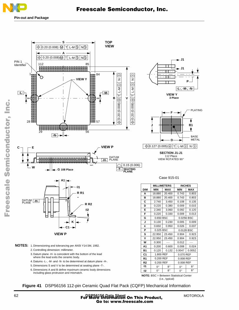
Pin-out and Package
62 DSP56156 Data Sheet MOTOROLA
-L-
VIEW Y
PIN 1Identifier 112
1
28
29 56
57
84
85
C E
WG 108 Place
VIEW P
0.15 (0.006)
0.20 (0.008) T L-M S N SM
0.20 (0.008) T L-M S N SM
0.20
(0.
008)
TL-
MN
0.20
(0.
008)
TL-
MN
A
S
-M-
B V
-N-
-H- DATUMPLANE
-T- SEATINGPLANE
J1
J1
P
VIEW Y3 Place
-L-, -M-, -N-
A1
θ1
θ2
R R1
R R2
K
-H-DATUMPLANE
VIEW P
C1
MIN MINMAX MAXMILLIMETERS INCHES
DIMA
BC
DE
FG
JK
P
SV
WA1
B1C1
R1R2
θ2
18.880
18.880
2.740
0.220
2.340
0.220
0.130
0.650
22.950
22.950
0.300
0.200
0.120
0°
20.400
20.400
3.450
0.380
3.060
0.330
0.230
0.950
23.450
23.450
0.600
0.132
0.743
0.743
0.108
0.009
0.092
0.009
0.005
0.026
0.904
0.904
0.012
0.008
0.0047
0.803
0.803
0.135
0.015
0.120
0.013
0.009
0.037
0.923
0.923
0.024
0.0052
0.650 BSC 0.0256 BSC
0.325 BSC 0.0128 BSC
1.800 REF 0.070 REF0.200 REF 0.008 REF
0.200 REF 0.008 REF
NOTES: 1. Dimensioning and tolerancing per ANSI Y14.5M, 1982.
2. Controlling dimension: millimeter.
3. Datum plane -H- is coincident with the bottom of the lead where the lead exits the ceramic body.
4. Datums -L-, -M- and -N- to be determined at datum plane -H-.
5. Dimensions S and V to be determined at seating plane -T-.
6. Dimensions A and B define maximum ceramic body dimensions including glass protrusion and mismatch.
θ1
0°8°8°
0°0°
8°8°
M0.127 (0.005) T L-M N
BASEMETAL
PLATING
SECTION J1-J1112 Place
VIEW ROTATED 90°
F
D
J B1
Figure 41 DSP56156 112-pin Ceramic Quad Flat Pack (CQFP) Mechanical Information
S S
MM
SS
SS
NOTE: BSC = Between Statistical Center (i.e., typical)
TOPVIEW
Case 915-01
Fre
esc
ale
Se
mic
on
du
cto
r, I
Freescale Semiconductor, Inc.
For More Information On This Product, Go to: www.freescale.com
nc
...
Pin-out and Package
MOTOROLA DSP56156 Data Sheet 63
112 TQFP
Fre
esc
ale
Se
mic
on
du
cto
r, I
Freescale Semiconductor, Inc.
For More Information On This Product, Go to: www.freescale.com
nc
...

Pin-out and Package
64 DSP56156 Data Sheet MOTOROLA
0.100 (0.004)C
C2 VIEW AB
SEATINGPLANE-T-
-L-, -M-, -N-
VIEW Y
J1
J1
F
J
D
BASEMETAL
AA
SECTION J1-J1(VIEW ROTATED 90° COUNTER CLOCKWISE)
VIEW AB
θ1
R2
R1
0.13 (0.005) T L -M M C MM
VIEW Y
DIM MIN MAX MIN MAX
INCHESMILLIMETERS
A 20.000 BSC 0.790 BSC
A1 10.000 BSC 0.395 BSC
B 20.000 BSC 0.790 BSC
B1 10.000 BSC 0.395 BSC
C 1.400 1.600 0.055 0.063
C1 0.050 0.150 0.002 0.006
C2 1.350 1.450 0.053 0.057
D 0.270 0.370 0.011 0.014
E 0.450 0.750 0.018 0.030
F 0.270 0.330 0.011 0.013
G 0.650 BSC 0.0256 BSC
J 0.115 0.175 0.006 0.007
K 0.500 BSC 0.020 BSC
P 0.325 BSC 0.013 BSC
R1 0.100 0.200 0.004 0.008
R2 0.100 0.200 0.004 0.008
S 22.000 BSC 0.866 BSC
S1 11.000 BSC 0.433 BSC
V 22.000 BSC 0.866 BSC
V1 11.000 BSC 0.433 BSC
Y 0.250 REF 0.010 REF
Z 1.000 REF 0.039 REF
AA 0.115 0.135 0.004 0.005
θθ1
θ2
θ3
PIN 1 Identifier 112 85
84
56
28 57
1
29
-L- -M-
-N-
V1
S1
0°3°
11°11°
0°3°
11°11°
8°7°
13°13°
8°7°
13°13°
0.200 (0.008) T L-M N0.200 (0.008) H L-M N4x
4x 28 TIPS
θ3
θ2
S
A
VB
B1
A1
θ
C1
0.25 (0.010)
4x P
108x G
GAGE PLANE
0.050 (0.002) S
-H-
Y
K
E
Z
NOTES: 1. Dimensioning and tolerancing per ANSI Y14.5M, 1982. 2. Controlling dimension: Millimeter. 3. Datum plane -H- is located at bottom of lead and is coincident with the lead
where the lead exits the plastic body at the bottom of the parting line. 4. Datums -L-, -M- and -N- to be determined at datum plane -H-. 5. Dimensions S and V to be determined at seating plane -T-. 6. Dimensions A and B do not include mold protrusion. Allowable protrusion is
0.25 (0.010) per side. Dimensions A and B do include mold mismatch and are determined at datum plane -H-.
7. Dimension D does not include dambar protrusion. Allowable dambar protrusion shall not cause the D dimension to exceed 0.43 (0.017).
Figure 42 DSP56156 112-pin Plastic Thin Quad Flat Pack (TQFP) Mechanical Information
NOTE: BSC = Between Statistical Center (i.e., typical)
TOPVIEW
Case 987-01
Fre
esc
ale
Se
mic
on
du
cto
r, I
Freescale Semiconductor, Inc.
For More Information On This Product, Go to: www.freescale.com
nc
...
Design Considerations
60 DSP56156 Data Sheet MOTOROLA
Design Considerations ΘJC is device-related and cannot be influ-enced by the user. However, ΘCA is user-de-pendent and can be minimized by such thermal management techniques as heat sinks, ambient air cooling, and thermal con-vection. Thus, good thermal management on the part of the user can significantly reduce ΘCA so that ΘJA approximately equals ΘJC. Substitution of ΘJC for ΘJA in equation (1) will result in a lower semiconductor junction temperature. Values for thermal resistance presented in this document, unless estimat-ed, were derived using the procedure de-scribed in Motorola Reliability Report 7843, “Thermal Resistance Measurement Method for MC68XX Microcomponent Devices”, and are provided for design purposes only. Ther-mal measurements are complex and depen-dent on procedure and setup. User-derived values for thermal resistance may differ.
Power, Ground, and NoiseEach DSP56156 VCC pin should be provided with a low-impedance path to +5 volts. Each DSP56156 GND pin should likewise be pro-vided with a low-impedance path to ground. The power supply pins drive distinct groups of logic on chip as shown in Table 26.
The VCC power supply should be by-passed to GND ground using at least six 0.01 – 0.1 µF bypass capacitors located ei-ther underneath the chip’s socket or as close as possible to the four sides of the package. The capacitor leads and the associated printed circuit traces connecting to chip VCC and GND should be kept to less than 0.5” per
Heat DissipationThe average chip junction temperature, TJ, in °C, can be obtained from:
TJ = TA + (PD × ΘJA) (1)
Where:TA = ambient temperature, °CΘJA = package thermal resistance,
junction-to-ambient, °C/WPD = PINT + PI/OPINT = ICC × VCC watts — chip internal
power
PI/O = power dissipation on input and output pins — user determined
For most applications PI/O < PINT and PI/O can be neglected. An appropriate relationship be-tween PD and TJ (if PI/O is neglected) is:
PD = K/(TJ + 273) (2)
Solving equations (1) and (2) for K gives:
K = PD × (TA + 273) + PD × ΘJA (3)
Where K is a constant pertaining to the partic-ular package. K can be determined from equation (2) by measuring PD (at equilibri-um) for a known TA. Using this value of K, the values of PD and TJ can be obtained by solv-ing equations (1) and (2) iteratively for any value of TA. The total thermal resistance of a package (ΘJA) can be separated into two com-ponents, ΘJC and ΘCA, representing the barrier to heat flow from the semiconductor junction to the package (case) surface (ΘJC) and from the case to the outside ambient (ΘCA). These terms are related by the equation:
ΘJA = ΘJC + ΘCA (4)
Heat DissipationPower, Ground, and Noise
Fre
esc
ale
Se
mic
on
du
cto
r, I
Freescale Semiconductor, Inc.
For More Information On This Product, Go to: www.freescale.com
nc
...

Design Considerations
MOTOROLA DSP56156 Data Sheet 61
capacitor lead. The use of at least a four lay-er board is recommended, employing two inner layers as VCC and GND planes. All output pins on this DSP have fast rise and fall times. Printed Circuit Board (PCB) trace length should be minimized in order to minimize undershoot and reflections caused by these fast output switching times. This recommendation particularly applies to the address and data buses as well as the PS/DS, BS, RD, WR, R/W, inter-rupt, and HEN pins. Maximum PCB trace lengths on the order of 6" are recommended. Capacitance calculations should consider all
device loads as well as parasitic capacitanc-es due to PCB traces. Attention to proper PCB layout and bypassing becomes espe-cially critical in systems with higher capac-itive loads because these loads create higher transient currents in the VCC and GND circuits.
Clock signals should not be run across many signals and should be kept away from analog power and ground traces as well as any analog signals. See Figure 44 for more details.
Power, Ground, and Noise
Table 26 Power and Ground Connections
Circuitry
Power Ground
Signal Name
Pin #Signal Name
Pin #
Address Bus Buffers VCC1VCC2
92103
GND0GND1GND2GND3
8995
101108
Data Bus Buffers VCC3VCC4
415
GND4GND5GND6GND7
17
1218
Bus Control Buffers VCC5 36 GND8 38
Codec VCCA 23 GNDA 26
Digital Peripherals VCC6VCC7
5976
GND9GND10
5373
Internal logic VCCQ0VCCQ1
3396
GNDQ0GNDQ1
47104
Phase-Locked Loop (PLL) VCCS 50 GNDS 48
Fre
esc
ale
Se
mic
on
du
cto
r, I
Freescale Semiconductor, Inc.
For More Information On This Product, Go to: www.freescale.com
nc
...
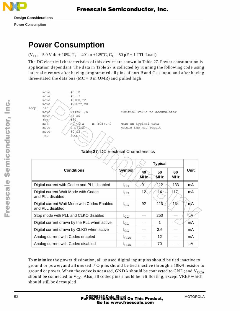
Design Considerations
62 DSP56156 Data Sheet MOTOROLA
Power Consumption(VCC = 5.0 V dc ± 10%, TJ = -40° to +125°C, CL = 50 pF + 1 TTL Load)
The DC electrical characteristics of this device are shown in Table 27. Power consumption is application dependant. The data in Table 27 is collected by running the following code using internal memory after having programmed all pins of port B and C as input and after having three-stated the data bus (MC = 0 in OMR) and pulled high:
move #0,r0move #0,r3move #$100,r2move #$00ff,m0
loop clr amove x:(r0)+,a ;initial value to accumulatormove a1,a0rep #30mac x0,y0,a x:(r3)+,x0 ;mac on typical datamove a,p:(r2) ;store the mac resultmove #0,r3jmp loop
To minimize the power dissipation, all unused digital input pins should be tied inactive to ground or power; and all unused I/O pins should be tied inactive through a 10K¾ resistor to ground or power. When the codec is not used, GNDA should be connected to GND; and VCCA should be connected to VCC. Also, all codec pins should be left floating, except VREF which should still be decoupled.
Table 27 DC Electrical Characteristics
Conditions Symbol
Typical
Unit40 MHz
50 MHz
60 MHz
Digital current with Codec and PLL disabled ICC 91 112 133 mA
Digital current Wait Mode with Codec and PLL disabled
ICC 12 14 17 mA
Digital current Wait Mode with Codec Enabled and PLL disabled
ICC 92 113 134 mA
Stop mode with PLL and CLKO disabled ICC — 250 — µA
Digital current drawn by the PLL when active ICC — 1 — mA
Digital current drawn by CLKO when active ICC — 3.6 — mA
Analog current with Codec enabled ICCA — 12 — mA
Analog current with Codec disabled ICCA — 70 — µA
Power Consumption
Fre
esc
ale
Se
mic
on
du
cto
r, I
Freescale Semiconductor, Inc.
For More Information On This Product, Go to: www.freescale.com
nc
...

Design Considerations
MOTOROLA DSP56156 Data Sheet 63
Host Port ConsiderationsCareful synchronization is required when reading multi-bit registers that are written by another asynchronous system. This is a com-mon problem when two asynchronous sys-tems are connected. The situation exists in the host interface. The considerations for proper operation are discussed below.
Host Programming Considerations1. Unsynchronized Reading of
Receive Byte RegistersWhen reading receive byte registers, RXH or RXL, the host program should use interrupts or poll the RXDF flag which indicates that data is available. This assures that the data in the receive byte registers will be stable.
2. Overwriting Transmit Byte RegistersThe host program should not write to the transmit byte registers, TXH or TXL, un-less the TXDE bit is set indicating that the transmit byte registers are empty. This guarantees that the transmit byte regis-ters will transfer valid data to the HRX register.
3. Synchronization of Status Bits from DSP to Host HC, HREQ, DMA, HF3, HF2, TRDY, TXDE, and RXDF status bits are set or cleared from inside the DSP and read by the host processor (refer to DSP56156 Us-er’s Manual, I/O Interface section, Host/DMA Interface Programming Model for descriptions of these status bits). The host can read these status bits very quick-ly without regard to the clock rate used
by the DSP, but the possibility exists that the state of the bit could be changing dur-ing the read operation. This is generally not a system problem, since the bit will be read correctly in the next pass of any host polling routine.
However, if the host asserts HEN for more than timing number 101 (T101), with a minimum cycle time of timing number 103 (T103), then these status bits are guaranteed to be stable. Care must be exercised when reading status bits HF3 and HF2 as an encoded pair. If the DSP changes HF3 and HF2 from 00 to 11, there is a small probability that the host could read the bits during the transition and receive 01 or 10 instead of 11. If the combination of HF3 and HF2 has signif-icance, the host could read the wrong combination. Therefore, read the bits twice and check for consensus.
4. Overwriting the Host VectorThe host program should change the Host Vector register only when the Host Command bit (HC) is clear. This change will guarantee that the DSP interrupt control logic will receive a stable vector.
5. Cancelling a Pending Host Command ExceptionThe host processor may elect to clear the HC bit to cancel the host command ex-ception request at any time before it is recognized by the DSP. Because the host does not know exactly when the excep-tion will be recognized (due to exception processing synchronization and pipeline delays), the DSP may execute the host command exception after the HC bit is cleared. For these reasons, the HV bits must not be changed at the same time that the HC bit is cleared.
Host Port Considerations
Fre
esc
ale
Se
mic
on
du
cto
r, I
Freescale Semiconductor, Inc.
For More Information On This Product, Go to: www.freescale.com
nc
...

Design Considerations
64 DSP56156 Data Sheet MOTOROLA
DSP Programming Considerations
1. Synchronization of Status Bits from Host to DSPDMA, HF1, HF0, and HCP, HTDE, and HRDF status bits are set or cleared by the host processor side of the interface. These bits are individ-ually synchronized to the DSP clock. (Refer to the DSP56156 User’s Manual, I/O Interface section, Host/DMA In-terface Programming Model for de-scriptions of these status bits.)
2. Reading HF0 and HF1 as an Encoded PairCare must be exercised when reading status bits HF0 and HF1 as an encod-ed pair, i.e., the four combinations 00, 01, 10, and 11 each have significance. A very small probability exists that the DSP will read the status bits syn-chronized during transition. There-fore, HF0 and HF1 should be read twice and checked for consensus.
Bus OperationFigure 43 depicts the operation of the external memory interface with multiple wait states.
Figure 43 Read and Write Bus Operation (3 Wait States)
T0 T1 T2 Tw T2 Tw T2 Tw T2 T3 T0 T1 T2 Tw T2 Tw T2 Tw T2 T3 T0 T1 T
Data out
CLKO
BS
A0-A15
PS/DS
R/W
WR
RD
D0-D15 Data in
DSP Programming ConsiderationsBus Operation
Fre
esc
ale
Se
mic
on
du
cto
r, I
Freescale Semiconductor, Inc.
For More Information On This Product, Go to: www.freescale.com
nc
...

Design Considerations
MOTOROLA DSP56156 Data Sheet 65
Analog I/O ConsiderationsFigure 44 describes the recommended analog I/O and power supply configurations. The two analog inputs are electrically identical. When one is not used, it can be left floating. When used, an AC coupling capacitor is required. The value of the capacitor along with the input impedance of the pin determine the cut off frequency of a high pass filter. The input imped-ance of the MIC and AUX varies as a function of the sigma-delta (²ý) modulator master clock. 78 kΩ is a typical value at 2 MHz. An AC capacitor of 1µF defines a high pass filter pole of 2 Hz. A smaller capacitor value will move this pole higher in frequency.
Figure 44 Recommended Analog I/O Configuration
Σ∆ modulator
2.0 V ±10%(≤ ±1mA)
MIC
VREF
AUX
Bias
Š10 µF
-6 dB
6 dB
MGS1-0 bits
3 POLE 2 ZEROLow PassFilter (LPF)VC3-VC0
(to microphone)
SPKP
(2/5 VCC)+
digital VCC
INS bit
17 dB
VDIV
ð50 nF
1 µF600 Ω
0.001 µF
1 µF
600 Ω
RBias
15 µF 0.1 µF
+5 dB
54 KΩ
36 KΩ
Š1 KΩ
10 KΩ
5.6
KΩ
VREF
0.001 µF
VCCA GNDA
+15 µF 0.1 µF
MU
X
GNDA
GNDA
+5 V
+220 µF
Analog Decoupling near DSP
Single traceExternal External Supply
GND
digital GND Single trace
GNDA
VCCA
0.01 µF
SPKM
5.6
KΩ
VREF
GND
Analog I/O Considerations
Fre
esc
ale
Se
mic
on
du
cto
r, I
Freescale Semiconductor, Inc.
For More Information On This Product, Go to: www.freescale.com
nc
...
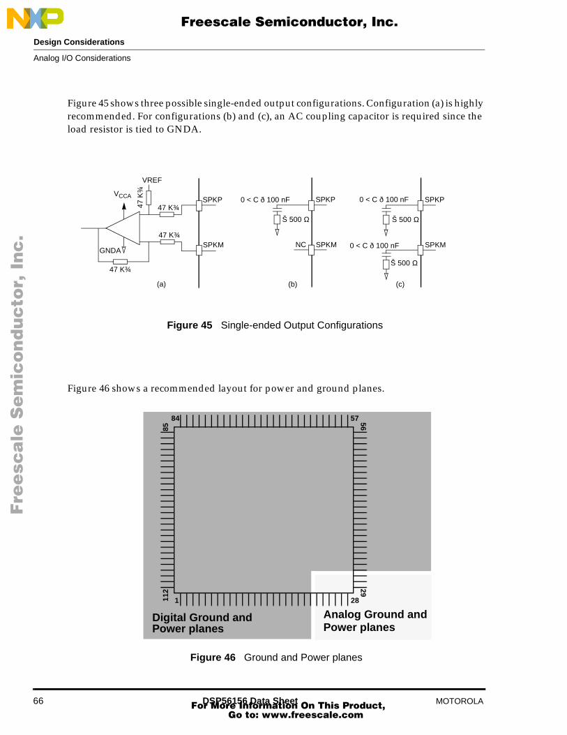
Design Considerations
66 DSP56156 Data Sheet MOTOROLA
Figure 45 shows three possible single-ended output configurations. Configuration (a) is highly recommended. For configurations (b) and (c), an AC coupling capacitor is required since the load resistor is tied to GNDA.
Figure 46 shows a recommended layout for power and ground planes.
Figure 46 Ground and Power planes
Š 500 Ω
SPKP
SPKM
Š 500 Ω47 K¾
47 K¾
47 K¾
VREF
47 K
¾
SPKP
SPKM
SPKP
SPKM
Š 500 Ω
0 < C ð 100 nF
NC
(a) (b) (c)
-
+
VCCA
GNDA
0 < C ð 100 nF
0 < C ð 100 nF
Figure 45 Single-ended Output Configurations
1 28
84 57 5629
112
85
Analog Ground and Power planes
Digital Ground and Power planes
Analog I/O Considerations
Fre
esc
ale
Se
mic
on
du
cto
r, I
Freescale Semiconductor, Inc.
For More Information On This Product, Go to: www.freescale.com
nc
...
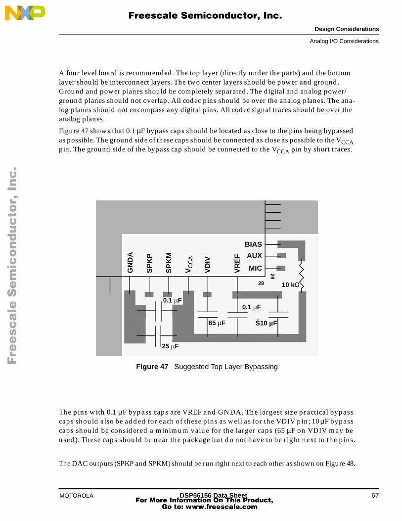
Design Considerations
MOTOROLA DSP56156 Data Sheet 67
A four level board is recommended. The top layer (directly under the parts) and the bottom layer should be interconnect layers. The two center layers should be power and ground. Ground and power planes should be completely separated. The digital and analog power/ground planes should not overlap. All codec pins should be over the analog planes. The ana-log planes should not encompass any digital pins. All codec signal traces should be over the analog planes.
Figure 47 shows that 0.1 µF bypass caps should be located as close to the pins being bypassed as possible. The ground side of these caps should be connected as close as possible to the VCCA pin. The ground side of the bypass cap should be connected to the VCCA pin by short traces.
Figure 47 Suggested Top Layer Bypassing
The pins with 0.1 µF bypass caps are VREF and GNDA. The largest size practical bypass caps should also be added for each of these pins as well as for the VDIV pin; 10 µF bypass caps should be considered a minimum value for the larger caps (65 µF on VDIV may be used). These caps should be near the package but do not have to be right next to the pins.
The DAC outputs (SPKP and SPKM) should be run right next to each other as shown on Figure 48.
28
29G
ND
A
SP
KP
SP
KM
VC
CA
BIAS
AUX
MIC
0.1 µF0.1 µF
Š10 µF
25 µF
VD
IV
VR
EF
65 µF
10 kΩ
Analog I/O Considerations
Fre
esc
ale
Se
mic
on
du
cto
r, I
Freescale Semiconductor, Inc.
For More Information On This Product, Go to: www.freescale.com
nc
...

Design Considerations
68 DSP56156 Data Sheet MOTOROLA
Figure 48 Suggested Bottom Layer Routing
The output should be used differentially if at all possible. Analog signal traces should be shielded by running traces connected to analog ground next to them. Unused board area on both interconnect levels should be copper filled and connected to analog ground. The copper fill is only shown on this page for clarity and simplicity. The ADC input anti-aliasing should be done with respect to VREF.
Figure 49 presents four options for good power supply connections.
28
29GN
DA
SP
KP
SP
KM
VC
CA
0.25 µF
47 kΩ
47 kΩ
Copper Fill of unused board spaceshould be connected to the analog ground plane.
BIAS
AUX
MIC
VD
IV
VR
EF
47 kΩ
1nF
47 kΩ
5.6 kΩ
MIC IN
SPK OUT
Analog I/O Considerations
Fre
esc
ale
Se
mic
on
du
cto
r, I
Freescale Semiconductor, Inc.
For More Information On This Product, Go to: www.freescale.com
nc
...

Design Considerations
MOTOROLA DSP56156 Data Sheet 69
Figure 49 Four Possible Power Supply Connections
28
29
GN
DA
SP
KP
SP
KM
VC
CA
AUXMIC
VR
EF
VD
IV
Ideal Choice — Two separate power supplies. Ground planes connected with a single trace as close as possible to the VCCA pin on the codec.
GN
DA
SP
KP
SP
KM
VC
CA
Second Choice — One power supply. Two regulators, one for the digital supply, one for the analog supply. Ground planes connected with a 10 ¾ resistor as close as possible to the VCCA pin on the codec.
10Ω
Voltage Regulator
BIAS
28
29
AUXMIC
VR
EF
VD
IV
BIAS
Voltage Regulator
Third Choice — One power supply. One regulator for the analog supply. Digital sup-plies driven directly by voltage source. Ground planes connected with a 10 ¾ resistor as close as possible to the VCCA pin on the codec.
10Ω
Fourth Choice — One power supply. Ground planes connected at source. Ground planes connected with a 10 ¾ resistor as close as pos-sible to the VCCA pin on the codec.
28
29
GN
DA
SP
KP
SP
KM
VC
CA
AUXMIC
VR
EF
VD
IV
BIAS
10Ω
28
29
GN
DA
SP
KP
SP
KM
VC
CA
AUXMIC
VR
EF
VD
IVBIAS
Voltage Regulator
Analog I/O Considerations
Fre
esc
ale
Se
mic
on
du
cto
r, I
Freescale Semiconductor, Inc.
For More Information On This Product, Go to: www.freescale.com
nc
...
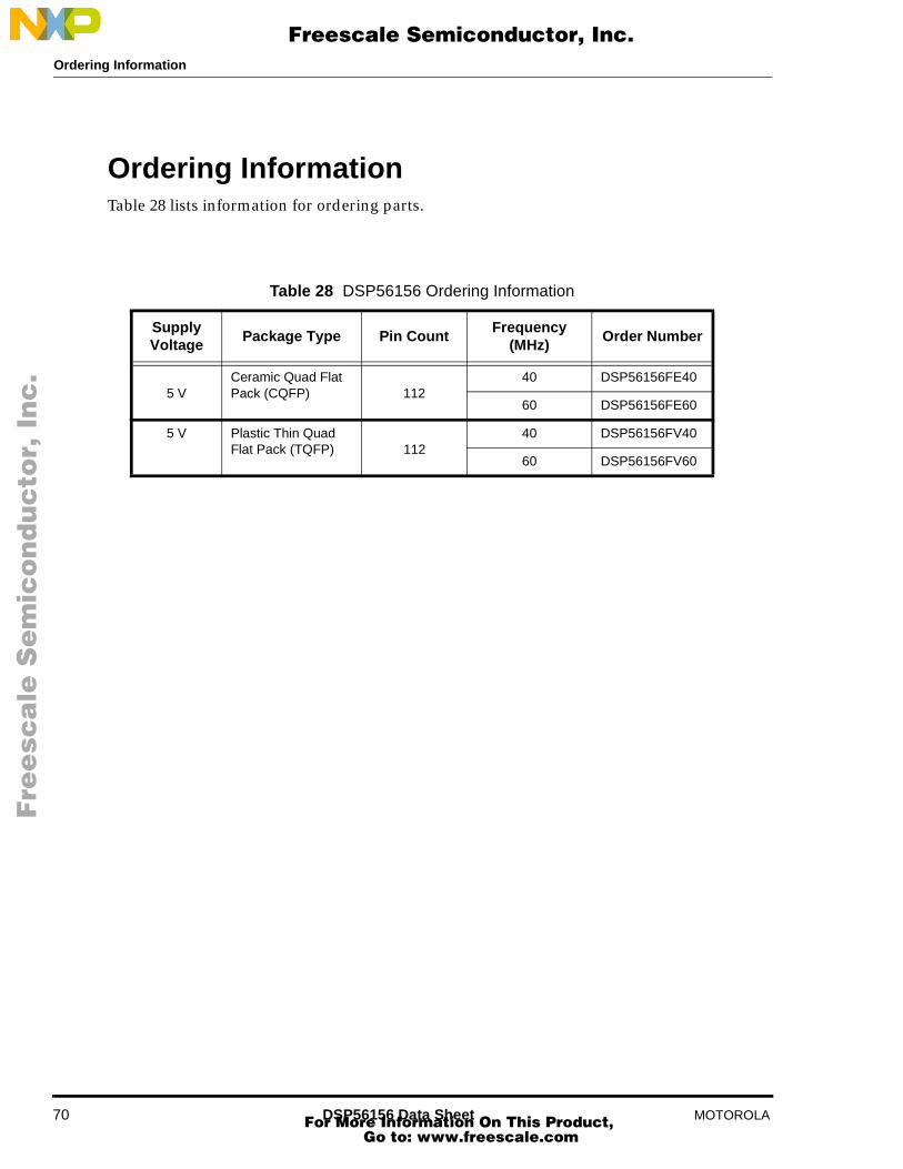
Ordering Information
70 DSP56156 Data Sheet MOTOROLA
Ordering InformationTable 28 lists information for ordering parts.
Table 28 DSP56156 Ordering Information
Supply Voltage
Package Type Pin CountFrequency
(MHz)Order Number
5 VCeramic Quad Flat Pack (CQFP) 112
40 DSP56156FE40
60 DSP56156FE60
5 V Plastic Thin Quad Flat Pack (TQFP) 112
40 DSP56156FV40
60 DSP56156FV60
Fre
esc
ale
Se
mic
on
du
cto
r, I
Freescale Semiconductor, Inc.
For More Information On This Product, Go to: www.freescale.com
nc
...

MOTOROLA
Motorola reserves the right to make changes without further notice to any products herein to improve reliability, function or design. Motorola does not assumeany liability arising out of the application or use of any product or circuit described herein; neither does it convey any license under its patent rights nor the rightsof others. Motorola products are not designed, intended, or authorized for use as components in systems intended for surgical implant into the body, or otherapplications intended to support or sustain life, or for any other application in which the failure of the Motorola product could create a situation where personalinjury or death may occur. Should Buyer purchase or use Motorola products for any such unintended or unauthorized application, Buyer shall indemnify andhold Motorola and its officers, employees, subsidiaries, affiliates, and distributors harmless against all claims, costs, damages, and expenses, and reasonableattorney fees arising out of, directly or indirectly, any claim of personal injury or death associated with such unintended or unauthorized use, even if such claimalleges that Motorola was negligent regarding the design or manufacture of the part. Motorola and M are registered trademarks of Motorola, Inc. Motorola, Inc.is an Equal Opportunity/Affirmative Action Employer.
Literature Distribution Centers:USA: Motorola Literature Distribution; P.O. Box 20912; Phoenix, Arizona 85036.EUROPE: Motorola Ltd.; European Literature Center; 88 Tanners Drive, Blakelands, Milton Keynes, MK14 5BP, England.JAPAN: Nippon Motorola Ltd.; 4-32-1, Nishi-Gotanda, Shinagawa-ku, Tokyo 141 Japan.ASIA-PACIFIC: Motorola Semiconductors H.K. Ltd.; Silicon Harbor Center, No. 2 Dai King Street, Tai Po Industrial Estate, Tai Po, N.T.,
Hong Kong.
Fre
esc
ale
Se
mic
on
du
cto
r, I
Freescale Semiconductor, Inc.
For More Information On This Product, Go to: www.freescale.com
nc
...