Introduction to Digital Circuit Introduction to Digital Circuit Design
Upload
amit-agrawalCategory
view
114download
7description

SYLLABUS
Subject Subject Name Teaching Scheme Credits Assigned
code Theory Practical Tut. Theory TW/Pract Tut Total SEITC304 Analog and 04 02 - 04 01 - 05
Digital Circuits
Subject Subject Examination Scheme
code Name Theory Marks TW Pract Oral Total
Internal Assessment End
Semester
Exam
SEITC304 Analog and Test1 Test2 Average of
Digital Test1 and
Circuits Test2
20 20 20 80 25 25 - 150
Course Objective: 1) To provide concepts that underpins the disciplines of Analog circuits, digital electronics
and Microprocessor systems. 2) To provide the concept of various components
3) To provide basic knowledge of designing Analog and digital circuits
Course outcomes: 1) Knowledge and Awareness of various components. 2) Design of stable analog circuits. 3) Circuit simulation.
4) Binary and hexadecimal calculations and conversions. 5) Design of combinational and sequential circuits.
6) Translate real world problems into digital logic formulations. 7) Awareness in Design of digital systems and concepts of Microprocessor and Microcontroller systems.
Detailed Syllabus:
Module Detailed Contents Hours
Voltage Regulator and components: Zener diode. Series and Shunt
1 Regulator. Regulator ICs 78XX, IC 79XX.Light Emitting diode(LED),
Schottky diode, Varactor diode, power diode, Photodiodes, Liquid- 06
crystal Displays, Solar cells, Thermistor.
2 Biasing of BJT: DC operating point, BJT characteristics & parameters, 08
University of Mumbai, Information Technology (Second Year – Sem. III &IV) Revised Course (Rev-2012)

all biasing circuits, analysis of above circuits and their design, variation
of operation point and its stability. Differential Amplifier, constant
current source, current mirror. Introduction to FET and comparison with
BJT.
Operational Amplifiers and linear applications: Block diagram
representation, Ideal Op-amp, Equivalent circuit, Open-loop
configuration, Transfer characteristics. Op-amp with negative feedback,
3 Frequency response. Op-amp IC 741 specifications. Basic op-amp
10
applications: Adder, Scalar, Subtractor, Difference amplifier, I-V
converter, V-I converters, Integrator, Differentiator, Instrumentation
amplifier using 2 and 3 op-amp stages. IC 555 Timer, Astable, and
Monostable Multivibrator.
Number Systems and Codes: Binary, Octal, Decimal and Hexadecimal
4 number Systems and their conversion, Binary Addition and Subtraction 04
, Gray Code, BCD Code, Excess-3 code, ASCII Code.
Boolean Algebra and Logic Gates: Theorems and Properties of Boolean
Algebra, Standard SOP and POS form, Reduction of Boolean functions
using Algebric method, K -map method (2,3,4 Variable).
5 Basic Digital Circuits: NOT,AND,OR,NAND,NOR,EX-OR,EX-NOR 04
Gates.
Combinational Logic Design: Introduction, Half and Full Adder, Half
6 and Full Subtractor, Four Bit Binary Adder, One digit BCD Adder, code
06
conversion, Multiplexers and Demultiplexers, Decoders, 4-bit
Magnitude Comparator IC 7485 and ALU IC74181.
Sequential Logic Design: Flip Flops: SR, D, JK, JK Master Slave and T
Flip Flop, Truth Tables and Excitation Tables, Flip-flop conversion.
Counters: Design of Asynchronous and Synchronous Counters, Modulo
7 Counters, UP- DOWN counter .IC 74193 06
Shift Registers: Shift Register IC 7496 , SISO, SIPO,PIPO,PISO,
Bidirectional Shift Register , Universal Shift Register, Ring and Johnson
Counter.
Introduction to VHDL: Introduction , Library, Entity, Architecture,
8 Modeling Styles, Concurrent and sequential statements, Data objects 04
and Data types, attributes. Design Examples for combinational circuits.
TERMWORK MARKS: 1. Attendance (Theory and Practical) - 05
2. Laboratory work (Experiments and Journal) -15 3. Assignments -05
The final certification and acceptance of TW ensures the satisfactory performance of Laboratory Work and Minimum Passing in the term work.
University of Mumbai, Information Technology (Second Year – Sem. III &IV) Revised Course (Rev-2012)

LABORTARY WORK:
1. Laboratory work should consist of at least 10 Experiments.
The Experiments should be based on following topics (Any Ten):
1) Zener diode as Regulator.
2) BJT Biasing Method.
3) OP-amp as Inverting and Non-inverting amplifier.
4) Applications of Op-amp.
5) IC 555 as astable Multivibrator.
6) Simulation of any circuit using Pspice.
7) Logic Gates.
8) Code Conversion.
9) Multiplexer, Demultiplexer.
10) Flip-flops using gates and ICs.
11) Design of Sequential circuits.
12) VHDL for Combinational logic.
Text Books: 1. Robert L. Boylestad, Louis Nashelsky, “Electronic devices and circuit Theory”, PHI 2. Ramakant A. Gaikwad, “Op-amp and linear Integrated circuits”, PHI 3. R. P. Jain, “Modern Digital Electronics”, Tata McGraw Hill. 4. M. Morris Mano, “Digital Logic and computer Design”, PHI. 5. J. Bhasker.“ VHDL Primer”, Pearson Education Reference Books: 1. Martin s. Roden, Gordon L. Carpenter, William R. Wieserman “Electronic Design-From Concept
to Reality”, Shroff Publishers and Distributors. 2. D.roy Choudhury,shail B.jain, “Linear integrated Circuits”, New age International Publisher. 3. Subrata Ghosal, ”Digital Electronics”, Cengage Learning. 4. Anil K. Maini, “Digital Electronics Principles and Integrated Circuits”, Wiley India 5. Donald p Leach, Albert Paul Malvino, “Digital principles and Applications”, Tata McGraw Hill.
University of Mumbai, Information Technology (Second Year – Sem. III &IV) Revised Course (Rev-2012)

Theory Examination :
Question paper will comprise of 6 questions, each carrying 20
marks. Total 4 questions need to be solved.
Q.1 will be compulsory, based on entire syllabus wherein sub questions of 2 to 3 marks will
be asked. Remaining question will be randomly selected from all the modules.
Weightage of marks should be proportional to number of hours assigned to each module. University of Mumbai, Information Technology (Second Year – Sem. III &IV) Revised Course (Rev-2012)

Module 4: Number Systems and Codes
Syllabus : Binary, Octal, Decimal and Hexadecimal number Systems and their conversion, Binary
Addition and Subtraction , Gray Code, BCD Code, Excess-3 code, ASCII Code.
Introduction:
Signals: Signal is defined as a physical quantity, which contains some information and which is a
function of one or more independent variables.
Comparison between Analog & Digital Signals:
Sr.
No
.
Parameter
s
Analog Signal Digital Signal
1. Definition Signal having continuous values Signal which has only a finite no. of
distinct values
2. Diagram
3. No. of
values
Infinite Finite
4. Nature Continuous Discrete
5. Sources Signal generators, Transducers etc. Computers, A/D Convertors etc.
6. Examples Temperature, Pressure, Distance, Sound,
Brightness, Voltage, Current, Power etc
Binary, Octal, Hexadecimal signals
Systems: A system or circuit is defined as the physical device or group of devices or algorithm which
performs the required operations on the signal applied at its input.
Comparison between Analog & Digital Systems:
Sr. No. Parameters Analog System Digital System
1. Definition Circuits that processes the
analog signals
Circuits that processes the
digital signals
2. Type of display Analog meters i.e pointers Digital Display using LED &
LCD
3. Accuracy Less More
4. Design
Complexity
More Less
5. Memory Not present Present
6. Storage of Not Possible Possible

Information
7. Effect of Noise More Less
8. Versatility Less More
9. Distortion More Less
10. Effect of
temperature and
ageing on
performance
More
Less
11. Communication
between systems
Difficult Simple
12. Examples Filters, Amplifiers, Signal
Generators, Power Supply,
Disc Players, T.V Receivers
Counters, Registers,
Microprocessors, Computers
etc.
Number Systems and their Conversion:
A. DecimalNumber System :
We are most familiar with the positional, base-10 (decimal), Hindu-Arabic numeral system:
0,1,2,3,4,5,6,7,8,& 9,Least significant digit, to the right, assumes its own value.
As we move to the left, the value is multiplied by the base.
The „Base‟ or „Radix‟ of a number system is defined as the number of different digits which
can occur in each position in the number system.
Each position represents a specific power of the base (10). For example, the decimal number
1234 consists of the digit 4 in the units position, 3 in the tens position, 2 in the hundreds
position, and 1 in the thousands position, and its value can be written as;
(1x1000)+ (2x100)+ (3x10)+ (4xl) = 1000 + 200 + 30 + 4 = 1234.
The following are 3 important characteristics of a number system having positional notation
(place value) :
1. Base / Radix = No. of digits.
2. Largest degree one less than the base.
3. Each digit is multiplied by the base/radix raised to an appropriate power depending upon
the digit position to get its place value.
B. Binary Number System :
The binary number system is also a positional notation numbering system, but in this case, the
base is not ten, but is instead two.
Each digit position in a binary number represents a power of two.
So, when we write a binary number, each binary digit is multiplied by an appropriate power of 2
based on the position in the number:
For example:
101101 = 1 x 25 + 0 x 24 + 1 x 23 + 1 x 22 + 0 x 21 + 1 x 20
= 1 x 32 + 0 x 16 + 1 x 8 + 1 x 4 + 0 x 2 + 1 x 1
= 32 + 8 + 4 + 1
= (45)10
In the binary number system, there are only two possible values that can appear in each digit
position rather than the ten that can appear in a decimal number.
Only the numerals 0 and 1 are used in binary numbers.

The term „bit‟ is a contraction of the words „binary‟ and „digit‟, and when talking about binary
numbers the terms bit and digit can be used interchangeably.
When talking about binary numbers, it is often necessary to talk of the number of bits used to store
or represent the number.
Conversion of Binary to Decimal:
Converting a number from binary to decimal is quite easy. All that is required is to find the decimal
value of each binary digit position containing a 1 and add them up.
For example:
1. Convert 101102 to decimal.
1 0 1 1 0
\ \ \___________1 x 21 = 2
\ \____________1 x 22 = 4
\_______________1 x 24 = 16
22
2. Convert 110112 to decimal
1 1 0 1 1
\ \ \ \_________1 x 20 = 1
\ \ \__________1 x 21 = 2
\ \_____________1 x 23 = 8
\______________1 x 24 = 16
27
Conversion of Decimal to Binary:
It involves using successive division by the radix until the dividend reaches 0. At each division, the
remainder provides a digit of the converted number, starting with the least significant digit.
An example of the process:
1. Convert 3710 to binary
37 / 2 = 18 remainder 1 (least significant digit)
18 / 2 = 9 remainder 0
9 / 2 = 4 remainder 1
4 / 2 = 2 remainder 0
2 / 2 = 1 remainder 0
1 / 2 = 0 remainder 1 (most significant digit)
The resulting binary number is: 100101
2. Convert 9310.8125 to binary
93 / 2 = 46 remainder 1 (least significant digit) 0.8125 × 2 = 1.625 1
46 / 2 = 23 remainder 0 0.625 × 2 = 1.25 1
23 / 2 = 11 remainder 1 0.25 × 2 = 0.5 0
11 / 2 = 5 remainder 1 0.5 × 2 = 1.0 1
5 / 2 = 2 remainder 1
2 / 2 = 1 remainder 0
1 / 2 = 0 remainder 1 (most significant digit)
The resulting binary number is: 1011101. 1101
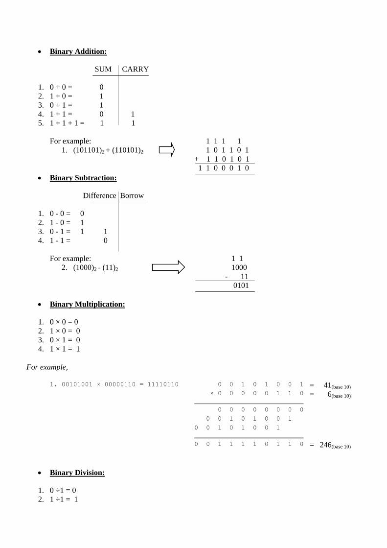
Binary Addition:
SUM CARRY
1. 0 + 0 = 0
2. 1 + 0 = 1
3. 0 + 1 = 1
4. 1 + 1 = 0 1
5. 1 + 1 + 1 = 1 1
For example: 1 1 1 1
1. (101101)2 + (110101)2 1 0 1 1 0 1
+ 1 1 0 1 0 1
1 1 0 0 0 1 0
Binary Subtraction:
Difference Borrow
1. 0 - 0 = 0
2. 1 - 0 = 1
3. 0 - 1 = 1 1
4. 1 - 1 = 0
For example: 1 1
2. (1000)2 - (11)2 1000
- 11
0101
Binary Multiplication:
1. 0 × 0 = 0
2. 1 × 0 = 0
3. 0 × 1 = 0
4. 1 × 1 = 1
For example,
1. 00101001 × 00000110 = 11110110 0 0 1 0 1 0 0 1 = 41(base 10) × 0 0 0 0 0 1 1 0
= 6(base 10)
0 0 0 0 0 0 0 0 0 0 1 0 1 0 0 1
0 0 1 0 1 0 0 1
0 0 1 1 1 1 0 1 1 0 = 246(base 10)
Binary Division:
1. 0 ÷1 = 0
2. 1 ÷1 = 1

For example,
00101010 ÷ 00000110 =
00000111 1 1 1 = 7(base 10)
1 1 0 ) 0 0 1 10 1 0 1 0 = 42(base 10)
- 1 1 0 = 6(base 10)
1 borrows
1 0 10 1
- 1 1 0
1 1 0
- 1 1 0
0
C. Octal Number System :
Then the main characteristics of an Octal Numbering System is that there are only 8 distinct
counting digits from 0 to 7 with each digit having a weight or value of just 8 starting from the least
significant bit (LSB).
Conversion of Octal to Decimal:
To change this number to base 8, multiply each placeholder by the amount its location represents and
add them
For example:
1. (53701)8 = 5 x 84 + 3 x 8
3 + 7 x 8
2 + 0 x 8
1 + 1 x 8
0
= (5 x 4096) + (3 x 512) + (7 x 64) + (0 x 8) + (1 x 1)
= 20,480 + 1536 + 448 + 0 + 1
= (22,46510)10
Conversion of Decimal to Octal:
It involves using successive division by the radix until the dividend reaches 0. At each division, the
remainder provides a digit of the converted number, starting with the least significant digit.
An example of the process:
1. Convert (3000.45)10to octal
3000 / 8 = 375 remainder 0 (least significant digit) 0.45 × 8 = 3.6 3
375 / 8 = 46 remainder 7 0.6 × 8 = 4.8 4
46 / 8 = 5 remainder 6 0.8 × 8 = 6.4 6
5 / 8 = 0 remainder 5 0.4 × 8 = 3.2 3
The resulting Octal number is: (5670. 3463)8
Conversion of Octal to Binary:
To convert octal to binary, represent octal number in 3 bits of binary.
For example:
1. (123.567)8 (001 010 011.101 110 111)2

Conversion of Binary to Octal:
To convert binary to octal, group the 3 binary bits as 3-binary bits gives equivalent 8 state.
For example:
1. (001 010 011.101 110 111)2 (123.567)8
D. Hexadecimal Number System :
The hexadecimal number system (AKA hex) is a base 16 notation. It is the most popular large-base
system for representing binary numbers.
Values in MIDI implementation charts are often expressed as hexadecimal numbers.
Each symbol represents 4-bits, that can take one of 16 different values: the values 0-9 are
represented by the digits 0-9, and the values 10-15 are represented by the capital letters A-F.
Conversion of Hexadecimal to Decimal:
To change this number to base 16, multiply each placeholder by the amount its location represents and add
them
For example:
1. (10F.2F)16 = 10 x 162 + F x 16
0 + 2 x 16
-1 + F x 16
-2
(10F.2F)H = (10 x 256) + (15 x 1) + (2 x 0.0625) + (15 x 0.00390625)
= 2560 + 15 + 0.125 + 0.0586
= (2575.1836)10
Conversion of Decimal to Hexadecimal:
It involves using successive division by the radix (16) until the dividend reaches 0. At each division, the
remainder provides a digit of the converted number, starting with the least significant digit.
An example of the process:
1. Convert (2003.31)10to octal
2003 / 16 = 3 remainder 3 (least significant digit) 0.31 × 16 = 4.96 4
125 / 16 = 7 remainder (13)D 0.96 × 16 = 15.36 (15)D
7 / 16 = 5 remainder 7 0.36 × 16 = 5.765 5
The resulting hexadecimal number is: 7D3.4F5
Conversion of Hexadecimal to Binary:
To convert hexadecimal to binary, represent hexadecimal number in 4 bits of binary.
For example:
1. (1A3.BA)8 (0001 1010 0011.1011 1010)2
Conversion of Binary to Hexadecimal:
To convert binary to hexadecimal, group the 4 binary bits as 4-binary bits gives equivalent 16 state.
For example:
1. (1100101011)2 (0011 0010 1011)2 (123.567)8

Conversion of Hexadecimal to Octal:
To convert hexadecimal to Octal, follow the following 2 steps:
I. Represent hexadecimal number in 4 bits of binary and then
II. Convert that binary number to Octal
For example:
1. (1A3.BA)H (0001 1010 0011.1011 1010)2 (000 110 100 011.101 110 100)2 (0643.564)8
Binary Addition and Subtraction Using Compliment Method:
• Need of Compliment :
Complements are used in digital computers to simplify the subtraction operation and for
logical manipulation. Subtraction of numbers in a computer is complicated & expensive in
terms of circuit, especially for repeated borrowing for one column to another. Borrowing
circuit is quite complex and expensive. Thus, by using compliment technique subtraction is
done by addition technique, thus reducing cost of the system.
• Types of Compliment :
1. Radix – 1 compliment
2. Radix compliment
• Binary Number System :
For this system Radix = 2
So there are two techniques;
1. 2 – 1 = 1‟s compliment
2. 2‟s compliment
1’s Compliment :
• The 1's complement of a number is found by changing all 1's to 0's and all 0's to 1's. This is called
as taking complement or 1's complement.
Example of 1's Complement is as follows:
Circuit to obtain 1‟s Compliment

2’s Compliment :
• The 2's complement of binary number is obtained by adding 1 to the Least Significant Bit (LSB) of
1's complement of the number.
• 2's complement = 1's complement + 1
Example of 2's Complement is as follows.
Circuit to obtain 2‟

Representation of Signed and Unsigned Numbers :
Subtraction Using Compliment :
For Subtraction, make the Subtrahend and Minuend of equal digits by;
a. Adding zeros to the integer in MSB side and
b. Adding zeros to the fraction in LSB side.
Using 1’s Compliment : • Steps are as follows:
1. Compliment the Subtrahend (Number to be subtracted).
2. Add the complement with Minuend (from the number to be subtracted)
3. Delete the higher order carry, if any, and ADD to the sum obtained in Step 2.
4. If No Carry is generated (i.e. when a larger number is subtracted from a smaller
number), then Re-complement the sum and attach a negative sign, to obtain a result.
Example:
1. Subtract (101011)2 from (111001)2 using 1‟s compliment
Sol:
111001
+ 010100 1‟s compliment of 101011
(1) 001101
+ 1
001110 Final answer

2. Subtract (111001)2 from (101011)2 using 1‟s compliment method
Sol.
101011
+ 000110 1‟s compliment of 111001
110001 No carry generated so answer in 1‟s compliment form
-001110 answer in true form
Using 2’s Compliment : • Like 1‟s compliment subtraction in 2‟s compliment subtraction, the subtraction is
accomplished by only addition. For subtraction of two numbers we have two cases:
• Subtraction of smaller numbers from larger number:
1. Determine the 2‟s compliment of the smaller number.
2. Add the 2‟s compliment to the larger number.
3. Discard the carry.
Example: Subtract (101011)2 from (111001)2 using 2‟s compliment method
Sol.
111001
+ 010101 2‟s compliment of 101011
discard (1) 001110 Final answer
• Subtraction of larger number from smaller number method:
1. Determine the 2‟s compliment of the larger number.
2. Add the 2‟s compliment to the smaller number.
3. Answer is in 2‟s compliment form. To get the answer in true form take the 2‟s compliment
and assign negative sign to the answer.
Example: Subtract (111001)2 from (101011)2 using 1‟s compliment method
Sol.
101011
+ 000111 2‟s compliment of 111001
110010 answer in 2‟s compliment form
- 001110 answer in true form
Gray Code • An n-bit Gray code, also called the reflected binary code, is an ordering of the 2 n-strings of length n over
{0, 1} such that every pair of successive strings differ in exactly one position.
• Gray code is non-weighted code.
• As only one bit changes at a time, the Gray Code is called “Unit Distance Code”.
• It‟s also called as “Cyclic Code”.

Some Gray Codes possesses Reflective Property
Application
Shaft Position Encoder produces a code word which represents the angular position of the shaft.
Pattern for Binary Code Pattern for Gray Code
Can lead to an error: 001 011 010
Converting Gray Code to Binary Code :
The bits of Gray code words are numbered from right to left, from 0 to n-1.
Bit i is 0 if bits i and i+1 of the corresponding binary code word are the same, else bit i is 1
When i+1 = n, bit n of the binary code word is considered to be 0
The most significant bit (MSB) in Gray is taken directly from the MSB in binary. The rest
of the Gray bits comes from a xor operation between the precedent binary bit (b(i-1)) and
the current binary bit (b(i)). As shown in the figure above:
• g(1) = b(1)

• g(2) = b(1) xor b(2)
• g(3) = b(2) xor b(3)
• g(4) = b(3) xor b(4)
• g(5) = b(4) xor b(5)
The xor operation produces a 1 if the bits are different, and produces a 0 if the bits are
equal. So, a binary „11101‟ becomes a „10011‟ in Gray.
Converting Binary Code to Gray Code :
Scan the Gray code word from left to right
All the bits of the binary code are the same as those of the Gray code until the first 1 is
encountered, including the first 1.
1‟s are written until the next 1 is encountered, in which case a 0 is written.
0‟s are written until the next 1 is encountered, in which case a 1 is written.
The most significant bit (MSB) in binary is taken directly from the MSB in Gray. The rest
of the binary bits comes from a xor operation between the precedent binary bit (b(i-1)) and
the current Gray bit (g(i)). In the case shown in the figure above:
• b(1) = g(1)
• b(2) = b(1) xor g(2)
• b(3) = b(2) xor g(3)
• b(4) = b(3) xor g(4)
• b(5) = b(4) xor g(5)
BCD Code Binary coded decimal (BCD) is a weighted code that is commonly used in digital systems when it is
necessary to show decimal numbers such as in clock displays.

We will be studying 8-4-2-1 BCD code.
Relation between Decimal- Binary and BCD Code :
BCD Addition:
Assume that two 4-bit BCD numbers A and B are being added. Then the 3 cases to be
considered namely;
Sum ≤ 9, Carry = 0 Sum ≤ 9, Carry = 1 Sum > 9, Carry = 0
Answer is Correct Add 6 to the sum to Add 6 to the sum to get
get correct answer correct answer
Example:
1. Add (45)10 + (33)10 = (78)10
BCD
(45)10 0100 0101
(33)10 + 0011 0011
(78)10 0111 1000
2. Add (59)10 + (38)10 = (97)10
BCD 1111
(59)10 0101 1001
(38)10 + 0011 1000
1001 0001
+ 0110 Carry is generated
(97)10 1001 0111
3. Add (47)10 + (35)10 = (82)10
BCD
(47)10 0100 0111
(35)10 + 0011 0101
0111 1100 No.is greater than 9
+ 1 0110
(82)10 1000 0010

EXCESS – 3 Code EXCESS – 3 is also called as XS-3 code.
It is non-weighted code used to express decimal number.
Below table shows that XS-3 code can be obtained using 8-4-2-1 BCD code.
Example:
1. Convert (247.6)10 into XS-3 code
BCD XS-3
Sol : (247.6)10 0010 0100 0111 . 0110 0101 0111 1010 . 1001
ASCII Code • American Standard Code for Information Interchange (ASCII) pronounced "askee".
• ASCII is a code for alphanumeric characters and control characters.
• In its original form, ASCII encoded 128 characters and symbols using 7-bits. The first 32 characters are
control characters, that are based on obsolete teletype requirements, so these characters are generally
assigned to other functions in modern usage.
• Figure below shows the ASCII table

Module 5: Boolean Algebra and Logic Gates
Syllabus : Theorems and Properties of Boolean Algebra, Standard SOP and POS form, Reduction of
Boolean functions using Algebric method, K -map method (2,3,4 Variable).
Basic Digital Circuits: NOT, AND, OR, NAND, NOR, EX-OR, EX-NOR Gates.
Introduction:
Digital electronic systems manipulate binary information.
To design such systems we need a convenient mathematical framework
– useful systems are often too complicated to keep in our head
– Boolean algebra provides this framework
Points in a circuit are represented by Boolean Variables
Boolean algebra allows us to specify relationships between Boolean variables
Hence Boolean algebra can be used as a design tool for digital electronic circuits
Boolean algebra is an algebra that deals with binary variables and logic operations.
Boolean variables take the value either 0 or 1 only
– if a variable doesn't have the value 0, then it must have the value 1
– if a variable doesn't have the value 1, then it must have the value 0
In digital electronics:
– Boolean 0 and 1 correspond to the binary 0 and 1
In logic:
– 1 and 0 are sometimes called true and false
We use symbols to represent Boolean variables
– just like with ordinary algebra
– eg: A, B, C, X, Y, Z, etc
– typically a single character
– typically upper case
Three Logic operations: AND, OR, NOT
Operations are defined on the values "0" and "1" for each operator.
BASIC GATES:
Sr.
No. Parameter AND OR NOT
1. Denoted
by Dot (·) Plus (+)
overbar ( ¯ ),
a single quote mark (') after, or
(~) before the variable.
2. Boolean
Expression Y =A ∙ B Y =A + B Y =A or À or ~A
3. Logical
Operations Multiplication Addition Inversion
4.
IC
Standard
Package
7408 7432 7404

5. Truth
Table
6. Switch
Diagram
7.
Gate
Represen-
tation
8. Waveform
UNIVERSAL GATES:
Sr.
No. Parameter NAND NOR
1. Combination of AND + NOT OR + NOT
2. Denoted by Dot (·) Plus (+)
3. Boolean
Expression Y = A ∙ B Y = A + B
4. Logical
Operation NOT AND NOT OR
5. IC Standard
Package IC 7400 IC 7402
6. Truth Table

7. Switch Diagram
8. Gate
Representation
9. Waveform
DERIVED GATES:
Sr.
No. Parameter EX-OR EX-NOR
1. Denoted by
+
2. Boolean
Expression Q = X ⊕ Y = X Y’ + X’ Y X ∙ Y = X Y + X’ Y’ = (X ⊕ Y)’
3. Logical
Operation Addition / Subtraction NOT EXOR
4. IC Standard
Package IC 7486 IC 74266
5. Truth Table
6. Gate
Representation
7. Waveform

BOOLEAN LAWS:
VERIFICATION OF De – Morgan’s Theorems:
1. A ∙ B = A + B
This theorem states that the complement of a product is equal to addition of the
complements.
Truth Table : Circuit Diagram :

2. A + B = A ∙ B
This theorem states that the complement of a sum is equal to product of the complements.
Truth Table : Circuit Diagram :
Example:
A. For the following Boolean expression, draw the logic circuit. Simplify the expression using
Boolean algebra and draw the simplified logic circuit.
1. AB + A(B + C) + B(B + C) = AB + AB + AC + BB + BC
= AB + AB + AC + B + BC
= AB + AC + B + BC
= AB + AC + B
= B + AC
2. A + AB = (A + AB) + AB
= (AA + AB) + AB
= AA +AB +AA +AB
= (A + A)(A + B)
= 1. (A + B)
= A + B

B. Applying De-Morgan’s Theorem, Prove that = (A + BC)(D + E + F)
L.H.S =
= (A + BC) (D (E + F))
= (A + BC) (D (E + F))
= (A + BC) (D + (E + F))
= (A + BC)(D + E + F)
= R.H.S
Hence, Proved
C. Write the Boolean equation for the given circuit. Using rules of Boolean algebra and
De-Morgan’s theorem simplify the equation and draw the simplified circuit.
Boolean Equation is:
F = A∙B + A∙B + B∙C
= A (B + B) + BC
= A ∙ 1 + BC
= A + BC
Simplified Circuit:

GATE CONVERSION USING ONLY NAND GATES
Y = A ∙ B
Sr.
No. OPERATION EQUATION LOGIC DIAGRAM
1. NOT Y = A = A ∙ A
2. AND Y = A∙B = A∙B
3. OR
Y = A + B
= A + B
= A ∙ B
4. NOR
Y = A + B
= A ∙ B
= A ∙ B
5. EX-OR
Y = A ⊕ B = A’B + AB’ = A’B + AB’ = (AB’) ∙ (A’B) = (A’B) ∙ (AB’)
6. EX-NOR
Y = A ʘ B
= A’B’ + AB
= A’B’ + AB
= (A’B’) ∙ (AB)
GATE CONVERSION USING ONLY NOR GATES
Y = A + B
Sr.
No. OPERATION EQUATION LOGIC DIAGRAM
1. NOT Y = A = A + A
2. AND
Y = A∙B = A∙B = A’ + B’

3. OR
Y = A + B
= A + B
4. NAND
Y = A ∙ B
= A + B
= A + B
5. EX-OR
Y = A ⊕ B = A’B + AB’ = A’B + AB’ = (AB’) ∙ (A’B) = (A’+B) ∙ (A +B’) = (A’+B) + (A +B’) =(A’+B) + (A +B’)
6. EX-NOR
Y = A ʘ B
= A’B’ + AB
=(A’+B) + (A +B’) =(A’+B) + (A +B’)
GENERAL DEFINATIONS
Literal: A Boolean variable in its complemented or un-complemented form is referred to as Literal.
Truth- Table: It consists of all possible combinations of the inputs and the corresponding state of
output of a logic gate.
Boolean Algebra: It is used to analyse and simplify the logic circuits. Since it relates with binary
numbers 1 & O so also called as “Binary” or “Logical” Algebra.
Boolean Expression: Relation between inputs and outputs of a gate can be expressed
mathematically by means of it.
Design o Digital Circuits
Example: Design the circuitry of the logic system to open the waste valve if and only if there is
good flame proven by the sensors.

Sol:
Truth-Table:
Logic Diagram:

Simplification:
Simplified Logic Diagram:

Standard and Canonical Forms
STANDARD FORMS OF BOOLEAN EXPRESSIONS
All Boolean expressions, regardless of their form, can be converted into either of two
standard forms:
1. the sum-of-products form or
2. the product-of sums form.
Standardization makes the evaluation, simplification, and implementation of Boolean
expressions much more systematic and easier.
The Sum-of-Products (SOP) Form
When two or more product terms are summed by Boolean addition, the resulting
expression is a sum-of-products (SOP).
Example : AB + BCD + AC
Implementation :
The Standard SOP Form
So far, you have seen SOP expressions in which some of the product terms do not
contain all of the variables in the domain of the expression.
For example, the expression A'BC' + AB'D + ABC'D' has a domain made up of the
variables A, B, C. and D. However, notice that the complete set of variables in the
domain is not represented in the first two terms of the expression; that is, D or D' is
missing from the first term and C or C' is missing from the second term.
A standard SOP expression is one in which all the variables in the domain appear in
each product term in the expression.
For example, A'BCD' + ABC'D + AB'CD is a standard SOP expression.
Converting Product Terms to Standard SOP:
Each product term in an SOP expression that does not contain all the variables in the
domain can be expanded to standard SOP to include all variables in the domain and
their complements.
As stated in the following steps, a nonstandard SOP expression is converted into
standard form using Boolean algebra rule - (A + A' = 1)
A variable added to its complement equals 1.
Following are the steps for conversion:

Step 1: Multiply each non-standard product term by a term made up of the sum of a missing
variable and its complement. This results in two product terms. As you know, you
can multiply anything by 1 without changing its value.
Step 2: Repeat Step 1 until all resulting product terms contain all variables in the domain in
either complemented or un-complemented form. In converting a product term to standard
form, the number of product terms is doubled for each missing variable.
Example
Convert the following Boolean expression into standard SOP form: AB'C + A'B' + ABC'D
Solution
The domain of this SOP expression A, B, C, D.
Take one term at a time.
The first term, AB'C, is missing variable D or D', so multiply the first term by (D +
D') as follows:
AB'C = AB'C(D + D') = AB'CD + AB'CD'
In this case, two standard product terms are the result.
The second term, A'B', is missing variables C or C' and D or D', so first multiply the
second term by C + C' as follows:
AB = A'B' (C + C') = A'B'C + A'B'C'
The two resulting terms are missing variable D or D', so multiply both terms by
(D + D') as follows:
A'B'C(D + D') + A'B'C' (D + D') = A'B'CD + A'B'CD' + A'B'C'D + A'B'C'D'
In this case, four standard product terms are the result.
The third term, ABC'D, is already in standard form. The complete standard SOP form
of the original expression is as follows:
AB'C + A'B' + ABC'D
= AB'CD + AB'CD' + A'B'CD + A'B'CD' + A'B'C'D + A'B'C'D' + ABC'D
The Product-of-Sums (POS) Form
A sum term was defined before as a term consisting of the sum (Boolean addition) of
literals (variables or their complements).
When two or more sum terms are multiplied, the resulting expression is a product-of-
sums (POS).
Some examples are
(A' + B)(A + B' + C)
(A + B' + C')( C + D' + E)(B + C + D)
(A + B')(A + B' + C)(A + C)
Implementation of a POS Expression simply requires ANDing the outputs of two or
more OR gates.
A sum term is produced by an OR operation and the product of two or more sum
terms is produced by an AND operation.

Figure shows for the expression (A + B)(B + C + D)(A + C). The output X of the
AND gate equals the POS expression.
The Standard POS Form
So far, you have seen POS expressions in which some of the sum terms do not
contain all of the variables in the domain of the expression.
For example, the expression
(A + B' + C) (A + B + D') (A + B' + C' + D)
has a domain made up of the variables A, B, C, and D.
Notice that the complete set of variables in the domain is not represented in first two
terms of the expression; that is, D or D' is missing from the first term and C or C' is
missing from the second term.
A standard POS expression is one in which all the variables in the domain appear in
each sum term in the expression.
For example,
(A' + B' + C + D)(A + B' + C + D)(A + B + C + D)
is a standard POS expression. Any nonstandard POS expression (referred to simply
as POS) can be converted to the standard form using Boolean algebra.
Converting a Sum Term to Standard POS
Each sum term in a POS expression that does not contain all the variables in the
domain can be expanded to standard form to include all variables in the domain and
their complements.
As stated in the following steps, a nonstandard POS expression is converted into
standard form using Boolean algebra - A∙ A = 0
Step 1. Add to each nonstandard product term a term made up of the product of the
missing variable and its complement. This results in two sum terms.
As you know, you can add 0 to anything without changing its value.
Step 2. Apply rule : A + BC = (A + B)(A + C)
Step 3. Repeat Step 1 until all resulting sum terms contain all variables in the domain
in either complemented or non-complemented form.
Example:
Convert the following Boolean expression into standard POS form:
(A' + B + C)(B' + C + D')(A + B' + C' + D)

Solution:
The domain of this POS expression is A, B, C, D. Take one term at a time.
The first term, A' + B + C, is missing variable D or D', so add DD' and apply
rule as follows:
A' + B + C = A' + B + C + DD' = (A' + B + C + D)(A' + B + C + D')
The second term, B' + C + D', is missing variable A or A', so add AA' and
apply rule as follows:
B' + C + D' = B' + C + D' + AA' = (A + B' + C + D')(A' + B' + C + D')
The third term, A + B + C' + D', is already in standard form.
The standard POS form of the original expression is as follows:
(A' + B + C)(B' + C + D')(A + B' + C' + D) =
(A' + B + C + D)(A' + B + C + D') (A + B' + C + D')(A' + B' + C + D') (A + B + C' + D')
Concept of Minterms and Maxterms
Each row of a truth table can be associated with a minterm, which is a product (AND) of all
variables in the function, in direct or complemented form.
A minterm has the property that it is equal to 1 on exactly one row of the truth table.
Here is the three-variable truth table and the corresponding minterms:
minterm
0 0 0
0 0 1
0 1 0
0 1 1
1 0 0
1 0 1
1 1 0
1 1 1
The subscript on the minterm is the number of the row on which it equals 1. (The row numbers are
obtained by reading the values of the variables on that row as a binary number.)
Minterms provide a way to represent any boolean function algebraically, once its truth table is
specified. The function is given by the sum (OR) of those minterms corresponding to rows where
the function is 1. By the minterm property, the OR will contain a term equal to 1 (making the
function 1) on exactly those rows where the function is supposed to be 1.
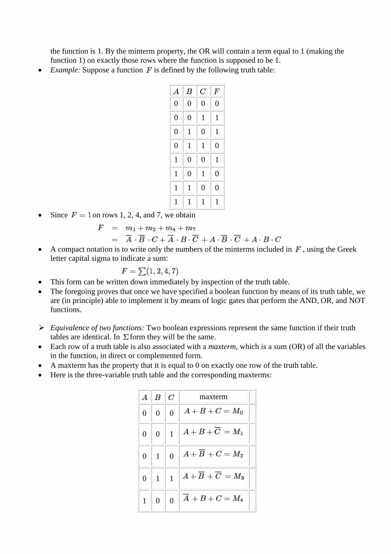
Example: Suppose a function is defined by the following truth table:
0 0 0 0
0 0 1 1
0 1 0 1
0 1 1 0
1 0 0 1
1 0 1 0
1 1 0 0
1 1 1 1
Since on rows 1, 2, 4, and 7, we obtain
A compact notation is to write only the numbers of the minterms included in , using the Greek
letter capital sigma to indicate a sum:
This form can be written down immediately by inspection of the truth table.
The foregoing proves that once we have specified a boolean function by means of its truth table, we
are (in principle) able to implement it by means of logic gates that perform the AND, OR, and NOT
functions.
Equivalence of two functions: Two boolean expressions represent the same function if their truth
tables are identical. In form they will be the same.
Each row of a truth table is also associated with a maxterm, which is a sum (OR) of all the variables
in the function, in direct or complemented form.
A maxterm has the property that it is equal to 0 on exactly one row of the truth table.
Here is the three-variable truth table and the corresponding maxterms:
maxterm
0 0 0
0 0 1
0 1 0
0 1 1
1 0 0

1 0 1
1 1 0
1 1 1
Like minterms, maxterms also provide a way to represent any boolean function algebraically once
its truth table is specified. The function is given by the product (AND) of those maxterms
corresponding to rows where the function is 0. By the maxterm property, the AND will contain a
term equal to 0 (making the function 0) on exactly those rows where the function is supposed to be
0.
Example: for the same function as previously, we observe that it is 0 on rows 0, 3, 5, and 6. So
This form also lends itself to a compact notation: using the Greek letter capital pi to denote a
product, we write only the numbers of the maxterms included in :
Two boolean functions are equivalent if their forms are the same.
The and notational forms for a given function are related: each form contains the entire row
numbers omitted in the other form.
Converting between standard forms
We can convert a sum of minterms to a product of maxterms
Example :
1. f = Σm(0,1,2,3,6)
f ' = Σm(4,5,7)
= m4 + m5 + m7
(f ')' = (m4 + m5 + m7)'
f = m4' m5' m7' [ DeMorgan’s law ]
= M4 M5 M7
= ΠM(4,5,7)
2. Write standard form SOP and POS expression for a given Truth-Table.
A B C Y MINTERMS MAXTERMS
0 0 0 1 m0 = A'B'C'
0 0 1 0 M1=A+B+C'
0 1 0 1 m2 = A'BC'

0 1 1 0 M3=A+B'+C'
1 0 0 1 m4 = AB'C'
1 0 1 0 M5=A'+B+C'
1 1 0 1 m6 = ABC'
1 1 1 0 M7=A'+B'+C'
Minterm Y = Σm (0,2,4,6)
= A'B'C' + A'BC' + AB'C' + ABC'
Maxterm Y = ΠM (1,3,5,7)
= (A+B+C') ∙ ( A+B'+C') ∙ ( A'+B+C') ∙ ( A'+B'+C')
Reduction of Boolean functions 1. Algebric Method
Bring the expression in standard SOP/POS form and simplify it using Boolean algebra and De-
Morgan’s theorem
Example:
Simplify the following expression
1. Y = Σm (1,2,3,6,7,15)
Sol.
Truth Table:
Decimal
Equivalent A B C D Y
1 0 0 0 1 1
2 0 0 1 0 1
3 0 0 1 1 1
6 0 0 1 0 1
7 0 1 1 1 1
15 1 1 1 1 1
Y = A'B'C'D + A'B'CD' + A'B'CD + A'BCD'+ A'BCD + ABCD
= A'B'C'D + A'B'C (D' + D) + A'BC (D' + D) + ABCD
= A'B'C'D + A'B'C + A'BC + ABCD
= A'B' (C'D + C ) + BC (A' +AD)
= A'B' (D + C ) + BC (A' +D)
= A'B'D + A'B'C + BCA' + BCD
= A'B'D + A'C(B' + B) + BCD
= A'B'D + A'C + BCD
2. Y = ΠM (0,2,4,6)
Sol.
Truth Table:
Decimal
Equivalent A B C Y
0 0 0 0 0
2 0 0 1 0
4 1 0 0 0
6 1 1 0 0

Y = (A + B + C)∙( A + B' + C)∙( A' + B + C)∙( A' + B' + C)
= (AA + AB' + AC + AB + BB' + BC + AC + B'C + CC ) ∙ (A'A' + A'B' + A'C + A'B + BB' + BC +
A'C + B'C + CC)
= (A + AB' + AC + AB +BC + AC + B'C + C) ∙ (A' + A'B' + A'C + A'B + BC + A'C + B'C + C)
= [A (1+ B' + C + B + C) + C (B + B' + 1)] ∙ [A' ( 1+ B' + C + B + C) + C(B + B' + 1)]
= (A + C) ∙ (A' + C)
= AA' + CC
= C
DISADVANTAGES:
1. We need to know complete set of Boolean laws and De-Morgan’s Theorem.
2. Time consuming process, for lengthy equations.
3. Not sure whether further simplification is possible.
2. Karnaugh – Map (K-Map) Method
Karnaugh maps -- A graphical tool for representing Boolean functions of up to six variables.
K-maps are tables of rows and columns with entries represent 1`s or 0`s of SOP and POS
representations.
In K-Map e use Gray Codes, where only 1-bit changes at a time.
The number of cells in a Karnaugh map is equal to the total number of possible input variable
combinations as is the number of rows in a truth table.
For two variables, the number of cells is 22 = 4.
For three variables, the number of cells is 23 = 8.
For four variables, the number of cells is 24 = 16.
K-Map for SOP form :
1. 2 Variable K Map
Example:

2. 3 Variable K-Map
Example :
3. 4 Variable K-Map
Example:

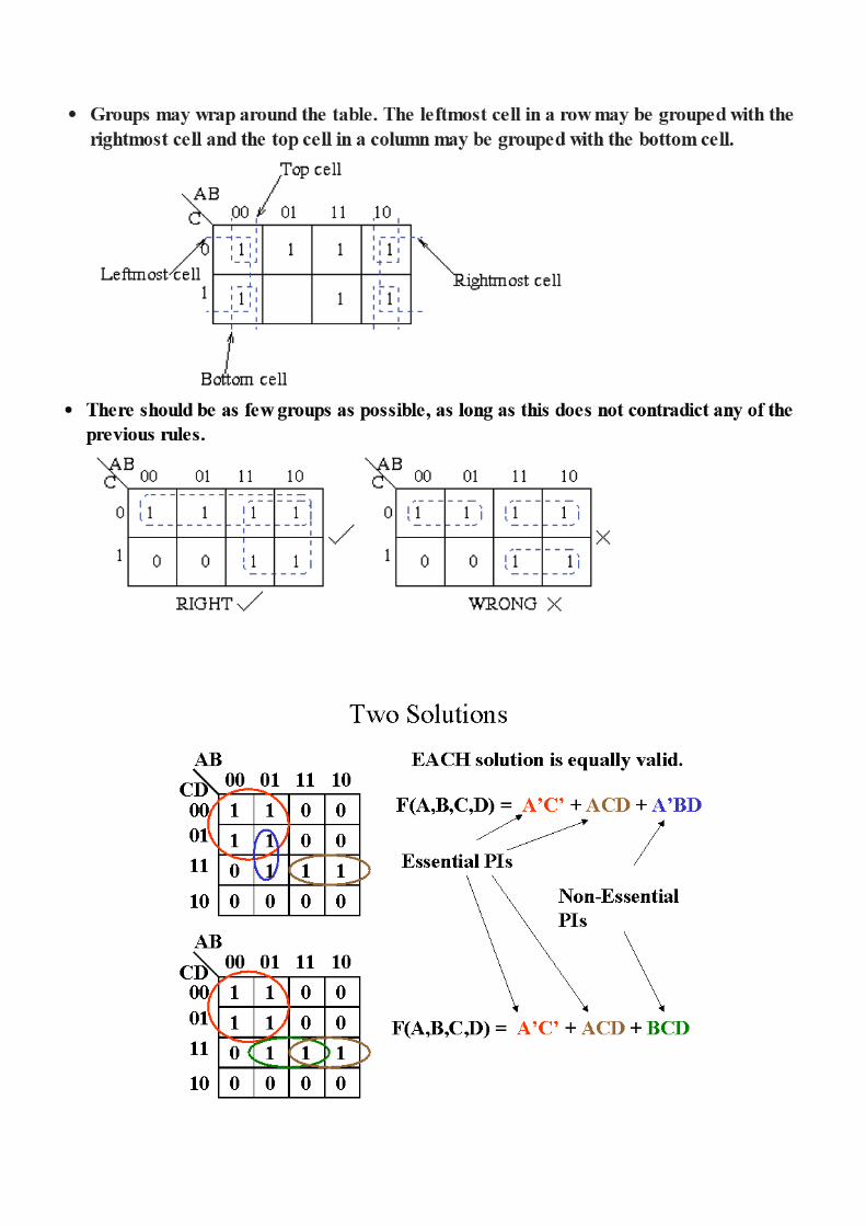
GROUPING:
1. Pair 2 adjacent 1’s eliminates 1 variable
2. Quad 4 adjacent 1’s eliminates 2 variables
3. Octet 8 adjacent 1’s eliminates 3 variable
Rules for Grouping :
1. No zeros are allowed.
2. No diagonal grouping is allowed.
3. Only power of 2 no. of cells in each group.
4. Group should be as large as possible.
5. Every 1 must be at least in a group.
6. Overlapping is allowed.
7. Wrap around is allowed.
8. Fewest number of groups allowed.


Don’t Care Condition:
• Minterms that may produce either 0 or 1 for the function.
• They are marked with an “x” in the K-map.
• This happens, for example, when we don’t input certain minterms to the Boolean function.
• These don’t-care conditions can be used to provide further simplification of the algebraic
expression.
Example:
F = A`B`C`+A`BC` + ABC`
D = A`B`C +A`BC + AB`C
F = A` + BC`
Implementation of SOP:
Example:
1. F(X,Y,Z) = XZ+Y’Z+X’YZ
The 1st level consists of AND gates, and
the 2nd
level consists of a single OR gate
•Also called 2-level Circuit
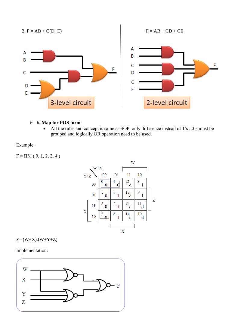
2. F = AB + C(D+E) F = AB + CD + CE
K-Map for POS form
All the rules and concept is same as SOP, only difference instead of 1’s , 0’s must be
grouped and logically OR operation need to be used.
Example:
F = ΠM ( 0, 1, 2, 3, 4 )
F= (W+X).(W+Y+Z)
Implementation:

Module 6: Combinational Logic Design
Syllabus : Introduction, Half and Full Adder, Half and Full Subtractor, Four Bit Binary Adder, One digit
BCD Adder, code conversion, Multiplexers and Demultiplexers, Decoders, 4-bit Magnitude Comparator IC
7485 and ALU IC74181.
Introduction:
Combinational circuit is circuit in which we combine the different gates in the circuit for example
encoder, decoder, multiplexer and demultiplexer.
Some of the characteristics of combinational circuits are as follows:
1. The output of combinational circuit at any instant of time, depends only on the levels present at
input terminals.
2. The combinational circuit do not use any memory.
3. The previous state of input does not have any effect on the present state of the circuit.
A combinational circuit can have a n-number of inputs and m number of outputs.
Block Diagram:
Half Adder
Half adder is a combinational logic circuit with two input and two output.
The half adder circuit is designed to add two sing le bit binary number A and B.
It is the basic building block for addition of two single bit numbers.
This circuit has two outputs carry and sum.
Block Diagram:
Truth Table:

K-Map:
Circuit Diagram:
Full Adder
Full adder is developed to overcome the drawback of Half Adder circuit.
It can add two one-bit numbers A and B, and carry c.
The full adder is a three input and two output combinational circuit.
Block Diagram:
Truth Table:

K-Map:
Circuit Diagram:
Half Subtractor
Half subtractor is a combination circuit with two inputs and two outputs (difference and
borrow).
It produces the difference between the two binary bits at the input and also produces a output
(Borrow) to indicate if a 1 has been borrowed.
In the subtraction (A-B), A is called as Minuend bit and B is called as Subtrahend bit.
Block Diagram:

Truth Table:
K-Map:
Circuit Diagram:
Four Bit Binary Adder
A binary adder is a digital circuit that produces the arithmetic sum of two binary
numbers.
It can be constructed with full adder connected in cascade, the output carry from each
full adder connected to the input carry of the next full adder in the chain.
Fig. below shows the interconnection of four full adder (FA) circuits to provide a 4-bit
binary ripple carry adder.
The augend bits of A and addend bits of B are designated by subscript numbers from
right to left , with subscript 0denoting the least significant bit.
The carries are connected in the chain through the full adders.
The input carry to the adder is C0 and it ripples through the full adder to the output
carry C4.
The S output generates the required sum bits.
The bits are added with full adders, starting from the position to form the sum bit and
carry.
The input carry C0 in the least significant position must be 0 . The value of Ci+1 in a
given significant position is the output carry of the full adder.

This value is transferred into the input carry of the full adder that adds the bits one
higher significant position to the left.
The sum bits are thus generated starting from the rightmost position and are available
for the correct sum bits to appears at the outputs.
The 4bit adder is a typical example of a standard component.
Block Diagram:
Block Diagram of IC 7483:
BCD Adder
A BCD adder is a digital circuit that produces the arithmetic sum of two BCD numbers,
which is also a BCD number.
Assume that two 4-bit BCD numbers A and B are being added. Then the 3 cases to be
considered namely;
Sum ≤ 9, Carry = 0 Sum ≤ 9, Carry = 1 Sum > 9, Carry = 0
Answer is Correct Add 6 to the sum to Add 6 to the sum to get
get correct answer correct answer
Truth Table:
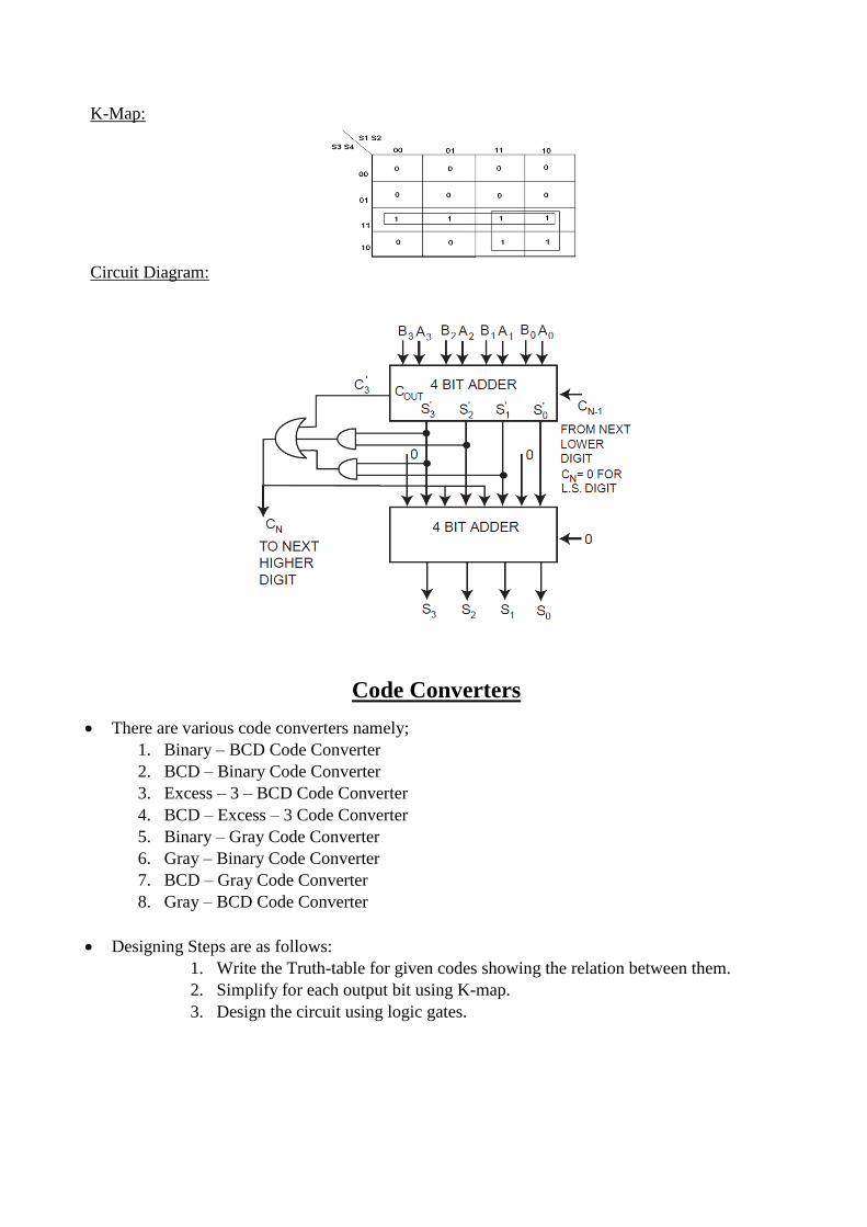
K-Map:
Circuit Diagram:
Code Converters
There are various code converters namely; 1. Binary – BCD Code Converter
2. BCD – Binary Code Converter
3. Excess – 3 – BCD Code Converter
4. BCD – Excess – 3 Code Converter
5. Binary – Gray Code Converter
6. Gray – Binary Code Converter
7. BCD – Gray Code Converter
8. Gray – BCD Code Converter
Designing Steps are as follows:
1. Write the Truth-table for given codes showing the relation between them.
2. Simplify for each output bit using K-map.
3. Design the circuit using logic gates.

Example:

K-MAP FOR G3:
Equation for G3= B3
K-MAP FOR G2:
Equation for G2= B3’ B2 + B3 B2’= B3 XOR B2
K-MAP FOR G1:
Equation for G1= B1’ B2 + B1 B2’= B1 XOR B2
K-MAP FOR G0:
Equation for G0= B1’ B0 + B1 B0’= B1 XOR B0
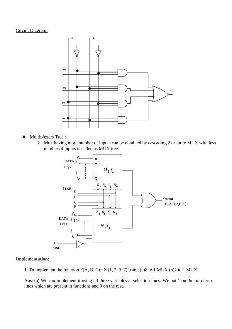
Multiplexers
Multiplexer is a special type of combinational circuit.
There are n-data inputs, one output and m select inputs with 2m
= n.
It is a digital circuit which selects one of the n data inputs and routes it to the output.
The selection of one of the n inputs is done by the selected inputs.
Depending on the digital code applied at the selected inputs, one out of n data sources is selected
and transmitted to the single output Y.
E is called the strobe or enable input which is useful for the cascading .
It is generally an active low terminal, which means it will perform the required operation when it is
low.

Block Diagram:
Multiplexers come in multiple variations
2 : 1 multiplexer
4 : 1 multiplexer
16 : 1 multiplexer
32 : 1 multiplexer
Example:
4:1 MUX
Block Diagram:
Truth - Table:
E S1 S0 Y
0 X X 0
1 0 0 D0
1 0 1 D1
1 1 0 D2
1 1 1 D3
4:1
MUX
4:1
MUX
D0 D0
D1 D1
D2 D2
D3 D3
E E S1 S1 S0 S0
OUTPUT OUTPUT
Circuit Diagram:
Multiplexers Tree : Mux having more number of inputs can be obtained by cascading 2 or more MUX with less
number of inputs is called as MUX tree.
Implementation:
1. To implement the function F(A, B, C)= Σ (1, 2, 5, 7) using (a)8 to 1 MUX (b)4 to 1 MUX
Ans: (a) We can implement it using all three variables at selection lines. We put 1 on the min term
lines which are present in functions and 0 on the rest.
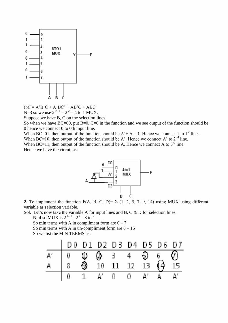
(b)F= A’B’C + A’BC’ + AB’C + ABC
N=3 so we use 2 N-1
= 2 2
= 4 to 1 MUX.
Suppose we have B, C on the selection lines.
So when we have BC=00, put B=0, C=0 in the function and we see output of the function should be
0 hence we connect 0 to 0th input line.
When BC=01, then output of the function should be A’+ A = 1. Hence we connect 1 to 1st line.
When BC=10, then output of the function should be A’. Hence we connect A’ to 2nd
line.
When BC=11, then output of the function should be A. Hence we connect A to 3rd
line.
Hence we have the circuit as:
2. To implement the function F(A, B, C, D)= Σ (1, 2, 5, 7, 9, 14) using MUX using different
variable as selection variable.
Sol. Let’s now take the variable A for input lines and B, C & D for selection lines.
N=4 so MUX is 2 N-1
= 23 = 8 to 1
So min terms with A in compliment form are 0 – 7
So min terms with A in un-compliment form are 8 – 15
So we list the MIN TERMS as:

And the circuit diagram is;
Applications of Multiplexer:
Multiplexer are used in various fields where multiple data need to be transmitted using a single line.
Following are some of the applications of multiplexers -
1. Communication system – Communication system is a set of systems that enable communication like
transmission system, relay and tributary station, and communication network. The efficiency of
communication system can be increased considerably using multiplexer. Multiplexer allow the
process of transmitting different type of data such as audio, video at the same time using a single
transmission line.
2. Telephone network – In telephone network, multiple audio signals are integrated on a single line for
transmission with the help of multiplexers. In this way, multiple audio signals can be isolated and
eventually, the desire audio signals reach the intended recipients.
3. Computer memory - Multiplexers are used to implement huge amount of memory into the computer,
at the same time reduces the number of copper lines required to connect the memory to other parts of
the computer circuit.
4. Transmission from the computer system of a satellite – Multiplexer can be used for the
transmission of data signals from the computer system of a satellite or spacecraft to the ground system
using the GPS (Global Positioning System) satellites.
De-Multiplexers
Demultiplexer means one to many.
A demultiplexer is a circuit with one input and many output.
By applying control signal, we can steer any input to the output.
Few types of demultiplexer are 1-to 2, 1-to-4, 1-to-8 and 1-to 16 demultiplexer.

Following figure illustrate the general idea of a demultiplexer with 1 input signal, m control
signals, and n output signals.
Example:
1:4 De-MUX
Block Diagram:
Truth Table:
E Data
Din S1 S0 Y0 Y1 Y2 Y3
0 X X X 0 0 0 0
1 Din 0 0 Din 0 0 0
1 Din 0 1 0 Din 0 0
1 Din 1 0 0 0 Din 0
1 Din 1 1 0 0 0 Din
Circuit Diagram:
1:4
De-MUX
1:4
De-MUX Din Din
Y0 Y0
Y1 Y1
Y2 Y2
Y3 Y3
E E S0 S0 S1 S1

De-Multiplexer Tree:
Example
Implementation:
1. Implement Full Subtractor using 1:8 De-Mux
Sol.
Truth-Table:
Equation:
D = f (A, B, Bin) = Σm (1, 2, 4, 7)
B0 = Σm (1, 2, 3, 7)
Logic Diagram:
A S2
B S1
Bin S0
1:8
De-Mux
1:8
De-Mux Din Din
Y0
Y1
Y2
Y3
Y4
Y5
Y6
Y7
Y0
Y1
Y2
Y3
Y4
Y5
Y6
Y7
E E
S2 S2 S1 S1 S0 S0
LOGIC 1 LOGIC 1
D D
Bo Bo

Applications of Demultiplexer:
1. Demultiplexer is used to connect a single source to multiple destinations. The main application area
of demultiplexer is communication system where multiplexer are used. Most of the communication
system are bidirectional i.e. they function in both ways (transmitting and receiving signals). Hence,
for most of the applications, the multiplexer and demultiplexer work in sync. Demultiplexer are also
used for reconstruction of parallel data and ALU circuits.
2. Communication System - Communication system use multiplexer to carry multiple data like audio,
video and other form of data using a single line for transmission. This process make the transmission
easier. The demultiplexer receive the output signals of the multiplexer and converts them back to the
original form of the data at the receiving end. The multiplexer and demultiplexer work together to
carry out the process of transmission and reception of data in communication system.
3. ALU (Arithmetic Logic Unit) – In an ALU circuit, the output of ALU can be stored in multiple
registers or storage units with the help of demultiplexer. The output of ALU is fed as the data input to
the demultiplexer. Each output of demultiplexer is connected to multiple register which can be stored
in the registers.
4. Serial to parallel converter - A serial to parallel converter is used for reconstructing parallel data
from incoming serial data stream. In this technique, serial data from the incoming serial data stream
is given as data input to the demultiplexer at the regular intervals. A counter is attach to the control
input of the demultiplexer. This counter directs the data signal to the output of the demultiplexer
where these data signals are stored. When all data signals have been stored, the output of the
demultiplexer can be retrieved and read out in parallel.

Decoders and Encoders Lesson Objectives In this lesson, we will learn about o Decoders o Expansion of decoders o Combinational circuit implementation with decoders o Some examples of decoders o Encoders o Major limitations of encoders o Priority encoders o Some examples of ecnoders
Decoders As its name indicates, a decoder is a circuit component that decodes an input code. Given a binary code of n-bits, a decoder will tell which code is this out of the 2n possible codes (See Figure 1(a)).
n Inputsn-to-2n
Decoder
01
2n-1
Figure 1(a): A typical decoder Thus, a decoder has n- inputs and 2n outputs. Each of the 2n outputs corresponds to one of the possible 2n input combinations.
n Inputsn-to-2n
Decoder 2n Outputs
Enable Figure 1(b): A typical decoder
Figure 1(b) shows the block diagram of a typical decoder, which has n input lines, and m output lines, where m is equal to 2n. The decoder is called n-to-m decoder. Apart from this, there is also a single line connected to the decoder called enable line. The operations of the enable line will be discussed in the flowing text.

o In general, output i equals 1 if and only if the input binary code has a value of i. o Thus, each output line equals 1 at only one input combination but is equal to 0 at
all other combinations. o In other words, each decoder output corresponds to a minterm of the n input
variables. o Thus, the decoder generates all of the 2n minterms of n input variables.
Example: 2-to-4 decoders Let us discuss the operation and combinational circuit design of a decoder by taking the specific example of a 2-to-4 decoder. It contains two inputs denoted by A1 and A0 and four outputs denoted by D0, D1, D2, and D3 as shown in figure 2. Also note that A1 is the MSB while A0 is the LSB.
A0 2-to-4DecoderA1
D0 = A1A0
D1 = A1A0
D2 = A1A0
D3 = A1A0
Figure 2: A 2-to-4 decoder without enable
Decimal # Input Output
A1 A0 D0 D1 D2 D3 0 0 0 1 0 0 0 1 0 1 0 1 0 0 2 1 0 0 0 1 0 3 1 1 0 0 0 1
Table 1: Truth table for 2-to-4 decoder
As we see in the truth table (table 1), for each input combination, one output line is activated, that is, the output line corresponding to the input combination becomes 1, while other lines remain inactive. For example, an input of 00 at the input will activate line D0. 01 at the input will activate line D1, and so on.

o Notice that, each output of the decoder is actually a minterm resulting from a certain combination of the inputs, that is o D0 =A1 A0, ( minterm m0) which corresponds to input 00 o D1 =A1 A0, ( minterm m1) which corresponds to input 01 o D2 =A1 A0, ( minterm m2) which corresponds to input 10 o D3 =A1 A0, ( minterm m3) which corresponds to input 11
o This is depicted in Figures 2 where we see that each input combination will
inovke the corresponding output, where each output is minterm corresponding to the input combination.
A1A0
D0 = A1A0
D1 = A1A0
D2 = A1A0
D3 = A1A0
Figure 3: Implementation 2-to-4 decoder The circuit is implemented with AND gates, as shown in figure 3. In this circuit we see that the logic equation for D0 is A1
/ A0/. D0 is A1
/ A0, and so on. These are in fact the minterms being implemented. Thus, each output of the decoder generates a minterm corresponding to the input combination. The “enable” input in decoders Generally, decoders have the “enable” input .The enable input perroms no logical operation, but is only responsible for making the decoder ACTIVE or INACTIVE. o If the enable “E”
o is zero, then all outputs are zero regardless of the input values. o is one, then the decoder performs its normal operation.
For example, consider the 2-to-4 decoder with the enable input (Figure 4). The enable input is only responsible for making the decoder active or inactive. If Enable E is zero, then all outputs of the decoder will be zeros, regardless of the values of A1 and A0. However, if E is 1, then the decoder will perform its normal operation, as is shown in the

truth table (table 2). In this table we see that as long as E is zero, the outputs D0 to D3 will remain zero, no matter whatever value you provide at the inputs A1 A0, depicted by two don’t cares. When E becomes 1, then we see the same behavior as we saw in the case of 2-to-4 decoder discussed earlier.
D1
D2
D3
A1A0
D0
E
Figure 4: Implementation 2-to-4 decoder with enable
Decimal value
Enable Inputs Outputs
E A1 A0 D0 D1 D2 D3 0 X X 0 0 0 0 0 1 0 0 1 0 0 0 1 1 0 1 0 1 0 0 2 1 1 0 0 0 1 0 3 1 1 1 0 0 0 1
Table 2: Truth table of 2-to-4 decoder with enable
Example: 3-to-8 decoders In a three to eight decoder, there are three inputs and eight outputs, as shown in figure 5. A0 is the least significant variable, while A2 is the most significant variable. The three inputs are decoded into eight outputs. That is, binary values at the input form a combination, and based on this combination, the corresponding output line is activated.

A0 3-to-8Decoder
Enable
A1
A2
D0 = A2A1A0
D1 = A2A1A0
D2 = A2A1A0
D3 = A2A1A0
D4 = A2A1A0
D5 = A2A1A0D6 = A2A1A0D7 = A2A1A0
Figure 5: A 3-to-8 decoder with enable
Each output represents one minterm . o For example, for input combination A2A1A0 = 001, output line D1 equals 1 while all
other output lines equal 0’s o It should be noted that at any given instance of time, one and only one output line
can be activated. It is also obvious from the fact that only one combination is possible at the input at a time, so the corresponding output line is activated.
Dec. Inputs Outputs Code A2 A1 A0 D0 D1 D2 D3 D4 D5 D6 D7
0 0 0 0 1 0 0 0 0 0 0 0 1 0 0 1 0 1 0 0 0 0 0 0 2 0 1 0 0 0 1 0 0 0 0 0 3 0 1 1 0 0 0 1 0 0 0 0 4 1 0 0 0 0 0 0 1 0 0 0 5 1 0 1 0 0 0 0 0 1 0 0 6 1 1 0 0 0 0 0 0 0 1 0 7 1 1 1 0 0 0 0 0 0 0 1
Table 3: Truth table of 3-to-8 decoder
Since each input combination represents one minterm, the truth table (table 3) contains eight output functions, from D0 to D7 seven, where each function represents one and only one minterm. Thus function D0 is A2
/ A1/ A0
/. Similarly function D7 is A2A1A0. The corresponding circuit is given in Figure 6. In this figure, the three inverters provide complement of the inputs, and each one of the AND gates generates one of the minterms. It is also possible to add an Enable input to this decoder.
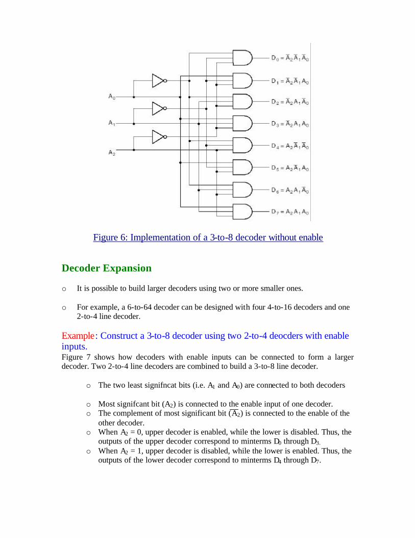
Figure 6: Implementation of a 3-to-8 decoder without enable Decoder Expansion o It is possible to build larger decoders using two or more smaller ones.
o For example, a 6-to-64 decoder can be designed with four 4-to-16 decoders and one
2-to-4 line decoder. Example: Construct a 3-to-8 decoder using two 2-to-4 deocders with enable inputs. Figure 7 shows how decoders with enable inputs can be connected to form a larger decoder. Two 2-to-4 line decoders are combined to build a 3-to-8 line decoder.
o The two least signifncat bits (i.e. A1 and A0) are connected to both decoders
o Most signifcant bit (A2) is connected to the enable input of one decoder. o The complement of most significant bit (A2) is connected to the enable of the
other decoder. o When A2 = 0, upper decoder is enabled, while the lower is disabled. Thus, the
outputs of the upper decoder correspond to minterms D0 through D3. o When A2 = 1, upper decoder is disabled, while the lower is enabled. Thus, the
outputs of the lower decoder correspond to minterms D4 through D7.
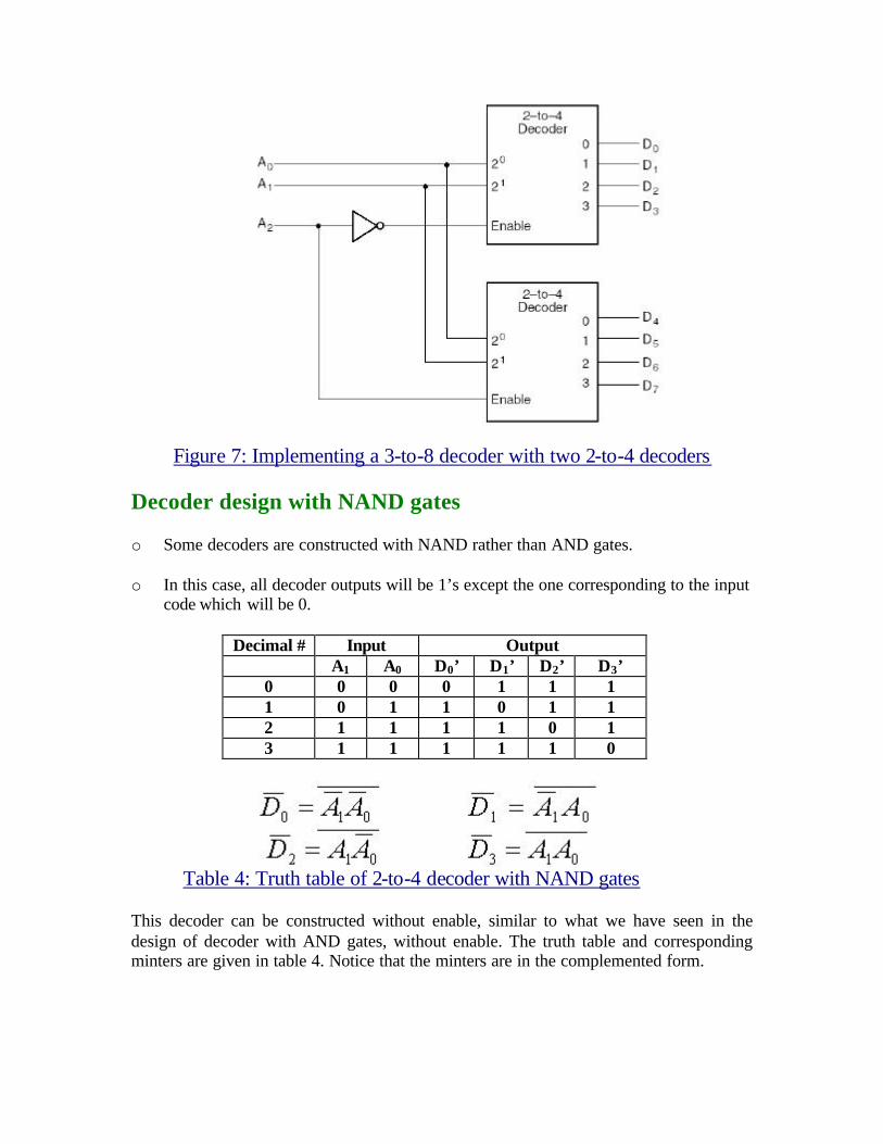
Figure 7: Implementing a 3-to-8 decoder with two 2-to-4 decoders Decoder design with NAND gates o Some decoders are constructed with NAND rather than AND gates. o In this case, all decoder outputs will be 1’s except the one corresponding to the input
code which will be 0.
Decimal # Input Output A1 A0 D0’ D1’ D2’ D3’ 0 0 0 0 1 1 1 1 0 1 1 0 1 1 2 1 1 1 1 0 1 3 1 1 1 1 1 0
Table 4: Truth table of 2-to-4 decoder with NAND gates
This decoder can be constructed without enable, similar to what we have seen in the design of decoder with AND gates, without enable. The truth table and corresponding minters are given in table 4. Notice that the minters are in the complemented form.

Figure 8: A 2-to-4 decoder with Enable constructed with NAND gates.
Decimal value
Enable Inputs Outputs
E’ A1 A0 D0’ D1’ D2’ D3’ 1 X X 1 1 1 1 0 0 0 0 0 1 1 1 1 0 0 1 1 0 1 1 2 0 1 1 1 1 0 1 3 0 1 1 1 1 1 0
Table 5: Truth table of 2-to-4 decoder with Enable using NAND gates A 2-to-4 line decoder with an enable input constructed with NAND gates is shown in figure 8. The circuit operates with complemented outputs and enable input E’ is also complemented to match the outputs of the NAND gate decoder. The decoder is enabled when E’ is equal to zero. As indicated by the truth table, only one output can be equal to zero at any given time, all other outputs being equal to one. The output with the value of zero represents the minterm selected by inputs A1 and A0. The circuit is disabled when E’ is equal to one, regardless of the values of the other two inputs. When the circuit is disabled, none of the outputs are equal to zero, and none of the minterms are selected. The corresponding logic equations are also given in table 5. Combinational circuit implementation using decoder o As known, a decoder provides the 2n minterms of n input variables o Since any boolean functions can be expressed as a sum of minterms, one can use a
decoder to implement any function of n variables. o In this case, the decoder is used to generate the 2n minterms and an additional OR
gate is used to generate the sum of the required minterms. o In this way, any combinational circuit with n inputs and m outputs can be

implemented using an n-to-2n decoder in addition to m OR gates. ? Remember, that o The function need not be simplified since the decoder implements a function using
the minterms, not product terms. o Any number of output functions can be implemented using a single decoder,
provided that all those outputs are functions of the same input variables. Example: Decoder Implementation of a Full Adder Let us look at the truth table (table 6) for the given problem. We have two outputs, called S, which stands for sum, and C, which stands for carry. Both sum and carry are functions of X, Y, and Z.
Decimal value
Input Output
X Y Z S C 0 0 0 0 0 0
1 0 0 1 1 0
2 0 1 0 1 0
3 0 1 1 0 1
4 1 0 0 1 0
5 1 0 1 0 1
6 1 1 0 0 1
7 1 1 1 1 1
Table 6: Truth table of the Full Adder
o The output functions S & C can be expressed in sum-of-minterms forms as follows:
o S (X,Y,Z) = m (1,2,4,7) o C (X,Y,Z) = m (3,5,6,7)
Looking at the truth table and the functions in sum of minterms form, we observe that there are three inputs, X, Y, and Z that correspond to eight minterms. This implies that a 3-to-8 decoder is needed to implement this function. This implementation is given in Figure 9, where the sum S is implemented by taking minterms 1, 2, 4, and 7 and the OR gates forms the logical sum of minterm for S. Similarly, carry C is implemented by taking logical sum of minterms 3, 5, 6, and 7 from the same decoder.
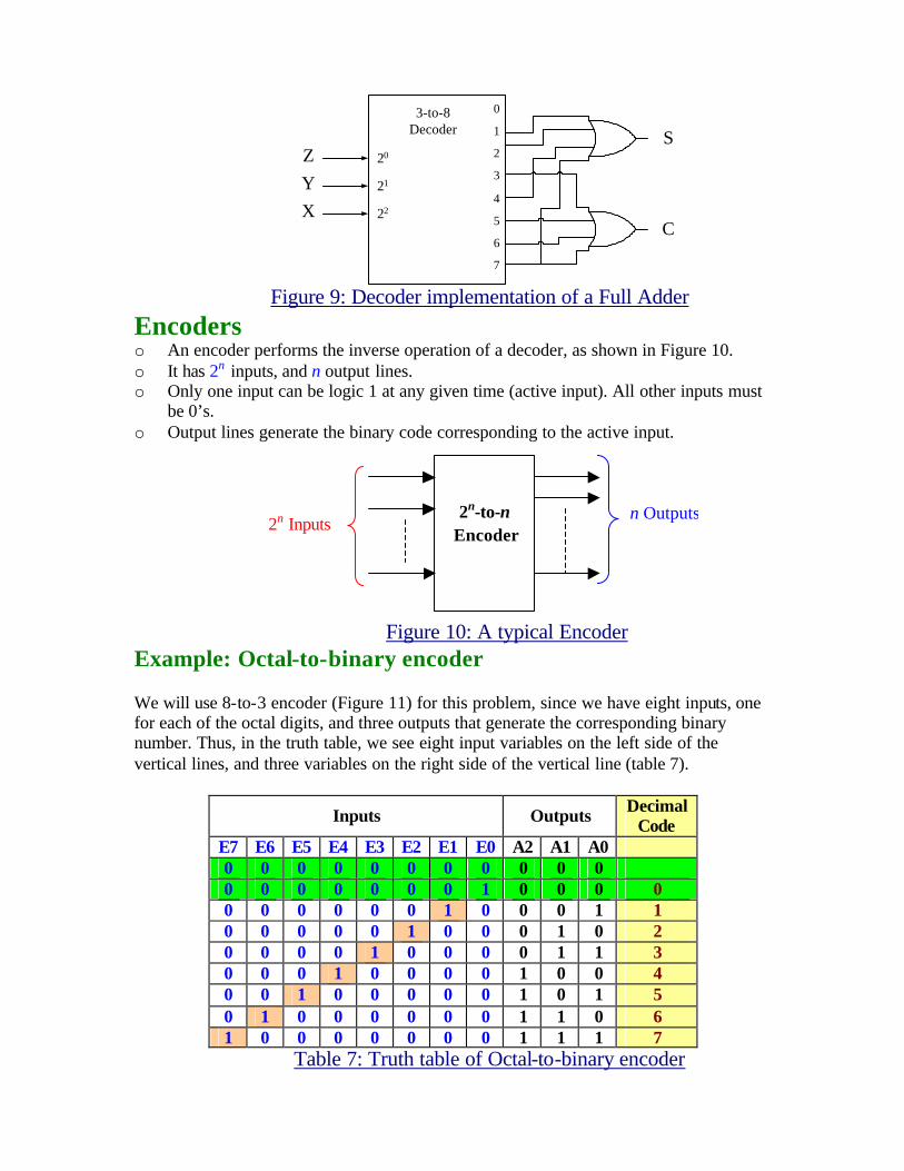
ZYX
3-to-8Decoder
20
21
22
0
7
6
5
4
3
2
1 S
C
Figure 9: Decoder implementation of a Full Adder
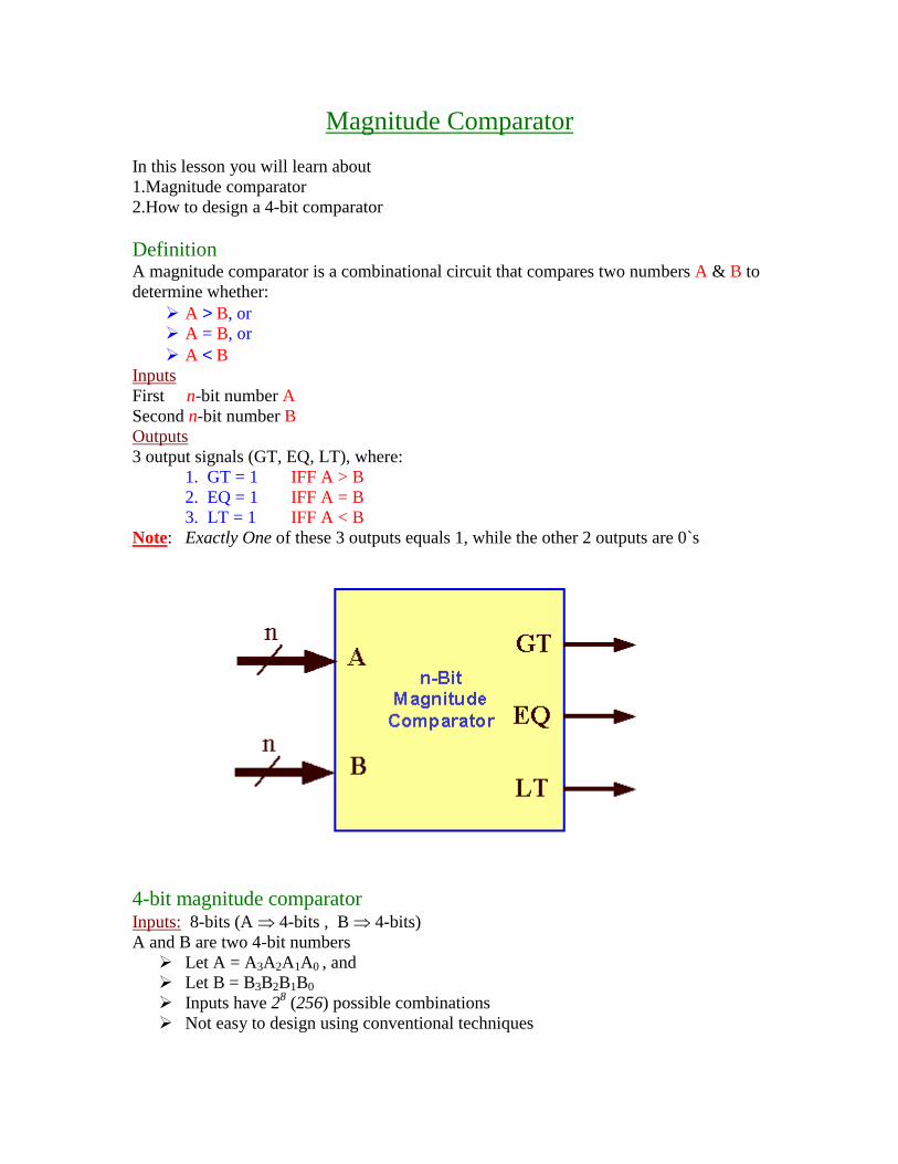
Encoders o An encoder performs the inverse operation of a decoder, as shown in Figure 10. o It has 2n inputs, and n output lines. o Only one input can be logic 1 at any given time (active input). All other inputs must
be 0’s. o Output lines generate the binary code corresponding to the active input.
Figure 10: A typical Encoder
Example: Octal-to-binary encoder We will use 8-to-3 encoder (Figure 11) for this problem, since we have eight inputs, one for each of the octal digits, and three outputs that generate the corresponding binary number. Thus, in the truth table, we see eight input variables on the left side of the vertical lines, and three variables on the right side of the vertical line (table 7).
Inputs Outputs Decimal Code
E7 E6 E5 E4 E3 E2 E1 E0 A2 A1 A0 0 0 0 0 0 0 0 0 0 0 0 0 0 0 0 0 0 0 1 0 0 0 0 0 0 0 0 0 0 1 0 0 0 1 1 0 0 0 0 0 1 0 0 0 1 0 2 0 0 0 0 1 0 0 0 0 1 1 3 0 0 0 1 0 0 0 0 1 0 0 4 0 0 1 0 0 0 0 0 1 0 1 5 0 1 0 0 0 0 0 0 1 1 0 6 1 0 0 0 0 0 0 0 1 1 1 7
Table 7: Truth table of Octal-to-binary encoder
2n-to-n Encoder
2n Inputs n Outputs

Figure 11: Octal-to-binary encoder o Note that not all input combinations are valid. o Valid combinations are those which have exactly one input equal to logic 1 while all
other inputs are logic 0’s. o Since, the number of inputs = 8, K-maps cannot be used to derive the output Boolean
expressions. o The encoder implementation, however, can be directly derived from the truth table
o Since A0 = 1 if the input octal digit is 1 or 3 or 5 or 7, then we can write: A0 = E1 + E3 + E5+ E7
o Likewise, A1 = E2 + E3 + E6+ E7, and similarly o A2 = E4 + E5 + E6+ E7
o Thus, the encoder can be implemented using three 4- input OR gates. Major Limitation of Encoders o Exactly one input must be active at any given time. o If the number of active inputs is less than one or more than one, the output will be
incorrect. o For example, if E3 = E6 = 1, the output of the encoder A2A1A0 = 111, which implies
incorrect output.
Two Problems to Resolve. 1. If two or more inputs are active at the same time, what should the output be? 2. An output of all 0's is generated in 2 cases:
o when all inputs are 0 o when E0 is equal to 1.
How can this ambiguity be resolved? Solution To Problem 1: o Use a Priority Encoder which produces the output corresponding to the input with
higher priority. o Inputs are assigned priorities according to their subscript value; e.g. higher subscript
inputs are assigned higher priority. o In the previous example, if E3 = E6 = 1, the output corresponding to E6 will be
produced (A2A1A0 = 110) since E6 has higher priority than E3.
3 Outputs
A0 A1 A2
8-to-3 Encoder
8 Inputs
E0 E1 E2 E3 E4 E5 E6 E7

Solution To Problem 2: o Provide one more output signal V to indicate validity of input data. o V = 0 if none of the inputs equals 1, otherwise it is 1 Example: 4-to-2 Priority Encoders o Sixteen input combinations o Three output variables A1, A0, and V o V is needed to take care of situation when all inputs are equal to zero.
Table 8: Truth table of 4-to-2 Priority Encoder In the truth table (table 8), we have sixteen input combinations. In the output, we have three variables. The variable V is needed to take care of the situation where all inputs are zero. In that case V is kept at zero, regardless of the values of A1 and A0. This combination is highlighted green. In all other cases, V is kept at 1, because at least one of the inputs is one. When E0 is 1, the output combination of A1 and A0 is 00. This combination is highlighted blue. Then we have two combinations highlighted yellow. In both these combinations, A1 and A0 are 01. This is because in both these combinations E1 is 1, regardless of the value of E0, and since E1 has higher subscript, the corresponding output value is 01. This is followed by four input combinations in pink. In these four combinations, the output A1A0 is 10, since E2 is 1 in all these combinations, and E2 has the highest
Inputs
E3 E2 E1 E0 A1 A0 V 0 0 0 0 X X 0 0 0 0 1 0 0 1 0 0 1 0 0 1 1 0 0 1 1 0 1 1 0 1 0 0 1 0 1 0 1 0 1 1 0 1 0 1 1 0 1 0 1 0 1 1 1 1 0 1 1 0 0 0 1 1 1 1 0 0 1 1 1 1 1 0 1 0 1 1 1 1 0 1 1 1 1 1 1 1 0 0 1 1 1 1 1 0 1 1 1 1 1 1 1 0 1 1 1 1 1 1 1 1 1 1
Outputs
Invalid Input

precedence compared to E0 and E1. Although E0 and E1 are also having a value of one in this set of four combinations, but they do not have the priority. Finally we have the last eight input combinations, whose output is 11. This is because E3 is the highest priority input, and it is equal to 1. Though the other inputs with smaller subscripts, namely, E2, E1, and E0 are also having values of one in some combinations, but they do not have the priority. The truth table can be rewritten in a more compact form using don’t care conditions for inputs as shown below in table 9.
Table 9: Truth table of 4-to-2 priority encoder (compact form) o With 4 Input variables, the truth table must have 16 rows, with each row
representing an input combination. o With don’t care input conditions, the number of rows can be reduced since rows with
don’t care inputs will actually represent more than one input combination. o Thus, for example, row # 3 represents 2 combinations since it represents the input
conditions E3E2E1E0=0010 and 0011. o Likewise, row # 4 represents 4 combinations since it represents the input conditions
E3E2E1E0=0100, 0101, 0110 and 0111. o Similarly, row # 5 represents 8 combinations. o Thus, the total number of input combinations represented by the 5-row truth table =
1+ 1+ 2+ 4 + 8= 16 input combinations. Boolean Expressions for V, A1 and A0 and the circuit: See next page:
E3 E2 E1 E0 A1 A0 V 1 0 0 0 0 X X 0 2 0 0 0 1 0 0 1 3 0 0 1 X 0 1 1 4 0 1 X X 1 0 1 5 1 X X X 1 1 1
Inputs Outputs

Figure 12: Equations and circuit for 4-to-2 priority encoder
Magnitude Comparator In this lesson you will learn about 1.Magnitude comparator 2.How to design a 4-bit comparator Definition A magnitude comparator is a combinational circuit that compares two numbers A & B to determine whether: � A > B, or � A = B, or � A < B
Inputs First n-bit number A Second n-bit number B Outputs 3 output signals (GT, EQ, LT), where: 1. GT = 1 IFF A > B 2. EQ = 1 IFF A = B 3. LT = 1 IFF A < B Note: Exactly One of these 3 outputs equals 1, while the other 2 outputs are 0`s
4-bit magnitude comparator Inputs: 8-bits (A ⇒ 4-bits , B ⇒ 4-bits) A and B are two 4-bit numbers � Let A = A3A2A1A0 , and � Let B = B3B2B1B0 � Inputs have 28 (256) possible combinations � Not easy to design using conventional techniques

The circuit possesses certain amount of regularity ⇒ can be designed algorithmically. Design of the EQ output (A = B) in 4-bit magnitude comparator Define Xi = (Ai Bi)+ (Ai
/ Bi /)
Thus Xi = 1 IFF Ai = Bi ∀ i =0, 1, 2 and 3
Xi = 0 IFF Ai ≠ Bi Condition for A= B EQ=1 (i.e., A=B) IFF
1. A3=B3 → (X3 = 1), and 2. A2=B2 → (X2 = 1), and 3. A1=B1 → (X1 = 1), and 4. A0=B0 → (X0 = 1).
Thus, EQ=1 IFF X3 X2 X1 X0 = 1. In other words, EQ = X3 X2 X1 X0 Design of the GT output (A > B) 4-bit magnitude comparator If A3 > B3, then A > B (GT=1) irrespective of the relative values of the other bits of A & B. Consider, for example, A = 1000 and B = 0111 where A > B. This can be stated as GT=1 if A3 B3
/ =1 If A3 = B3 (X3 = 1), we compare the next significant pair of bits (A2 & B2). If A2 > B2 then A > B (GT=1) irrespective of the relative values of the other bits of A & B. Consider, for example, A = 0100 and B = 0011 where A > B. This can be stated as GT=1 if X3A2 B2
/ =1 If A3 = B3 (X3 = 1) and A2 = B2 (X2 = 1), we compare the next significant pair of bits (A1 & B1).

If A1 > B1 then A > B (GT=1) irrespective of the relative values of the remaining bits A0 & B0. Consider, for example, A = 0010 and B = 0001 where A > B This can be stated as GT=1 if X3 X2A1 B1
/ =1 If A3 = B3 (X3 = 1) and A2 = B2 (X2 = 1) and A1 = B1 (X1 = 1), we compare the next pair of bits (A0 & B0). If A0 > B0 then A > B (GT=1). This can be stated as GT=1 if X3X2X1A0B0
/=1 To summarize, GT =1 (A > B) IFF:
1. A3 B3/ =1, or
2. X3A2 B2/ =1, or
3. X3 X2A1 B1/ = 1, or
4. X3X2X1A0B0/ =1
In other words, GT = A3 B3/ + X3A2 B2
/ + X3 X2A1 B1/ + X3X2X1A0B0
/
Design of the LT output (A < B) 4-bit magnitude comparator In the same manner as above, we can derive the expression of the LT (A < B) output LT = B3 A3
/ + X3B2 A2/ + X3 X2B1 A1
/ + X3X2X1B0A0/
The gate implementation of the three output variables (EQ, GT & LT) is shown in the figure below.
A3
B3
A2
B2
A0
B0
A1
B1
A < B
A > B
A = B

Modification to the Design The hardware in the comparator can be reduced by implementing only two outputs, and the third output can be obtained using these two outputs. For example, if we have the LT and GT outputs, then the EQ output can be obtained by using only a NOR gate, as shown in the figure below.
Thus, when both the GT and LT outputs are zeros, then the 3rd one (i.e. EQ) is a ‘1’

S0 – S3
ARITHMETIC LOGIC UNIT (IC 74181)
An arithmetic logic unit, or ALU is a combinational network that implements a function of its inputs
based on either logic or arithmetic operations.
ALUs are at the heart of all computers as well as most digital hardware systems.
IC 74181 is a 4-bit ALU.
Features: 1. Provides 16 arithmetic operations : addition, subtraction, comparison, double, & +12 other
arithmetic operations.
2. Provides all 16 logic operations of 2 variables namely; EX-OR, Compare, AND, NAND, OR,
NOR, & +10 other logic operations.
3. Full lookahead for high speed arithmetic operation on long words.
Block Diagram :
As shown in above diagram, IC 74S181 has following:
1. Two 4-bit operands - A0 – A3 and B0 – B3
2. Its mode select input selects one of the two modes - M : arithmetic or logical &
3. 4 function select inputs - S0 – S3 select a particular function from the selected mode.
Mode
Control
ALU
A0 – A3
B0 – B3
Cn
Carry Input
F0 – F3
Select
Inputs
M
Cn+4 Carry output
A=B Equality output
G Generate output
P Propagate output

IC 74181 Connection Diagram:
Pin detail & Function table:-

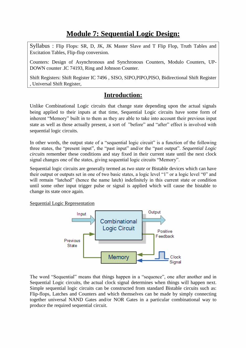
Module 7: Sequential Logic Design:
Syllabus : Flip Flops: SR, D, JK, JK Master Slave and T Flip Flop, Truth Tables and
Excitation Tables, Flip-flop conversion.
Counters: Design of Asynchronous and Synchronous Counters, Modulo Counters, UP-
DOWN counter .IC 74193, Ring and Johnson Counter.
Shift Registers: Shift Register IC 7496 , SISO, SIPO,PIPO,PISO, Bidirectional Shift Register
, Universal Shift Register,
Introduction:
Unlike Combinational Logic circuits that change state depending upon the actual signals
being applied to their inputs at that time, Sequential Logic circuits have some form of
inherent “Memory” built in to them as they are able to take into account their previous input
state as well as those actually present, a sort of ”before” and “after” effect is involved with
sequential logic circuits.
In other words, the output state of a “sequential logic circuit” is a function of the following
three states, the “present input”, the “past input” and/or the “past output”. Sequential Logic
circuits remember these conditions and stay fixed in their current state until the next clock
signal changes one of the states, giving sequential logic circuits “Memory”.
Sequential logic circuits are generally termed as two state or Bistable devices which can have
their output or outputs set in one of two basic states, a logic level “1” or a logic level “0” and
will remain “latched” (hence the name latch) indefinitely in this current state or condition
until some other input trigger pulse or signal is applied which will cause the bistable to
change its state once again.
Sequential Logic Representation
The word “Sequential” means that things happen in a “sequence”, one after another and in
Sequential Logic circuits, the actual clock signal determines when things will happen next.
Simple sequential logic circuits can be constructed from standard Bistable circuits such as:
Flip-flops, Latches and Counters and which themselves can be made by simply connecting
together universal NAND Gates and/or NOR Gates in a particular combinational way to
produce the required sequential circuit.
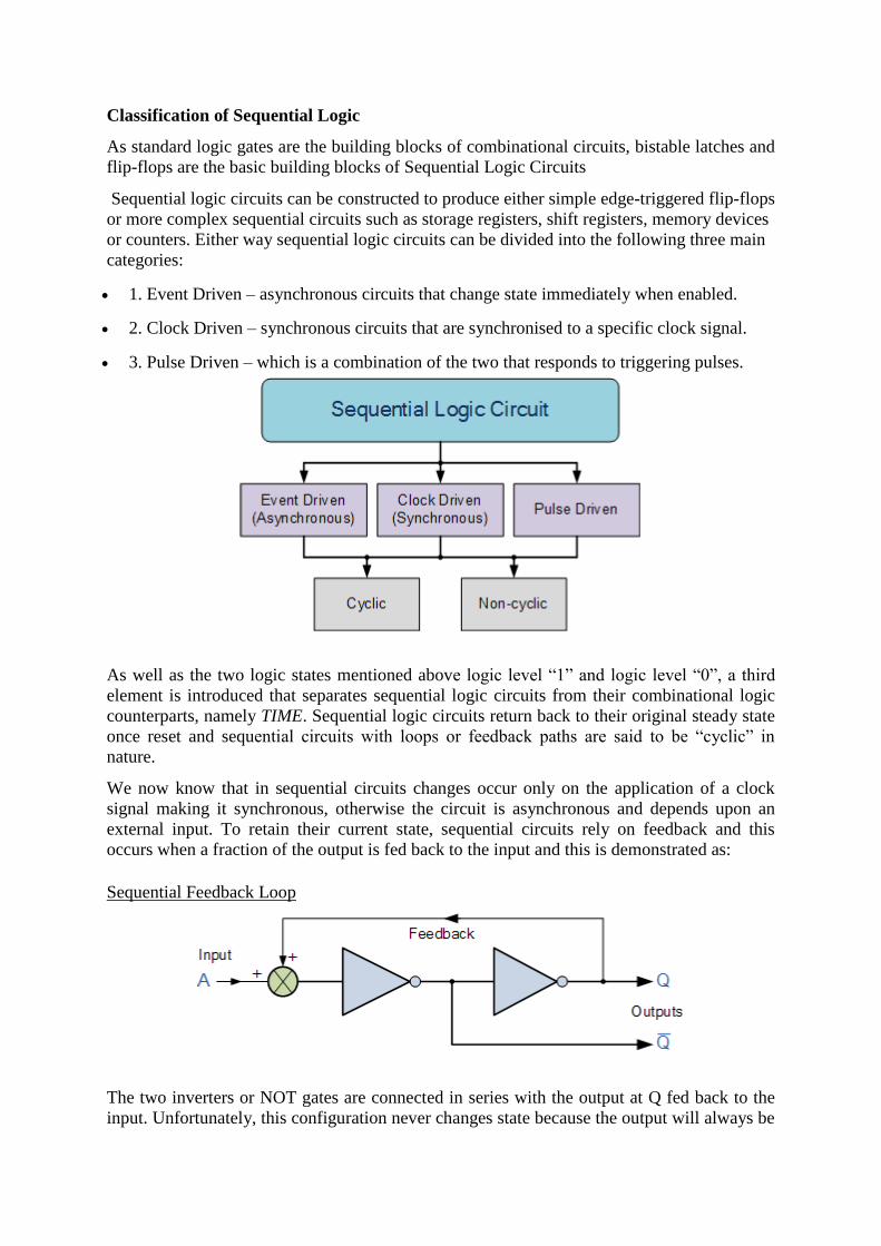
Classification of Sequential Logic
As standard logic gates are the building blocks of combinational circuits, bistable latches and
flip-flops are the basic building blocks of Sequential Logic Circuits
Sequential logic circuits can be constructed to produce either simple edge-triggered flip-flops
or more complex sequential circuits such as storage registers, shift registers, memory devices
or counters. Either way sequential logic circuits can be divided into the following three main
categories:
1. Event Driven – asynchronous circuits that change state immediately when enabled.
2. Clock Driven – synchronous circuits that are synchronised to a specific clock signal.
3. Pulse Driven – which is a combination of the two that responds to triggering pulses.
As well as the two logic states mentioned above logic level “1” and logic level “0”, a third
element is introduced that separates sequential logic circuits from their combinational logic
counterparts, namely TIME. Sequential logic circuits return back to their original steady state
once reset and sequential circuits with loops or feedback paths are said to be “cyclic” in
nature.
We now know that in sequential circuits changes occur only on the application of a clock
signal making it synchronous, otherwise the circuit is asynchronous and depends upon an
external input. To retain their current state, sequential circuits rely on feedback and this
occurs when a fraction of the output is fed back to the input and this is demonstrated as:
Sequential Feedback Loop
The two inverters or NOT gates are connected in series with the output at Q fed back to the
input. Unfortunately, this configuration never changes state because the output will always be

the same, either a “1” or a “0”, it is permanently set. However, we can see how feedback
works by examining the most basic sequential logic components, called the SR flip-flop.
Flip - Flops
1. SR Flip-Flop
The SR flip-flop, also known as a SR Latch, can be considered as one of the most basic
sequential logic circuit possible. This simple flip-flop is basically a one-bit memory bistable
device that has two inputs, one which will “SET” the device (meaning the output = “1”), and
is labelled S and another which will “RESET” the device (meaning the output = “0”), labelled
R.
Then the SR description stands for “Set-Reset”. The reset input resets the flip-flop back to its
original state with an output Q that will be either at a logic level “1” or logic “0” depending
upon this set/reset condition.
A basic NAND gate SR flip-flop circuit provides feedback from both of its outputs back to its
opposing inputs and is commonly used in memory circuits to store a single data bit. Then the
SR flip-flop actually has three inputs, Set, Reset and its current output Q relating to it’s
current state or history. The term “Flip-flop” relates to the actual operation of the device, as it
can be “flipped” into one logic Set state or “flopped” back into the opposing logic Reset state.
The NAND Gate SR Flip-Flop
The simplest way to make any basic single bit set-reset SR flip-flop is to connect together a
pair of cross-coupled 2-input NAND gates as shown, to form a Set-Reset Bistable also known
as an active LOW SR NAND Gate Latch, so that there is feedback from each output to one of
the other NAND gate inputs. This device consists of two inputs, one called the Set, S and the
other called the Reset, R with two corresponding outputs Q and its inverse or complement Q
(not-Q) as shown below.
The Basic SR Flip-flop
The Set State
Consider the circuit shown above. If the input R is at logic level “0” (R = 0) and input S is at
logic level “1” (S = 1), the NAND gate Y has at least one of its inputs at logic “0” therefore,
its output Q must be at a logic level “1” (NAND Gate principles). Output Q is also fed back

to input “A” and so both inputs to NAND gate X are at logic level “1”, and therefore its
output Q must be at logic level “0”.
Again NAND gate principals. If the reset input R changes state, and goes HIGH to logic “1”
with S remaining HIGH also at logic level “1”, NAND gate Y inputs are now R = “1” and B =
“0”. Since one of its inputs is still at logic level “0” the output at Q still remains HIGH at
logic level “1” and there is no change of state. Therefore, the flip-flop circuit is said to be
“Latched” or “Set” with Q = “1” and Q = “0”.
Reset State
In this second stable state, Q is at logic level “0”, (not Q = “0”) its inverse output at Q is at
logic level “1”, (Q = “1”), and is given by R = “1” and S = “0”. As gate X has one of its
inputs at logic “0” its output Q must equal logic level “1” (again NAND gate principles).
Output Q is fed back to input “B”, so both inputs to NAND gate Y are at logic “1”, therefore,
Q = “0”.
If the set input, S now changes state to logic “1” with input R remaining at logic “1”, output
Q still remains LOW at logic level “0” and there is no change of state. Therefore, the flip-flop
circuits “Reset” state has also been latched and we can define this “set/reset” action in the
following truth table.
Truth Table for this Set-Reset Function
State S R Q Q Description
Set 1 0 0 1 Set Q » 1
1 1 0 1 no change
Reset 0 1 1 0 Reset Q » 0
1 1 1 0 no change
Invalid 0 0 1 1 Invalid Condition
It can be seen that when both inputs S = “1” and R = “1” the outputs Q and Q can be at either
logic level “1” or “0”, depending upon the state of the inputs S or R BEFORE this input
condition existed. Therefore the condition of S = R = “1” does not change the state of the
outputs Q and Q.
However, the input state of S = “0” and R = “0” is an undesirable or invalid condition and
must be avoided. The condition of S = R = “0” causes both outputs Q and Q to be HIGH
together at logic level “1” when we would normally want Q to be the inverse of Q. The result
is that the flip-flop looses control of Q and Q, and if the two inputs are now switched
“HIGH” again after this condition to logic “1”, the flip-flop becomes unstable and switches to
an unknown data state based upon the unbalance as shown in the following switching
diagram.
S-R Flip-flop Switching Diagram

This unbalance can cause one of the outputs to switch faster than the other resulting in the
flip-flop switching to one state or the other which may not be the required state and data
corruption will exist. This unstable condition is generally known as its Meta-stable state.
Then, a bistable SR flip-flop or SR latch is activated or set by a logic “1” applied to its S
input and deactivated or reset by a logic “1” applied to its R. The SR flip-flop is said to be in
an “invalid” condition (Meta-stable) if both the set and reset inputs are activated
simultaneously.
As well as using NAND gates, it is also possible to construct simple one-bit SR Flip-flops
using two cross-coupled NOR gates connected in the same configuration. The circuit will
work in a similar way to the NAND gate circuit above, except that the inputs are active HIGH
and the invalid condition exists when both its inputs are at logic level “1”, and this is shown
below.
The NOR Gate SR Flip-flop
Edge-triggered flip-flops require a nice clean signal transition, and one practical use of this
type of set-reset circuit is as a latch used to help eliminate mechanical switch “bounce”. As
its name implies, switch bounce occurs when the contacts of any mechanically operated
switch, push-button or keypad are operated and the internal switch contacts do not fully close
cleanly, but bounce together first before closing (or opening) when the switch is pressed.
This gives rise to a series of individual pulses which can be as long as tens of milliseconds
that an electronic system or circuit such as a digital counter may see as a series of logic pulses
instead of one long single pulse and behave incorrectly.

Gated or Clocked SR Flip-Flop
It is sometimes desirable in sequential logic circuits to have a bistable SR flip-flop that only
changes state when certain conditions are met regardless of the condition of either the Set or
the Reset inputs. By connecting a 2-input AND gate in series with each input terminal of the
SR Flip-flop a Gated SR Flip-flop can be created. This extra conditional input is called an
“Enable” input and is given the prefix of “EN“. The addition of this input means that the
output at Q only changes state when it is HIGH and can therefore be used as a clock (CLK)
input making it level-sensitive as shown below.
Gated SR Flip-flop
When the Enable input “EN” is at logic level “0”, the outputs of the two AND gates are also
at logic level “0”, (AND Gate principles) regardless of the condition of the two inputs S and
R, latching the two outputs Q and Q into their last known state. When the enable input “EN”
changes to logic level “1” the circuit responds as a normal SR bistable flip-flop with the two
AND gates becoming transparent to the Set and Reset signals.
This additional enable input can also be connected to a clock timing signal (CLK) adding
clock synchronisation to the flip-flop creating what is sometimes called a “Clocked SR Flip-
flop“. So a Gated Bistable SR Flip-flop operates as a standard bistable latch but the outputs
are only activated when a logic “1” is applied to its EN input and deactivated by a logic “0”.
2. The D-type Flip Flop
One of the main disadvantages of the basic SR NAND Gate bistable circuit is that the
indeterminate input condition of “SET” = logic “0” and “RESET” = logic “0” is forbidden.
This state will force both outputs to be at logic “1”, over-riding the feedback latching action
and whichever input goes to logic level “1” first will lose control, while the other input still at
logic “0” controls the resulting state of the latch.
But in order to prevent this from happening an inverter can be connected between the “SET”
and the “RESET” inputs to produce another type of flip flop circuit known as a Data Latch,
Delay flip flop, D-type Bistable, D-type Flip Flop or just simply a D Flip Flop as it is more
generally called.
The D Flip Flop is by far the most important of the Clocked Flip-flops as it ensures that
ensures that inputs S and R are never equal to one at the same time. The D-type flip flop are
constructed from a gated SR flip-flop with an inverter added between the S and the R inputs
to allow for a single D (data) input.

Then this single data input, labelled D, is used in place of the “set” signal, and the inverter is
used to generate the complementary “reset” input thereby making a level-sensitive D-type
flip-flop from a level-sensitive RS-latch as now S = D and R = not D as shown.
D-type Flip-Flop Circuit
We remember that a simple SR flip-flop requires two inputs, one to “SET” the output and
one to “RESET” the output. By connecting an inverter (NOT gate) to the SR flip-flop we can
“SET” and “RESET” the flip-flop using just one input as now the two input signals are
complements of each other. This complement avoids the ambiguity inherent in the SR latch
when both inputs are LOW, since that state is no longer possible.
Thus this single input is called the “DATA” input. If this data input is held HIGH the flip flop
would be “SET” and when it is LOW the flip flop would change and become “RESET”.
However, this would be rather pointless since the flip flop’s output would always change on
every pulse applied to this data input.
To avoid this an additional input called the “CLOCK” or “ENABLE” input is used to isolate
the data input from the flip flop’s latching circuitry after the desired data has been stored. The
effect is that D input condition is only copied to the output Q when the clock input is active.
This then forms the basis of another sequential device called a D Flip Flop.
The “D flip flop” will store and output whatever logic level is applied to its data terminal so
long as the clock input is HIGH. Once the clock input goes LOW the “set” and “reset” inputs
of the flip-flop are both held at logic level “1” so it will not change state and store whatever
data was present on its output before the clock transition occurred. In other words the output
is “latched” at either logic “0” or logic “1”.
Truth Table for the D-type Flip Flop
Clk D Q Q Description
↓ » 0 X Q Q Memory
no change
↑ » 1 0 0 1 Reset Q » 0
↑ » 1 1 1 0 Set Q » 1

Note that: ↓ and ↑ indicates direction of clock pulse as it is assumed D-type flip flops are
edge triggered
Switching Diagram
APPLICATIONS
1. Using The D-type Flip Flop For Frequency Division
One main use of a D-type flip flop is as a Frequency Divider. If the Q output on a D-type
flip-flop is connected directly to the D input giving the device closed loop “feedback”,
successive clock pulses will make the bistable “toggle” once every two clock cycles.
In the counters tutorials we saw how the Data Latch can be used as a “Binary Divider”, or a
“Frequency Divider” to produce a “divide-by-2″ counter circuit, that is, the output has half
the frequency of the clock pulses. By placing a feedback loop around the D-type flip flop
another type of flip-flop circuit can be constructed called a T-type flip-flop or more
commonly a T-type bistable, that can be used as a divide-by-two circuit in binary counters
as shown below.
Divide-by-2 Counter

It can be seen from the frequency waveforms above, that by “feeding back” the output from
Q to the input terminal D, the output pulses at Q have a frequency that are exactly one half
( ƒ/2 ) that of the input clock frequency, ( ƒIN ). In other words the circuit produces frequency
division as it now divides the input frequency by a factor of two (an octave) as Q = 1 once
every two clock cycles.
2. D Flip Flops as Data Latches
As well as frequency division, another useful application of the D flip flop is as a Data Latch.
A data latch can be used as a device to hold or remember the data present on its data input,
thereby acting a bit like a single bit memory device and IC’s such as the TTL 74LS74 or the
CMOS 4042 are available in Quad format exactly for this purpose. By connecting together
four, 1-bit data latches so that all their clock inputs are connected together and are “clocked”
at the same time, a simple “4-bit” Data latch can be made as shown below.
4-bit Data Latch
3. The JK Flip Flop
From the previous tutorial we now know that the basic gated SR NAND flip flop suffers from
two basic problems: number one, the S = 0 and R = 0 condition (S = R = 0) must always be
avoided, and number two, if S or R change state while the enable input is high the correct
latching action may not occur. Then to overcome these two fundamental design problems
with the SR flip-flop design, the JK flip Flop was developed.
This simple JK flip Flop is the most widely used of all the flip-flop designs and is considered
to be a universal flip-flop circuit. The sequential operation of the JK flip flop is exactly the
same as for the previous SR flip-flop with the same “Set” and “Reset” inputs. The difference
this time is that the “JK flip flop” has no invalid or forbidden input states of the SR Latch
even when S and R are both at logic “1”.
The JK flip flop is basically a gated SR Flip-flop
with the addition of a clock input circuitry that prevents the illegal or invalid output condition
that can occur when both inputs S and R are equal to logic level “1”. Due to this additional

clocked input, a JK flip-flop has four possible input combinations, “logic 1″, “logic 0″, “no
change” and “toggle”. The symbol for a JK flip flop is similar to that of an SR Bistable Latch
as seen in the previous tutorial except for the addition of a clock input.
The Basic JK Flip-flop
Both the S and the R inputs of the previous SR bistable have now been replaced by two
inputs called the J and K inputs, respectively. Then this equates to: J = S and K = R.
The two 2-input AND gates of the gated SR bistable have now been replaced by two 3-input
NAND gates with the third input of each gate connected to the outputs at Q and Q. This cross
coupling of the SR flip-flop allows the previously invalid condition of S = “1” and R = “1”
state to be used to produce a “toggle action” as the two inputs are now interlocked.
If the circuit is now “SET” the J input is inhibited by the “0” status of Q through the lower
NAND gate. If the circuit is “RESET” the K input is inhibited by the “0” status of Q through
the upper NAND gate. As Q and Q are always different we can use them to control the input.
When both inputs J and K are equal to logic “1”, the JK flip flop toggles as shown in the
following truth table.
The Truth Table for the JK Function
same as
for the
SR Latch
Input Output
Description
J K Q Q
0 0 0 0 Memory
no change 0 0 0 1
0 1 1 0
Reset Q » 0
0 1 0 1
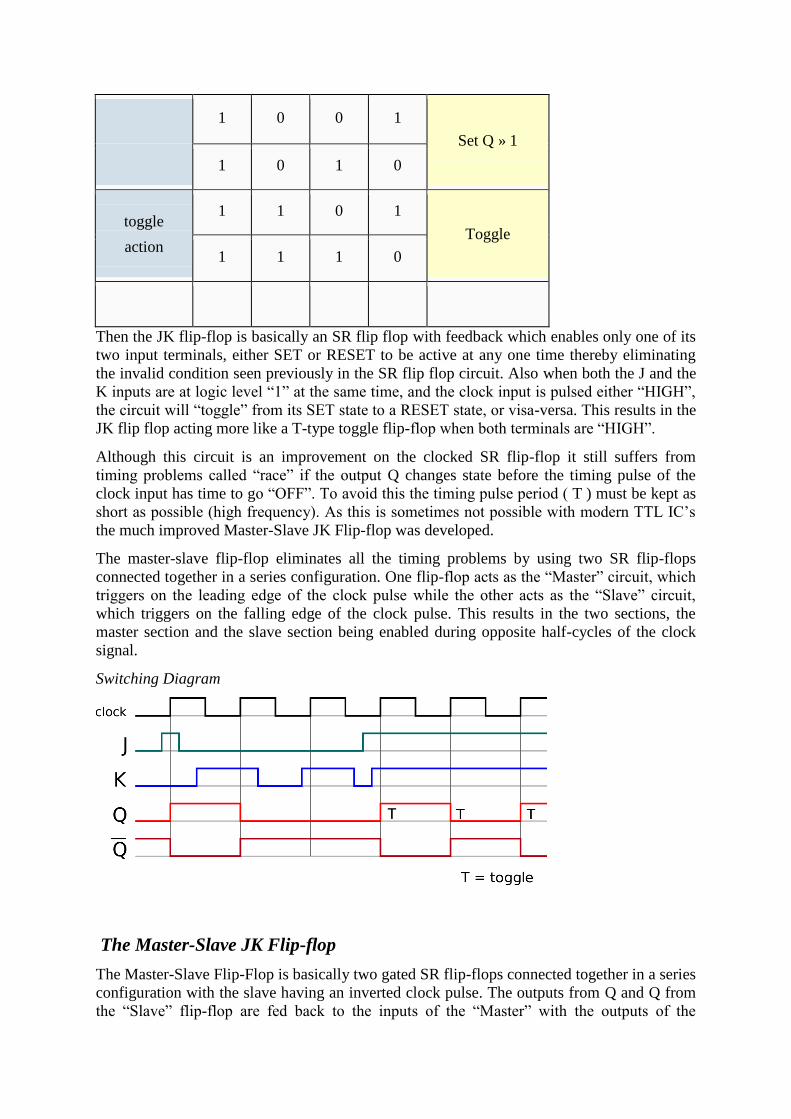
1 0 0 1
Set Q » 1
1 0 1 0
toggle
action
1 1 0 1
Toggle
1 1 1 0
Then the JK flip-flop is basically an SR flip flop with feedback which enables only one of its
two input terminals, either SET or RESET to be active at any one time thereby eliminating
the invalid condition seen previously in the SR flip flop circuit. Also when both the J and the
K inputs are at logic level “1” at the same time, and the clock input is pulsed either “HIGH”,
the circuit will “toggle” from its SET state to a RESET state, or visa-versa. This results in the
JK flip flop acting more like a T-type toggle flip-flop when both terminals are “HIGH”.
Although this circuit is an improvement on the clocked SR flip-flop it still suffers from
timing problems called “race” if the output Q changes state before the timing pulse of the
clock input has time to go “OFF”. To avoid this the timing pulse period ( T ) must be kept as
short as possible (high frequency). As this is sometimes not possible with modern TTL IC’s
the much improved Master-Slave JK Flip-flop was developed.
The master-slave flip-flop eliminates all the timing problems by using two SR flip-flops
connected together in a series configuration. One flip-flop acts as the “Master” circuit, which
triggers on the leading edge of the clock pulse while the other acts as the “Slave” circuit,
which triggers on the falling edge of the clock pulse. This results in the two sections, the
master section and the slave section being enabled during opposite half-cycles of the clock
signal.
Switching Diagram
The Master-Slave JK Flip-flop
The Master-Slave Flip-Flop is basically two gated SR flip-flops connected together in a series
configuration with the slave having an inverted clock pulse. The outputs from Q and Q from
the “Slave” flip-flop are fed back to the inputs of the “Master” with the outputs of the

“Master” flip flop being connected to the two inputs of the “Slave” flip flop. This feedback
configuration from the slave’s output to the master’s input gives the characteristic toggle of
the JK flip flop as shown below.
The Master-Slave JK Flip Flop
The input signals J and K are connected to the gated “master” SR flip flop which “locks” the
input condition while the clock (Clk) input is “HIGH” at logic level “1”. As the clock input of
the “slave” flip flop is the inverse (complement) of the “master” clock input, the “slave” SR
flip flop does not toggle. The outputs from the “master” flip flop are only “seen” by the gated
“slave” flip flop when the clock input goes “LOW” to logic level “0”.
When the clock is “LOW”, the outputs from the “master” flip flop are latched and any
additional changes to its inputs are ignored. The gated “slave” flip flop now responds to the
state of its inputs passed over by the “master” section. Then on the “Low-to-High” transition
of the clock pulse the inputs of the “master” flip flop are fed through to the gated inputs of
the “slave” flip flop and on the “High-to-Low” transition the same inputs are reflected on the
output of the “slave” making this type of flip flop edge or pulse-triggered.
Then, the circuit accepts input data when the clock signal is “HIGH”, and passes the data to
the output on the falling-edge of the clock signal. In other words, the Master-Slave JK Flip
flop is a “Synchronous” device as it only passes data with the timing of the clock signal.
4. The T Flip Flop
This is a much simpler version of the J-K flip flop. Both the J and K inputs are connected together and thus are also called a single input J-K flip flop. When clock pulse is given to the flip flop, the output begins to toggle. Here also the restriction on the pulse width can be eliminated with a master-slave or edge-triggered construction. Take a look at the circuit and truth table below.
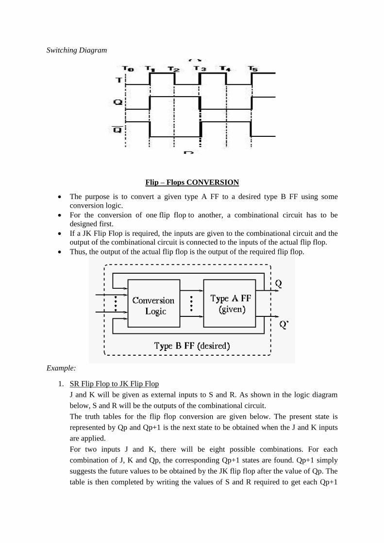
Switching Diagram
Flip – Flops CONVERSION
The purpose is to convert a given type A FF to a desired type B FF using some
conversion logic.
For the conversion of one flip flop to another, a combinational circuit has to be
designed first.
If a JK Flip Flop is required, the inputs are given to the combinational circuit and the
output of the combinational circuit is connected to the inputs of the actual flip flop.
Thus, the output of the actual flip flop is the output of the required flip flop.
Example:
1. SR Flip Flop to JK Flip Flop
J and K will be given as external inputs to S and R. As shown in the logic diagram
below, S and R will be the outputs of the combinational circuit.
The truth tables for the flip flop conversion are given below. The present state is
represented by Qp and Qp+1 is the next state to be obtained when the J and K inputs
are applied.
For two inputs J and K, there will be eight possible combinations. For each
combination of J, K and Qp, the corresponding Qp+1 states are found. Qp+1 simply
suggests the future values to be obtained by the JK flip flop after the value of Qp. The
table is then completed by writing the values of S and R required to get each Qp+1

from the corresponding Qp. That is, the values of S and R that are required to change
the state of the flip flop from Qp to Qp+1 are written.
2. JK Flip Flop to SR Flip Flop
This will be the reverse process of the above explained conversion. S and R will be the
external inputs to J and K. As shown in the logic diagram below, J and K will be the outputs
of the combinational circuit. Thus, the values of J and K have to be obtained in terms of S, R
and Qp. The logic diagram is shown below.
A conversion table is to be written using S, R, Qp, Qp+1, J and K. For two inputs, S and R,
eight combinations are made. For each combination, the corresponding Qp+1 outputs are
found ut. The outputs for the combinations of S=1 and R=1 are not permitted for an SR flip
flop. Thus the outputs are considered invalid and the J and K values are taken as “don’t
cares”.

3. SR Flip Flop to D Flip Flop
As shown in the figure, S and R are the actual inputs of the flip flop and D is the external
input of the flip flop. The four combinations, the logic diagram, conversion table, and the K-
map for S and R in terms of D and Qp are shown below.

4. D Flip Flop to SR Flip Flop
D is the actual input of the flip flop and S and R are the external inputs. Eight
possible combinations are achieved from the external inputs S, R and Qp. But,
since the combination of S=1 and R=1 are invalid, the values of Qp+1 and D are
considered as “don’t cares”. The logic diagram showing the conversion from D to
SR, and the K-map for D in terms of S, R and Qp are shown below.
5. JK Flip Flop to T Flip Flop
J and K are the actual inputs of the flip flop and T is taken as the external input for
conversion. Four combinations are produced with T and Qp. J and K are expressed in terms
of T and Qp. The conversion table, K-maps, and the logic diagram are given below.

6. JK Flip Flop to D Flip Flop
D is the external input and J and K are the actual inputs of the flip flop. D and Qp make
four combinations. J and K are expressed in terms of D and Qp. The four combination
conversion table, the K-maps for J and K in terms of D and Qp, and the logic diagram
showing the conversion from JK to D are given below.
7. D Flip Flop to JK Flip Flop
In this conversion, D is the actual input to the flip flop and J and K are the external inputs.
J, K and Qp make eight possible combinations, as shown in the conversion table below. D
is expressed in terms of J, K and Qp.
The conversion table, the K-map for D in terms of J, K and Qp and the logic diagram
showing the conversion from D to JK are given in the figure below.

Counters
Synchronous
Here, all the flip-flops receive the
external clock pulses externally.
Asynchronous
Here, external clock pulses is applied
to one flip-flop and then output of
preceding flip-flop is connected to the
clock of next flip-flop.
UP Counter
Counts from small to big
count.
Output goes on increasing
as they receive clock pulse
Eg: 0, 1, 2, 3….
Down Counter
Counts from large to
small count.
Output goes on
decreasing as they
receive clock pulse
Eg: .., 7, 6, 5, 4….
UP/ DOWN Counter
Combination of both but at a
time either UP or DOWN
Counter
Asynchronous / Ripple Counters:
A counter that follows the binary sequence is called a binary counter. A binary ripple
counter consists of a series of complementing flip flops (T or JK FF) with the output of each
flip flop connected to the clock pulse input of the next higher order flip flop. The flip flop
holding the least significant bit receives the incoming count pulses.
It is known as ripple counter because the flip flops change one at a time in rapid succession
and the signal propagates through the counter in a ripple fashion. CLK is coming for
subsequent flip flops from previous flip flops and change state only when transition of
previous flip flop’s output is from high to low i.e. from 1 to 0
The complement of the count sequence counts in reverse direction. If the un-complemented
output counts up, the complemented output counts down. If the un-complemented output
counts down, the complemented output counts up.
There are many ways to implement the ripple counter depending on the characteristics of the
flip flops used and the requirements of the count sequence.

Clock Trigger: Positive edged or Negative edged
JK or D flip-flops
Count Direction: Up, Down, or Up/Down
Asynchronous counters are slower than synchronous counters because of the delay in the
transmission of the pulses from flip-flop to flip-flop. With a synchronous circuit, all the bits
in the count change synchronously with the assertion of the clock. Examples of synchronous
counters are the Ring and Johnson counter.
It can be implemented using D-type flip-flops or JK-type flip-flops.
The circuit below uses 2 D flip-flops to implement a divide-by-4 ripple counter (2n = 22 = 4).
It counts down.
Example:
1. UP Counter
2. DOWN Counter
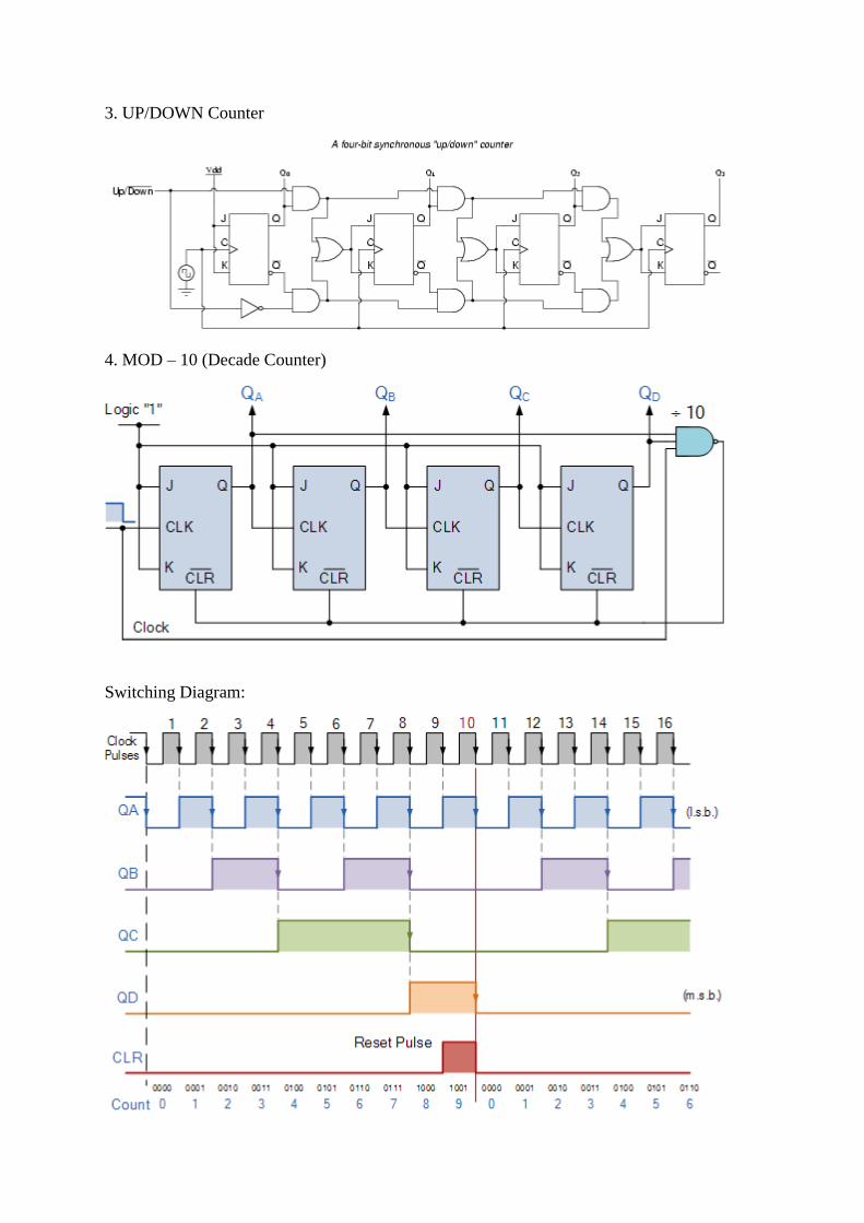
3. UP/DOWN Counter
4. MOD – 10 (Decade Counter)
Switching Diagram:

Synchronous Counters:
A synchronous counter, in contrast to an asynchronous counter, is one whose output bits
change state simultaneously, with no ripple. The only way we can build such a counter circuit
from J-K flip-flops is to connect all the clock inputs together, so that each and every flip-flop
receives the exact same clock pulse at the exact same time.
Example:
1. Binary UP Counter
2. Binary DOWN Counter
3. Binary UP/DOWN Counter

4. MOD-N/Divide-by-N Counters
Normal binary counter counts from 0 to 2N - 1, where N is the number od bits/flip-flops in the
counter. In some cases, we want it to count to numbers other than 2N - 1. This can be done by
allowing the counter to skip states that are normally part of the counting sequence. There are
a few methods of doing this. One of the most common methods is to use the CLEAR input on
the flip-flops.
3-bit Synchronous Binary MOD-6 Counter
In the example above, we have a MOD-6 counter. Without the NAND gate, it is a MOD-8
counter. Now, with the NAND gate, the output from the NAND gate is connected to the
asynchronous CLEAR inputs of each flip-flop. The inputs to the NAND gate are the outputs
of the B and C flip-flops. So, all the flip-flops will be cleared when B = C = 1 (1102 = 610 ).
When the counter goess from state 101 to state 110, the NAND output will immediately clear
the counter to state 000. Once the flip-flops have been cleared, the B = C = 1 condition no
longer exists and the NAND output goes back to high. The counter will therefore count from
000 to 101, and for a very short period of time, be in state 110 before the counter is cleared.
This state is called the temporary state and the counter usually only remains in a temporary
state for a few nanoseconds. We can essentially say that the counter skips 110 and 111 so that
it goes only six different states; thus, it is a MOD-6 counter. We also have to note that the
temporary state causes a spike or glitch on the output waveform of B. This glitch is very
narrow and will not normally be a problem unless it is used to drive other circuitry outside
the counter. The 111 state is the unused state here. In a state machine with unused states, we
need to make sure that the unused states do not cause the system to hang, ie. no way to get
out of the state. We don't have to worry about this here because even if the system does go to
the 111 state, it will go to state 000, a valid state) on the next clock pulse.
RING COUNTER
Ring counters are implemented using shift registers. It is essentially a circulating shift register
connected so that the last flip-flop shifts its value into the first flip-flop. There is usually only
a single 1 circulating in the register, as long as clock pulses are applied.
In the diagram below, assuming a starting state of Q3 = 1 and Q2 = Q1 = Q0 = 0. At the first
pulse, the 1 shifts from Q3 to Q2 and the counter is in the 0100 state. The next pulse produces
the 0010 state and the third, 0001. At the fourth pulse, the 1 at Q0 is transferred back to Q3,
resulting in the 1000 state, which is the initial state. Subsequent pulses will cause the
sequence to repeat, hence the name ring counter.
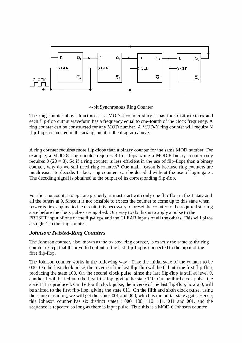
4-bit Synchronous Ring Counter
The ring counter above functions as a MOD-4 counter since it has four distinct states and
each flip-flop output waveform has a frequency equal to one-fourth of the clock frequency. A
ring counter can be constructed for any MOD number. A MOD-N ring counter will require N
flip-flops connected in the arrangement as the diagram above.
A ring counter requires more flip-flops than a binary counter for the same MOD number. For
example, a MOD-8 ring counter requires 8 flip-flops while a MOD-8 binary counter only
requires 3 (23 = 8). So if a ring counter is less efficient in the use of flip-flops than a binary
counter, why do we still need ring counters? One main reason is because ring counters are
much easier to decode. In fact, ring counters can be decoded without the use of logic gates.
The decoding signal is obtained at the output of its corresponding flip-flop.
For the ring counter to operate properly, it must start with only one flip-flop in the 1 state and
all the others at 0. Since it is not possible to expect the counter to come up to this state when
power is first applied to the circuit, it is necessary to preset the counter to the required starting
state before the clock pulses are applied. One way to do this is to apply a pulse to the
PRESET input of one of the flip-flops and the CLEAR inputs of all the others. This will place
a single 1 in the ring counter.
Johnson/Twisted-Ring Counters
The Johnson counter, also known as the twisted-ring counter, is exactly the same as the ring
counter except that the inverted output of the last flip-flop is connected to the input of the
first flip-flop.
The Johnson counter works in the following way : Take the initial state of the counter to be
000. On the first clock pulse, the inverse of the last flip-flop will be fed into the first flip-flop,
producing the state 100. On the second clock pulse, since the last flip-flop is still at level 0,
another 1 will be fed into the first flip-flop, giving the state 110. On the third clock pulse, the
state 111 is produced. On the fourth clock pulse, the inverse of the last flip-flop, now a 0, will
be shifted to the first flip-flop, giving the state 011. On the fifth and sixth clock pulse, using
the same reasoning, we will get the states 001 and 000, which is the initial state again. Hence,
this Johnson counter has six distinct states : 000, 100, 110, 111, 011 and 001, and the
sequence is repeated so long as there is input pulse. Thus this is a MOD-6 Johnson counter.

4-bit Synchronous Johnson Counter
The MOD number of a Johnson counter is twice the number of flip-flops. In the example
above, three flip-flops were used to create the MOD-6 Johnson counter. So for a given MOD
number, a Johnson counter requires only half the number of flip-flops needed for a ring
counter. However, a Johnson counter requires decoding gates whereas a ring counter doesn't.
As with the binary counter, one logic gate (AND gate) is required to decode each state, but
with the Johnson counter, each gate requires only two inputs, regardless of the number of
flip-flops in the counter. Note that we are comparing with the binary counter using the speed
up technique discussed above. The reason for this is that for each state, two of the N flip-
flops used will be in a unique combination of states. In the example above, the combination
Q2 = Q1 = 0 occurs only once in the counting sequence, at the count of 0. The state 010 does
not occur. Thus, an AND gate with inputs (not Q2) and (not Q2) can be used to decode for
this state. The same characteristic is shared by all the other states in the sequence.
A Johnson counters represent a middle ground between ring counters and binary counters. A
Johnson counter requires fewer flip-flops than a ring counter but generally more than a binary
counter; it has more decoding circuitry than a ring counter but less than a binary counter.
Thus, it sometimes represents a logical choice for certain applications.
Synchronous UP/Down Modulo-16 Binary Counter (IC 74193)
The 74193is a 4-bit synchronous binary up/down counter.
Separate up/down clocks, CPU and CPD respectively, simplify operation.
The outputs change state synchronously with the LOW-to-HIGH transition of either
clock input.
If the CPU clock is pulsed while CPD is held HIGH, the device will count up.
If the CPD clock is pulsed while CPU is held HIGH, the device will count down.
Only one clock input can be held HIGH at any time to guarantee predictable behavior.
The device can be cleared at any time by the asynchronous master reset input (MR).
It may also be loaded in parallel by activating the asynchronous parallel load input
(PL).
The terminal count up (TCU) and terminal count down (TCD) outputs are normally
HIGH.
When the circuit has reached the maximum count state of 15, the next HIGH-to-LOW
transition of CPU will cause TCU to go LOW.

TCU will stay LOW until CPU goes HIGH again, duplicating the count up clock.
Likewise, the TCD output will go LOW when the circuit is in the zero state and the
CPD goes LOW.
The terminal count outputs can be used as the clock input signals to the next higher
order circuit in a multistage counter, since they duplicate the clock waveforms.
Multistage counters will not be fully synchronous, since there is a slight delay time
difference added for each stage that is added.
The counter may be preset by the asynchronous parallel load capability of the circuit.
Information present on the parallel data inputs (D0 to D3) is loaded into the counter
and appears on the outputs (Q0 to Q3) regardless of the conditions of the clock inputs
when the parallel load (PL) input is LOW.
A HIGH level on the master reset (MR) input will disable the parallel load gates,
override both clock inputs and set all outputs (Q0 to Q3) LOW.
If one of the clock inputs is LOW during and after a reset or load operation, the next
LOW-to-HIGH transition of that clock will be interpreted as a legitimate signal and
will be counted.
Inputs include clamp diodes. This enables the use of current limiting resistors to
interface inputs to voltages in excess of VCC.
Features and benefits: Input levels:
For 74HC193: CMOS level
For 74HCT193: TTL level
Synchronous reversible 4-bit binary counting
Asynchronous parallel load
Asynchronous reset
Expandable without external logic
Multiple package options
IC 74193 Connection Diagram:
D1 1 • 16 Vcc
Q1 2 15 D0
Q0 3 14 MR
CPD 4 13 TCD
CPU 5 IC 74193 12 TCU
Q2 6 11 PL
Q3 7 10 D2
GND 8 9 D3

Pin detail & Function table:-
Pin Symbol Description
1 D1 data input
2 Q1 counter output
3 Q0 counter output
4 CPD count down clock input (low-to-high, edge-triggered)
5 CPU count up clock input (low-to-high, edge-triggered)
6 Q2 counter output
7 Q3 counter output
8 GND ground
9 D3 data input
10 D2 data input
11 PL parallel load input (active low)
12 TCU terminal count up (carry) output (active low)
13 TCD terminal count down (borrow) output (active low)
14 MR asynchronous master reset (active high)
15 D0 data input
16 Vcc supply voltage
IC 74193 Logic Diagram:

IC 74193 Functional Description:
IC 74193 Typical clear, load and count sequence:

IC 74193 Pesettable UP Counter State Diagram :
IC 74193 Pesettable DOWN Counter State Diagram :
SHIFT REGISTERS
Shift registers, like counters, are a form of sequential logic. Sequential logic, unlike
combinational logic is not only affected by the present inputs, but also, by the prior history.
In other words, sequential logic remembers past events.
Shift registers produce a discrete delay of a digital signal or waveform. A waveform
synchronized to a clock, a repeating square wave, is delayed by "n" discrete clock times,
where "n" is the number of shift register stages. Thus, a four stage shift register delays "data
in" by four clocks to "data out". The stages in a shift register are delay stages, typically
type "D" Flip-Flops or type "JK" Flip-flops.
Formerly, very long (several hundred stages) shift registers served as digital memory. This
obsolete application is reminiscent of the acoustic mercury delay lines used as early computer
memory.
Serial data transmission, over a distance of meters to kilometers, uses shift registers to
convert parallel data to serial form. Serial data communications replaces many slow parallel
data wires with a single serial high speed circuit.
Serial data over shorter distances of tens of centimeters, uses shift registers to get data into
and out of microprocessors. Numerous peripherals, including analog to digital converters,
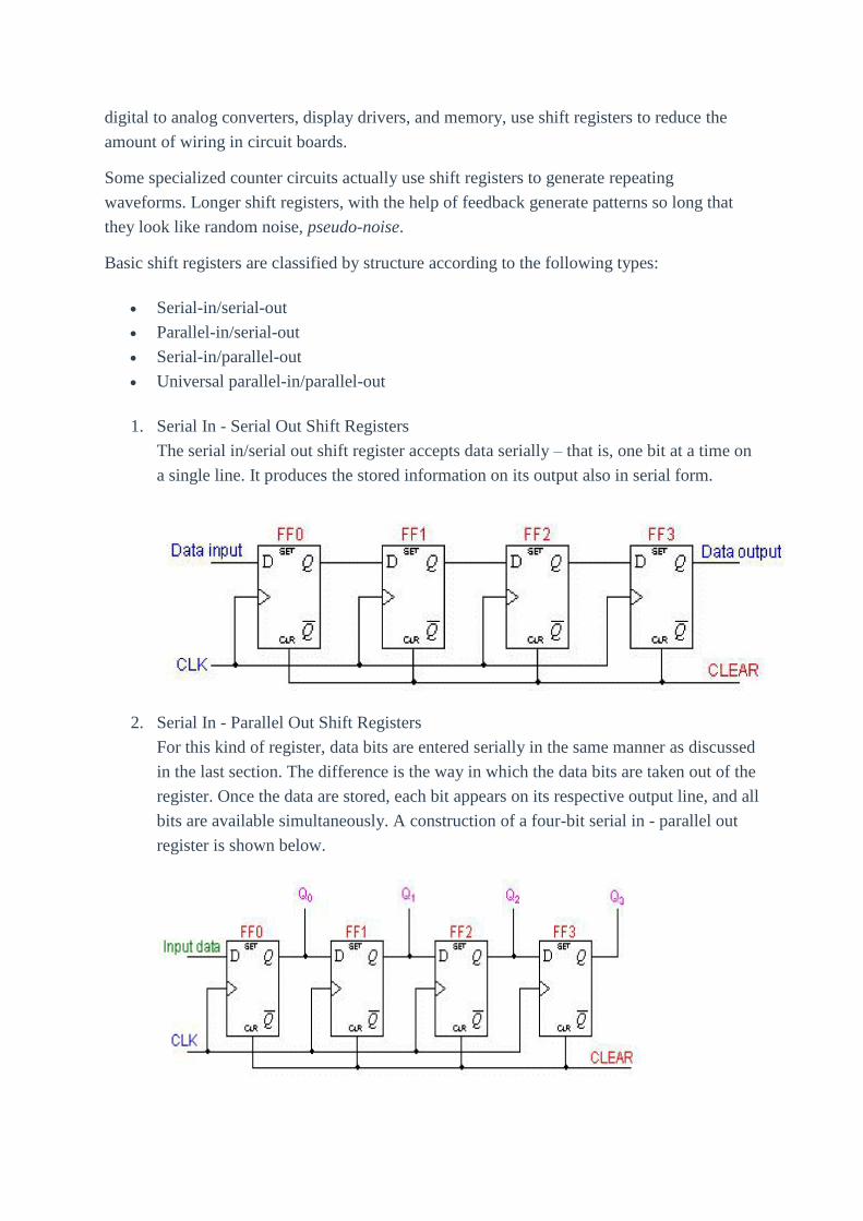
digital to analog converters, display drivers, and memory, use shift registers to reduce the
amount of wiring in circuit boards.
Some specialized counter circuits actually use shift registers to generate repeating
waveforms. Longer shift registers, with the help of feedback generate patterns so long that
they look like random noise, pseudo-noise.
Basic shift registers are classified by structure according to the following types:
Serial-in/serial-out
Parallel-in/serial-out
Serial-in/parallel-out
Universal parallel-in/parallel-out
1. Serial In - Serial Out Shift Registers
The serial in/serial out shift register accepts data serially – that is, one bit at a time on
a single line. It produces the stored information on its output also in serial form.
2. Serial In - Parallel Out Shift Registers
For this kind of register, data bits are entered serially in the same manner as discussed
in the last section. The difference is the way in which the data bits are taken out of the
register. Once the data are stored, each bit appears on its respective output line, and all
bits are available simultaneously. A construction of a four-bit serial in - parallel out
register is shown below.
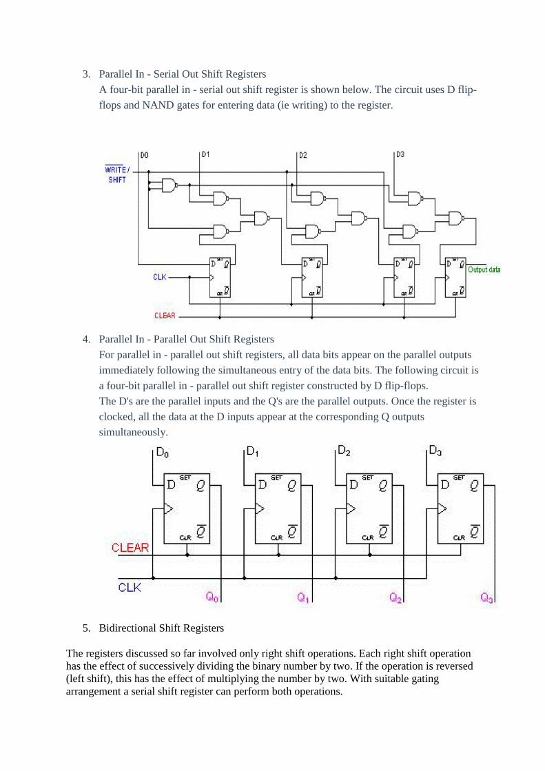
3. Parallel In - Serial Out Shift Registers
A four-bit parallel in - serial out shift register is shown below. The circuit uses D flip-
flops and NAND gates for entering data (ie writing) to the register.
4. Parallel In - Parallel Out Shift Registers
For parallel in - parallel out shift registers, all data bits appear on the parallel outputs
immediately following the simultaneous entry of the data bits. The following circuit is
a four-bit parallel in - parallel out shift register constructed by D flip-flops.
The D's are the parallel inputs and the Q's are the parallel outputs. Once the register is
clocked, all the data at the D inputs appear at the corresponding Q outputs
simultaneously.
5. Bidirectional Shift Registers
The registers discussed so far involved only right shift operations. Each right shift operation
has the effect of successively dividing the binary number by two. If the operation is reversed
(left shift), this has the effect of multiplying the number by two. With suitable gating
arrangement a serial shift register can perform both operations.
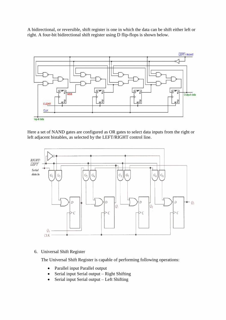
A bidirectional, or reversible, shift register is one in which the data can be shift either left or
right. A four-bit bidirectional shift register using D flip-flops is shown below.
Here a set of NAND gates are configured as OR gates to select data inputs from the right or
left adjacent bistables, as selected by the LEFT/RIGHT control line.
6. Universal Shift Register
The Universal Shift Register is capable of performing following operations:
Parallel input Parallel output
Serial input Serial output – Right Shifting
Serial input Serial output – Left Shifting

5-Bit SHIFT REGISTER (IC 74193)
IC 7496 is a 5−bit shift register in a 16−Lead plastic DIP type package.
It consists of five R−S master−slave flip−flops connected to perform
parallel−to−serial or serial−to−parallel conversion of binary data.
Since both inputs and outputs for all flip−flops are accessible,
parallel−in/parallel−out or serial−in/serial−out operation may be performed.
All flip−flops are simultaneously set to a low output level by applying a low−level
voltage to the clear input while the preset is inactive (low).
Clearing is independent of the level of the clock input.
The register may be parallel loaded by using the clear input in conjunction with the
preset inputs.
After clearing all stages to low output levels, data to be loaded is applied to the
individual preset inputs (A, B, C, D, and E) and a high−level load pulse is applied
to the preset enable input.
Presetting, like clearing, is independent of the level of the clock input.
Transfer of information to the outputs occurs on the positive−going edge of the
clock pulse.
The proper information must be set up at the R−S inputs of each flip−flop prior to
the rising edge of the clock input waveform.
The serial input provides this information to the first flip−flop, while the outputs of
the subsequent flip−flops provide information for the remaining R−S inputs.

The clear input must be high and the preset or preset enable inputs must be low
when clocking occurs.
Features:
N−Bit Serial−to−Parallel Converter
N−Bit Parallel−to−Serial Converter
N−Bit Storage Register
IC 7496 Connection Diagram:
IC 7496 Functional Description:
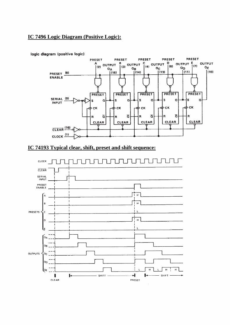
IC 7496 Logic Diagram (Positive Logic):
IC 74193 Typical clear, shift, preset and shift sequence:
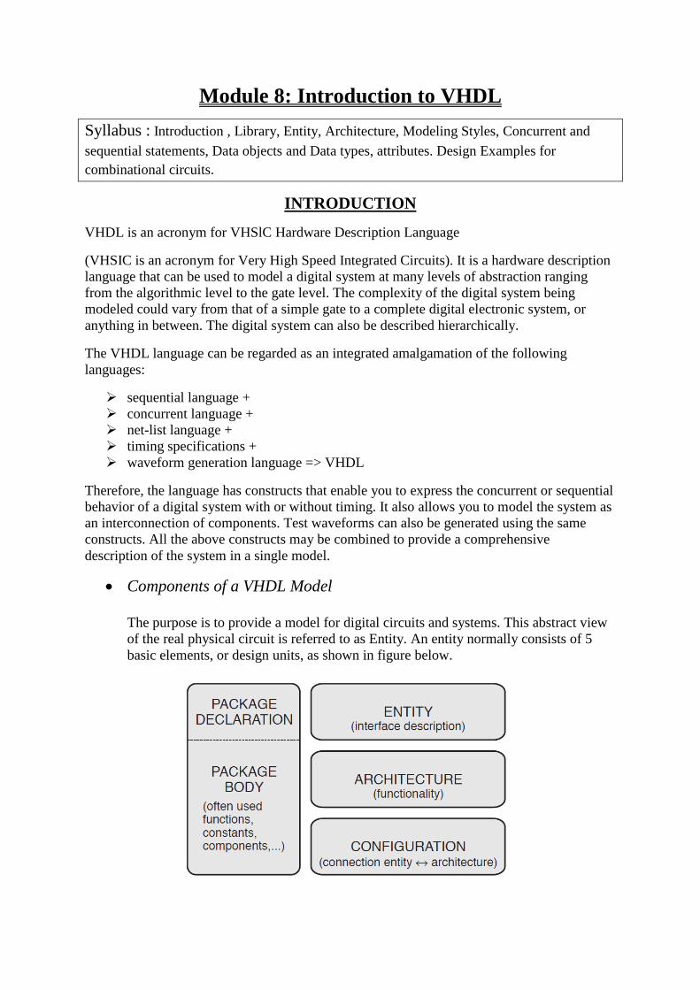
Module 8: Introduction to VHDL
Syllabus : Introduction , Library, Entity, Architecture, Modeling Styles, Concurrent and
sequential statements, Data objects and Data types, attributes. Design Examples for
combinational circuits.
INTRODUCTION
VHDL is an acronym for VHSlC Hardware Description Language
(VHSIC is an acronym for Very High Speed Integrated Circuits). It is a hardware description
language that can be used to model a digital system at many levels of abstraction ranging
from the algorithmic level to the gate level. The complexity of the digital system being
modeled could vary from that of a simple gate to a complete digital electronic system, or
anything in between. The digital system can also be described hierarchically.
The VHDL language can be regarded as an integrated amalgamation of the following
languages:
sequential language +
concurrent language +
net-list language +
timing specifications +
waveform generation language => VHDL
Therefore, the language has constructs that enable you to express the concurrent or sequential
behavior of a digital system with or without timing. It also allows you to model the system as
an interconnection of components. Test waveforms can also be generated using the same
constructs. All the above constructs may be combined to provide a comprehensive
description of the system in a single model.
Components of a VHDL Model
The purpose is to provide a model for digital circuits and systems. This abstract view
of the real physical circuit is referred to as Entity. An entity normally consists of 5
basic elements, or design units, as shown in figure below.

VHDL Terms
These are the basic VHDL building blocks that are used in almost every description,
along with some terms that are redefined in VHDL to mean something different to the
average designer.
Entity. All designs are expressed in terms of entities. An entity is
the most basic building block in a design. The uppermost level of the design is the
top-level entity. If the design is hierarchical, then the top-level description will have
lower-level descriptions contained in it. These lower-level descriptions will be lower-
level entities contained in the top-level entity description.
Architecture. All entities that can be simulated have an architecture
description. The architecture describes the behavior of the entity. A single entity can
have multiple architectures. One architecture might be behavioral while another might
be a structural description of the design.
Configuration. A configuration statement is used to bind a component instance
to an entity-architecture pair. A configuration can be considered like a parts list for a
design. It describes which behavior to use for each entity, much like a parts list
describes which part to use for each part in the design.
Package. A package is a collection of commonly used data types and
subprograms used in a design. Think of a package as a toolbox that contains tools
used to build designs.
Driver. This is a source on a signal. If a signal is driven by two sources, then
when both sources are active, the signal will have two drivers
Bus. The term “bus” usually brings to mind a group of signals or a particular
method of communication used in the design of hardware. In VHDL, a bus is a
special kind of signal that may have its drivers turned off. _
Attribute. An attribute is data that are attached to VHDL objects or
predefined data about VHDL objects. Examples are the current drive capability of
a buffer or the maximum operating temperature of the device.
_ Generic. A generic is VHDL‟s term for a parameter that passes information
to an entity. For instance, if an entity is a gate level model with a rise and a fall delay,
values for the rise and fall delays could be passed into the entity with generics.
Process. A process is the basic unit of execution in VHDL. All operations that
are performed in a simulation of a VHDL description are broken into single or
multiple processes.

Library Declarations:
A LIBRARY is a collection of commonly used pieces of code. Placing such pieces inside a
library allows them to be reused or shared by other designs. The typical structure of a library.
The code is usually written in the form of FUCTIONS, PROCEDURES, or COMPONETS,
which are placed inside PACKAGES and complied into destination library.
To declare a LIBRARY (that is to make it visible to the design) two lines of code are
needed, one containing the name of the library and other a use clause.
library IEEE;
use IEEE.std_logic_1164.all;
use IEEE.std_logic_textio.all;
use IEEE.std_logic_arith.all;
use IEEE.numeric_bit.all;
use IEEE.numeric_std.all;
use IEEE.std_logic_signed.all;
use IEEE.std_logic_unsigned.all;
use IEEE.math_real.all;
use IEEE.math_complex.all;
library STD;
use STD.textio;
Entity
A VHDL entity specifies the name of the entity, the ports of the entity, and entity-related
information. All designs are created using one or more entities. Example
ENTITY mux IS
PORT ( a, b, c, d : IN BIT;
s0, s1 : IN BIT;
x, : OUT BIT);
END mux;
The keyword ENTITY signifies that this is the start of an entity statement. In the descriptions
shown throughout the book, keywords of the language and types provided with the
STANDARD package are shown in ALL CAPITAL letters. For instance, in the preceding
example, the keywords are ENTITY, IS, PORT, IN, INOUT, and so on. The standard type
provided is BIT. Names of user-created objects such as mux, in the example above, will be
shown in lower case.
The name of the entity is mux. The entity has seven ports in the PORT clause. Six ports are
of mode IN and one port is of mode OUT. The four data input ports (a, b, c, d) are of type
BIT. The two multiplexer select inputs, s0 and s1, are also of type BIT. The output port is
of type BIT.
The entity describes the interface to the outside world. It specifies the number of ports, the
direction of the ports, and the type of the ports. A lot more information can be put into the
entity than is shown here, but this gives us a foundation upon which we can build more
complex examples.

Architectures
The entity describes the interface to the VHDL model. The architecture describes the
underlying functionality of the entity and contains the statements that model the behaviour of
the entity. An architecture is always related to an entity and describes the behaviour of that
entity.
An architecture for the counter device described earlier would look like this:

The keyword ARCHITECTURE signifies that this statement describes architecture for an
entity. The architecture name is dataflow. The entity the architecture is describing is called
mux.
The reason for the connection between the architecture and the entity is that an entity can
have multiple architectures describing the behaviour of the entity. For instance, one
architecture could be a behavioral description, and another could be a structural description.
The textual area between the keyword ARCHITECTURE and the keyword BEGIN is
where local signals and components are declared for later use.
In this example signal select is declared to be a local signal. The statement area of the
architecture starts with the keyword BEGIN. All statements between the BEGIN and the
END netlist statement are called concurrent statements, because all the statements execute
concurrently.
Modeling Styles
VHDL provides a broad set of constructs (statements). With VHDL you can describe discrete
electronic systems of varying complexity (systems, boards, chips, modules) with varying
levels of abstraction. VHDL language constructs are divided into different modelling styles
by their level of abstraction:
Behavioral Style
Dataflow Style
Structural Style
Behavioral Style
This style describes a behavior in a “program-like” (procedural) manner, using the process
constructs provided in VHDL. Multiple process statements can be used to describe
concurrency. Notice the following example uses sequential statements inside a process
Example:

Structural Style
In this style, focus is on how components are interconnected rather than the operation of each
fundamental component.
Three features of a structural description
1. Ability to define a list of components
2. Definition of signals to interconnect these components
3. Ability to distinguish between multiple copies of same component using labels
Example
Data Flow Style
This style is convenient for illustrating asynchronous and concurrent events, where the delays
represent actual hardware component delays. It is a realistic way of modeling hardware
dependencies and concurrencies. Notice the following example uses concurrent statements
Concurrent Statements
These statements execute in a simultaneous fashion i.e. in parallel. The main concurrent
statements are:
1. Block Statements
2. Concurrent signal assignment
3. Component instantiation
4. Concurrent procedure call
5. Concurrent assertion
6. Generate Statements

Sequential Statements These statements execute in a procedural fashion i.e. serially, inside a process. The main
sequential statements are:
1. Process statement
2. Wait statement
3. Sequential signal assignment
4. Variable assignment
5. Assertion statement
6. Report statement
7. If statement
8. Case statement
9. Loop statement
10. Null statement
11. Next statement
12. Exit statement
13. Function call
14. Procedure call
VHDL Tutorial
Jan Van der Spiegel
University of Pennsylvania
Department of Electrical and Systems Engineering
VHDL Tutorial
1. Introduction
2. Levels of representation and abstraction
3. Basic Structure of a VHDL file
Behavioral model
Concurrency
Structural description
4. Lexical Elements of VHDL
5. Data Objects: Signals, Variables and Constants
Constant
Variable
Signal
6. Data types
Integer types
Floating-point types
Physical types
Array Type
Record Type
Signal attributes
Scalar attributes
Array attributes

7. Operators
8. Behavioral Modeling: Sequential Statements
Basic Loop statement
While-Loop statement
For-Loop statement
9. Dataflow Modeling – Concurrent Statements
10. Structural Modeling
11. References
Appendix: IEEE Standard Package STD_LOGIC_1164
________________________________________________________________________
This tutorial gives a brief overview of the VHDL language and is mainly intended as a
companion for the Digital Design Laboratory. This writing aims to give the reader a quick
introduction to VHDL and to give a complete or in-depth discussion of VHDL. For a more
detailed treatment, please consult any of the many good books on this topic. Several of these
books are listed in the reference list.
1. Introduction
VHDL stands for VHSIC (Very High Speed Integrated
Circuits) Hardware Description Language. In the mid-1980‟s the U.S. Department of
Defense and the IEEE sponsored the development of this hardware description language with
the goal to develop very high-speed integrated circuit. It has become now one of industry‟s
standard languages used to describe digital systems. The other widely used hardware
description language is Verilog. Both are powerful languages that allow you to describe and
simulate complex digital systems. A third HDL language is ABEL (Advanced Boolean
Equation Language) which was specifically designed for Programmable Logic Devices
(PLD). ABEL is less powerful than the other two languages and is less popular in industry.
This tutorial deals with VHDL, as described by the IEEE standard 1076-1993.
Although these languages look similar as conventional programming languages, there are
some important differences. A hardware description language is inherently parallel, i.e.
commands, which correspond to logic gates, are executed (computed) in parallel, as soon as a
new input arrives. A HDL program mimics the behavior of a physical, usually digital, system.
It also allows incorporation of timing specifications (gate delays) as well as to describe a
system as an interconnection of different components.
2. Levels of representation and abstraction
A digital system can be represented at different levels of abstraction [1]. This keeps the
description and design of complex systems manageable. Figure 1 shows different levels of
abstraction.

Figure 1: Levels of abstraction: Behavioral, Structural and Physical
The highest level of abstraction is the behavioral level that describes a system in terms of
what it does (or how it behaves) rather than in terms of its components and interconnection
between them. A behavioral description specifies the relationship between the input and
output signals. This could be a Boolean expression or a more abstract description such as the
Register Transfer or Algorithmic level. As an example, let us consider a simple circuit that
warns car passengers when the door is open or the seatbelt is not used whenever the car key is
inserted in the ignition lock At the behavioral level this could be expressed as,
Warning = Ignition_on AND ( Door_open OR Seatbelt_off)
The structural level, on the other hand, describes a system as a collection of gates and
components that are interconnected to perform a desired function. A structural description
could be compared to a schematic of interconnected logic gates. It is a representation that is
usually closer to the physical realization of a system. For the example above, the structural
representation is shown in Figure 2 below.
Figure 2: Structural representation of a “buzzer” circuit.
VHDL allows one to describe a digital system at the structural or the behavioral level. The
behavioral level can be further divided into two kinds of styles: Data flow and Algorithmic.
The dataflow representation describes how data moves through the system. This is typically
done in terms of data flow between registers (Register Transfer level). The data flow model
makes use of concurrent statements that are executed in parallel as soon as data arrives at the
input. On the other hand, sequential statements are executed in the sequence that they are
specified. VHDL allows both concurrent and sequential signal assignments that will
determine the manner in which they are executed. Examples of both representations will be
given later.

3. Basic Structure of a VHDL file
A digital system in VHDL consists of a design entity that can contain other entities that are
then considered components of the top-level entity. Each entity is modeled by an entity
declaration and an architecture body. One can consider the entity declaration as the interface
to the outside world that defines the input and output signals, while the architecture body
contains the description of the entity and is composed of interconnected entities, processes
and components, all operating concurrently, as schematically shown in Figure 3 below. In a
typical design there will be many such entities connected together to perform the desired
function.
Figure 3: A VHDL entity consisting of an interface (entity declaration) and a body
(architectural description).
VHDL uses reserved keywords that cannot be used as signal names or identifiers. Keywords
and user-defined identifiers are case insensitive. Lines with comments start with two
adjacent hyphens (--) and will be ignored by the compiler. VHDL also ignores line breaks
and extra spaces. VHDL is a strongly typed language which implies that one has always to
declare the type of every object that can have a value, such as signals, constants and
variables.
a. Entity Declaration
The entity declaration defines the NAME of the entity and lists the input and output ports.
The general form is as follows,
entity NAME_OF_ENTITY is [ generic generic_declarations);] port (signal_names: mode type; signal_names: mode type; : signal_names: mode type); end [NAME_OF_ENTITY] ;
An entity always starts with the keyword entity, followed by its name and the
keyword is. Next are the port declarations using the keyword port. An entity declaration
always ends with the keyword end, optionally [] followed by the name of the entity.
The NAME_OF_ENTITY is a user-selected identifier
signal_names consists of a comma separated list of one or more user-selected
identifiers that specify external interface signals.
mode: is one of the reserved words to indicate the signal direction:
o in – indicates that the signal is an input
o out – indicates that the signal is an output of the entity whose value can
only be read by other entities that use it.
o buffer – indicates that the signal is an output of the entity whose value can
be read inside the entity‟s architecture
o inout – the signal can be an input or an output.
type: a built-in or user-defined signal type. Examples of types are bit, bit_vector,
Boolean, character, std_logic, and std_ulogic.
o bit – can have the value 0 and 1
o bit_vector – is a vector of bit values (e.g. bit_vector (0 to 7)
o std_logic, std_ulogic, std_logic_vector, std_ulogic_vector: can have 9
values to indicate the value and strength of a signal. Std_ulogic and
std_logic are preferred over the bit or bit_vector types.
o boolean – can have the value TRUE and FALSE
o integer – can have a range of integer values
o real – can have a range of real values
o character – any printing character
o time – to indicate time
generic: generic declarations are optional and determine the local constants used
for timing and sizing (e.g. bus widths) the entity. A generic can have a default
value. The syntax for a generic follows,
generic (
constant_name: type [:=value] ;
constant_name: type [:=value] ;
:
constant_name: type [:=value] );
For the example of Figure 2 above, the entity declaration looks as follows.
-- comments: example of the buzzer circuit of fig. 2 entity BUZZER is port (DOOR, IGNITION, SBELT: in std_logic;
WARNING: out std_logic); end BUZZER;
The entity is called BUZZER and has three input ports, DOOR, IGNITION and SBELT and
one output port, WARNING. Notice the use and placement of semicolons! The name
BUZZER is an identifier. Inputs are denoted by the keyword in, and outputs by the
keyword out. Since VHDL is a strongly typed language, each port has a defined type. In this
case, we specified the std_logic type. This is the preferred type of digital signals. In
contrast to the bit type that can only have the values „1‟ and „0‟, the std_logic and std_ulogic
types can have nine values. This is important to describe a digital system accurately including
the binary values 0 and 1, as well as the unknown value X, the uninitialized value U, “-” for

don‟t care, Z for high impedance, and several symbols to indicate the signal strength (e.g. L
for weak 0, H for weak 1, W for weak unknown - see section on Enumerated Types). The
std_logic type is defined in the std_logic_1164 package of the IEEE library. The type defines
the set of values an object can have. This has the advantage that it helps with the creation of
models and helps reduce errors. For instance, if one tries to assign an illegal value to an
object, the compiler will flag the error.
A few other examples of entity declarations follow
Four-to-one multiplexer of which each input is an 8-bit word.
entity mux4_to_1 is port (I0,I1,I2,I3: in std_logic_vector(7 downto 0); SEL: in std_logic_vector (1 downto 0);
OUT1: out std_logic_vector(7 downto 0)); end mux4_to_1;
An example of the entity declaration of a D flip-flop with set and reset inputs is
entity dff_sr is port (D,CLK,S,R: in std_logic;
Q,Qnot: out std_logic); end dff_sr;
b. Architecture body
The architecture body specifies how the circuit operates and how it is implemented. As
discussed earlier, an entity or circuit can be specified in a variety of ways, such as behavioral,
structural (interconnected components), or a combination of the above.
The architecture body looks as follows,
architecture architecture_name of NAME_OF_ENTITY is -- Declarations -- components declarations -- signal declarations -- constant declarations -- function declarations -- procedure declarations -- type declarations
:
begin -- Statements
: end architecture_name;

Behavioral model
The architecture body for the example of Figure 2, described at the behavioral level, is given
below,
architecture behavioral of BUZZER is begin
WARNING <=
(not DOOR and IGNITION) or (not SBELT and IGNITION); end behavioral;
The header line of the architecture body defines the architecture name, e.g. behavioral,
and associates it with the entity, BUZZER. The architecture name can be any legal identifier.
The main body of the architecture starts with the keyword begin and gives the Boolean
expression of the function. We will see later that a behavioral model can be described in
several other ways. The “<= ” symbol represents an assignment operator and assigns the
value of the expression on the right to the signal on the left. The architecture body ends with
an end keyword followed by the architecture name.
A few other examples follow. The behavioral description of a two-input AND gate is shown
below.
entity AND2 is port (in1, in2: in std_logic;
out1: out std_logic); end AND2;
architecture behavioral_2 of AND2 is begin
out1 <= in1 and in2; end behavioral_2;
An example of a two-input XNOR gate is shown below.
entity XNOR2 is port (A, B: in std_logic;
Z: out std_logic); end XNOR2;
architecture behavioral_xnor of XNOR2 is -- signal declaration (of internal signals X, Y) signal X, Y: std_logic; begin
X <= A and B; Y <= (not A) and (not B); Z <= X or Y;
End behavioral_xnor;
The statements in the body of the architecture make use of logic operators. Logic operators
that are allowed are: and, or, nand, nor, xor, xnor and not. In addition, other
types of operators including relational, shift, arithmetic are allowed as well (see section

on Operators). For more information on behavioral modeling see section on Behavioral
Modeling.
Concurrency
It is worth pointing out that the signal assignments in the above examples
are concurrent statements. This implies that the statements are executed when one or more of
the signals on the right hand side change their value (i.e. an event occurs on one of the
signals). For instance, when the input A changes, the internal signals X and Y change values
that in turn causes the last statement to update the output Z. There may be a propagation
delay associated with this change. Digital systems are basically data-driven and an event
which occurs on one signal will lead to an event on another signal, etc. The execution of the
statements is determined by the flow of signal values. As a result, the order in which these
statements are given does not matter (i.e., moving the statement for the output Z ahead of that
for X and Y does not change the outcome). This is in contrast to conventional, software
programs that execute the statements in a sequential or procedural manner.
Structural description
The circuit of Figure 2 can also be described using a structural model that specifies what
gates are used and how they are interconnected. The following example illustrates it.
architecture structural of BUZZER is -- Declarations
component AND2 port (in1, in2: in std_logic; out1: out std_logic); end component; component OR2 port (in1, in2: in std_logic; out1: out std_logic); end component; component NOT1 port (in1: in std_logic; out1: out std_logic); end component; -- declaration of signals used to interconnect gates
signal DOOR_NOT, SBELT_NOT, B1, B2: std_logic; begin -- Component instantiations statements
U0: NOT1 port map (DOOR, DOOR_NOT); U1: NOT1 port map (SBELT, SBELT_NOT); U2: AND2 port map (IGNITION, DOOR_NOT, B1);
U3: AND2 port map (IGNITION, SBELT_NOT, B2); U4: OR2 port map (B1, B2, WARNING);
end structural;
Following the header is the declarative part that gives the components (gates) that are going
to be used in the description of the circuits. In our example, we use a two- input AND gate,
two-input OR gate and an inverter. These gates have to be defined first, i.e. they will need an
entity declaration and architecture body (as shown in the previous example). These can be

stored in one of the packages one refers to in the header of the file (seeLibrary and
Packages below). The declarations for the components give the inputs (e.g. in1, in2) and the
output (e.g. out1). Next, one has to define internal nets (signal names). In our example these
signals are called DOOR_NOT, SBELT_NOT, B1, B2 (see Figure 2). Notice that one always
has to declare the type of the signal.
The statements after the begin keyword gives the instantiations of the components and
describes how these are interconnected. A component instantiation statement creates a new
level of hierarchy. Each line starts with aninstance name (e.g. U0) followed by a colon and
a component name and the keyword port map. This keyword defines how the components
are connected. In the example above, this is done through positional association: DOOR
corresponds to the input, in1 of the NOT1 gate and DOOR_NOT to the output. Similarly, for
the AND2 gate where the first two signals (IGNITION and DOOR_NOT) correspond to the
inputs in1 and in2, respectively, and the signal B1 to the output out1. An alternative way is to
use explicit association between the ports, as shown below.
label: component-name port map (port1=>signal1, port2=> signal2,… port3=>signaln);
U0: NOT1 port map (in1 => DOOR, out1 => DOOR_NOT); U1: NOT1 port map (in1 => SBELT, out1 => SBELT_NOT); U2: AND2 port map (in1 => IGNITION, in2 => DOOR_NOT, out1 => B1); U3: AND2 port map (in1 => IGNITION, in2 => SBELT_NOT, B2); U4: OR2 port map (in1 => B1, in2 => B2, out1 => WARNING);
Notice that the order in which these statements are written has no bearing on the execution
since these statements are concurrent and therefore executed in parallel. Indeed, the
schematic that is described by these statements is the same independent of the order of the
statements.
Structural modeling of design lends itself to hierarchical design, in which one can define
components of units that are used over and over again. Once these components are defined
they can be used as blocks, cells or macros in a higher level entity. This can significantly
reduce the complexity of large designs. Hierarchical design approaches are always preferred
over flat designs. We will illustrate the use of a hierarchical design approach for a 4-bit adder,
shown in Figure 4 below. Each full adder can be described by the Boolean expressions for the
sum and carry out signals,
sum = (A B) C
carry = AB + C(A B)
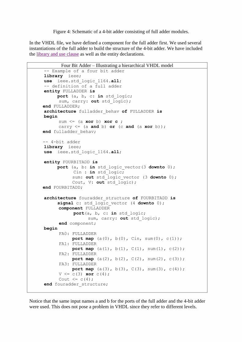
Figure 4: Schematic of a 4-bit adder consisting of full adder modules.
In the VHDL file, we have defined a component for the full adder first. We used several
instantiations of the full adder to build the structure of the 4-bit adder. We have included
the library and use clause as well as the entity declarations.
Four Bit Adder – Illustrating a hierarchical VHDL model -- Example of a four bit adder library ieee; use ieee.std_logic_1164.all; -- definition of a full adder entity FULLADDER is port (a, b, c: in std_logic;
sum, carry: out std_logic); end FULLADDER;
architecture fulladder_behav of FULLADDER is begin
sum <= (a xor b) xor c ; carry <= (a and b) or (c and (a xor b));
end fulladder_behav; -- 4-bit adder
library ieee; use ieee.std_logic_1164.all;
entity FOURBITADD is port (a, b: in std_logic_vector(3 downto 0); Cin : in std_logic;
sum: out std_logic_vector (3 downto 0); Cout, V: out std_logic); end FOURBITADD;
architecture fouradder_structure of FOURBITADD is signal c: std_logic_vector (4 downto 0);
component FULLADDER port(a, b, c: in std_logic;
sum, carry: out std_logic); end component;
begin FA0: FULLADDER port map (a(0), b(0), Cin, sum(0), c(1)); FA1: FULLADDER port map (a(1), b(1), C(1), sum(1), c(2)); FA2: FULLADDER port map (a(2), b(2), C(2), sum(2), c(3)); FA3: FULLADDER port map (a(3), b(3), C(3), sum(3), c(4)); V <= c(3) xor c(4); Cout <= c(4);
end fouradder_structure;
Notice that the same input names a and b for the ports of the full adder and the 4-bit adder
were used. This does not pose a problem in VHDL since they refer to different levels.

However, for readability, it may be easier to use different names. We needed to define the
internal signals c(4:0) to indicate the nets that connect the output carry to the input carry of
the next full adder. For the first input we used the input signal Cin. For the last carry we
defined c(4) as an internal signal since the last carry is needed as the input to the xor gate. We
could not use the output signal Cout since VHDL does not allow the use of outputs as
internal signals! For this reason we had to define the internal carry c(4) and assign c(4) to the
output carry signal Cout.
See also the section on Structural Modeling.
c. Library and Packages: library and use keywords
A library can be considered as a place where the compiler stores information about a design
project. A VHDL package is a file or module that contains declarations of commonly used
objects, data type, component declarations, signal, procedures and functions that can be
shared among different VHDL models.
We mentioned earlier that std_logic is defined in the package ieee.std_logic_1164 in the ieee
library. In order to use the std_logic one needs to specify the library and package. This is
done at the beginning of the VHDL file using the library and the use keywords as
follows:
library ieee; use ieee.std_logic_1164.all;
The .all extension indicates to use all of the ieee.std_logic_1164 package.
The Xilinx Foundation Express comes with several packages.
ieee Library:
std_logic_1164 package: defines the standard datatypes
std_logic_arith package: provides arithmetic, conversion and comparison functions
for the signed, unsigned, integer, std_ulogic, std_logic and std_logic_vector types
std_logic_unsigned
std_logic_misc package: defines supplemental types, subtypes, constants and
functions for the std_logic_1164 package.
To use any of these one must include the library and use clause:
library ieee;
use ieee.std_logic_1164.all;
use ieee.std_logic_arith.all;
use ieee.std_logic_unsigned.all;
In addition, the synopsis library has the attributes package:
library SYNOPSYS;
use SYNOPSYS.attributes.all;
One can add other libraries and packages. The syntax to declare a package is as follows:

-- Package declaration package name_of_package is package declarations end package name_of_package; -- Package body declarations
package body name_of_package is package body declarations end package body name_of_package;
For instance, the basic functions of the AND2, OR2, NAND2, NOR2, XOR2, etc.
components need to be defined before one can use them. This can be done in a package, e.g.
basic_func for each of these components, as follows:
-- Package declaration library ieee; use ieee.std_logic_1164.all;
package basic_func is -- AND2 declaration component AND2 generic (DELAY: time :=5ns); port (in1, in2: in std_logic; out1: out std_logic); end component; -- OR2 declaration
component OR2 generic (DELAY: time :=5ns); port (in1, in2: in std_logic; out1: out std_logic); end component;
end package basic_func; -- Package body declarations library ieee; use ieee.std_logic_1164.all;
package body basic_func is -- 2 input AND gate
entity AND2 is generic (DELAY: time); port (in1, in2: in std_logic; out1: out std_logic); end AND2; architecture model_conc of AND2 is begin out1 <= in1 and in2 after DELAY; end model_conc;
-- 2 input OR gate
entity OR2 is generic (DELAY: time); port (in1, in2: in std_logic; out1: out std_logic); end OR2; architecture model_conc2 of AND2 is begin out1 <= in1 or in2 after DELAY; end model_conc2;
end package body basic_func;

Notice that we included a delay of 5 ns. However, it should be noticed that delay
specifications are ignored by the Foundation synthesis tool. We made use of the predefined
type std_logic that is declared in the package std_logic_1164. We have included
the library and use clause for this package. This package needs to be compiled and
placed in a library. Lets call this library my_func. To use the components of this package one
has to declare it using the library and use clause:
library ieee, my_func; use ieee.std_logic_1164.all, my_func.basic_func.all;
One can concatenate a series of names separated by periods to select a package. The library
and use statements are connected to the subsequent entity statement.
The library and use statements have to be repeated for each entity declaration.
One has to include the library and use clause for each entity as shown for the example of
the four-bit adder above.
4. Lexical Elements of VHDL
a. Identifiers
Identifiers are user-defined words used to name objects in VHDL models. We have seen
examples of identifiers for input and output signals as well as the name of a design entity
and architecture body. When choosing an identifier one needs to follow these basic rules:
May contain only alpha-numeric characters (A to Z, a to z, 0-9) and the
underscore (_) character
The first character must be a letter and the last one cannot be an underscore.
An identifier cannot include two consecutive underscores.
An identifier is case insensitive (ex. And2 and AND2 or and2 refer to the same
object)
An identifier can be of any length.
Examples of valid identifiers are: X10, x_10, My_gate1.
Some invalid identifiers are: _X10, my_gate@input, gate-input.
The above identifiers are called basic identifiers. The rules for these basic identifiers are often
too restrictive to indicate signals. For example, if one wants to indicate an active low signal
such as an active low RESET, one cannot call it /RESET. In order to overcome these
limitations, there are a set of extended identifier rules which allow identifiers with any
sequence of characters.
An extended identifier is enclosed by the backslash, “\”, character.
An extended identifier is case sensitive.
An extended identifier is different from reserved words (keywords) or any basic
identifier (e.g. the identifier \identity\ is allowed)
Inside the two backslashes one can use any character in any order, except that a
backslash as part of an extended identifier must be indicated by an additional

backslash. As an example, to use the identifier BUS:\data, one
writes: \BUS:\data\
Extended identifiers are allowed in the VHDL-93 version but not in VHDL-87
Some examples of legal identifiers are:
Input, \Input\, \input#1\, \Rst\\as\
b. Keywords (Reserved words)
Certain identifiers are used by the system as keywords for special use such as specific
constructs. These keywords cannot be used as identifiers for signals or objects we define. We
have seen several of these reserved words already such as in, out, or, and, port, map, end, etc.
Keywords are often printed in boldface, as is done in this tutorial. For a list of all the
keywords click on complete keyword list. Extended identifiers can make use of keywords
since these are considered different words (e.g. the extended identifier \end\ is allowed.
c. Numbers
The default number representation is the decimal system. VHDL allows integer literals and
real literals. Integer literals consist of whole numbers without a decimal point, while real
literals always include a decimal point. Exponential notation is allowed using the letter “E”
or “e”. For integer literals the exponent must always be positive. Examples are:
Integer literals: 12 10 256E3 12e+6
Real literals: 1.2 256.24 3.14E-2
The number –12 is a combination of a negation operator and an integer literal.
To express a number in a base different from the base “10”, one uses the following
convention: base#number#. A few examples follow.
Base 2: 2#10010# (representing the decimal number “18”)
Base 16: 16#12#
Base 8: 8#22#
Base 2: 2#11101# (representing the decimal number “29”)
Base 16: 16#1D#
Base 8: 8#35#
To make the readability of large numbers easier, one can insert underscores in the numbers as
long as the underscore is not used at the beginning or the end.
2#1001_1101_1100_0010#
215_123
d. Characters, Strings and Bit Strings
To use a character literal in a VHDL code, one puts it in a single quotation mark, as shown in
the examples below:

„a‟, „B‟, „,‟
On the other hand, a string of characters are placed in double quotation marks as shown in
the following examples:
“This is a string”,
“To use a double quotation mark inside a string, use two double quotation marks”
“This is a “”String””.”
Any printing character can be included inside a string.
A bit-string represents a sequence of bit values. In order to indicate that this is a bit string,
one places the „B‟ in front of the string: B”1001”. One can also use strings in the hexagonal
or octal base by using the X or O specifiers, respectively. Some examples are:
Binary: B”1100_1001”, b”1001011”
Hexagonal: X”C9”, X”4b”
Octal: O”311”, o”113”
Notice that in the hexadecimal system, each digit represents exactly 4 bits. As a result, the
number b”1001011” is not the same as X”4b” since the former has only 7 bits while the latter
represents a sequence 8 bits. For the same reason, O”113” (represents 9 bits) is not the same
sequence as X”4b” (represents 8 bits).
5. Data Objects: Signals, Variables and Constants
A data object is created by an object declaration and has a value and type associated with it.
An object can be a Constant, Variable, Signal or a File. Up to now we have seen signals that
were used as input or output ports or internal nets. Signals can be considered wires in a
schematic that can have a current value and future values, and that are a function of the
signal assignment statements. On the other hand, Variables and Constants are used to model
the behavior of a circuit and are used in processes, procedures and functions, similarly as
they would be in a programming language. Following is a brief discussion of each class of
objects.
Constant
A constant can have a single value of a given type and cannot be changed during the
simulation. A constant is declared as follows,
constant list_of_name_of_constant: type [ := initial value] ;
where the initial value is optional. Constants can be declared at the start of an architecture
and can then be used anywhere within the architecture. Constants declared within a process
can only be used inside that specificprocess.
constant RISE_FALL_TME: time := 2 ns; constant DELAY1: time := 4 ns; constant RISE_TIME, FALL_TIME: time:= 1 ns; constant DATA_BUS: integer:= 16;
Variable
A variable can have a single value, as with a constant, but a variable can be updated using a
variable assignment statement. The variable is updated without any delay as soon as the
statement is executed. Variables must be declared inside a process (and are local to the
process). The variable declaration is as follows:
variable list_of_variable_names: type [ := initial value] ;
A few examples follow:
variable CNTR_BIT: bit :=0; variable VAR1: boolean :=FALSE; variable SUM: integer range 0 to 256 :=16; variable STS_BIT: bit_vector (7 downto 0);
The variable SUM, in the example above, is an integer that has a range from 0 to 256 with
initial value of 16 at the start of the simulation. The fourth example defines a bit vector or 8
elements: STS_BIT(7), STS_BIT(6),… STS_BIT(0).
A variable can be updated using a variable assignment statement such as
Variable_name := expression;
As soon as the expression is executed, the variable is updated without any delay.
Signal
Signals are declared outside the process using the following statement:
signal list_of_signal_names: type [ := initial value] ;
signal SUM, CARRY: std_logic;
signal CLOCK: bit; signal TRIGGER: integer :=0; signal DATA_BUS: bit_vector (0 to 7); signal VALUE: integer range 0 to 100;
Signals are updated when their signal assignment statement is executed, after a certain delay,
as illustrated below,
SUM <= (A xor B) after 2 ns;
If no delay is specified, the signal will be updated after a delta delay. One can also specify
multiple waveforms using multiple events as illustrated below,
signal wavefrm : std_logic;
wavefrm <= „0‟, „1‟ after 5ns, „0‟ after 10ns, „1‟ after 20 ns;
It is important to understand the difference between variables and signals, particularly how it
relates to when their value changes. A variable changes instantaneously when the variable
assignment is executed. On the other hand, a signal changes a delay after the assignment
expression is evaluated. If no delay is specified, the signal will change after a delta delay.

This has important consequences for the updated values of variables and signals. Lets
compare the two files in which a process is used to calculate the signal RESULT [7].
Example of a process using Variables
architecture VAR of EXAMPLE is signal TRIGGER, RESULT: integer := 0; begin process variable variable1: integer :=1; variable variable2: integer :=2; variable variable3: integer :=3; begin wait on TRIGGER; variable1 := variable2; variable2 := variable1 + variable3; variable3 := variable2; RESULT <= variable1 + variable2 + variable3; end process;
end VAR
Example of a process using Signals
architecture SIGN of EXAMPLE is signal TRIGGER, RESULT: integer := 0;
signal signal1: integer :=1; signal signal2: integer :=2; signal signal3: integer :=3; begin process begin wait on TRIGGER; signal1 <= signal2; signal2 <= signal1 + signal3; signal3 <= signal2; RESULT <= signal1 + signal2 + signal3; end process; end SIGN;
In the first case, the variables “variable1, variable2 and variable3” are
computed sequentially and their values updated instantaneously after the TRIGGER signal
arrives. Next, the RESULT, which is a signal, is computed using the new values of the
variables and updated a time delta after TRIGGER arrives. This results in the following
values (after a time TRIGGER): variable1 = 2, variable2 = 5 (=2+3), variable3= 5. Since
RESULT is a signal it will be computed at the time TRIGGER and updated at the time
TRIGGER + Delta. Its value will be RESULT=12.
On the other hand, in the second example, the signals will be computed at the time
TRIGGER. All of these signals are computed at the same time, using the old values of
signal1, 2 and 3. All the signals will be updated at Delta time after the TRIGGER has arrived.
Thus the signals will have these values: signal1= 2, signal2= 4 (=1+3), signal3=2 and
RESULT=6.

6. Data types
Each data object has a type associated with it. The type defines the set of values that the
object can have and the set of operations that are allowed on it. The notion of type is key to
VHDL since it is a strongly typed language that requires each object to be of a certain type.
In general one is not allowed to assign a value of one type to an object of another data type
(e.g. assigning an integer to a bit type is not allowed). There are four classes of data types:
scalar, composite, access and file types. The scalar types represent a single value and are
ordered so that relational operations can be performed on them. The scalar type includes
integer, real, and enumerated types of Boolean and Character. Examples of these will be
given further on.
a. Data Types defined in the Standard Package
VHDL has several predefined types in the standard package as shown in the table below. To
use this package one has to include the following clause:
library std, work; use std.standard.all;

Types defined in the Package Standard of the std Library
Type Range of values Example bit „0‟, „1‟ signal A: bit :=1; bit_vector an array with each element of type
bit signal INBUS: bit_vector(7 downto
0); boolean FALSE, TRUE variable TEST: Boolean :=FALSE‟ character any legal VHDL character (see
package standard); printable
characters must be placed between
single quotes (e.g. „#‟)
variable VAL: character :=‟$‟;
file_open_kind* read_mode, write_mode,
append_mode
file_open_status* open_ok, status_error, name_error,
mode_error
integer range is implementation dependent
but includes at least –(231
– 1) to
+(231
– 1)
constant CONST1: integer :=129;
natural integer starting with 0 up to the max
specified in the implementation variable VAR1: natural :=2;
positive integer starting from 1 up the max
specified in the implementation variable VAR2: positive :=2;
real* floating point number in the range
of –1.0 x 1038
to +1.0x 1038
(can be
implementation dependent. Not
supported by the Foundation
synthesis program.
variable VAR3: real :=+64.2E12;
severity_level note, warning, error, failure
string array of which each element is of
the type character variable VAR4: string(1 to 12):=
“@$#ABC*()_%Z”; time* an integer number of which the
range is implementation defined;
units can be expressed in sec, ms,
us, ns, ps, fs, min and hr. . Not
supported by the Foundation
synthesis program
variable DELAY: time :=5 ns;
* Not supported by the Foundation synthesis program
b. User-defined Types
One can introduce new types by using the type declaration, which names the type and
specifies its value range. The syntax is
type identifier is type_definition;
Here are a few examples of type definitions,
Integer types
type small_int is range 0 to 1024;
type my_word_length is range 31 downto 0;
subtype data_word is my_word_length range 7 downto 0;

A subtype is a subset of a previously defined type. The last example above illustrates the use
of subtypes. It defines a type called data_word that is a sybtype of my_word_length of which
the range is restricted from 7 to 0. Another example of a subtype is,
subtype int_small is integer range -1024 to +1024;
Floating-point types
type cmos_level is range 0.0 to 3.3;
type pmos_level is range -5.0 to 0.0;
type probability is range 0.0 to 1.0;
subtype cmos_low_V is cmos_level range 0.0 to +1.8;
Note that floating point data types are not supported by the Xilinx Foundation synthesis
program.
Physical types
The physical type definition includes a units identifier as follows,
type conductance is range 0 to 2E-9 units mho;
mmho = 1E-3 mho; umho = 1E-6 mho; nmho = 1E-9 mho; pmho = 1E-12 mho; end units conductance;
Here are some object declarations that use the above types,
variable BUS_WIDTH: small_int :=24;
signal DATA_BUS: my_word_length;
variable VAR1: cmos_level range 0.0 to 2.5;
constant LINE_COND: conductance:= 125 umho;
Notice that a space must be left before the unit name.
The physical data types are not supported by the Xilinx Foundation Express synthesis
program.
In order to use our own types, we need either to include the type definition inside an
architecture body or to declare the type in a package. The latter can be done as follows for a
package called “my_types”.
package my_types is type small_int is range 0 to 1024; type my_word_length is range 31 downto 0; subtype data_word is my_word_length is range 7 downto 0; type cmos_level is range 0.0 to 3.3;
type conductance is range 0 to 2E-9

units mho;
mmho = 1E-3 mho; umho = 1E-6 mho; nmho = 1E-9 mho; pmho = 1E-12 mho; end units conductance; end package my_types;
c. Enumerated Types
An enumerated type consists of lists of character literals or identifiers. The enumerated type
can be very handy when writing models at an abstract level. The syntax for an enumerated
type is,
type type_name is (identifier list or character literal);
Here are some examples,
type my_3values is („0‟, „1‟, „Z‟);
type PC_OPER is (load, store, add, sub, div, mult, shiftl, shiftr);
type hex_digit is („0‟, „1‟, „2‟, „3‟, „4‟, „5‟, „6‟, „7‟, 8‟, „9‟, „A‟, „B‟, „C‟, „D‟, „E‟, „F‟);
type state_type is (S0, S1, S2, S3);
Examples of objects that use the above types:
signal SIG1: my_3values;
variable ALU_OP: pc_oper;
variable first_digit: hex_digit :=‟0‟;
signal STATE: state_type :=S2;
If one does not initialize the signal, the default initialization is the leftmost element of the list.
Enumerated types have to be defined in the architecture body or inside a package as shown in
the section above.
An example of an enumerated type that has been defined in the std_logic_1164 package is the
std_ulogic type, defined as follows
type STD_ULOGIC is (
„U‟, -- uninitialized
„X‟, -- forcing unknown
„0‟, -- forcing 0
„1‟, -- forcing 1
„Z‟, -- high impedance
„W‟, -- weak unknown
„L‟, -- weak 0
„H‟. -- weak 1
„-„); -- don‟t care
In order to use this type one has to include the clause before each entity declaration.

library ieee; use ieee.std_logic_1164.all;
It is possible that multiple drivers are driving a signal. In that case there could be a conflict
and the output signal would be undetermined. For instance, the outputs of an AND gate and
NOT gate are connected together into the output net OUT1. In order to resolve the value of
the output, one can call up a resolution function. These are usually a user-written function
that will resolve the signal. If the signal is of the type std_ulogic and has multiple drivers, one
needs to use a resolution function. The std_logic_1164 package has such a resolution
function, called RESOLVED predefined. One can then use the following declaration for
signal OUT1
signal OUT1: resolved: std_ulogic;
If there is contention, the RESOLVED function will be used to intermediate the conflict and
determine the value of the signal. Alternatively, one can declare the signal directly as a
std_logic type since the subtype std_logic has been defined in the std_logic_1164 package.
signal OUT1: std_logic;
d. Composite Types: Array and Record
Composite data objects consist of a collection of related data elements in the form of
an array or record. Before we can use such objects one has to declare the composite type
first.
Array Type
An array type is declared as follows:
type array_name is array (indexing scheme) of element_type;
type MY_WORD is array (15 downto 0) of std_logic;
type YOUR_WORD is array (0 to 15) of std_logic;
type VAR is array (0 to 7) of integer;
type STD_LOGIC_1D is array (std_ulogic) of std_logic;
In the first two examples above we have defined a one-dimensional array of elements of the
type std_logic indexed from 15 down to 0, and 0 up to 15, respectively. The last example
defines a one-dimensional array of the type std_logic elements that uses the type std_ulogic
to define the index constraint. Thus this array looks as follows:
Index: ‘U’ ‘X’ ‘0’ ‘1’ ‘Z’ ‘W’ ‘L’ ‘H’ ‘-‘
Element:
We can now declare objects of these data types. Some examples are given
signal MEM_ADDR: MY_WORD;
signal DATA_WORD: YOUR_WORD := B“1101100101010110”;
constant SETTING: VAR := (2,4,6,8,10,12,14,16);

In the first example, the signal MEM_ADDR is an array of 16 bits, initialized to all „0‟s. To
access individual elements of an array we specify the index. For example, MEM_ACCR(15)
accesses the left most bit of the array, while DATA_WORD(15) accesses the right most bit of
the array with value „0‟. To access a subrange, one specifies the index range,
MEM_ADDR(15 downto 8) or DATA_WORD(0 to 7).
Multidimensional arrays can be declared as well by using a similar syntax as above,
type MY_MATRIX3X2 is array (1 to 3, 1 to 2) of natural;
type YOUR_MATRIX4X2 is array (1 to 4, 1 to 2) of integer;
type STD_LOGIC_2D is array (std_ulogic, std_ulogic) of std_logic;
variable DATA_ARR: MY_MATRIX :=((0,2), (1,3), (4,6), (5,7));
The variable array DATA_ARR will then be initialized to,
0 2
1 3 4 6
5 7
To access an element one specifies the index, e.g. DATA_ARR(3,1) returns the value 4.
The last example defines a 9x9 array or table with an index the elements of the std_ulogic
type.
Sometimes it is more convenient not to specify the dimension of the array when the array
type is declared. This is called an unconstrained array type. The syntax for the array
declaration is,
type array_name is array (type range <>) of element_type;
Some examples are
type MATRIX is array (integer range <>) of integer;
type VECTOR_INT is array (natural range <>) of integer;
type VECTOR2 is array (natural range <>, natural range <>) of std_logic;
The range is now specified when one declares the array object,
variable MATRIX8: MATRIX (2 downto -8) := (3, 5, 1, 4, 7, 9, 12, 14, 20, 18);
variable ARRAY3x2: VECTOR2 (1 to 4, 1 to 3)) := ((„1‟,‟0‟), („0‟,‟-„), (1, „Z‟));
Record Type
A second composite type is the records type. A record consists of multiple elements that may
be of different types. The syntax for a record type is the following:
type name is
record identifier :subtype_indication;

:
identifier :subtype_indication;
end record;
As an example,
type MY_MODULE is
record RISE_TIME :time;
FALL_TIME : time;
SIZE : integer range 0 to 200;
DATA : bit_vector (15 downto 0);
end record;
signal A, B: MY_MODULE;
To access values or assign values to records, one can use one of the following methods:
A.RISE_TIME <= 5ns;
A.SIZE <= 120;
B <= A;
e. Type Conversions
Since VHDL is a strongly typed language one cannot assign a value of one data type to a
signal of a different data type. In general, it is preferred to the same data types for the signals
in a design, such as std_logic (instead of a mix of std_logic and bit types). Sometimes one
cannot avoid using different types. To allow assigning data between objects of different
types, one needs to convert one type to the other. Fortunately there are functions available in
several packages in the ieee library, such as the std_logic_1164 and the std_logic_arith
packages. As an example, the std_logic_1164 package allows the following conversions:
Conversions supported by std_logic_1164 package
Conversion Function
std_ulogic to bit to_bit(expression)
std_logic_vector to bit_vector to_bitvector(expression)
std_ulogic_vector to bit_vector to_bitvector(expression)
bit to std_ulogic To_StdULogic(expression)
bit_vector to std_logic_vector To_StdLogicVector(expression)
bit_vector to std_ulogic_vector To_StdUlogicVector(expression)
std_ulogic to std_logic_vector To_StdLogicVector(expression)
std_logic to std_ulogic_vector To_StdUlogicVector(expression)
The IEEE std_logic_unsigned and the IEEE std_logic_arith packages allow additional
conversions such as from an integer to std_logic_vector and vice versa.
An example follows.

entity QUAD_NAND2 is port (A, B: in bit_vector(3 downto 0);
out4: out std_logic_vector (3 downto 0)); end QUAD_NAND2;
architecture behavioral_2 of QUAD_NAND2 is begin
out4 <= to_StdLogicVector(A and B); end behavioral_2;
The expression “A and B” which is of the type bit_vector has to be converted to the type
std_logic_vector to be of the same type as the output signal out4. The syntax of a type conversion is as follows:
type_name (expression);
In order for the conversion to be legal, the expression must return a type that can be
converted into the type type_name. Here are the conditions that must be fulfilled for the
conversion to be possible.
Type conversions between integer types or between similar array types are
possible
Conversion between array types is possible if they have the same length and if
they have identical element types or convertible element types.
Enumerated types cannot be converted.
f. Attributes
VHDL supports 5 types of attributes. Predefined attributes are always applied to a prefix such
as a signal name, variable name or a type. Attributes are used to return various types of
information about a signal, variable or type. Attributes consist of a quote mark („) followed
by the name of the attribute.
Signal attributes
The following table gives several signal attributes.
Attribute Function
signal_name’event returns the Boolean value True if an event on the
signal occurred, otherwise gives a False
signal_name’active returns the Boolean value True there has been a
transaction (assignment) on the signal, otherwise
gives a False
signal_name’transaction returns a signal of the type “bit” that toggles (0 to 1
or 1 to 0) every time there is a transaction on the
signal.
signal_name’last_event returns the time interval since the last event on the
signal

signal_name’last_active returns the time interval since the last transaction
on the signal
signal_name’last_value gives the value of the signal before the last event
occurred on the signal
signal_name’delayed(T) gives a signal that is the delayed version (by time
T) of the original one. [T is optional, default T=0]
signal_name’stable(T) returns a Boolean value, True, if no event has
occurred on the signal during the interval T,
otherwise returns a False. [T is optional, default
T=0]
signal_name’quiet(T) returns a Boolean value, True, if no transaction has
occurred on the signal during the interval T,
otherwise returns a False. [T is optional, default
T=0]
An example of an attribute is
if (CLOCK’event and CLOCK=‟1‟) then …
This expression checks for the arrival of a positive clock edge. To find out how much time
has passed since the last clock edge, one can use the following attribute:
CLOCK‟last_event
Scalar attributes
Several attributes of a scalar type, scalar-type, are supported. The following table shows
some of these attributes.
Attribute Value
scalar_type’left returns the first or leftmost value of scalar-
type in its defined range
scalar_type’right returns the last or rightmost value of scalar-
type in its defined range
scalar_type’low returns the lowest value of scalar-type in its
defined range
scalar_type’high returns the greatest value of scalar-type in
its defined range
scalar_type’ascending True if T is an ascending range, otherwise
False
scalar_type‟value(s) returns the value in T that is represented by
s (s stands for string value).
Here are a few examples.
type conductance is range 1E-6 to 1E3
units mho;
end units conductance;
type my_index is range 3 to 15;
type my_levels is (low, high, dontcare, highZ);

conductance‟right returns: 1E3
conductance‟high 1E3
conductance‟low 1E-6
my_index‟left 3
my_index‟value(5) “5”
my_levels‟left low
my_levels‟low low
my_levels‟high highZ
my_levels‟value(dontcare) “dontcare”
Array attributes
By using array attributes one can return an index value corresponding to the array range.
The following attributes are supported.
Attribute Returns
MATRIX„left(N)
MATRIX‟right(N)
MATRIX‟high(N)
MATRIX‟low(N)
MATRIX‟length(N)
MATRIX‟range(N)
MATRIX‟reverse_range(N)
MATRIX‟ascending(N)
left-most element index
right-most index
upper bound
lower bound
the number of elements
range
reverse range
a Boolean value TRUE if index is an
ascending range, otherwise FALSE
The number N between parentheses refers to the dimension. For a one-dimensional array, one
can omit the number N as shown in the examples below. Lets assume the following arrays,
declared as follows:
type MYARR8x4 is array (8 downto 1, 0 to 3) of boolean;
type MYARR1 is array (-2 to 4) of integer;
MYARR1‟left returns: -2
MYARR1‟right 4
MYARR1‟high 4
MYARR1‟reverse_range 4 downto to -2
MYARR8x4‟left(1) 8
MYARR8x4‟left(2) 0
MYARR8x4‟right(2) 3
MYARR8x4‟high(1) 8
MYARR8x4‟low(1) 1
MYARR8x4‟ascending(1) False
7. Operators

VHDL supports different classes of operators that operate on signals, variables and constants.
The different classes of operators are summarized below.
Class 1. Logical operators and or nand nor xor xnor
2. Relational operators = /= < <= > >=
3. Shift operators sll srl sla sra rol ror
4.Addition operators + = & 5. Unary operators + - 6. Multiplying op. * / mod rem 7. Miscellaneous op. ** abs not
The order of precedence is the highest for the operators of class 7, followed by class 6 with
the lowest precedence for class 1. Unless parentheses are used, the operators with the highest
precedence are applied first. Operators of the same class have the same precedence and are
applied from left to right in an expression. As an example, consider the following
std_ulogic_vectors, X (=‟010‟), Y(=‟10‟), and Z („10101‟). The expression
not X & Y xor Z rol 1
is equivalent to ((not X) & Y) xor (Z rol 1) = ((101) &
10) xor (01011) =(10110) xor (01011) = 11101. The xor is executed on a bit-per-bit basis.
a. Logic operators
The logic operators (and, or, nand, nor, xor and xnor) are defined for the “bit”, “boolean”,
“std_logic” and “std_ulogic” types and their vectors. They are used to define Boolean logic
expression or to perform bit-per-bit operations on arrays of bits. They give a result of the
same type as the operand (Bit or Boolean). These operators can be applied to signals,
variables and constants.
Notice that the nand and nor operators are not associative. One should use parentheses in a
sequence of nand or nor operators to prevent a syntax error:
X nand Y nand Z will give a syntax error and should be written as (X nand Y) nand Z.
b. Relational operators
The relational operators test the relative values of two scalar types and give as result a
Boolean output of “TRUE” or “FALSE”.
Operator Description Operand Types Result Type
= Equality any type Boolean
/= Inequality any type Boolean
< Smaller than scalar or discrete array
types
Boolean
<= Smaller than or equal scalar or discrete array Boolean

types
> Greater than scalar or discrete array
types
Boolean
>= Greater than or equal scalar or discrete array
types
Boolean
Notice that symbol of the operator “<=” (smaller or equal to) is the same one as the
assignment operator used to assign a value to a signal or variable. In the following examples
the first “<=” symbol is the assignment operator. Some examples of relational operations are:
variable STS : Boolean;
constant A : integer :=24;
constant B_COUNT : integer :=32;
constant C : integer :=14;
STS <= (A < B_COUNT) ; -- will assign the value “TRUE” to STS
STS <= ((A >= B_COUNT) or (A > C)); -- will result in “TRUE”
STS <= (std_logic („1‟, „0‟, „1‟) < std_logic(„0‟, „1‟,‟1‟));--makes STS “FALSE”
type new_std_logic is („0‟, „1‟, „Z‟, „-„);
variable A1: new_std_logic :=‟1‟;
variable A2: new_std_logic :=‟Z‟;
STS <= (A1 < A2); will result in “TRUE” since „1‟ occurs to the left of „Z‟.
For discrete array types, the comparison is done on an element-per-element basis, starting
from the left towards the right, as illustrated by the last two examples.
c. Shift operators
These operators perform a bit-wise shift or rotate operation on a one-dimensional array of
elements of the type bit (or std_logic) or Boolean.
Operator Description Operand Type Result Type sll Shift left logical (fill right
vacated bits with the 0) Left: Any one-dimensional
array type with elements of
type bit or Boolean; Right:
integer
Same as left type
srl Shift right logical (fill left
vacated bits with 0) same as above Same as left type
sla Shift left arithmetic (fill right
vacated bits with rightmost bit) same as above Same as left type
sra Shift right arithmetic (fill left
vacated bits with leftmost bit) same as above Same as left type
rol Rotate left (circular) same as above Same as left type ror Rotate right (circular) same as above Same as left type
The operand is on the left of the operator and the number (integer) of shifts is on the right
side of the operator. As an example,
variable NUM1 :bit_vector := “10010110”;
NUM1 srl 2;

will result in the number “00100101”.
When a negative integer is given, the opposite action occurs, i.e. a shift to the left will be a
shift to the right. As an example
NUM1 srl –2 would be equivalent to NUM1 sll 2 and give the result “01011000”.
Other examples of shift operations are for the bit_vector A = “101001”
variable A: bit_vector :=”101001”;
A sll 2 results in “100100”
A srl 2 results
in “001010”
A sla 2 results
in “100111”
A sra 2 results
in “111010”
A rol 2 results
in “100110”
A ror 2 results
in “011010”
d. Addition operators
The addition operators are used to perform arithmetic operation (addition and subtraction) on
operands of any numeric type. The concatenation (&) operator is used to concatenate two
vectors together to make a longer one. In order to use these operators one has to specify the
ieee.std_logic_unsigned.all or std_logic_arith package package in addition to the
ieee.std_logic_1164 package.
Operator Description Left Operand
Type
Right Operand
Type
Result Type
+ Addition Numeric type Same as left
operand Same type
- Subtraction Numeric type Same as left
operand Same type
& Concatenation Array or element
type Same as left
operand Same array type
An example of concatenation is the grouping of signals into a single bus [4].
signal MYBUS :std_logic_vector (15 downto 0);
signal STATUS :std_logic_vector (2 downto 0);
signal RW, CS1, CS2 :std_logic;
signal MDATA :std_logic_vector ( 0 to 9);
MYBUS <= STATUS & RW & CS1 & SC2 & MDATA;
Other examples are

MYARRAY (15 downto 0) <= “1111_1111” & MDATA (2 to 9);
NEWWORD <= “VHDL” & “93”;
The first example results in filling up the first 8 leftmost bits of MYARRAY with 1‟s and the
rest with the 8 rightmost bits of MDATA. The last example results in an array of characters
“VHDL93”.
e. Unary operators The unary operators “+” and “-“ are used to specify the sign of a numeric type.
Operator Description Operand Type Result Type
+ Identity Any numeric type Same type
- Negation Any numeric type Same type
f. Multiplying operators The multiplying operators are used to perform mathematical functions on numeric types (integer or
floating point).
Operator Description Left Operand
Type
Right Operand
Type
Result Type
*
Multiplication
Any integer or
floating point Same type Same type
Any physical
type Integer or real
type Same as left
Any integer or
real type Any physical
type Same as right
/ Division Any integer or
floating point Any integer or
floating point Same type
Any physical
type Any integer or
real t ype Same as left
Any physical
type Same type Integer
mod Modulus Any integer type Same type rem Remainder Any integer type Same type The multiplication operator is also defined when one of the operands is a physical type and the other
an integer or real type. The remainder (rem) and modulus (mod) are defined as follows: A rem B = A –(A/B)*B (in which A/B in an integer) A mod B = A – B * N (in which N is an integer) The result of the rem operator has the sign of its first operand while the result of the mod operators
has the sign of the second operand. Some examples of these operators are given below.

11 rem 4 results in 3 (-11) rem 4 results in -3 9 mod 4 results in 1 7 mod (-4) results in –1 (7 – 4*2 = -1).
g. Miscellaneous operators These are the absolute value and exponentation operators that can be applied to numeric
types. The logical negation (not) results in the inverse polarity but the same type.
Operator Description Left Operand
Type Right Operand
Type Result Type
** Exponentiation Integer type Integer type Same as left Floating point Integer type Same as left
abs Absolute value Any numeric type Same type not Logical negation Any bit or Boolean type Same type
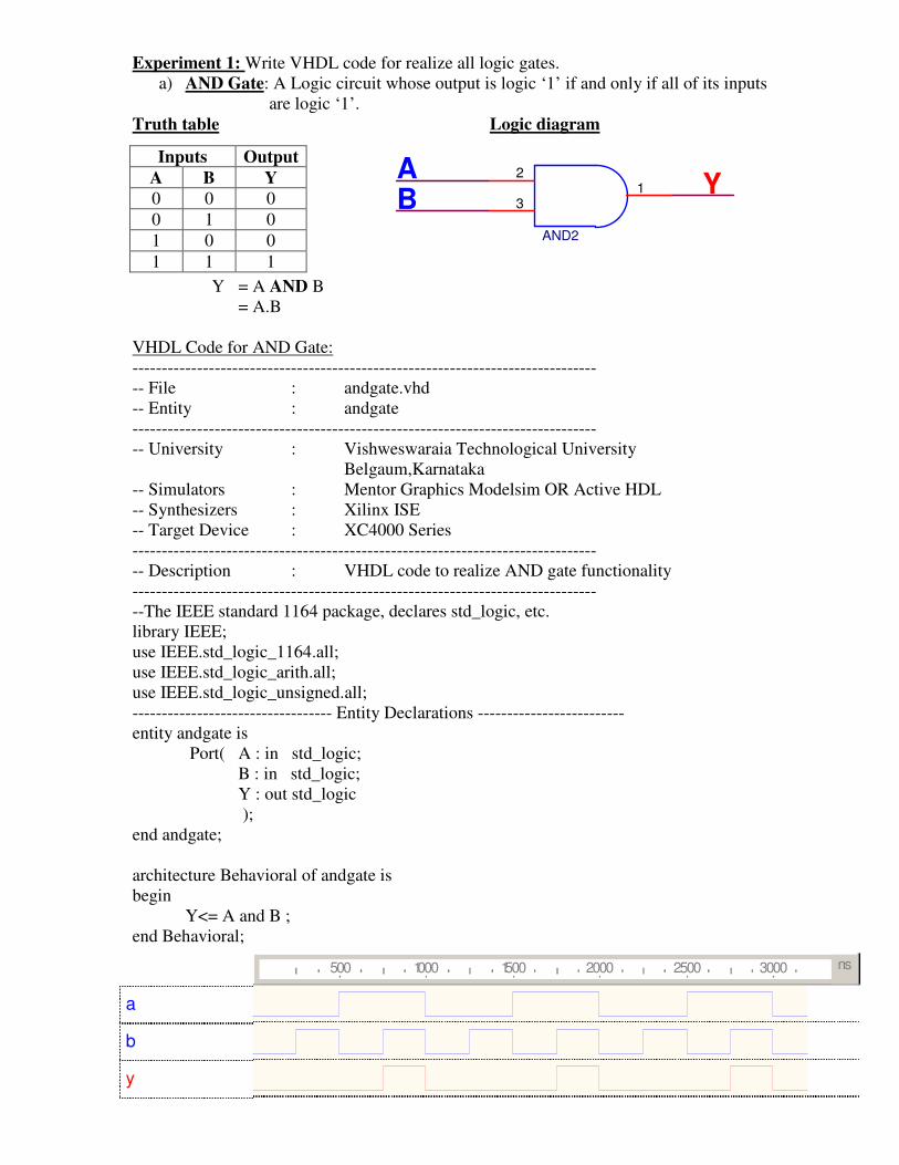
Experiment 1: Write VHDL code for realize all logic gates. a) AND Gate: A Logic circuit whose output is logic ‘1’ if and only if all of its inputs
are logic ‘1’. Truth table Logic diagram
Y = A AND B = A.B VHDL Code for AND Gate: ------------------------------------------------------------------------------- -- File : andgate.vhd -- Entity : andgate ------------------------------------------------------------------------------- -- University : Vishweswaraia Technological University Belgaum,Karnataka -- Simulators : Mentor Graphics Modelsim OR Active HDL -- Synthesizers : Xilinx ISE -- Target Device : XC4000 Series ------------------------------------------------------------------------------- -- Description : VHDL code to realize AND gate functionality ------------------------------------------------------------------------------- --The IEEE standard 1164 package, declares std_logic, etc. library IEEE; use IEEE.std_logic_1164.all; use IEEE.std_logic_arith.all; use IEEE.std_logic_unsigned.all; ---------------------------------- Entity Declarations ------------------------- entity andgate is Port( A : in std_logic; B : in std_logic; Y : out std_logic ); end andgate; architecture Behavioral of andgate is begin Y<= A and B ; end Behavioral;
Inputs Output A B Y 0 0 0 0 1 0 1 0 0 1 1 1
AND2
12
3
A YB
a
b
y
ns500 1000 1500 2000 2500 3000

b)OR Gate: A logic gate whose output is logic ‘0’ if and only if all of its inputs are logic ‘0’.
Truth table Logic diagram
Y = A OR B = A + B VHDL Code for OR Gate: ------------------------------------------------------------------------------- -- File : orgate.vhd -- Entity : orgate ------------------------------------------------------------------------------- -- University : Vishweswaraia Technological University Belgaum,Karnataka -- Simulators : Mentor Graphics Modelsim OR Active HDL -- Synthesizers : Xilinx ISE -- Target Device : XC4000 Series ------------------------------------------------------------------------------- -- Description : VHDL code to realize OR gate functionality ------------------------------------------------------------------------------- --The IEEE standard 1164 package, declares std_logic, etc. library IEEE; use IEEE.std_logic_1164.all; use IEEE.std_logic_arith.all; use IEEE.std_logic_unsigned.all; ---------------------------------- Entity Declarations ------------------------- entity orgate is Port( A : in std_logic; B : in std_logic; Y : out std_logic ); end orgate; architecture Behavioral of orgate is begin Y<= A or B ; end Behavioral;
Inputs Output A B Y 0 0 0 0 1 1 1 0 1 1 1 1
A YBOR2
12
3
a
b
y
500 1000 1500 2000 2500 3000 3500 4000 4500

c) NOT Gate: A logic gate whose input is complement of its input.
Truth table Logic diagram Input Output
A Y 0 1 1 0
Y = NOT A VHDL Code for NOT Gate: ------------------------------------------------------------------------------- -- File : notgate.vhd -- Entity : notgate ------------------------------------------------------------------------------- -- University : Vishweswaraia Technological University Belgaum,Karnataka -- Simulators : Mentor Graphics Modelsim OR Active HDL -- Synthesizers : Xilinx ISE -- Target Device : XC4000 Series ------------------------------------------------------------------------------- -- Description : VHDL code to realize NOT gate functionality ------------------------------------------------------------------------------- --The IEEE standard 1164 package, declares std_logic, etc. library IEEE; use IEEE.std_logic_1164.all; use IEEE.std_logic_arith.all; use IEEE.std_logic_unsigned.all; ---------------------------------- Entity Declarations ------------------------- entity notgate is Port( A : in std_logic; Y : out std_logic ); end notgate; architecture Behavioral of notgate is begin Y<= not A ;
end Behavioral;
YA
INV
a
y
ns500 1000 1500 2000 2500 3000 3500 4000 4500

d) NAND Gate: A logic gate which gives logic ‘0’ output if and only if all of its inputs are logic ‘1’
Truth table Logic diagram
Y= A NAND B =(A. B)\
VHDL Code for NAND Gate: ------------------------------------------------------------------------------- -- File : nandgate.vhd -- Entity : nandgate ------------------------------------------------------------------------------- -- University : Vishweswaraia Technological University Belgaum,Karnataka -- Simulators : Mentor Graphics Modelsim OR Active HDL -- Synthesizers : Xilinx ISE -- Target Device : XC4000 Series ------------------------------------------------------------------------------- -- Description : VHDL code to realize NAND gate functionality ------------------------------------------------------------------------------- --The IEEE standard 1164 package, declares std_logic, etc. library IEEE; use IEEE.std_logic_1164.all; use IEEE.std_logic_arith.all; use IEEE.std_logic_unsigned.all; ---------------------------------- Entity Declarations ------------------------- entity nandgate is Port( A : in std_logic; B : in std_logic; Y : out std_logic ); end nandgate; architecture Behavioral of nandgate is begin Y<= A nand B ;
end Behavioral;
Inputs Output A B Y 0 0 0 0 1 1 1 0 1 1 1 1
BNAND2
12
3
AY
a
b
y
ns500 1000 1500 2000 2500 3000 3500 4000 4500

e) NOR Gate: A logic gate whose output logic ‘1’ if and only if all of its inputs are logic ‘0’
Truth table Logic diagram
Y= A NOR B =(A+ B)\
VHDL Code for NOR Gate: ------------------------------------------------------------------------------- -- File : norgate.vhd -- Entity : norgate ------------------------------------------------------------------------------- -- University : Vishweswaraia Technological University Belgaum,Karnataka -- Simulators : Mentor Graphics Modelsim OR Active HDL -- Synthesizers : Xilinx ISE -- Target Device : XC4000 Series ------------------------------------------------------------------------------- -- Description : VHDL code to realize NOR gate functionality ------------------------------------------------------------------------------- --The IEEE standard 1164 package, declares std_logic, etc. library IEEE; use IEEE.std_logic_1164.all; use IEEE.std_logic_arith.all; use IEEE.std_logic_unsigned.all; ---------------------------------- Entity Declarations ------------------------- entity norgate is Port( A : in std_logic; B : in std_logic; Y : out std_logic ); end norgate; architecture Behavioral of norgate is begin Y<= A nor B ;
end Behavioral;
Inputs Output A B Y 0 0 0 0 1 1 1 0 1 1 1 1
YBNOR2
12
3
A
a
b
y
ns2000 2500 3000 3500 4000

f) EX-OR (Exclusive OR): A logic gate whose output is logic ‘0’ when all the inputs
are equal and logic ‘1’ when they are un equal. Truth table Logic diagram
Y= A EX-OR B = A (+)B = A.B\ + A\.B
VHDL Code for EX-OR Gate: ------------------------------------------------------------------------------- -- File : xorgate.vhd -- Entity : xorgate ------------------------------------------------------------------------------- -- University : Vishweswaraia Technological University Belgaum,Karnataka -- Simulators : Mentor Graphics Modelsim OR Active HDL -- Synthesizers : Xilinx ISE -- Target Device : XC4000 Series ------------------------------------------------------------------------------- -- Description : VHDL code to realize EX-OR gate functionality ------------------------------------------------------------------------------- --The IEEE standard 1164 package, declares std_logic, etc. library IEEE; use IEEE.std_logic_1164.all; use IEEE.std_logic_arith.all; use IEEE.std_logic_unsigned.all; ---------------------------------- Entity Declarations ------------------------- entity xorgate is Port( A : in std_logic; B : in std_logic; Y : out std_logic ); end xorgate; architecture Behavioral of xorgate is begin Y<= A xor B ;
end Behavioral;
Inputs Output A B Y 0 0 0 0 1 1 1 0 1 1 1 0
Y
XOR2
12
3
AB
a
b
y
ns200 400 600 800 1000 1200 1400 1600 1800 2000 2200

g) EX-NOR (Exclusive -NOR) gate: A logic gate that prodices a logic ‘1’ only when
the two inputs are equal Truth table Logic diagram
Y= A XNOR B = (A (+)B)\ = (A.B)\ + A.B
VHDL Code for EX-NOR Gate: ------------------------------------------------------------------------------- -- File : xnorgate.vhd -- Entity : xnorgate ------------------------------------------------------------------------------- -- University : Vishweswaraia Technological University Belgaum,Karnataka -- Simulators : Mentor Graphics Modelsim OR Active HDL -- Synthesizers : Xilinx ISE -- Target Device : XC4000 Series ------------------------------------------------------------------------------- -- Description : VHDL code to realize EX-NOR gate functionality ------------------------------------------------------------------------------- --The IEEE standard 1164 package, declares std_logic, etc. library IEEE; use IEEE.std_logic_1164.all; use IEEE.std_logic_arith.all; use IEEE.std_logic_unsigned.all; ---------------------------------- Entity Declarations ------------------------- entity xnorgate is Port( A : in std_logic; B : in std_logic; Y : out std_logic ); end xnorgate; architecture Behavioral of xnorgate is begin Y<= A xnor B ;
end Behavioral;
Inputs Output A B Y 0 0 0 0 1 1 1 0 1 1 1 0
AB
XNOR2
12
3Y
a
b
y
ns200 400 600 800 1000 1200 1400 1600 1800 2000 2200

Experiment 2: Write a VHDL program for the following combinational designs.
a) 2 to 4 decoder: A decoder is a digital logic circuit that converts n-bits binary input
code in to M output lines. OR It is a logic circuit that decodes from binary to octal, decimal, Hexa-decimal or any other code such as 7-segment etc.
Block Diagram of Decoder
Inputs Output EN Sel(1) Sel(0) D
1 X X 0 0 0 0 D0 0 0 1 D1 0 1 0 D2 0 1 1 D3
Logic Diagram of 2:4 Decoder
Truth table
D3
U6
NAND3
1234
D0
D2
EN
U5
NAND3
1234
SEL(1)
INST1
INV
D1
SEL(0)
INST2
INV
U8
NAND3
1234
U7
NAND3
1234
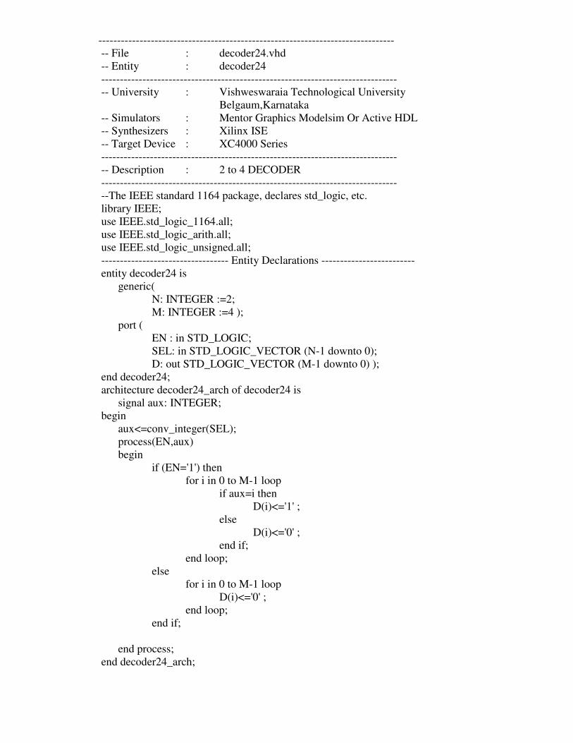
------------------------------------------------------------------------------- -- File : decoder24.vhd -- Entity : decoder24 ------------------------------------------------------------------------------- -- University : Vishweswaraia Technological University Belgaum,Karnataka -- Simulators : Mentor Graphics Modelsim Or Active HDL -- Synthesizers : Xilinx ISE -- Target Device : XC4000 Series ------------------------------------------------------------------------------- -- Description : 2 to 4 DECODER ------------------------------------------------------------------------------- --The IEEE standard 1164 package, declares std_logic, etc. library IEEE; use IEEE.std_logic_1164.all; use IEEE.std_logic_arith.all; use IEEE.std_logic_unsigned.all; ---------------------------------- Entity Declarations ------------------------- entity decoder24 is generic( N: INTEGER :=2; M: INTEGER :=4 ); port ( EN : in STD_LOGIC; SEL: in STD_LOGIC_VECTOR (N-1 downto 0); D: out STD_LOGIC_VECTOR (M-1 downto 0) ); end decoder24; architecture decoder24_arch of decoder24 is signal aux: INTEGER; begin aux<=conv_integer(SEL); process(EN,aux) begin if (EN='1') then for i in 0 to M-1 loop if aux=i then D(i)<='1' ; else D(i)<='0' ; end if; end loop; else for i in 0 to M-1 loop D(i)<='0' ; end loop; end if; end process; end decoder24_arch;

Simulator Waveforms for 2:4 Decoder:
EN
SEL
D
D (3)
D (2)
D (1)
D (0)
n s500 1000 1500 2000 2500
0 1 2 3 0 1 2 3 0 1
0000 0010 0 10 0 10 00 0001 00 10 0 100 1000 0001 0010
2
0100
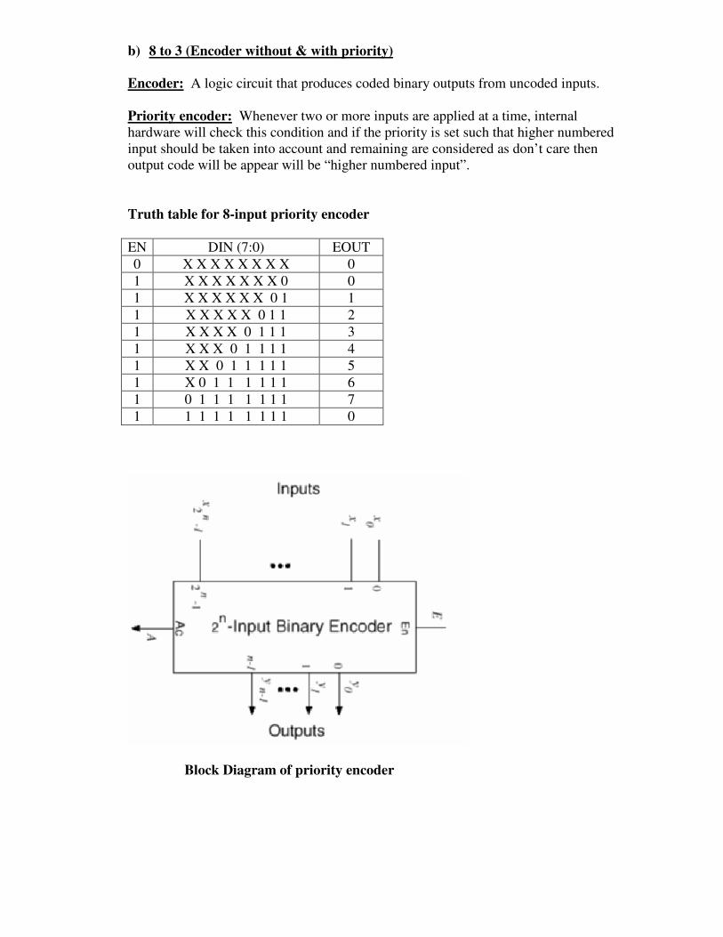
b) 8 to 3 (Encoder without & with priority) Encoder: A logic circuit that produces coded binary outputs from uncoded inputs. Priority encoder: Whenever two or more inputs are applied at a time, internal hardware will check this condition and if the priority is set such that higher numbered input should be taken into account and remaining are considered as don’t care then output code will be appear will be “higher numbered input”. Truth table for 8-input priority encoder EN DIN (7:0) EOUT 0 X X X X X X X X 0 1 X X X X X X X 0 0 1 X X X X X X 0 1 1 1 X X X X X 0 1 1 2 1 X X X X 0 1 1 1 3 1 X X X 0 1 1 1 1 4 1 X X 0 1 1 1 1 1 5 1 X 0 1 1 1 1 1 1 6 1 0 1 1 1 1 1 1 1 7 1 1 1 1 1 1 1 1 1 0
Block Diagram of priority encoder

------------------------------------------------------------------------------- -- File : pencoder.vhd -- Entity : pencoder ------------------------------------------------------------------------------- -- University : Vishweswaraia Technological University Belgaum,Karnataka -- Simulators : Mentor Graphics Modelsim Or Active HDL -- Synthesizers : Xilinx ISE -- Target Device : XC4000 Series ------------------------------------------------------------------------------- -- Description : 8-input priority encoder ------------------------------------------------------------------------------- --The IEEE standard 1164 package, declares std_logic, etc. library IEEE; use IEEE.std_logic_1164.all; use IEEE.std_logic_arith.all; use IEEE.std_logic_unsigned.all; ---------------------------------- Entity Declarations ------------------------- entity pencoder is port ( X: in STD_LOGIC_VECTOR (7 downto 0); E: in STD_LOGIC; Y: out STD_LOGIC_VECTOR (2 downto 0); A: out STD_LOGIC ); end pencoder; architecture pencoder_arch of pencoder is begin pe: process(x,E) variable k: integer; begin y <= "000"; A <= '0'; if E = '1' then for j in 0 to 7 loop if x(j) = '1' then y <= conv_std_logic_vector(j,3); A <= '1'; end if; end loop; end if; end process pe; end pencoder_arch;
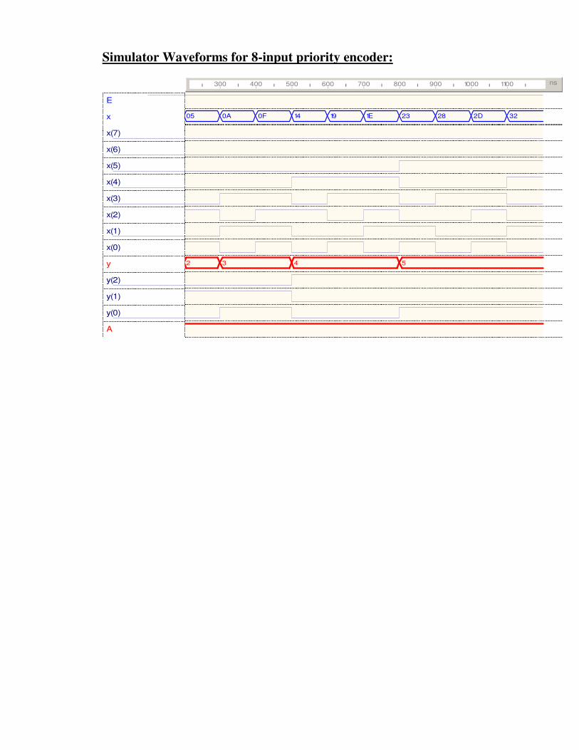
Simulator Waveforms for 8-input priority encoder:
E
x
x(7)
x(6)
x(5)
x(4)
x(3)
x(2)
x(1)
x(0)
y
y(2)
y(1)
y(0)
A
ns300 400 500 600 700 800 900 1000 1100
05 0A 0F 14 19 1E 23 28 2D
2 3 4
32
5

c) 8 :1 Multiplexer: The multiplexer is a combinational circuit which accepts several data inputs and allows only one of them AT A TIME to get through to the output.
Block Diagram of 8:1 Mux Logic Diagram
CONTROL INPUTS EN SEL(3) SEL(3) SEL(3)
OUTPUT(Y) (Selected Inputs)
0 0 0 0 D0 1 0 0 1 D1 1 0 1 0 D2 1 0 1 1 D3 1 1 0 0 D4 1 1 0 1 D5 1 1 1 0 D6 1 1 1 1 D7
EN D0 D1 D2 D3 D4 D5 D6 D7
SEL0 SEL1 SEL2
0 1 2 3 4 5 6 7
O/P
ENABLE
Control Inputs
Data Inputs
Data Output
8:1 Y
U7
AND5
1
23456
SEL(0)
D0
U1
AND5
1
23456
SEL(1)
D7
Y
EN
D3
INV1
D5
U2
AND5
1
23456
U8
AND5
1
23456
U3
AND5
1
23456
U5
AND5
1
23456
U4
AND5
1
23456
INV3
D2
D1
D4
D6
U9
OR8
1
2345
6789
U6
AND5
1
23456
INV2
SEL(2)
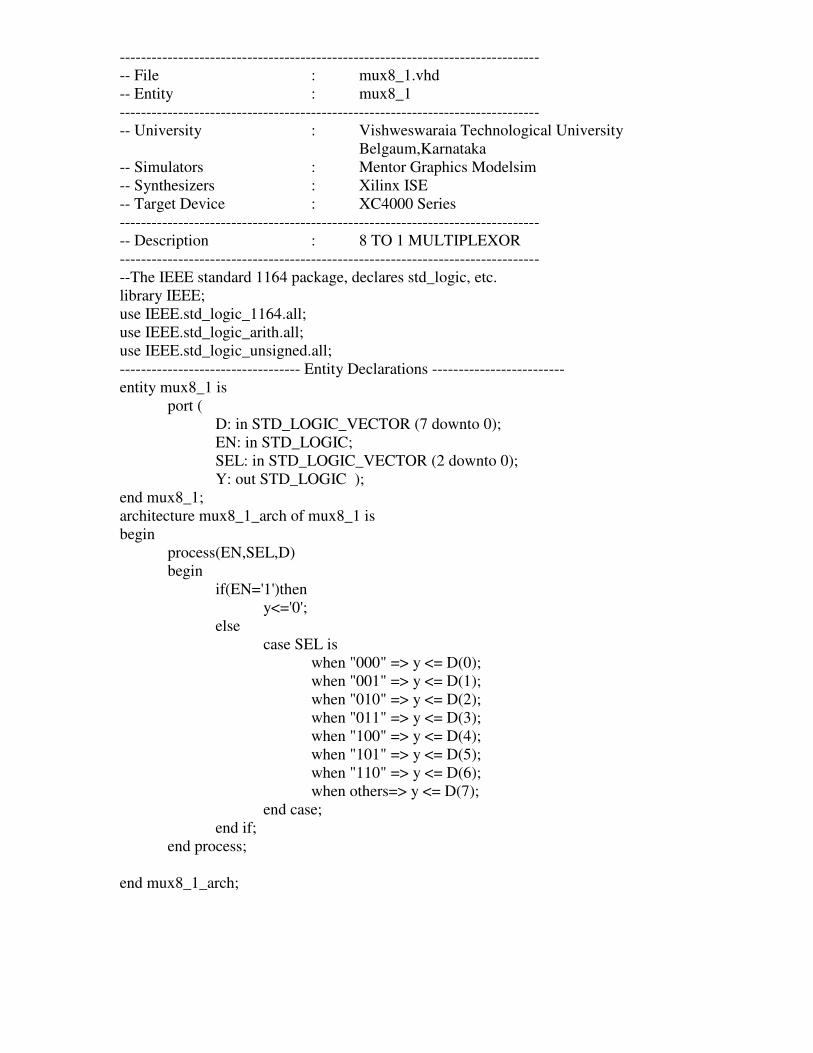
------------------------------------------------------------------------------- -- File : mux8_1.vhd -- Entity : mux8_1 ------------------------------------------------------------------------------- -- University : Vishweswaraia Technological University Belgaum,Karnataka -- Simulators : Mentor Graphics Modelsim -- Synthesizers : Xilinx ISE -- Target Device : XC4000 Series ------------------------------------------------------------------------------- -- Description : 8 TO 1 MULTIPLEXOR ------------------------------------------------------------------------------- --The IEEE standard 1164 package, declares std_logic, etc. library IEEE; use IEEE.std_logic_1164.all; use IEEE.std_logic_arith.all; use IEEE.std_logic_unsigned.all; ---------------------------------- Entity Declarations ------------------------- entity mux8_1 is port ( D: in STD_LOGIC_VECTOR (7 downto 0); EN: in STD_LOGIC; SEL: in STD_LOGIC_VECTOR (2 downto 0); Y: out STD_LOGIC ); end mux8_1; architecture mux8_1_arch of mux8_1 is begin process(EN,SEL,D) begin if(EN='1')then y<='0'; else case SEL is when "000" => y <= D(0); when "001" => y <= D(1); when "010" => y <= D(2); when "011" => y <= D(3); when "100" => y <= D(4); when "101" => y <= D(5); when "110" => y <= D(6); when others=> y <= D(7); end case; end if; end process; end mux8_1_arch;

Simulator Waveforms for 8:1 Multiplexer:
D
D(7)
D(6)
D(5)
D(4)
D(3)
D(2)
D(1)
D(0)
EN
SEL
Y
ns1000 2000 3000 4000 5000 6000 7000 8000 9000
0 1 2 3 4 5 6 7
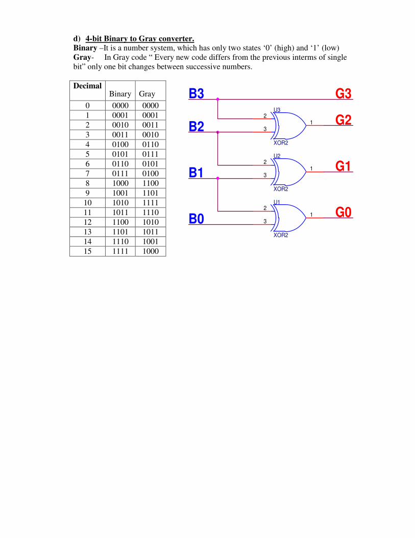
d) 4-bit Binary to Gray converter. Binary –It is a number system, which has only two states ‘0’ (high) and ‘1’ (low) Gray- In Gray code “ Every new code differs from the previous interms of single bit” only one bit changes between successive numbers. Decimal
Binary Gray 0 0000 0000 1 0001 0001 2 0010 0011 3 0011 0010 4 0100 0110 5 0101 0111 6 0110 0101 7 0111 0100 8 1000 1100 9 1001 1101
10 1010 1111 11 1011 1110 12 1100 1010 13 1101 1011 14 1110 1001 15 1111 1000
B0
G3
G0
B2
G1
G2
U2
XOR2
12
3
U1
XOR2
12
3
B1
B3U3
XOR2
12
3

------------------------------------------------------------------------------ -- File :b2g.vhd -- Entity :b2g ------------------------------------------------------------------------------- -- University :Vishweswaraia Technological University Belgaum,Karnataka -- Simulators :Mentor Graphics Modelsim -- Synthesizers :Xilinx ISE -- Target Device :XC4000 Series ------------------------------------------------------------------------------- -- Description : 4-BIT BINARY TO GRAY CONVERTOR ------------------------------------------------------------------------------- --The IEEE standard 1164 package, declares std_logic, etc. library IEEE; use IEEE.std_logic_1164.all; use IEEE.std_logic_arith.all; use IEEE.std_logic_unsigned.all; ---------------------------------- Entity Declarations ------------------------- entity b2g is port ( B3,B2,B1,B0: in STD_LOGIC; G3,G2,G1,G0: out STD_LOGIC ); end b2g; architecture b2g_arch of b2g is begin G3<=B3; G2<=B2 xor B3; G1<=B1 xor B2; G0<=B0 xor B1; end b2g_arch; Simulator Waveforms for 4-Bit Binary to Gray Conversion:
B
G
ns200 400 600 800 1000 1200 1400 1600 1800
0000 0001 0010 0011 0100 0101 0110 0111 1000 1001 1010 1011 1100 1101 1110 1111
0000 0001 0011 0010 0110 0111 0101 0100 1100 1101 1111 1110 1010 1011 1001 1000

e) Multiplexer, Demultiplexer, comparator. Multiplexer: Ref Exp 2(b) Demultiplexer: Demultiplexer is a combinational circuit that accepts single input and distributes it several outputs (Selectively distributes it to 1 of N output channels) & Exhastly reverse of the multiplexer.
Block Diagram of 1:8 Demux Logic Diagram
Truth Table CONTROL INPUTS EN
SEL(3) SEL(3) SEL(3) OUTPUTS
0 X X X 0 1 0 0 0 D0=Y 1 0 0 1 D1=Y 1 0 1 0 D2=Y 1 0 1 1 D3=Y 1 1 0 0 D4=Y 1 1 0 1 D5=Y 1 1 1 0 D6=Y 1 1 1 1 D7=Y
SEL(2)
D7
U5
AND5
1
23456
U4
AND5
1
23456
U2
AND5
1
23456
EN
D4
D5
INV3
SEL(0)
U7
AND5
1
23456
SEL(1)
Y
U3
AND5
1
23456
D6
U1
AND5
1
23456
D0
D1
U6
AND5
1
23456
D2
INV2
D3
INV1
U8
AND5
1
23456
EN
D0
D1
D2
D3
D4
D5
D6
D7
SEL0
SEL1
SEL2
0 1 2 3 4 5 6 7
O/P
ENABLE
Data Input
1:8 Demux
Y
Data Outputs
Control Input

------------------------------------------------------------------------------- -- File : demux.vhd -- Entity : demux ------------------------------------------------------------------------------- -- University : Vishweswaraia Technological University Belgaum,Karnataka -- Simulators : Mentor Graphics Modelsim -- Synthesizers : Xilinx ISE -- Target Device : XC4000 Series ------------------------------------------------------------------------------- -- Description : 1:8 DEMULTIPLEXOR ------------------------------------------------------------------------------- --The IEEE standard 1164 package, declares std_logic, etc. library IEEE; use IEEE.std_logic_1164.all; use IEEE.std_logic_arith.all; use IEEE.std_logic_unsigned.all; ---------------------------------- Entity Declarations ------------------------- entity demux8_1 is port ( Y : in STD_LOGIC; EN : in STD_LOGIC; SEL : in STD_LOGIC_VECTOR (2 downto 0); D : out STD_LOGIC_VECTOR (7 downto 0) ); end demux8_1; architecture demux8_1_arch of demux8_1 is begin process(EN,SEL,Y) begin if(EN='1')then D<=(others=>'0'); else case SEL is when "000" => D(0)<=Y; when "001" => D(1)<=Y; when "010" => D(2)<=Y; when "011" => D(3)<=Y; when "100" => D(4)<=Y; when "101" => D(5)<=Y; when "110" => D(6)<=Y; when others=> D(7)<=Y; end case; end if; end process; end demux8_1_arch;
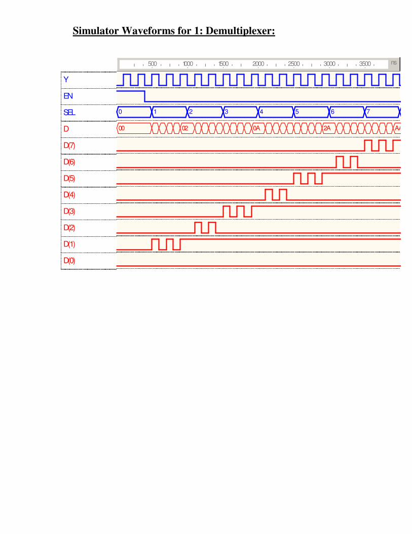
Simulator Waveforms for 1: Demultiplexer:
Y
EN
SEL
D
D(7)
D(6)
D(5)
D(4)
D(3)
D(2)
D(1)
D(0)
ns500 1000 1500 2000 2500 3000 3500
0 1 2 3 4 5 6 7
00 02 0A 2A AA
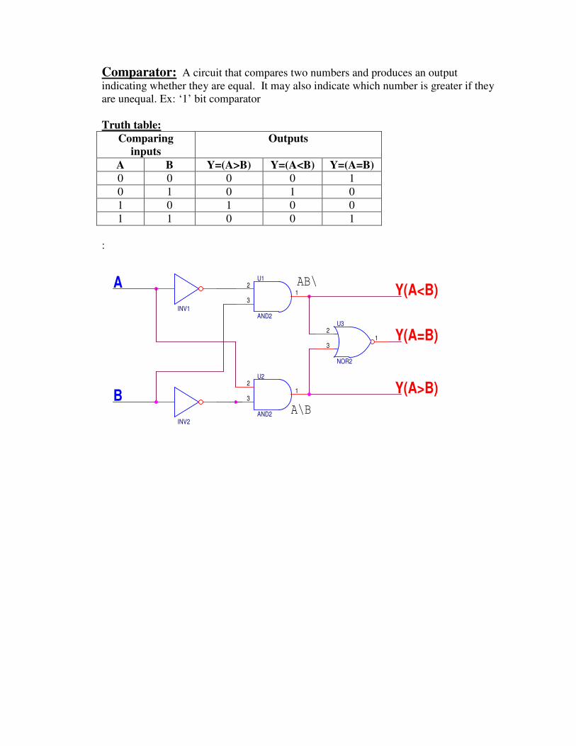
Comparator: A circuit that compares two numbers and produces an output indicating whether they are equal. It may also indicate which number is greater if they are unequal. Ex: ‘1’ bit comparator Truth table:
Comparing inputs
Outputs
A B Y=(A>B) Y=(A<B) Y=(A=B) 0 0 0 0 1 0 1 0 1 0 1 0 1 0 0 1 1 0 0 1
:
INV2
AB\ Y(A<B)INV1
A U1
AND2
12
3
A\B
Y(A>B)U2
AND2
12
3
Y(A=B)
B
U3
NOR2
12
3

------------------------------------------------------------------------------- -- File : bitcomp.vhd -- Entity : bitcomp ------------------------------------------------------------------------------- -- University : Vishweswaraia Technological University Belgaum,Karnataka -- Simulators : Mentor Graphics Modelsim -- Synthesizers : Xilinx ISE -- Target Device : XC4000 Series ------------------------------------------------------------------------------- -- Description : SINGLE BIT MAGNITUDE COMPARATOR. ------------------------------------------------------------------------------- --The IEEE standard 1164 package, declares std_logic, etc. library IEEE; use IEEE.std_logic_1164.all; use IEEE.std_logic_arith.all; use IEEE.std_logic_unsigned.all; ---------------------------------- Entity Declarations ------------------------- entity bitcomp is port ( A: in STD_LOGIC; B: in STD_LOGIC; sel: in STD_LOGIC_VECTOR(1 DOWNTO 0); Y: out BOOLEAN ); end bitcomp; architecture bitcomp_arch of bitcomp is begin process(A,B,sel) begin case sel is when "00" => y <= A=B; when "01" => y <= A>B; when "10" => y <= A<B; when others => y <= FALSE ; end case; end process; end bitcomp_arch;

Simulator Waveforms for SINGLE BIT MAGNITUDE COMPARATOR:
A
B
sel
Y
ns500 1000 1500 2000 2500 3000 3500
0 1 2 3
true false true false true false true false
0
true

Experiment 3: Write a VHDL code to describe the functions of full adder using different modeling styles.
A logic circuit for the addition of two one bit numbers is called half adder (sum and carry are output) and a logic circuit that accepts two one-bit signal and Carry-in as inputs and produces their sum and carry as outputs is called full adder. Truth table for Full adder Truth table for Half adder
INPUTS OUTPUTS A B Cin SUM CARRY 0 0 0 0 0 0 0 1 1 0 0 1 0 1 0 0 1 1 0 1 1 0 0 1 0 1 0 1 0 1 1 1 0 0 1 1 1 1 1 1
Full adder using 2-Half adder
INPUTS OUTPUTS
A B SUM CARRY 0 0 0 0
0 1 1 0
1 0 1 0
1 1 0 1
B
U2
AND2
12
3
A(+)BA(+)B(+)C
CARRYU11
AND2
12
3
A
CARRY
SUM
A.B
A
A.B + B.Cin + A.Cin
U3
AND2
12
3
U10
XOR2
12
3SUM
Cin
U5
OR3
1234
U1
XOR3
1234
B
U4
AND2
12
3
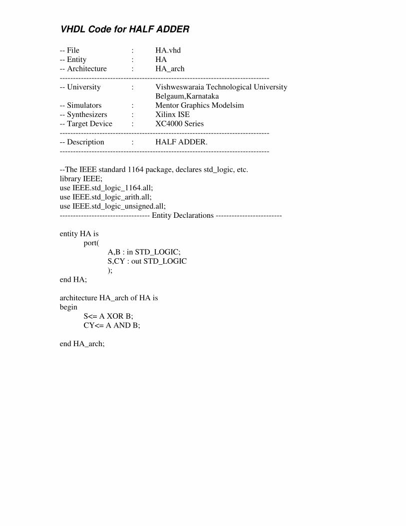
VHDL Code for HALF ADDER -- File : HA.vhd -- Entity : HA -- Architecture : HA_arch ------------------------------------------------------------------------------- -- University : Vishweswaraia Technological University Belgaum,Karnataka -- Simulators : Mentor Graphics Modelsim -- Synthesizers : Xilinx ISE -- Target Device : XC4000 Series ------------------------------------------------------------------------------- -- Description : HALF ADDER. ------------------------------------------------------------------------------- --The IEEE standard 1164 package, declares std_logic, etc. library IEEE; use IEEE.std_logic_1164.all; use IEEE.std_logic_arith.all; use IEEE.std_logic_unsigned.all; ---------------------------------- Entity Declarations ------------------------- entity HA is port( A,B : in STD_LOGIC; S,CY : out STD_LOGIC ); end HA; architecture HA_arch of HA is begin S<= A XOR B; CY<= A AND B; end HA_arch;
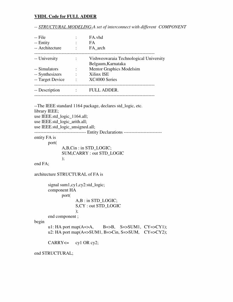
VHDL Code for FULL ADDER -- STRUCTURAL MODELING-A set of interconnect with different COMPONENT -- File : FA.vhd -- Entity : FA -- Architecture : FA_arch ------------------------------------------------------------------------------- -- University : Vishweswaraia Technological University
Belgaum,Karnataka -- Simulators : Mentor Graphics Modelsim -- Synthesizers : Xilinx ISE -- Target Device : XC4000 Series ------------------------------------------------------------------------------- -- Description : FULL ADDER. ------------------------------------------------------------------------------- --The IEEE standard 1164 package, declares std_logic, etc. library IEEE; use IEEE.std_logic_1164.all; use IEEE.std_logic_arith.all; use IEEE.std_logic_unsigned.all; ---------------------------------- Entity Declarations ------------------------- entity FA is port( A,B,Cin : in STD_LOGIC; SUM,CARRY : out STD_LOGIC ); end FA; architecture STRUCTURAL of FA is signal sum1,cy1,cy2:std_logic; component HA port( A,B : in STD_LOGIC; S,CY : out STD_LOGIC ); end component ; begin u1: HA port map(A=>A, B=>B, S=>SUM1, CY=>CY1); u2: HA port map(A=>SUM1, B=>Cin, S=>SUM, CY=>CY2); CARRY<= cy1 OR cy2; end STRUCTURAL;

-- DATAFLOW MODELING-A set of concurrent assignment statements. architecture DATAFLOW of FA is begin SUM<= A XOR B XOR Cin; CARRY<= (A AND B) OR (Cin AND A)OR (Cin AND B); end DATAFLOW; -- BEHAVIORAL MODELING-A set of sequential assignment statements according to -- the behavior of the design. (Process is single concurrent statement, which has sequential statements.) architecture BEHAVIOR of FA is begin process(A,B,Cin) begin SUM<= A XOR B XOR Cin; CARRY<= (A AND B) OR (Cin AND A)OR (Cin AND B); end process; end BEHAVIOR;

Simulator waveforms of HALF ADDER Simulator waveforms of FULL ADDER
A
B
SUM
CARRY
us1 2 3 4 5 6 7 8 9
A
B
Cin
SUM
CARRY
ns100 200 300 400 500 600 700 800 900

Experiment 4: Write a model for 32 bit ALU using the schematic diagram Shown below example
� ALU should use the combinational logic to calculate an output based on the four bit Opcode input.
� ALU should pass the result to the out bit when enable line is high and tri-state when low enable.
� ALU should decode the 4-bit op-code according to the given in example below Opcode ALU operation
1 A + B 2 A – B 3 A Complement 4 A * B 5 A AND B 6 A OR B 7 A NAND B 8 A XOR B
Function table for ALU Enable Mode Opcode Functional description
0 X XXXX Y<=”Z” (Tri-stated) 1 0 0001 Y<= A + B ; 1 0 0010 Y<= A – B; 1 0 0011 Y <= A(15:0)* B(15:0)* ; 1 1 0100 Y <= NOT A (Complement) 1 1 0101 Y <= A AND B (AND Operation) 1 1 0110 Y <= A OR B (OR Operation) 1 1 0111 Y <= A NAND B (NAND Operation) 1 1 1000 Y <= A XOR B (XOR Operation) 1 X 1001 Y <= Y (ALU is ideal or previous data is
latched for all other higher opcodes. 1 X 10¹⁰ “ “ 1 X 10¹¹ “ “ 1 X 1100 “ “ 1 X 1101 “ “ 1 X 1110 “ “ 1 X 1111 “ “

ARTHAMETIC LOGIC UNIT (ALU) ALU is logic circuit which is able to perform different arithmetic and logical function basically ALU is the heart of central processing unit (CPU).
Opcode [3:0]
Mode Mode : ‘0’____ Arthmatic operation ‘1’____Logic operation Enable ‘0’ Y <= “ Z “ ‘1’ Out put performed Note: For A*B, A&B lower 16 bit [15:0] can be taken in to consideration.
One stage of Arithmetic circuit
One stage of Logic circuit
2:1 Mux
0
1 32
32 4
32 32
Enable
A B
Cin Cin + 1 (CY)
0
1 32 Y
(Data o/p)
Data i/p
Control Signals
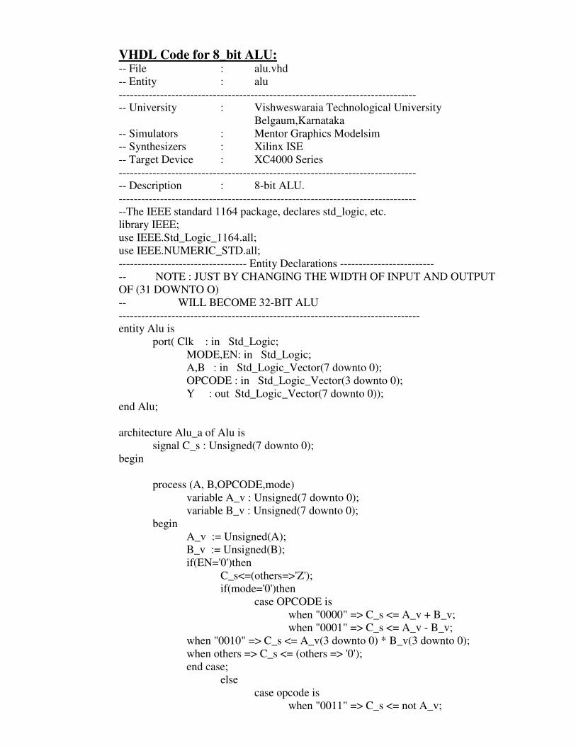
VHDL Code for 8_bit ALU: -- File : alu.vhd -- Entity : alu ------------------------------------------------------------------------------- -- University : Vishweswaraia Technological University Belgaum,Karnataka -- Simulators : Mentor Graphics Modelsim -- Synthesizers : Xilinx ISE -- Target Device : XC4000 Series ------------------------------------------------------------------------------- -- Description : 8-bit ALU. ------------------------------------------------------------------------------- --The IEEE standard 1164 package, declares std_logic, etc. library IEEE; use IEEE.Std_Logic_1164.all; use IEEE.NUMERIC_STD.all; ---------------------------------- Entity Declarations ------------------------- -- NOTE : JUST BY CHANGING THE WIDTH OF INPUT AND OUTPUT OF (31 DOWNTO O) -- WILL BECOME 32-BIT ALU -------------------------------------------------------------------------------- entity Alu is port( Clk : in Std_Logic; MODE,EN: in Std_Logic; A,B : in Std_Logic_Vector(7 downto 0); OPCODE : in Std_Logic_Vector(3 downto 0); Y : out Std_Logic_Vector(7 downto 0)); end Alu; architecture Alu_a of Alu is signal C_s : Unsigned(7 downto 0); begin process (A, B,OPCODE,mode) variable A_v : Unsigned(7 downto 0); variable B_v : Unsigned(7 downto 0); begin A_v := Unsigned(A); B_v := Unsigned(B); if(EN='0')then C_s<=(others=>'Z'); if(mode='0')then case OPCODE is when "0000" => C_s <= A_v + B_v; when "0001" => C_s <= A_v - B_v; when "0010" => C_s <= A_v(3 downto 0) * B_v(3 downto 0); when others => C_s <= (others => '0'); end case; else case opcode is when "0011" => C_s <= not A_v;

when "0100" => C_s <= not B_v; when "0101" => C_s <= A_v and B_v; when "0110" => C_s <= A_v nand B_v; when "0111" => C_s <= A_v or B_v; when "1000" => C_s <= A_v nor B_v; when "1001" => C_s <= A_v xor B_v; when "1010" => C_s <= A_v xnor B_v; when others => C_s <= (others => '0'); end case; end if; end if; end process; process begin wait until Clk'event and Clk = '1'; y <= Std_Logic_Vector(C_s); end process ; end Alu_a; Simulator waveforms for 8_bit ALU:
Clk
MODE
EN
A
B
OPCODE
Y
ns50 100 150 200 250 300 350
0 1 2 3 4 3 4 5 6 7 8 9 A B C
UU 04 20 00 F7 FB 00 FF 0C F3 0C F3
08
04
D
00

Experiment 5: Develop the VHDL code for the following flip-flops SR, D, JK & T.
Flip-flop: Flip-flop is a sequential logic circuit, which is ‘One ‘-bit memory element. OR It is a basic memory element in digital systems (same as the bi-stable multivibrator) It has two stable state logic ‘1’ and logic ‘0’.
(a) S-R Flip-flop (Set-Reset) In a memory device set and Reset is often required for synchronization of the device in such case S-R Flip-flop is need & this is refereed as clocked set-reset.
�Set-Reset Truth table
? Q Clk ? Q\
o
o
Set
Rst
? Q Clk ? Q\
o
Set
Rst
Positive Edge-Triggered Negative Edge-Triggered
Illegal - 1 1
Set 1 0 1
Reset 0 1 0
No Change
Q 0 0
Action Q+ R S

VHDL Code for SR Flip-Flop: ------------------------------------------------------------------------------- -- File : SRFF.vhd -- Entity : SRFF ------------------------------------------------------------------------------- -- University : Vishweswaraia Technological University Belgaum,Karnataka -- Simulators : Mentor Graphics Modelsim Or Active HDL -- Synthesizers : Xilinx ISE -- Target Device : XC4000 Series ------------------------------------------------------------------------------- -- Description : SR Flip-Flop ------------------------------------------------------------------------------- --The IEEE standard 1164 package, declares std_logic, etc. library IEEE; use IEEE.std_logic_1164.all; use IEEE.std_logic_arith.all; use IEEE.std_logic_unsigned.all; ---------------------------------- Entity Declarations ------------------------- entity SRFF is port ( CLK, RST, S, R : in std_logic; Q, Qn : out std_logic); end SRFF; architecture RTL of SRFF is signal FF : std_logic; begin process (CLK, RST) variable SR : std_logic_vector(1 downto 0); begin if (RST = '0') then FF <= '0'; elsif (CLK'event and CLK = '1') then SR := S & R; case SR is when "01" => FF <= '0'; when "10" => FF <= '1'; when "11" => FF <= 'Z'; when others => FF <= FF; end case; end if; end process; Q <= FF ; Qn <= not FF ; end RTL;
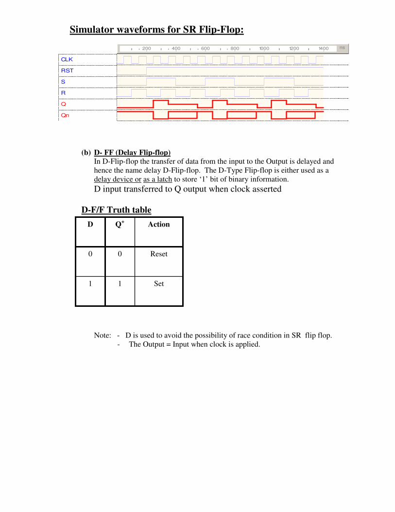
Simulator waveforms for SR Flip-Flop:
CLK
RST
S
R
Q
Qn
ns200 400 600 800 1000 1200 1400
(b) D- FF (Delay Flip-flop)
In D-Flip-flop the transfer of data from the input to the Output is delayed and hence the name delay D-Flip-flop. The D-Type Flip-flop is either used as a delay device or as a latch to store ‘1’ bit of binary information. D input transferred to Q output when clock asserted
D-F/F Truth table
Note: - D is used to avoid the possibility of race condition in SR flip flop.
- The Output = Input when clock is applied.
Set 1 1
Reset 0 0
Action Q+ D
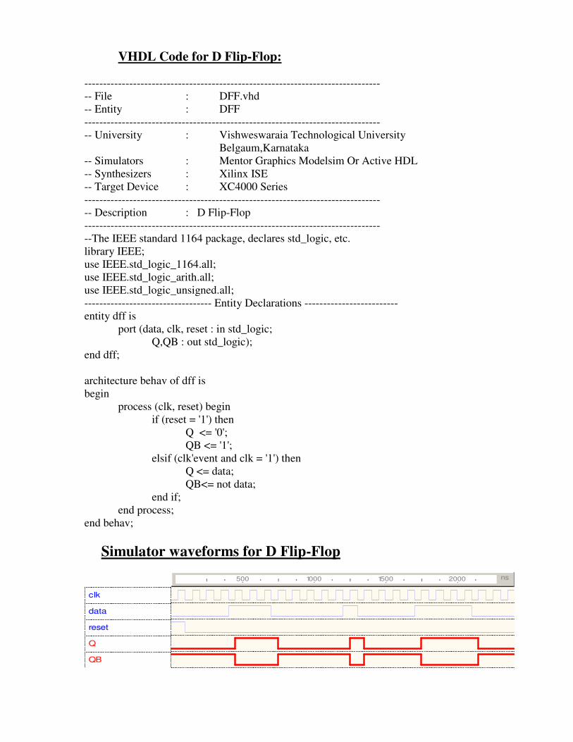
VHDL Code for D Flip-Flop:
------------------------------------------------------------------------------- -- File : DFF.vhd -- Entity : DFF ------------------------------------------------------------------------------- -- University : Vishweswaraia Technological University Belgaum,Karnataka -- Simulators : Mentor Graphics Modelsim Or Active HDL -- Synthesizers : Xilinx ISE -- Target Device : XC4000 Series ------------------------------------------------------------------------------- -- Description : D Flip-Flop ------------------------------------------------------------------------------- --The IEEE standard 1164 package, declares std_logic, etc. library IEEE; use IEEE.std_logic_1164.all; use IEEE.std_logic_arith.all; use IEEE.std_logic_unsigned.all; ---------------------------------- Entity Declarations ------------------------- entity dff is port (data, clk, reset : in std_logic; Q,QB : out std_logic); end dff; architecture behav of dff is begin process (clk, reset) begin if (reset = '1') then Q <= '0'; QB <= '1'; elsif (clk'event and clk = '1') then Q <= data; QB<= not data; end if; end process; end behav;
Simulator waveforms for D Flip-Flop
clk
data
reset
Q
QB
ns500 1000 1500 2000

c) J.K Flip-flop: The race conditions in S-R Flip-flop can be eliminated by converting it in to J.K, the data inputs J and K are ANDed with Q\ and Q to obtain S & R inputs. Here SR, T, or D depending on inputs. S=J.Q\ R=K.Q Logic diagram:
JK-F/F Truth table
VHDL Code for JK Flip-Flop: -------------------------------------------------------------------------------
-- File : JKFF.vhd -- Entity : JKFF ------------------------------------------------------------------------------- -- University : Vishweswaraia Technological University Belgaum,Karnataka -- Simulators : Mentor Graphics Modelsim Or Active HDL -- Synthesizers : Xilinx ISE -- Target Device : XC4000 Series ------------------------------------------------------------------------------- -- Description :JK Flip-Flop ------------------------------------------------------------------------------- --The IEEE standard 1164 package, declares std_logic, etc. library IEEE; use IEEE.std_logic_1164.all; use IEEE.std_logic_arith.all; use IEEE.std_logic_unsigned.all; ---------------------------------- Entity Declarations ------------------------- entity JKFF is port ( CLK, RST, J, K : in std_logic; Q, Qn : out std_logic); end JKFF; architecture RTL of JKFF is
Toggle Q 1 1
Set 1 0 1
Reset 0 1 0
No Change Q 0 0
Action Q+ K J
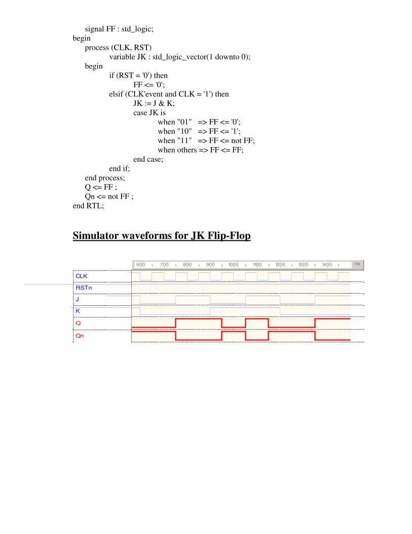
signal FF : std_logic; begin process (CLK, RST) variable JK : std_logic_vector(1 downto 0); begin if (RST = '0') then FF <= '0'; elsif (CLK'event and CLK = '1') then JK := J & K; case JK is when "01" => FF <= '0'; when "10" => FF <= '1'; when "11" => FF <= not FF; when others => FF <= FF; end case; end if; end process; Q <= FF ; Qn <= not FF ; end RTL; Simulator waveforms for JK Flip-Flop
CLK
RSTn
J
K
Q
Qn
ns600 700 800 900 1000 1100 1200 1300 1400

d) T-Flip-flop (Toggle Flip-flop): On every change in clock pulse the output ‘Q’ changes its state (Toggle). A Flip-flop with one data input which changes state for every clock pulse.(J=K=’1’ in JQK Flip-flop the resulting output is ‘T’ Flip-flop).
T-F/F Truth table VHDL Code for T Flip-Flop: ------------------------------------------------------------------------------ -- File : TFF.vhd -- Entity : TFF ------------------------------------------------------------------------------- -- University : Vishweswaraia Technological University Belgaum,Karnataka -- Simulators : Mentor Graphics Modelsim Or Active HDL -- Synthesizers : Xilinx ISE -- Target Device : XC4000 Series ------------------------------------------------------------------------------- -- Description : T Flip-Flop ------------------------------------------------------------------------------- --The IEEE standard 1164 package, declares std_logic, etc. library IEEE; use IEEE.std_logic_1164.all; use IEEE.std_logic_arith.all; use IEEE.std_logic_unsigned.all; ---------------------------------- Entity Declarations ------------------------- entity tff is port (T, CLK, RST : in std_logic; Q,QB : out std_logic); end tff; architecture behav of tff is begin process (clk, RST) begin if (RST = '1') then Q <= '1'; QB <= '0'; elsif (clk'event and clk = '1') then QB <= T; Q <= not T; end if; end process; end behav;
Toggle Q 1
No Change Q 0
Action Q+
T

Simulator waveforms for D Flip-Flop:
T
CLK
RST
Q
QB
ns200 400 600 800 1000 1200
Gate level Example:
U3
NAND2
12
3 Q
U6
AND2
12
3
U2
NAND2
12
3
C1CLK
U4
NAND2
12
3
R2R1
J
Q\
+Ve edge triggerd JK Flip-flop
R
INST1
INV
U1
NAND2
12
3
S
K
U5
AND2
12
3

Experiment 6: Design 4-bit binary, BCD counters and any sequence counter
(With Synchronous /Asynchronous Reset). COUNTER: Counter is a digital circuit that can counts the member of pulse for building the counters, Flip-flop are used. Relation between number of Flip-flop used and number of state of counter is (Regular/binary counter).
Ripple Counter/Asynchronous Counter:
Synchronous Counter:

4-bit Binary counter (Synchronous counter) ------------------------------------------------------------------------------- -- File : sync_rst_binary.vhd -- Entity : sync_rst_binary -- Architecture : sync_rst_binary_arch ------------------------------------------------------------------------------- -- University : Vishweswaraia Technological University Belgaum,Karnataka -- Simulators : Mentor Graphics Modelsim Or Active HDL -- Synthesizers : Xilinx ISE -- Target Device : XC4000 Series ------------------------------------------------------------------------------- -- Description : N-bit binary Up counter with synchronous reset ------------------------------------------------------------------------------- --The IEEE standard 1164 package, declares std_logic, etc. library IEEE; use IEEE.std_logic_1164.all; use IEEE.std_logic_arith.all; use IEEE.std_logic_unsigned.all; ---------------------------------- Entity Declarations ------------------------- entity sync_rst_binary is generic(N: INTEGER := 4); port( clock : in STD_LOGIC; reset : in STD_LOGIC; qout : out STD_LOGIC_VECTOR(N-1 downto 0) ); end sync_rst_binary; architecture sync_rst_binary_arch of sync_rst_binary is signal temp_count: std_logic_vector(N-1 downto 0); begin process(clock,reset) begin if(clock='1' and clock'event)then if(reset='1')then temp_count<=(others=>'0'); else temp_count<= temp_count + 1; end if; end if; end process; qout<=temp_count; end sync_rst_binary_arch;

4-bit Binary up counter (Asynchronous counter) ------------------------------------------------------------------------------- -- File : async_rst_binary.vhd -- Entity : async_rst_binary -- Architecture : async_rst_binary_arch ------------------------------------------------------------------------------- -- University : Vishweswaraia Technological University Belgaum,Karnataka -- Simulators : Mentor Graphics Modelsim Or Active HDL -- Synthesizers : Xilinx ISE -- Target Device : XC4000 Series ------------------------------------------------------------------------------- -- Description : N-bit binary Up counter with Asynchronous reset ------------------------------------------------------------------------------- --The IEEE standard 1164 package, declares std_logic, etc. library IEEE; use IEEE.std_logic_1164.all; use IEEE.std_logic_arith.all; use IEEE.std_logic_unsigned.all; ---------------------------------- Entity Declarations ------------------------- entity async_rst_binary is generic(N: INTEGER := 4); port( clock : in STD_LOGIC; reset : in STD_LOGIC; qout : out STD_LOGIC_VECTOR(N-1 downto 0) ); end async_rst_binary; architecture async_rst_binary_arch of async_rst_binary is signal temp_count: std_logic_vector(N-1 downto 0); begin process(clock,reset) begin if(reset='1')then temp_count<=(others=>'0'); elsif(clock='1' and clock'event)then temp_count<= temp_count + 1; end if; end process; qout<=temp_count; end async_rst_binary_arch;

4-bit BCD up counter (Synchronous counter) ------------------------------------------------------------------------------- -- File : sync_rst_BCD.vhd -- Entity : sync_rst_BCD -- Architecture : sync_rst_BCD_arch ------------------------------------------------------------------------------- -- University : Vishweswaraia Technological University
Belgaum,Karnataka -- Simulators : Mentor Graphics Modelsim Or Active HDL -- Synthesizers : Xilinx ISE -- Target Device : XC4000 Series ------------------------------------------------------------------------------- -- Description : N-bit BCD UP counter with Synchronous reset ------------------------------------------------------------------------------- --The IEEE standard 1164 package, declares std_logic, etc. library IEEE; use IEEE.std_logic_1164.all; use IEEE.std_logic_arith.all; use IEEE.std_logic_unsigned.all; ---------------------------------- Entity Declarations ------------------------- entity sync_rst_BCD4 is generic(N: INTEGER := 4); port( clock : in STD_LOGIC; reset : in STD_LOGIC; qout : out STD_LOGIC_VECTOR(N-1 downto 0) ); end sync_rst_BCD4; architecture sync_rst_BCD4_arch of sync_rst_BCD4 is signal temp_count: std_logic_vector(N-1 downto 0); begin process(clock,reset) begin if (clock='1' and clock'event)then if(reset='1')then temp_count<=(others=>'0'); else temp_count<= temp_count + 1; if(temp_count="1001")then temp_count<=(others=>'0'); end if; end if; end if; end process; qout<=temp_count; end sync_rst_BCD4_arch;

4-bit BCD up counter (Asynchronous Reset) ------------------------------------------------------------------------------- -- File : async_rst_BCD.vhd -- Entity : async_rst_BCD -- Architecture : async_rst_BCD_arch ------------------------------------------------------------------------------- -- University : Vishweswaraia Technological University
Belgaum,Karnataka -- Simulators : Mentor Graphics Modelsim Or Active HDL -- Synthesizers : Xilinx ISE -- Target Device : XC4000 Series ------------------------------------------------------------------------------- -- Description : N-bit BCD UP counter with Aynchronous reset ------------------------------------------------------------------------------- --The IEEE standard 1164 package, declares std_logic, etc. library IEEE; use IEEE.std_logic_1164.all; use IEEE.std_logic_arith.all; use IEEE.std_logic_unsigned.all; ---------------------------------- Entity Declarations ------------------------- entity async_rst_BCD4 is generic(N: INTEGER := 4); port( clock : in STD_LOGIC; reset : in STD_LOGIC; qout : out STD_LOGIC_VECTOR(N-1 downto 0) ); end async_rst_BCD4; architecture async_rst_BCD4_arch of async_rst_BCD4 is signal temp_count: std_logic_vector(N-1 downto 0); begin process(clock,reset) begin if(reset='1')then temp_count<=(others=>'0'); elsif(clock='1' and clock'event)then temp_count<= temp_count + 1; if(temp_count="1001")then temp_count<=(others=>'0'); end if; end if; end process; qout<=temp_count; end async_rst_BCD4_arch;

4-bit Gray up counter (Asynchronous Reset) ------------------------------------------------------------------------------- -- File : graycnt.vhd -- Entity : graycnt -- Architecture : graycnt_arch ------------------------------------------------------------------------------- -- University : Vishweswaraia Technological University
Belgaum,Karnataka -- Simulators : Mentor Graphics Modelsim Or Active HDL -- Synthesizers : Xilinx ISE -- Target Device : XC4000 Series ------------------------------------------------------------------------------- -- Description : N-bit Gary up counter with Asynchronous reset ------------------------------------------------------------------------------- --The IEEE standard 1164 package, declares std_logic, etc. library IEEE; use IEEE.std_logic_1164.all; use IEEE.std_logic_arith.all; use IEEE.std_logic_unsigned.all; ---------------------------------- Entity Declarations ------------------------- entity graycnt is generic(N: INTEGER := 4); port( clock : in STD_LOGIC; reset : in STD_LOGIC; grayout,binaryout : out std_logic_vector(N-1 downto 0) ); end graycnt; architecture graycnt of graycnt is signal temp_count: std_logic_vector(N-1 downto 0); begin process(clock,reset) begin if(reset='1')then temp_count<=(others=>'0'); elsif(clock='1' and clock'event)then temp_count<= temp_count + 1; end if; end process; binaryout<=temp_count; grayout(3)<=temp_count(3); grayout(2)<=temp_count(3)xor temp_count(2); grayout(1)<=temp_count(2)xor temp_count(1); grayout(0)<=temp_count(1)xor temp_count(0); end graycnt;

Waveforms for 4-Bit Binary Up Counter Waveforms for 4-Bit BCD Up Counter
Waveforms for 4-Bit Gray Counter
clock
reset
qout
qout(3)
qout(2)
qout(1)
qout(0)
ns200 400 600 800 1000 1200 1400 1600 1800 2000
0 1 2 3 4 5 6 7 8 9 A B C D E F 0 1 2 3 4
clock
reset
qout
qout(3)
qout(2)
qout(1)
qout(0)
ns400 600 800 1000 1200 1400 1600 1800 2000
1 2 3 4 5 6 7 8 9 0 1 2 3 4 5 6 7 8 9
clock
reset
binaryout
grayout
ns200 400 600 800 1000 1200 1400
0000 0001 0011 0010 0110 0111 0101 0100 1100 1101 1111 1110 1010 1011 1001 1000
0000 0001 0010 0011 0100 0101 0110 0111 1000 1001 1010 1011 1100 1101 1110 1111
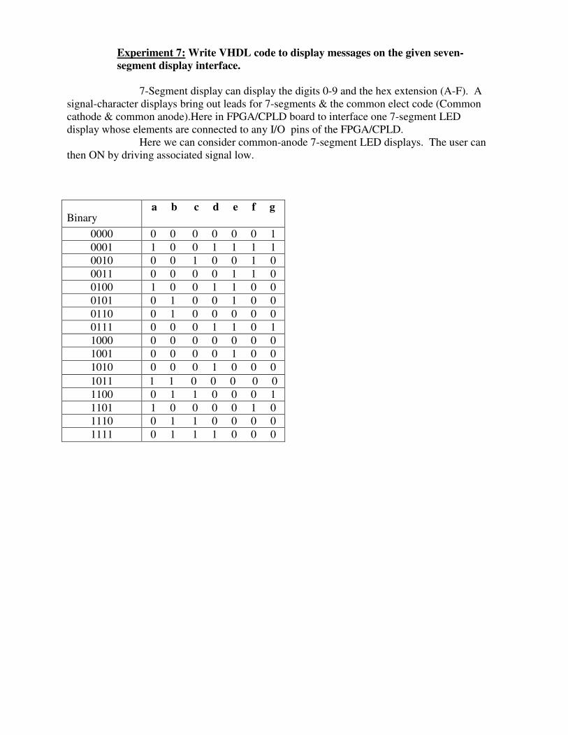
Experiment 7: Write VHDL code to display messages on the given seven-segment display interface.
7-Segment display can display the digits 0-9 and the hex extension (A-F). A signal-character displays bring out leads for 7-segments & the common elect code (Common cathode & common anode).Here in FPGA/CPLD board to interface one 7-segment LED display whose elements are connected to any I/O pins of the FPGA/CPLD. Here we can consider common-anode 7-segment LED displays. The user can then ON by driving associated signal low.
Binary a b c d e f g
0000 0 0 0 0 0 0 1 0001 1 0 0 1 1 1 1 0010 0 0 1 0 0 1 0 0011 0 0 0 0 1 1 0 0100 1 0 0 1 1 0 0 0101 0 1 0 0 1 0 0 0110 0 1 0 0 0 0 0 0111 0 0 0 1 1 0 1 1000 0 0 0 0 0 0 0 1001 0 0 0 0 1 0 0 1010 0 0 0 1 0 0 0 1011 1 1 0 0 0 0 0 1100 0 1 1 0 0 0 1 1101 1 0 0 0 0 1 0 1110 0 1 1 0 0 0 0 1111 0 1 1 1 0 0 0

Interfacing Diagram:
(a) LED segments (b) Four displays with common anode and (c) LED connection on CPLD or FPGA Board. Turning on an LED: (For +5V) Note: If your Seven-segment LED is having Digit point, Then turn on with giving Logic ‘1’ to dig.pt permanently when particular Seven-segment is enabled.
+5V R LED
GAL output pin
+5V R LED
GAL output pin
1
0
+5V
+0.2V +1.7V
No current
Current light
no light
R = voltage current =
5 - 1.7 15 x 10 -3
= 220 ohms
Common Anode
+3.3V/
+3.3V/
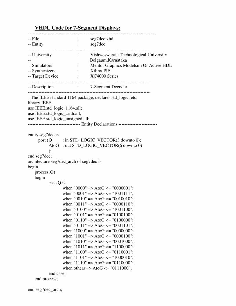
VHDL Code for 7-Segment Displays: ---------------------------------------------------------------------------------- -- File : seg7dec.vhd -- Entity : seg7dec ------------------------------------------------------------------------------- -- University : Vishweswaraia Technological University -- Belgaum,Karnataka -- Simulators : Mentor Graphics Modelsim Or Active HDL -- Synthesizers : Xilinx ISE -- Target Device : XC4000 Series ------------------------------------------------------------------------------- -- Description : 7-Segment Decoder ------------------------------------------------------------------------------- --The IEEE standard 1164 package, declares std_logic, etc. library IEEE; use IEEE.std_logic_1164.all; use IEEE.std_logic_arith.all; use IEEE.std_logic_unsigned.all; ---------------------------------- Entity Declarations ------------------------- entity seg7dec is port ( Q : in STD_LOGIC_VECTOR(3 downto 0); AtoG : out STD_LOGIC_VECTOR(6 downto 0)
); end seg7dec; architecture seg7dec_arch of seg7dec is begin process(Q) begin case Q is when "0000" => AtoG <= "0000001"; when "0001" => AtoG <= "1001111"; when "0010" => AtoG <= "0010010"; when "0011" => AtoG <= "0000110"; when "0100" => AtoG <= "1001100"; when "0101" => AtoG <= "0100100"; when "0110" => AtoG <= "0100000"; when "0111" => AtoG <= "0001101"; when "1000" => AtoG <= "0000000"; when "1001" => AtoG <= "0000100"; when "1010" => AtoG <= "0001000"; when "1011" => AtoG <= "1100000"; when "1100" => AtoG <= "0110001"; when "1101" => AtoG <= "1000010"; when "1110" => AtoG <= "0110000"; when others => AtoG <= "0111000"; end case; end process; end seg7dec_arch;
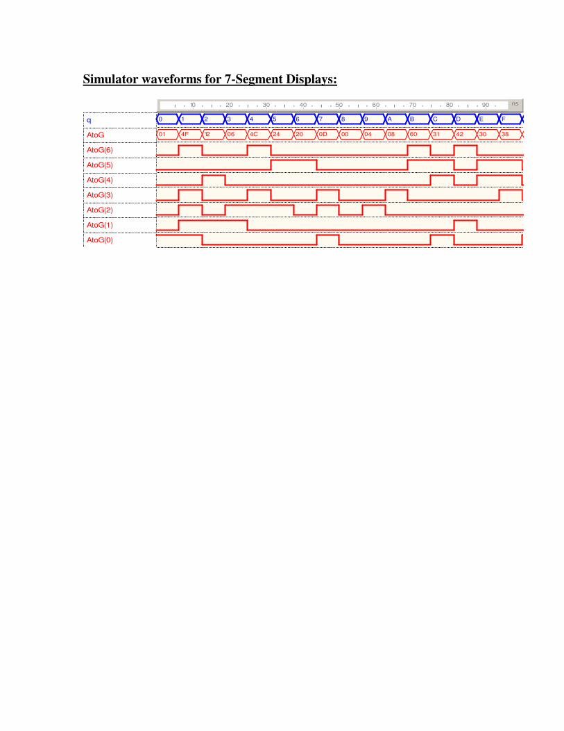
Simulator waveforms for 7-Segment Displays:
q
AtoG
AtoG(6)
AtoG(5)
AtoG(4)
AtoG(3)
AtoG(2)
AtoG(1)
AtoG(0)
ns10 20 30 40 50 60 70 80 90
0 1 2 3 4 5 6 7 8 9 A B C D E F
01 4F 12 06 4C 24 20 0D 00 04 08 60 31 42 30 38

Experiment 8: Write a VHDL codes to display messages on given LCD panel.
The LCD should be initialize before displaying any characters, the initialization procedures for my LCD driver are:
1. Function set - set 8 bit long data interface 2. Display on - set display on, cursor on, and blink on. 3. Entry mode set - set entry mode to increment the cursor after a character is displayed. 4. Display Clear - clear the LCD display. Important things about LCD timings are: 1. The LCD should have at least 1.64ms to process clear or home instruction and 40us to process any other instructions. 2. When the register select signal is changed, there should be a 140ns address setup time before the enable signal is set to 1. 3. When displaying char. on the LCD, enable signal should have be 1 for at least 450ns. 4. The data setup time and data hold time should be at least 195ns and 10ns respectively.
The ASCII representations of each individual character are being entered into the program and displayed on to the LCD screen
LCD Interface circuit Diagram:
R1
POT
13
2
VCC0.1 uF
C
CPLD/FPGA
7-14
D0-D7
I/O RS I/O R/W I/O EN I/Os
4 5 6 7-14
2 VDD 3 V0 1 VSS
LCD 20*4
+5V/3.3V

Pin out of LCD and Description of each pins:
Pin No.
Signal Name Input/Output Function
1 VSS Input Ground
2 VDD Input +5V
3 VEE Input Contrast Adjust
4 RS Input
Signal to select registers '0' : instruction register (for write) Busy flag : address counter (for read) '1' : Data register (for read and write)
5 R/W InputSignal to select read (R) and write (W) '0' : Write '1' : Read
6 Enable Input Operation start signal for data read/write
7-14 DB0-DB7 Input/Output8 bit bidirectional three-state data bus lines. Used for data transfer between FPGA and LCD
Instructions for Initialization of LCD:
Instruction RS R/W DB7 DB6 DB5 DB4 DB3 DB2 DB1 DB0 Description Execution Time (Max)
Clear Display 0 0 0 0 0 0 0 0 0 1
Clear entire display and sets DD RAM address 0 in address counter.
1.64 ms
Return Home 0 0 0 0 0 0 0 0 1 X
Sets DD RAM address 0 in address counter. Also returns display being shifted to original position. DD RAM contents remain unchanged.
1.64 ms
Entry Mode Set 0 0 0 0 0 0 0 1 I/D S
Sets cursor move direction and specifies shift of display. These operations are performed during data write and read.
40 us
Display On/Off Control
0 0 0 0 0 0 1 D C B
Sets ON/OFF of entire display (D), cursor ON/OFF (C), and blink of cursor position character
40 us
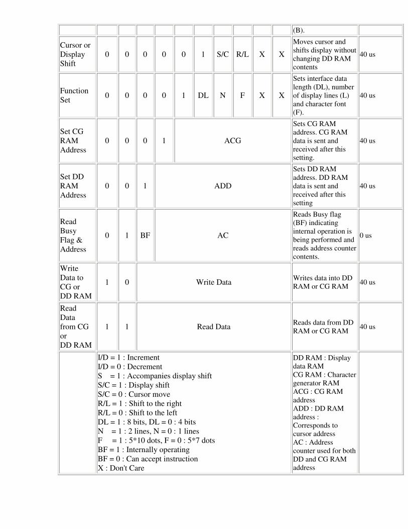
(B).
Cursor or Display Shift
0 0 0 0 0 1 S/C R/L X X
Moves cursor and shifts display without changing DD RAM contents
40 us
Function Set 0 0 0 0 1 DL N F X X
Sets interface data length (DL), number of display lines (L) and character font (F).
40 us
Set CG RAM Address
0 0 0 1 ACG
Sets CG RAM address. CG RAM data is sent and received after this setting.
40 us
Set DD RAM Address
0 0 1 ADD
Sets DD RAM address. DD RAM data is sent and received after this setting
40 us
Read Busy Flag & Address
0 1 BF AC
Reads Busy flag (BF) indicating internal operation is being performed and reads address counter contents.
0 us
Write Data to CG or DD RAM
1 0 Write Data Writes data into DD RAM or CG RAM 40 us
Read Data from CG or DD RAM
1 1 Read Data Reads data from DD RAM or CG RAM 40 us
I/D = 1 : Increment I/D = 0 : Decrement S = 1 : Accompanies display shift S/C = 1 : Display shift S/C = 0 : Cursor move R/L = 1 : Shift to the right R/L = 0 : Shift to the left DL = 1 : 8 bits, DL = 0 : 4 bits N = 1 : 2 lines, N = 0 : 1 lines F = 1 : 5*10 dots, F = 0 : 5*7 dots BF = 1 : Internally operating BF = 0 : Can accept instruction X : Don't Care
DD RAM : Display data RAM CG RAM : Character generator RAM ACG : CG RAM address ADD : DD RAM address : Corresponds to cursor address AC : Address counter used for both DD and CG RAM address

Notes:
• After power on, the LCD has to wait more than 15 ms for Vcc rises to 4.5V before accepting the first instruction.
• I set signal "count" count from 0 to 3. However, this value is depend on the system clock. Make sure the LCD has enough time to execute the next instruction. Execution time for each instruction(Follow the instruction table).
• VHDL example for LCD display Initialization
--------------------------------------------------------------------------------------------------- -- File : lcd_init.vhd -- Entity : lcd_init --------------------------------------------------------------------------------------------------- -- University : Vishweswaraia Technological University Belgaum,Karnataka -- Simulators : Mentor Graphics Modelsim -- Synthesizers : Xilinx ISE -- Target Device : XC4000 Series ------------------------------------------------------------------------------------------------ -- Description : This program initialize the LCD display ----------------------------------------------------------------------------------------------- --The IEEE standard 1164 package, declares std_logic, etc. library IEEE; use IEEE.Std_Logic_1164.all; use IEEE.Std_Logic_unsigned.all; use IEEE.NUMERIC_STD.all; ---------------------------------- Entity Declarations ------------------------- entity lcd_init is generic(width : positive := 8); port(reset, clock, enable, done_ack : in std_logic; done, RW, rs, lcd_e : out std_logic; Qout : buffer std_logic_vector(width-1 downto 0) ); end lcd_init; architecture initial of lcd_init is type state_type is (waiting, i0, i1, i2, i3, donestate); signal state, next_state : state_type; signal count,count_temp : std_logic_vector(1 downto 0); signal Qout_temp : std_logic_vector(width-1 downto 0); begin running : process(state,enable,done_ack,count) is

begin case state is when waiting => done <= '0'; lcd_e <= '1'; RW <= '0'; rs <= '0'; Qout_temp <= "00000000"; if enable = '1' then next_state <= i0; else next_state <= waiting; end if; when i0 => Qout_temp <= "00000001"; --clear display if count = "11" then next_state <= i1; else next_state <= i0; end if; when i1 => Qout_temp <= "00000010"; --clear display & returns to HOME if count = "11" then next_state <= i2; else next_state <= i1; end if; when i2 => Qout_temp <= "00111000"; --2 line display if count = "11" then next_state <= i3; else next_state <= i2; end if; when i3 => Qout_temp <= "00001110"; --truns on display with cursor at home if count = "11" then next_state <= donestate; else next_state <= i3;

end if; when donestate => done <= '1'; Qout_temp <= ( others => '0' ); if done_ack = '1' then next_state <= waiting; else next_state <= donestate; end if; end case; end process running; timing : process(clock,reset) is begin if rising_edge(clock) then Qout <= Qout_temp; count <= count_temp; if reset = '1' then state <= waiting; count_temp <= "00"; else state <= next_state; count_temp <= count_temp + "01"; end if; end if; end process timing; end initial;

• Simulator waveforms for LCD display Initialization:
clock
reset
enable
done_ack
done
RW
rs
lcd_e
Qout
state
next_state
count
count_temp
Qout_temp
ns200 400 600 800 1000 1200 1400 1600
00 01 02 38 0E
waiting i0 i1 i2 i3
waiting i1 i2 i3
U 0 1 2 3 0 1 2 3 0 1 2 3 0 1 2 3 0 1
0 1 2 3 0 1 2 3 0 1 2 3 0 1 2 3 0 1 2
00 01 02 38 0E
00
donestate
donestate
00
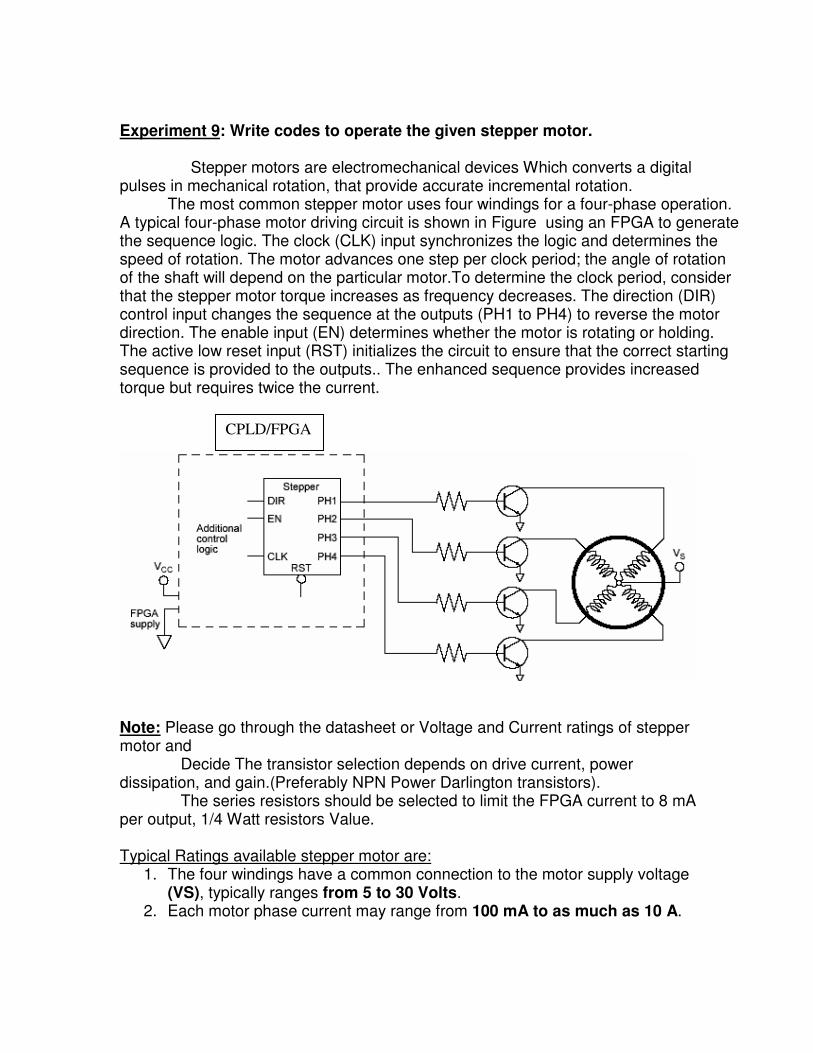
Experiment 9: Write codes to operate the given stepper motor. Stepper motors are electromechanical devices Which converts a digital pulses in mechanical rotation, that provide accurate incremental rotation.
The most common stepper motor uses four windings for a four-phase operation. A typical four-phase motor driving circuit is shown in Figure using an FPGA to generate the sequence logic. The clock (CLK) input synchronizes the logic and determines the speed of rotation. The motor advances one step per clock period; the angle of rotation of the shaft will depend on the particular motor.To determine the clock period, consider that the stepper motor torque increases as frequency decreases. The direction (DIR) control input changes the sequence at the outputs (PH1 to PH4) to reverse the motor direction. The enable input (EN) determines whether the motor is rotating or holding. The active low reset input (RST) initializes the circuit to ensure that the correct starting sequence is provided to the outputs.. The enhanced sequence provides increased torque but requires twice the current.
Note: Please go through the datasheet or Voltage and Current ratings of stepper motor and Decide The transistor selection depends on drive current, power dissipation, and gain.(Preferably NPN Power Darlington transistors). The series resistors should be selected to limit the FPGA current to 8 mA per output, 1/4 Watt resistors Value. Typical Ratings available stepper motor are:
1. The four windings have a common connection to the motor supply voltage (VS), typically ranges from 5 to 30 Volts.
2. Each motor phase current may range from 100 mA to as much as 10 A.
CPLD/FPGA

Stepper motor sequencing: There are several kinds of sequences that can be used to drive stepper motors. The following tables give the most common sequences for energizing the coils. Following the steps in ascending order drives the motor in one direction, going in descending order drives the motor the other way. This sequence interleaves the normal and wave sequences.
If step angle = 1.8, For One revolution 360/1.8=200 steps(In Full step mode)
If step angle = 0.9, For One revolution 360/0.9=400 steps(In Half step mode) Bipolar stepper motor will not run in Half step mode for any consult the stepper motor manufacturer.
Full step
Steps Q1 Q2 Q3 Q4 Step0 1 0 1 0 Step1 1 0 0 1 Step2 1 0 1 0 Step3 0 1 1 0
Make this sequence in Descending order motor rotates in opposite direction(This sequence will be provided by the stepper motor manufacturer).
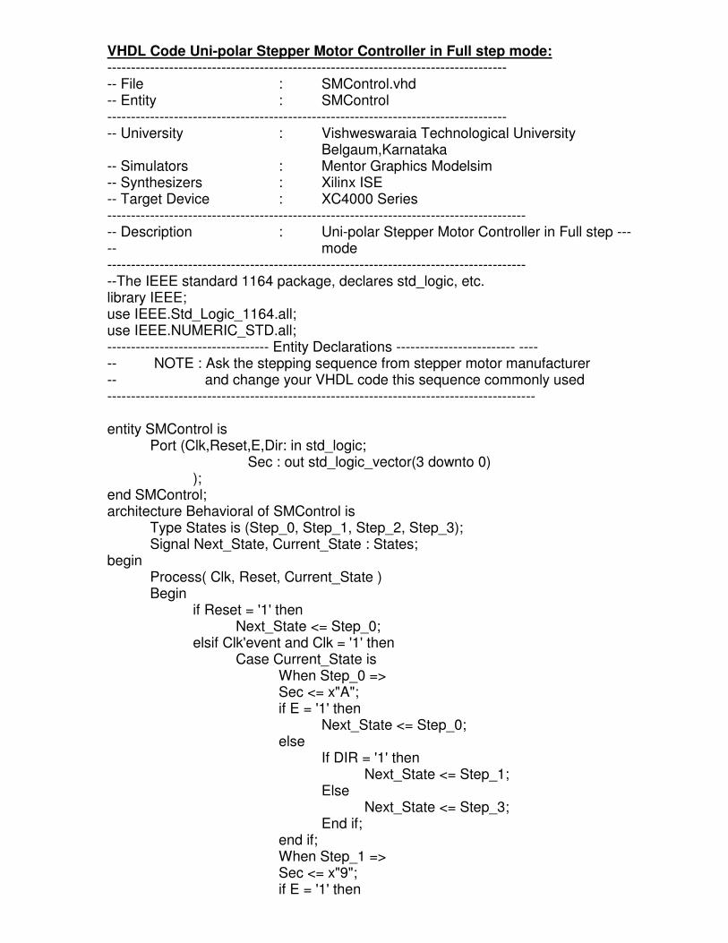
VHDL Code Uni-polar Stepper Motor Controller in Full step mode: ------------------------------------------------------------------------------------ -- File : SMControl.vhd -- Entity : SMControl ------------------------------------------------------------------------------------ -- University : Vishweswaraia Technological University Belgaum,Karnataka -- Simulators : Mentor Graphics Modelsim -- Synthesizers : Xilinx ISE -- Target Device : XC4000 Series ---------------------------------------------------------------------------------------- -- Description : Uni-polar Stepper Motor Controller in Full step ----- mode ---------------------------------------------------------------------------------------- --The IEEE standard 1164 package, declares std_logic, etc. library IEEE; use IEEE.Std_Logic_1164.all; use IEEE.NUMERIC_STD.all; ---------------------------------- Entity Declarations ------------------------- ---- -- NOTE : Ask the stepping sequence from stepper motor manufacturer -- and change your VHDL code this sequence commonly used ------------------------------------------------------------------------------------------ entity SMControl is Port (Clk,Reset,E,Dir: in std_logic; Sec : out std_logic_vector(3 downto 0) ); end SMControl; architecture Behavioral of SMControl is Type States is (Step_0, Step_1, Step_2, Step_3); Signal Next_State, Current_State : States; begin Process( Clk, Reset, Current_State ) Begin if Reset = '1' then Next_State <= Step_0; elsif Clk'event and Clk = '1' then Case Current_State is When Step_0 => Sec <= x"A"; if E = '1' then Next_State <= Step_0; else If DIR = '1' then Next_State <= Step_1; Else Next_State <= Step_3; End if; end if; When Step_1 => Sec <= x"9"; if E = '1' then
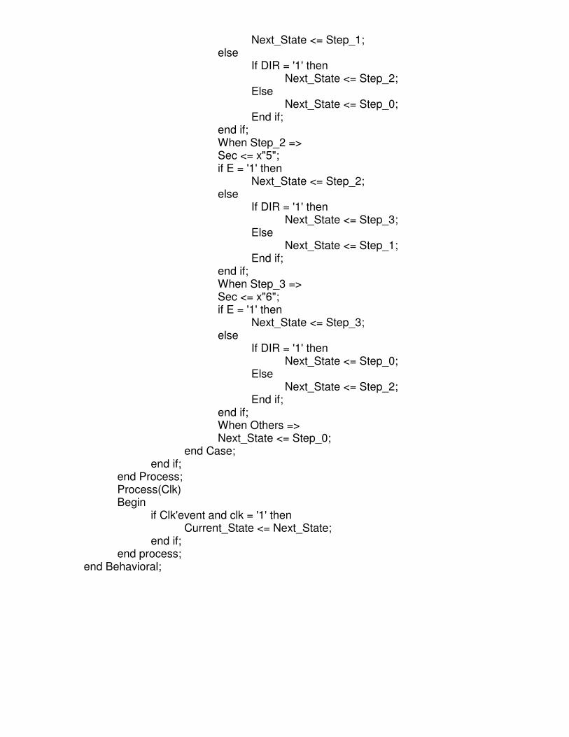
Next_State <= Step_1; else If DIR = '1' then Next_State <= Step_2; Else Next_State <= Step_0; End if; end if; When Step_2 => Sec <= x"5"; if E = '1' then Next_State <= Step_2; else If DIR = '1' then Next_State <= Step_3; Else Next_State <= Step_1; End if; end if; When Step_3 => Sec <= x"6"; if E = '1' then Next_State <= Step_3; else If DIR = '1' then Next_State <= Step_0; Else Next_State <= Step_2; End if; end if; When Others => Next_State <= Step_0; end Case; end if; end Process; Process(Clk) Begin if Clk'event and clk = '1' then Current_State <= Next_State; end if; end process; end Behavioral;

State machine Diagram according to step changes:
Simulator waveforms for Uni-polar Stepper Motor Controller in Full step mode:
Clk
Reset
E
Dir
Sec
Sec(3)
Sec(2)
Sec(1)
Sec(0)
Next_State
Current_State
ns1400 1600 1800 2000 2200 2400 2600 2800 3000
5 9 A 6 5 9 A 9 5 6
step_1 step_0 step_3 step_2 step_1 step_0 step_1 step_2 step_3 step_0
step_2 step_1 step_0 step_3 step_2 step_1 step_0 step_1 step_2 step_3 step_0