Diffraction phase microscopy: principles and applications...
63
Diffraction phase microscopy: principles and applications in materials and life sciences Basanta Bhaduri, 1 Chris Edwards, 2 Hoa Pham, 1 Renjie Zhou, 2 Tan H. Nguyen, 1 Lynford L. Goddard, 2 and Gabriel Popescu 1,* 1 Quantitative Light Imaging Laboratory, Department of Electrical and Computer Engineering, Beckman Institute for Advanced Science and Technology, University of Illinois at Urbana-Champaign, Urbana, Illinois 61801, USA 2 Micro and Nanotechnology Laboratory, Department of Electrical and Computer Engineering, University of Illinois at Urbana-Champaign, Urbana, Illinois 61801, USA *Corresponding author: [email protected] Received July 9, 2013; revised January 5, 2014; accepted January 27, 2014; published March 26, 2014 (Doc. ID 193585) The main obstacle in retrieving quantitative phase with high sensitivity is posed by the phase noise due to mechanical vibrations and air fluctuations that typically affect any interferometric system. In this paper, we review diffraction phase microscopy (DPM), which is a common-path quantitative phase imaging (QPI) method that significantly alleviates the noise problem. DPM utilizes a compact Mach–Zehnder interferometer to combine several attributes of current QPI methods. This compact configuration inherently cancels out most mechanisms responsible for noise and is single-shot, mean- ing that the acquisition speed is limited only by the speed of the camera employed. This technique is also nondestructive and does not require stain- ing or coating of the specimen. This unique collection of features enables the DPM system to accurately monitor the dynamics of various nanoscale phenomena in a wide variety of environments. The DPM system can oper- ate in both transmission and reflection modes in order to accommodate both transparent and opaque samples, respectively. Thus, current applications of DPM include measuring the dynamics of biological samples, semiconductor wet etching and photochemical etching processes, surface wetting and evaporation of water droplets, self-assembly of nanotubes, expansion and deformation of materials, and semiconductor wafer defect detection. Finally, DPM with white light averages out much of the speckle background and also offers potential for spectroscopic measurements. © 2014 Optical Society of America OCIS codes: (050.1950) Diffraction gratings; (110.0180) Micros- copy; (120.3890) Medical optics instrumentation; (120.3940) Metrology; (120.5050) Phase measurement; (110.3175) Interferomet- ric imaging http://dx.doi.org/10.1364/AOP.6.000057 Advances in Optics and Photonics 6, 57–119 (2014) doi:10.1364/AOP .6.000057 57 1943-8206/14/010057-63$15/0$15.00 © OSA
Transcript of Diffraction phase microscopy: principles and applications...

Diffraction phase microscopy: principlesand applications in materials and lifesciencesBasanta Bhaduri,1 Chris Edwards,2 Hoa Pham,1 Renjie Zhou,2
Tan H. Nguyen,1 Lynford L. Goddard,2 and Gabriel Popescu1,*
1Quantitative Light Imaging Laboratory, Department of Electrical and ComputerEngineering, Beckman Institute for Advanced Science and Technology, University ofIllinois at Urbana-Champaign, Urbana, Illinois 61801, USA
2Micro and Nanotechnology Laboratory, Department of Electrical and ComputerEngineering, University of Illinois at Urbana-Champaign, Urbana, Illinois 61801, USA
*Corresponding author: [email protected]
Received July 9, 2013; revised January 5, 2014; accepted January 27, 2014; publishedMarch 26, 2014 (Doc. ID 193585)
The main obstacle in retrieving quantitative phase with high sensitivity isposed by the phase noise due to mechanical vibrations and air fluctuationsthat typically affect any interferometric system. In this paper, we reviewdiffraction phase microscopy (DPM), which is a common-path quantitativephase imaging (QPI) method that significantly alleviates the noise problem.DPM utilizes a compact Mach–Zehnder interferometer to combine severalattributes of current QPI methods. This compact configuration inherentlycancels out most mechanisms responsible for noise and is single-shot, mean-ing that the acquisition speed is limited only by the speed of the cameraemployed. This technique is also nondestructive and does not require stain-ing or coating of the specimen. This unique collection of features enablesthe DPM system to accurately monitor the dynamics of various nanoscalephenomena in a wide variety of environments. The DPM system can oper-ate in both transmission and reflection modes in order to accommodate bothtransparent and opaque samples, respectively. Thus, current applications ofDPM include measuring the dynamics of biological samples, semiconductorwet etching and photochemical etching processes, surface wetting andevaporation of water droplets, self-assembly of nanotubes, expansion anddeformation of materials, and semiconductor wafer defect detection. Finally,DPM with white light averages out much of the speckle backgroundand also offers potential for spectroscopic measurements. © 2014 OpticalSociety of America
OCIS codes: (050.1950) Diffraction gratings; (110.0180) Micros-copy; (120.3890) Medical optics instrumentation; (120.3940)Metrology; (120.5050) Phase measurement; (110.3175) Interferomet-ric imaginghttp://dx.doi.org/10.1364/AOP.6.000057
Advances in Optics and Photonics 6, 57–119 (2014) doi:10.1364/AOP.6.000057 571943-8206/14/010057-63$15/0$15.00 © OSA

1. Introduction. . . . . . . . . . . . . . . . . . . . . . . . . . . . . . . . . . . . . . . . 592. Principles of DPM . . . . . . . . . . . . . . . . . . . . . . . . . . . . . . . . . . . 60
2.1. Theory. . . . . . . . . . . . . . . . . . . . . . . . . . . . . . . . . . . . . . . . 602.2. Design Principles. . . . . . . . . . . . . . . . . . . . . . . . . . . . . . . . . 63
2.2a. Transverse Resolution . . . . . . . . . . . . . . . . . . . . . . . . . . 632.2b. Sampling: Grating Period and Pixel Size . . . . . . . . . . . . . 642.2c. Field of View (Lens Selection in 4f Configuration). . . . . . 662.2d. Fourier Plane Spacing (Filter Construction) . . . . . . . . . . . 662.2e. Pinhole Size (Uniform Reference at CCD Plane). . . . . . . . 67
2.3. Phase Reconstruction . . . . . . . . . . . . . . . . . . . . . . . . . . . . . . 692.4. System Testing and Noise Characterization . . . . . . . . . . . . . . . 722.5. Derivative Method for Phase Reconstruction . . . . . . . . . . . . . . 74
3. Laser DPM . . . . . . . . . . . . . . . . . . . . . . . . . . . . . . . . . . . . . . . . 763.1. Transmission Mode . . . . . . . . . . . . . . . . . . . . . . . . . . . . . . . 76
3.1a. Setup . . . . . . . . . . . . . . . . . . . . . . . . . . . . . . . . . . . . . 763.1b. Applications . . . . . . . . . . . . . . . . . . . . . . . . . . . . . . . . 77
3.2. Reflection Mode . . . . . . . . . . . . . . . . . . . . . . . . . . . . . . . . . 823.2a. Setup . . . . . . . . . . . . . . . . . . . . . . . . . . . . . . . . . . . . . 823.2b. Applications . . . . . . . . . . . . . . . . . . . . . . . . . . . . . . . . 82
4. White-Light DPM . . . . . . . . . . . . . . . . . . . . . . . . . . . . . . . . . . . 914.1. Setup. . . . . . . . . . . . . . . . . . . . . . . . . . . . . . . . . . . . . . . . . 914.2. Role of Coherence in wDPM . . . . . . . . . . . . . . . . . . . . . . . . 93
4.2a. Temporal Coherence. . . . . . . . . . . . . . . . . . . . . . . . . . . 934.2b. Spatial Coherence . . . . . . . . . . . . . . . . . . . . . . . . . . . . 94
4.3. Applications . . . . . . . . . . . . . . . . . . . . . . . . . . . . . . . . . . . . 954.3a. Red Blood Cell Membrane Fluctuation Measurement. . . . . 954.3b. QPI of Beating Cardiomyocyte Cell . . . . . . . . . . . . . . . . 954.3c. Cell Growth Study . . . . . . . . . . . . . . . . . . . . . . . . . . . . 96
4.4. Spectroscopic DPM . . . . . . . . . . . . . . . . . . . . . . . . . . . . . . . 974.4a. Existing Approaches . . . . . . . . . . . . . . . . . . . . . . . . . . . 974.4b. Spectroscopic DPM with White Light . . . . . . . . . . . . . . . 98
5. Real-Time DPM . . . . . . . . . . . . . . . . . . . . . . . . . . . . . . . . . . . 1005.1. Real-Time Phase Reconstruction Using Graphics
Processing Units . . . . . . . . . . . . . . . . . . . . . . . . . . . . . . . . . 1015.1a. Phase Extraction Module. . . . . . . . . . . . . . . . . . . . . . . 1015.1b. CUDA-Based Phase Unwrapping Algorithm. . . . . . . . . . 1025.1c. Performance Results . . . . . . . . . . . . . . . . . . . . . . . . . . 104
5.2. Applications . . . . . . . . . . . . . . . . . . . . . . . . . . . . . . . . . . . . 1045.2a. Single Cell Parameters Computed in Real Time . . . . . . . 1065.2b. Cell Segmentation and Connected Component Labeling . . 1065.2c. Results . . . . . . . . . . . . . . . . . . . . . . . . . . . . . . . . . . . 107
6. Summary and Discussion . . . . . . . . . . . . . . . . . . . . . . . . . . . . . 108References . . . . . . . . . . . . . . . . . . . . . . . . . . . . . . . . . . . . . . . . . 109
Advances in Optics and Photonics 6, 57–119 (2014) doi:10.1364/AOP.6.000057 58
Diffraction phase microscopy: principlesand applications in materials and lifesciencesBasanta Bhaduri, Chris Edwards, Hoa Pham, Renjie Zhou,Tan H. Nguyen, Lynford L. Goddard, and Gabriel Popescu
1. Introduction
Ever since the development of phase contrast microscopy in the 1930s by FritzZernike, it has been realized that the phase of light is an extremely powerfulreporter on specimen morphology and topography [1,2]. This principle stemsfrom the knowledge that an ideal imaging system produces an image field thatis a scaled replica of the sample field in both amplitude and phase. Thus, phasesensitive measurements at the image plane relate to the local optical properties(refractive index, thickness) of the object under investigation. Phase contrastmicroscopy made such an important impact in biology that it earned Zernikethe Nobel Prize in Physics in 1953.
In 1948, Gabor published his famous paper entitled “A new microscopic prin-ciple,” in which he proposed the use of optical phase information to correct aber-rations in electron micrographs [3]. While the proposed method has never trulysolved the aberration issues in electron microscopy, it generated instead a newoptical field—holography—for which Gabor received the Nobel Prize inPhysics in 1971. In essence, Gabor, an electrical engineer with knowledge ofcommunication theory [4], introduced the idea that imaging is a form of trans-mission of information. Interestingly, the spatial analog to a carrier frequencywas introduced much later by Lohmann [5] and by Leith and Upatnieks [6]. Thisapproach, known as off-axis holography, has a major practical advantage overGabor’s original idea (in-line holography) as it can decouple the contributionsbetween the illuminating wave and the field scattered by the object. The firstdemonstration of the feasibility of the numerical reconstruction of hologramswas performed by Goodman and Lawrence [7]. A fast Fourier transform methodfor analyzing fringes in off-axis holography was reported by Takeda et al. in1982 and became broadly adopted in the field [8]. The impact of digital holog-raphy on microscopy became significant much later in the 1990s when imple-mented with charge-coupled devices (CCDs) as the detector. In 1994 Schnarsand Jüptner demonstrated “lensless” off-axis digital holography using a CCD asdetector [9]. Soon after, the benefits of digital holography were exploited inmicroscopy by several groups, in particular, the groups led by Yamaguchi[10], Depeursinge [11], von Bally [12,13], Ferraro [14,15], Kim [16–18],Wax [19–21], Asundi [22,23], Poon [24], and others [25–28].
Interferometry and holography have become invaluable tools in optical metrol-ogy, especially because they provide information about material topographywith nanoscale accuracy [29]. Since the 1950s, scientists have recognizedthe potential of optical phase to provide quantitative information about
Advances in Optics and Photonics 6, 57–119 (2014) doi:10.1364/AOP.6.000057 59

biological specimens, including cell dry mass [30,31]. In the past two decades,quantitative phase imaging (QPI), in which the optical path-length map across aspecimen is measured, has become a rapidly emerging field with important ap-plications in biomedicine [32]. QPI utilizes the fact that the phase of a field ismuch more sensitive to the specimen structure than its amplitude. As fields fromthe source interact with the specimen, phase shifts are induced in the scatteredfield with respect to the unscattered light. This phase shift contains the desiredstructural information about the sample under investigation. Because of thenature of photon absorption, and the limited speed of electronic components,cameras and detectors can measure only intensity. To obtain the phase informa-tion, interferometric as well as non-interferometric methods are employed.Recently, a number of such methods have been developed by variousgroups around the world for quantitatively imaging biological specimens[16–20,33–46].
The main obstacle in retrieving quantitative phase images with high sensitivity isposed by the phase noise due to mechanical vibrations and air fluctuations thattypically affect any interferometric system. In this paper, we review diffractionphase microscopy (DPM) [42], which is a common-path QPI method that sig-nificantly alleviates the noise problem. DPM utilizes a compact Mach–Zehnderinterferometer to combine all of the best attributes of current QPI methods in anefficient and elegant manner. This compact configuration is common-path,which inherently cancels out most mechanisms responsible for noise, and issingle-shot, meaning that the acquisition speed is limited only by the speedof the camera employed. This technique is also nondestructive and does notrequire staining or coating of the specimen. This unique collection of featuresenables the DPM system to accurately monitor the dynamics of various nano-scale phenomena in a wide variety of environments. The DPM system can op-erate in both transmission and reflection modes in order to accommodate bothtransparent and opaque samples. Thus, current applications of DPM includemeasuring the dynamics of biological samples, semiconductor wet etchingand photochemical etching processes, surface wetting and evaporation of waterdroplets, self-assembly of nanotubes, expansion and deformation of materials,and semiconductor wafer defect detection. Finally, DPM with white light aver-ages out much of the speckle background and also offers potential for spectro-scopic measurements.
This review aims at summarizing the principles of the DPM operation, thedesign constraints, its various experimental implementations and applicationsin materials and life sciences.
2. Principles of DPM
2.1. Theory
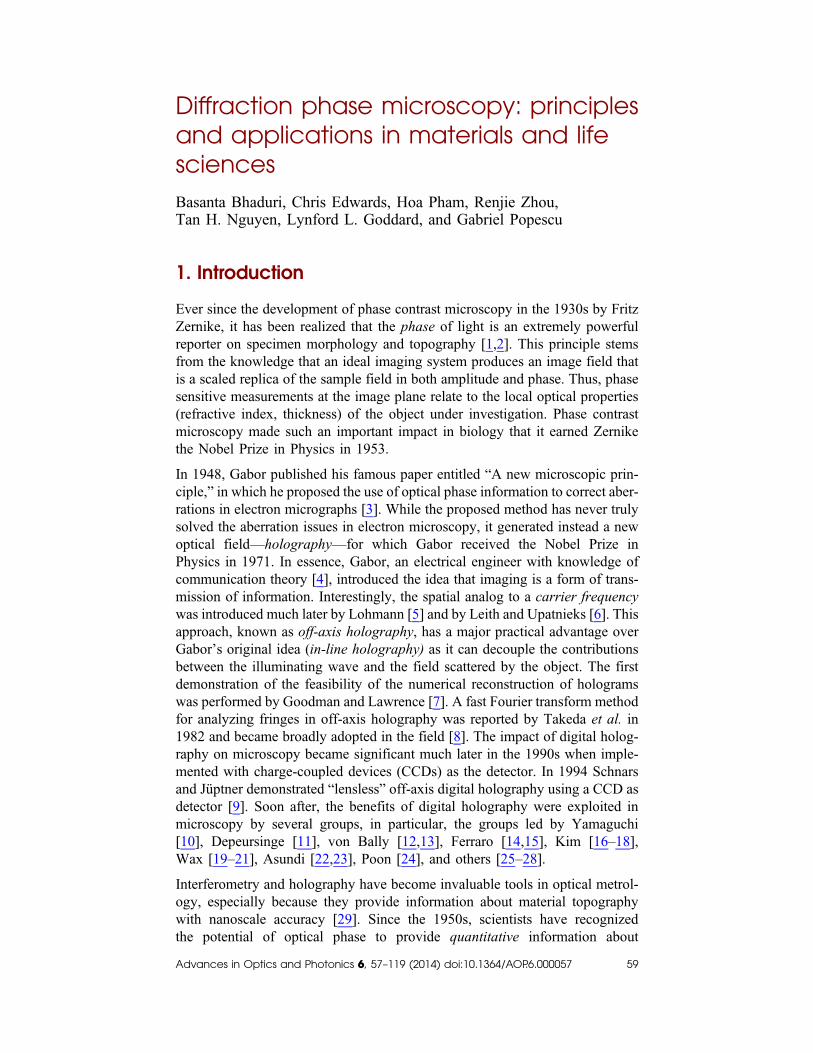
Figure 1 shows a schematic of the DPM system, which can be placed at theoutput port of any conventional light microscope. The DPM interferometer iscreated using a diffraction grating in conjunction with a 4f lens system. In thisgeometry, the interferometer is very stable, allowing highly sensitive time-resolved measurements.
Because of the periodic nature of the diffraction grating, multiple copies of theimage are created at different angles. Here, we are concerned only with the
Advances in Optics and Photonics 6, 57–119 (2014) doi:10.1364/AOP.6.000057 60
0th and +1st orders, which create the final interferogram at the CCD plane. Theother orders either do not pass through the first lens or are filtered out in theFourier plane.
Starting in the grating plane (denoted by the subscript GP) we have
UGP�x; y� � U0�x; y� � U1�x; y�eiβx; (2.1-1)
where U 0 is the 0th order field and U 1 is the +1st order field. Here, β ≡ 2π∕Λ,where Λ is the grating period. The two fields have the same spatial distributionbut may have different amplitudes depending on the grating efficiency. For ex-ample, a blazed grating can be used to make the +1st order have much higheramplitude so that, after filtering, the amplitudes are better matched and the fringevisibility on the final interferogram is more optimal.
The first 2f system takes a Fourier transform of this field such that before thefilter in the Fourier plane (denoted by the subscript FP–) we have
~UFP−�kx; ky� � ~U 0�kx; ky� � ~U 1�kx − β; ky�; (2.1-2a)
Figure 1
DPM. (a) A diffraction grating is used in conjunction with a 4f system in orderto produce interference and obtain the phase information from the scatteredfields. The grating is placed at the output image plane of the microscope, whichcreates copies of the image at different angles, some of which are captured by thefirst lens. Under a 4f configuration, the first lens takes a Fourier transform, cre-ating a Fourier plane. (b) A spatial filter is placed in the Fourier plane, whichallows the full 0th order to pass, and the 1st order is filtered down using a smallpinhole such that after the second lens takes a Fourier transform, the field be-comes a uniform plane wave and serves as the reference to the interferometer.The two fields interfere at the final image plane on the CCD sensor to create theinterferogram.
Advances in Optics and Photonics 6, 57–119 (2014) doi:10.1364/AOP.6.000057 61

kx � 2πx1∕�λf 1� ≡ αx1; ky � 2πy1∕�λf 1� ≡ αy1; (2.1-2b)
β � 2π∕Λ � 2πΔx∕�λf 1� ≡ αΔx; Δx � λf 1∕Λ; (2.1-2c)
where �x1; y1� are the coordinates at the Fourier plane. Equation (2.1-2b) showsthe relationship between the angular spatial frequency variables and their actuallocation in free space. The quantity Δx represents the physical spacing betweenthe two diffraction orders in the Fourier plane. This value will be re-derived inthe next section using simple geometrical optics and used in the design process.From Eq. (2.1-2a), we can see that we have two separate Fourier transforms ofthe image separated in space.
Because we chose a blazed grating, the 1st order is brighter than the 0th order inthe Fourier plane. It is filtered down using a small enough pinhole such that afterpassing through the second lens this field approaches a plane wave at the cameraplane where the transverse amplitude and phase are uniform. This beam servesas our reference for the interferometer. Immediately after the pinhole (denotedby the subscript FP�), we have
~UFP��αx1; αy1� � ~U 0�αx1; αy1� � ~U 1�αx1 − β; αy1� � δ�αx1 − β; αy1�� ~U 0�αx1; αy1� � ~U 1�0; 0�δ�αx1 − β; αy1�. (2.1-3)
In Eq. (2.1-3), ~U1�0; 0�δ�αx1 − β; αy1� is the spatial frequency domain represen-tation of the DC signal and ~U 0�αx1; αy1� is the unfiltered signal that contains theimage information. So, in the Fourier plane we have one beam carrying all of theinformation contained in the original image (0th order) and a second beam whichcarries only the DC content of the original image and serves as our referencebeam (1st order).
The second 2f system takes another forward Fourier transform, resulting in
F:Tf ~UFP��αx1; αy1�g � F:Tf ~U 0�αx1; αy1� � ~U1�0; 0�δ�αx1 − β; αy1�g
� 1
jαj �U0�ξ∕α; η∕α� � ~U 1�0; 0�e−iξβ∕α�; (2.1-4a)
ξ ≡ 2πx∕λf 2; η ≡ 2πy∕λf 2: (2.1-4b)
At the camera plane (denoted by the subscript CP), the resulting field is
UCP�x; y� �1
jαj �U 0�−x∕M 4f ;−y∕M4f � � U1�0; 0�eiβx∕M4f �; (2.1-5a)
M4f ≡ −f 2∕f 1; (2.1-5b)
where terms containing α, ξ, and η have been canceled out and the magnificationof the 4f system, M 4f , has been substituted into the equation.
In deriving the irradiance on the CCD camera, we write U 0 and U 1 in phasorform as
U 0�x; y� ≡ A0�x; y�eiϕ0�x;y�; U1�x; y� ≡ A1�x; y�eiϕ1�x;y�: (2.1-6)
Advances in Optics and Photonics 6, 57–119 (2014) doi:10.1364/AOP.6.000057 62

Now, Eq. (2.1-5a) becomes
UCP�x; y� �1
jαj �A0�−x∕M 4f ;−y∕M4f �eiϕ0�−x∕M4f ;−y∕M4f �
� A1�0; 0�eiβx∕M4f eiϕ1�0;0��: (2.1-7)
To further simplify, on the right-hand side we change −x∕M 4f → x0,−y∕M 4f → y0, A0∕jαj → A0
0, A1∕jαj → A01, so
UCP�x; y� � A00�x0; y0�eiϕ0�x0;y0� � A0
1e−iβx0eiϕ1 : (2.1-8)
At the camera plane we have the interference of two magnified copies of theimage, where one is filtered to DC, and both are inverted in x and y. The in-version results because two forward transforms are taken by the lenses ratherthan a transform pair. The resulting intensity measured at the CCD is as follows:
ICP�x0; y0� � UCP�x; y�U�CP�x; y�
� jA00�x0; y0�j2 � jA0
1j2 � 2jA01jjA0
0�x0; y0�j cos�βx0 � Δϕ�; (2.1-9a)
ICP�x0; y0� � I0�x0; y0� � I1 � 2ffiffiffiffiffiffiffiffiffiffiffiffiffiffiffiffiffiffiffiffiI0�x0; y0�I1
pcos�βx0 � Δϕ�; (2.1-9b)
Δϕ � ϕ0�x0; y0� − ϕ1. (2.1-9c)
The phase information from the sample can be extracted from the modulation(cosine) term which is a result of the interference between the image and thereference beam.
2.2. Design Principles
When designing a DPM system, the final transverse resolution of the image isdetermined by two parameters: the optical resolution of the microscope and theperiod of the grating, as detailed below.
2.2a. Transverse Resolution
For a microscope operating in transmission mode, with NAobj and NAcon theobjective and condenser numerical apertures, the resolution is given by Abbe’sformula [47]:
Δρ � 1.22λ
�NAobj � NAcon�
≃1.22λ
NAobj
; (2.2-1)
where we assumed plane wave illumination (NAcon ≃ 0). The resolution ob-tained from Abbe’s formula is calculated according to the Rayleigh criterion,and the quantity Δρ represents the diffraction spot radius or the distance fromthe peak to the first zero of the Airy pattern. The resolution of our DPM systemranges from approximately 700 nm (63×, 0.95 NA) to 5 μm (5×, 0.13 NA) de-pending on the objective being used. To get better resolution at a given wave-length, a higher NA is required. This is typically obtained by using a higher
Advances in Optics and Photonics 6, 57–119 (2014) doi:10.1364/AOP.6.000057 63

magnification objective that captures larger angles from the sample plane. Ahigher NA typically means a higher magnification, which results in a smallerfield of view (FOV).
2.2b. Sampling: Grating Period and Pixel Size
The grating is essentially sampling the image. Thus, unless the grating period issufficiently fine, this sampling degrades the native optical resolution of the mi-croscope. Intuitively, as a result of the Nyquist theorem, we may expect that twoperiods per diffraction spot give the minimum grating period. It turns out that,due to the interferometric setup, this number must be slightly revised. To under-stand the frequency coverage of the interferogram, we take the Fourier transformof Eq. (2.1-9a) and obtain
~ICP�kx; ky� � FT�ICP�x0; y0��� FT�U 0�x0; y0�U�
0�x0; y0� � U 1U�1 � U 0�x0; y0�U�
1eiβx0
� U�0�x0; y0�U1e
−iβx0 �� ~U 0�kx; ky�Ⓥ ~U�
0�−kx;−ky� � jU 1j2δ�kx; ky�� ~U0�kx; ky�U�
1 Ⓥ δ�kx − β; ky� � ~U�0�−kx;−ky�U 1 Ⓥ δ�kx � β; ky�:
(2.2-2)
In Eq. (2.2-2), we used the correlation theorem for Fourier transformations,i.e., U0�x; y�U�
0�x; y� → ~U 0�kx; ky�Ⓥ ~U�0�−kx;−ky�; the shift theorem, i.e.,
eiβx0→ δ�kx − β; ky�, the convolution theorem, i.e., U 0�x; y�U�
1eiβx0 →
~U 0�kx; ky�U 1 Ⓥ δ�kx − β; ky�; and the assumption thatU 1 is uniform after passingthrough the pinhole filter, i.e., U1U 1� → jU1j2δ�kx; ky�; (symbol Ⓥ denotes theconvolution operation). Note that the convolution of a function with the flippedversion of itself, ~U 0�kx; ky�Ⓥ ~U�
0�−kx;−ky�, amounts to an autocorrelation.
Figure 2 shows the Fourier transform of the DPM interferogram represented inthe sample plane. Because of interference [Eq. (2.1-9a)], the radius of the centrallobe is 2k0NAobj and the radius of the sidelobes is k0NAobj. To avoid aliasingerrors from overlapping frequencies in the Fourier plane, the grating modulationfrequency must be chosen such that
β ≥ 3k0NAobj; (2.2-3a)
where modulation frequency β (in the sample plane) is defined asβ � �2π∕Λ�Mobj, with Λ the period of the grating and M obj the magnificationof the microscope. Thus, from the sampling constraint above, we find that
Λ ≤λM obj
3NAobj
: (2.2-3b)
This is the basic criterion and provides an upper bound on the selection of thegrating period. Expressing NAobj in terms of the diffraction spot size usingEq. (2.2-1), we find
Λ ≤ΔρMobj
3.66: (2.2-3c)
This states that we need at least 3.66 grating fringes per diffraction spot radius inorder to operate at optimal resolution and avoid aliasing.
Advances in Optics and Photonics 6, 57–119 (2014) doi:10.1364/AOP.6.000057 64

To properly sample the interferogram by the CCD pixels, the Nyquist theoremdemands that
ks ≥ 2kmax � 2�β� k0NAobj�; (2.2-4)
where ks is the pixel sampling frequency, andM 4f is the magnification of the 4fsystem that images the grating at the CCD plane. This magnification can be usedas a tuning knob for the system as it can adjust the grating period relative to thepixel size at the CCD plane. If we denote the physical pixel size of the camera asa, the constraint necessary to avoid aliasing due to pixel sampling is
ks �2π
aMobjjM 4f j ≥ 2�β� k0NAobj�; (2.2-5a)
which leads to
jM 4f j ≥ 2a
�1
Λ� 1
λ
NAobj
Mobj
�: (2.2-5b)
This is another important criterion stating the minimum 4f magnification for agiven grating period. Note that if Eq. (2.2-3b) holds and if
Figure 2
Fourier transform of the intensity at the CCD as represented in the sample plane.Because of interference, the radius of the central lobe is 2k0NAobj and the radiusof the sidelobes is k0NAobj. To avoid aliasing effects and allow for properreconstruction of the desired signal, the modulation frequency β must be≥3k0NAobj and the sampling (pixel) frequency ks ≥ 2�β� k0NAobj�. (a) Alias-ing as a result of the grating period being too large. (b) Grating period is smallenough to avoid aliasing. (c) Sampling by the CCD pixels does not meet theNyquist criterion, resulting in aliasing even if the grating period is chosencorrectly. (d) The grating period is small enough to push the modulation outsidethe central lobe and sampling by the CCD pixels satisfies the Nyquist criterion;no aliasing occurs.
Advances in Optics and Photonics 6, 57–119 (2014) doi:10.1364/AOP.6.000057 65
jM 4f j ≥8a
3Λ; (2.2-5c)
then the Nyquist sampling condition will be satisfied. This simply states thathaving at least 2.67 pixels per fringe is a sufficient condition. Although thisprovides an approximate lower bound on the 4f magnification, a slightly smaller4f magnification can be chosen according to Eq. (2.2-5b).
2.2c. Field of View (Lens Selection in 4f Configuration)
The 4f magnification also dictates the FOV. The FOV (in the sample plane) foran m × n image can be calculated as follows:
FOV � �m; n� a
M objjM4f j: (2.2-6)
The image has n rows that represent the y component (up and down) and mcolumns that represent the x component (left and right).
2.2d. Fourier Plane Spacing (Filter Construction)
The grating period also affects the physical spacing in the Fourier plane, whichmust be calculated in order to design and build the physical filter. The basicgrating equation for the mth diffraction order at normal incidence is
sin θm � mλ
Λ: (2.2-7a)
The distance from the grating to the lens is f 1 and the separation Δx of the 0thand 1st orders after passing through L1 remain nearly constant. Using simplegeometry,
tan θm � Δxf 1
: (2.2-7b)
For small angles, which is a good approximation for our system,
tan θm ≈ sin θm ≈ θm: (2.2-7c)
Combining with Eq. (2.2-7a) yields the following:
Δx � f 1λ
Λ: (2.2-8)
This is the same as Eq. (2.1-2c) and is used to design the physical pinhole filter.This distanceΔx should be small enough compared to f 1 to fit at least the 0th and1st orders through the first lens (L1) with the 0th order passing through thecenter of the lens. This condition is satisfied when the following condition holds:
NA1 ≥λ
Λ� NAobj
M obj
: (2.2-9)
In Eq. (2.2-9), the first term on the right-hand side is due to the physical spacing(Δx) and the second term to the scattered light collected by the objective.
Advances in Optics and Photonics 6, 57–119 (2014) doi:10.1364/AOP.6.000057 66
2.2e. Pinhole Size (Uniform Reference at CCD Plane)
The physical low-pass filter can be created by using a small manufactured pin-hole for the reference and a larger cutout for the 0th order. The size of the pinholeshould be chosen so that the resulting diffraction pattern is nearly uniform overthe entire FOV of the CCD. The Fraunhofer diffraction pattern resulting from aplane wave passing through the pinhole filter (circular aperture) of diameter Dafter L2 performs a Fourier transform is of the form
I�x; y� � I0
�2J 1�πDρ∕λf 2�
πDρ∕λf 2
�2
; (2.2-10)
where J 1 is a Bessel function of the first kind, I0 is the peak intensity,
ρ �ffiffiffiffiffiffiffiffiffiffiffiffiffiffiffix2 � y2
p, λ is the mean wavelength of the illumination, and f 2 is the focal
length of lens L2 [48].
Equating the argument of the jinc function to the location of the first zero allowsus to solve for the radius ρ of the central lobe:
πDρ
λf 2� 3.83; (2.2-11a)
ρ � 3.83λf 2πD
� 1.22λf 2D
: (2.2-11b)
This is a re-derivation of Abbe’s formula. As a rule of thumb, the diameter of thecentral lobe of the jinc function should be much larger, say, by a factor γ, thanthe diagonal dimension of the CCD sensor so that the reference signal is uniformacross the image. We will let γ � 4 represent this factor. The CCD typically hassquare pixels but a rectangular sensor, so the diagonal distance “d” should beused in this calculation:
d � affiffiffiffiffiffiffiffiffiffiffiffiffiffiffiffim2 � n2
p; (2.2-12a)
ρ � 1.22λf 2D
≥γd
2; (2.2-12b)
D ≤2.44λf 2
γd: (2.2-12c)
Using a smaller pinhole will make the reference more uniform but will reducethe intensity in the reference beam. This will degrade the fringe visibility. Usinga blazed grating as mentioned above helps to better match the intensities, but ingeneral, the pinhole should be just small enough to get a uniform reference beamat the camera plane while keeping as much intensity as possible.
Also, the second lens should be such that both the 0th order and the filtered 1storder fit completely through the second lens. This condition is satisfied when thefollowing condition holds:
NAL2 ≥λ
jM4f jΛ� 1.22λ
D: (2.2-13)
Advances in Optics and Photonics 6, 57–119 (2014) doi:10.1364/AOP.6.000057 67

Although completely passing both orders is ideal, it is not necessary. The twoorders need only to overlap in the camera plane to cover the FOV. AssumingEq. (2.2-12c) holds, a less stringent condition to satisfy this is
NAL2 ≥λ
jM4f jΛ� 1.22λ
γD: (2.2-14)
Finally, an important figure of merit is the ratio of the unscattered and scatteredlight beam radii in the Fourier plane. This indicates the degree of coupling be-tween the two components, which should ideally be minimal in order to allowfor proper quantitative reconstruction of the phase image. The ratio can be bestexpressed as follows:
η � 1.22λM objjM 4f ja
ffiffiffiffiffiffiffiffiffiffiffiffiffiffiffiffim2 � n2
pNAobj
: (2.2-15)
In the sample plane, this can equivalently be expressed as the ratio of the dif-fraction spot radius to the FOV diagonal diameter:
η � ΔρFOVdiagonal
: (2.2-16)
A ratio of 1 means that the diffraction spot is the same size as the FOV and onlythe DC signal can be obtained. As the ratio approaches zero, more and moredetail can be observed within the image for a given FOV.
The design equations for the DPM imaging system are summarized in Table 1.
For a given microscope objective and CCD pixel size, a correct combination ofdiffraction grating, 4f lenses, and pinhole filter must be chosen. The simple rulesare that there should be at least 2.67 pixels per fringe and 3.6 fringes per diffrac-tion spot radius. First, the grating period is chosen based on the objective. Themagnification of the 4f lenses is determined by the grating period and pixel sizeof the camera. It determines the FOV. The numerical aperture of the first lens, L1,must be chosen so that the two orders used in imaging fit through the lens withoutobstruction and with the 0th order passing through the center. The physical pin-hole used to filter and obtain the reference beam should be chosen such that theresulting diffraction pattern has a large enough central lobe at the camera plane to
Table 1. DPM Design Equations
Equation Description
Δρ � 1.22λNAobj
Resolution (diffraction spot radius)
Λ ≤ λMobj
3NAobjMaximum grating period (separated orders)
jM4f j ≥ 2ah1Λ � 1
λNAobj
M obj
iMinimum 4f magnification (sampling)
M4f � −f 2f 1, M � M objM4f Magnification
FOV � �m; n� aM obj jM4f j Resulting FOV in sample plane
Δx � f 1λΛ Fourier plane spacing (filter design)
NAL1 ≥λΛ �
NAobj
MobjMinimum NA for lens 1 (avoid clipping)
D ≤ 2.44λf 2γd Maximum pinhole diameter (uniform reference beam)
NAL2 ≥λ
jM4f jΛ �1.22λD Minimum NA for lens 2 (avoid clipping)
η � 1.22λMobj jM4f jNAobjd
� ΔρFOVdiagonal
Coupling ratio (ratio of DC to AC)
Advances in Optics and Photonics 6, 57–119 (2014) doi:10.1364/AOP.6.000057 68

ensure a uniform reference image. Finally, the numerical aperture of the secondlens, L2, needs to be large enough for the lens to capture both beams.
2.3. Phase Reconstruction
Before imaging a sample, we first collect a calibration image of a flat featurelessregion on the sample. This calibration image is used to subtract the backgroundfrom the image [49,50]. A new calibration image should be taken each time anew sample is measured. If it is not possible to collect a calibration image, thenthe curvature should be removed using a surface fitting function, although thisapproach does not remove the background noise.
To illustrate the postprocessing procedure, we imaged one of our samples usedfor calibration in the Axio Imager Z2 (Zeiss) system. Figure 3 shows raw imagesof this sample taken directly from the CCD. A 10× objective was used resultingin a 125 μm × 170 μm FOV. Our calibration samples for the epi-DPM systemare GaAs micropillars of varying diameters and heights. This particular micro-pillar is 75 μm in diameter and 110 nm in height. These calibration samples willbe discussed in more detail in the next section. Figure 3(a) was taken from a flatfeatureless portion of the sample. Figure 3(b) shows the raw image of a micro-pillar. The grating period in the sample plane is 333 nm, resulting in roughly 500fringes across the FOV. The small period of the fringes makes them difficultto see with the naked eye. Multiple scratches from the grating can be seen
Figure 3
Raw images. (a) Calibration/background image taken from a flat featureless por-tion of the sample. (b) Image of micropillar (control sample). (c) Zoomed-inportion of the calibration image in (a), showing no shift in the fringes.(d) Zoomed-in portion of the micropillar’s edge, showing a horizontal shiftin the fringes due to a change in height. The shift of the fringes is proportionalto the change in the optical path length.
Advances in Optics and Photonics 6, 57–119 (2014) doi:10.1364/AOP.6.000057 69

in identical locations in both the calibration image and the test image. Becausethe grating is in a conjugate image plane, these scratches show up focused in theraw images. These will not appear in the final phase image after the backgroundis subtracted.
Figure 4(a) shows the Fourier transform of the raw image. A simple bandpassfilter centered at kx � β can be used to extract the modulated signal [Fig. 4(b)].Note that the bandpass filter size is set to k0NAobj (in the sample plane) tominimize noise without adding any additional low-pass filtering. The filtered
Figure 4
Phase reconstruction. (a) Fourier Transform of raw interferogram. (b) A simplebandpass filter is used to pick out the spatially modulated signal. (c) The signal isbrought back to baseband. From here, the phase can be extracted and used toreconstruct the surface profile.
Advances in Optics and Photonics 6, 57–119 (2014) doi:10.1364/AOP.6.000057 70

modulated signal is then brought back to baseband [Fig. 4(c)]. This is done sep-arately for both the calibration image and the image of interest.
The background subtraction is then done by dividing the image complex field byits calibration image complex field [49,50]. This approach removes much of thebackground noise and any tilt in the image associated with the off-axis approach[49]. If necessary, phase unwrapping is then performed using the Goldsteinalgorithm in order to give proper phase values. The Goldstein algorithm is agood compromise of accuracy and processing time. The height is then calculatedin the following manner:
h�x; y� � φ�x; y�λ02πΔn
: (2.3-1)
Equation (2.3-1) is valid for transmission. In reflection, however, the light trav-els to the surface and back requiring an additional factor of 2 to account for thedouble pass (i.e., replace h by 2h).
Once the image is leveled and converted to height, the mean (or mode) value ofthe background is calculated and subtracted from the image so that the back-ground of the image is set to a height of zero. This can also be done usingthe curve fitting function but with less user control. Figure 5 shows the finalphase image, cross-sectional profile, and topographical reconstruction. Noticethat the scratches from the grating emphasized in Fig. 3 are no longer presentand the background is very clean.
A standard digital bandpass filter (BPF) has abrupt edges and results in a win-dowing effect, which can be seen in the image shown in Fig. 5. Notice the con-centric circles just outside the pillar and in various portions of the background.By using an apodized filter, which is a basic digital BPF with Gaussian edges,the windowing effect can be minimized. To get optimum results, the radius ofthe ideal LPF should be decreased until right before the quantitative values beginto change. The width of the Gaussian edge is then chosen so that it decays almost
Figure 5
Quantitative phase images obtained via DPM. (a) Height map obtained viaDPM. (b) Cross section of the micropillar showing height and diameter.(c) Topographic reconstruction of micropillar in (a).
Advances in Optics and Photonics 6, 57–119 (2014) doi:10.1364/AOP.6.000057 71

to zero at the edge of the diffraction spot in the Fourier domain (k0NAobj circle),thus eliminating any abrupt cutoff and maintaining correct quantitative values.Figure 6(a) shows the micropillar image from Fig. 5, which uses an abrupt BPF.Figure 6(b) shows the improved image created using an optimized hybrid filter.The reduction in noise and ringing is apparent. A 50% reduction in the spatialnoise around the edges of the pillar is seen in histogram 3 by looking at thestandard deviation. Note that the height is still correct within a fraction of ananometer and the width does not change. This is not possible using a Gaussianfilter alone; a combination must be employed. Note that there is an extensivearray of optimized filters (Hann, Hamming, Bartlett, etc.) for such cases, butwe find that our hybrid filter is the simplest to use and still gives the desiredimprovements.
2.4. System Testing and Noise Characterization
To characterize both the spatial and temporal noise of the system, we imaged aplain, unprocessed n�GaAs wafer. Two sets of 256 images were acquired at8.93 frames∕s, each from a different FOV approximately 0.5 mm apart. Thisensures that the two sequences were not spatially correlated. We used a 10 ×objective (NA � 0.25), which provides a lateral resolution of 2.6 μm and resultsin a FOV of approximately 160 μm × 120 μm. One time lapse (set of 256
Figure 6
Comparison between standard digital BPF and apodized BPF. (a) Phase imageprocessed using standard digital BPF. (b) Phase image processed using opti-mized hybrid filter. For both sets of images, region 1 is a cross-sectional profileof the micropillar taken along the vertical line indicated in the DPM image.Region 2 indicates the noise and roughness on top of the pillar, and region3 indicates the background region near the edge of the micropillar where ringingis most prominent. Notice a clear reduction in the ringing and noise while main-taining the quantitative values. This is not possible using an abrupt BPF or aGaussian alone; a combination must be employed.
Advances in Optics and Photonics 6, 57–119 (2014) doi:10.1364/AOP.6.000057 72

images) was averaged to obtain a calibration image. The other 256 images werethen processed individually using this calibration image. Figure 7(a) shows theheight map of a flat, unprocessed n�GaAs wafer. Ideally, the measured heightsshould be zero, but of course they are not, due to noise. The root-mean-square(RMS) standard deviation of a single frame was taken in order to quantify thespatial noise. Our spatial noise floor is 2.8 nm. This value represents the varia-tion over the FOV resulting not from any structure, but due to noise itself. Theroughness of a typical wafer is about 0.3 nm. Figure 7(b) shows the standarddeviation of each individual frame projected over the entire sequence of 256images. This image shows the standard deviation at each pixel over the entiresequence, which represents our temporal noise. The temporal noise of our sys-tem was measured to be 0.6 nm. The subnanometer temporal stability is in largepart due to the common path interference method employed.
To verify the proper operation of the DPM imaging system, control sampleswere fabricated via wet etching of n�GaAs wafers. The control samples con-sisted of micropillars etched to specific heights with varying diameters. Photo-lithography and developing were done using a standard SPR 511A photoresist
Figure 7
Noise characterization and system verification. (a) Height image of plainunprocessed n�GaAs wafer. The heights should ideally be zero in all locations.Thus, the standard deviation of the height is a measure of the spatial noise.(b) Images of the standard deviation of each pixel projected over the entire256 frame sequence. This gives the standard deviation of each pixel over time,which is a measure of the temporal noise in the system. (c) Height map of ourmicropillar control sample. (d) Histogram of (a) used to extract pillar height. Allmeasured dimensions were verified using the Tencor Alpha-Step 200 surfaceprofiler and the Hitachi S-4800 scanning electron microscope. All measuredheights were accurate to within the spatial noise floor, and all lateral dimensionswere accurate to within the diffraction spot. Adapted from [50].
Advances in Optics and Photonics 6, 57–119 (2014) doi:10.1364/AOP.6.000057 73

recipe. Figures 7(c) and 7(d) show the epi-DPM image and resulting histogram.The height of the pillar with respect to the etched region was extracted from thehistogram. The mean height was measured to be 122.0� 0.1 nm. All measureddimensions were verified using the Tencor Alpha-Step 200 surface profiler andthe Hitachi S-4800 scanning electron microscope. All measured heights wereaccurate to within the spatial noise floor and all lateral dimensions were accurateto within the diffraction spot. A small degree of nonuniformity among the micro-pillar heights was observed throughout the sample, which is typical of the wetetching process.
2.5. Derivative Method for Phase Reconstruction
Integral operators (Fourier and Hilbert transforms) are established methods forphase reconstruction in off-axis QPI methods [8,41]. However, because they areintegral transformations, these operations are computationally demanding,making it difficult to achieve fast phase extraction. This challenge has been ad-dressed recently by parallelizing the numerical reconstruction [51]. Recently, wepresented a derivative method for phase reconstructions, which can be appliedquite generally to any off-axis interferogram, including DPM [52]. Our localmethod relies on the first- and second-order derivatives of the recorded imageand, thus, is 4 times faster than the Hilbert transform technique and 10 timesfaster than the Fourier transform technique for phase extraction. Further, ourapproach works with fringes sampled by an arbitrary pixel number, N , as longas N ≥ 8∕3 to satisfy the Nyquist condition for an interferogram (see, e.g.,pp. 308 in [32]).
In DPM, the interference pattern can be rewritten as
I�x; y� � Ib�x; y� � γ�x; y� cos�ϕ�x; y� � βx�; (2.5-1)
where Ib is the background intensity, γ is the modulation factor, ϕ is the phasedelay due to the specimen, and β is the spatial frequency of the carrier fringes.The latter is determined by the tilt angle, θ, between the sample and referencebeams, that is,
β � 2π sin θ∕λ; (2.5-2)
where λ is the wavelength. Typically, the phase is obtained via a spatial Hilberttransform, which provides the complex analytic signal associated with the realinterferogram [41,53]. Here we show that, for phase objects, ϕ can be obtainedmore directly via transverse derivatives of the interferogram. Thus, the first-order derivative of Eq. (2.5-1) with respect to x can be written as
∂I�x; y�∂x
� ∂Ib�x; y�∂x
� cos�ϕ�x; y� � βx� ∂γ�x; y�∂x
− γ�x; y� sin�ϕ�x; y� � βx��∂ϕ�x; y�
∂x� β
�: (2.5-3)
For most transparent specimens of interest, i.e., phase objects, we can make thefollowing helpful approximations:
∂Ib∂x
≈ 0;∂γ∂x
≈ 0;∂ϕ∂x
≪ β; (2.5-4)
Advances in Optics and Photonics 6, 57–119 (2014) doi:10.1364/AOP.6.000057 74

where we consider that the background intensity, Ib, and modulation factor, γ,are constant over the interferogram, and the phase, ϕ, is a slowly varying func-tion. The first two conditions are clearly fulfilled for phase objects, where nointensity modulation is observed. The third assumption, ∂ϕ∕∂x ≪ β, applies be-cause we always adjust the fringe period to be smaller than the diffraction spot ofthe imaging system, such that the optical resolution is not degraded by sampling[41]. Under these circumstances, over a diffraction spot (or central portion of thepoint spread function), the phase of the field, ϕ�x; y�, varies insignificantly, butthe phase of the fringe, βx, changes by at least 2π. Therefore, from Eq. (2.5-3)we have
I 0 � −
∂I�x; y�∂x
� γβ sin�ϕ�x; y� � βx�: (2.5-5)
Similarly, the derivative of Eq. (2.5-5) with respect to x gives the second-orderderivative:
I 00 � −
∂2I�x; y�∂x2
� γβ2 cos�ϕ�x; y� � βx�: (2.5-6)
Using Eqs. (2.5-5) and (2.5-6), we obtain the phase directly as the argument ofthe complex function I 00 � ikI 0, with i � ffiffiffiffiffiffi
−1p
:
ϕ�x; y� � arg�I 00 � ikI 0� − βx: (2.5-7)
Clearly, this derivative method, based on local operations, is faster than the tradi-tional integral operations. The spatial frequency, β, has fixed value over time andthroughout the FOV and is determined by the period of the grating. Thus oneneeds to measure it only once for a particular experimental system. One of thebest options to measure β is by detecting the peak position of one of the firstorders in the Fourier transform of the interferogram.
We illustrate the phase reconstruction procedure in Fig. 8. The interferogram(512 × 512 pixels) associated with a red blood cell (RBC) specimen [Fig. 8(a)]has a spatial frequency, β � 1.83 rad∕pixel. The numerically calculated first andsecond derivatives of the interferogram are shown in Figs. 8(b) and 8(c), respec-tively. Since we know β, we can calculate the phase from the two derivativeimages and remove the tilt due to the carrier fringes [last term in Eq. (2.5-7)].In calculating the derivatives and the phase, we used MATLAB, but, of course,our method can be implemented with any computing platform.
Figure 8(d) shows the reconstructed phase after 2D phase unwrapping and 3 × 3
average filtering. The color bar indicates the phase in radians. Some pixel noiseis visible because the derivative calculations act as high-pass filters and mayintroduce high-frequency noise in the image. Fortunately, our images are over-sampled to preserve optical resolution (as explained earlier), and it is expectedthat below the optical resolution, noise is dominant. Therefore, filtering is per-missible over an area up to the diffraction spot size, i.e., at least 3 pixels. Further,we have compared this result given by our method with that given by the Hilberttransform [41] [Fig. 8(e)] and obtained excellent agreement. Standard deviationof the difference of phases between Figs. 8(d) and 8(e) is only 0.02 rad, whichrepresents 1.56% of the maximum phase value. We compared the execution timefor the phase calculation in both the cases: the Hilbert transform method takes
Advances in Optics and Photonics 6, 57–119 (2014) doi:10.1364/AOP.6.000057 75

89.9 ms whereas our derivative method takes only 21.7 ms, which is more than 4times faster. The phase extraction was performed on a desktop computer (IntelCore i7-960 CPU, 3.20 GHz) in a MATLAB environment.
3. Laser DPM
3.1. Transmission Mode
3.1a. Setup
Figure 9 shows a schematic of the laser DPM system operating in transmissionmode. A 532 nm frequency-doubled Nd:YAG laser is used as the source. Thesource is coupled into a single-mode fiber (SM fiber) and collimated to ensurefull spatial coherence. This beam is aligned to the input port of the microscope.The collimated beam passes through the collector lens and is focused at the con-denser diaphragm, which is left open. The condenser lens creates a collimatedbeam in the sample plane. Both the scattered and unscattered fields are capturedby the objective lens and focused on its back focal plane. A beam splitter thenredirects the light through a tube lens, creating a collimated beam containing theimage at the output image plane of the microscope. This is where a camera istypically placed in order to get intensity images, but in DPM we require phaseimages, so some type of interference must be performed. A diffraction grating isplaced at the output image plane of the microscope such that multiple copies ofthe image are generated at different angles. Some of the orders are collected bythe first lens (L1), which is placed a distance f 1 from the grating, producing the
Figure 8
Derivative method for phase calculation. (a) Original DPM image. (b) First-order derivative of (a) with respect to x. (c) Second-order derivative of (a) withrespect to x. (d) The reconstructed unwrapped phase. (e) Phase obtained byHilbert transform; the color bars show the phase in radians.
Advances in Optics and Photonics 6, 57–119 (2014) doi:10.1364/AOP.6.000057 76

Fourier transform of the image at a distance f 1 behind the lens. Here, the 1storder beam is filtered down using a 10 μm diameter pinhole, such that afterpassing through the second lens (L2) this field approaches a plane wave. Thisbeam serves as our reference for the interferometer. A large semicircle allows thefull 0th order to pass through the filter without introducing any additional win-dowing effects. Using the 0th order as the image prevents unnecessary aberra-tions since it passes through the center of the lenses along the optical axis. Ablazed grating was employed where the�1 order is brightest. This way, after thefilter, the intensities of the two orders are closely matched, ensuring optimalfringe visibility. A second 2f system with a different focal length is used toperform another spatial Fourier transform reproducing the image at the CCDplane. The two beams from the Fourier plane interfere to produce an interfero-gram in the camera plane. The interferogram is a spatially modulated signal,which allows us to extract the phase information via a Hilbert transform [41]and reconstruct the surface profile [49,50,54].
3.1b. Applications
3.1b.1. Live red blood cell imaging. Laser DPM in transmission mode is suit-able for quantitatively imaging live RBCs. We imaged live RBCs diluted withCoulter LH series diluent (Beckman–Coulter) to a concentration of 0.2% wholeblood in solution. Figure 8(a) is the interferogram obtained with DPM in trans-mission mode, whereas Figs. 8(d) and 8(e) are the quantitative phases obtainedvia the derivative method [52] and Hilbert transform [41], respectively. InSections 3.1b.3 and 3.1b.4 we will show important applications of RBC phaseimages obtained with DPM.
3.1b.2. Live neuron cell imaging. Further, laser DPM is also found to be quiteuseful in imaging other types of live cells. We can directly get the optical pathdifference map (more commonly, the phase map) provided by the sample, whichis linearly proportional to refractive index and thickness of the sample. We canget one of these from the known value of the other. Also, we can use this phase
Figure 9
Laser DPM setup operating in transmission.
Advances in Optics and Photonics 6, 57–119 (2014) doi:10.1364/AOP.6.000057 77
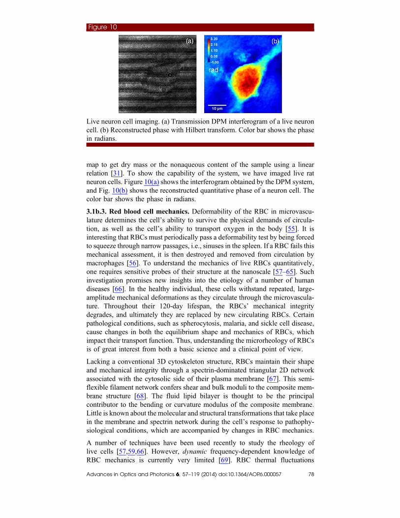
map to get dry mass or the nonaqueous content of the sample using a linearrelation [31]. To show the capability of the system, we have imaged live ratneuron cells. Figure 10(a) shows the interferogram obtained by the DPM system,and Fig. 10(b) shows the reconstructed quantitative phase of a neuron cell. Thecolor bar shows the phase in radians.
3.1b.3. Red blood cell mechanics. Deformability of the RBC in microvascu-lature determines the cell’s ability to survive the physical demands of circula-tion, as well as the cell’s ability to transport oxygen in the body [55]. It isinteresting that RBCs must periodically pass a deformability test by being forcedto squeeze through narrow passages, i.e., sinuses in the spleen. If a RBC fails thismechanical assessment, it is then destroyed and removed from circulation bymacrophages [56]. To understand the mechanics of live RBCs quantitatively,one requires sensitive probes of their structure at the nanoscale [57–65]. Suchinvestigation promises new insights into the etiology of a number of humandiseases [66]. In the healthy individual, these cells withstand repeated, large-amplitude mechanical deformations as they circulate through the microvascula-ture. Throughout their 120-day lifespan, the RBCs’ mechanical integritydegrades, and ultimately they are replaced by new circulating RBCs. Certainpathological conditions, such as spherocytosis, malaria, and sickle cell disease,cause changes in both the equilibrium shape and mechanics of RBCs, whichimpact their transport function. Thus, understanding the microrheology of RBCsis of great interest from both a basic science and a clinical point of view.
Lacking a conventional 3D cytoskeleton structure, RBCs maintain their shapeand mechanical integrity through a spectrin-dominated triangular 2D networkassociated with the cytosolic side of their plasma membrane [67]. This semi-flexible filament network confers shear and bulk moduli to the composite mem-brane structure [68]. The fluid lipid bilayer is thought to be the principalcontributor to the bending or curvature modulus of the composite membrane.Little is known about the molecular and structural transformations that take placein the membrane and spectrin network during the cell’s response to pathophy-siological conditions, which are accompanied by changes in RBC mechanics.
A number of techniques have been used recently to study the rheology oflive cells [57,59,66]. However, dynamic frequency-dependent knowledge ofRBC mechanics is currently very limited [69]. RBC thermal fluctuations
Figure 10
Live neuron cell imaging. (a) Transmission DPM interferogram of a live neuroncell. (b) Reconstructed phase with Hilbert transform. Color bar shows the phasein radians.
Advances in Optics and Photonics 6, 57–119 (2014) doi:10.1364/AOP.6.000057 78
(“flickering”) have been studied for more than a century [70] to better under-stand the interaction between the lipid bilayer and the cytoskeleton [42,71–73].Fluctuations in the phospholipid bilayer and attached spectrin network areknown to be influenced by cytoskeletal defects, stress, and actin–spectrin dis-sociations arising from metabolic activity linked to adenosine-5′-triphosphate(ATP) concentration [59,73–76]. Nevertheless, quantifying these motions is ex-perimentally challenging, and reliable spatial and temporal data are desirable[72,77–79].
In 2010, Park et al. from MIT reported “Measurement of red blood cell mechan-ics during morphological changes” [80]. Blood samples were prepared as de-scribed in Ref. [81]. The RBCs were then placed between coverslips andimaged without additional preparation. The samples were primarily composedof RBCs with the typical discocytic shapes (DCs) but also contained cells withabnormal morphology, which formed spontaneously in the suspension, such asechinocytes (ECs, cells with a spiculated shape) and spherocytes (SCs, cells thathad maintained a roughly spherical shape). By taking into account the free en-ergy contributions of both the bilayer and cytoskeleton, these morphologicalchanges have been successfully modeled [82].
The standard description of a RBC treats the membrane as a flat surface; in real-ity the membrane of a RBC is curved and has the compact topology of a sphere.The Levine group at University of California, Los Angeles, developed a modelthat takes into account this geometrical effect and incorporates the curvature andtopology of a RBC within the fluctuation analysis (for details on this theory, seeRef. [83]). The undulatory dynamics of a RBC is probed experimentally bymeasuring the spatial and temporal correlations of the out-of-plane fluctuationsof the membrane. Theoretically, these correlations can be calculated using theresponse matrix χ and the fluctuation–dissipation theorem [84].
We used the new model of RBC mechanics over the commonly occurringdiscocyte–echinocyte–spherocyte (DC-EC-SC) shape transition [Figs. 11(a),11(c)] [80]. From measurements of dynamic fluctuations on RBC membranes,we extracted the mechanical properties of the composite membrane structure.Subtraction of the instant thickness map from the averaged thickness map pro-vides the instantaneous displacement map of the RBC membranes (Fig. 11, rightcolumn). Over the morphological transition from DC to SC, the RMS amplitudeof equilibrium membrane height fluctuations
ffiffiffiffiffiffiffiffiffiffiffiffihΔh2i
pdecreases progressively
from 134 nm (DCs) to 92 nm (ECs) and 35 nm (SCs), indicating an increase incell stiffness.
To extract the material properties of the RBC, we fit our model to the measuredcorrelation function Λ�ρ; τ� by adjusting the following parameters: the shear μand bulk K moduli of the spectrin network, the bending modulus κ of the lipidbilayer, the viscosities of the cytosol ηc and the surrounding solvent ηs, and theradius of the sphere R. We constrain our fits by setting R to the average radius ofcurvature of the RBC obtained directly from the data and fixing the viscositiesfor all datasets to be ηs � 1.2 mPa · s, ηs � 5.5 mPa · s [77,78]. Finally, for atriangular elastic network we expect μ � λ, so we set K � 2μ [77]. These valuesare in general agreement with those expected for a phospholipid bilayer�5 20� × kBT [79]. The increase in bending modulus suggests changes inthe composition of the lipid membrane. We measured directly the change insurface area of RBCs during the transition from DC to SC morphologies and
Advances in Optics and Photonics 6, 57–119 (2014) doi:10.1364/AOP.6.000057 79

found a 31% decrease in surface area (not accounting for surface area stored influctuations). This surface area decrease must be accompanied by a loss of lipids,via membrane blebbing and microvesiculation. Thus, there is evidence that asignificant change in lipid composition of the RBC bilayer accompanies themorphological changes from DC to EC and SC. It is thought that these changesin lipid composition generate the observed changes in the bending modulus.These data suggest that there are essentially two independent conformationsof the spectrin network: a soft configuration (μ ≅ 7 μNm−1) and a stiff one(μ ≅ 13 μNm−1). Essentially all DCs have the soft configuration, but the mor-phological transition to EC and then SC promotes the transition to the stiff net-work configuration. We propose that the observed morphological changes mustbe accompanied by modifications of the spectrin elasticity, the connectivity ofthe network, or the network’s attachment to the lipid bilayer.
3.1b.4. Imaging of malaria-infected RBCs. Malaria is an infectious diseasecaused by a eukaryotic protist of the genus Plasmodium [67,85]. Malaria is nat-urally transmitted by the bite of a female Anopheles mosquito. This disease iswidespread in tropical and subtropical regions, including parts of the Americas(22 countries), Asia, and Africa. There are approximately 350–500 million casesof malaria per year, killing between 1 and 3 million people, the majority ofwhom are young children in sub-Saharan Africa [85]. In severe cases the diseaseworsens, leading to hallucinations, coma, and death. Five species of thePlasmodium parasite can infect humans; the most serious forms of the diseaseare caused by Plasmodium falciparum. Malaria caused by Plasmodium vivax,Plasmodium ovale, and Plasmodium malariae causes milder disease in humansthat is not generally fatal.
During the intra-erythrocytic (RBC) development, the malaria parasite Plasmo-dium falciparum causes structural, biochemical, and mechanical changes to hostRBCs [86]. Major structural changes include the growing of vacuole of parasites
Figure 11
RBC topography (left column) and instantaneous displacement maps (rightcolumn) for (a) a discocyte, (b) an echinocyte, and (c) a spherocyte, as indicatedby DC, EC, and SC, respectively. Adapted from Park et al., “Measurement ofred blood cell mechanics during morphological changes,” Proc. Natl. Acad. Sci.U.S.A. 107, 6731–6736 (2010) [80] with permission.
Advances in Optics and Photonics 6, 57–119 (2014) doi:10.1364/AOP.6.000057 80

in cytoplasm of host RBCs, loss of cell volume, and the appearance of small,nanoscale protrusions, called “knobs” or “blebs,” on the membrane surface [87].From the biochemical standpoint, a considerable amount of hemoglobin (Hb) isdigested by parasites during intra-erythrocytic development and converted intoinsoluble polymerized forms of heme, known as hemozoin [88,89]. Hemozoin
Figure 12
Topographic images and effective elastic constant maps of Pf -RBCs. (a) and(e) Healthy RBC. (b) and (f) Ring stage. (c) and (g) Trophozoite stage. (d)and (h) Schizont stage. The topographic images in (a)–(d) are the instant thick-ness map of Pf -RBCs. The effective elastic constant maps were calculated fromthe RMS displacement of the thermal membrane fluctuations in the Pf -RBCmembranes. Black arrows indicate the location of P. falciparum, and the grayarrows indicate the location of hemozoin. (Scale bar, 1.5 μm.) Adapted withpermission from Park et al., “Refractive index maps and membrane dynamicsof human red blood cells parasitized by Plasmodium falciparum,” Proc. Natl.Acad. Sci. U.S.A. 105, 13730 (2008) [94]. Copyright 2008 National Academyof Sciences, U.S.A.
Advances in Optics and Photonics 6, 57–119 (2014) doi:10.1364/AOP.6.000057 81

appears as brown crystals in the vacuole of parasites in later maturation stages ofP. falciparum-invaded human RBCs (Pf -RBCs) [67]. Two major mechanicalmodifications are loss of RBC deformability [90–92] and increased cytoadher-ence of the invaded RBC membrane to vascular endothelium and other RBCs[93]. These changes lead to sequestration of RBCs in microvasculature in thelater stages of parasite development, which is linked to vital organ dysfunction insevere malaria. In the earlier stage, where deformability occurs, Pf -RBCscontinue to circulate in the blood stream despite infection.
In 2008, the MIT groups led by Suresh and Feld collaborated on using DPM tostudy the modifications in RBC dynamics produced by the onset and develop-ment of malaria [94]. To investigate morphological changes of Pf -RBCs,we measured the instantaneous thickness profile, h�x; y; t0� of cells [94].Figures 12(a)–12(d) show topographic images of healthy and Pf -RBCs at allstages of development. The effective stiffness map of the cell, ke�x; y�, is ob-tained at each point on the cell, assuming an elastic restoring force associatedwith the membrane:
ke�x; y� � kBT∕hΔh�x; y�2i; (3.1-1)
where kB is the Boltzmann constant, T the absolute temperature, and hΔh�x; y�2ithe mean-squared displacement. Representative ke maps of RBCs at the indi-cated stages of parasite development are shown in Figs. 12(e)–12(g). Themap of instantaneous displacement of cell membrane fluctuation, Δh�x; y; t�,was obtained by subtracting time-averaged cell shape from each thicknessmap in the series.
These results demonstrate a potentially useful avenue for exploiting the nano-scale and quantitative features of QPI for measuring cell membrane fluctuations,which, in turn, can report on the onset and progression of pathological states.
3.2. Reflection Mode
3.2a. Setup
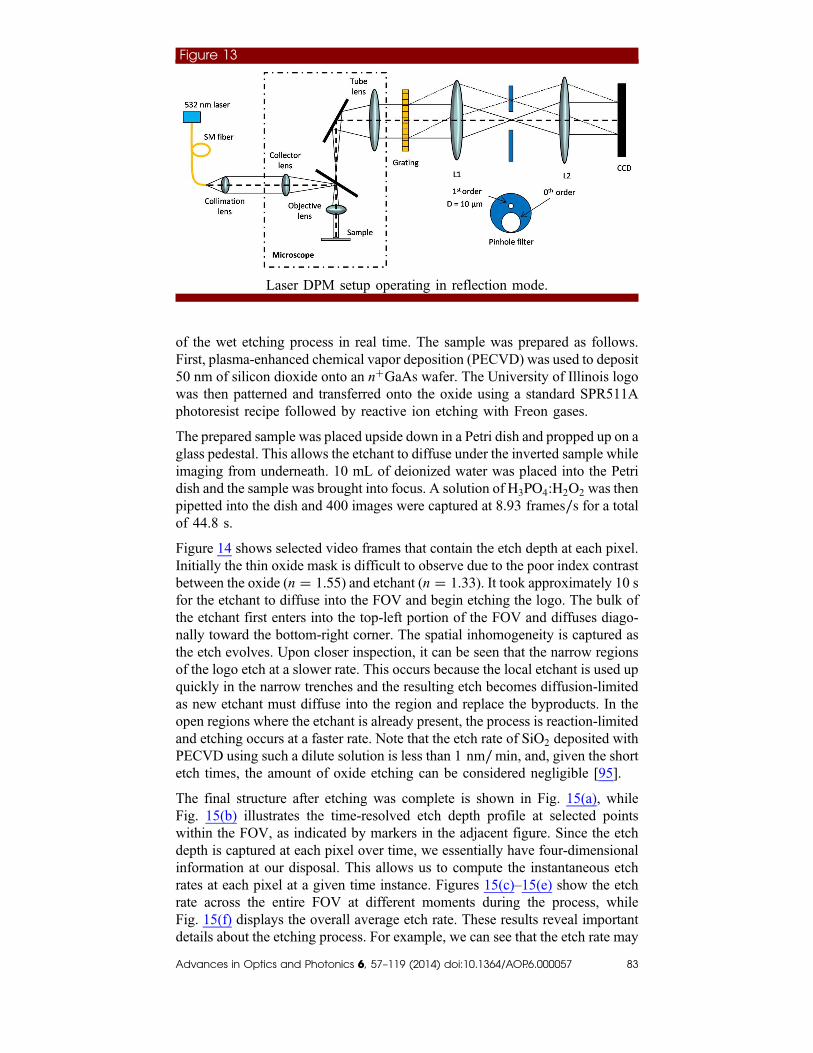
Figure 13 shows a schematic of the laser DPM system operating in reflectionmode (epi-DPM). The prefix epi stands for epi-illumination and stems from thefact that the light is collected from the same side of the sample where it is in-cident. The only difference between reflection and transmission mode is in thelight path within the microscope. In reflection mode, the collimated beam enter-ing the back of the microscope passes through a collector lens and is focusedonto the back focal plane of the objective. The objective lens then creates a col-limated beam in the sample plane. Scattered and unscattered light reflected bythe sample are collected by the objective and again focused in its back focalplane. A beam splitter redirects the light through a tube lens, creating a colli-mated beam containing the image at the output image plane of the microscope.The laser setup at the input and the DPM setup at the output remain unchanged.
3.2b. Applications
3.2b.1. Watching semiconductors etch. The spatial and temporal sensitivitiesdiscussed in Section 2 underscore the capability of epi-DPM to accurately mon-itor dynamics at the nanoscale. To exploit this feature, we captured the dynamics
Advances in Optics and Photonics 6, 57–119 (2014) doi:10.1364/AOP.6.000057 82
of the wet etching process in real time. The sample was prepared as follows.First, plasma-enhanced chemical vapor deposition (PECVD) was used to deposit50 nm of silicon dioxide onto an n�GaAs wafer. The University of Illinois logowas then patterned and transferred onto the oxide using a standard SPR511Aphotoresist recipe followed by reactive ion etching with Freon gases.
The prepared sample was placed upside down in a Petri dish and propped up on aglass pedestal. This allows the etchant to diffuse under the inverted sample whileimaging from underneath. 10 mL of deionized water was placed into the Petridish and the sample was brought into focus. A solution ofH3PO4:H2O2 was thenpipetted into the dish and 400 images were captured at 8.93 frames∕s for a totalof 44.8 s.
Figure 14 shows selected video frames that contain the etch depth at each pixel.Initially the thin oxide mask is difficult to observe due to the poor index contrastbetween the oxide (n � 1.55) and etchant (n � 1.33). It took approximately 10 sfor the etchant to diffuse into the FOV and begin etching the logo. The bulk ofthe etchant first enters into the top-left portion of the FOV and diffuses diago-nally toward the bottom-right corner. The spatial inhomogeneity is captured asthe etch evolves. Upon closer inspection, it can be seen that the narrow regionsof the logo etch at a slower rate. This occurs because the local etchant is used upquickly in the narrow trenches and the resulting etch becomes diffusion-limitedas new etchant must diffuse into the region and replace the byproducts. In theopen regions where the etchant is already present, the process is reaction-limitedand etching occurs at a faster rate. Note that the etch rate of SiO2 deposited withPECVD using such a dilute solution is less than 1 nm∕min, and, given the shortetch times, the amount of oxide etching can be considered negligible [95].
The final structure after etching was complete is shown in Fig. 15(a), whileFig. 15(b) illustrates the time-resolved etch depth profile at selected pointswithin the FOV, as indicated by markers in the adjacent figure. Since the etchdepth is captured at each pixel over time, we essentially have four-dimensionalinformation at our disposal. This allows us to compute the instantaneous etchrates at each pixel at a given time instance. Figures 15(c)–15(e) show the etchrate across the entire FOV at different moments during the process, whileFig. 15(f) displays the overall average etch rate. These results reveal importantdetails about the etching process. For example, we can see that the etch rate may
Figure 13
Laser DPM setup operating in reflection mode.
Advances in Optics and Photonics 6, 57–119 (2014) doi:10.1364/AOP.6.000057 83

vary by several nanometers/second at unmasked points separated by only a fewmicrometers in space at a fixed moment in time or at times separated by only afew seconds at a fixed point in space. These nonuniformities are due to fluctua-tions in the concentration of the etching solution [50].
The epi-DPM technique has demonstrated the ability to monitor wet etchingin situ with nanometer accuracy. This method could potentially be used to createa multi-user cleanroom tool for wet etching that would allow the user to observeall of this information during etching, which could greatly improve the quality ofthe etch as well as the overall yield. Furthermore, the ability to accurately mea-sure these inhomogeneities in real time may provide the means to correct thefabrication on-the-fly by perfusing the etching chamber with an adjustableetchant concentration [50].
3.2b.2. Digital projection photochemical etching. Photochemical etching(PC etching) is a low-cost semiconductor fabrication technique with the ability
Figure 14
Real-time imaging during wet etching of the University of Illinois logo. A5 × objective was used for monitoring the etch, resulting in a FOV of320 μm × 240 μm for each of the images shown. The video was acquired at8.93 frames∕s. It took roughly 10 s for the etchant to diffuse into the FOVand begin etching. Still frames over a 30 s interval from 14–44 s are displayed,showing the dynamics of the etching process. Diffusion of the etchant from thetop-left corner to the bottom-right corner is observed. Adapted from [50].
Advances in Optics and Photonics 6, 57–119 (2014) doi:10.1364/AOP.6.000057 84

to etch structures with gray-scale topography. When light with sufficient energyis absorbed near the surface of a semiconductor material, minority carriers aregenerated that can then diffuse to the surface and act as a catalyst in the etchingprocess. Our lab has recently developed a technique called digital projectionphotochemical etching [96]. Here, we can use a standard classroom projectorto focus a gray-scale image into the sample plane and use light itself as the maskfor etching. This alleviates the need for standard photolithography, which re-quires spin coating photoresist, aligning and exposing, and developing. Withdigital projection PC etching we can etch gray-scale structures that are difficultto fabricate using conventional photolithography and even etch multilevel struc-tures in a single processing step [96]. The color (or wavelength) of the projectorlight, as well its intensity, can be adjusted to control etch rates and even provideboth spatial and material selectivity. The projected pattern may also be adjusteddynamically throughout the etching process.
Figure 16 shows the experimental setup for PC etching, which is integrated intothe DPM workstation [96]. This allows us to measure the dimensions of theetched structures on site in a completely noninvasive manner. This is not pos-sible with scanning electron microscopy (SEM), transmission electron micros-copy, atomic force microscopy, or other similar inspection methods [50,97,98].
Figure 15
Analysis of real-time etching dynamics. (a) Final depth profile after etching wascompleted. (b) Plot of etching depths over time to show variation of depths andetch rates at points indicated in (f). (c)–(e) Etch rates at each pixel across theFOV at frame 150 (16.8 s), frame 250 (28.0 s), and frame 350 (39.2 s). (f) Overalletch rate averaged over the entire etch process. The etch rate may vary by severalnanometers/second over the FOV at any given time, but average out over time.Adapted from [50].
Advances in Optics and Photonics 6, 57–119 (2014) doi:10.1364/AOP.6.000057 85

The bold solid lines represent the light path from the projector, where the maskpattern was focused upon the sample’s surface and aligned using CCD1. Theepi-DPM system was used to measure the height of features on the sample usingCCD2. The light path for epi-DPM is indicated by the dotted lines.
The etch rates for red, green, and blue light at different intensities were deter-mined by projecting a mask pattern with eight 30 μm squares containing graylevels of 32, 64, 96, 128, 160, 192, 224, and 255 for each color and performing a30 s etch [96]. The mean and standard deviation of the measured etch depthinside each square were recorded, and the differential etch rates as a functionof the gray level for each color component were calculated using the recordedetch time and etch depths. The background (dark) etch rate was then measured,which allowed us to determine the absolute etch rate for the different colors andgray levels. These rates were used to compute the etch times required for adesired etch depth (or height) in subsequent etches [96].
To characterize the system, we measured the etch feature resolution and edgeresolution of etched structures, as well as the spatial and temporal noise of theepi-DPM imaging system. To test the resolution of the PC etching process, maskpatterns containing selected portions of the USAF-1951 target with feature sizesranging from 16 to 1.2 μm were created for each color [96]. Figure 17(a) showsan image captured using a 20×, 0.5 NA objective (1.3 μm resolution) andshows the collection of lines taken from a selected portion of the etched target.Figure 17(b) contains a cross section taken along the horizontal lines(2 μm × 10 μm), showing that we are able to clearly resolve the 2 μm featuresfrom the resolution target. Note that three peaks are also faintly visible even at1.4 μm. The etching resolution comprises three components: the diffraction limitof light projected into the sample plane, the diffusion of carriers as a result of thePC etching process (diffusion length for n�GaAs at room temperature is 1.1 μm[99]), and aberrations and imperfections in the optical system. According to
Figure 16
Digital projection PC etching system. Illustration showing the integration of ournewly developed digital projection PC etching and epi-DPM methods. The boldsolid lines represent the light path from the projector, which was focused on thesample and aligned using CCD1. The epi-DPM system was used to measure theheight of features on the sample using CCD2. The light path for epi-DPM isindicated by the dotted lines. Adapted from [96].
Advances in Optics and Photonics 6, 57–119 (2014) doi:10.1364/AOP.6.000057 86

Abbe’s formula, the optical resolution limit for red, green, and blue light usingthe 10×, 0.2 LD objective is 1.9, 1.6, and 1.4 μm, respectively. Further broad-ening in the features is a result of the diffusion of carriers as well as opticalimperfections in the setup. There are also slight discrepancies between the ver-tical and horizontal resolutions, which are due to the rectangular geometry of theRGB subpixels inside the projector. The resolution can be further improved byusing a higher NA objective.
Figure 17(c) contains an epi-DPM height map of our standard control sample, amicropillar, that was etched using our technique. A mask pattern was used withgray levels of 0 and 136 for the pillar and background, respectively. PC etchingwas performed for 60 s, resulting in a mean height of 304.9 nm. It was calibratedto have a 100 μm diameter and a height of 300 nm. Figure 17(d) contains a crosssection of the pillar in Fig. 17(c), showing that the resulting width and heightwere 100 μm and 304.9 nm, respectively. The edge resolution was measured tobe ε � Δx∕Δy � 30, which is due to the diffusion of carriers during the PCetching process. Note that, for a standard isotropic wet etch, the edge resolutionis ε � Δx∕Δy � −1 since there is 1 nm of undercutting per 1 nm of etching. Thisbroadening effect is currently the primary limitation of this new technique, butmay be alleviated using computation photolithography, which prewarps themask pattern in order to achieve more vertical sidewalls.
Figure 17
System characterization. (a) epi-DPM image of horizontal and vertical linesetched using the USAF-1951 resolution target. Image was captured using a20×, NA � 0.5 objective (650 nm lateral resolution). (b) Cross section ofhorizontal lines taken along the dotted line in (c). Based on this resolution test,the etch feature resolution using our PC etching setup is approximately 2 μm.(c) DPM height map of a PC etched micropillar. Mask patterns with graylevels of 0 and 136 were used for the pillar and background, respectively.PC etching was performed for 60 s, resulting in a mean height of 304.9 nm.It was calibrated to have a 100 μm diameter and a height of 300 nm. (d) Crosssection of the pillar in (c) showing the dimensions and edge resolution. Adaptedfrom [96].
Advances in Optics and Photonics 6, 57–119 (2014) doi:10.1364/AOP.6.000057 87

Figure 18(a) shows a height map of stacked cubes that were fabricated in a singleetch step [96]. A projected image with gray levels of 0, 60, and 78 was used forthe mask pattern. PC etching was performed for 33 s, resulting in mean heightsof 0, 50.7, and 101.6 nm. The etched structure was calibrated to have widths of150 and 75 μm with heights of 0, 50, and 100 nm. The corresponding histogramis displayed in Fig. 18(b), which indicates the mean height of each of the threelayers and illustrates the high degree of process control and repeatability.Multiple structures can also be etched simultaneously, as we have illustratedin Fig. 18(c), which contains the surface profile of a microlens array etched usingour technique. The diameters of the microlenses were calibrated to be 100 μmwith a pitch of 120 μm. Figure 18(d) shows a comparison between the projectedpattern and the etched structure. Here, a cross section of the mask pattern isoverlaid with both horizontal and vertical slices from the etched micropillar
Figure 18
Etched structures. (a) DPM height image of stacked cubes. A projected imagewith gray levels of 0, 60, and 78 were used for the mask pattern. PC etchingwas performed for 33 s, resulting in mean heights of 0, 50.7, and 101.6 nm. Itwas calibrated to have widths of 150 and 75 μm with heights of 0, 50, and100 nm. (b) Histogram of image in (c) showing the heights of the threelevels. (c) Topographical reconstruction of a microlens array fabricated usingPC etching. (d) Comparison between s cross section of the projected maskpattern and horizontal and vertical cross sections from an etched microlens.(e) Topographical profile of PC etched Archimedean spiral. Adapted from[50,96].
Advances in Optics and Photonics 6, 57–119 (2014) doi:10.1364/AOP.6.000057 88

image. The mask appears inverted because the dark regions etch most slowly,forming the top of the microlens, while the brighter regions of the mask producethe perimeter of the lens. To further illustrate the strengths of the technique, anArchimedean spiral was fabricated using a continuous gray-scale mask pattern.The gray-level values decreased linearly around the spiral from 96 down to 0.The maximum height and width were calibrated to be 100 nm and 30 μm,respectively. Figure 18(e) shows the surface topography of an etched spiral.Note that this type of structure is very difficult to fabricate using standard photo-lithography. In fact, the spiral would need to be broken up into many discretesteps, each requiring a separate processing step. Note that this structure wasetched in 33 s. To quantify the roughness of the etched structures, the standarddeviations were recorded for the flat regions of the micropillar and multilevelcubes, as reported in Figs. 17(c) and 18(a), respectively. These measurementsshow that the roughness is less than 5 nm for all cases, which is comparableto the roughness of a standard wet etch done under typical cleanroomconditions [96].
Digital projection PC etching is capable of fabricating gray-scale structures thatare otherwise difficult to obtain using standard photolithography and is capableof etching multilevel structures in a single processing step. The etch rates can bedetermined for a given material/etchant combination by performing the etch ratetest described above [96]. The etch feature resolution is between 1.68 and2.38 μm for the three colors as determined by etching selected portions ofthe USAF-1951 target. Furthermore, using this integrated setup, dimensionsof the etched structures can be measured on site in a completely nondestructivemanner.
3.2b.3. Semiconductor wafer defect detection. In-line detection of killer de-fects in patterned wafers has been a grand challenge of the International Tech-nology Roadmap for Semiconductors (ITRS). Currently, the semiconductorindustry is using the 22 nm node technology; thus, detecting defects that aresmaller than 22 nm in size is very critical for semiconductor manufacturersto maximize their yield. To detect defects in 22 nm node wafers, deep ultravioletlasers and high-order harmonic sources have been proposed [100,101]. In fact,the ultimate limiting factor in an imaging system is the signal-to-noise contrast[102]. DPM has very low noise as discussed earlier, so we adapted the epi-DPMsystem to measure both the phase and amplitude of the scattered field from anintentional defect array wafer (IDA) provided by SEMATECH. The IDA waferconsists of 100 μm × 100 μm 2D arrays. Within each array, there are straightlines that are 240 or 120 nm in length and 22 nm wide. In the center of the2D array, there is a printed defect; see Ref. [102] for more details on theIDA wafer and defects. Figure 19 schematically shows different types of defectsfor the IDA wafer, specifically, an isolated dot defect, a perpendicular bridgedefect, and a parallel bridge defect. The defect width can vary in size, whichscales against 22 nm.
For each 2D array, we collect a sequence of interferograms while mechanicallytranslating the wafer with 1 μm stepping size in the line structure direction in theplane parallel to its surface. For each interferogram frame, the phase andamplitude images are retrieved. Since the defect is very small, the various noisesin a single frame can still degrade the defect signal contrast. To improve signalcontrast, we developed a sequence of image postprocessing methods [102,103].After image processing, we stitch all the frames together to produce a stretched
Advances in Optics and Photonics 6, 57–119 (2014) doi:10.1364/AOP.6.000057 89

panoramic image where the noise is significantly decreased and the signal fromthe defect is stabilized. In Figs. 20(a) and 20(b), we show the stretched amplitudeand phase images for a 20 nm × 110 nm parallel bridge defect, respectively, asan example. In both images, the defect can be clearly observed with no falsealarms in the 25 μm × 80 μm FOV. Using the same techniques, other typesof defect were also detected. The minimum defects we detected were 35 nm ×70 nm for an isolated dot defect, 20 nm × 110 nm for a parallel bridge defect,and 20 nm × 110 nm for a vertical bridge defect. These detection results wereconfirmed with SEM.
Figure 19
Illustration of different defect types. (a) An isolated defect, (b) a perpendicularbridge defect, and (c) a parallel bridge defect. Adapted from Zhou et al., “22 nmnode wafer inspection using diffraction phase microscopy and imagepost-processing,” Proc. SPIE 8681, 8610G (2013) [103] with permission fromSPIE.
Figure 20
Stretched image using moving averaging. (a) Stretched amplitude image and(b) stretched phase image. In each stretched image, the location of the defectis marked by a red box. Adapted from Zhou et al., “22 nm node wafer inspectionusing diffraction phase microscopy and image post-processing,” Proc. SPIE8681, 8610G (2013) [103] with permission from SPIE.
Advances in Optics and Photonics 6, 57–119 (2014) doi:10.1364/AOP.6.000057 90

4. White-Light DPM
Because of the high coherence of the laser illumination, laser DPM images sufferfrom speckles, which ultimately degrade the spatial phase sensitivity. We haverecently developed white-light diffraction phase microscopy (wDPM), whichuses white-light illumination and, thus, improves the overall spatiotemporalnoise of the system [54]. DPM imaging systems using white-light illuminationtypically exhibit lower noise than their laser counterparts. This is a result of thelower coherence (both spatially and temporally), which reduces noise mecha-nisms, such as laser speckle. On the other hand, without proper spatial filtering,white-light DPM systems can exhibit aberrations and artifacts, like the halo ef-fect, that are not present in laser DPM systems. Each type of illumination has itsown strengths and weaknesses. Currently, it appears that laser DPM works wellfor material science applications where structural features have large lateral ex-tent and may also have sharp edges, while white light is best suited for biologicalapplications where the features have much smaller lateral extent and aresmoother [104,105].
4.1. Setup
White-light DPM is implemented as an add-on module to a commercial micro-scope (Axio Observer Z1, Zeiss). Figure 21 shows the experimental setup, wherewe employ spatially coherent white-light illumination, obtained from a halogenlamp commonly used in commercial microscopes. In wDPM, the reference beamis created by first closing down the NA of the condenser and then filtering the0th order diffraction beam with a pinhole mask on the spatial light modulator(SLM), which matches with the aperture of the condenser. If the aperture is smallenough, we expect to see a uniform reference beam. In our current configuration,the minimum aperture we can get is NA � 0.09. This results in a reference beamthat is not perfectly uniform and is a low-pass-filtered version of the samplebeam, which in turn can result in halos in the final reconstructed phase images.
Figure 21
wDPM experimental setup.
Advances in Optics and Photonics 6, 57–119 (2014) doi:10.1364/AOP.6.000057 91

This halo effect can be easily removed by reducing the condenser aperture size,however, at the expense of reducing the illumination power. Illumination powerat the sample plane for this NA is 0.16 mW and for fully open condenser(NA � 0.55), it is 5.57 mW. As in DPM, at the image plane of the invertedmicroscope, we place a phase diffraction grating, which generates multiple dif-fraction orders containing full spatial information about the object. The 0th- and1st-order beams are isolated at the Fourier plane generated by lens L1 using aSLM, as shown in Fig. 21. The 0th-order beam is spatially low-pass filtered suchthat only the DC component of the 0th order is passed, whereas the 1st order iscompletely passed. The diameter of the pinhole (zero order mask) at the Fourierplane is 200 μm and the rectangular opening (first order mask) has a size of5 mm × 2 mm. The lens system L1–L2 forms a highly stable Mach–Zehnderinterferometer. The 1st order is thus the imaging field and the 0th order playsthe role of the reference field. Both beams are interfered and generate a spatiallymodulated interference image, which is then captured by a sCMOS camera(Hamamatsu ORCA Flash) at the image plane. The common-path geometrymatches the optical path lengths for the sample and reference arms such thatthe alignment is independent of the wavelength and temporal coherence ofthe illumination source. The quantitative phase image associated with the sampleis retrieved from a single camera recording via a spatial Hilbert transform [41].We assume the live cells as phase objects, which is a common assumption in thefield. This is a valid approximation as, for unstained cells, bright-field imagesshow little to no contrast in intensity. The grating period (9 μm in the presentcase) was set to be smaller than the diffraction-limited spot of the microscopicimaging system at the grating plane. All the lenses are achromatic to minimizechromatic dispersion. Throughout our experiments, the microscope wasequipped with a bright-field 40× (0.75 NA) objective. The L1–L2 lens systemgives an additional magnification of f 2∕f 1 � 2.5, such that the sinusoidal modu-lation of the image is sampled by 6 camera pixels per period.
To characterize the noise stability of our setup, we measured the phase of a timeseries of 256 background images of size 512 × 512, and the phase of a singlebackground phase of the same size at a different spatial position. This back-ground phase was then subtracted from all the previous temporally acquiredphases to correct for any wavefront curvature, which is a constant associatedwith our instrument. Figure 22(a) shows the spatial noise of the wDPM system,obtained by subtracting two reconstructed phase images at two different FOVlocations. The standard deviation of spatial noise in wDPM is a few times lessthan that obtained with DPM [Fig. 22(b)]. A more complete characterization ofthe spatiotemporal noise is obtained by numerically computing the spatial andtemporal power spectrum as follows:
ϕ�k;ω� � α
����Z Z
A
Z∞
−∞δφ�r; t�e−i�ωt−k·r�dtd2r
����2
; (4.1-1)
where α is a normalization factor such that the area under ϕ�k;ω� gives thevariance of the spatiotemporal noise. This power spectral density describesthe contribution to the variance of each temporal and spatial frequency compo-nent. Figures 22(c) and 22(d) illustrate this power spectral density along ωand kx for ky � 0 [Fig. 22(c)] and ky � 2π [Fig. 22(d)]. Our analysis under-scores an important capability: by spatial and temporal bandpass filtering,the measurement noise can be reduced significantly. For example, measuring
Advances in Optics and Photonics 6, 57–119 (2014) doi:10.1364/AOP.6.000057 92

in the frequency range indicated by rectangles A and B in Figs. 22(c) and 22(d)gives optical path length noise levels of 0.11 and 0.07 nm, respectively. Theseremarkably low values are obtained for a spatial bandwidth of π rad∕μm (0.5 μmspatial distance) in both directions and temporal bandwidth of 1 rad∕s, which areeasily achievable in practice. Thus, path-length changes of subangstrom scalecan be measured by spatial and temporal filtering. It should be noted thatthe spatiotemporal filtering is in essence an averaging procedure and, therefore,wDPM’s high acquisition rate can be traded for increased sensitivity.
4.2. Role of Coherence in wDPM
4.2a. Temporal Coherence
The temporal coherence length of white-light systems is typically on the order ofa couple of micrometers, depending on both the source spectrum and the def-inition of coherence length used in the calculation [104,106]. The temporal co-herence can be measured experimentally by first obtaining the spectrum of thesource using a standard spectrometer. The source spectrum for a typical wDPMsystem is shown in Fig. 23(a). The autocorrelation function can then be obtainedthrough a Fourier transform via the Wiener–Khintchine theorem [48,107]. Thetemporal coherence length can then be extracted as shown in Fig. 23(b). Thetemporal coherence length provides a benchmark for the maximum opticalpath-length difference over which we can obtain interference and thus accuratelymeasure height using DPM. Most biological specimens in their typical imaging
Figure 22
Noise stability of wDPM. (a) Spatial noise of wDPM. (b) Spatial noise of laserDPM. (c) and (d) Spatiotemporal power spectral density of wDPM in log scaleat ky � 0 and ky � 2π, respectively; color bars in (c) and (d) arenm2∕��rad∕s� · �rad∕μm�2�. Adapted from [54].
Advances in Optics and Photonics 6, 57–119 (2014) doi:10.1364/AOP.6.000057 93

media exhibit very low index contrast. For example, RBCs in Coulter solutionhave an index contrast of Δn ≈ 0.06 [106]. At a given temporal coherencelength, a lower Δn means that a larger height (i.e., hmax � lc∕Δn �2.0∕0.06 � 33 μm), can be measured. Thus, the temporal coherence of thewDPM light source is at least 1 order of magnitude larger than what is neededto measure typical samples.
4.2b. Spatial Coherence
Our recent studies suggest a connection between the phase reductions in DPMand the degree of spatial coherence of the illumination [104,105]. When theillumination is fully coherent, the correct phase value is retrieved. Otherwise,the phase value will be increasingly underestimated when the degree of spatialcoherence decreases. As pointed out in Refs. [104,105], the measured phasevalue ϕ�x; y� at transverse location �x; y� is related to the “true” phase valueϕo�x; y� through the following relation:
ϕ�x; y� � ϕo�x; y� − arg��exp�iϕo�Ⓥ h��x; y��; (4.2-1)
where h�x; y� is the spatial correlation function of the illumination at the sampleplane. For illustration purposes, we consider two cases. First, when the illumi-nation field on the sample is fully coherent, h�x; y� → c (a constant),ϕ�x; y� → ϕo�x; y� − c. A normalization to zero out the phase value of the back-ground will give ϕ�x; y� → ϕo�x; y�. In this case, the correct phase value isreturned irrespective of the sample’s size and geometries. At the other extreme,when the illumination becomes fully incoherent, i.e., the condenser apertureis infinitely large, h�x; y� → δ�x; y�, we have ϕ�x; y� → ϕo�x; y� −ϕo�x; y� � 0, which establishes that the phase information is lost. Intermediatesbetween these two extremes suggest reductions in the phase values betweenϕo�x; y� and 0. This phase reduction also depends on the sample’s transversedimensions.
Figure 24 shows our measurement of 123 nm micropillars with different radii.We change the amount of spatial correlation by alternating the diameter of thecondenser’s aperture (and hence the NA of the condenser). It can be seen that the
Figure 23
Temporal coherence of the wDPM imaging system. (a) Spectrum of the HAL100 halogen lamp showing the power-equivalent bandwidth approximation. Thecenter wavelength at a color temperature of 3200 K is 574 nm. This wavelengthis used to convert the measured phase to height. (b) Temporal autocorrelationfunction and its envelope obtained via a Hilbert transform. The temporal coher-ence length obtained from the envelope is 2.1 μm. Adapted from [104].
Advances in Optics and Photonics 6, 57–119 (2014) doi:10.1364/AOP.6.000057 94

height measurement converges to the correct value when the illumination be-comes fully coherent irrespective of the sample size. The measured phase valuereduces when the degree of coherence decreases with a decay rate that dependson the sample’s dimensions. Samples with larger sizes tend to have faster decayrates than those of smaller ones.
4.3. Applications
4.3a. Red Blood Cell Membrane Fluctuation Measurement
We have used wDPM for imaging several live cells including RBCs. As wDPMgives low-noise phase images, it can be used for RBC membrane fluctuationmeasurement. For this, we captured 512 images of individual RBCs at50 Hz with a bright-field objective (20×, 0.8 NA). From this time-lapse se-quence, we obtained the average cell thickness map to create a binary maskto avoid the contribution outside the cell. Next we obtained the standarddeviation map inside the masked region. The mean of the standard deviationis the mean cell membrane fluctuation. Figure 25(a) shows a thickness map fromthe sequence. Note that the background outside the RBC is much more uniformthan in the case of laser illumination imaging. Figure 25(b) shows the binarymask obtained from the average map and Fig. 25(c) shows the standarddeviation map, which shows the membrane fluctuations with a mean valueof 30.9 nm for this particular cell. The color bars in Figs. 25(a) and 25(c) showthe cell thickness in micrometers and the membrane fluctuation in nanometers,respectively.
4.3b. QPI of Beating Cardiomyocyte Cell
Studying cardiomyocyte differentiation is important to heart disease researchand drug discovery screening. For functional cardiomyocyte, one indicationof differentiation is the beating of a cell or cell clumps. As the beating ratecan be a few hertz, we need to have a fast QPI method to study the dynamicsquantitatively. We have used our fast wDPM system to image dynamiccardiomyocyte beating at 2.5 Hz. Figure 26(a) shows a quantitative phase image
Figure 24
Measured phase value with respect to different sample size and various valuesof degree of spatial correlation. T. Nguyen, C. Edwards, L. L. Goddard, and G.Popescu are preparing a manuscript to be called “Quantitative phase imagingwith partially coherent illumination,” available from G. Popescu, [email protected].
Advances in Optics and Photonics 6, 57–119 (2014) doi:10.1364/AOP.6.000057 95

of such a cardiomyocyte from the time-lapse sequence acquired at 50 Hz. Thecolor bar shows the phase in radians. Figures 26(b) and 26(c) show line profilesof phase along lines AB and CD, respectively, in Fig. 26(a) at different times.The spikes are due to cell beating, and time difference between two spikesdetermines the beating period.
4.3c. Cell Growth Study
White-light DPM is built as an add-on module to a commercial bright-field mi-croscope that is equipped with an incubator and heating stage for imaging live
Figure 25
RBC membrane fluctuation measurement with wDPM. (a) RBC thickness map.(b) Generated binary mask. (c) Standard deviation map. Color bar in (a) showsthickness in micrometers and that in (c) shows standard deviation in nanometers.The mean of the standard deviation in the masked area is 30.9 nm.
Figure 26
Beating cardiomyocyte imaging with wDPM. (a) Phase image. (b) Phase profilealong line AB. (c) Phase profile along line CD. Color bar shows phase in radians.
Advances in Optics and Photonics 6, 57–119 (2014) doi:10.1364/AOP.6.000057 96
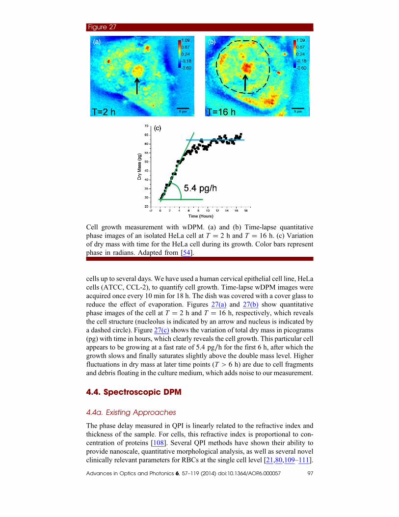
cells up to several days. We have used a human cervical epithelial cell line, HeLacells (ATCC, CCL-2), to quantify cell growth. Time-lapse wDPM images wereacquired once every 10 min for 18 h. The dish was covered with a cover glass toreduce the effect of evaporation. Figures 27(a) and 27(b) show quantitativephase images of the cell at T � 2 h and T � 16 h, respectively, which revealsthe cell structure (nucleolus is indicated by an arrow and nucleus is indicated bya dashed circle). Figure 27(c) shows the variation of total dry mass in picograms(pg) with time in hours, which clearly reveals the cell growth. This particular cellappears to be growing at a fast rate of 5.4 pg∕h for the first 6 h, after which thegrowth slows and finally saturates slightly above the double mass level. Higherfluctuations in dry mass at later time points (T > 6 h) are due to cell fragmentsand debris floating in the culture medium, which adds noise to our measurement.
4.4. Spectroscopic DPM
4.4a. Existing Approaches
The phase delay measured in QPI is linearly related to the refractive index andthickness of the sample. For cells, this refractive index is proportional to con-centration of proteins [108]. Several QPI methods have shown their ability toprovide nanoscale, quantitative morphological analysis, as well as several novelclinically relevant parameters for RBCs at the single cell level [21,80,109–111].
Figure 27
Cell growth measurement with wDPM. (a) and (b) Time-lapse quantitativephase images of an isolated HeLa cell at T � 2 h and T � 16 h. (c) Variationof dry mass with time for the HeLa cell during its growth. Color bars representphase in radians. Adapted from [54].
Advances in Optics and Photonics 6, 57–119 (2014) doi:10.1364/AOP.6.000057 97

However, since the optical phase shift is a function of both thickness and re-fractive index, more than one measurement is needed to decouple the thicknessand refractive index of the cells. Existing approaches to solve this problem in-clude measuring the phase shift with respect to two different media with differ-ent refractive indices or measuring quantitative phases at different light colors.The former approach requires the cells be kept in place as the media is changedand thus may not be well suited for clinical measurements [112,113]. Park et al.[114] developed spectroscopic phase microscopy (SPM), which is essentiallyDPM at different wavelengths using several BPFs with white-light illumination.Imaging the quantitative phase maps at different wavelengths helps differentiateamong molecules. This instrument has many potential applications, one ofwhich is quantifying isomeric shifts in Hb (oxy- and deoxy-Hb) when exposedto different oxygen pressures. Binding of oxygen to Hb proteins causes confor-mational changes that result in significant differences in dispersion. Thus, anSPM instrument may provide a valuable tool for the better understanding ofoxygen transport by RBCs. Similarly, Fu et al. [115] developed a dual-wavelength quantitative phase microscope, also based on DPM, using two in-dependent laser sources at different wavelengths. Further, quantitative phasespectroscopy (QPS) was recently proposed by using a supercontinuum laser andan acousto-optic tunable filter; it is capable of measuring the wavelength-dependent refractive index of microscopic volumes [116]. Quantitative phaseimages of semitransparent samples are recovered at each wavelength usingoff-axis interferometry and are processed to recover relative and absolutedispersion measurements.
4.4b. Spectroscopic DPM with White Light
One limitation of most of the above methods is that they require mechanicalmoving components in the system: switching of the filters [114], or filter wheel[106] or manual switching of the media [113]. Although the QPS method allowsquantitative phase imaging at several wavelengths with high spectral resolutionacross the visible range, it requires an expensive supercontinuum laser lightsource and a tunable filter. In this section, we present a new method, spectro-scopic diffraction phase microscopy (sDPM), that can measure quantitative cell-induced phase shifts at several wavelengths [117]. Spectroscopic DPM requiresno moving parts in the system, and the spectroscopic measurement can be per-formed simply by changing PowerPoint slides projected on a projector SLM,which can be done automatically with full digital control. The sDPM methodis demonstrated by measuring the dispersion of microsphere beads andhemoglobin-induced dispersion in RBCs.
The sDPM setup is similar to that of wDPM except for the filter mask projectedon the SLM, as shown in Fig. 28. The key observation is that, because of thediffraction grating, different wavelengths are diffracted at different diffractionangles, and thus the 1st order is dispersed at the Fourier plane. Lens L2 thenfocuses the dispersed signal back to the same point in the image plane. Basedon this observation, in order to select the wavelengths, we project a pinhole (acircular mask on the SLM) at different positions in the 1st order, as depicted ininset a in Fig. 28. Of course, the 0th order is not dispersed in wavelengths, i.e., itmaintains a white color. The lens system L1–L2 forms a highly stable Mach–Zehnder interferometer. The filtered 1st order is used as the reference beam,and the 0th order is the imaging field. The two beams are interfered on a
Advances in Optics and Photonics 6, 57–119 (2014) doi:10.1364/AOP.6.000057 98
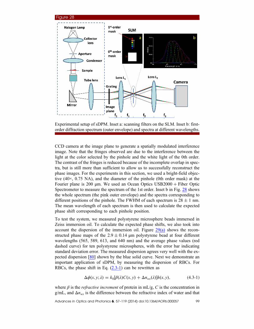
CCD camera at the image plane to generate a spatially modulated interferenceimage. Note that the fringes observed are due to the interference between thelight at the color selected by the pinhole and the white light of the 0th order.The contrast of the fringes is reduced because of the incomplete overlap in spec-tra, but is still more than sufficient to allow us to successfully reconstruct thephase images. For the experiments in this section, we used a bright-field objec-tive (40×, 0.75 NA), and the diameter of the pinhole (0th order mask) at theFourier plane is 200 μm. We used an Ocean Optics USB2000� Fiber OpticSpectrometer to measure the spectrum of the 1st order. Inset b in Fig. 28 showsthe whole spectrum (the pink outer envelope) and the spectra corresponding todifferent positions of the pinhole. The FWHM of each spectrum is 28� 1 nm.The mean wavelength of each spectrum is then used to calculate the expectedphase shift corresponding to each pinhole position.
To test the system, we measured polystyrene microsphere beads immersed inZeiss immersion oil. To calculate the expected phase shifts, we also took intoaccount the dispersion of the immersion oil. Figure 29(a) shows the recon-structed phase maps of the 2.9� 0.14 μm polystyrene bead at four differentwavelengths (565, 589, 613, and 640 nm) and the average phase values (reddashed curve) for ten polystyrene microspheres, with the error bar indicatingstandard deviation error. The measured dispersion agrees very well with the ex-pected dispersion [80] shown by the blue solid curve. Next we demonstrate animportant application of sDPM, by measuring the dispersion of RBCs. ForRBCs, the phase shift in Eq. (2.3-1) can be rewritten as
Δϕ�x; y; λ� � k0�β�λ�C�x; y� � Δnws�λ��h�x; y�; (4.3-1)
where β is the refractive increment of protein in mL/g, C is the concentration ing/mL, and Δnws is the difference between the refractive index of water and that
Figure 28
Experimental setup of sDPM. Inset a: scanning filters on the SLM. Inset b: first-order diffraction spectrum (outer envelope) and spectra at different wavelengths.
Advances in Optics and Photonics 6, 57–119 (2014) doi:10.1364/AOP.6.000057 99

of the surrounding media. Figure 29(b) presents phase maps of an RBC at thesame four different wavelengths and the dispersion curve associated with thesemeasurements. We use C � 32 g∕dL and data for the refractive increment βfrom the literature [118] to compute the expected phase shift of a 2 μm thickRBC. For the measured data, we normalized the phase values of each cell to themean of the end points of the measured dispersion to remove the errors due tovariations in RBC thickness values; different thicknesses shift this curve onlyvertically. Then the phase value at each wavelength was averaged over 10 cells.
In summary, by adding simple optics, we can convert a commercial microscopeto a quantitative phase spectroscopy instrument, sDPM, capable of measuringquantitative phase maps at multiple wavelengths. This method has the advantageof using existing microscopes with minimal changes, and the selection of thewavelength can be done automatically with full digital control. This techniquewill be very useful for studying various blood disorders.
5. Real-Time DPM
We demonstrate a real time off-axis QPI system that is capable of reconstructingand displaying phase images in real time at 40 frames∕s. This performance isachieved by combining high-speed single-shot off-axis diffraction phase micros-copies with a reconstruction algorithm based on NVIDIA’s CUDA parallel com-puting architecture. The developed software method can be used with both laserand white-light diffraction phase microscopies. For the demonstration in thissection, we chose to use wDPM. As for the applications, we show, for the firsttime to our knowledge, real-time analysis of blood smears. While the slide isscanned throughout the FOV, the instrument analyzes and displays several bloodparameters at the single cell level and in the end performs population statistics.Even though automatic blood analyzers, such as flow cytometers and impedancecounters, have been proven to be effective tools for physicians and researchers,
Figure 29
Reconstructed phase maps in radians at different wavelengths and dispersioncurves of microbeads and red blood cells. (a) 3 μm beads in Zeiss immersionoil. (b) Red blood cell. Measured (dashed line) and expected (solid line)dispersion curves. The error bars indicate standard deviation (N � 10). Adaptedfrom [117].
Advances in Optics and Photonics 6, 57–119 (2014) doi:10.1364/AOP.6.000057 100

they provide limited information on the detailed morphology of individual cells,and merely alert the operator to manually examine a blood smear by raising flagswhen abnormalities are detected. Our method provides the same information onRBCs as is provided by current automatic analyzers, while giving additional,currently unavailable parameters on the 2D and 3D morphology of individualRBCs.
5.1. Real-Time Phase Reconstruction Using GraphicsProcessing Units
As discussed earlier, the phase images can be reconstructed using Hilbert trans-form. However, the reconstructed phase images often have phase wrappingissues and a phase unwrapping process needs to be used to get the final phaseimages. There are two main types of phase unwrapping algorithm: path-following algorithms and the minimum-norm algorithms [119]. A classic path-following algorithm, Goldstein’s algorithm, achieves the fastest performance;however, its implementation in sequential code is still slow and far from meetingreal-time requirements. For example, Goldstein’s algorithm implemented inC-code takes about 150 ms to unwrap a 1024 × 1024 pixels modulo-2π imagefrom DPM [42], in addition to about 300 ms to extract the modulo-2π imagefrom the raw DPM data.
In this section, we demonstrate real-time off-axis QPI by developing a phasereconstruction algorithm based on NVIDIA’s CUDA programming model. Inthe CUDA programming model, graphics processing units (GPUs) are usedas computation devices and operate as coprocessors to the central processingunit (CPU) [120]. These computation devices perform computationally intensiveparts in parallel. Hundreds of processor cores operate together to process thesame instruction but on different segments of the dataset in the application. Pre-vious work on using GPUs for 2D phase unwrapping include Karasev et al.[121] and Mistry et al. [122]. The former implemented a weighted least-squaresalgorithm for interferometric synthetic aperture radar (IFSAR) data, and the lat-ter implemented a minimum Lp norm phase unwrap algorithm for an opticalquadrature microscopy system. Karasev et al. reported a 35× speed-up inweighted least-square 2D phase unwrapping, but it still takes 5.69 s to unwrapone 1024 × 1024 pixel image. In the latter work, it reportedly takes 2.8 s tounwrap one 640 × 480 pixel image.
Figure 30 illustrates a flow chart of the procedure to reconstruct the phase im-ages from the interferograms. The phase extraction module performs the Hilberttransform, which is equivalent to the following steps: perform Fourier transformof the interferogram; shift the first-order peak to the center and filter everythingelse out; and then perform an inverse Fourier transform and arctangent opera-tion. We chose the Goldstein algorithm for phase unwrapping since it is fast andperforms well with our images. In this section, we present the implementation ofthe phase reconstruction algorithm on a GPU. To further utilize the GPU’spower, we developed a program that can process multiple images simultane-ously. This will be useful for streaming-type applications.
5.1a. Phase Extraction Module
This module to extract phase information from interferogram images involvesFourier transforms, point-wise matrix multiplications (for filtering), shifting of
Advances in Optics and Photonics 6, 57–119 (2014) doi:10.1364/AOP.6.000057 101

matrix entries, and computing the argument of the complex number at each pixelof the image. For Fourier transforms, we use the CUFFT library developed byNVIDIA [123]. In the Fourier domain, the filtering part is simply point-wisematrix multiplication and the fast Fourier transform shifting, circular shifting,and the arctangent operation are all very straightforward for parallel implemen-tation since there are no dependencies between data points. These operations areimplemented using a thread-per-pixel model that assigns a thread to compute foreach pixel of the image.
5.1b. CUDA-Based Phase Unwrapping Algorithm
The first step in the Goldstein algorithm, residue identification, is done on apixel-by-pixel basis; each thread computes an integral over a closed four-pixelloop to decide whether the pixel at the top-left corner of the loop is a residue ornot. This information is then stored in an array of byte type, called a bitflag array[51], to mark the pixel as a positive/negative residue. Next, the branch cut algo-rithm includes processes of enlarging and searching over a search box on theimage to connect the residue to balance out the charge. This process requiresknowledge about other residues it encounters during the search, such as whetherit has been visited by other searches or it has already been connected to someother residues. Thus, this process is very difficult to parallelize. One can imple-ment this process sequentially in the host code, but this requires data copiesbetween the GPU device’s memory and the host memory, which introducesa significant time delay. To avoid this back-and-forth copying, for each imagewe use one thread to perform this step. Furthermore, instead of scanning over thewhole image to search for residues, as in the original Goldstein algorithm, weperform the search on the residue lists stored in the residue identification step.
Figure 30
Phase reconstruction procedure of an off-axis quantitative phase imagingsystem.
Advances in Optics and Photonics 6, 57–119 (2014) doi:10.1364/AOP.6.000057 102
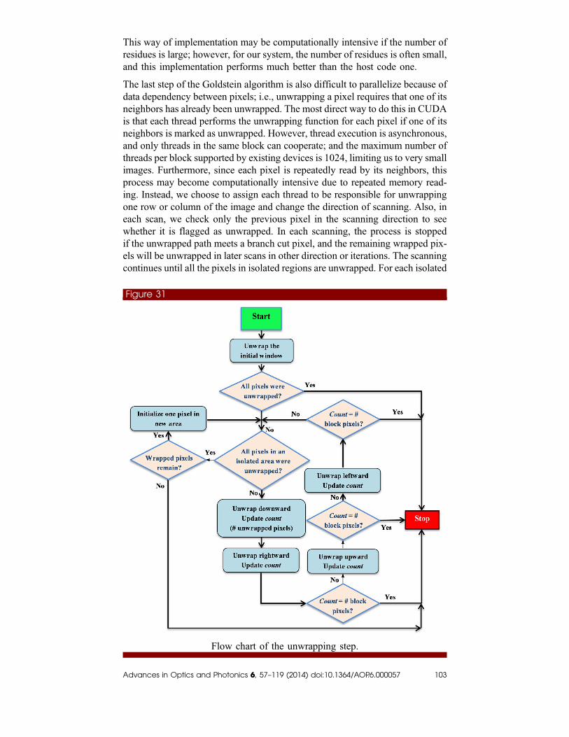
This way of implementation may be computationally intensive if the number ofresidues is large; however, for our system, the number of residues is often small,and this implementation performs much better than the host code one.
The last step of the Goldstein algorithm is also difficult to parallelize because ofdata dependency between pixels; i.e., unwrapping a pixel requires that one of itsneighbors has already been unwrapped. The most direct way to do this in CUDAis that each thread performs the unwrapping function for each pixel if one of itsneighbors is marked as unwrapped. However, thread execution is asynchronous,and only threads in the same block can cooperate; and the maximum number ofthreads per block supported by existing devices is 1024, limiting us to very smallimages. Furthermore, since each pixel is repeatedly read by its neighbors, thisprocess may become computationally intensive due to repeated memory read-ing. Instead, we choose to assign each thread to be responsible for unwrappingone row or column of the image and change the direction of scanning. Also, ineach scan, we check only the previous pixel in the scanning direction to seewhether it is flagged as unwrapped. In each scanning, the process is stoppedif the unwrapped path meets a branch cut pixel, and the remaining wrapped pix-els will be unwrapped in later scans in other direction or iterations. The scanningcontinues until all the pixels in isolated regions are unwrapped. For each isolated
Figure 31
Flow chart of the unwrapping step.
Advances in Optics and Photonics 6, 57–119 (2014) doi:10.1364/AOP.6.000057 103

region, we first initialize a pixel in the region and repeat the above process. Thisinitial pixel was chosen in the scanning process of the previous isolated region.Figure 31 presents the flow chart of this last step.
5.1c. Performance Results
We tested the algorithm on a Windows machine with Intel Core i5 CPU withclock rate of 3.2 GHz and 8 GB RAM memory. We use NVIDIA GeForce GTX470M GPU that supports CUDA programming.
Table 2 compares the performances of the developed parallel algorithm with thesequential C-code-based implementation [119]. The results shown were aver-aged over 20 images for each image size. In the case of processing multipleimage frames simultaneously, for the sequential C-code program the run timesimply scales linearly with the number of frames. For GPU implementation, thetotal run time includes time for the memory copy of interferogram from host todevice and also a memory copy of the output unwrapped image from device tohost. Clearly, the GPU implementation performs much faster than the sequen-tial one.
5.2. Applications
In clinical settings, existing technologies used for blood testing, such as imped-ance counters and flow cytometers, are often accurate and offer high throughput.However, they are expensive and provide only limited information about theRBCs, such as the mean corpuscular volume (MCV) and hemoglobin concen-tration. Based on these parameters, the instrument flags abnormalities, and,usually, a trained physician is required to visually assesses the stained bloodsmears through the light microscope for further evaluation on the detailed mor-phology of the RBCs. The process of staining requires dedicated infrastructure,i.e., specialized instruments, dyes, and trained personnel [124]. These require-ments have prevented blood testing from becoming universally available, espe-cially in economically challenged countries and rural areas. To address this
Table 2. CUDA Implementation versus C-Based Sequential Implementation
PhaseExtraction
(ms)
ResidueIdentification
(ms)
Branch CutPlacement
(ms)Unwrap(ms)
Total(ms)Image Size CPU/GPU
1024 × 1024
1 frameCPU 317.42 43.42 6.74 89.32 460.7GPU 5.05 0.58 1.125 10.014 24.55
Speedupfactor
62.86 74.19 5.99 8.92 18.77
1024 × 1024
10 framesCPU 3174.2 434.2 67.4 893.2 4607.4GPU 40.486 5.55 1.128 45.285 111.1
Speedupfactor
78.4 78.19 59.71 19.72 41.47
512 × 512 1frame
CPU 71 11 5 16 105GPU 2.18 0.2 0.02 1.87 8
Speedupfactor
32.61 55.84 250 8.55 13.13
512 × 512
10 framesCPU 710 110 50 160 1050GPU 11.57 1.4 0.02 6.722 26
Speedupfactor
61.37 78.57 2500 23.8 40.38
Advances in Optics and Photonics 6, 57–119 (2014) doi:10.1364/AOP.6.000057 104

problem, researchers have developed several solutions to decrease the cost of theimaging instruments by utilizing existing and popular commercial devices, suchas cell phone cameras, and converting them into disposable accessories[125,126]. However, so far, these instruments provide only qualitative informa-tion and require further analysis by trained staff. Of course, the data can be trans-mitted for remote diagnosis, a principle known as telepathology [127]; however,the output data usually is a large volume of images, and transferring a largedataset may be difficult in economically challenged areas.
Instead of focusing on reducing the instrument cost, we developed a highly sen-sitive blood testing instrument that operates in real time and outputs data thatcontains quantitative analysis, providing rich diagnostic information [128]. Themeasured phase image provides nanometer-scale information about the RBCprofile, which translates into highly sensitive measurement of the volumeand morphology. Thousands of images are then analyzed, and the outputsare in the form of arrays of numbers that characterize the morphology and dy-namics of RBCs. Therefore, the output data size is small (kilobytes of memory)and can be easily transmitted for remote diagnosis. We combine the single-shothighly sensitive imaging method (wDPM) with parallel image processing algo-rithms to extract morphological parameters at the single cell level from the entireFOV (1 megapixel) in less than 25 ms and to analyze an entire blood smear in afew minutes. Thus, since the blood necessary for this test can be obtained via asimple finger prick, we envision that our instrument can operate in economicallychallenging areas where access to clinical settings is limited.
Figure 32 shows the overall architecture of our system. At the beginning of eachmeasurement, a background subtraction is necessary to remove the effects ofinherent dust and aberrations along the optical path. Since we want to have2D and 3D morphological information on each single cell, the phase
Figure 32
Overview of the blood-testing instrument. The white-light diffraction phase mi-croscope is used as the imaging system. Different CUDA modules performphase reconstruction and image analysis to calculate several morphologicalparameters of individual RBCs. The output information is in the form of arraysof numbers and can be easily transmitted for remote diagnosis.
Advances in Optics and Photonics 6, 57–119 (2014) doi:10.1364/AOP.6.000057 105

reconstruction algorithm is followed by cell segmentation and analysis. Thismodule is responsible for isolating and labeling each individual cell in theFOV and then calculating various morphological parameters associated witheach cell while the blood smear is scanned through the FOV.
5.2a. Single Cell Parameters Computed in Real Time
First, the projected area (PA) parameter can be easily obtained by multiplyingthe number of pixels of each cell by the camera pixel area and dividing by themagnification of the imaging system. The PA then can be used to calculate theequivalent circular diameter, assuming that the projected area of a RBC is acircular disk. As we know, the measured phase shift is proportional to the thick-ness and refractive index of the cells. If we know the refractive index of RBCs,the phase map ϕ�x; y� can be converted to a height map h�x; y� ash�x; y� � λϕ�x; y�∕2πΔn, where λ is the wavelength of the light source andΔn � nc − n0 is the refractive index difference between RBCs and the surround-ing medium. Once the height information is retrieved, the volume of each cell iscalculated by integrating the height map over the PA as V � RR
h�x; y�dxdy. Tocalculate the surface area, we use Monge parameterization [129], where thecontribution of each pixel element dA can be calculated as dA �Parea�1� h2x � h2y�1∕2, where Parea is the area of 1 pixel, and hx and hy arethe gradients along the x and y directions, respectively. The surface area of eachcell is then the sum of all the area elements dA of all the pixels within the cellboundary and the PA, as the cell lays flat on the coverslip. The volume and thesurface area determine the shape of the cell; from these two parameters, we cancalculate several morphological parameters characterizing the RBCs, such assphericity and minimum cylindrical diameter (MCD), determined as importantparameters by Canham and Burton [130]. The sphericity index is calculated asψ � 4.84 V2∕3∕SA. The MCD predicts the smallest capillary diameter that aRBC with that given shape can squeeze through and, thus, is clinically signifi-cant. Furthermore, we are able to calculate many other independent parameters[106], including: perimeter, circular diameter, eccentricity, minimum, maxi-mum, and mean thickness, circularity, integrated density, kurtosis, skewness,and variance. Therefore, our method provides rich and detailed informationat the single cell level and at the population level with several thousands of cellsper patient. This capability allows us to come up with several analysis tools andlook at different sets of parameters and their relations to study and characterizeabnormal cells and diseases that would otherwise be difficult or impossible todetect in an impedance counter or manually in a smear.
5.2b. Cell Segmentation and Connected Component Labeling
To calculate single cell parameters, we have to be able to isolate and label differ-ent cells in the FOV. To do that, for each image, we will have a label map ini-tiated with all zeroes at all pixel positions, apply a threshold to the reconstructedphase map to separate objects of interest from the background, update the labelmap, and label each non-background pixel with a label equal to the pixel index inthe image; this label is regarded as its initial reference. At the same time, wecalculate the volume and surface area contributions, and assign a pixel count(equal to 1, to be used to calculate PA, average height, and other parameterslater) at each and every non-background pixel simultaneously.
Advances in Optics and Photonics 6, 57–119 (2014) doi:10.1364/AOP.6.000057 106
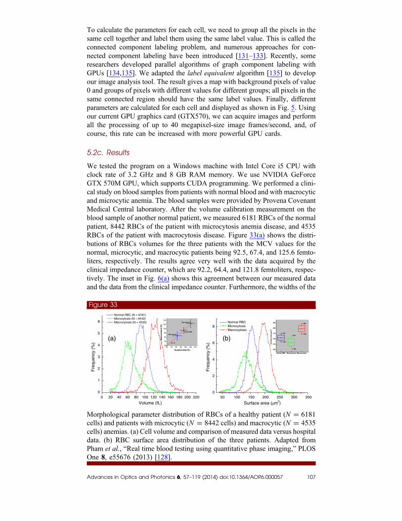
To calculate the parameters for each cell, we need to group all the pixels in thesame cell together and label them using the same label value. This is called theconnected component labeling problem, and numerous approaches for con-nected component labeling have been introduced [131–133]. Recently, someresearchers developed parallel algorithms of graph component labeling withGPUs [134,135]. We adapted the label equivalent algorithm [135] to developour image analysis tool. The result gives a map with background pixels of value0 and groups of pixels with different values for different groups; all pixels in thesame connected region should have the same label values. Finally, differentparameters are calculated for each cell and displayed as shown in Fig. 5. Usingour current GPU graphics card (GTX570), we can acquire images and performall the processing of up to 40 megapixel-size image frames/second, and, ofcourse, this rate can be increased with more powerful GPU cards.
5.2c. Results
We tested the program on a Windows machine with Intel Core i5 CPU withclock rate of 3.2 GHz and 8 GB RAM memory. We use NVIDIA GeForceGTX 570M GPU, which supports CUDA programming. We performed a clini-cal study on blood samples from patients with normal blood and with macrocyticand microcytic anemia. The blood samples were provided by Provena CovenantMedical Central laboratory. After the volume calibration measurement on theblood sample of another normal patient, we measured 6181 RBCs of the normalpatient, 8442 RBCs of the patient with microcytosis anemia disease, and 4535RBCs of the patient with macrocytosis disease. Figure 33(a) shows the distri-butions of RBCs volumes for the three patients with the MCV values for thenormal, microcytic, and macrocytic patients being 92.5, 67.4, and 125.6 femto-liters, respectively. The results agree very well with the data acquired by theclinical impedance counter, which are 92.2, 64.4, and 121.8 femtoliters, respec-tively. The inset in Fig. 6(a) shows this agreement between our measured dataand the data from the clinical impedance counter. Furthermore, the widths of the
Figure 33
0
1
2
3
4
5
6
20 40 60 80 100 120 14020
40
60
80
100
120
140
Fre
quen
cy (
%)
Volume (fL)
Normal RBC (N = 6181) Microcytosis (N = 8442) Macrocytosis (N = 4535)
Mea
sure
men
t (f
L)
Hospital data (fL)
Normal RBC
Microcytosis
Macrocytosis
y = x
0 20 40 60 80 100 120 140 160 180 200 220 50 100 150 200 250 300 3500
2
4
6
8
1 SD
-1 SD
1 SD
-1 SD
1 SD
-1 SD
Fre
quen
cy (
%)
Surface area (µm2)
Normal RBC Microcytosis Macrocytosis
Normal RBC Microcytosis Macrocytosis
100
125
150
175
200
225
Su
rfac
e ar
ea (
µm2 )
(a) (b)
Morphological parameter distribution of RBCs of a healthy patient (N � 6181
cells) and patients with microcytic (N � 8442 cells) and macrocytic (N � 4535
cells) anemias. (a) Cell volume and comparison of measured data versus hospitaldata. (b) RBC surface area distribution of the three patients. Adapted fromPham et al., “Real time blood testing using quantitative phase imaging,” PLOSOne 8, e55676 (2013) [128].
Advances in Optics and Photonics 6, 57–119 (2014) doi:10.1364/AOP.6.000057 107

red blood cell distribution (RDW) curves also show great agreement betweenour measured data and that from the Beckman–Coulter machine. This RDWvalue is also an important diagnostic parameter. An elevated RDW (red bloodcells of unequal sizes) is known as anisocytosis. Specifically, the RDW valuesfor normal, microcytic, and macrocytic patients are 16.5%, 30.1%, and 15.6%,respectively, which agree very well with the data from the clinical analyzers(15%, 29.7%, and 13.9%, respectively). Figure 33(b) shows, as expected, thatthe cell surface area is increasing from microcytic, to normal, to macrocyticcells. The inset in Fig. 33(b) shows statistical information at population levelof each patient with a range to indicate standard deviation and boxes to illustrateinterquartile range.
In addition to parameters that the automatic analyzers provide, our system is ableto provide several more 2D and 3D morphological parameters in great detail.Figures 34(a) and 34(b) show some other example distributions of the sphericityindex and MCD, respectively, with the insets showing the statistical informationfor each patient. Current automated analyzers cannot provide these parameters.Thus, a pathologist has to manually examine a smear to confirm diagnosis ofspherocytosis if the results from automatic analyzers raise a warning flag of thatpossibility. Our system provides this diagnosis in great detail using the spheric-ity index for each and every single cell.
6. Summary and Discussion
DPM has enabled numerous applications in both materials and life sciences.DPM’s off-axis geometry allows single-shot measurements and the study ofrapid phenomena. More importantly, DPM is a common-path technique, whichensures phase stability against noise and, thus, high temporal phase sensitivity.Because it uses a diffraction grating at the image plane, specific sampling con-ditions must be satisfied to preserve the diffraction-limited resolution. Section 2establishes quantitative constraints on the grating period versus diffraction spotsize at the image plane, as well as pixel size versus grating period at thecamera plane.
Figure 34
0
2
4
6
8
10
12
1 SD
-1 SD
1 SD
-1 SD
1 SD
-1 SD
Fre
quen
cy (
%)
Sphericity
Normal RBC Microcytosis Macrocytosis
Normal RBC Microcytosis Macrocytosis0.5
0.6
0.7
Sp
her
icit
y
0.4 0.5 0.6 0.7 0.8 0.9 1.0 1.5 2.0 2.5 3.0 3.5 4.0 4.50
2
4
6
8
10
1 SD
-1 SD1 SD
-1 SD
1 SD
-1 SD
Fre
quen
cy (
%)
MCD (µm)
Normal RBC Microcytosis Macrocytosis
Normal RBC Microcytosis Macrocytosis1.5
2.0
2.5
3.0
MC
D (
µm)
(b)(a)
Examples of output distributions of other morphological parameters. (a)Sphericity index. (b) MCD. Adapted from Pham et al., “Real time blood testingusing quantitative phase imaging,” PLOS One 8, e55676 (2013) [128].
Advances in Optics and Photonics 6, 57–119 (2014) doi:10.1364/AOP.6.000057 108

Originally, DPM was developed with laser illumination (Section 3), but later theoperation principle was extended to white light (Section 4). Laser illuminationhas a clear advantage in terms of brightness. For example, laser light can becoupled into a single-mode fiber and further collimated, which can easily ensurethe high spatial coherence necessary for accurate phase measurements. Whenusing white light, on the other hand, speckles are significantly averaged,improving the spatial phase sensitivity. Furthermore, this illumination modecan be achieved by using existing microscopes without changing their typicalillumination. Thus, common halogen lamps can be used, provided the condenseraperture is reduced to ensure spatial coherence. However, these sources are spa-tially extended, and, thus, achieving high spatial coherence can be achieved onlywith significant loss in power.
We described laser DPM in both transmission and reflection geometries. Thetransillumination reveals details about transparent structures, such as unstainedcells and thin slices of tissues. More recently, the DPM principle has beenextended to epi-illumination to study materials that are opaque in the visiblerange of the spectrum, including silicon wafers and semiconductor structures.Monitoring in real-time topography using manufacturing processes is an excit-ing new field of application for DPM and QPI in general.
Finally, Section 5 describes how recent advances in computing, especially usingGPUs, allow performance of previously impossible tasks, such as real-timequantitative phase imaging of dynamic samples. It is now possible to analyzeimages and extract quantitative information in real time. This trend is likely tocontinue, eliminating one day the need to save the images in the first place.Transforming the microscope into an instrument that outputs information andnot just images is the ultimate goal and a concept that perhaps Gabor envisioned70 years ago.
References
1. F. Zernike, “Phase contrast, a new method for the microscopic observationof transparent objects, Part 1,” Physica 9, 686–698 (1942).
2. F. Zernike, “Phase contrast, a new method for the microscopic observationof transparent objects, Part 2,” Physica 9, 974–986 (1942).
3. D. Gabor, “A new microscopic principle,” Nature 161, 777–778 (1948).4. D. Gabor, “Theory of communication,” J. Inst. Electr. Eng. 93, 429–457
(1946).5. A. Lohmann, “Optische Einseitenbandübertragung angewandt auf das
Gabor-Mikroskop,” Opt. Acta 3, 97–99 (1956).6. E. Leith and J. Upatnieks, “Reconstructed wavefronts and communication
theory,” J. Opt. Soc. Am. 52, 1123–1128 (1962).7. J. W. Goodman and R. W. Lawrence, “Digital image formation from
electronically detected holograms,” Appl. Phys. Lett. 11, 77–79(1967).
8. M. Takeda, H. Ina, and S. Kobayashi, “Fourier-transform method of fringe-pattern analysis for computer-based topography and interferometry,” J. Opt.Soc. Am. 72, 156–160 (1982).
9. U. Schnars and W. Juptner, “Direct recording of holograms by a CCD targetand numerical reconstruction,” Appl. Opt. 33, 179–181 (1994).
Advances in Optics and Photonics 6, 57–119 (2014) doi:10.1364/AOP.6.000057 109
10. I. Yamaguchi and T. Zhang, “Phase-shifting digital holography,” Opt. Lett.22, 1268–1270 (1997).
11. E. Cuche, F. Bevilacqua, and C. Depeursinge, “Digital holography for quan-titative phase-contrast imaging,” Opt. Lett. 24, 291–293 (1999).
12. D. Carl, B. Kemper, G. Wernicke, and G. von Bally, “Parameter-optimizeddigital holographic microscope for high-resolution living-cell analysis,”Appl. Opt. 43, 6536–6544 (2004).
13. D. C. B. Kemper, J. Schnekenburger, M. Schäfer, W. Domschke, G. vonBally, I. Bredebusch, and D. Carl, “Investigation of living pancreas tumorcells by digital holographic microscopy,” J. Biomed. Opt. 11, 034005 (2006).
14. M. Paturzo, F. Merola, S. Grilli, S. De Nicola, A. Finizio, and P. Ferraro,“Super-resolution in digital holography by a two-dimensional dynamicphase grating,” Opt. Express 16, 17107–17118 (2008).
15. L. Miccio, A. Finizio, R. Puglisi, D. Balduzzi, A. Galli, and P. Ferraro,“Dynamic DIC by digital holography microscopy for enhancing phase-contrast visualization,” Biomed. Opt. Express 2, 331–344 (2011).
16. C. J. Mann, L. F. Yu, C. M. Lo, and M. K. Kim, “High-resolution quanti-tative phase-contrast microscopy by digital holography,” Opt. Express 13,8693–8698 (2005).
17. A. Khmaladze, M. Kim, and C. M. Lo, “Phase imaging of cells bysimultaneous dual-wavelength reflection digital holography,” Opt. Express16, 10900–10911 (2008).
18. M. K. Kim, Digital Holographic Microscopy: Principles, Techniques, andApplications (Springer, 2011).
19. K. J. Chalut, W. J. Brown, and A. Wax, “Quantitative phase microscopywith asynchronous digital holography,” Opt. Express 15, 3047–3052(2007).
20. N. T. Shaked, Y. Z. Zhu, M. T. Rinehart, and A. Wax, “Two-step-onlyphase-shifting interferometry with optimized detector bandwidth formicroscopy of live cells,” Opt. Express 17, 15585–15591 (2009).
21. N. T. Shaked, L. L. Satterwhite, M. J. Telen, G. A. Truskey, and A. Wax,“Quantitative microscopy and nanoscopy of sickle red blood cells performedby wide field digital interferometry,” J. Biomed. Opt. 16, 030506 (2011).
22. L. Xu, X. Y. Peng, Z. X. Guo, J. M. Miao, and A. Asundi, “Imaging analysisof digital holography,” Opt. Express 13, 2444–2452 (2005).
23. W. J. Qu, Y. J. Yu, C. O. Choo, and A. Asundi, “Digital holographic micros-copy with physical phase compensation,” Opt. Lett. 34, 1276–1278 (2009).
24. P. W. M. Tsang, K. W. K. Cheung, T. Kim, Y. S. Kim, and T. C. Poon, “Fastreconstruction of sectional images in digital holography,” Opt. Lett. 36,2650–2652 (2011).
25. S. S. Kou and C. J. R. Sheppard, “Imaging in digital holographicmicroscopy,” Opt. Express 15, 13640–13648 (2007).
26. L. F. Yu, S. Mohanty, J. Zhang, S. Genc, M. K. Kim, M. W. Berns, and Z. P.Chen, “Digital holographic microscopy for quantitative cell dynamic evalu-ation during laser microsurgery,” Opt. Express 17, 12031–12038 (2009).
27. A. Anand, V. K. Chhaniwal, and B. Javidi, “Real-time digital holographicmicroscopy for phase contrast 3D imaging of dynamic phenomena,” J. Disp.Technol. 6, 500–505 (2010).
28. G. Nehmetallah and P. P. Banerjee, “Applications of digital and analogholography in three-dimensional imaging,” Adv. Opt. Photon. 4, 472–553(2012).
Advances in Optics and Photonics 6, 57–119 (2014) doi:10.1364/AOP.6.000057 110

29. K. J. Gåsvik, Optical Metrology (Wiley, 2002).30. H. G. Davies and M. H. F. Wilkins, “Interference microscopy and mass
determination,” Nature 169, 541 (1952).31. R. Barer, “Interference microscopy and mass determination,” Nature 169,
366–367 (1952).32. G. Popescu, Quantitative Phase Imaging of Cells and Tissues (McGraw-
Hill, 2011).33. C. L. Curl, C. J. Bellair, P. J. Harris, B. E. Allman, A. Roberts, K. A. Nugent,
and L. M. D. Delbridge, “Quantitative phase microscopy: a new tool forinvestigating the structure and function of unstained live cells,” Clin.Exp. Pharmacol. Physiol. 31, 896–901 (2004).
34. A. Barty, K. A. Nugent, D. Paganin, and A. Roberts, “Quantitative opticalphase microscopy,” Opt. Lett. 23, 817–819 (1998).
35. F. Dubois, L. Joannes, and J. C. Legros, “Improved three-dimensional im-aging with a digital holography microscope with a source of partial spatialcoherence,” Appl. Opt. 38, 7085–7094 (1999).
36. F. Charrière, A. Marian, F. Montfort, J. Kuehn, T. Colomb, E. Cuche, P.Marquet, and C. Depeursinge, “Cell refractive index tomography by digitalholographic microscopy,” Opt. Lett. 31, 178–180 (2006).
37. P. Marquet, B. Rappaz, P. J. Magistretti, E. Cuche, Y. Emery, T. Colomb,and C. Depeursinge, “Digital holographic microscopy: a noninvasivecontrast imaging technique allowing quantitative visualization of livingcells with subwavelength axial accuracy,” Opt. Lett. 30, 468–470 (2005).
38. C. H. Yang, A. Wax, I. Georgakoudi, E. B. Hanlon, K. Badizadegan, R. R.Dasari, and M. S. Feld, “Interferometric phase-dispersion microscopy,” Opt.Lett. 25, 1526–1528 (2000).
39. C. Yang, A. Wax, M. S. Hahn, K. Badizadegan, R. R. Dasari, and M. S.Feld, “Phase-referenced interferometer with subwavelength and subhertzsensitivity applied. to the study of cell membrane dynamics,” Opt. Lett.26, 1271–1273 (2001).
40. G. Popescu, L. P. Deflores, J. C. Vaughan, K. Badizadegan, H. Iwai, R. R.Dasari, and M. S. Feld, “Fourier phase microscopy for investigation ofbiological structures and dynamics,” Opt. Lett. 29, 2503–2505 (2004).
41. T. Ikeda, G. Popescu, R. R. Dasari, and M. S. Feld, “Hilbert phase micros-copy for investigating fast dynamics in transparent systems,” Opt. Lett. 30,1165–1168 (2005).
42. G. Popescu, T. Ikeda, R. R. Dasari, and M. S. Feld, “Diffraction phasemicroscopy for quantifying cell structure and dynamics,” Opt. Lett. 31,775–777 (2006).
43. S. S. Kou, L. Waller, G. Barbastathis, and C. J. R. Sheppard, “Transport-of-intensity approach to differential interference contrast (TI-DIC) microscopyfor quantitative phase imaging,” Opt. Lett. 35, 447–449 (2010).
44. B. Bhaduri, K. Tangella, and G. Popescu, “Fourier phase microscopy withwhite light,” Biomed. Opt. Express 4, 1434–1441 (2013).
45. K.Lee,K.Kim, J. Jung, J.Heo,S.Cho,S.Lee,G.Chang,Y. Jo,H.Park, andY.Park, “Quantitative phase imaging techniques for the study of cell pathophysi-ology: from principles to applications,” Sensors 13, 4170–4191 (2013).
46. T. Kim, R. Zhou, M. Mir, D. S. Babacan, S. P. Carney, L. L. Goddard, andG. Popescu, “White light diffraction tomography of unlabeled live cells,”Nat. Photonics 8, 256–263 (2014).
Advances in Optics and Photonics 6, 57–119 (2014) doi:10.1364/AOP.6.000057 111

47. E. Abbe, “Beiträge zur Theorie des Mikroskops und der mikroskopischenWahrnehmung,” Arch. Mikrosk. Anat. 9, 413–468 (1873).
48. B. E. A. Saleh and M. C. Teich, Fundamentals of Photonics (Wiley, 2013).49. H. V. Pham, C. Edwards, L. L. Goddard, and G. Popescu, “Fast phase
reconstruction in white light diffraction phase microscopy,” Appl. Opt.52, A97–A101 (2013).
50. C. Edwards, A. Arbabi, G. Popescu, and L. L. Goddard, “Opticallymonitoring and controlling nanoscale topography during semiconductoretching,” Light Sci. Appl. 1, e30 (2012).
51. H. Pham, H. Ding, N. Sobh, M. Do, S. Patel, and G. Popescu, “Off-axisquantitative phase imaging processing using CUDA: toward real-timeapplications,” Biomed. Opt. Express 2, 1781–1793 (2011).
52. B. Bhaduri and G. Popescu, “Derivative method for phase retrieval inoff-axis quantitative phase imaging,” Opt. Lett. 37, 1868–1870 (2012).
53. G. Popescu, T. Ikeda, K. Goda, C. A. Best-Popescu, M. Laposata, S.Manley, R. R. Dasari, K. Badizadegan, and M. S. Feld, “Optical measure-ment of cell membrane tension,” Phys. Rev. Lett. 97, 218101 (2006).
54. B. Bhaduri, H. Pham, M. Mir, and G. Popescu, “Diffraction phasemicroscopy with white light,” Opt. Lett. 37, 1094–1096 (2012).
55. N. Mohandas and P. G. Gallagher, “Red cell membrane: past, present, andfuture,” Blood 112, 3939–3948 (2008).
56. R. Cotran, V. Kumar, T. Collins, and S. Robbins, Robbins Pathologic Basisof Disease (Saunders, 2004).
57. H. Engelhardt, H. Gaub, and E. Sackmann, “Viscoelastic properties of eryth-rocyte membranes in high-frequency electric fields,” Nature 307, 378–380(1984).
58. M. P. Sheetz, M. Schindler, and D. E. Koppel, “Lateral mobility of integralmembrane proteins is increased in spherocytic erythrocytes,” Nature 285,510–512 (1980).
59. D. E. Discher, N. Mohandas, and E. A. Evans, “Molecular maps of red celldeformation: hidden elasticity and in situ connectivity,” Science 266,1032–1035 (1994).
60. C. P. Johnson, H. Y. Tang, C. Carag, D. W. Speicher, and D. E. Discher,“Forced unfolding of proteins within cells,” Science 317, 663–666 (2007).
61. C. F. Schmidt, K. Svoboda, N. Lei, I. B. Petsche, L. E. Berman, C. R.Safinya, and G. S. Grest, “Existence of a flat phase in red cell membraneskeletons,” Science 259, 952–955 (1993).
62. J. D. Wan, W. D. Ristenpart, and H. A. Stone, “Dynamics of shear-inducedATP release from red blood cells,” Proc. Natl. Acad. Sci. USA 105,16432–16437 (2008).
63. Y. Cui and C. Bustamante, “Pulling a single chromatin fiber reveals theforces that maintain its higher-order structure,” Proc. Natl. Acad. Sci.USA 97, 127–132 (2000).
64. T. R. Hinds and F. F. Vincenzi, “Evidence for a calmodulin-activated Ca2+
pump ATPase in dog erythrocytes,” Proc. Soc. Exp. Biol. Med. 181,542–549 (1986).
65. M. Schindler, D. E. Koppel, and M. P. Sheetz, “Modulation of membraneprotein lateral mobility by polyphosphates and polyamines,” Proc. Natl.Acad. Sci. USA 77, 1457–1461 (1980).
66. G. Bao and S. Suresh, “Cell and molecular mechanics of biologicalmaterials,” Nat. Mater. 2, 715–725 (2003).
Advances in Optics and Photonics 6, 57–119 (2014) doi:10.1364/AOP.6.000057 112
67. B. Bain, A Beginner’s Guide to Blood Cells (Blackwell, 2004).68. J. B. Fournier, D. Lacoste, and E. Rapha, “Fluctuation spectrum of fluid
membranes coupled to an elastic meshwork: jump of the effective surfacetension at the mesh size,” Phys. Rev. Lett. 92, 18102 (2004).
69. M. Puig-de-Morales-Marinkovic, K. T. Turner, J. P. Butler, J. J. Fredberg,and S. Suresh, “Viscoelasticity of the human red blood cell,” Am. J. Physiol.Cell Physiol. 293, C597–C605 (2007).
70. E. Browicz, “Further observation of motion phenomena on red blood cells inpathological states,” Zentralbl. Med. Wiss. 28, 625–627 (1890).
71. N. Gov, A. G. Zilman, and S. Safran, “Cytoskeleton confinement and ten-sion of red blood cell membranes,” Phys. Rev. Lett. 90, 228101 (2003).
72. A. Zilker, M. Ziegler, and E. Sackmann, “Spectral-analysis of erythrocyteflickering in the 0.3–4-μm-1 regime by microinterferometry combined withfast image-processing,” Phys. Rev. A 46, 7998–8001 (1992).
73. S. Tuvia, S. Levin, A. Bitler, and R. Korenstein, “Mechanical fluctuations ofthe membrane-skeleton are dependent on F-actin ATPase in human eryth-rocytes,” J. Cell Biol. 141, 1551–1561 (1998).
74. N. S. Gov and S. A. Safran, “Red blood cell membrane fluctuations andshape controlled by ATP-induced cytoskeletal defects,” Biophys. J. 88,1859–1874 (2005).
75. C. L. L. Lawrence, N. Gov, and F. L. H. Brown, “Nonequilibrium mem-brane fluctuations driven by active proteins,” J. Chem. Phys. 124,074903 (2006).
76. J. Li, M. Dao, C. T. Lim, and S. Suresh, “Spectrin-level modeling of thecytoskeleton and optical tweezers stretching of the erythrocyte,” Biophys.J. 88, 3707–3719 (2005).
77. F. Brochard and J. F. Lennon, “Frequency spectrum of the flicker phenome-non in erythrocytes,” J. Phys. 36, 1035–1047 (1975).
78. Y. Kaizuka and J. T. Groves, “Hydrodynamic damping of membranethermal fluctuations near surfaces imaged by fluorescence interferencemicroscopy,” Phys. Rev. Lett. 96, 118101 (2006).
79. A. Zilker, H. Engelhardt, and E. Sackmann, “Dynamic reflection interfer-ence contrast (RIC-) microscopy—a new method to study surface excita-tions of cells and to measure membrane bending elastic-moduli,”J. Phys. (France) 48, 2139–2151 (1987).
80. Y. K. Park, C. A. Best, K. Badizadegan, R. R. Dasari, M. S. Feld, T.Kuriabova, M. L. Henle, A. J. Levine, and G. Popescu, “Measurementof red blood cell mechanics during morphological changes,” Proc. Natl.Acad. Sci. USA 107, 6731–6736 (2010).
81. C. A. Best, J. E. Cluette-Brown, M. Teruya, A. Teruya, and M. Laposata,“Red blood cell fatty acid ethyl esters: a significant component of fatty acidethyl esters in the blood,” J. Lipid Res. 44, 612–620 (2003).
82. H. W. G. Lim, M. Wortis, and R. Mukhopadhyay, “Stomatocyte-discocyte-echinocyte sequence of the human red blood cell: evidence for thebilayer-couple hypothesis from membrane mechanics,” Proc. Natl. Acad.Sci. USA 99, 16766–16769 (2002).
83. T. Kuriabova and A. J. Levine, “Nanorheology of viscoelastic shells:applications to viral capsids,” Phys. Rev. E 77, 031921 (2008).
84. P. M. Chaikin and T. C. Lubensky, Principles of Condensed Matter Physics(Cambridge University, 1995).
85. Wikipedia, “Malaria,” http://en.wikipedia.org/wiki/Main_Page.
Advances in Optics and Photonics 6, 57–119 (2014) doi:10.1364/AOP.6.000057 113
86. S. Suresh, J. Spatz, J. P. Mills, A. Micoulet, M. Dao, C. T. Lim, M. Beil, andT. Seufferlein, “Connections between single-cell biomechanics and humandisease states: gastrointestinal cancer and malaria,” Acta Biomater. 1, 15–30(2005).
87. A. Kilejian, “Characterization of a protein correlated with the production ofknob-like protrusions on membranes of erythrocytes infected withPlasmodium falciparum,” Proc. Natl. Acad. Sci. USA 76, 4650–4653(1979).
88. I. W. Sherman, “Biochemistry of plasmodium (malarial parasites),” Micro-biol. Rev. 43, 453–495 (1979).
89. D. E. Goldberg, A. F. G. Slater, A. Cerami, and G. B. Henderson,“Hemoglobin degradation in the malaria parasite Plasmodium falciparum:an ordered process in a unique organelle,” Proc. Natl. Acad. Sci. USA 87,2931–2935 (1990).
90. G. B. Nash, E. O’Brien, E. C. Gordon-Smith, and J. A. Dormandy,“Abnormalities in the mechanical properties of red blood cells caused byPlasmodium falciparum,” Blood 74, 855–861 (1989).
91. H. A. Cranston, C. W. Boylan, G. L. Carroll, S. P. Sutera, I. Y. Gluzman,and D. J. Krogstad, “Plasmodium falciparum maturation abolishesphysiologic red cell deformability,” Science 223, 400–403 (1984).
92. M. Paulitschke and G. B. Nash, “Membrane rigidity of red blood cellsparasitized by different strains of Plasmodium falciparum,” J. Lab. Clin.Med. 122, 581–589 (1993).
93. L. H. Miller, D. I. Baruch, K. Marsh, and O. K. Doumbo, “The pathogenicbasis of malaria,” Nature 415, 673–679 (2002).
94. Y. K. Park, M. Diez-Silva, G. Popescu, G. Lykotrafitis, W. Choi, M. S. Feld,and S. Suresh, “Refractive index maps and membrane dynamics of humanred blood cells parasitized by Plasmodium falciparum,” Proc. Natl. Acad.Sci. USA 105, 13730 (2008).
95. K. R. Williams, K. Gupta, and M. Wasilik, “Etch rates for micromachiningprocesses—part II,” J. Microelectromech. Syst. 12, 761–778 (2003).
96. C. Edwards, K. Wang, R. Zhou, B. Bhaduri, G. Popescu, and L. L. Goddard,“Digital projection photochemical etching defines gray-scale features,” Opt.Express 21, 13547–13554 (2013).
97. E. Spyratou, I. Asproudis, D. Tsoutsi, C. Bacharis, K. Moutsouris, M.Makropoulou, and A. A. Serafetinides, “UV laser ablation of intraocularlenses: SEM and AFM microscopy examination of the biomaterial surface,”Appl. Surf. Sci. 256, 2539–2545 (2010).
98. S. J. Lim, W. Kim, and S. K. Shin, “Surface-dependent, ligand-mediatedphotochemical etching of CdSe nanoplatelets,” J. Am. Chem. Soc. 134,7576–7579 (2012).
99. C. J. Hwang, “Optical properties of N-type GaAs. I. Determination of holediffusion length from optical absorption and photoluminescence measure-ments,” J. Appl. Phys. 40, 3731–3739 (1969).
100. M. D. Seaberg, D. E. Adams, B. Zhang, D. F. Gardner, M. M. Murnane,and H. C. Kapteyn, “Ultrahigh 22 nm resolution EUV coherent diffractionimaging using a tabletop 13 nm high harmonic source,” Proc. SPIE 8324,83240D (2012).
101. B. M. Barnes, Y.-J. Sohn, F. Goasmat, H. Zhou, R. M. Silver, and A.Arceo, “Scatterfield microscopy of 22-nm node patterned defects usingvisible and DUV light,” Proc. SPIE 8324, 83240F (2012).
Advances in Optics and Photonics 6, 57–119 (2014) doi:10.1364/AOP.6.000057 114
102. R. Zhou, C. Edwards, A. Arbabi, G. Popescu, and L. L. Goddard,“Detecting 20 nm wide defects in large area nanopatterns using optical in-terferometric microscopy,” Nano Lett. 13, 3716–3721 (2013).
103. R. Zhou, G. Popescu, and L. L. Goddard, “22 nm node wafer inspectionusing diffraction phase microscopy and image post-processing,” Proc.SPIE 8681, 86810G (2013).
104. C. Edwards, B. Bhaduri, T. Nguyen, B. Griffin, H. Pham, T. Kim, G.Popescu, and L. L. Goddard, “Effects of spatial coherence in diffractionphase microscopy,” Opt. Express 22, 5133–5146 (2014).
105. T. Nguyen, C. Edwards, L. L. Goddard, and G. Popescu are preparing amanuscript to be called “Quantitative phase imaging with partially coherentillumination.”
106. Z. Wang, L. Millet, M. Mir, H. Ding, S. Unarunotai, J. Rogers, M. U.Gillette, and G. Popescu, “Spatial light interference microscopy (SLIM),”Opt. Express 19, 1016–1026 (2011).
107. J. W. Goodman, Introduction to Fourier Optics (Roberts, 2005).108. R. Barer, “Refractometry and interferometry of living cells,” J. Opt. Soc.
Am. 47, 545–556 (1957).109. Y. K. Park, C. A. Best, T. Auth, N. S. Gov, S. A. Safran, G. Popescu, S.
Suresh, and M. S. Feld, “Metabolic remodeling of the human red blood cellmembrane,” Proc. Natl. Acad. Sci. USA 107, 1289–1294 (2010).
110. G. Popescu, Y. Park, R. R. Dasari, K. Badizadegan, and M. S. Feld,“Coherence properties of red blood cell membrane motions,” Phys.Rev. E 76, 031902 (2007).
111. G. Popescu, Y. Park, N. Lue, C. Best-Popescu, L. Deflores, R. R. Dasari,M. S. Feld, and K. Badizadegan, “Optical imaging of cell mass and growthdynamics,” Am. J. Physiol. Cell Physiol. 295, C538–C544 (2008).
112. B. Rappaz, F. Charrière, C. Depeursinge, P. J. Magistretti, and P. Marquet,“Simultaneous cell morphometry and refractive index measurement withdual-wavelength digital holographic microscopy and dye-enhanceddispersion of perfusion medium,” Opt. Lett. 33, 744–746 (2008).
113. B. Rappaz, P. Marquet, E. Cuche, Y. Emery, C. Depeursinge, and P. J.Magistretti, “Measurement of the integral refractive index and dynamic cellmorphometry of living cells with digital holographic microscopy,” Opt.Express 13, 9361–9373 (2005).
114. Y. Park, T. Yamauchi, W. Choi, R. Dasari, and M. S. Feld, “Spectroscopicphase microscopy for quantifying hemoglobin concentrations in intact redblood cells,” Opt. Lett. 34, 3668–3670 (2009).
115. D. Fu, W. Choi, Y. J. Sung, Z. Yaqoob, R. R. Dasari, and M. Feld, “Quan-titative dispersion microscopy,” Biomed. Opt. Express 1, 347–353 (2010).
116. M. Rinehart, Y. Zhu, and A. Wax, “Quantitative phase spectroscopy,”Biomed. Opt. Express 3, 958–965 (2012).
117. H. Pham, B. Bhaduri, H. F. Ding, and G. Popescu, “Spectroscopic diffrac-tion phase microscopy,” Opt. Lett. 37, 3438–3440 (2012).
118. M. Friebel and M. Meinke, “Model function to calculate the refractiveindex of native hemoglobin in the wavelength range of 250–1100 nmdependent on concentration,” Appl. Opt. 45, 2838–2842 (2006).
119. D. C. Ghiglia and M. D. Pritt, Two-Dimensional Phase Unwrapping:Theory, Algorithms, and Software (Wiley, 1998).
120. D. Kirk and W.-M. Hwu, Programming Massively Parallel ProcessorsHands-On with CUDA (Morgan Kaufmann, 2010).
Advances in Optics and Photonics 6, 57–119 (2014) doi:10.1364/AOP.6.000057 115

121. P. A. Karasev, D. P. Campbell, and M. A. Richards, “Obtaining a 35×speedup in 2D phase unwrapping using commodity graphics processors,”in IEEE Radar Conference (IEEE, 2007), pp. 574–578.
122. P. Mistry, S. Braganza, D. Kaeli, and M. Leeser, “Accelerating phase un-wrapping and affine transformations for optical quadrature microscopy us-ing CUDA,” presented at the 2nd Workshop on General PurposeProcessing on Graphics Processing Units, Washington, D.C., 2009.
123. NVIDIA, “NVIDIA CUFFT Library,” http://docs.nvidia.com/cuda/cufft/124. K. Kaushansky and W. J. Williams, Williams Hematology (McGraw-Hill,
2011).125. D. Psaltis, S. R. Quake, and C. H. Yang, “Developing optofluidic technol-
ogy through the fusion of microfluidics and optics,” Nature 442, 381–386(2006).
126. D. Tseng, O. Mudanyali, C. Oztoprak, S. O. Isikman, I. Sencan, O.Yaglidere, and A. Ozcan, “Lensfree microscopy on a cellphone,” Lab Chip10, 1787–1792 (2010).
127. R. S. Weinstein, A. R. Graham, F. Lian, B. L. Braunhut, G. R. Barker, E. A.Krupinski, and A. K. Bhattacharyya, “Reconciliation of diverse telepathol-ogy system designs. Historic issues and implications for emerging marketsand new applications,” APMIS 120, 256–275 (2012).
128. H. V. Pham, B. Bhaduri, K. Tangella, C. Best-Popescu, and G. Popescu,“Real time blood testing using quantitative phase imaging,” PLOS One 8,e55676 (2013).
129. S. A. Safran, Statistical Thermodynamics of Surfaces, Interfaces, andMembranes (Addison-Wesley, 1994).
130. P. B. Canham and A. C. Burton, “Distribution of size and shape in pop-ulations of normal human red cells,” Circ. Res. 22, 405–422 (1968).
131. J. Hoshen and R. Kopelman, “Percolation and cluster distribution. I.Cluster multiple labeling technique and critical concentration algorithm,”Phys. Rev. B 14, 3438–3445 (1976).
132. W. K. Pratt, Digital Image Processing: PIKS Scientific Inside (Wiley-Interscience, 2007).
133. K. Suzuki, I. Horiba, and N. Sugie, “Linear-time connected-componentlabeling based on sequential local operations,” Comput. Vis. ImageUnderst. 89, 1–23 (2003).
134. K. A. Hawick, A. Leist, and D. P. Playne, “Parallel graph component label-ling with GPUs and CUDA,” Parallel Comput. 36, 655–678 (2010).
135. O. Kalentev, A. Rai, S. Kemnitz, and R. Schneider, “Connected componentlabeling on a 2D grid using CUDA,” J. Parallel Distrib. Comput. 71,615–620 (2011).
Dr. Basanta Bhaduri is a postdoctoral research associate atthe Beckman Institute, University of Illinois at Urbana-Champaign (UIUC). He has received the B.Tech. andM.Tech. in Optics and Opto-electronics from Calcutta Uni-versity, India. He also received the B.Sc. in Physics fromCalcutta University. Dr. Bhaduri obtained his Ph.D. in Phys-ics (Applied Optics) in 2007 from the Indian Institute ofTechnology Madras, India. His research interests are micros-
copy, optical imaging, image processing, nanotechnology, optical metrology,etc. He was a postdoctoral research fellow in the Department of Mechanical
Advances in Optics and Photonics 6, 57–119 (2014) doi:10.1364/AOP.6.000057 116

and Aerospace Engineering, Monash University, Australia for one year and inthe Department of Mechanical Engineering, National University of Singaporefor two years. Before joining UIUC in June, 2011, he was working as anAssistant Professor in the Department of Physics, Indian Institute of SpaceScience and Technology (IIST), Trivandrum, India. He is a full member ofSigma Xi and reviewer of several journals. Dr. Bhaduri has presented his workin over 50 journal publications, various conferences, and technical forums, andhas earned international awards for his contributions.
Christopher Edwards received his Bachelor’s (2007) andMaster’s degrees (2009) in both electrical and computer en-gineering from Bradley University, Peoria, Illinois. His re-search at Bradley focused mostly on robotics and controltheory. He graduated at the top of his class for both degreeswith a perfect GPA and won several awards and scholarshipsfor his work in engineering and mathematics. He is currentlypursuing his Ph.D. at the University of Illinois at Urbana-
Champaign (UIUC) with an emphasis in quantitative phase imaging and itsapplications in material science and biology. He has published a variety ofpeer-reviewed journal papers and conference proceedings. His work on diffrac-tion phase microscopy was recently published in Nature’s new Light: Science &Applications journal and was featured as a front page banner article on theNational Science Foundation’s website. He works in the Photonic SystemsLaboratory under Professor Lynford Goddard and in close collaboration withthe Quantitative Light Imaging Laboratory under Professor Gabriel Popescu.Besides being a teaching assistant, he has mentored three undergraduate studentsin their senior thesis research projects on photochemical etching, hydrogen-induced lattice expansion of palladium, and building an environmental stabili-zation chamber for device testing, which resulted in multiple publications withundergraduate coauthors. Mr. Edwards is also an active student member of sev-eral professional organizations including AVS, IEEE, IEEE Photonics Society,OSA, and SPIE as well as the Phi Kappa Phi, Phi Theta Kappa, and Eta KappaNu honors societies.
Hoa Pham received a B.S. in electronics and telecommuni-cations from Hanoi University of Technology, Vietnam, in2002. He obtained his M.S. and Ph.D. in electrical engineer-ing from the University of Illinois at Urbana-Champaign(UIUC) in 2008 and 2013, respectively. He is currently apostdoctoral associate in the Department of Medicine andBioengineering at the University of Pittsburgh.
Renjie Zhou is currently a Ph.D. candidate in the Electricaland Computer Engineering Department at the Universityof Illinois at Urbana-Champaign (UIUC). His currentresearch interests are optical microscopy, wafer defectmetrology, and 3D object optical reconstruction. He is astudent member of the Optical Society of America, SPIE,and the IEEE Photonics Society. While studying at UIUC,he received the Beckman Institute Graduate Fellowship,
Advances in Optics and Photonics 6, 57–119 (2014) doi:10.1364/AOP.6.000057 117

Sundaram Seshu International Student Fellowship, Yuen T. Lo OutstandingGraduate Research Award, and SPIE Scholarship in Optics & Photonics. Heis a reviewer for Applied Optics and Optics Express.
Tan Nguyen Tan Huu Nguyen received his Bachelor’s de-gree in automation from the Department of Electrical andElectronic Engineering, Hochiminh University of Technol-ogy, Vietnam in 2009 (with highest honor) and a Master’sdegree in signal processing from the Department of Electricaland Computer Engineering (ECE) at the University of Illi-nois at Urbana-Champaign (UIUC) in 2012. He has formerlyworked with Dr. Rohit Bhargava at the Chemical Imaging
and Structures Lab on improving the spatial resolution and data acquisitionof Fourier transform infrared spectroscopy using computational tools. Currently,he is a Ph.D. candidate in the ECE department, working with Dr. Minh N. Doand Dr. Gabriel Popescu on machine learning for automatic cancer diagnosis,optical modeling, and building novel quantitative phase imaging modalities. Hisresearch interests include optics, machine learning, computer-aided diagnosis,and computational imaging. Tan received the Gold Medal from Hochiminh Uni-versity of Technology in 2009 for graduation with highest honor, and graduateresearch awards from SORUN KITAGAWA in 2009 and from TOSHIBA in2009 and 2010.
Dr. Lynford L. Goddard received the B.S. degree (withdistinction) in math and physics, the M.S. degree in electricalengineering, and the Ph.D. degree in physics from StanfordUniversity in 1998, 2003, and 2005, respectively. His doc-toral research focused on characterization and modeling of1.5 μm GaInNAsSb/GaAs lasers. At Lawrence LivermoreNational Laboratory, he conducted postdoctoral researchon photonic integrated circuits, sensors, and data processing
systems. Dr. Goddard joined the University of Illinois as an Assistant Professorof Electrical and Computer Engineering in 2007. He was promoted to AssociateProfessor in 2013. His research group focuses on fabricating, characterizing,and modeling photonic sensors, integrated circuits, and instrumentation, aswell as developing new processing techniques and testing novel semiconductormaterials and devices. Applications include quantitative phase microscopy forsemiconductor wafer metrology, hydrogen detection for fuel cells, carbondioxide detection for reducing post-harvest food loss, and integrated microringBragg reflectors for narrow linewidth lasers and next generation chip-scalecommunication systems.Dr. Goddard is an Associate Editor of the IEEEPhotonics Journal and an Assistant Topical Editor of the Journal of theOptical Society of America B. He is the recipient of a Presidential Early CareerAward for Scientists and Engineers (PECASE); the nomination was by theDepartment of Energy in 2008. He was also the recipient of the inauguralAAAS Early Career Award for Public Engagement with Science in 2011.Dr. Goddard is an author or co-author of over 110 publications and fivepatents.
Advances in Optics and Photonics 6, 57–119 (2014) doi:10.1364/AOP.6.000057 118

Dr. Gabriel Popescu is an Associate Professor in Electricaland Computer Engineering, University of Illinois at Urbana-Champaign (UIUC). He directs the Quantitative Light Imag-ing Laboratory (QLI Lab) at the Beckman Institute for Ad-vanced Science and Technology. The QLI Lab focuses ondeveloping novel optical methods based on light scattering,interferometry, and microscopy, to image cells and tissuesquantitatively and with nanoscale sensitivity. These tech-
niques are applied to both basic science (e.g., cell dynamics, cell growth, intra-cellular transport, membrane fluctuations, tissue optics) and clinical applications(e.g., blood screening, cancer diagnosis). Over the past decade, Dr. Popescu hasbeen working mainly on quantitative phase imaging, a very exciting emergingresearch field on which he published a book in 2011. He received the B.S. andM.S. in Physics from University of Bucharest, in 1995 and 1996, respectively.He obtained his M.S. in Optics in 1999 and the Ph.D. in Optics in 2002 from theSchool of Optics/CREOL (now the College of Optics and Photonics), Universityof Central Florida. Dr. Popescu continued his training with the G. R. HarrisonSpectroscopy Laboratory at MIT, working as a postdoctoral associate. He joinedUIUC in August 2007. Dr. Popescu founded Phi Optics, Inc., a start-up companythat commercializes quantitative phase imaging technology. Professor Popescureceived the 2009 NSF CAREER Award, was a 2012 Innovation DiscoveryFinalist selected by the Office of Technology Management Office, UIUC,and was elected as a 2012-2013 Fellow of the Center for Advanced Studiesat UIUC. Dr. Popescu is an Associate Editor of Optics Express and BiomedicalOptics Express and an Editorial Board Member for the Journal of BiomedicalOptics. He is a SPIE Fellow.
Advances in Optics and Photonics 6, 57–119 (2014) doi:10.1364/AOP.6.000057 119