
Dielectric Thin Films for GaN-based High-electron-mobility
10
Dielectric thin films for GaN-based high-electron-mobility transistors Yan-Rong Li*, Xing-Zhao Liu, Jun Zhu, Ji-Hua Zhang, Lin-Xuan Qian, Wan-Li Zhang Received: 24 December 2014 / Revised: 13 January 2015 / Accepted: 13 January 2015 Ó The Nonferrous Metals Society of China and Springer-Verlag Berlin Heidelberg 2015 Abstract The effects of dielectric thin films on the per- formance of GaN-based high-electron-mobility transistors (HEMTs) were reviewed in this work. Firstly, the nonpolar dielectric thin films which act as both the surface passiv- ation layers and the gate insulators of the high-frequency GaN-based high-electron-mobility transistors were pre- sented. Furthermore, the influences of dielectric thin films on the electrical properties of two-dimensional electron gas (2DEG) in the AlGaN/GaN hetero-structures were ana- lyzed. It was found that the additional in-plane biaxial tensile stress was another important factor besides the change in surface potential profile for the device perfor- mance improvement of the AlGaN/GaN HEMTs with dielectric thin films as both passivation layers and gate dielectrics. Then, two kinds of polar gate dielectric thin films, the ferroelectric LiNbO 3 and the fluorinated Al 2 O 3 , were compared for the enhancement-mode GaN-based HEMTs, and an innovative process was proposed. At last, high-permittivity dielectric thin films were adopted as passivation layers to modulate the electric field and accordingly increase the breakdown voltage of GaN-based HEMTs. Moreover, the polyimide embedded with Cr par- ticles effectively increased the breakdown voltage of GaN- based HEMTs. Finally, the effects of high-permittivity dielectric thin films on the potential distribution in the drift region were simulated, which showed an expanded electric field peak at the drain-side edge of gate electrode. Keywords GaN-based HEMTs; Surface passivation; Gate dielectrics; Enhancement-mode HEMTs; High-permittivity field plate 1 Introduction Nowadays, the mass production of silicon crystals with high purity and excellent crystalline can be easily realized owing to the development of processing technology. Moreover, silicon dioxide, as the native oxide of silicon, can function as a high-quality dielectric thin film for the present silicon complementary metal–oxide–semiconduc- tor (CMOS) field-effect transistors (FETs) and even the future devices after the continued scaling in critical dimension. Meanwhile, silicon-based devices dominate the present semiconductor technology in various related applications. However, silicon still has many drawbacks due to its own physical properties. As a result, researchers have been exploring the alternative semiconductor mate- rials with supreme physical and electrical properties. Within them, compound semiconductor GaAs, as one of the second-generation semiconductors, is regarded as a very promising candidate for photonics and high-frequency electronic devices. Since early 1960s, intensive efforts have been made to seek electrically and thermodynami- cally stable insulators for GaAs metal–oxide–semicon- ductor field-effect transistors (MOSFETs). For example, the findings about the mixed oxide Ga 2 O 3 (Gd 2 O 3 ) depos- ited by molecular beam epitaxy (MBE) on GaAs surface made a great progress in such a research field, which solves the problems bothering researchers in the past 35 years [1–7]. Y.-R. Li*, X.-Z. Liu, J. Zhu, J.-H. Zhang, L.-X. Qian, W.-L. Zhang State Key Laboratory of Electronic Thin Films and Integrated Devices, School of Microelectronics and Solid-State Electronics, University of Electronic Science and Technology of China, Chengdu 610054, China e-mail: [email protected] 123 Rare Met. RARE METALS DOI 10.1007/s12598-015-0451-3 www.editorialmanager.com/rmet
-
Upload
zaffar-zaidi -
Category
Documents
-
view
11 -
download
3
description
GaN HEMTs
Transcript of Dielectric Thin Films for GaN-based High-electron-mobility
Dielectric thin films for GaN-based high-electron-mobilitytransistors
Yan-Rong Li*, Xing-Zhao Liu, Jun Zhu,
Ji-Hua Zhang, Lin-Xuan Qian, Wan-Li Zhang
Received: 24 December 2014 / Revised: 13 January 2015 / Accepted: 13 January 2015
� The Nonferrous Metals Society of China and Springer-Verlag Berlin Heidelberg 2015
Abstract The effects of dielectric thin films on the per-
formance of GaN-based high-electron-mobility transistors
(HEMTs) were reviewed in this work. Firstly, the nonpolar
dielectric thin films which act as both the surface passiv-
ation layers and the gate insulators of the high-frequency
GaN-based high-electron-mobility transistors were pre-
sented. Furthermore, the influences of dielectric thin films
on the electrical properties of two-dimensional electron gas
(2DEG) in the AlGaN/GaN hetero-structures were ana-
lyzed. It was found that the additional in-plane biaxial
tensile stress was another important factor besides the
change in surface potential profile for the device perfor-
mance improvement of the AlGaN/GaN HEMTs with
dielectric thin films as both passivation layers and gate
dielectrics. Then, two kinds of polar gate dielectric thin
films, the ferroelectric LiNbO3 and the fluorinated Al2O3,
were compared for the enhancement-mode GaN-based
HEMTs, and an innovative process was proposed. At last,
high-permittivity dielectric thin films were adopted as
passivation layers to modulate the electric field and
accordingly increase the breakdown voltage of GaN-based
HEMTs. Moreover, the polyimide embedded with Cr par-
ticles effectively increased the breakdown voltage of GaN-
based HEMTs. Finally, the effects of high-permittivity
dielectric thin films on the potential distribution in the drift
region were simulated, which showed an expanded electric
field peak at the drain-side edge of gate electrode.
Keywords GaN-based HEMTs; Surface passivation;
Gate dielectrics; Enhancement-mode HEMTs;
High-permittivity field plate
1 Introduction
Nowadays, the mass production of silicon crystals with
high purity and excellent crystalline can be easily realized
owing to the development of processing technology.
Moreover, silicon dioxide, as the native oxide of silicon,
can function as a high-quality dielectric thin film for the
present silicon complementary metal–oxide–semiconduc-
tor (CMOS) field-effect transistors (FETs) and even the
future devices after the continued scaling in critical
dimension. Meanwhile, silicon-based devices dominate the
present semiconductor technology in various related
applications. However, silicon still has many drawbacks
due to its own physical properties. As a result, researchers
have been exploring the alternative semiconductor mate-
rials with supreme physical and electrical properties.
Within them, compound semiconductor GaAs, as one of
the second-generation semiconductors, is regarded as a
very promising candidate for photonics and high-frequency
electronic devices. Since early 1960s, intensive efforts
have been made to seek electrically and thermodynami-
cally stable insulators for GaAs metal–oxide–semicon-
ductor field-effect transistors (MOSFETs). For example,
the findings about the mixed oxide Ga2O3(Gd2O3) depos-
ited by molecular beam epitaxy (MBE) on GaAs surface
made a great progress in such a research field, which solves
the problems bothering researchers in the past 35 years [1–7].
Y.-R. Li*, X.-Z. Liu, J. Zhu, J.-H. Zhang, L.-X. Qian,
W.-L. Zhang
State Key Laboratory of Electronic Thin Films and Integrated
Devices, School of Microelectronics and Solid-State Electronics,
University of Electronic Science and Technology of China,
Chengdu 610054, China
e-mail: [email protected]
123
Rare Met. RARE METALSDOI 10.1007/s12598-015-0451-3 www.editorialmanager.com/rmet

Consequently, III–V MOSFETs explored a brand new field
for the integrated circuit (IC) industry, providing a timely
innovation to replace Si CMOS at 16 nm node.
In addition, GaN-based hetero-structure, such as AlGaN/
GaN, can realize an ultra-high-power density operation with
a low power loss due to its high carrier mobility in the two-
dimensional electron gas (2DEG) and large breakdown
voltage with a strong critical electric field. As a result, GaN-
based hetero-structure FETs, as represented by the GaN-
based high-electron-mobility transistors (HEMTs), were
considered as almost the most promising candidates for the
high-frequency and high-power microwave applications. In
the last decade, GaN-based HEMTs were highly developed
and successfully fabricated into some prototypes of mono-
lithic microwave IC. Moreover, various dielectric thin films
were investigated in GaN-based HEMTs, and it was proved
that dielectrics played a very important role in their device
performance [8–16]. In this work, the effects of dielectric
thin films on the electrical properties of AlGaN/GaN hetero-
structures were systematically analyzed in order to better
control the device performance of GaN-based HEMTs.
2 Nonpolar dielectric thin films for high-frequency
GaN-based HEMTs
Both gate insulation and surface passivation are widely
adopted in GaN-based HEMTs. Moreover, many kinds of
nonpolar dielectric thin films, such as SiO2 [8], Si3N4 [14],
AlN [12], Al2O3 [13], Sc2O3 [9] and HfO2 [11], were
investigated for the applications of surface passivation and/
or gate insulation. Recently, GaN-based metal–insulator–
semiconductor (MIS)-HEMTs have attracted considerable
attention since they can exhibit excellent direct-current
(DC) characteristics, especially for reducing the gate
leakage current which often appears in some conventional
metal–semiconductor (MES)-HEMTs [17–20]. In addition,
radio frequency (RF) characteristics must be examined as
well to demonstrate the feasibility of MIS-HEMTs, and
excellent RF performance and power stability were repor-
ted in GaN-based MIS-HEMTs [8, 21, 22]. Moreover, the
Al2O3/Si3N4 bilayer gate insulator was proposed to
simultaneously utilize (1) the high-quality interface
between Si3N4 and AlGaN, and (2) the high resistivity and
large dielectric constant of Al2O3 [23–27]. In these papers,
the simulation results showed that the electron tunneling
through the Schottky barrier, due to a high density of
donor-like defects on the surface of AlGaN barrier layers,
was the dominant mechanism of gate leakage current in the
conventional MES-HEMTs, and an Al2O3/Si3N4 bilayer
gate insulator can substantially reduce the donor-like sur-
face defect density and then suppress the gate leakage
current in GaN-based MIS-HEMTs.
Moreover, the potential application of GaN-based
HEMTs is also limited by the charge trapping effect [18,
20, 28–30], particularly in the access region between gate
and drain. The trapped surface charges degrade device
performance and reliability. For example, the drain current
under a large source–drain voltage decreases, which is
called current collapse effect and believed to be due to the
traps both on the exposed surface and in the underlying
GaN buffer. Therefore, in addition to gate insulator,
dielectric thin films are often used for surface passivation
to suppress the surface charge trapping effect, which is
specific to GaN-based HEMTs. By means of adopting an
additional dielectric thin film as the passivation layer on
the top surface of GaN-based HEMTs, the current collapse
effect can be effectively suppressed due to the reduction in
surface electron traps.
It is one of the most fundamental studies for GaN-based
HEMTs to investigate the effects of dielectric passivation
on the electrical properties of 2DEG in the AlGaN/GaN
hetero-structures. For instance, the influence of depositing
dielectric thin films on the electrical properties of 2DEG in
GaN-based hetero-structures was investigated for the Si-
and Al-based insulators (Si3N4, SiO2, AlxNy and Al2O3),
which are widely adopted for surface passivation as well as
gate insulation. A significant increase in 2DEG concen-
tration (Ns) was observed for all the insulators. Moreover,
Al2O3 exhibited a lower sheet resistance compared with
others. In addition, a band engineering was proposed to
study the physical mechanism of dielectric deposition
effects [31].
In our experiment, Al2O3 thin film was deposited on the
surface of AlGaN/GaN hetero-structure through MBE. The
Hall effect measurement was conducted at room tempera-
ture, and the result is shown in Table 1 [31]. Although the
sheet carrier concentration (Ns) and mobility (ls) of Al-
GaN/GaN hetero-structure vary from sample to sample,
both a Ns increase of about 30 % and a ls increase of about
20 % were observed in all the samples with the deposition
of Al2O3 thin film.
The AlGaN/GaN MIS-HEMTs with Al2O3 thin film for
both surface passivation and gate insulation are fabricated
Table 1 Effects of Al2O3 dielectric thin film on sheet carrier con-
centration and mobility of AlGaN/GaN hetero-structure
Parameters 400 �C 500 �C 600 �C
Sheet carrier concentration/1012cm-2
MES-HEMT 6.94 6.83 6.42
MIS-HEMT 8.73 8.78 8.32
Sheet carrier mobility/(cm2�V-1�s-1)
MES-HEMT 947 950 1,030
MIS-HEMT 1,150 1,090 1,260
Y.-R. Li et al.
123 Rare Met.

as shown in the inset in Fig. 1 [31]. In addition, the AlGaN/
GaN MES-HEMTs without dielectric thin film were fab-
ricated as well on the same wafer for the comparison
purpose. As shown in Fig. 1, the measured results of output
characteristics of MIS-HEMTs and MES-HEMTs exhibit
the maximum saturated drain currents (IDSSmax) of 790 and
590 mA�mm-1 at a gate bias of 2 V, and the saturated
drain currents (IDSS) of 700 and 360 mA�mm-1 at a gate
bias of 0 V, respectively [31]. Accordingly, MIS-HEMTs
yielded a 34 % increase in IDSSmax and a 94 % increase in
IDSS compared with MES-HEMTs. The increase in IDSSmax
revealed a larger output power density of MIS-HEMTs
than that of MES-HEMTs.
Besides, MIS-HEMTs possessed a peak extrinsic trans-
conductance of 170 mS�mm-1 at drain–source voltage
VDS = 10 V, higher than that of MES-HEMTs (120
mS�mm-1) as shown in Fig. 2 [31]. The extrinsic trans-
conductance is described by the equation: Gm;ext ¼Gm;int=ð1þ Gm;intRSÞ, where Rs is the series resistance, and
Gm,int is the intrinsic trans-conductance. Gm,int can be
described by Gm;int ¼ ldCGSðVGS � VthÞ=LGS, where CGS is
the gate capacities, LGS is the gate length, Vth is the
threshold voltage, ld is the carrier mobility in the channel
and VGS is the gate voltage. Because of a larger gate-
channel distance and a smaller gate capacitance, one would
expect a lower trans-conductance for MIS-HEMTs com-
pared with that for MES-HEMTs. So, the enhanced trans-
conductance of the MIS-HEMTs could be explained by the
increased sheet carrier mobility in the AlGaN/GaN hetero-
structure after the deposition of Al2O3 thin film as revealed
by the result of Hall effect measurement. Moreover, high
resolution X-ray diffraction (XRD) patterns were also uti-
lized to study the effects of depositing Al2O3 thin film on
the crystal structure of AlGaN/GaN hetero-structure. As
shown in Fig. 3, the diffraction peak from the (0001) plane
of the AlGaN barrier layer changed from 34.97� to 35.04�after the deposition of Al2O3 thin film [31]. Accordingly, a
smaller c-axis lattice constant of AlGaN barrier layers was
observed, which implies an expanded a-axis and/or b-axis
lattice constant. In other words, an additional in-plane
biaxial tensile stress was introduced into the AlGaN/GaN
barrier layers after the deposition of Al2O3 thin film.
The energy band gap, band offset, effective electron
mass and polarization were studied after taking into
account of the additional in-plane biaxial tensile stress.
Then, both concentration and mobility of sheet carrier were
calculated by a self-consistent method based on the charge
control model. As listed in Table 2 [32], the values of the
stress in AlGaN barrier layer before and after the deposi-
tion of Al2O3 thin film were 5.0 and 6.5 GPa, respectively
[31]. On the one hand, the additional in-plane biaxial ten-
sile stress enhanced the band offset and polarization.
Accordingly, the calculated sheet carrier concentration
Fig. 1 Transfer characteristics of AlGaN/GaN MES-HEMTs and
AlGaN/GaN MIS-HEMTs. Inset being cross-sectional illustration of
AlGaN/GaN MIS-HEMTs with Al2O3 thin films for both surface
passivation and gate dielectrics. S source, G gate, D drain
Fig. 2 Trans-conductance characteristics of AlGaN/GaN MES-
HEMTs and AlGaN/GaN MIS-HEMTs with Al2O3 thin films for
both surface passivation and gate dielectrics
Fig. 3 High resolution XRD patterns of AlGaN/GaN hetero-structure
with and without Al2O3 thin film coatings
GaN-based high-electron-mobility transistors
123Rare Met.

could be improved by about 50 %, which well explained its
experimental increase of 32 %. On the other hand, the
additional in-plane biaxial tensile stress deepened the
potential well at the AlGaN/GaN interface, resulting in a
decrease in the inter-sub-band scattering and thus an
improvement of electron mobility.
Furthermore, the influence of the interface between
dielectric thin film and the AlGaN barrier layer on the device
performance of AlGaN/GaN HEMTs was in-depth studied
[32–34]. It was reported that the amount of interface traps
was effectively reduced accompanied by the decrease in the
lattice mismatch between dielectric thin film and AlGaN,
revealing the enhanced passivation effect of dielectric thin
film on the interface traps. For example, an excellent surface
passivation on HEMTs was achieved after employing a
lattice-matched crystalline MgCaO thin film as the passiv-
ation layer [33]. Recently, the high-crystallinity AlN thin
film grown by atomic layer deposition has been demon-
strated to effectively passivate the surface of AlGaN/GaN
HEMTs [34]. It is believed that AlN thin film can provide
high dielectric constant, wide band gap, high thermal con-
ductivity and small lattice mismatch to GaN. In that work,
the GaN-based HEMTs adopted an ultrathin (4 nm) high-
crystallinity AlN thin film as the passivation layer,
improving the properties of 2DEG sheet carrier density, gate
leakage current, off-state drain leakage current, sub-
threshold slope and breakdown voltage, and also suppress-
ing the degradation of dynamic on resistance during the
pulsed off-state voltage switching stress.
3 Polar dielectric thin films for enhancement-mode
GaN-based HEMTs
Nowadays, semiconductors, including Si, GaAs and GaN,
dominate the electronic devices, such as transistor, diode
and other light emitters. However, the responsivity to
perturbation is quite poor if semiconductor is adopted in
sensor. Polar dielectrics, such as BaTiO3 (BTO), Pb(Zr,Ti)O3
(PZT) and LiNbO3 (LN), possess excellent piezoelectric,
pyroelectric, ferroelectric and electro-optic properties, which
make them favorable for the application in sensor. A small
perturbation, such as stress and temperature, in polar
dielectrics can induce the polarization change which can be
easily detected by some semiconductor-based devices.
So far, there are many publications in which polar
dielectrics are adopted in semiconductor device. Within the
related devices, ferroelectric random-access memory (Fe-
RAM) is the most important one [35, 36]. It was reported
that ferroelectric capacitors (FE) were integrated with sil-
icon devices by 1T-1C configuration, where the polariza-
tion state was measured through a transistor. The hetero-
structure which consists of polar dielectric and semicon-
ductor can possess the properties of both materials at the
same time, which provides some possible applications in
sensor. For instance, the device called ‘‘FET-sensor’’, in
which FET adopted polar dielectric as gate oxide, was
theoretically studied [37]. The calculation result shows that
such a functional device can have the properties of both
sensor and transistor. Accordingly, the ferroelectric polar-
ization can be directly coupled to the transistor channel
based on the polar dielectric/semiconductor hetero-struc-
ture. Moreover, FET-sensor itself is a power amplifier, and
thus it is easy to integrate it into some electronic circuits or
microprocessors. Until now, some significant progresses
have been made although the complicated interface state
between polar dielectric and semiconductor causes some
difficulties [38–41].
The effect of polar dielectrics on the characteristics of
2DEG in the AlGaN/GaN interface was theoretically
investigated based on the first-principle calculation and
charge control model [42]. The dependence of 2DEG
density on polarizability and the polar dielectric thickness
is shown in Fig. 4 [42]. It is clear that the sheet carrier
concentration in the AlGaN/GaN interface increases under
a positive polarization of polar dielectric. On the contrary,
a negative polarization of polar dielectric can result in the
decrease in sheet carrier concentration in the AlGaN/GaN
interface, which might be beneficial to realize the
enhancement-mode AlGaN/GaN HEMTs. However, the
result exceeds our expectation as exhibited by the limited
modulation of sheet carrier concentration, which could be
due to the large dielectric constant of the polar dielectric
adopted in this study. Accordingly, polar dielectric LN was
selected to experimentally modulate the 2DEG character-
istics in the AlGaN/GaN interface due to its low dielectric
constant and large polarizability.
c-axis epitaxial LN thin film with c? ferroelectric
spontaneous polarization (pointing from substrate to the
surface of LN thin film) was deposited on AlGaN/GaN by
Table 2 Calculated lattice parameters, band gap (Eg), conduction
band offset (DEc), polarization (P) and optical phonon energy (�hxpop)
under different tensile stresses
Parameters GaN Al0.25Ga0.75N
Relaxed 5.0 GPa 6.5 GPa
a/nm 0.3189 0.3168 0.3180 0.3219
c/nm 0.5185 0.5154 0.5127 0.5117
Eg/eV 3.420 3.930 4.048 4.096
DEc/eV – 0.35 0.44 0.47
mn (m0) 0.230 0.256 0.279 0.282
�hxpop/meV 92.5 94.5 96.3 96.7
P/(lC�cm-2) 2.90 4.40 5.17 6.34
N2DEG/1013 cm-2 – 0.7025 1.2730 1.9070
Y.-R. Li et al.
123 Rare Met.

pulsed laser deposition, which causes a negative polari-
zation [40, 41]. Based on the calculation result as shown
in Fig. 4, the sheet carrier concentration can be depleted
under a negative polarization. Therefore, it is expected
that the enhancement-mode AlGaN/GaN HEMTs can be
realized. As exhibited in the inset in Fig. 5, the AlGaN/
GaN MIS-HEMTs with the ferroelectric LN as gate
dielectrics were fabricated [40, 41]. As mentioned above,
the interface characteristics between dielectrics and the
AlGaN barrier layer is one of the most key factors
affecting the device performance of AlGaN/GaN HEMTs.
Therefore, a 5-nm-ZnO-buffer layer was introduced to
improve the epitaxial quality of LN gate dielectric [41]. In
addition, the AlGaN/GaN MES-HEMTs without LN gate
dielectric were also fabricated for the comparison purpose
[41]. The transfer characteristics of the AlGaN/GaN
MES-HEMTs with and without ZnO buffer layer are
shown in Fig. 5a [41], revealing the threshold voltage
(Vth) values of both samples are almost at the same level
(-2.2 V). Their negative Vth values prove that the Al-
GaN/GaN MES-HEMTs operate in the depletion mode. In
Fig. 5b, the transfer characteristics of the AlGaN/GaN
MIS-HEMTs with LN gate dielectrics are exhibited [41].
On the one hand, the electrical properties of the AlGaN/
GaN MIS-HEMTs are improved by adding a ZnO buffer
layer. For instance, the maximum trans-conductance (Gm)
increases from 27 to 46 mS�mm-1, and the IDSSmax is
improved from 97 to 204 mA�mm-1. The improved
electrical properties are possibly attributed to the ame-
liorated interface properties by inserting ZnO buffer layer.
On the other hand, the device operation mode is changed
into the enhancement mode due to the adoption of LN
gate dielectric, and the Vth values of such AlGaN/GaN
MIS-HEMTs with and without ZnO buffer layer are ?0.4
and ?0.3 V, respectively. In general, the enhancement
mode is more desirable for the real application of elec-
tronic devices, simplifying the design of the GaN-based
IC and guaranteeing the fail-safe operation of GaN-based
power devices, for example, power switch. In addition,
the normally-off state implies the depletion of 2DEG due
to the negative polarization of LN thin film.
Besides the polarization in ferroelectrics which origi-
nates from the dipole formed by negative and positive ions,
there is another kind of polarization, the space-charge
polarization, which is due to the inhomogeneity of
dielectric charges. As shown in the inset in Fig. 6, the
AlGaN/GaN MIS-HEMTs with selectively fluorinated
Al2O3 gate dielectric were fabricated [38, 39]. During the
fluorination treatment by the aid of a fluorine-based plasma
immersion, negative charges are incorporated in the near-
surface layer of Al2O3 gate dielectric. Moreover, both
higher plasma activation power and longer immersion time
can incorporate more negative charges in gate dielectric.
As shown in Fig. 6, Vth positively shifts due to the incor-
porated negative charges in gate dielectric [38]. With a
proper dose of the incorporated negative charges, Vth
changes from a negative value to a positive one, which
means that the device operation transfers from the deple-
tion mode to the enhancement one.
Fig. 4 Calculated modulation effect of polar dielectrics on sheet
carrier density in AlGaN/GaN interface
Fig. 5 Transfer characteristics of AlGaN/GaN MES-HEMTs a with-
out LN as gate dielectrics and b with LN as gate dielectrics. Inset
being cross-sectional illustration of AlGaN/GaN MIS-HEMTs with
ZnO buffered LN ferroelectric thin films as gate dielectrics
GaN-based high-electron-mobility transistors
123Rare Met.

As mentioned above, it is an interesting research topic
to adopt the AlGaN/GaN HEMTs in high-power switch.
In this application, a completely turn-off state at a zero
bias is required to guarantee the operation safety. Thus,
the AlGaN/GaN HEMTs must possess a sufficiently high
Vth. There are two methods conducted in order to further
increase the Vth of AlGaN/GaN MIS-HEMTs. The first
one is to incorporate more negative charges in the near-
surface layer of Al2O3 gate dielectric by increasing the
plasma power during the fluorination treatment. The
second one is to successively deposit another Al2O3 layer,
which acts as a blocking oxide layer, on the fluorinated
Al2O3 thin film as shown in the inset in Fig. 7 [43]. The
enhancement-mode MIS-HEMTs with and without a
blocking oxide layer were fabricated by the first and
second method mentioned above, respectively, and their
transfer characteristics are exhibited in Fig. 7. For the
convenience of comparison, the Vth values of both sam-
ples should be almost the same. It shows that the device
performance is degraded due to more severe damage
induced by the high-energy ions in plasma although Vth is
successfully further increased by the first method. On the
contrary, the blocking oxide layer formed by the second
method yields an excellent device performance, including
high Vth, large IDSS and moderate Gm.
Furthermore, both surface potential and barrier height
of the fluorinated-Al2O3/AlGaN/GaN structure were
studied by X-ray photoelectron spectroscopy (XPS) [39].
It shows that the reduction in the surface Fermi level (EF)
relative to valance-band maximum (VBM), VBM - EF is
about 0.2 eV after the fluorine-based plasma treatment,
which is consistent with the modification value of AlGaN
barrier height. Hence, the main reason causing the Vth to
increase after the fluorination treatment on Al2O3 gate
dielectric is not the surface potential modification but the
negative charges incorporation due to the partial substi-
tution of oxygen atoms by fluorine ones. In addition, the
effects of negative charges in gate dielectric on energy
band and carrier concentration were calculated by a self-
consistent method in the framework of charge-control
mode. The negative-charge concentration was estimated
through the fluorine ion distribution profile measured by
XPS, which was expressed as a Gaussian distribution:
ND = N0exp(-x/k), where ND is the fluorine-ion con-
centration, N0 is the maximum value of fluorine-ion
concentration on Al2O3 surface, x is the depth from the
surface of the Al2O3 thin films and k is the diffusion depth
which is estimated to be about 1 nm according to the
measured fluorine ion distribution profile. The calculated
result shows that the negative charges in Al2O3 thin film
increase the conduction band. Moreover, when the nega-
tive-charge concentration increases to a critical value, for
example, N0 = 191021 cm-3, the 2DEG in the AlGaN/
GaN interface is completely depleted as shown in Fig. 8,
achieving the enhancement-mode AlGaN/GaN MIS-
HEMTs [39].
Fig. 6 Dependence of Vth on process parameters of fluorine-based
plasma immersion. Inset being cross-sectional illustration of AlGaN/
GaN MIS-HEMTs with fluorinated Al2O3 thin films as gate dielectrics
Fig. 7 Transfer characteristics of enhancement-mode MIS-HEMTs
with and without blocking oxide layer using fluorinated Al2O3 thin
films as gate dielectrics
Fig. 8 Conduction band and carrier concentration of 2DEG in
AlGaN/GaN hetero-structure covered by fluorinated-Al2O3 thin films
Y.-R. Li et al.
123 Rare Met.
4 High-permittivity thin films for high-voltage
GaN-based HEMTs
Besides the normally-off state, an enough high reverse
breakdown voltage is also required when the AlGaN/GaN
HEMTs is adopted in power electronic devices, as
explained by the following equation: Pout ¼ 18
IDSS max
ðVbr � VkneeÞ, where Pout is the maximum output power of
HEMTs, Vknee is the knee voltage and Vbr is the reverse
breakdown voltage. Although the AlGaN/GaN hetero-
structure possesses a large breakdown electric field in
theory, the electric fields on the surface and in the channel
of HEMTs are inhomogeneous. In other words, there is an
electric field peak located at the drain-side edge of gate
electrode, which can lead to a premature breakdown of
HEMTs. Thus, it is necessary to optimize the potential
distribution in the drift region and weaken the peak electric
field in the AlGaN/GaN HEMTs so as to enhance the
reverse breakdown voltage. The metal field plate was
reported to reduce the electric field peak in AlGaN/GaN
HEMTs by offering additional edges for the termination of
electric field lines [44]. Hence, one strong electric field
peak can be split into several weak electric field peaks by
multiple metal field plates. Although the AlGaN/GaN
HEMTs with high breakdown voltage is achieved by this
method, the process is too complex.
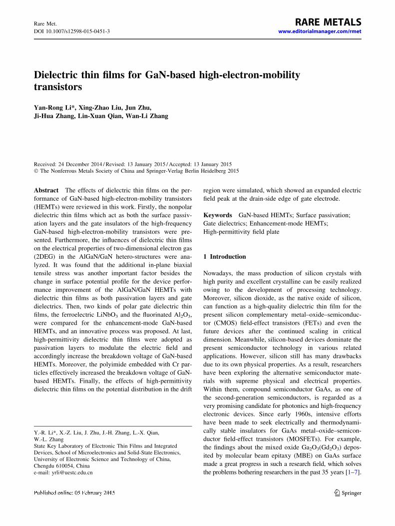
Chen [45] reported that the optimization of the potential
distribution in the drift region can be achieved by covering
a high-permittivity (HK) dielectric on the drain-gate region
of AlGaN/GaN HEMTs as shown in the inset in Fig. 9. The
electric field distribution in the AlGaN/GaN HEMTs with
and without a HK thin film covering the drain-gate region
was simulated by integrated system engineering technol-
ogy computer Aided design (ISE TCAD) as shown in
Fig. 9 [46]. The permittivity of HK thin film in this sim-
ulation is about 100. Because of the large difference in
permittivity between HK thin film and AlGaN barrier layer,
HK thin film can transmit an electric flux into or extract an
electric flux from AlGaN surface. As a result, the electric
field peak at the drain-side edge of gate electrode is wid-
ened by expanding to the entire gate-drain region, and thus
the breakdown voltage increases. In this method, HK thin
film acts as a field plate.
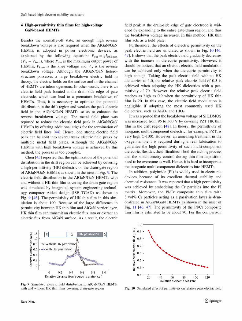
Furthermore, the effects of dielectric permittivity on the
peak electric field are simulated as shown in Fig. 10 [46,
47]. It shows that the peak electric field gradually decreases
with the increase in dielectric permittivity. However, it
should be noticed that an obvious electric field modulation
can be achieved only when the dielectric permittivity is
high enough. Taking the peak electric field without HK
dielectrics as 1.0, the relative peak electric field of 0.5 is
achieved when adopting the HK dielectrics with a per-
mittivity of 70. However, the relative peak electric field
reaches as high as 0.9 when the permittivity of HK thin
film is 20. In this case, the electric field modulation is
negligible if adopting the most commonly used HK
dielectrics, such as Al2O3 and HfO2.
It was reported that the breakdown voltage of Si LDMOS
was increased from 95 to 360 V by covering PZT HK thin
film in the drift region [48]. In theory, the permittivity of
inorganic multi-component dielectric, for example, PZT, is
very high ([100). However, an annealing treatment in the
oxygen ambient is required during a real fabrication to
guarantee the high permittivity of such multi-component
dielectric. Besides, the difficulties in both the etching process
and the stoichiometry control during thin-film deposition
need to be overcome as well. Hence, it is hard to incorporate
the inorganic multi-component dielectrics into HEMTs.
In addition, polyimide (PI) is widely used in electronic
devices because of its excellent thermal stability and
chemical resistance. It was reported that a high permittivity
was achieved by embedding the Cr particles into the PI
matrix. Moreover, the PI/Cr composite thin film with
8 vol% Cr particles acting as a passivation layer is dem-
onstrated in AlGaN/GaN HEMTs as shown in the inset of
Fig. 11 [46, 47]. The permittivity of the PI/Cr composite
thin film is estimated to be about 70. For the comparison
Fig. 9 Simulated electric field distribution in AlGaN/GaN HEMTs
with and without HK thin films covering drain-gate region Fig. 10 Simulated effect of permittivity on relative peak electric field
GaN-based high-electron-mobility transistors
123Rare Met.

purpose, both the AlGaN/GaN HEMTs only with PI pas-
sivation and without any passivation were investigated as
well. The transfer characteristics and trans-conductances of
AlGaN/GaN HEMTs are shown in Fig. 11 [46, 47]. It
shows that the passivation can benefit the DC performance,
and that the difference between PI and PI/Cr on the pas-
sivation effect is negligible. Furthermore, the measured
result related to the breakdown properties of AlGaN/GaN
HEMTs is shown in Fig. 12 [46, 47]. The breakdown
voltage is defined as the off-state source–drain voltage with
a source–drain current of 1 mA�mm-1. The breakdown
voltages of the AlGaN/GaN HEMTs without any, with PI
and with PI/Cr passivation are about 122, 156 and 248 V,
respectively.
In order to clarify the difference between PI and PI/Cr
passivations, the dependence of breakdown voltage on the
thickness of dielectric thin film was studied. As for the PI-
passivated AlGaN/GaN HEMTs, a weak relationship
between the breakdown voltage and the thickness of
passivation layer is observed as shown in Fig. 13 [46].
However, the breakdown voltage almost linearly increa-
ses with adding the passivation layer thickness in the PI/
Cr-passivated AlGaN/GaN HEMTs. Therefore, the
improvement in the breakdown voltage properties can be
attributed to the surface effect for the PI-passivated Al-
GaN/GaN HEMTs, while that for the PI/Cr-passivated
AlGaN/GaN HEMTs is ascribed not only to the surface
effect but also to the HK field plate, which is a bulk effect
and thus contributes the most to the breakdown voltage
enhancement.
5 Summaries
To sum up, several experimental innovations in device
process were achieved for GaN-based power HEMTs in
our past works. Firstly, the nonpolar dielectric thin films,
for example, Al2O3, were adopted as surface passivation
layer as well as gate insulator to improve the device per-
formance of AlGaN/GaN MISHFETs. Then, the enhance-
ment-mode GaN HEMTs were successfully fabricated
using polar gate dielectric thin films, such as the ferro-
electric LiNbO3 and the fluorinated Al2O3. In addition, the
polyimide embedded with nano-sized Cr particles as a HK
dielectric thin film with a passivation function was utilized
in GaN-based HEMTs so as to increase the breakdown
voltage.
Acknowledgments The work was financially supported by the
National Nature Science Foundation of China (No. 50932002) and the
Research Foundation for the Doctoral Program of Higher Education
of China (No. 2012018530003).Fig. 11 Transfer a and trans-conductance b characteristics of
AlGaN/GaN HEMTs (VDS = 10 V)
Fig. 12 Off-state current–voltage characteristics of AlGaN/GaN
HEMTs
Fig. 13 Effect of passivation layer thickness on breakdown voltage
of AlGaN/GaN HEMTs
Y.-R. Li et al.
123 Rare Met.

References
[1] Hong M, Mannaerts JP, Bower JE, Kwo J, Passlack M, Hwang WY,
Tu LW. Novel Ga2O3(Gd2O3) passivation techniques to produce
low Dit oxide-GaAs interfaces. J Cryst Growth. 1997;175–176:422.
[2] Ren F, Kuo JM, Hong M, Hobson WS, Lothian JR, Lin J, Tsai
HS, Mannaerts JP, Kwo J, Chu SNG, Chen YK, Cho AY.
Ga2O3(Gd2O3)/InGaAs enhancement-mode n-channel MOS-
FET’s. IEEE Electron Device Lett. 1998;19(8):309.
[3] Hong M, Kwo J, Kortan AR, Mannaerts JP, Sergent AM. Epi-
taxial cubic gadolinium oxide as a dielectric for gallium arsenide
passivation. Science. 1999;283(5409):1897.
[4] Kwo J, Hong M, Busch B, Muller DA, Chabal YJ, Kortan AR,
Mannaerts JP, Yang B, Ye P, Gossmann H, Sergent AM, Ng
KK, Bude J, Schulte WH, Garfunkel E, Gustafsson T. Advances
in high kappa gate dielectrics for Si and III–V semiconductors.
J Cryst Growth. 2003;251(1–4):645.
[5] Kwo J, Hong M. Research advances on III–V MOSFET elec-
tronics beyond Si CMOS. J Cryst Growth. 2009;311(7):1944.
[6] Shin B, Weber JR, Long RD, Hurley PK, Van de Walle CG,
McIntyre PC. Origin and passivation of fixed charge in atomic
layer deposited aluminum oxide gate insulators on chemically
treated InGaAs substrates. Appl Phys Lett. 2010;96(15):152908.
[7] Wang WK, Hwang JCM, Xuan Y, Ye PD. Analysis of electron
mobility in inversion-mode Al2O3/InxGa1-xAs MOSFETs. IEEE
Trans Electron Devices. 2011;58(7):1972.
[8] Bernat J, Gregusova D, Heidelberger G, Fox A, Marso M, Luth
H, Kordos P. SiO2/AlGaN/GaN MOSHFET with 0.7 lm gate-
length and fmax/fT of 40/24 GHz. Electron Lett. 2005;41(11):667.
[9] Liu C, Chor EF, Tan LS, Dong Y. Structural and electrical
characterizations of the pulsed-laser-deposition-grown Sc2O3/
GaN hetero-structure. Appl Phys Lett. 2006;88(22):222113.
[10] Chang YC, Lee YJ, Chiu YN, Lin TD, Wu SY, Chiu HC, Kwo J,
Wang YH, Hong M. MBE grown high kappa dielectrics
Ga2O3(Gd2O3) on GaN. In: Proceedings of the 14th Interna-
tional Conference on Molecular Beam Epitaxy (MBE XIV).
Tokyo, Japan. J Cryst Growth. 2007; 301:390.
[11] Chang YC, Chiu HC, Lee YJ, Huang ML, Lee KY, Hong M,
Chiu YN, Kwo J, Wang YH. Structural and electrical charac-
teristics of atomic layer deposited high k HfO2 on GaN. Appl
Phys Lett. 2007;90(23):232904.
[12] Maeda N, Hiroki M, Watanabe N, Oda Y, Yokoyama H, Yagi T,
Makimoto T, Enoki T, Kobayashi T. Systematic study of insu-
lator deposition effect (Si3N4, SiO2, AlN, and Al2O3) on elec-
trical properties in AlGaN/GaN hetero-structures. Jpn J Appl
Phys. 2007;46(2):547.
[13] Liu ZH, Ng GI, Arulkumaran S, Maung YKT, Teo KL, Foo SC,
Sahmuganathan V. Improved two-dimensional electron gas trans-
port characteristics in AlGaN/GaN metal-insulator-semiconductor
high electron mobility transistor with atomic layer-deposited Al2O3
as gate insulator. Appl Phys Lett. 2009;95(22):223501.
[14] Hu X, Koudymov A, Simin G, Yang J, Khan MA, Tarakji A,
Shur MS, Gaska R. Si3N4/AlGaN/GaN–metal–insulator–semi-
conductor hetero-structure field-effect transistors. Appl Phys
Lett. 2001;79(17):2832.
[15] Hsiao CY, Shih CF, Chien CH, Huang CL. Textured magnesium
titanate as gate oxide for GaN-based metal–oxide–semiconduc-
tor capacitor. J Am Ceram Soc. 2011;94(4):1005.
[16] Quah HJ, Cheong KY, Hassan Z, Lockman Z. Effect of post-
deposition annealing in oxygen ambient on gallium-nitride-
based MOS capacitors with cerium oxide gate. IEEE Trans
Electron Devices. 2011;58(1):122.
[17] Hashizume T, Kotani J, Hasegawa H. Leakage mechanism in
GaN and AlGaN Schottky interfaces. Appl Phys Lett.
2004;84(24):4884.
[18] Hashizume T, Ootomo S, Hasegawa H. Suppression of current
collapse in insulated gate AlGaN/GaN hetero-structure field-
effect transistors using ultrathin Al2O3 dielectric. Appl Phys
Lett. 2003;83(14):2952.
[19] Chini A, Wittich J, Heikaman S, Keller S, DenBaars SP, Mishra
UK. Power and linearity characteristics of GaN MISFETs on
sapphire substrate. IEEE Electron Device Lett. 2004;25(2):55.
[20] Kuzmik J, Pozzovivo G, Abermann S, Franc J, Carlin O,
Gonschorek M, Feltin E, Grandjean N, Bertagnolli E, Strasser G,
Pogany D. Technology and performance of InAlN/AlN/GaN
HEMTs with gate insulation and current collapse suppression
using ZrO2 or HfO2. IEEE Trans Electron Devices. 2008;
55(3):937.
[21] Simin G, Adivarahan V, Yang J, Koudymov A, Rai S, Asif Khan
M. Stable 20 W/mm AlGaN-GaN MOSHFET. Electron Lett.
2005;41(13):774.
[22] Chumbes E, Smart J, Prunty T, Shealy J. Microwave perfor-
mance of AlGaN/GaN metal insulator semiconductor field effect
transistors on sapphire substrates. IEEE Trans Electron Devices.
2010;48(3):416.
[23] Maeda N, Wang C, Enoki T, Makimoto T, Tawara T. High drain
current density and reduced gate leakage current in channel-
doped AlGaN/GaN hetero-structure field-effect transistors with
Al2O3/Si3N4 gate insulator. Appl Phys Lett. 2005;87(7):073504.
[24] Maeda N, Makimura T, Maruyama T, Wang C, Hiroki M, Yo-
koyama Y, Makimoto T, Kobayashi T, Enoki T. RF and DC
characteristics in Al2O3/Si3N4 insulated-gate AlGaN/GaN het-
ero-structure field-effect transistors with regrown ohmic struc-
ture. Phys Status Solidi A. 2006;203(7):1861.
[25] Maeda N, Makimura T, Maruyama T, Wang C, Hiroki M, Yo-
koyama H, Makimoto T, Kobayashi T, Enoki T. DC and RF
characteristics in Al2O3/Si3N4 insulated-gate AlGaN/GaN het-
ero-structure field-effect transistors. Jpn J Appl Phys. 2005;
44(21):L646.
[26] Wang C, Maeda N, Hiroki M, Tawara T, Saitoh T, Makimoto T,
Kobayashi T, Enoki T. Comparison of AlGaN/GaN insulated
gate hetero-structure field-effect transistors with ultrathin Al2O3/
Si3N4 bilayer and Si3N4 single layer. Jpn J Appl Phys.
2005;44(4B):2735.
[27] Wang CX, Maeda N, Hiroki M, Yokoyama H, Watanbe N,
Makimoto T, Enoki T, Kobayashi T. Mechanism of superior
suppression effect on gate current leakage in ultrathin Al2O3/
Si3N4 bilayer-based AlGaN/GaN insulated gate hetero-structure
field-effect transistors. Jpn J Appl Phys. 2006;45(1A):40.
[28] Koudymov A, Shur MS, Simin G, Chu K, Chao PC, Lee C,
Jimenez J, Balistreri A. Analytical HFET I–V model in presence of
current collapse. IEEE Trans Electron Devices. 2008;55(3):712.
[29] Vetury R, Zhang NQ, Keller S, Mishra UK. The impact of
surface states on the DC and RF characteristics of AlGaN/GaN
HFETs. IEEE Trans Electron Devices. 2001;48(3):560.
[30] Kim KW, Jung SD, Kim DS, Im KS, Kang HS, Lee JH, Bae Y,
Kwon DH, Cristoloveanu S. Charge trapping and interface
characteristics in normally-off Al2O3/GaN-MOSFETs. Micro-
electron Eng. 2011;88(7):1225.
[31] Tian BL, Chen C, Zhang J-H, Li Y-R, Chen YF, Liu X-Z, Zhou JJ,
Li L, Chen C. Structure and electrical characteristics of AlGaN/
GaN MISHFET with Al2O3 thin film as both surface passivation
and gate dielectric. Semicond Sci Technol. 2011;26(8):085023.
[32] Chang WH, Chang P, Lee WC, Lai TY, Kwo J, Hsu CH, Hong
JM, Hong M. Epitaxial stabilization of a monoclinic phase in
Y2O3 films on c-plane GaN. J Cryst Growth. 2011;323:107.
[33] Gila BP, Hlad M, Onstine AH, Frazier R, Thaler GT, Herrero A,
Lambers E, Abernathy CR, Pearton SJ. Improved oxide pas-
sivation of AlGaN/GaN high electron mobility transistors. Appl
Phys Lett. 2005;87(16):163503.
GaN-based high-electron-mobility transistors
123Rare Met.

[34] Koehler AD, Nepal N, Anderson TJ, Tadjer MJ, Hobart KD,
Eddy CR, Kub FJ. Atomic layer epitaxy AlN for enhanced Al-
GaN/GaN HEMT passivation. IEEE Electron Device Lett.
2013;34(9):1115.
[35] Hoffman J, Pan X, Reiner JW, Walker FJ, Han JP, Ahn CH, Ma
TP. Ferroelectric field effect transistors for memory applica-
tions. Adv Mater. 2010;22(26–27):2957.
[36] McCartney CL, Mitchell C, Hunta M, Ho FD. Design and
testing of a 1T-1C dynamic random access memory cell utilizing
a ferroelectric transistor. Integr Ferroelectr. 2014;157(1):1.
[37] Wu YR, Singh J. Polar heterostructure for multifunction devi-
ces: theoretical studies. IEEE Trans Electron Devices. 2005;52
(2):284.
[38] Chen C, Liu XZ, Tian BL, Shu P, Chen YF, Zhang WL, Jiang
HC, Li YR. Fabrication of enhancement-mode AlGaN/GaN
MISHEMTs by using fluorinated Al2O3 as gate dielectrics. IEEE
Electron Device Lett. 2011;32(10):1373.
[39] Chen C, Liu XZ, Zhang JH, Tian BL, Jiang HC, Zhang WL, Li
YR. Threshold voltage modulation mechanism of AlGaN/GaN
metal–insulator–semiconductor high-electron mobility transis-
tors with fluorinated Al2O3 as gate dielectrics. Appl Phys Lett.
2012;100(13):133507.
[40] Hao LZ, Zhu J, Liu YJ, Liao XW, Wang SL, Zhou JJ, Kong C,
Zeng HZ, Zhang Y, Zhang WL, Li YR. Normally-off charac-
teristics of LiNbO3/AlGaN/GaN ferroelectric field-effect tran-
sistor. Thin Solid Films. 2012;520(19):6313.
[41] Hao LZ, Li YR, Zhu J, Wu ZP, Deng J, Zeng HZ, Zhang JH, Liu
XZ, Zhang WL. Enhancing electrical properties of LiNbO3/Al-
GaN/GaN transistors by using ZnO buffers. J Appl Phys.
2013;114(2):027022.
[42] Zhang JH, Yang CR, Liu Y, Zhang M, Chen HW, Zhang WL, Li
YR. Can we enhance two-dimensional electron gas from ferro-
electric/GaN heterostructures. J Appl Phys. 2010;108(8):
084501.
[43] Liu XZ, Chen C, Zhu J, Zhang WL, Li YR. The modulation
effects of charged dielectric thin films on two-dimensional
electron gas in AlGaN/GaN heterostructure. J Appl Phys.
2013;114(2):027003.
[44] Xing HL, Dora Y, Chini A, Heikman S, Keller S, Mishra UK.
High breakdown voltage AlGaN–GaN HEMTs achieved by
multiple field plates. IEEE Electron Device Lett. 2004;25(4):
161.
[45] Chen XB. Lateral high-voltage semiconductor devices with
surface covered by thin film of dielectric material with high
permittivity. US Patent; 6936907.2005.
[46] Chu FT. Vapor deposition polymerized polyimide thin films for
miniaturized electronic devices. Chengdu: University of Elec-
tronic Science and Technology of China; 2014. 101.
[47] Chu FT, Chen C, Zhou W, Liu XZ. Improved breakdown
voltage in AlGaN/GaN high electron mobility transistorsby
employing polyimide/chromium composite thin films as surface
passivation and high-permittivity field plates. Chin Phys Lett.
2013;30(9):097303.
[48] Li JH, Li P, Huo WR, Zhang GJ, Zhai YH, Chen XB. Analysis
and fabrication of an LDMOS with high-permittivity dielectric.
IEEE Electron Device Lett. 2011;32(9):1266.
Professor Yan-Rong Li acade-
mician of the Chinese Academy
of Engineering, president of
University of Electronic Science
and Technology of China, was
born in 1962 in Sichuan Prov-
ince. In 1992, he got the Ph.D.
degree from Changchun Insti-
tute of Applied Chemistry,
Chinese Academy of Sciences.
He is currently the director of
the State Key Laboratory of
Electronic Thin Films and Inte-
grated Devices. He is engaged
in electronic thin films and
devices. He invented a novel bi-axial rotation method to fabricate
large-area double-sided YBCO superconducting thin films by inverted
cylindrical sputtering. Based on the study of the initial growth
mechanism, self-buffered architecture was proposed to improve the
reliability of pyroelectric thin film sensors for nondispersion infrared
detection. Now he is working at dielectric thin films for GaN HEMTs
and MMICs, thin film sensors for aircraft engine, and HTSC coated
conductors. He twice won the prize of National Technology Invention
Award. He has got more than 20 issued Chinese patents, published
more than 200 journal articles and three books.
Y.-R. Li et al.
123 Rare Met.


