DEVELOPMENT OF INDIUM-ANTIMONIDE TUO-DIMENSIONI. … · charge-injection device..cu) general...
34
RD-A127 716 DEVELOPMENT OF INDIUM-ANTIMONIDE TUO-DIMENSIONI. i/i CHARGE-INJECTION DEVICE..CU) GENERAL ELECTRIC CORPORATE RESEARCH AND DEVELOPMENT SCHENECTR. C WEI ET AL. UNCLASSIFIED APR 82 83SRDS25 N88i73-8e-C-e28i F/G 28/8, N
Transcript of DEVELOPMENT OF INDIUM-ANTIMONIDE TUO-DIMENSIONI. … · charge-injection device..cu) general...

RD-A127 716 DEVELOPMENT OF INDIUM-ANTIMONIDE TUO-DIMENSIONI. i/iCHARGE-INJECTION DEVICE..CU) GENERAL ELECTRIC CORPORATERESEARCH AND DEVELOPMENT SCHENECTR. C WEI ET AL.
UNCLASSIFIED APR 82 83SRDS25 N88i73-8e-C-e28i F/G 28/8, N

LI1
1111.25 Ila1_'. isi
t.6
11111 IIII,_____,
MICROCOPY RESOLUTION TEST CHARTNATIONAL BUREAU OF STANDARDS-1963-A
.. ... .. -.....-...... . ...... .
7. .
DEVELOPMENT OF INDIUM-ANTIMONIDETWO-DIMENSIONAL CHARGE-INJECTION DEVICE ARRAY
WITH COMPLETE CHARGE TRANSFER
Final Report
Contract No. N00173-80-C-0281
- Prepared for
Naval Research LaboratoryWashington. D.C. 20375
by
C.-Y. Wei and H.H. Woodbury
General Electric CompanyCorporate Research and Development
Schenectady, N.Y. 12301
April 1983 3
93SRD025

*. . . . . .
UNCLASSIFIED
S'LtURITy CLAs-II-CATION OF THIS PAGE (When Data Entereo)
READ INSTRUCTIONSREPORT DOCUMENTATION PAGE BEFORE COMPLETING FORM
" I RPURT NUMBER GOVT ACCESSION NO 3 RECIPIENT'S CATALOG NUMBER
S 4 TITLE (Snd S.,'i 5. TYPE OF REPORT & PERIOD COVEREDDevelopment of Indium-Antimonide Two-Dimensional Final ReportCharge-Injection Device Array with Complete Charge FinG ReportTrasfe 6 PERFORMING ORG. REPORT NUMBER
STransfe83SRD025
*I AUTHOR(34 B CON~TOR GRANT NUMBERUs)
C.-Y. Wei and H.H. Woodbury N01 7 3-8 0-C-02 81
9 PERFORMING ORGANIZATION NAME AND ADDRESS 10. PROGRAM ELEMENT, PROJECT. TASKGeneral Electric Company AREA L WORK UNIT NUMBERS
" Corporate Research and DevelopmentP.O. Box 8Schenectady, NY 12301
11 CONTROLLING OFFICE NAME AND ADDRESS 12. REPORT DATE
Naval Research Laboratory April 1982Washington, DC 20375 13. NUMBER OF PAGES
14 MONITORING AGENCY NAME & ADDRESS (of different fro,, Co.ntoit,, Office) 16. SECURITY CLASS, t (oi ,ep"
Unclassified15a. DECLASSFICATIONDOWNGRAOING
SCHEDULE
16 DISTRIBUTION STATEMENT (of this ReWIJ
Approved for public release; distribution unlimited.
17 DISTRIBUTION STATEMENT (ot the abstract *ntei d in Block 20. of different from Rawo
18 SUPPLEMENTARY NOTES
19 KEY WORDS (Continue on reirers. Side it necessar'y and Identify by block nlumberf)
infrared imaging array, charge injection device (CID),
indium-antimonide (InSb), MOS capacitor
20 AST T (Continue on reverse Side ,t neessary and ~nty by block numoer)A "non-etch-back" fabrication technique has been developed for an InSb two-
dimensional infrared sensitive charge injection device. This report sunuarizesthe first phase of a two phase program and describes the fabrication techniqueand test results on a set of experimental configurations.
The performance objectives relating to lag, well capacity, and charge trans-fer have been met. The second phase of this program has been initiated which isto fabricate the 16 x 64 2-D CID arrays.
".ORMDD ,JAN,1 1473 EDITION OF INOVSISOSOLETEL
SECUNCLASSIFIEDSECURITY CLASSIFICATION OF THIS PAGE (We Oslo EntW
TABLE OF CONTENTS
Section Page
- ABSTRACT .................................................. iv
1 INTRODUCTION .............................................. 1
2 GATE OXIDE FABRICATION .................................... 1
3 TEST ARRAY STRUCTURE AND FABRICATIONS ..................... 2
4 ARRARY TESTING SETUP ...................................... 2
5 RESUL.TS ................................................. 4
5.1 Characterization of Signal (Row) Gates in a FieldPlate Geometry ..................................... 4
5.2 Charge Transfer Characteristics ..................... 6
6 SUMMARY ................................................... 8
ACKNO EMENTS .......................................... 8
'4
LIST OF TABLES
Table Pago
.4 I S umary of Lag and Well Capacity Measurements ............. 9
Accession For
NTIS GRA&IDTIC TABUnannouncedJustificatio
Distribution/
Availability CodesAvail and/or
Dist Special
"" i
7777 . . . .. . .
LIST OF ILLUSTRATIONS
Figure Page
1 Etch-back (a) vrs non-etch-back (b) fabrication ............ 10
2 Nomarski micrographs of an as-deposited CVD SiO 2 film
about 1200 A thick (a) and of a film originallyabout 6000 A and then etched to about 1200 A (b) ........... 11
3 Distribution of breakdown voltages of NOS capacitorsfor three etching condition ................................ 12
4 Cross sectional schematics of the two test structuresfabricated ................................................ 13
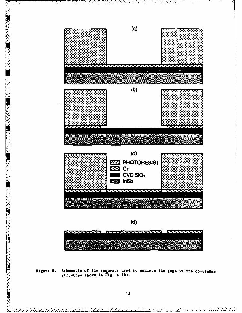
. Schematic of the sequence used to achieve the gaps in theco-planar structure shown in Fig. 4 (b) .................... 14
6 Optical micrograph illustrating the uniform gap widthachieved by the process illustrated in Fig. .............. 15
7 Two test patterns giving different transfer lengths betweenthe row and column gates or sensors ........................ 16
8 Bias and voltage injection connections for reading signaloff either substrate or gate pixel . ........... 17
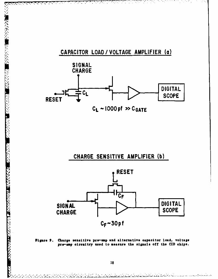
9 Charge sensitive pro-amp and alternative capacitor load.voltage pro-amp circuitry used to measure the signals offthe CID chips . ............................................ 18
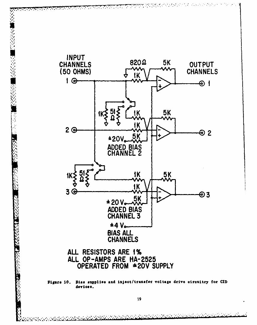
10 Bias supplies and inject/transfer voltage drive circuitryfor CID devices . .......................................... 19
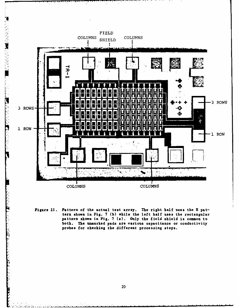
11 Pattern of the actual test array ........................... 20
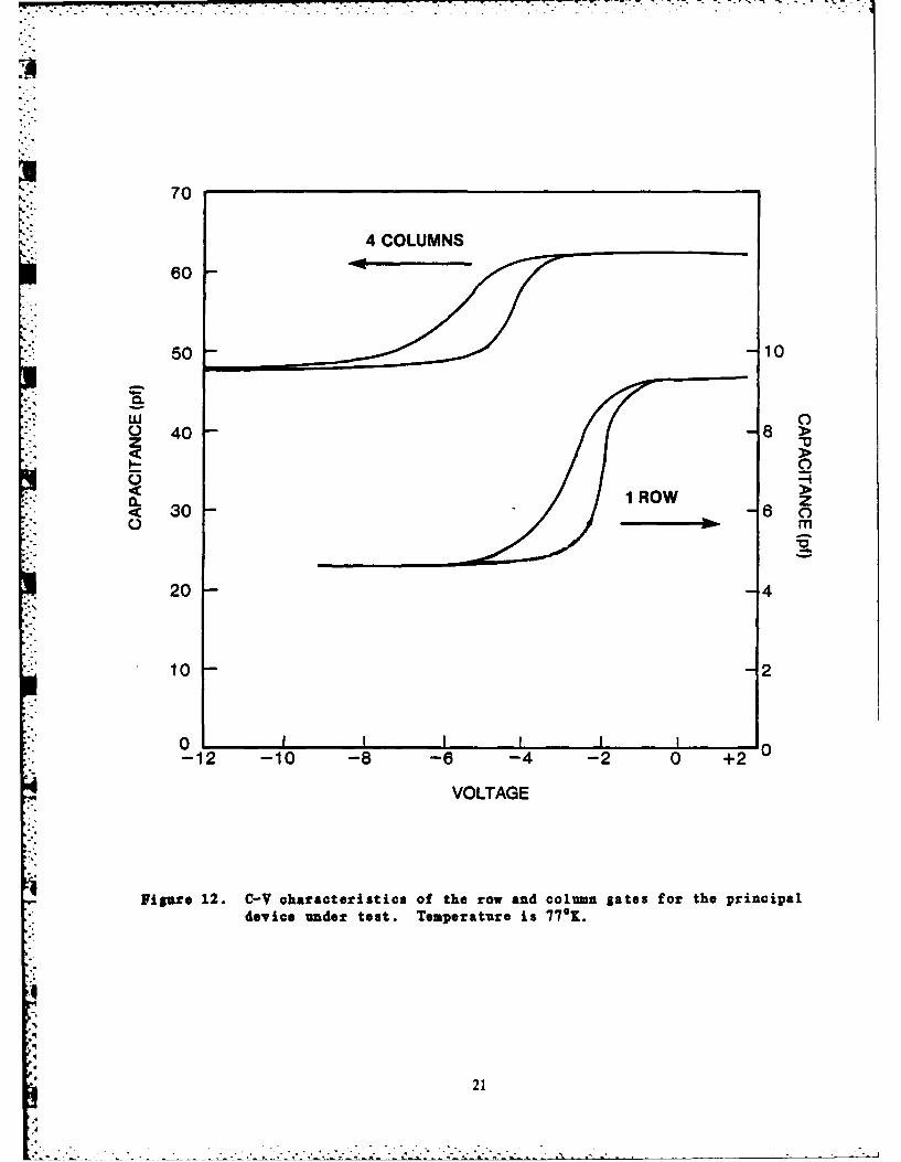
12 C-V characteristics of the row and column gates for theprincipal device under test ................................ 21
13 Typical results for a signal gate/field plate geometry(linear array configuration) ................................ 22
14 As Fig. 13 but column bias increased to -7.0 V ............ 23
15 Schematic of the potential wells and charge distributionsfor four possible 2-D readout schemes .................... 24
16 Demonstration of the Charge Sharing Mode .................. 25
17 Ideal Mode behavior under different dark current integrationtimes at 77K . ............................................. 26
W,
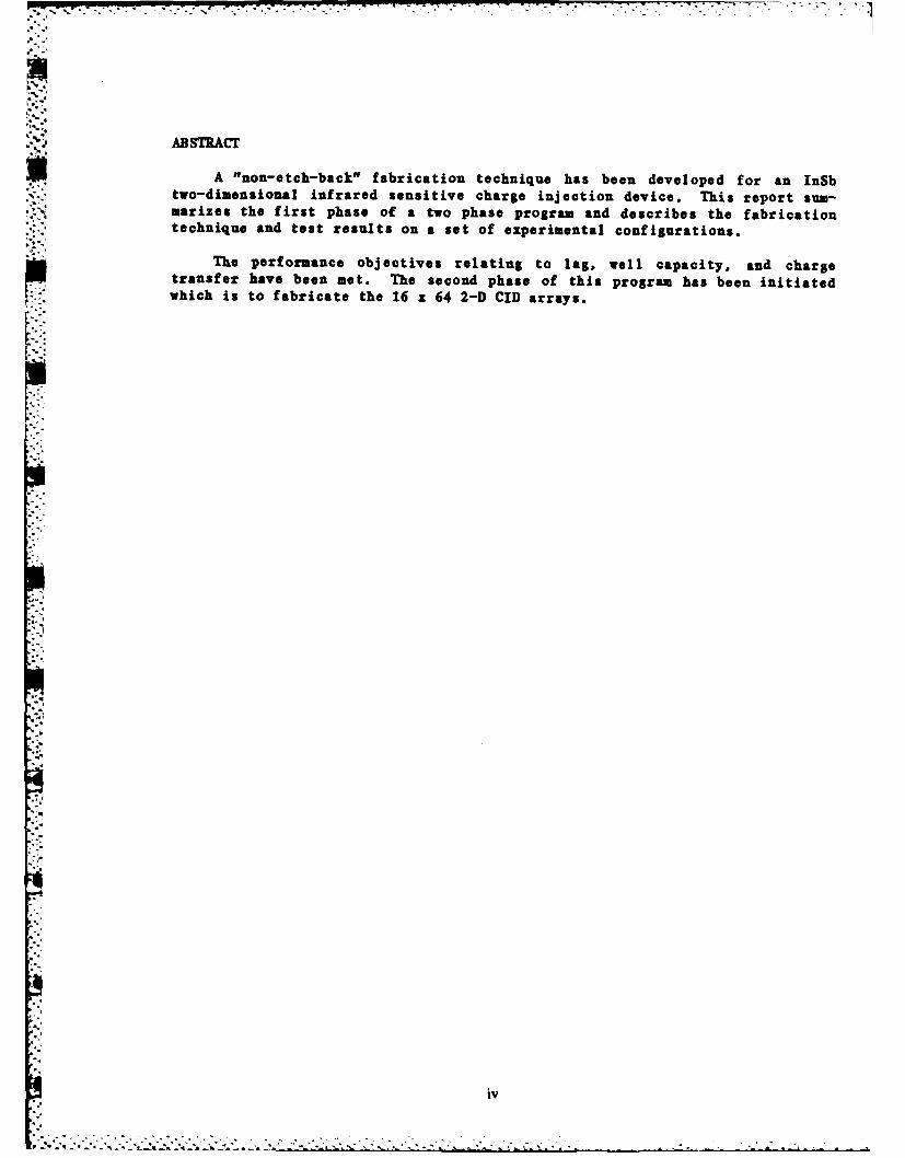
ABSTRACT
A "non-etch-back" fabrication technique has been developed for an InSbtwo-dimensional infrared sensitive charge injection device. This report sum-marizes the first phase of a two phase program and describes the fabrication
,, technique and test results on a set of experimental configurations.
The performance objectives relating to lag. well capacity, and chargetransfer have been met. The second phase of this program has been initiatedwhich is to fabricate the 16 x 64 2-D CID arrays.
iv
..................... ,
-. U - -- U . ., -- U*2" 2- - -
1. INTRODUCTION
The objective of this program is to demonstrate charge transfer in anInSb two-dimensional (2-D) charge injection device (CID) using a proposed"non-etch-back" array fabrication technique. In this technique the thicknessof the oxide layers employed in the CID fabrication are those "as-deposited"by chemical vapor deposition (CVD). Degradation of oxide quality and thick-ness uniformity due to oxide etching is avoided. CID arrays of improvedcharge transfer, low lag, reduced crosstalk, and improved uniformity inresponsivity and storage well capacity are expected. A high array yield canalso be realized because of the planar processing used in the "non-etch-back"technique.
This program was divided into two phases. Phase I was to design andfabricate test arrays and study the charge transfer characteristics. Thisphase also included the design of a Navy IRST 16x64 2-D CID array if the testarrays showed good charge transfer characteristics.
In Phase II the Navy IRST 16x64 2-D array will actually be fabricated andforty selected chips will be delivered to NRL for testing.
This final report describes the results obtained during Phase I of thisprogram. The gate oxide fabrication is first described in Section 2. Thedesign and fabrication of the test arrays are then given in Section 3. Thearray testing facilities are described in Section 4. Finally, the resultsobtained on the test arrays are presented in Section 5.
2. GATE OXIDE FABRICATION
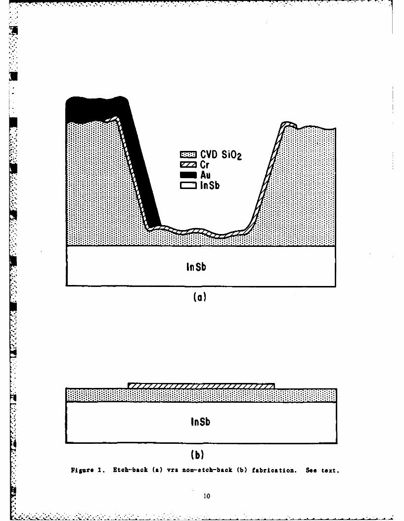
In contrast to the "etch-back" technique in which the gate oxide is
formed by selectively thinning from a thick oxide (see Figure la), the pro-posed "non-etch-back" technique consists of a 1500 A thick layer of as-
deposited CVD SiO2 for the Sate oxide and a layer of 75 A thick Cr film forthe sensing area metallurization (see Figure lb).
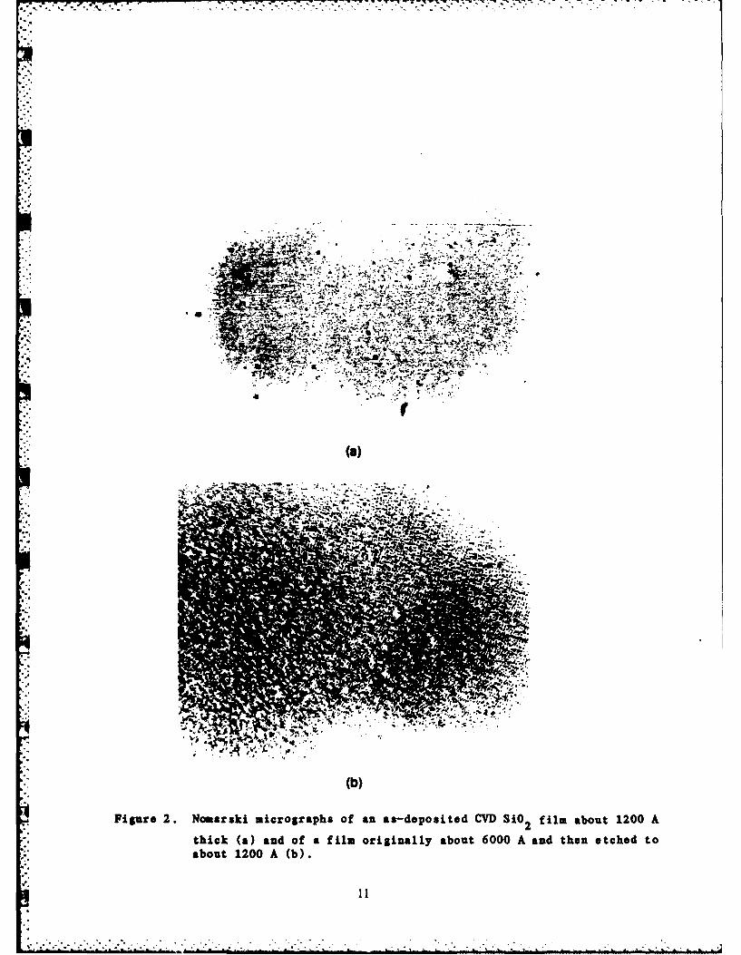
The deterioration of oxide films in the "etch-back" process is bestillustrated in Figures 2 and 3. Figure 2 shows two Nomarski micrographs ofsurface morphology for the as-deposited (see Figure 2a) and the etched oxidefilms of - 1200 A thick (see Figure 2b). The initial thickness of the etchedoxide film was - 6000 A. Note that the thin - 1200 A as-deposited oxide filmis featureless whereas the oxide after an extended etch in 3% BF appears to berough. The roughness of the etched surface can only be guessed but is of theorder of a few hundreds of Angstroms.
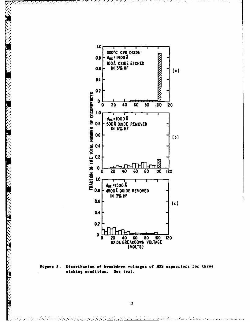
Figures 3a and 3b show the oxide breakdown voltages for oxide films whichhave been thinned by 100 and 500 A in 3% HF, respectively. The initial oxidethickness was 1500 A. It is clear that there is a significant degradation indielectric strength after chemical etch in 3% HF. The degradation of theseoxide films becomes worse if a layer of 4500 A thick oxide is removed from anoxide film of 6000 A initial thickness (see Figure 3c). Note that breakdownis observed down to OV and shows a broad peak at 20V. The oxide breakdownvoltage Is defined as the voltage necesjary to cause a 10 p A oxide leakagecurrent for SI-NOS capacitor of 1.14x10- on area.
I

3. TEST ARRAY STRUCTURE AND FABRICATIONS
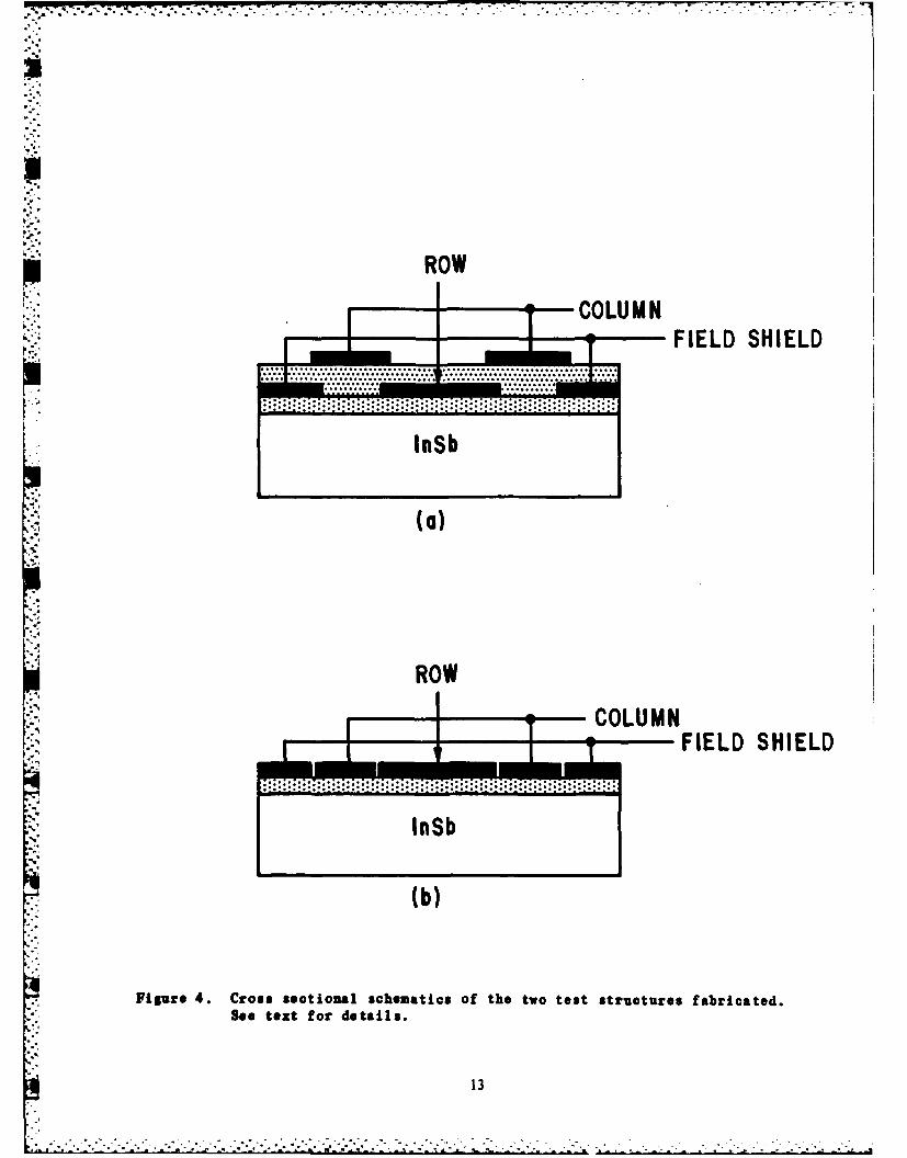
N Two test array structures were designed and fabricated during Phase I ofthis program. Figure 4 shows cross-sectional views of the two test struc-tures. In the first test structure the row sensor and the field shield arefirst patterned over a layer of - 1500 A thick oxide. A second layer of oxidefilm (- 1000A) is then deposited and the column sensor is finally defined.Note that the column sensor overlaps the row sensor to avoid any possiblecharge transfer barrier. The conducting films employed in Figure 4a are Cr of- 75 A thickness. The transmission of such films is - 70% at X = 4pm when ananti-reflective coat is used.
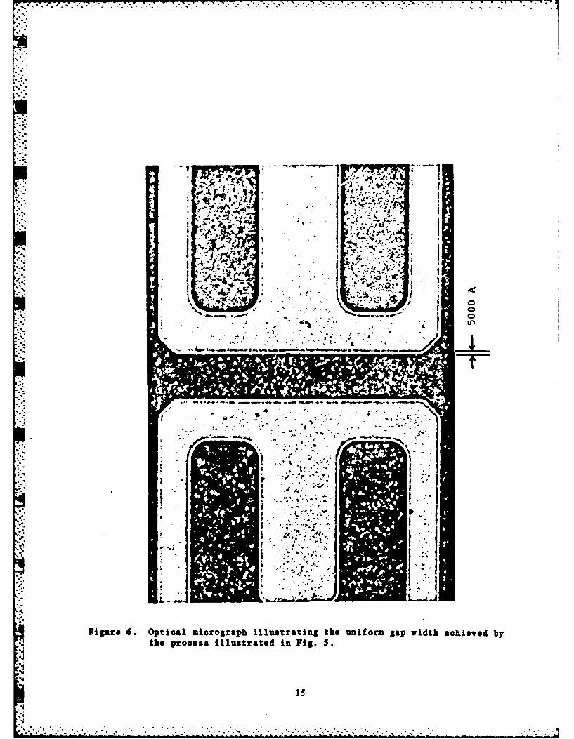
The cross-sectional view of the second 2-D test structure is shown inFigure 4b. In this test structure the row sensor, the column sensor, and thefield shield are separated by narrow gaps of ( 5000 A patterned over the sameoxide layer of - 1500 A thickness. The gap width between the row and columnsensors was achieved by a controlled undercut during the row gate patterningas illustrated in Figures 5a-5d employing a standard lift-off technique. Fig-ure 6 shows an optical micrograph of a test pattern exhibiting a gap width of
V- 5000 A, which has been chosen for convenience. Note that the edge defini-tion of the gap looks sharp and the gap width appears to be very uniform.
L'," The typical gap width employed in the array processing was - 3000A. Theadvantage of this second test structure over the first is that all the elec-trodes have the same oxide thickness which simplifies the array operation.
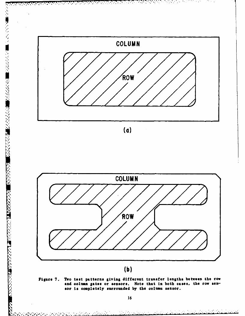
In addition to the two test structures described above, the test maskdesign included arrays of two different transfer lengths, i.e., the averagedistance the charge has to move to get from row to column or vice versa. Fig-
ure 7 shows the top-views of the two CID cells. Note that unlike the conven-tional side-by-side design, the row sensor is completely surrounded by thecolumn sensor, reducing the transfer length for a fixed area of sensing site.The transfer length in Figure 7 is - 20pim whereas in Figure 7b it is - 10pm.It should be noted that the cell geometries shown in Figure 7 are designed atthe expense of increasing the periphery-to-area ratio. The increased peri-phery will slightly increase the edge trapping and hence may reduce the chargetransfer efficiency. However, the benefit of the large increase in transferspeed will offset the small, if any, decrease in the transfer efficiency.
4. ARRAY TESTING SETUP
All the measurements described hereafter have been made on individualgates or on gates connected in parallel. Thus, any interaction or cross-talkbetween adjacent gates that might occur in an actual device with sequentialreadout schemes will not show up in these tests. The chips are given a prel-iminary screening for shorts and opens with conductance and C-V measurements.The latter also give an idea of the threshold voltages and any perculiaritiesin behavior which mostly arise from charges in the oxide or at interfaces.
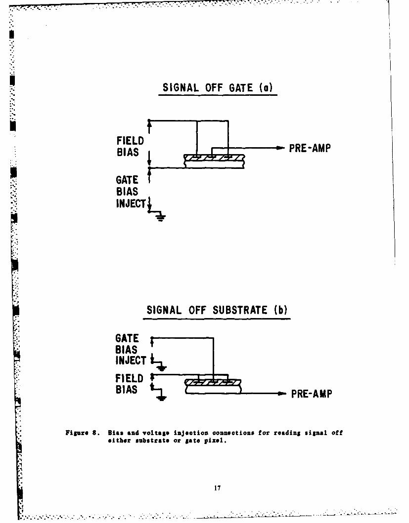
The principal parameters studied are well capacity, lag, and the transfercharacteristics between the row and column gates. The first two parametershave been measured with one of the set-ups shown in Figures 8 and 9. Figure 8shows, for a linear array, the injection and bias arrangements for reading theinjected charge either off the substrate or off the NO0 gate. Additional bias
2
supplies and injection pulses are required for 2-D arrays as noted below.Figure 9b schematically illustrates a charge sensitive pre-amp that was builton a small copper plate attached to the sample holder in the dewar vacuum.The 2N4416A input T-FET isolates the unacceptably high input bias current ofthe HA-2605 operational amplifier from the input. The 2N4416A is mounteddirectly on the copper plate and is thus cooled with the sample. This reducesits already low input bias current to a completely negligible amount. The HA-2605 is thermally isolated from the copper plate and is "heat" sunk to thewarm (outside) wall of the dewar through copper strip fingers since it willnot satisfactorily operate at low temperatures.
The absolute value of the charge signal is determined by the product ofthe output voltage and CT, the total feed back capacitance. The latter isdetermined by making a measurement (test pulses at room temperature are suffi-cient since the temperature dependence of the small mica capacitors that areused is small), and then adding a calibrated capacitor in parallel to CF andremeasuring the same signal. A comparison of the amplitudes of the two sig-nals will give C Alternatively, a small current, e.g., 1 p amp, is fedinto the input a&n the time rate change of the output voltage is determinedfrom the digital scope. It was found that the circuitry adds - 3 pf to CF.
Figure 9a shows a capacitor load, voltage sensitive pre-amp circuit. Theload capacitor, CL, must be much greater than the capacitance of the gate(s)measured, otherwise charge sharing occurs between the gate and load capaci-tances giving an "electronic lag'. The 2N4416A source follower serves thesame function as in the circuit shown in Figure 9b. Since there is no feed-back around this source follower, a constant current source supply is providedso that the gain is very close to unity.
The total load capacitance, Ci is calibrated the same as C in the cir-cuit shown in Figure 9b. BecausetT must be large (typically-7000 pf), thesignals are small and a pro-amp mustl-be used between the source follower andthe Nicolet digital scope. A 10 nsec rise time pre-amp with a nominal gain of50 was put together utilizing a SN72733 chip for this purpose. Because of thelarge value of CLT, wiring capacitances are of minimal effect and have noeffect on circuit stability. This permits all the electronics to be externalto the dewar. This in turn provides greater flexibility in testing a sample,once it is mounted and the dewar evacuated, since all pertinent sample leadsare directly brought out.
Both of the arrangements and circuits shown in Figures 8 and 9 have beenused. After concluding that these different arrangements did indeed giveidentical results, the combination shown in Figure 8a and 9a was adoptedbecause of the flexibility noted above and the fact that the dewar did nothave to be specially fitted with a pro-sap. Most measurements have been car-ried out with a dewar having two separate connectors with only the signal leadcoming out one connector. This minimizes electronic cross-talk.
In utilizing the arrangement as shown in Figure 8a, the injection pulsemust be applied simultaneously and equally to the field plate (or the columnsif they are used as field plates in testing the row gates) and the substrate.Since the read out circuit resets the signal gate(s) to ground potential, thesubstrate-signal gate potential must be applied to the substrate. However,
3
the behavior of the device is determined by any field plate and/or column gatepotentials with respect to the substrate. The circuitry shown in Figure 10provides this arrangement with considerable flexibility for testing linear or2-D arrays. Channel 1 is usually connected to the substrate. The dc inputpotential and any injection pulse supplied through input 1 can be added to anyadditional (positive and negative) biases and/or pulses in channel 2 or chan-nel 3. Channel 2, e. g., is usually connected to the column gates and channel3 to the field plate.
To measure the charge transfer behavior in 2-D devices, one more elec-tronic box was built. This is a counter and an electronic analog switchwhich, with the circuitry of Figure 10, permits the turning on or off of acolumn inject pulse after a pre-set number of row inject pulses, or viceversa.
The injection pulses and overall timing of the signals are generated byfour signal generators, specifically, Wavetek models 113 and 164 and/or Ail-tech model 511. This provides complete flexibility in the timing, amplitudes,and widths of the pulses required and is especially useful in carrying out thecharge transfer tests between row and column gates.
The handling of the chips was found to influence the threshold voltages,especially in structures with thin oxide layers and/or non-overlappinggate/field plate structures. This is presumably related to moisture and/orphoto effects charging the surface or inducing charges on interface states orbetween oxide layers. A vacuum annealing at 100*C for a few hours stabilizesthe thresholds as long as the detectors are kept in the dewar vacuum.
5. RESULTS
As noted above, the arrays have a concentric ring structure, i. e., eachcolumn gate completely surrounds a row gate. (The terminology of column androw is arbitrary. In this report, however, the above designation will alwaysbe used. namely, column gates will be those gates each of which surrounds arow gate.) This permits the column gates to act as a field plate to the rowgates since one has a local geometry similar to that of a linear array with afield plate. Figure 11 shows an example of a completed test array with allpertinent pads labeled.
A 2-D array with the second test structure (see Figure 4b) was wire-bonded and tested. This array shows normal C-V curves for both row and column
gates. Good charge transfer between row and column gates was also observedwhen the array was operated in the charge-sharing mode and the sequential rowinjection mode (see below). This array, however, showed some irreproducibil-ity in the bias conditions from day-to-day even when the array was kept invacuum. This was thought due to oxide charge-up over the unshielded gapbetween the row and column gates although very stable unshielded structureshave since been made. It was, therefore, concluded at that time to focus on
- the array development of the first test structure.
5.1 Characterization of Signal (Row) Gates in a Field Plate Geometry
44p 4
J.
. . . .C -. . .. .. . . . . . . . .
In the typical signal gate-field plate configuration, the field plate isbiased to threshold. This permits the maximum injection voltage to be appliedwhich is typically at least twice the maximum injection voltage in the casewhere the field plate is connected to the substrate.
Most Of the data has been taken on one device which has 1500 A oxideunder the signal (row) gates and 2000-2200 A oxide under the column gates.
The actual field plate developed partial shorts to the substrate and in allexperiments it was connected directly to the substrate. All the data reportedbelow was with an H pattern geometry, i.e., the signal (row) gate was Hshapedwith the column gate completely surrounding and overlapping it in geometri-cally complementary pattern (See Figure 7b).
Figure 12 gives the C-V characteristics of the row and column gates andthe approximate threshold voltages derived from these measurements. Thesethreshold voltages are typical following a two-hour anneal as described above.
Figure 13 shows typical data. The well (depleted volume) under the sig-nal gate is permitted to fill (invert) from dark current by waiting 0.5 to 5seconds. Usually, the cold infrared filter in the optical window is replacedby a copper plate so that the sample sees only the cold dewar temperature. In
Figure 13a, a series of readout sequences is shown starting at the left fol-lowed by the 2nd through 6th readouts following the dark current integrating
period. Looking at the 6th readout, the reset transient is first seen, thenthe injection pulse of 0.5 psec width (not resolved on the recording) followedby the actual signal and ending with the reset clamp. There is no significantdifference between the 6th signal and succeeding ones and this 6th signal istaken as the reference signal. The reference signal is sometimes referred to,in total, as the dark current signal but it is made up of at least threeparts: (1) The true dark current integrated between injection pulses of about
35 psec in this case. This dark current appears to be volume generated butwith a "volume-perimeterm component. (2) A reversible "breakdown" currentthat increases very non-linearly with injection voltage. This is the limitingfactor on the injection level and hence the well capacity. This breakdown is
dependent on the field plate bias involves the edge field enhancementeffects modeled by Tantraporn and Wei The injection voltage level appliedto the sample for the data shown in Figure 13a is just before the "breakdownpoint" as observed visually on the scope, i. e., there is less than a fewmilivolts contribution to the reference signal over the normal dark current.If the injection voltage is much too high, the signal clearly deviates fromthe straight line characteristic of a constant dark current (see Figure 13 b).Under such conditions, the breakdown current, presumably band-to-band tunnel-ing current, quickly flows into the deeply depleted well until the electric
fields are reduced below the breakdown levels. (3) Lag or the failure toinject all the charge in the previous injection pulse. Under typical condi-tions, this component is negligible for the 6th readout (since the well isnearly "empty") but is clearly seen in the 2nd readout following the largesignal in the 1st readout. Cross talk, or the recapture of injected charge by
1 W. Tantraporn and C.-Y. Wei, "Computer Simulation of the Electric Field inIndium-Antimonide Semiconductor under an MOS's Gate and Field Plate",General Electric Corporate Research and Development, Report No. 81CRD256,October 1 81.
5
an adjacent gate is minimal in these measurements because all the gates areread (injected) simultaneously.
Quantitatively, the signal on the 6th readout is taken as a reference or
the zero signal and the amplitudes of the preceeding signals are meas7Ted with
respect to it. Lag is defined as the ratio of the 2nd to the 1st signals andthe well capacity is calculated from the magnitude of the 1st signal. Theactual total charge collected in the well is closer to the sum of all the sig-nals since this tends to correct for any lag effects. However, the perfor-mance of a device is related to the magnitude of the 1st signal since thatwould be interpreted as the image signal.
As noted above, the data in Figure 13a is for the maximum injection vol-tage before non-linear "breakdown" effects are obvious with the column poten-tial set as negative as possible. The maximum injection voltage withoutbreakdown is quite dependent on the column (field plate) potential whereas theresults are insensitive to the row potential between -8 and down to at least-16 volts. The lag is seen to be 6.4% and the well capacity calculates out tobe
0.349 volts CL 7%G - 4.81x10 carriers
where CL = 1080 pf, G = 49 (preamp gain), and q is the electron charge. Themeasurements were carried out on a row of 8 gatel that were tied together onthe chip. Since each gate had an area of 6.76mils
well capacity 8.9x1 carriers mils-2.
With the dark current integration time reduced to 2 msec, the well isonly half filled. Under these conditions, the lag was measured to be 9.0%.Reducing the injection voltage to 0.82 volts (i.e., one-half) reduces the sig-nal to 137 mv and the lag was measured to be 9.3%. The increase in the lagnoted under these latter conditions is easily seen when running through aseries of measurements although the absolute accuracy of repeating lag meas-urements is no better than ± 1% from day to day.
If the column potential is made more negative, it was found that theinjection voltage, and hence well capacity, could be significantly increased.Figure 14 shows data on the same sample shown in Figure 13 illustrating theincreased well capacity without breakdown. The wells are permitted to fillwith a Ssec integration period and an equal and simultaneous injection voltageis applied to the column and row gates but only the row gates are read. Notethat with the thicker oxide under the column gates, the actual change in thesurface potential under the column gates is less than that under the rowgates. Table I summarizes these results.
5.2 Charge Transfer Characteristics
6
Many readout schemes for 2-D arrays require transferring the signal
charge and all or part of any background charge from row to column gates orvice versa. The efficiency and speed of transfer are important points in con-sidering certain schemes. Several of these schemes have been considered andbasic tests have been carrried out on the transfer modes involved. The rela-tive merits of these various schemes in potential 2-D systems are not con-
sidered here since the object is to demonstrate the dynamic responses of the
basic modes in a simple 2-element (one row, one column) hook-up. Figure 15illustrates a comparison of the potential wells during the elemental readcycle for four common readout schemes, i. e., the normal charge sharing mode(CSM), the sequential row injection mode, the ideal mode readout, and thequasi ideal mode. Note that for the sequential row inject, all rows are readsimultaneously (there is no row select) which requires a pre-amp for each row.It is also noted that for the first two modes it is only important that therebe a significant common background charge under a row/column pair. Figure 15illustrates only this common charge and does not imply the necessity or evenusual occurrence of an equal surface potential.
a) Normal Charge Sharing Mode
In the normal charge sharing mode (CSM), both the column and row gates
are in deep inversion and tightly coupled together. The biases on the row andcolumn gates are not critical since it is not necessary to empty either well.The charge is shared between the row and column and the output corresponds to1/2 the injected charge or signal.
This mode is demonstrated in Figure 16. In the two sequences shown,"injection/transfer" pulses are applied only to the row gates for the first 6
readouts whereas beginning with the 7th, injection pulses are applied to boththe row and column gates. In the lower sequence, a long (0.5 sec) integrationtime occurs before the 1st readout and the wells are completely filled. Thus,charge is injected in the first readout (pulse on the row gates only). Fol-
lowing this injection, the signal wells are half filled, as illustrated inFig. 15, and immediate repeated injection on the row gates only transferscharge to the column gates and is not injected.
Figure 16a is a case where the wells are only partially filled by limit-
ing the integration time to 0.5 msec. Here, no charge is injected in thefirst readout, but charge is transferred to the partially empty column andthen returned, hence, no signal is seen. The presence of the transferredcharge is indicated on the 7th readout where, as in Figure 16b, an injectionpulse is applied to both the row and column gates, charge injection takesplace, and a signal is seen. The integration time was set to give the maximum
* signal without injecting on the first readout, hence the signal applitude onthe 7th readout is similar for the two tracings. An important point is that
the signal is "sharp", i.e., in this tightly coupled, highly inverted case,the charge moves quickly as well as efficiently.
b) Sequential Row Inject Modes
The sequential row inject mode differs from the charge sharing mode inthat the wells are permitted to fill completely with signal and only the firstinject (i.e., select row or select column) voltage pulse is applied. This
7
mode is illustrated in the first read out in Figure 16b. With only the oneinjection, however, the injection voltage can be doubled without emptying the
* -, well to breakdown. This has been observed.
c) Ideal Mode
Ideal modes are where a limited bias voltage is applied to both the rowand column gates and all the well charge is transferred between them. This issimilar to a normal CCD operation and while this makes the simplest configura-tion conceptually, the bias and injection voltages are critical. Figure 17illustrates the device behavior in an approximate ideal mode which is usefulfor observing charge transfer behavior. The slow response indicates a "slow-moving" charge in getting the column well emptied into the row well followingthe row injection pulse. The charge, however, is not lost as evidenced by anunchanged signal following 1 or 10 such initial pulse readouts. Following theinjection pulses on both row and column gates (5th readout in this case), theopposite is seen, namely, a slow decay of minority carriers under the rowgates. It is believed that charge transfer indeed occurs in the ideal modebut the charge appears to move slowly and less efficiently. In addition, therequirement of critical biasing conditions for both row and column will likelymake this mode of operation impractical.
d) Quasi Ideal Mode
When the row bias is increased beyond the injection voltage, bias chargewill always be present under the row gate sensors (see Figure 15d). Signalcharge is then integrated under the row sensor until it starts to spill overunder the column sensor. The signal charge is first read out from the row andagain transferred to column. In the quasi-ideal mode no charge is sharedbetween row and column during readout or reference and hence all the signalcharge is read out. However, charge is shared between row and column duringrow select which gives high charge transfer efficiency. These features plusthe fact that the row bias is no longer critical, makes this a very attractivemode ot operation.
. 6. Summary
In summary, the feasibility of fabricating InSb CID 2-D array withimproved cnarge transfer characteristics has been successfully demonstrated ontest arrays fabricated by the proposed "non-etch-back" technique. Good chargetransfer has been obtained for devices operated in the normal charge sharingmode, the sequential row injection mode, and the quasi-ideal mode, Chargetransfer was also observed in the ideal mode but the charge appeared to moveslowly and less efficiently. These encouraging results on these test arrayshave given us confidence in designing a Navy IRST 16x64 2-D array for time-delay-and-integration application. This array is presently being fabricatedand tested.
Acknowledgements
- L.J. Keifer, H.M. Lees, and R.S. Lewandowski assisted in the fabricationand testing of these devices. H.K. Burke aided in mask designs.
o.8
7;-'.,.7777- 7 %
TABLE I3Summary of Lag and Well Capacity Measurements. Gate Bias = -12.0 V.Field Bias (Column Gates) = -5.3 V. In the Last Entry the Column
Gate Bias = -7.0 V.
INJECTION•IIECTION PULSE WELLVOLTAGE WIDTH LAG CAPACITy.(106/mil"
VOLTS ( sec) () (10
1.67 0.50 6.4 0.89
y 1.67 0.50 9.3 (half filled)
0.82 0.50 8.4 0.35
1.67 1.0 3.9 0.93
3.56 0.50 7.5 2.17
i
*9
r ~.:CYD SiO2* ~ Cr
AuC-1InSb
InSb
(a)
InSb
Fi~ure 1. Etch-back (a) vrs non-etch-back (b) fabrication. S.. text.
10
*:t~4'* .. rj . j.
rWit I.'
FigureS 2.Not' ico rh of ana-eoie V i imaot10
L~fl4' 2
thik () nd f afim oigialy aout600 Aandthn eche tabout 1200 A&%(b).
1.0 *
200C CVO OXIDE
0.8 do,: 1400-'001 OXIDE ETCHED
0.6 IN 3%HF ()
c 0 20 40 60 80 100 120
1.0 , , I
do,," 1000 A0.8 50A OXIDE REMOVED
cc IN 3% HF(hi
.a 0.2
0
20 40 60 80 100 120-., o-- 1.0, , , , ,
d : 150010.8 45001 OXIDE REMOVED
IN 3% HF0.6 -
0.4 -
0.2
0 o 20 40 60 80 100 120OXIDE BREAKDOWN VOLTAGE
(VOLTS)
Figure 3. Distribution of breakdown voltages of MOS capacitors for three
etching condition. See text.
12
ROW
I~ T FIELD SHIELD......... .. ... ........ .
InSb
(a)
ROW
COLUMN
FIELD SHIELD
......... .................. ****..
InSb
: : (b)
Figure 4. Cross sectional schematics of the two test structures fabricated.
See text for details.
13
(a)
(b)
Ow- -- - CV S-0-
.tutr . how.in.i....(b)
14
7 .
4 4
7'6.
Figure 6. Optical micrograph illustrating the unif orm gap width achieved bythe process illustrated in Fig. S.
,I COLUMN
*. ROW
(a)
-,' COLUMN
'
__4
i (b)
Figure 7. Two test patterns giving different transfer lengths between the rowand oolumn gates or sensors. Note that in both oases, the row sen-sor is completely surrounded by the column sensor.
16I
,4 .- ' -. . ' " '- - - ' ' *"". , " *.- ,,r,. t.*--.. . . . . ... " -.- " ,, p. .m ' ' l ' m ' ( ' ' - ' ' - L " a ' ' - L "
n,,L,.
. SIGNAL OFF GATE (a)
* F-FIELDFIELD [~711 - PRE-AMP
BIAS_
IGATEBIAS
rv" INJECTL,
SIGNAL OFF SUBSTRATE (b)
BIAS
INEC
FIELDBIASPRE-AMP
Figure 8. Bias and voltage injection connections for reading signal offeither substrate or gate pixel.
17
-INJECT ...
0,%
CAPACITOR LOAD/ VOLTAGE AMPLIFIER (a)
SIGNALCHARGE
RESET
CL IO00pf >CGATE
CHARGE SENSITIVE AMPLIFIER (b)
RESETL
CF tCOF
!!SIGNA IIA
,;,t'-; CF '- 300p
Figure 9. Char$* sessitive pre-amp and alternative capacitor load, voltagepo-smp circuitry used to measure the signals off the CID chips.
-18
;° " " ..""""" " "' " """. '""-" ." * ' " "" """ "" " '"".. ..................... -.I8 ..
INPUTCHANNELS 820 5K OUTPUT(50 OHMS) CHANNELS
4'K
51, IK 5K: " ' IK
& 20V 5K2
~ADDED BIAS~CHANNEL 2
ADDED BIASCHANNEL 3
BIAS ALLCHANNELS
ALL RESISTORS ARE I%ALL OP-AMPS ARE HA-2525
.* OPERATED FROM *20V SUPPLY
Figure 10. Dias supplies and injeot/traasfe voltage drive circuitry for CIDdevices.
19
FIELDCOLUMNS COLUMNS
• SHIELD
-4t
1 • 1 + 3 ROWR
_ Figure 11. Pattern of the actual teat array. The right half uses the H pat-~torn shown in Fig. 7 (b) while the left half uses the rectangularpattern shown in Fig. 7 (a). Only the field shield is common to. both. The unmarked pads are various capacitance or conductivityprobes for checking the different processing steps.
20
70
4 COLUMNS
60
50 -10
Q.w 0)o 40 -8 >
< 30 6___0
20 -
10 -
01 1 -8 -6 -4 -2 0 +
VOLTAGE
Figure 12. c-v characteristics of the row and column gates for the principaldevice under test. Temperature is 77*K.
12
I
(a) V 1 .67 V
(b) Vr2.6V
Figure 13. Typical results for a signal gate/field plate geometry (lineararray configuration). From data such as this, the lag and wellcapacity can be calculated. The row bias is -12.0 V. The colu~mnbias (acting as a field shield) is -5.3 V. The injection width is0.5 ILsec. The sample is at 77K and the row well is permitted tofill for 5 sec with dark current before the first injection pulseillustrated. Typical maximum injection voltage, V1, is shown in
* (a) while Wb illustrates signal when overdriven.
22
I ,?

V, i3.56 V
Figure 14. As Fig. 13 but column bias increased to -7.0 V. Note lack ofbreakdown with high injection voltage. Compare with Fig. 13b.
23
() CHARGE SNARING (b) SEQUENTIAL (c) IDEAL MODE (d) QUASI IDEALM' ." ODE ROW INJECTION MODE
NODE
CR R N 0 C
j INTRATION. 1 I l 5NERTN INTEGRATIONNTGANTEIRATION
READ NOW READ ROWS ED ROW
SELECT NOW-SELECT RON READ COLUMN SELECT ROW
INJECT INJECT INJECT INJECTCOLUMN COLU M N COLUMN COLUMN
REFERENCE EFERENCE REFERENCE REFERENCEROW ROWS COLUMN ROW
Figure 15. Schematic of the potential wells and charge distributions for fourpossible 2-D readout schemes. See text for a description of each.Thedashes represent the maximum possible injected charge andhence the maximum signal charge or well capacities. The slantlines represent excess inversion charge. R and C represent rowand column gates, respectively. For simplicity, the coluan gatesand wells are drawn adjacent to the rows whereas in the deviceunder test, each row Sate has a concentric column structure sur-round it. The READ and REFERENCE functions, of course, are inter-changeable since it is the injected charge or the difference inthe Sate charge before and after injection that is measured.Threshold voltage is represented by the "tops" of the wells.
24
* .- C - . I .
E(a T,--' 0. m m m
IT
(b) T1-O.5msec
ROW INJECT ROW AND COLUMNi'. ONLY INJECT
~~Figure 16. Demonstration of the Charge Sharing Mode. The samnple is at 77K[.
Raw bias - -12.0 V; row inject - 0.65 V. Column bias - -15.0 V,
Pc;. column inject - 0.85 V width of injection pulses is 1.0 psec. Seetext for a description of the pulse sequences.
25
:!:2
f- (a) T- 1.25 msc
123 m M(b) T- 2.5 msec
67 my
(c) T- 0.5 sec
1t t t t t t t t tROW INJECT ROW AND COLUMN INJECT
ONLY
Figure 17. Ideal Mode behavior under different dark current integration timesat 77K. Row bias - 6.73 V: row inject - 0.54 V. Column bias -
-9.24 V; column inject - 1.77 V. Width of injection pulses is5.4 psec. The first four sequences are with a row inject voltageonly. For the fifth sequence and on, the inject voltages areapplied simultaneously to both row and column gates. For T -
I1.25 msec, the row well is 1/2 filled (as measured to the bottomof the column well). For TI - 0.5 sec, both wells are filled and
the excess charge (for ideal mode operation) is injected in thefirst (row) injection pulse.
26
fop V,~a-ll-
I -. .44
Wkrn
U. 4
.t4*
II
41
'4 3-& A
r 04,