Develop a Cellular Radio System for Wireless Speaker
27
Transcript of Develop a Cellular Radio System for Wireless Speaker


The goal of this project is to design and develop a cellular radio system for a
wireless speaker based on cellular radio telephone concept and microcontroller for
application at offices, homes, lecturer hall, and hostel and etc. This project is acted as
a "Portable Announcing System (P.A)", the user can make an announcement to his
or her staff, friends, family via h s or her mobile phone even user is talking far away
from destination, or stranded in traffic jam. So that, the staff, friends, or family
members of the user can hear the announcement as long as there is a radio coverage
by a particular cellular phone system for two mobile phones. This project has a lot of
benefit and suitable for someone who have limited time or someone who always
busy to spent time to make important announcement which can be made in P.A
room. All the detail about this project being pulls in together in this thesis with all
the information which needed in separate chapter.

ABSTRAK
Tujuan utama projek ini ialah mernbangunkan satu sistem radio bimbit untuk
pembesar suara tanpa wayar menerusi konsep pengawalan mikro untuk diaplikasikan
di pejabat, umah, bilik kuliah dan hostel. Projek ini bertindak sebagai "sistem
pembuat pengumuman secara serba boleh" di mana para pengguna boleh membuat
pengumuman kepada para pekerja, kawan ataupun keluarga walaupun pengguna
berada di mana-mana tetapi mesti di dalam lingkungan liputan yang dikhaskan
syarikat komunikasi yang terdapat di negara ini. Projek ini sesuai kepada sesiapa
sahaja yang selalu sibuk dalam melakukan tugas tetapi perlu sentiasa membuat
pengumuman dan dengan adanya projek ini masa dan tenaga boleh dijimatkan.
Semua maklumat-maklumat penting bagi projek ini telah disiapkan dan setempatkan
dalam bab-bab yang telah disediakan di dalam tesis ini.

CHAPTER 1
INTRODUCTION
This chapter wills explain about project introduction, objectives, problem
statement and project scope.
1.1 INTRODUCTION
What is cellular? Cellular or mobile phone is one of the fastest growing and
most demanding telecommunications applications. Today, it represents a
continuously in~reasing~percentage of all new telephone subscriptions around the
world. Currently there are more than 45 million cellular were that regular subscribers
worldwide. It is forecasted that cellular systems using a digtal technology will
become the universal method of telecommunications. Other than that, technology
today is moving towards the future of the wireless web. Mobiles devices such as
palmtops, handheld and cellular phones are becoming all the rage. People want these
devices to do everything fiom access their e-mail accounts, to utilize the Internet, to
access personal and corporate information.

The goal of this project is to design and developing a cellular radio system for
a wireless speaker based on cellular radio telephone concept and microcontroller for
application at offices, homes, lecturer hall, and hostel and etc. This project is acted as
a "Portable Announcing System (P.A)", the user can make an announcement to his or
her staff, friends, family via his or her mobile phone even user is talking far away
from destination, or stranded in traffic jam. So that, the staff, fnends, or family
members of the user can hear the announcement as long as inside the radio coverage
by a particular cellular phone system for two mobile phones. Figure 1.1 shows basic
for this project combination between hardware and software for developing cellular
radio system for wireless speaker.
Figure 1.1 : Basic Block Diagram for Project
Main Board
PIC 16F84A
L
4
Sound Activate Switch
A
Mobile Phone
- 'I
Power Amplifier Speaker

1.1.1 Mobile Phone
A mobile phone or cellular phone is an electronic telecommunications device.
Most current mobile phones connect to a cellular network of base stations (cell sites),
which is in turn interconnected to the public switched telephone network (PSTN)(the
exception are satellite phones). In addition to the standard voice function of a
telephone, a mobile phone can support many additional services such as SMS for text
messaging, packet switching for access to the Internet, and MMS for sending and
receiving photos and video, [I].
Some of the world's largest mobile phone manufacturers include Alcatel,
Siemens, LG, Motorola, Nokia, Panasonic (Matsushita Electric), Philips, Samsung,
Sanyo, Sharp, Sony Ericsson, and Toshiba. The entire largest mobile phone
manufacturer always design a new type mobile phone and upgrade function to make
their product popular and their system also fiiendly user, guide user using mobile
phone correctly.
There are also specialist communication systems related to, but distinct from - - - -
mobile phones, such as Professional Mobile Radio. Mobile phones are also distinct
from cordless telephones, which generally operate only within a limited range of a
specific base station. Technically, the term mobile phone includes such devices as
satellite phones and prepcellular mobile phones such as those operating via MTS,
which do not have a cellular network, whereas the related term cellular phone does
not. In practice, the two terms are used nearly interchangeably, with the preferred
term varying by location, [I] .

1.1.2 Relay
Relay contacts on most of the industrial world are labeled with NO (Normally
Open), NC (Normally Closed), and C (Common). These labels and the function of
the relays seems to cause a great deal of confusion among people, however once the
operation of these relay being understand of the meaning it is quite simple and literal,
The first thing need to know is that a relay contact is a switch, nothing more,
nothing less. It does not provide power; it simply opens and closes an electrical
circuit, just like the light switch on a wall. When the relay is de-energized or turned
off there is an electrical connection between NC and Common, hence it was
normally closed. In the off state there is not a connection between NO and common,
hence normally open. When the relay is being energized it's turned on the NO and C
makes an electrical connection, and the electrical connection between NC and C
being removed, [2].
The last issue is voltage and current ratings. A typical relay rating will be
24VDC @ 5 Amps, llOVAC @ 10 Amps, 220 VAC @ 5 Amps. This is simply
telling the max amperage ba t the relay contacts can handle at the voltage the user
used. For example a 100 Watt light bulb is going to be about 100 VAC @ 1 Amp.
This is 9 Amps below the rating, so the circuit can handle turning on an off the light
bulb with no problem.

1.1.3 Power Amplifier
This is a 50 Watt stereo amplifier module design using the TDA 2009 from
Philips. It is particularly suited to battery operation, providing 50 Watt per channel
from only a 6VDC supply and it will operate best from 6-12 VDC and requires no
heat-sink for normal use. The TDA 2009A is class AB dual Hi-Fi audio power
amplifier assembled in Multiwatt package, specially designed for high quality stereo
application as Hi-Fi and music centers. The benefits of this power amplifier are short
circuit protected, thermal protection, low power consumption, good stability and gain
is internally set to 39 dB.
1.1.4 PIC 16F84A
The PIC16F84A belongs to the mid-range family of the PICmicroO
microcontroller devices. The program memory contains 1 K words, which translates
to 1024 instructions, since each 14-bit program memory word is the same width as
each device instruction. The data memory (RAM) contains 68 bytes. Data EEPROM
is 64 bytes. There are also 13 I/0 pins that are user-configured on a pin-to-pin basis. - - --
Some pins are multiplexed with other device functions. These functions including
external interrupt change'on PORTB interrupts and timer clock input, [3].
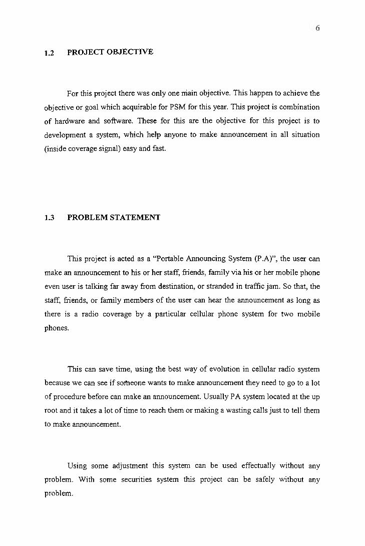
1.2 PROJECT OBJECTIVE
For this project there was only one niain objective. This happen to achieve the
objective or goal which acquirable for PSM for this year. This project is combination
of hardware and software. These for this are the objective for this project is to
development a system, which help anyone to make announcement in all situation
(inside coverage signal) easy and fast.
1.3 PROBLEM STATEMENT
This project is acted as a "Portable Announcing System (P.A)", the user can
make an announcement to his or her staff, &ends, family via his or her mobile phone
even user is talking far away fiom destination, or stranded in traffic jam. So that, the
staff, fiends, or family members of the user can hear the announcement as long as
there is a radio coverage by a particular cellular phone system for two mobile
phones.
This can save time, using the best way of evolution in cellular radio system
because we can see if someone wants to make announcement they need to go to a lot
of procedure before can make an announcement. Usually PA system located at the up
root and it takes a lot of time to reach them or making a wasting calls just to tell them
to make announcement.
Using some adjustment this system can be used effectually without any
problem. With some securities system this project can be safely without any
problem.

1.4 PROJECT SCOPE
For the project scope all the importaht thing had being made including all the
important measurement to make this project successfully without any flaw and
problem.
Some research had being made to make some requirement to create a
prototype for this project. For this project 50 Watt audio power amplifier had being
chosen because of small input (12 VDC) which suitable for the mobile phone. All the
signal and design being monitor all the time to make this amplifier work properly.
Make some research about PIC 16F84A microcontroller and learning some of
it benefits and the way it operated. Some program being added to this PIC 16F84A to
make it can be suitable for this project. Some adjustment being make to make PIC
16F84A circuit can match with power amplifier.
For mobile phone the Nolua had being chosen because the design of Nokia is - - - -
friendly user and this' mobile phone also cheap than other branded. The speaker, 8
ohm and 150 Watt being choose it suitable for this project and it can match with
power amplifier. The size of speaker can be choosing depending to the Watt of
power amplifier being crated.
The operation of this project, signallinput entering handset (part of project) or
handset receiving incoming call. The signal/input also entering PIC 16F8A which
had been programming to automatic "on" the incoming call or to hang-up the handset
without manually answer. PIC 16F84A will let the signal entering power amplifier.
The power amplifier will increase the volume of signal to make sure the input can be
heard anyone is the calculate range.


2.1.1 Description IC TDA 2009
The IC TDA2009A is class AB dual Hi-Fi audio power amplifier assembled
in Multiwaq package, specially designed for high quality stereo application as Hi-Fi
and music centers. The Figure 2.1 and Figure 2.2 show the picture and pin
connection for TDA 2009.
The input for thls IC TDA 2009 is shown in Table 2.1 and the maximum the
IC TDA 2009 can handle the heat of incoming energy (power supply) also can be
seen in Table 2.2. Table 2.3 show the electrical characteristic which can be accept by
the IC TDA 2009 otherwise the IC will blow because over voltage or for refemng to
the stereo application circuit, Tamb = 25 OC, VS = 24 V, GV = 36 dB, unless
otherwise specified.
MU LTlW ATTl1
ORDERING NUMBER : TDA2009A
Figure 2.1 : IC TDA 2009

N.C. wmn (11 +vs OUTPur ( 2 ) N.C. GNO ND)s 1NU INPUT (2) INN INPUT (2 ) Sv RH INX INPUT (1) NON I N K l W T ( 1 )
Figure 2.2: Pin Connection
Table 2.1 : Absolute Maximum Rating
P Table 2.2: Thermal Data
I Symbol I Parameter Value I unit I
Symbol
\IS
I,
lo
P, T,. Tj
I R I Theml Resistance Junction-case Max. 1 3 c:cf~
Parameter
Suppty Voltage Output Peak Current (repetitwe f 2 20 Hz)
Output Peak Current (non repetitive, t = 100 11s) Power Dissipation at T, = 90 T Storage and Junaon Temperature
Value 28
3.5 4.5
20
-40, + 150
unit v A
A W
<C


2.1.1.3 Mounting Instruction
The power dissipated in the circuit'must be removed by adding an external
heat sink. Thanks to the MULTWAT'T package attaching the heat sink is very
simple, a screw or a compression spring (clip) is being sufficient. Between the heat
sink and the package it is better to insert layer of silicon grease, to optimize the
thermal contact, no electrical isolation is needed between the two for IC TDA 2009.
The AN-6551 is a dual operational amplifier with a phase compensation
circuit built-in. It is suitable for application to various electronic circuits such as
active filters and audio pre-amplifiers. This IC AN-6551 had being used in this
power amplifier prototype and Figure 2.3 and Table 2.4 shown data about IC AN-
6551.
The AN-6551 features phase compensation circuit, high gain, low noise, . - --
output short-circuit protection and two circuits symmetrically arranged in 9-pin SIL - -
plastic package. Figure 2.4 show display block diagram for AN-6551 and Table 2.5
and Table 2.6 shown the data of the IC AN-655 1 including maximum rating in the IC
can handle and the electrical characteristics for VCC = 15V, VEE = -1 5 V, Ta = 25
"C.


:a c,
3 g B
. - . z
-0
g L,
% - ' '9'1 I
2
ti
~n
0
.E
ll
11
+I
I
z
All
/XI
.!"'I1 FZI
62 &
'
I,
U
3
wo
o
zs
w
11
+I
I m
o
.- 2
~~
~~
+I
1
g! =L
I
>a
;/
F2 I -1
+I
-3-
WP
,O
'"
-.
g- 4 +I
I A .L=-
I -
->
%%
@>
>>
@2
3
11
8
f
+I
+I 1
I


The outputs of both one-shots are connected to the input pins of a NOR gate.
When both inputs of AND gate U2A are at a logic 0, the output will be at a logic 1.
This output pulse is then coupled to the input of the flip-flop.
2.2.6 The Flip-Flop
A flip-flop, or a bistable multivibrator, is a circuit whose output logic level
changes when a pulse is applied to the input. The output will remain at its logic state
until the next pulse is applied. The only two possible output states for a flip-flop are
logic 1 and logic 0, [I, 4,5].
The IC 4558 is a quad 2 neither input CMOS NOR gate. The first NOR gate
is used as its primary purpose, a NOR gate. The next two NOR gates are configured
as a flip-flop.
When pin 4 is at logic 1, or 9 volts, pin 10 will be at logic 0. The voltage
divider o f ' ~ 1 5 and R14 sets pin 6 at approximately 2 volts. The voltage needed at the - - input of the NOR gates to switch the outputs from one state to the other is between
4.5 and 5.5 volts. It can'be seen that the voltage at pin 6, when pin 4 is at logic 1, is
biased at less than the trigger voltage. Capacitor C9 couples the output pulse from the
first NOR gate to the input of pin 6.
The pulse is now "riding" on the DC level at pin 6. The peak of the pulse is
now high enough in amplitude to reach the trigger level of the flip-flop. The flip-flop
will now trigger causing its output logic state to change. When pin 4 is at logic 0, pin
10 will be at logic 1. The trigger pulse is then coupled into pin 8 through capacitor
C8 to change the output state of the flip-flop. The last NOR gate is used as an
inverting buffer to separate the input of the transistor switch from the output of the
flip-flop, [ I , 4, 5, 61.