Detecting ZnS Thin Films on Si Substrates Using X-ray ...
18
Detecting ZnS Thin Films on Si Substrates Using X-ray Diffraction Thesis by: Benjamin Howorth In partial fulfillment of the requirements for the degree of: BS in Optical Physics Adviser: Dr. Janet Tate Oregon State University Physics Department Corvallis, Oregon. Submitted April 17 th, 2013 1
Transcript of Detecting ZnS Thin Films on Si Substrates Using X-ray ...

Detecting ZnS Thin Films on Si Substrates Using X-ray Diffraction
Thesis by:
Benjamin Howorth
In partial fulfillment of the requirements for the degree of:BS in Optical Physics
Adviser:
Dr. Janet Tate
Oregon State University Physics DepartmentCorvallis, Oregon.
Submitted April 17th, 2013
1

Table of Contents
Abstract/Acknowledgments -------------------------------------------------------------------------------------- (4)
Chapter 1. Introduction ---------------------------------------------------------------------------------------- (5)
Previous Work --------------------------------------------------------------------------------------------- (5)
Diffraction ------------------------------------------------------------------------------------------------- (5)
Three dimensional lattice -------------------------------------------------------------------------------- (7)
Crystal Types ---------------------------------------------------------------------------------------------- (8)
X-ray Source ---------------------------------------------------------------------------------------------- (9)
Spectrometer --------------------------------------------------------------------------------------------- (10)
Sample production -------------------------------------------------------------------------------------- (11)
Chapter 2. Measurement Methods -------------------------------------------------------------------------- (11)
Sample description -------------------------------------------------------------------------------------- (11)
Setup of XRD System ---------------------------------------------------------------------------------- (12)
Alignment ------------------------------------------------------------------------------------------------ (13)
Filters and Beam Focus -------------------------------------------------------------------------------- (13)
Measurement Settings ---------------------------------------------------------------------------------- (14)
Analysis -------------------------------------------------------------------------------------------------- (14)
Chapter 3. Results, Discussion, and Analysis ------------------------------------------------------------- (15)
Chapter 4. Conclusions ---------------------------------------------------------------------------------------- (17)
References -------------------------------------------------------------------------------------------------------- (18)
2

List of Figures
1.1 Constructive interference ------------------------------------------------------------------------------------ (6)
1.2 Lattice Vectors ------------------------------------------------------------------------------------------------ (7)
1.3 Lattice Planes -------------------------------------------------------------------------------------------------- (7)
1.4 Sphalerite and Wurtzite Models ----------------------------------------------------------------------------- (8)
1.5 Energy Transitions -------------------------------------------------------------------------------------------- (9)
1.6 Measurement Diagram -------------------------------------------------------------------------------------- (10)
1.7 Example Spectra --------------------------------------------------------------------------------------------- (10)
2.1 Sample Picture ----------------------------------------------------------------------------------------------- (12)
3.1 TEM Image --------------------------------------------------------------------------------------------------- (15)
3.2 ZnS on Si Spectrum ----------------------------------------------------------------------------------------- (16)
List of Tables
2.1 Peak Positions ------------------------------------------------------------------------------------------------ (12)
3
Abstract
The goal of this research is to determine whether x-ray diffraction (XRD) is a viable method for resolving ZnS thin films on Si substrates. The samples are ZnS thin films of thickness between 50nm and 100nm, on Si substrates that are 0.5mm thick.
ZnS and Si have nearly identical lattice parameters and can be interfaced well. They have different absorption spectra, allowing for more efficient solar cells. Research into applications is being done by graduate student Christopher Reidy, as well as methods of ZnS deposition on Si substrates.Nearly identical lattice constants is a good quality for solar cells, which can increase the efficiency considerably. Tunneling electron microscopy (TEM) is a method that directly images the interface, and provides a large amount of information about the interface and quality of a sample. However, it is both costly and time consuming compared to XRD. Research into the process of XRD will determine whether ZnS thin films can be resolved on the Si substrate to produce the same information in a matter of hours rather than days.
The scope of this paper includes an introduction to Bragg's law, crystal lattice structure, process descriptions, and conclusions drawn from the results. Ultimately, ZnS Intensity peaks were not observed in the XRD measurements on the Si intensity background.
Acknowledgments
I would like to express my gratitude to Dr. Janet Tate and graduate student Christopher Reidy for being my advisers and guides in researching the process of XRD. They were supportive, and more often than not, patient through the course of this project. This thesis would have not come into existence without their insight and effort. They gave me the much needed supportive pushes, and encouragement to keep the ball rolling. I could have ask for better role models. To both of them I give my heartfelt thanks.
I would also like to thank the other students and associates of the Tate lab group for their continuous input. Weekly group meetings kept the various projects on task, adding motivation and a sense of community to the lab.
Finally, I would like to thank the Oregon State University physics department for being my home over the past two years. Thanks to the Society of Physics Students, which provided both food and a place to sleep on late nights. Thanks to all my friends and family who accepted my frustrations and rejoicing alike through these years. I wish my fellows well on their own research and adventures in life.
4

Introduction
X-ray diffraction (XRD) is an experimental tool that is commonly used to examine crystal structure and thin films. The basic concept originates from Bragg's law; by diffracting light through a lattice it is possible to determine properties of a given sample, mainly the composition and the quality of crystal structure. The x-ray beam incident on the sample produces constructive interference at certain angles, depending on the lattice parameters and quality of the crystal. For this research it will be applied to thin films of zinc sulfide on a silicon substrate.
The process of XRD is a tool used for many applications. In this research, it is used to examine the structure of zinc sulfide thin films on silicon substrates. The samples are part of a much broader project, with the goal of producing a highly efficient solar cell. Silicon is effective for absorbing wavelengths below blue/UV light, but nothing above that. Zinc sulfide will absorb everything above UV, so combining the two will produce a solar cell that convert the majority of incident light into electricity (using hetero-junction assisted impact ionization). While there are many materials that absorb short wavelengths of light, zinc sulfide was chosen because it has a lattice constant almost identical to silicon. This allows for a very smooth interface between the two materials. Ideally, tunneling electron microscopy (TEM) would be used to examine every sample, since it provides clearer and more accurate results. However, it costly and far more time consuming than XRD. So the goal here is to optimize the use of x-ray diffraction in quickly examining thin film samples. More specifically, to find out if x-ray diffraction will produce the resolution required to gain the desired information about a sample. This information includes: whether the sample is single crystal or polycrystalline, and whether the zinc sulfide peaks can be observed against the much larger silicon background.
Previous Work
X-ray Diffraction is a well understood technique which has been used to examine many properties in material science. However, no work has been published regarding the process itself and it's ability to resolve small intensity peaks. This is because projects using XRD are subjective to the material(s) being examined, as well as the particular XRD system being implemented. A secondary goal of this work is to provide a foundation for determining the usefulness of XRD for a project.
Diffraction
Bragg's law, equation 1, is the driving concept behind x-ray diffraction; where n is an integer from 1 to ∞, λ is the wavelength of light, d is the slit spacing, and in this case θ is the incident angle. In this usage of Bragg's law, the slit spacing is the lattice spacing (called the lattice constant) of the crystal.
(1)
5

A crystal's structure is comprised of periodic atom blocks (unit cells) connected together. These unit cells form the crystal's lattice, which the x-rays will diffract through. Theoretically these unit cells are perfectly identical, with no other materials present. Unfortunately, this is not entirely the case. Atoms of other elements can attach themselves to the crystal lattice during the deposition process, creating perturbations and strain. The lattice can be broken into many groups with different orientations, making the sample polycrystalline. Part of the reason for examining the x-ray diffraction process is to have a fast and easy way of determining whether the sample is single crystal (one large lattice) or polycrystalline. If the sample is polycrystalline then the data will have peaks in strange places, indicating multiple orientations. If the lattice is simply doped with oxygen, which is common during deposition, then the existing peaks will broaden.
The diffraction occurs as incident x-rays are scattered by planes of atoms, as shown by the two dimensional example in figure 1.1. Bragg's law comes from the condition for constructive interference, an integer number of wavelengths must equal the total path difference.
Figure 1.1The two photons constructively interfere at certain angles as they are absorbed and re-emitted
by the atoms in the lattice.Image by Christophe Dang Ngoc Chan
A diffracted beam is one composed of a large number of scattered rays reinforcing each other. The only angles that will produce constructive interference are those satisfying Bragg's law, where the total path difference, 2dsin(θ), is an integer number of wavelengths. In these few directions the resultant (diffracted) beam is strong compared to the sum all scattered rays, but very weak compared to the incident beam. This is because the atoms only scatter a small portion of the incident energy. Notice that the constructive condition depends on the spacing d. In three dimensions this is the lattice constant of the material, the length of one unit cell. A three dimensional lattice introduces more planes of atoms through which scattering and constructive interference can occur.
6

Three Dimensional Lattice
For scattering from a three dimensional lattice, it is necessary to index each plane of atoms. This is done with a system called miller indices. Any point in a lattice can be described by an integer number of vectors as shown in figure 1.2.
.Figure 1.2
The locations of each atom in a cubic unit cell can be described by the vectors a, b, and c.Image by Ben Howorth
It is possible to describe a point anywhere in space by using non-integer values of the vectors a, b, and c. However, they can be converted to a set of smallest integers by multiplication or division, which is the common convention. The orientation of planes in a lattice can be represented with these indices, which provide a good frame of reference. A plane is described by the intercepts it makes with the crystallographic axes. The intercepts are written as the reciprocals of the fractional intercepts which the plane makes with the crystallographic axes. Essentially the plane is tilted by three integer numbers of lattice vectors, (hkl), as shown in figure 1.3.
Figure 1.3Different planes of atoms in cubic unit cells, listed by their miller indices.
Image by Christophe Dang Ngoc Chan.
7

In this way, the diffracted beams can be designated as originating from a plane (hkl). The planes are commonly pictured in a single unit cell, however they repeat periodically with the entire lattice. This index system is the reference for diffraction in three dimensions, but it is necessary to alter Bragg's law such that it includes the plane tilting information. The actual form depends on the shape of the unit cell of the crystal. In the research done here, the lattice is made up of cubic unit cells. The spacing between planes, d', now depends on their orientation, and can be written in the form:
(2)Where a is the lattice constant of the material being examined. Applying this new spacing to
Bragg's law gives a generic equation relating the incident angle to the plane of diffraction.
(3)Using this relation, the data can be analyzed in terms of indices (hkl), which correspond to
diffraction angles. Here, the angle at which constructive interference occurs depends on the lattice constants for zinc sulfide and silicon.
Crystal Types
The zinc sulfide lattice can be arranged in two ways to form different crystals, wurtzite and sphalerite. Figure 1.4 shows the difference between these two forms of ZnS. Wurtzite is a hexagonal formation that does build on cubic unit cells. Sphalerite has a cubic lattice which will ideally create a smooth interface between the ZnS and Si, so it is the desired structure for these thin films.
Figure 1.4The left image is a hexagonal wurtzite, while the right is a cubic sphalerite lattice.
Image by Ben Howorth
8
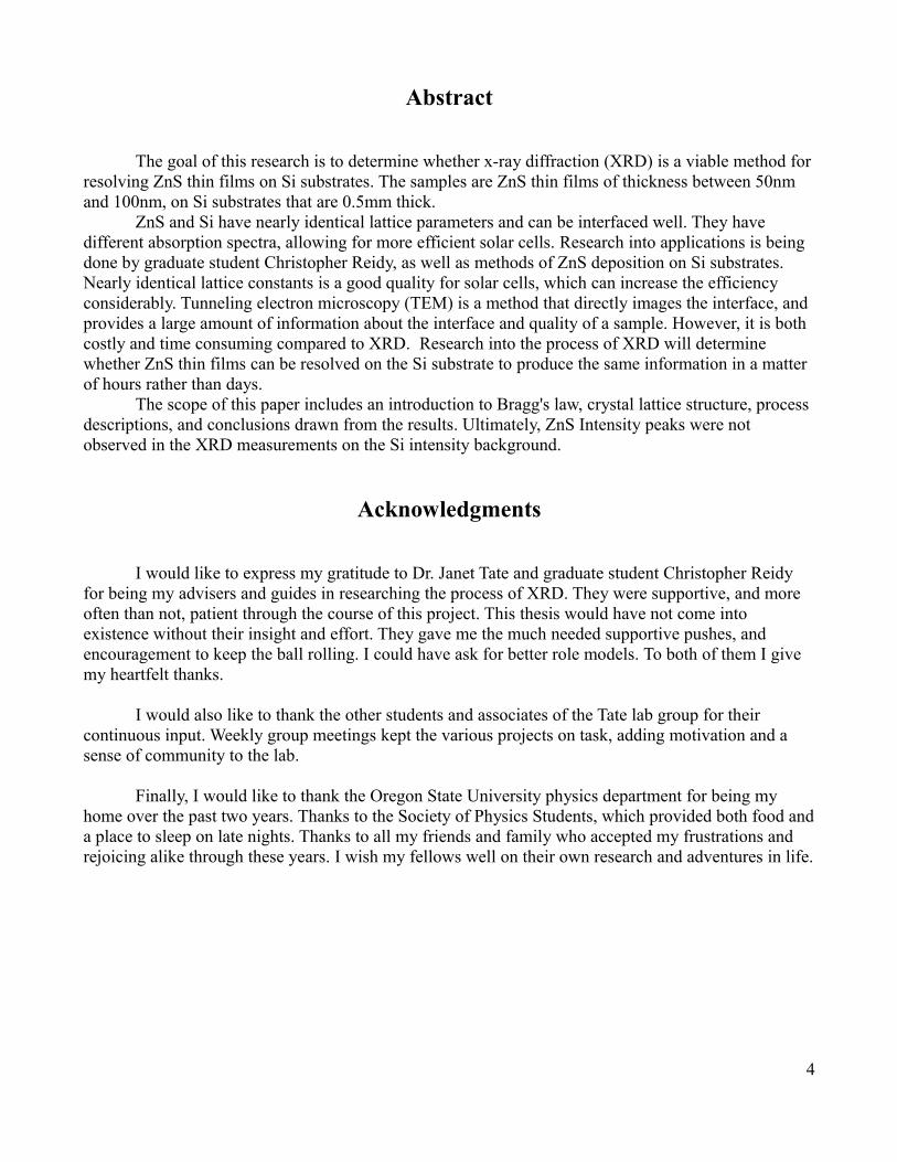
X-ray Source
The x-rays are produced by electrons impacting a metal target, which is copper in the system used here. They eject electrons from shells in the target atoms, leaving a hole. When another electron drops to fill the newly created hole, it generates a photon with a wavelength dependent on the target material energy states. There are three main transitions that we are concerned with: The Kα1
wavelength, which occurs with a transition from the 2P3/2 to 1S orbital, the Kα2 wavelength, which occurs with a transition from the 2P1/2 to the 1S orbital, and the Kβ emission which occurs with a transition from the 3P to the 1S orbital. Figure 1.5 shows the energy transitions for copper.
Figure 1.5Energy transitions in copper which result in x-ray wavelength photon emission
Image by Pieter Kuiper.
There are a few other wavelengths that are represented in the data, such as tungsten emissions, which are accounted for in the analysis. These wavelengths are the most prominent ones that the x-ray source produces, and provide the greatest intensity measurements. Because of this, they will be used to potentially identify the ZnS thin film on the Si substrate.
9
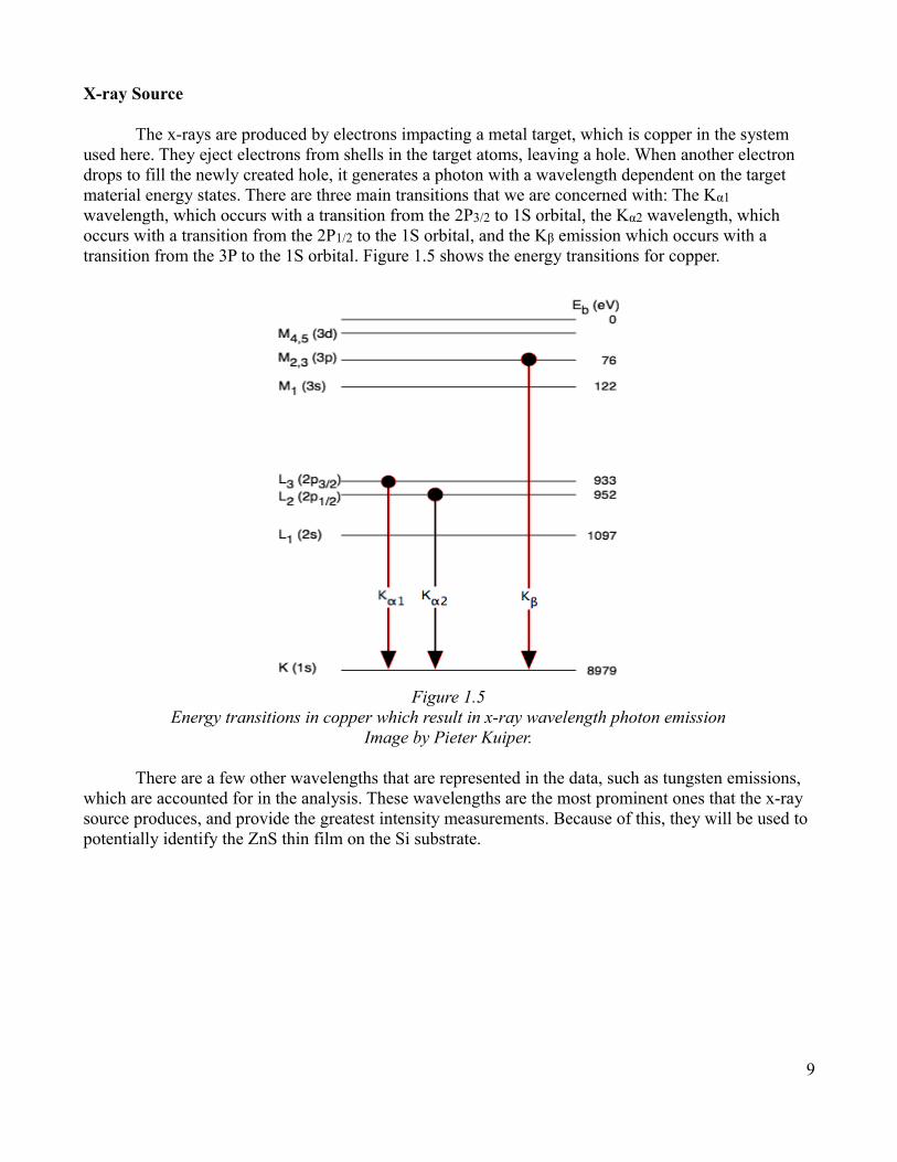
Spectrometer
The basic layout of the source, sample stage, and detector are shown in Figure 1.6.
Figure 1.6The x-ray source and detector move together along the dotted path, with the sample on the sample
stage.Image by UC Davis Chemwiki
To take a measurement the source moves up along the angle θ, as the detector follows. The
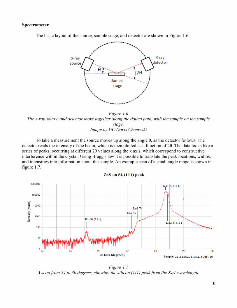
detector reads the intensity of the beam, which is then plotted as a function of 2θ. The data looks like a series of peaks, occurring at different 2θ values along the x axis, which correspond to constructive interference within the crystal. Using Bragg's law it is possible to translate the peak locations, widths, and intensities into information about the sample. An example scan of a small angle range is shown in figure 1.7.
Figure 1.7A scan from 24 to 30 degrees, showing the silicon (111) peak from the Ka1 wavelength.
10

Sample Production
The samples are made using pulsed laser deposition, where a laser evaporates a target (zinc sulfide) which then coats the silicon wafer inside the same vacuum chamber. The depositing of the ZnS is a delicate procedure; creating imperfect films with problems like crystal strain, misaligned unit cells, and a small number of oxygen atoms. The reason ZnS is chosen as the thin film material is because it has a very similar lattice parameter to the substrate silicon. The advantage to this is the interface between the two materials doesn't play a role (or create a problem) when diffracting x-rays through the sample. However, it does mean that the peaks for Si and ZnS are very close together in terms of 2θ values, so analyzing the data can be tricky.
Methods
The X-Ray Diffraction method used for this research is the common 2θ-ω (also called θ-2θ) measurement. The source and detector move together in an arc over the sample. It is different from the 2θ measurement, in which only the detector moves and the source is stationary. The ω is the angle of the source along the dotted path in figure 5, measured from the horizontal. When the source and detector move together, only a limited number of lattice planes produce constructive interference, depending on the orientation of the crystal. This can tell whether the sample is single or polycrystalline. For single crystal, The samples are made using pulsed laser deposition by graduate student Christopher Reidy.
Sample Description
The samples are (111) Si wafers with ZnS thin films deposited on the surface (figure 2.1). The thin films range in thickness from 10nm to 100nm, while the Si is approximately 0.5mm in height. The Si is 5000 times more prevalent in the sample, which makes the peak intensity in the data much greater for Si than for ZnS. Because their lattice constants are so similar, the 2θ positions of their peaks are almost identical as well, so the ZnS is difficult to resolve on the Si background. Table 1 lists the two materials with their lattice parameters, and theoretical peak positions.
11

Figure 2.1ZnS thin film deposited on a triangular silicon substrate.
Image by Ben Howorth
Lattice constant (111) Position (222) Position (333) Position
Si 0.543nm 28.499o suppressed 95.197o
ZnS 0.541nm 28.575o suppressed 95.523o
Table 2.1
The peak separation between peak positions increases as θ increases. For the (333) plane, the peak intensities are 0.326o apart rather than 0.076o for (111). It is more likely to resolve the ZnS peak at higher angles. However, total intensity is also reduced at higher angles as well, so resolution of ZnS peaks is still difficult.
Setting up the XRD System
The Data was taken using a Rigaku Ultimata IV x-ray diffractometer. The minimum step size of θ for the system is 0.0001o,. With such a small step size, resolution of ZnS peaks buried by Si peaks should be possible according to their theoretical separation. The Rigaku is designed as shown in figure 5: with a sample stage, a source, and a detector. The samples are placed on the sample stage, noting that the incident beam is centered on the etched cross hairs. There are two axes about which the stage can be rotated. The angle that describes rotation about the vertical (Z) axis, in the horizontal plane, is labeled φ. The rocking angle, by which the stage is tilted from horizontal, is labeled χ. It is also possible to move the stage up and down along the Z axis to adjust for sample height.
The software that runs the Rigaku has many settings that affect the measurement. Here, only the 2θ scan function is used, in manual and automatic modes. It is still important to note the different parameters and set them to desired values. These change for every measurement, so minor settings will not be discussed in detail. For data analyzed in this report, all major settings and parameters will be listed.
12

Alignment
The reason for alignment is the possibility of miss-cut silicon, or strain on the crystal. If the lattice is oriented in a different direction when the sample is placed flat on the sample stage, then the physical locations of intensity peaks will be at an angle. This orientation can occur when the silicon is cut at odd angles, which is common with low quality wafers. Strain occurs during the deposition process, when the zinc sulfide atom lattice doesn't match perfectly with the silicon lattice. The spacing between atoms changes, which means the conditions for constructive interference are also slightly altered.
It is important to note how the stage is oriented for any measurement. The stage will not rotate during a measurement, but is instead used to align the sample in the optimal position for diffraction. For some settings the system automatically aligns itself using the default software. It is also possible to manually align the axes of the sample stage, which is time consuming, but more accurate. For the measurements taken here, a hybrid method is used, allowing the system to align itself in Z, and then manually setting the angles χ and φ. To manually align these two angles, the source/detector system is set to 28.49o, the position of the Si (111) peak. A scan is done in the φ direction, and the angle of highest intensity is manually used to set the stage position. The same steps are repeated for the rocking angle, χ. The source/detector system is set back to 0o, and the machine is fully aligned.
Filters and Beam Focus
Once the sample is set, there are a number of filters that are used to reduce parts of the incident beam. On the side of the source, there is a Sollar slit which reduces the range of angles of incident x-rays, to get a mostly uniform beam. The slit is a box consisting of thin metal plates, which are separated by distances depending on the desired filtration angle. Here, there are only 2 options, the 5o slit box and the 0.5o slit box. Forward of this, there are two removable lead strips with rectangle slots. These act as geometric filters, reducing the size of the incident beam so that it is incident totally on the sample. The slots are used to vary beam size so that x-rays are only striking the sample. On the detector, another Sollar slit box is placed in the path of the beam to ensure that only x-rays from the desired angle are being measured. These also have two slit spacings, but for most final measurements the 5mm box is used.
The measurements taken are plots of diffraction angle vs intensity. It follows that for different wavelengths there are different sets of peak angles. Ideally the x-rays would be monochromatic, but in practice there are a number of wavelengths emitted. These come from two main sources: Different target materials in the x-ray tube, and the emission of photons from varying energy levels. Here, the photons produced by an electron transition from the second excited state to the ground state are desired. These are called the Kα emission. The other common transition is from the third excited state to the ground state, which are called Kβ. Using filters, it is possible to diminish undesired peaks by absorbing certain wavelengths of x-rays. The Kβ filter is a sheet of Ni, placed in front of the detector. It is used in the majority of measurements; but since it reduces the intensity of every peak as well, the alignment is often done without it.
13

Measurement Settings
There are three main software settings: o/minute, angle step size, and the range of angles being scanned. For most general measurements the scan is from 200 to 1200, at about 1o/min and a sample step of 0.5o in 2θ. To focus on any single area simply adjust these three settings to take a significant amount of data points around the desired angular range.
The range 200 to 1200 is chosen because it includes the location of the (111) and (333) peaks of both materials. The (333) peak is a repeat of the diffracted beam from the (111) plane, but at a steeper 2θ angle. At higher angles the separation between intensity peaks increases as shown by equation 4, another rearrangement of Bragg's law.
(4)
For the same (hkl) of ZnS and Si, and their lattice parameters constant, the angle is what changes for each material. With a higher (hkl), the angular separation of peaks increases, theoretically allowing for better resolution. A complete scan from 20o to 120o takes around 100min, depending on the scan settings. The lower angles, around the Si (111) peak, are included in the scan to ensure that everything is aligned properly. This allows the scan to be stopped quickly if a parameter isn't set correctly. However, it is unlikely the ZnS peaks will be observed in this range because the peak intensity from the Si is so high, around 100,000 counts.
AnalysisThe fastest way to interpret the data is using the PDXL software for the rigaku system. After a
scan is completed, the data is loaded into PDXL, which has multiple tools for identifying intensity peaks.
A logarithmic scale is the best representation of the data, as the noise is suppressed. Because the Si (111) peak intensity is so high, it is all that shows up on a linear scale.
The software contains databases of x-ray diffraction data, which can be compared to any loaded scan. By selecting Si, and ZnS the program will overlay both experimentally found, and theoretical peak positions. Bragg's law is used for peaks that aren't matched to the database information.
14

Results & Discussion
So far we have been unable to observe the zinc sulfide peaks on the silicon substrate. In some samples there may be a small ZnS signal on the right side of the Si (111) peak, but with too small of an intensity to rule out noise. Even at the higher angles, 90o to 120o the ZnS peaks were buried by the Si peaks. It is known that the ZnS films do make relatively clean interfaces with the Si, as shown by the TEM image in figure 3.1.
Figure 3.1TEM Image of the interface between ZnS and Si crystal lattices.
Image by Christopher Reidy
The few samples that were polycrystalline (in the Si lattice) were clearly so, with the appearance of intensity peaks such as (112) and (124), which would not occur in perfectly oriented (111) Si.
Some signal comes from tungsten and copper, which are used as the target for production of the x-rays and so appear in the signal data. In the higher 2θ range there was definitely a larger separation between peaks, yet the ZnS signal was still buried. Appendix 2 contains all data plots collected for this examination. Figure 3.2 shows the measurement of a single crystal sample with the theoretical ZnS peak locations identified. Note that the tungsten peaks come from the Lα x-ray wavelengths, which are simply from a different set of energy transitions.
15
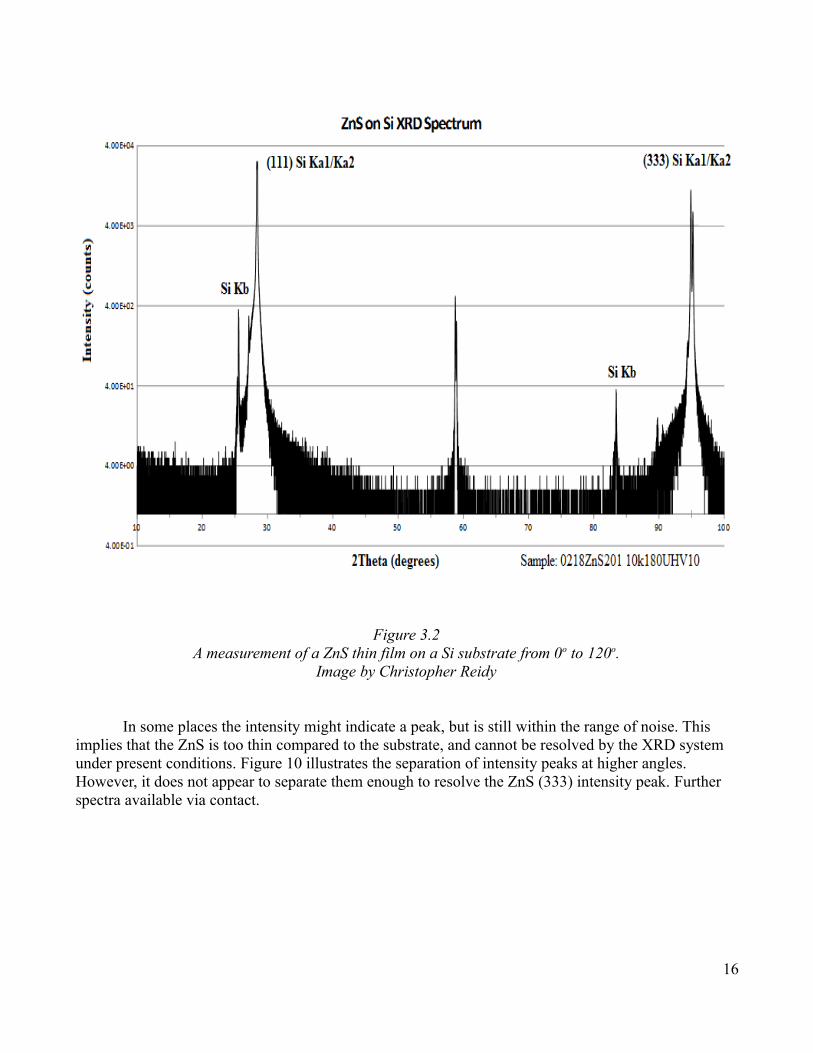
Figure 3.2A measurement of a ZnS thin film on a Si substrate from 0o to 120o.
Image by Christopher Reidy
In some places the intensity might indicate a peak, but is still within the range of noise. This implies that the ZnS is too thin compared to the substrate, and cannot be resolved by the XRD system under present conditions. Figure 10 illustrates the separation of intensity peaks at higher angles. However, it does not appear to separate them enough to resolve the ZnS (333) intensity peak. Further spectra available via contact.
16

Conclusions
The lack of resolution is likely due to the burying of ZnS peaks in the massive Si signal, rather than the peaks being non-existent. On a thinner substrate, or with a thicker ZnS layer, detection of ZnS peaks should be possible. It is probable that XRD will not provide the resolution needed to detect the ZnS thin film, or examine its properties. However, it is a very useful method for determining whether the sample is single or polycrystalline, since peaks from misaligned ZnS lattice planes will still appear. This reduces the number of samples sent to be examined with tunneling electron microscopy, and overall saving large amounts of time. While other materials such as oxygen may be present in a sample, their quantities are so low that the lattice is effectively single crystal.
The Si was (111) oriented as shown by both TEM and XRD, as was the ZnS thin film on its surface. This implies that the ZnS peaks were simply buried, rather than appearing in the wrong place due to being polycrystalline or having a different orientation.
17

References
1. Cullity, B. D., and S R. Stock. Elements of X-ray Diffraction. 3rd ed. Reading, MA: Addison-Wesley Publishing company, Print.
2. Robinson, I K. "Surface X-ray Diffraction." 55.5 (1992): 599-691. Web of Science. http://iopscience.iop.org/0034-4885/55/5/002. Web. 23 Oct. 2012.
3. “Bragg's law” Wikipedia: The Free Encyclopedia. Wikimedia Foundation, Inc., date last updated (20 April 2013). Web. Date accessed (5 March 2013). <http://en.wikipedia.org/wiki/Bragg%27s_law>
4. “Miller Index” Wikipedia: The Free Encyclopedia. Wikimedia Foundation, Inc., date last updated (24 March 2013). Web. Date accessed (02 April 2013). <http://en.wikipedia.org/wiki/Miller_index>
18