
Details of the Philips Hue Smart Lighting...
48
Colin O’Flynn 1 A LIGHTBULB WORM? Details of the Philips Hue Smart Lighting Design Colin O’Flynn – August 1, 2016. (Black Hat USA 2016 White Paper) ABSTRACT This whitepaper is designed to show some details of the Philips Hue system. It is not designed to demonstrate any specific attack, but instead a chance to “poke around” to see what security features are present. It is designed to serve as a reference for those designing similar systems, to give an idea what attack surfaces might be exploited. This analysis focuses on the embedded hardware itself. In particular, I look at the Bridge 1.0 (round), the Bridge 2.0 (square), the low-cost white light bulbs, and the BR30 color bulb. The newer Bridge 2.0 makes an interesting target for hardware hackers to use, as it’s possible to obtain a root console (as discussed herein) allowing you to take control of this device. Having access to the root console also allows more detailed analysis of the binaries present on the bridge, which could lead to the discovery of other vulnerabilities. In particular, the are some ‘interesting’ files including what appears to be a master process for running the Bridge 2.0 (webserver, certain aspects of ZigBee, talking to Hue app, etc.). Overall, we still find a number of security features present on the various systems that make it more difficult to attack than typical consumer electronics. Firmware updates appear always to be encrypted to protect them from analysis, and are signed to protect devices from being reprogrammed by another actor. Despite this, certain engineering trade-offs may cause problems in the future. Bulbs of the same type use the same encryption key for the firmware files, which means that a leak of that encryption key could allow someone to permanently reprogram lightbulbs over the air. This could cause a variety of problems, in the extreme case allowing a reflashed bulb to then reflash nearby bulbs (i.e., a worm). This work came about due to attempting to answer someone’s question about the possibility of a lightbulb worm (hence the title, with the question mark).
-
Upload
duongtuyen -
Category
Documents
-
view
217 -
download
0
Transcript of Details of the Philips Hue Smart Lighting...

Colin O’Flynn
1
A LIGHTBULB WORM? Details of the Philips Hue Smart Lighting Design
Colin O’Flynn – August 1, 2016.
(Black Hat USA 2016 White Paper)
ABSTRACT
This whitepaper is designed to show some details of the Philips Hue system. It is not
designed to demonstrate any specific attack, but instead a chance to “poke around” to see
what security features are present. It is designed to serve as a reference for those designing
similar systems, to give an idea what attack surfaces might be exploited.
This analysis focuses on the embedded hardware itself. In particular, I look at the Bridge
1.0 (round), the Bridge 2.0 (square), the low-cost white light bulbs, and the BR30 color bulb.
The newer Bridge 2.0 makes an interesting target for hardware hackers to use, as it’s
possible to obtain a root console (as discussed herein) allowing you to take control of this
device.
Having access to the root console also allows more detailed analysis of the binaries present
on the bridge, which could lead to the discovery of other vulnerabilities. In particular, the
are some ‘interesting’ files including what appears to be a master process for running the
Bridge 2.0 (webserver, certain aspects of ZigBee, talking to Hue app, etc.).
Overall, we still find a number of security features present on the various systems that
make it more difficult to attack than typical consumer electronics. Firmware updates
appear always to be encrypted to protect them from analysis, and are signed to protect
devices from being reprogrammed by another actor.
Despite this, certain engineering trade-offs may cause problems in the future. Bulbs of the
same type use the same encryption key for the firmware files, which means that a leak of
that encryption key could allow someone to permanently reprogram lightbulbs over the air.
This could cause a variety of problems, in the extreme case allowing a reflashed bulb to
then reflash nearby bulbs (i.e., a worm).
This work came about due to attempting to answer someone’s question about the possibility
of a lightbulb worm (hence the title, with the question mark).

Colin O’Flynn
2
1 INTRODUCTION
The Philips Hue is one of the most popular “smart lighting” products on the market. If you
haven’t used these devices, the idea of a “smart lightbulb” might seem like another dumb
internet of things example, there are many practical uses that have driven its adoption.
For example, using these smart light bulbs allows you to “rewire” switch layouts. A simple
wall-mount switch (which requires no batteries, as it is powered by a minute amount of
mechanical energy you generate by hitting the switch) means you are not constrained by
how your house is currently wired, or even placement of the switch. Anyone who has
struggled with a switch that is half-hidden behind a piece of furniture will appreciate such
abilities!
Of course many more advanced uses are possible, such as automatically adjusting lighting
based on other devices turning on, remotely controlling lights, linking light settings to
motion detection, etc.
The Philips Hue is built on top of the ZigBee Light Link (ZLL) protocol; you can see more
about this from the ZigBee Alliance website at http://www.zigbee.org/zigbee-for-
developers/applicationstandards/zigbee-light-link/ . You can also download details from
some of the silicon manufacturers that make devices for ZLL networks – for example, NXP
has a PDF at http://www.nxp.com/documents/user_manual/JN-UG-3091.pdf, which goes
through details of the ZLL.
ZigBee itself is built on top of a low-power radio network called IEEE 802.15.4. This
standard is designed for very low-power, low data rate devices. The maximum packet size is
127 bytes and maximum transfer rate is 250 kbit/s. Range varies somewhat based on
conditions & specifics of the radios – about 25-100m is typical for IEEE 802.15.4 devices in
practical scenarios.
It is possible to achieve ranges of over a 1000m line-of-sight with some IEEE 802.15.4
devices using the standard antennas (i.e., NOT Yagi or high-gain antennas).
ZigBee is commonly run at the 2.4 GHz band (in the same band as Wi-Fi), although there is
a lower-frequency version that can occupy a band around 700-900 MHz (specific band
depends on region of the world). The ZLL runs entirely on the 2.4 GHz band, thus range
may also depend on how much traffic the ZLL network needs to conflict with.
The central node in these networks is called the “bridge” by Philips, as it controls all the
light-bulbs. This bridge device contains the IP link as well, typically via an Ethernet jack.
The bridge devices powers up and makes a network, which the various lightbulbs can then
join.
Colin O’Flynn
3
ZLL SECURITY TRADE-OFFS
One of the most difficult problems for these types of devices is how to securely “join” an
authorized network.
If you bring home a smart light, how does it know what network to join, and how does it do
so securely? The IEEE 802.15.4 radio chips (these chips form the basis of any ZigBee device,
be ZLL or otherwise) almost always have support for AES-128 which is used to encrypt
network traffic. In ZLL there is a network-wide key used for all traffic.
Such a network-wide key is very common in these types of networks; few protocols use
different link keys between devices. But how you give the new device that network key is
critical – we obviously cannot send it in cleartext, in case an attacker is listening.
And some devices (such as the wall-switches) may be so power-constrained they cannot
perform much processing beyond simply sending messages. Anything that uses asymmetric
cryptography or a D-H key exchange is infeasible.
ZLL solves the problem through the use of a master (symmetric) key. This master key is
used to encrypt a network key, which can then be securely sent to a device joining the
network. Anyone making a ZLL device knows this master key, and promises to store it
securely.
This ZLL master key would also be programmed into every ZLL device – if even one
customer had one insecure product that revealed the key, it is no longer considered a secret.
However – all may not be lost. Even if an attacker has the key, they cannot automatically
determine the network key for a given random network. They would have to join that
network or observe the traffic of another device joining.
An attacker may, however, be able to perform a “Light Stealing” attack. There is a provision
within the ZLL to remotely request that a device is “reset to factory new” state. If an
attacker was in possession of the ZLL master key, they could send such legitimate requests.
To help combat this, devices perform verification based on the received signal strength
indicator (RSSI) of such requests. Devices are only supposed to respond if the signal is
sufficiently strong to indicate it comes from a nearby device – in the case of Philips Hue, it
appears to only works if approximately 30 cm away.
In legitimate requests, the transmit power is also lowered. As an attacker we would have no
such issues, and can use excessive transmit power for sending these requests. Such a
request format may allow nearby attackers to temporarily “take over” lights by forcing
them to join a new network. More detail on this will be published in a forthcoming paper by
another author (with some details/demos at Blackhat USA 2016).
Ultimately, while you may be surprised by the use of a fixed symmetric master key, given
the various constraints it provides a reasonable trade-off between a secure implementation

Colin O’Flynn
4
and good “out of box” experience, which is supposed to allow different manufactures even to
work together.
There are a number of assumptions underlying this of course (mainly about the correctness
of certain implementations), and we’ll explore some of these here.
2 PREVIOUS & FUTURE WORK
I’m far from the first person to look at ZigBee, ZLL, or even the Philips Hue system. I
thought I’d provide a few links for information that will be of interest to you.
Travis Goodspeed has done considerable work in ZigBee hacking:
See one of his Blackhat presentations: https://www.blackhat.com/presentations/bh-
usa-09/GOODSPEED/BHUSA09-Goodspeed-ZigbeeChips-SLIDES.pdf
Other older work published on his blog too, see for example:
http://travisgoodspeed.blogspot.ca/2009/03/breaking-802154-aes128-by-syringe.html
Which references some associated interesting
Tobias Zillner’s ZigBee Exploited talk & white-paper also is a good quick introduction:
Slides link: https://www.blackhat.com/docs/us-15/materials/us-15-Zillner-ZigBee-
Exploited-The-Good-The-Bad-And-The-Ugly.pdf
Whitepaper link: https://www.blackhat.com/docs/us-15/materials/us-15-Zillner-
ZigBee-Exploited-The-Good-The-Bad-And-The-Ugly-wp.pdf
There are many more people working on hacking ZigBee/IEEE 802.15.4 networks. For
example the KillerBee framework (published by
http://www.riverloopsecurity.com/projects.html) is a good example of how advanced tools
can be!
Nitesh Dhanjani has specifically done work on the Philips Hue system:
A 46-page paper is available at
http://www.dhanjani.com/docs/Hacking%20Lighbulbs%20Hue%20Dhanjani%202013.
The last referenced paper (Nitesh Dhanjani) goes into considerable detail on protocol-layer
flaws in the Philips Hue system looking at traffic to/from the bridge device. My work has
concentrated only at attacks starting at the bridge and beyond (i.e., no work was done by
me on the network traffic).
While I don’t know the source, the ZLL master key I mentioned earlier appears to be
leaked, showing up in various online sources. It’s thus possible an attacker could either (a)
perform attacks that require talking to ZLL devices, or (b) impersonate a ZLL device by
being able to decrypt and determine a ZLL link key. This was reported by Tobias Zillner in
his “Zigbee Exploited” talk as well.

Colin O’Flynn
5
Also, during my preparation for this work I met another researcher, Eyal Ronen, who has
been working hard on similar security analysis, but going much more in-depth on the
actual firmware update process along with what is required to reflash arbitrary bulbs over
the air (OTA).
Eyal previously published a paper demonstrating what could happen should an attacker
take control of your bulbs – in particular using them to leak data by bulb brightness
changes (see http://www.wisdom.weizmann.ac.il/~eyalro/EyalShamirLed.pdf for this paper).
While at the time I’m writing this whitepaper for Black Hat 2016 his newer research is not
yet released, I highly recommend checking his website at
http://www.wisdom.weizmann.ac.il/~eyalro/ for updates. His work looks to (a) release
specific attacks again some of these devices, and (b) push these attacks to be useful in
complex and realistic scenarios. It’s also ongoing, so he’ll likely have more attacks in the
future too!
3 USEFUL TOOLS
The objective of this work is to show what type of hacks are possible. The specifics of tools
required depends on what you wish to accomplish. To accomplish the rooting requires the
minimal amounts of tools:
USB to Serial adapter.
A few paperclips (or some bits of wire).
But for more advanced hacks, you’ll start to need additional tools such as:
Bus pirate (SPI flash dumping).
Volt meter.
Oscilloscope.
Fine-tipped soldering iron (I love the Metcal ones).
Stereo microscope for inspecting/soldering.
To do the power analysis & glitching attacks, I also used:
ChipWhisperer Capture hardware (ChipWhisperer-Pro was used here, but most of
the attacks possible with ChipWhisperer-Lite + some external logic for triggering).
With that background, let’s dive right into some specific examples of the hardware. I’ll start
with the older version of the bridge device.
4 BRIDGE V 1.0
The “bridge v1.0” are the original version of the Hue bridge, which are round in appearance.
The internals of the bridge are shown below:
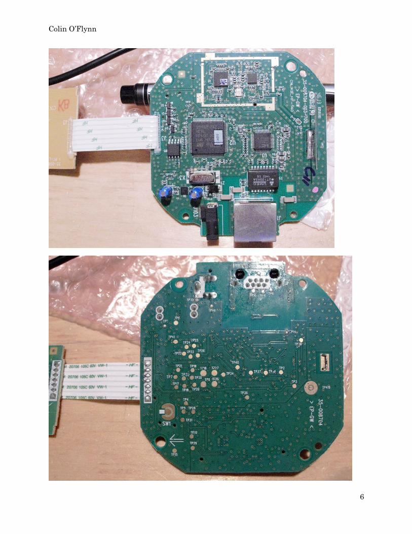
Colin O’Flynn
6

Colin O’Flynn
7
These bridges contain two sections: the main ARM processor, and the Zigbee ZLL solution
(referred to as the ‘Zigbee SoC’. The use of a separate chip for holding the entire ZigBee
stack is something we’ll see repeated in the second-generation bridge as well.
The main ARM processor is a STM32F217VET6 by ST (direct link to datasheet:
http://www.st.com/content/ccc/resource/technical/document/datasheet/51/9b/66/ba/d4/a8/49/4
a/CD00263874.pdf/files/CD00263874.pdf/jcr:content/translations/en.CD00263874.pdf) .
This is a Cortex M3 device, with 512 Kbyte FLASH memory (internal) + 128Kbytes of
SRAM (internal). It contains a number of cryptographic hardware accelerators (AES +
3DES + MD5 + SHA-1).
There is an external SPI flash chip (Winbond 25Q16BVS) connected to the ARM processor.
On a virgin bridge this appears to hold simple strings indicating the ZLL groups and
similar information, but is almost entirely filled with “FF” bytes (i.e., empty):
Once a bridge has been running, it holds additional configuration information. It does not
appear to ever hold an unencrypted firmware update, even during the update process itself
(more details later on that).
The ZigBee section is of most interest to us. It contains a CC2530F256 IEEE 802.15.4 SoC
device, alongside a CC2590 “range extender” (i.e., amplifier). There are a number of test
points on the PCB, so I can briefly talk about their purpose in our “first look” at the bridge
device.
BRIDGE DEVICE – FINDING SERIAL PORTS
To get an idea of the boot process, we can find 3 serial ports on the PCB which spit data out
at a standard 115,200 baud rate. One is connected to the ARM (status information), and
two are the link between the CC2530 and the ARM. These test points are marked on the
bottom as:
TP30 is the ARM serial log output

Colin O’Flynn
8
TP9/TP10 is the CC2530 to ARM serial port test points
An example of the communication between the ARM and the CC2530 is given below.
Data to ARM from CC2530:
[Log,Info,S_DeviceInfo,Booting into normal mode...]
[Log,Info,S_DeviceInfo,DeviceId: IpBridge]
[Log,Info,N_Security,LIB4.4.52]
[Log,Info,N_Security,KeyBitMask,0x0012]
[Log,Info,A_Bridge,Platform version 0.25.0,package_ZigBee
8720,package_Z_Stack 8720,built by LouvreZLL]
[Log,Info,A_Bridge,Product version 5.7.1,SmartBridge 11393,built by
LouvreZLL]
[Bridge,Version,5.7.1,SmartBridge 11393,built by LouvreZLL]
[Bridge,GroupRange,0x5357,0x5367]
[Log,Info,D_Led,dc 16]
[Bridge,NetworkSettings,False,0xB163,26DF52A183D85889,11,0,S=0x0001]
[Log,Info,A_Bridge,NwkAddr: 0x0001, Ch: 11, Pan: 0xB163, NwkUpdId: 0,
ExtPanID:26:DF:52:A1:83:D8:58:89]
[Log,Info,D_Led,dc 16]
[TH,Ready,0]
[Connection,A]
[Connection,GetAddress,L=00:17:88:01:01:07:BF:FC,S=0x0001.0]
[Bridge,StoreGroupRange,0]
[Log,Info,N_ConnectionRouter,Startup network discovery...]
Data to CC2530 from ARM:
[Link,A]
[Link,GetAddress,L=00:17:88:01:01:07:BF:FC,S=0x0001.0]
We can see the general format of requests being sent as [Module, Request1<, Request 2>]
and responses being [Module, Response1 <,Response2>]. Specifics of the number of
arguments seems to vary between parameters.
BRIDGE DEVICE – TAKING OVER SERIAL
The Zigbee SoC contains the secret ZLL encryption key. An interesting attack is that we
never actually need to determine this key, but can instead use the provided Zigbee SoC to
send and receive messages that will be encrypted with the correct key. This attack would be
made more powerful by looking at the Bridge 2.0 device, where we can find more details of
the communications protocol encoded inside a control application.
I’ll demonstrate the data format later when looking at the over-the-air update for the BR30
bulb.

Colin O’Flynn
9
FIRMWARE UPDATE: NETWORK PERSPECTIVE
It’s relatively easy to monitor the network traffic while performing a firmware update. This
details there is a server which simply provides a file that is downloaded, this file has a
name like
firmware_rel_cc2530_encrypted_stm32_encrypted_01030262_0012.fw . As
suggested by the name, it includes both the firmware for the CC2530 and for the STM32
processor.
Both appear to be encrypted (no noticeable strings, etc). It’s easy to get different releases of
this file, and comparing them shows the encryption does not appear to be something like a
stream cipher using the same key, as we would expect runs of the same encrypted
sequences where code aligned between them (such as the value of strings, init code, etc.).
Our primary interest at this point is the ZigBee side, so will concentrate on how the
CC2530 firmware update works. I’ll discuss that next.
FIRMWARE UPDATE: CC2530
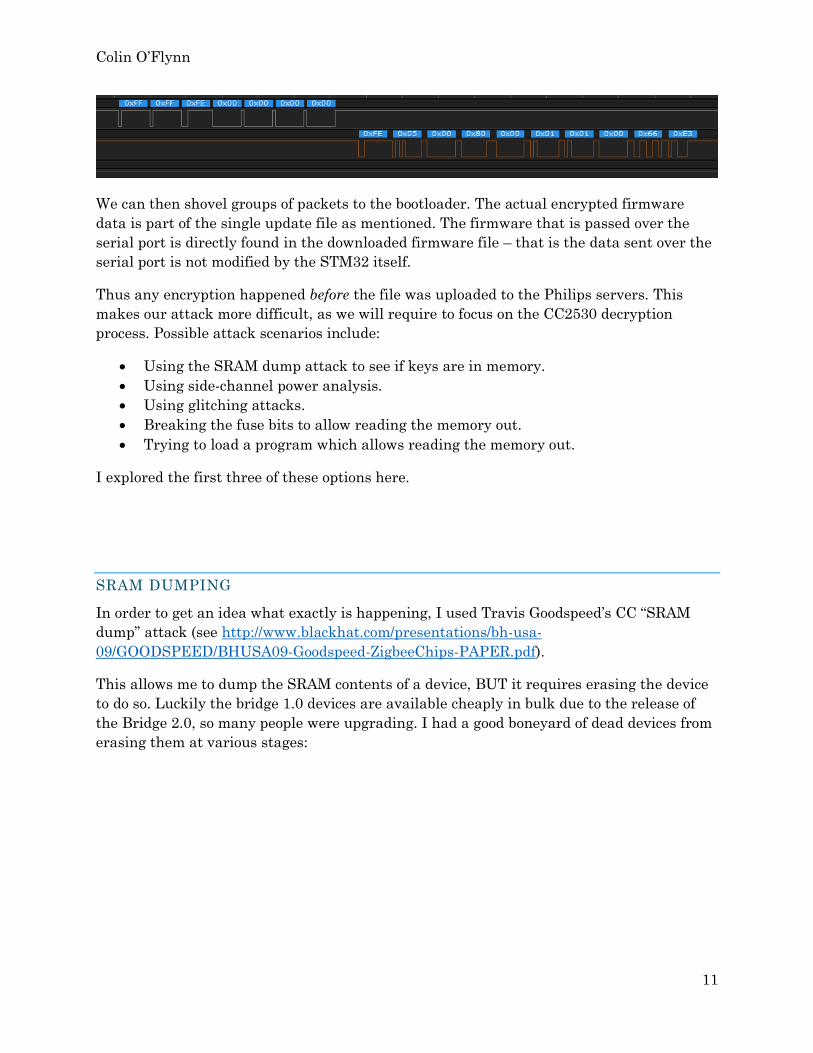
Using a Logic Pro 16, I could log the entire serial protocol during the update process to see
what happens during this process. It took a little while to perform the complete update, as
can be seen here:
We can look closer, and see “gaps” between groups of packets:
Each of those “Gaps” represents the delay of a page erase. Zooming in closer you can see
there is 32 packets, each packet containing 64 bytes of data between page erases:

Colin O’Flynn
10
This 2048 byte spacing aligns with the actual page size of the CC2530. Looking at the
bootloader protocol, we can determine it appears to be an implementation of the
“SerialBootLoader” (see http://processors.wiki.ti.com/index.php/SerialBootLoader for
command list).
An example SBL implementation with encryption is available at https://github.com/lee-
wei/CC2540/tree/master/Projects/ble/util/EBL/app, which is a version for the CC2540. The
file format appears to differ from this project, but it provides a useful starting point to
understand a possible code flow.
The frame format is fairly simple, with 6 bytes of header:
FE is the “start of frame” header.
42 is the length (66 bytes, payload + addr)
00 01 is a fixed sequence
02 00 is the page to write (in LSB, MSB format, so this equates to 0x0002)
Next follows 64 bytes of (encrypted) data.
Finally a FCS byte is calculated as the XOR of the previous bytes (see the SBL
documentation for details).
If the message is OK (FCS passes + the expected address was sent), the bootloader response
with an OK command. At this point the next frame can be sent:
To enter bootloader mode, pin P0.1 was determined to be responsible for entering
bootloader mode. If this pin is pulled HIGH after a reset, the bootloader will be entered. If
the pin is LOW, the regular code will run. Assuming we entered the bootloader, we can
send the “sign-on” command, FF FF FE 00 00 00 00. The bootloader will respond with
FE 05 00 80 00 01 01 00 66 E3:
Colin O’Flynn
11
We can then shovel groups of packets to the bootloader. The actual encrypted firmware
data is part of the single update file as mentioned. The firmware that is passed over the
serial port is directly found in the downloaded firmware file – that is the data sent over the
serial port is not modified by the STM32 itself.
Thus any encryption happened before the file was uploaded to the Philips servers. This
makes our attack more difficult, as we will require to focus on the CC2530 decryption
process. Possible attack scenarios include:
Using the SRAM dump attack to see if keys are in memory.
Using side-channel power analysis.
Using glitching attacks.
Breaking the fuse bits to allow reading the memory out.
Trying to load a program which allows reading the memory out.
I explored the first three of these options here.
SRAM DUMPING
In order to get an idea what exactly is happening, I used Travis Goodspeed’s CC “SRAM
dump” attack (see http://www.blackhat.com/presentations/bh-usa-
09/GOODSPEED/BHUSA09-Goodspeed-ZigbeeChips-PAPER.pdf).
This allows me to dump the SRAM contents of a device, BUT it requires erasing the device
to do so. Luckily the bridge 1.0 devices are available cheaply in bulk due to the release of
the Bridge 2.0, so many people were upgrading. I had a good boneyard of dead devices from
erasing them at various stages:

Colin O’Flynn
12
The debug pins are at TP29/TP31 for DD/DC respectively. You also need the reset pin at
TP28. Note the reset pin is driven by the STM32 by default – you can either try holding the
STM32 in reset itself to float the pin, or cut the reset by lifting a resistor and instead
driving the reset pin from there, as I have done:
I erased several devices at various stages, such as:
When running normally (not in the bootloader).
At various stages of the bootloader – before receiving any data, after receiving the
first valid frame, second valid frame, and a “much later” frame.
The following shows a dump comparing two such locations – here is the difference between
the first valid frame, and after the second valid frame:

Colin O’Flynn
13
Note the messages from address 0xA1 to 0xA6 is the TX buffer (that was the FE 01 00 81
00 80 that was sent in response to an accepted packet). The part after that is the received
data, suggesting this is the RX buffer.
I was hoping the data was decrypted in-place and left in SRAM, but it appears that the
bootloader is overwriting memory once done with it. This is suggested by the block of FF in
place of the RX buffer – it’s assumed that perhaps the first frame didn’t include any
encrypted data, but was instead setup information, the expected signature, etc.

Colin O’Flynn
14
In addition, I didn’t find any keys that appeared to decrypt the firmware file. This required
some guesses on my part – for example I didn’t try AES-CTR mode decryption, I was only
using AES-CBC with various key sizes & byte orders.
The known ZLL master key also did not appear in any of the SRAM dumps (including
dumps when the device was running normally, not in bootloader mode).
This suggests Philips was aware of this attack vector, and rather actively worked to avoid
leaving sensitive data in memory. This attack was published in 2009, so we would hope the
designers were aware of it, and avoided keeping sensitive data in SRAM when not needed.
While the data is presumably still in memory at some point, it would require very precise
timing to recover this data. In addition, it would come at a large cost in terms of number of
bridge devices killed.
For the bootloader at least, we can avoid needing so many bridges by taking advantage of
glitch attacks.
GLITCH ATTACKS
Rather than erasing the device, we can use clock glitching to dump the buffer (see
http://wiki.newae.com/Tutorial_A7_Glitch_Buffer_Attacks for a tutorial). This is possible
because there is likely some transmit code like the following:
for(uint8 i = 0; i < data_to_send; i++){
uart_write(tx_buf[i]);
}
We can use a glitch attack to cause this loop to send more data than expected, which will
send the RX buffer back to us. This works because the RX buffer is located in memory after
the TX buffer. Causing the above transmit loop to execute additional iterations will simply
transmit the memory beyond the TX buffer.
If this RX buffer now contains decrypted data, it would also be sent to us. This was
successful in that it allowed reading out the RX buffer, as the following shows:

Colin O’Flynn
15
This used a clock glitch inserted after receiving the correct response. This caused the
system to continue sending data back to me, and allowed recovery of the complete RX buffer
(along with some memory beyond that buffer).
At this point I haven’t determined the timing for reading the decrypted data – the data
appears to have been wiped by the time the glitches cause the data to be read back. Further
work is required, such as inserting glitches to avoid wiping the memory.
Because the ZLL master key is already known, getting the decrypted bridge firmware may
not be of great value. It’s still possible there could be bugs in the bridge interface we wish to
exploit, but I haven’t pushed further in this area.
SIDE-CHANNEL POWER ANALYSIS
Side-channel power analysis is another potential method of retrieving the encryption key. I
designed a custom board for both side-channel power analysis and the glitching attacks, on
which I mounted a CC2530 extracted from a bridge device:

Colin O’Flynn
16
Using the known protocol, I could cause this device to perform the bootloading process (and
thus perform the decryption operation).
Based on the timing, it seemed likely the AES hardware accelerator in the CC2530 is used.
At this point the CC2530 hardware accelerator has not been broken, so performing side-
channel power analysis would first require breaking the hardware accelerator in the ideal
case.
This would entail a time commitment beyond what would be required to move my work
(and answer the question in the general case) forward.

Colin O’Flynn
17
Given enough time I think one of the above attacks looks likely to succeed, but they are not
trivial to get either the timing or the measurements working. Instead I’ll move onto the
newer bridge devices, which have a more interesting architecture.
5 BRIDGE V 2.0
The top and bottom side of the bridge is shown below:

Colin O’Flynn
18
The bridge itself has a QCA4531 main SoC, which is a MIPS processor by Qualcomm. It’s
designed for these “internet of things” type environments.
There is DDR memory associated with it, alongside a 1GBit SPI-connected NAND flash P/N
GigaDevice GD5F1GQ4UC (datasheet: http://gigadevice.com/product/download/242.html ),
and a smaller SPI-connected NOR flash (this is the standard type of SPI flash), P/N
25Q41BT.
The two flash memories are present because the smaller SPI flash contains the bootloader.
This is loaded first, and then the larger flash memory is used to load the kernel &
filesystem.

Colin O’Flynn
19
For the ZigBee connection, an Atmel SAMR21E18A is provided. This is a very low-power
Cortex-M0+ ARM processor that also has an IEEE 802.15.4 radio built in. Once again it has
a small SPI flash memory connected, presumably for the purpose of storing various ZigBee
information.
The connection between the SAMR21E18A and the QCA4531 is mostly done through a USB
to Serial chip, a PL2303SA mounted at SU7. In addition, there is a buffer at SU8 which
holds the SAMR21 in reset until the QCA4531 is ready. This buffer is assumed present
because the input appears to be 2.5V logic, and the output a 3.3V logic. The test pad at
TP34 allows an override of this logic, to avoid waiting for the QCA4531 to boot. You can also
lift the pad of SU8 that connects to the reset pin of the SAMR21 (this is what I did).
The SAMR21 reset is not a labeled test point. The TX/RX pair is at TP14 and a nearby
unnamed test point. All of these are shown below:
The additional connections labeled “power analysis” and “CLK-IN” are used for performing
side-channel power analysis (more on this later).
The SAMR21 has a programming heading at J7, which can be mounted as it uses a
standard Atmel 0.05” spacing 10-pin header. Even with this header mounted the chip did
not respond to programming commands. The reset pin was wired to the header for this test
(by default only the SWDIO and SWCLK pins were wired to the header), and the pin from
SU8 was lifted to avoid driving the reset pin during these attempts.
For the QCA4531 I didn’t find a test point with an easy “reset” pin. This is useful as holding
the main QCA4531 chip in reset was needed during analysis of the SAMR21 without

Colin O’Flynn
20
removing it from the board. As the SAMR21 reset pin is driven by a buffer, it still required
lifting the reset pin, as mentioned previously.
Instead, I determined there appeared to be a pin that when pulled low caused a reset to
happen. This was found by probing with a 1K resistor to ground – this should be
sufficiently strong to pull down a logic pin, but without shorting out other pins.
I don’t know if the pin is actually reset or something else (a test pin, shutdown pin, etc) but
it “did the trick”. In particular, power consumption was much lower when this pin was held
down, indicating processing was not occurring. This pin connection is shown below, the top
part of this photo is near the edge of the PCB:
Considerable mechanical support is required here – the “pin” is actually a small amount of
exposed metal, as the actual connection is underneath the chip. I couldn’t find anywhere
this pin connects to on the board which would have been an easier test point. Not shown in
the photo is a large blob of glue placed over this connection, and the wire is wrapped around
a hole in the PCB to give it more mechanical support.
BRIDGE DEVICE – FINDING SERIAL PORTS
Finding serial ports is again done with probing around using an oscilloscope to look for
interesting traffic after a boot.
The serial port for the ZigBee SoC was discussed above, and the serial port for the main
QCA4531 will be discussed below. Note the traffic on the ZigBee SoC took some time to
happen after a reboot (~30 – 60 seconds), as the ZigBee SoC is held in reset by the
QCA4531 until it fully boots up.
Colin O’Flynn
21
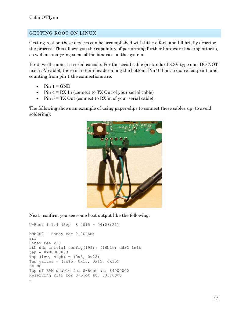
GETTING ROOT ON LINUX
Getting root on these devices can be accomplished with little effort, and I’ll briefly describe
the process. This allows you the capability of performing further hardware hacking attacks,
as well as analyzing some of the binaries on the system.
First, we’ll connect a serial console. For the serial cable (a standard 3.3V type one, DO NOT
use a 5V cable), there is a 6-pin header along the bottom. Pin ‘1’ has a square footprint, and
counting from pin 1 the connections are:
Pin 1 = GND
Pin 4 = RX In (connect to TX Out of your serial cable)
Pin 5 = TX Out (connect to RX in of your serial cable).
The following shows an example of using paper-clips to connect these cables up (to avoid
soldering):
Next, confirm you see some boot output like the following:
U-Boot 1.1.4 (Sep 8 2015 - 04:08:21)
bsb002 - Honey Bee 2.0DRAM:
sri
Honey Bee 2.0
ath_ddr_initial_config(195): (16bit) ddr2 init
tap = 0x00000003
Tap (low, high) = (0x8, 0x22)
Tap values = (0x15, 0x15, 0x15, 0x15)
64 MB
Top of RAM usable for U-Boot at: 84000000
Reserving 214k for U-Boot at: 83fc8000
…
Colin O’Flynn
22
What we need to do is short a test-point on the NAND SPI flash during the boot process.
This must occur right after the following is printed to the serial port (roughly):
Net: ath_gmac_enet_initialize...
Fetching MAC Address from 0x83febe80
Fetching MAC Address from 0x83febe80
ath_gmac_enet_initialize: reset mask:c02200
Scorpion ---->S27 PHY*
S27 reg init
: cfg1 0x800c0000 cfg2 0x7114
eth0: 00:03:7f:11:20:ce
athrs27_phy_setup ATHR_PHY_CONTROL 4 :1000
athrs27_phy_setup ATHR_PHY_SPEC_STAUS 4 :10
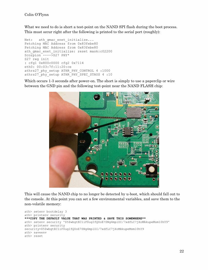
Which occurs 1-3 seconds after power-on. The short is simply to use a paperclip or wire
between the GND pin and the following test-point near the NAND FLASH chip:
This will cause the NAND chip to no longer be detected by u-boot, which should fall out to
the console. At this point you can set a few environmental variables, and save them to the
non-volatile memory:
ath> setenv bootdelay 3
ath> printenv security
***COPY THE DEFAULT VALUE THAT WAS PRINTED & SAVE THIS SOMEWHERE**
ath> setenv security '$5$wbgtEC1iF$ugIfQUoE7SNg4mplDI/7xdfLC7jXoMAkupeMsm10hY9'
ath> printenv security
security=$5$wbgtEC1iF$ugIfQUoE7SNg4mplDI/7xdfLC7jXoMAkupeMsm10hY9
ath> saveenv
ath> reset

Colin O’Flynn
23
The first one is simply making it possible to hit “enter” on the serial port during boot to fall
into the bootloader menu. This means you only need to perform the NAND flash trick once,
then not worry about doing it again, even if you want to modify other strings in the u-boot
menu.
The second is writing a new root password. Before doing that you should save the old
password. These are in the shadow-file format, and you can use ‘mkpasswd’ to generate
your own.
The given example results in a root password of ‘toor’. Once the device resets, you should be
able to log in with root/toor and receive a prompt. This will happen after the device fully
boots, and you can press “enter” to receive the log-in prompt. You can see a video of this
being performed at https://www.youtube.com/watch?v=hi2D2MnwiGM .
At this point, you’ll want to edit the file /etc/rc.local and add the following to enable telnet:
iptables -I INPUT -p tcp --dport 23 --syn -j ACCEPT
telnetd
You may also want to add the /etc/rc.local to the /etc/sysupgrade.conf file to avoid it being
overwritten in the future.
Before powering off the system, use the ‘halt’ command. This will cause data to be written
to the flash memory (otherwise it may be lost). Use the halt command and then power-cycle
the device to reset it. If you fail to do this the changes to rc.local might not be written to
flash and the daemon won’t come up.
Once the system comes up again, you should be able to telnet in! You’ll need to know the IP
address, which you can either get via the Hue App, or using ‘ifconfig’ on the serial console,
or by checking your DHCP tables in your router.
You can also try pinging Philips-hue.local which should resolve to the IP address of
your bridge (this won’t work on Windows 7 by default, but will on Linux / Mac OSX and
perhaps Windows 10).
GETTING A MASTER SHELL
While the above trick is the best option for getting a useful root shell, I originally used u-
boot to modify the ‘init’ argument of the kernel. This was done with the following:
setenv std_bootargs 'board=BSB002 console=ttyS0,115200 ubi.mtd=overlay
rootfs=/dev/mtdblock:rootfs rootfstype=squashfs noinitrd
init=/bin/sh';
Where the default would be:

Colin O’Flynn
24
setenv std_bootargs 'board=BSB002 console=ttyS0,115200 ubi.mtd=overlay
rootfs=/dev/mtdblock:rootfs rootfstype=squashfs noinitrd
init=/sbin/init';
By calling /bin/sh, the system falls into a root shell on boot. However it does not run the
‘init’ binary, which causes a lot of problems. In particular the filesystem remains read-only,
and a number of entries are not populated (such as the /proc filesystem).
However the /bin/sh shell is powerful as it did not require me to know anything about how
the ‘security’ envvar was used. Instead I determined later that it was being copied into the
shadow file, and thus was the root password.
INTERESTING FILES AND NOTES
There are many interesting files available which can be further studied:
The main function of the router seems to be held in a binary called ‘ipbridge’ at
/usr/sbin. This seems to be the most likely location to find flaws. This binary appears
to be everything from the webserver (including having the HTML pages encoded
inside it) to handling ZigBee events to parsing requests.
The `ipbridge_io’ in particular talks with the Zigbee SoC, meaning this binary in
combination with ‘ipbridge’ could tell us:
o What commands are used by the SoC (so we can use the SoC ourselves).
o Are there any bugs allowing the SoC to send messages which cause problems,
potentially allowing an attacker that was able to send some messages to the
Linux system over the zigbee link to cause problems for the bridge?
There is a file at /home/swupdate/certs/enc.k, which you can use “hexdump” to see
contains 32-bytes of data. This file is referenced from /usr/sbin/swupdate as being
the AES-256-CBC key used in decrypting certain binary blobs during the SW update
process.
This key is constant across the two different Hue Bridges I looked at. This key,
however, only decrypts some data store, that data store itself still has an encrypted
firmware image for the Zigbee SoC inside it.
The binary ‘zigbee_soc_updater’ at /usr/sbin which appears to handle the bootloading
process for the SoC. This may have additional information about the blob format, as
it seems to reference both a HwId and a KeyId being encoded in the binary blob.
Colin O’Flynn
25
The zigbee SoC firmware files themselves seem to be placed at /lib/firmware – again
these are the encrypted SBL files, so this isn’t a huge attack.
Looking at two different devices, they appeared to have different root passwords. I’ve
been told devices have unique root passwords per device, which is a definite win
security-wise.
FIRMWARE UPDATE – NETWORK PERSPECTIVE
One of the first things I did was sniff the network traffic while performing a firmware
update. This revealed a single binary blob was downloaded, called
bsb002_image_01032318.fw2. This file once again appears to be encrypted, and unlike
last time was not simply split into two files, where one is sent to the Zigbee SoC directly.
None of the sequences sent to the SoC over the serial port appeared in this binary file at all.
Having now looked at the swupdate binary, it’s clear this is because the encrypted Zigbee
SoC firmware file is further encrypted inside the update image. The update image does
have a signature present, and presumably, this is checked by the Bridge itself to avoid
loading unsigned binaries. The combination of encryption & signing should stop an attacker
from forcing someone to load a malicious binary.
Unfortunately, as the encryption key used for the binary blob can be discovered easily, and
appears to be consistent across bridge devices, the encryption adds little to the data
security. This shouldn’t affect the signing operation, however, as the security of the signing
operation is dependent on the private key held by Philips in a secure location.
FIRMWARE UPDATE - SAMR21E18A BOOTLOADER
Interestingly, the SAMR21E18A appears to use the same bootloader as the CC2530 device.
Presumably Philips is trying to keep a minimum amount of variation between versions. In
the following figures data sent TO the SAMR21E18A is on the lower line.
We can see the sign-on command of FE 00 00 00 00 is answered with FE 05 00 80 00
01 0A 00 6B E5. You’ll notice the spacing of the sent commands is “odd” – my assumption
is this is related to the fact traffic is passing down the USB stack and through a USB-serial

Colin O’Flynn
26
converter. So for example on the Linux side they are calling a send() command with first 2
bytes, and then 3 bytes. This gets split into separate USB transactions which adds some
delay:
There appears to be no pin bootstrap required, as was for the CC2530. Sending the sign-on
command seems to result in the response without any pin changes after reset.
Data is sent using the same format – FE 42 00 01 is a header, followed by two bytes of
LSB, MSB packet number information, followed by 64 bytes of data, and a final FCS:
The FCS is an XOR of all bytes starting at the length (i.e., NOT including the FE byte) until
the last byte of the payload.
If the package is accepted, the SAMR21E18A will respond with FE 01 00 81 00 80.
Once the final packet is written (number D56, shown here):
We can write FE 00 00 03 03 which starts the programmed image:
After sending the start command, there is almost a 1-second delay before anything
happens, shown below:.
Colin O’Flynn
27
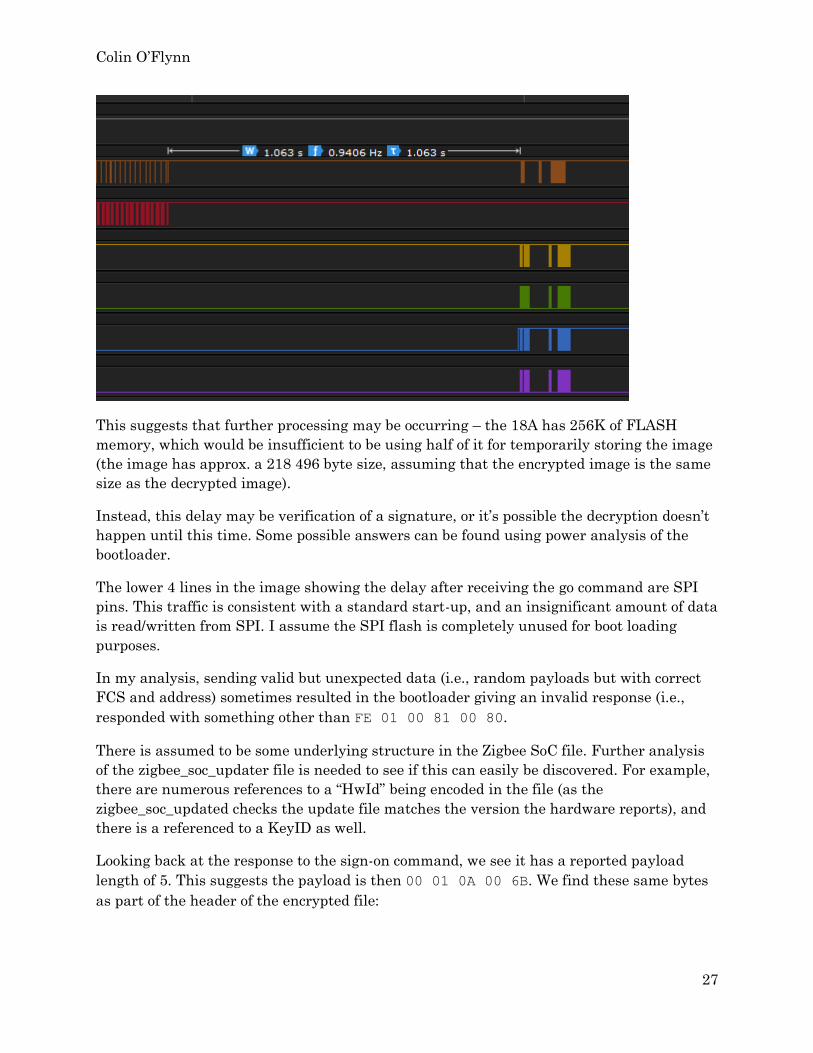
This suggests that further processing may be occurring – the 18A has 256K of FLASH
memory, which would be insufficient to be using half of it for temporarily storing the image
(the image has approx. a 218 496 byte size, assuming that the encrypted image is the same
size as the decrypted image).
Instead, this delay may be verification of a signature, or it’s possible the decryption doesn’t
happen until this time. Some possible answers can be found using power analysis of the
bootloader.
The lower 4 lines in the image showing the delay after receiving the go command are SPI
pins. This traffic is consistent with a standard start-up, and an insignificant amount of data
is read/written from SPI. I assume the SPI flash is completely unused for boot loading
purposes.
In my analysis, sending valid but unexpected data (i.e., random payloads but with correct
FCS and address) sometimes resulted in the bootloader giving an invalid response (i.e.,
responded with something other than FE 01 00 81 00 80.
There is assumed to be some underlying structure in the Zigbee SoC file. Further analysis
of the zigbee_soc_updater file is needed to see if this can easily be discovered. For example,
there are numerous references to a “HwId” being encoded in the file (as the
zigbee_soc_updated checks the update file matches the version the hardware reports), and
there is a referenced to a KeyID as well.
Looking back at the response to the sign-on command, we see it has a reported payload
length of 5. This suggests the payload is then 00 01 0A 00 6B. We find these same bytes
as part of the header of the encrypted file:

Colin O’Flynn
28
This suggests that the sign-on command is providing information which is matched to the
SoC firmware file. Unraveling the firmware update file is useful to determine where exactly
the encryption is happening, as it then allows us to inject more useful packets (which forms
the basis of an attack such as at http://wiki.newae.com/Tutorial_A5_Breaking_AES-
256_Bootloader ).
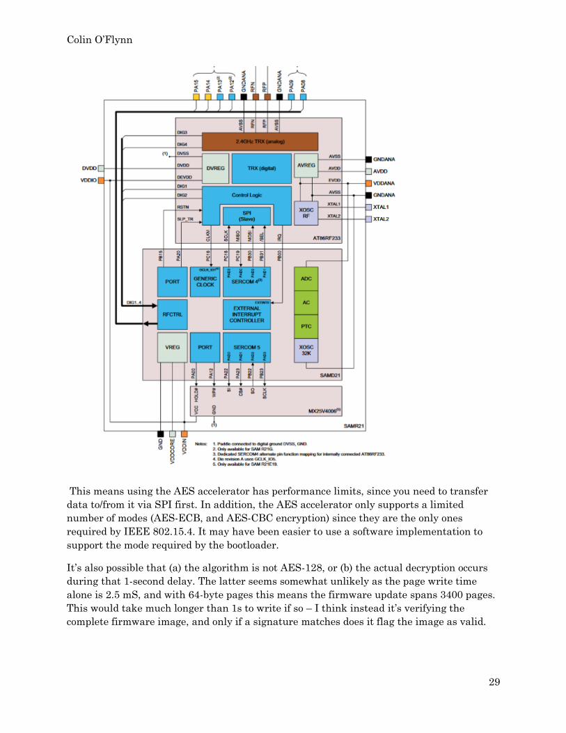
The AES accelerator on the SAMR21E18A is much simpler, and in fact the AES hardware
accelerator (which is part of the AT86RF233) I suspect to be breakable, since it’s likely the
same peripheral used in the ATMega128RFA1 (which can be attacked, as I showed at
https://eprint.iacr.org/2015/529.pdf ). This means that side-channel power analysis on the
SAMR21E18A may be more successful than on the CC2530.
These measurements were taken from the VDDCORE power supply, by inserting a resistor
in-line with the VDDCORE pin and adding an external ~1.95V power supply. This power
supply is designed to cause the internal 1.8V regulator to shut down, as it reduces the noise
on the measurement using an external supply.
Of interest I also took measurements of the VDD power supply, which is internally used by
the RF233 core which has the AES peripheral. There appeared to be no unique power
signatures beyond some spikes due to USART traffic. This would suggest that either (a)
software encryption is being used, or (b) the power signature is much different than
expected.
The setup of the SAMR21E18A is slightly odd, that makes a software implementation more
likely, even though it contains an AES hardware accelerator. The SAMR21E18A chip
internally has a separate microcontroller + an AR86RF233 die connected via SPI:
Colin O’Flynn
29
This means using the AES accelerator has performance limits, since you need to transfer
data to/from it via SPI first. In addition, the AES accelerator only supports a limited
number of modes (AES-ECB, and AES-CBC encryption) since they are the only ones
required by IEEE 802.15.4. It may have been easier to use a software implementation to
support the mode required by the bootloader.
It’s also possible that (a) the algorithm is not AES-128, or (b) the actual decryption occurs
during that 1-second delay. The latter seems somewhat unlikely as the page write time
alone is 2.5 mS, and with 64-byte pages this means the firmware update spans 3400 pages.
This would take much longer than 1s to write if so – I think instead it’s verifying the
complete firmware image, and only if a signature matches does it flag the image as valid.
Colin O’Flynn
30
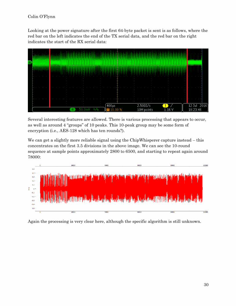
Looking at the power signature after the first 64-byte packet is sent is as follows, where the
red bar on the left indicates the end of the TX serial data, and the red bar on the right
indicates the start of the RX serial data:
Several interesting features are allowed. There is various processing that appears to occur,
as well as around 4 “groups” of 10 peaks. This 10-peak group may be some form of
encryption (i.e., AES-128 which has ten rounds?).
We can get a slightly more reliable signal using the ChipWhisperer capture instead – this
concentrates on the first 3.5 divisions in the above image. We can see the 10-round
sequence at sample points approximately 2800 to 6500, and starting to repeat again around
78000:
Again the processing is very clear here, although the specific algorithm is still unknown.
Colin O’Flynn
31
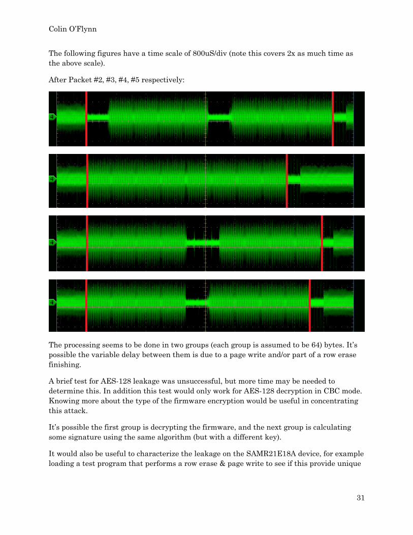
The following figures have a time scale of 800uS/div (note this covers 2x as much time as
the above scale).
After Packet #2, #3, #4, #5 respectively:
The processing seems to be done in two groups (each group is assumed to be 64) bytes. It’s
possible the variable delay between them is due to a page write and/or part of a row erase
finishing.
A brief test for AES-128 leakage was unsuccessful, but more time may be needed to
determine this. In addition this test would only work for AES-128 decryption in CBC mode.
Knowing more about the type of the firmware encryption would be useful in concentrating
this attack.
It’s possible the first group is decrypting the firmware, and the next group is calculating
some signature using the same algorithm (but with a different key).
It would also be useful to characterize the leakage on the SAMR21E18A device, for example
loading a test program that performs a row erase & page write to see if this provide unique

Colin O’Flynn
32
signatures. If these could be matched to the above images, it would give a better idea about
the bootloader process.
But it can be seen that a suitable power signature can be recorded from the bootloader on
the SAMR21E18A device. More work is required to determine what protection against
power analysis might be built into this bootloader.
For these examples, a generic target board was used which had the main bridge board
mounted onto it:
The CLK-IN point shown earlier was driven via a 1K resistor. This resistor caused the
crystal on the board to become phase-locked with an external clock. If performing clock
glitching, the crystal on the board would be removed and the clock input would be driven
with a stronger source.
For testing the above waveforms with expected programs on a SAMR21E18A, an Atmel
SAMR21 Xplained Pro board was used, which was instrumented in a similar fashion to
allow measurements on the VDDCORE supply:
Colin O’Flynn
33
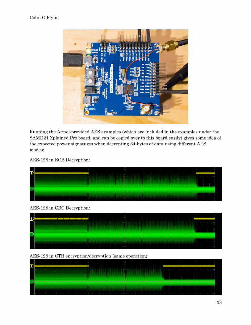
Running the Atmel-provided AES examples (which are included in the examples under the
SAMD21 Xplained Pro board, and can be copied over to this board easily) gives some idea of
the expected power signatures when decrypting 64-bytes of data using different AES
modes:
AES-128 in ECB Decryption:
AES-128 in CBC Decryption:
AES-128 in CTR encryption/decryption (same operation):

Colin O’Flynn
34
Visual inspection reveals a very close match to the observed waveforms, in particular for
the AES-CTR mode. Using AES-CTR mode is another good security practice that
complicates a basic side-channel analysis attack.
Performing an attack against AES-CTR mode requires some additional work (detailed in
https://www.iacr.org/archive/ches2007/47270001/47270001.pdf) but still remains possible,
and as can be seen here further work may reveal the keying material used for the ZigBee
SoC firmware update.
6 COLOR BR30 BULBS
The color BR30 bulbs are an older design, and of particular interest as they are the only
ones as of this whitepaper that have an over-the-air (OTA) firmware update. This means it
is possible to learn a little about the bootloading process here. A photo of the light (being
cut open) is shown below:
Inside this device, there is a CC2530 (same as on the Bridge V1.0) as shown below:
Colin O’Flynn
35
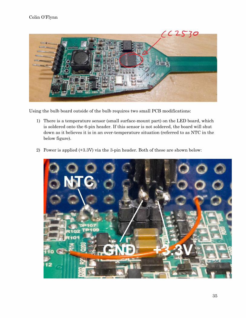
Using the bulb board outside of the bulb requires two small PCB modifications:
1) There is a temperature sensor (small surface-mount part) on the LED board, which
is soldered onto the 6-pin header. If this sensor is not soldered, the board will shut
down as it believes it is in an over-temperature situation (referred to as NTC in the
below figure).
2) Power is applied (+3.3V) via the 3-pin header. Both of these are shown below:
Colin O’Flynn
36
There is again a serial port accessible at TP114. This allows monitoring of messages from
the CC2530 device, and uses the same basic protocol as previously discussed.
FIRMWARE UPDATE INFORMATION
The firmware updates are downloaded Over The Air (OTA). The firmware file itself can be
downloaded from a fixed URL, and contains an encrypted firmware file (similar to the
firmware update for the CC2530 device).
The firmware update has the filename ConnectedLamp-Target_0012_13452_8D.sbl-ota.
This data is transmitted over the air, and written into the SPI flash on the BR30 bulb.
On start-up, the CC2530 checks this SPI flash. It appears that byte at address 0x0004 acts as a flag – if
programmed to value 0xFF it causes the device to bootload. This is useful as it can be used in trying to
load new firmware files without needing to perform an OTA update (which takes a fair amount of time
to download the new file).
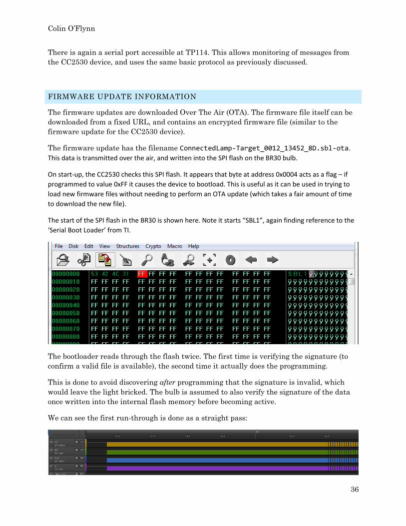
The start of the SPI flash in the BR30 is shown here. Note it starts “SBL1”, again finding reference to the
‘Serial Boot Loader’ from TI.
The bootloader reads through the flash twice. The first time is verifying the signature (to
confirm a valid file is available), the second time it actually does the programming.
This is done to avoid discovering after programming that the signature is invalid, which
would leave the light bricked. The bulb is assumed to also verify the signature of the data
once written into the internal flash memory before becoming active.
We can see the first run-through is done as a straight pass:

Colin O’Flynn
37
Notice the second pass (starting around 62s) has some “gaps.” These gaps are highlighted
here:
These gaps are the page erase being performed. This is how we know the actual write is
occurring at this time. Zooming in within one block, we see that 16 bytes are read from the
SPI flash at a time:
This would again suggest that perhaps AES-128 is being used to encrypt the firmware file.
This would agree with the existence of an AES-128 hardware module inside the CC2530.
We can use the previous “erase flash but read SRAM” bug to dig a little more. To do this, we
need a more fine-grained control of the erase process. To start with, we consider what is in
the SPI flash, as shown here:
The “2A”… is the actual OTA firmware file, the same as downloaded from the URL.
SIDE-TRACK: BRIDGE 1.0 SERIAL PORT
In addition we can look back to the Bridge 1.0 serial port, and see where the encrypted
firmware file is sent over the serial port to the Zigbee SoC.
The following is part of the log of data sent from the STM32 to the Zigbee SoC:
Colin O’Flynn
38
[Zcl,S,S=0x0004.11,768,0071000100004002400300040007000800,64]
[Zcl,S,S=0x0004.11,25,1902059700000000000000009001,64]
[Zcl,S,S=0x0004.11,25,190305000b1000018c340042000000002b1ef1ee0b000138
0000000b1000018c340042020000000000000000000000000000000000000000000000
00,64]
[Zcl,S,S=0x0004.11,25,190405000b1000018c3400422b0000002b00000000000000
0000b8ef03002a00010000665214100217303903ef402e370b25ecc04765cbe11e0e74
f7,64]
[Zcl,S,S=0x0002.11,6,0072000000,64]
[Zcl,S,S=0x0004.11,25,190505000b1000018c340042560000002ba114ee6b58b52f
f30d83681267714c7a75204d08e0749554ceab23722b80ab4646cd77cfac2e8c589e75
8c,64]
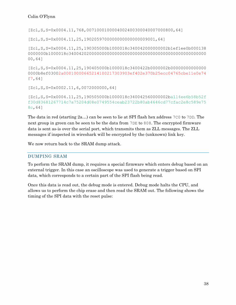
The data in red (starting 2a…) can be seen to lie at SPI flash hex address 7C0 to 7DD. The
next group in green can be seen to be the data from 7DE to 808. The encrypted firmware
data is sent as-is over the serial port, which transmits them as ZLL messages. The ZLL
messages if inspected in wireshark will be encrypted by the (unknown) link key.
We now return back to the SRAM dump attack.
DUMPING SRAM
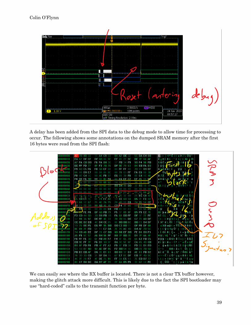
To perform the SRAM dump, it requires a special firmware which enters debug based on an
external trigger. In this case an oscilloscope was used to generate a trigger based on SPI
data, which corresponds to a certain part of the SPI flash being read.
Once this data is read out, the debug mode is entered. Debug mode halts the CPU, and
allows us to perform the chip erase and then read the SRAM out. The following shows the
timing of the SPI data with the reset pulse:
Colin O’Flynn
39
A delay has been added from the SPI data to the debug mode to allow time for processing to
occur. The following shows some annotations on the dumped SRAM memory after the first
16 bytes were read from the SPI flash:
We can easily see where the RX buffer is located. There is not a clear TX buffer however,
making the glitch attack more difficult. This is likely due to the fact the SPI bootloader may
use “hard-coded” calls to the transmit function per byte.

Colin O’Flynn
40
Performing this attack erases the bulb, making it useless. Thus it’s desired to avoid
performing this attack often due to the cost of the BR30 bulbs.
A write/erase second attack should be performed during the “decryption” phase of the
algorithm. While the SRAM dump above has clear information of interest, we may find
more by looking at a SRAM dump during the decryption phase and not the signature
verification phase.
At this stage I’ve run out of working BR30 bulbs, and due to the relatively high cost of them
decided to look into other areas.
7 LOW-COST WHITE BULBS
The newer white bulbs are available at very low cost ($15 CAD!). They make an interesting
development platform due to the very low cost.
The low-cost white bulbs are shown here:
The top part can be taken off by cutting around the seal:

Colin O’Flynn
41
The bulb being taken apart is shown in the following photos:

Colin O’Flynn
42
Removing the top heatsink requires careful scrapping of the silicon sealant, along with
removing the very tight fit of the top metal plate. Unfortunately, the test points cannot be
easily accessed without removing this plate.
Further taking apart the device by stripping the outside case shows a potting compound of
some sort:
The core processor is an Atmel ATMega2564RFR2. The test points present allow JTAG
programming of this device (detailed later).
The bulb can again be powered up using an external 3.3V supply. There is both a TX and
RX available – this uses the same sort of format as the rest of the serial ports within the
Hue system(s). The RX is pin TP112, and TX is TP111.

Colin O’Flynn
43
Looking at the strings printed on start-up, we can see the lock bits are set correctly. The
following shows the start-up message printed over the serial port (my emphasis added):
[Log,Info,ConnectedLamp,MCUCR=0x00,LockBits=0xFC,LowFuse=0xF6,HighFuse
=0x9A,ExtFuse=0xFE]
[Log,Info,ConnectedLamp,devsig=0x1EA803]
[Log,Info,S_DeviceInfo,Booting into normal mode...]
[Log,Info,S_DeviceInfo,DeviceId: Bulb_A19_DimmableWhite_v2]
[Log,Info,N_Security,LIB4.5.75]
[Log,Info,N_Security,KeyBitMask,0x0012]
[Log,Info,ConnectedLamp,Platform version 0.41.0.1,package_ZigBee
117,package_BC_Stack 104,svn 26632]
[Log,Info,ConnectedLamp,Product version WhiteLamp-Atmel
5.38.1.15095,built by LouvreZLL]
[Log,Info,A_Commissioning,Factory New at Ch: 11]
[TH,Ready,0]
We can send other messages over the serial port. For example to get the software version
we can send the GetSwVersion command (which was found by looking at strings in the
ipbridge binary):
[TH,GetSwVersion]
[TH,GetSwVersion,0,WhiteLamp-Atmel-Target,0x0012,5.38.1.15095]
Colin O’Flynn
44
Messages must be followed with a ‘\r’, the serial port can be changed to use this setting
normally. Sending a newline alone or newline+carriage return (‘\n\r’) will result in an
error.
The availability of an active serial port is potentially of great interest – this could give rise
to being susceptible to glitch attacks, or potential buffer overflows.
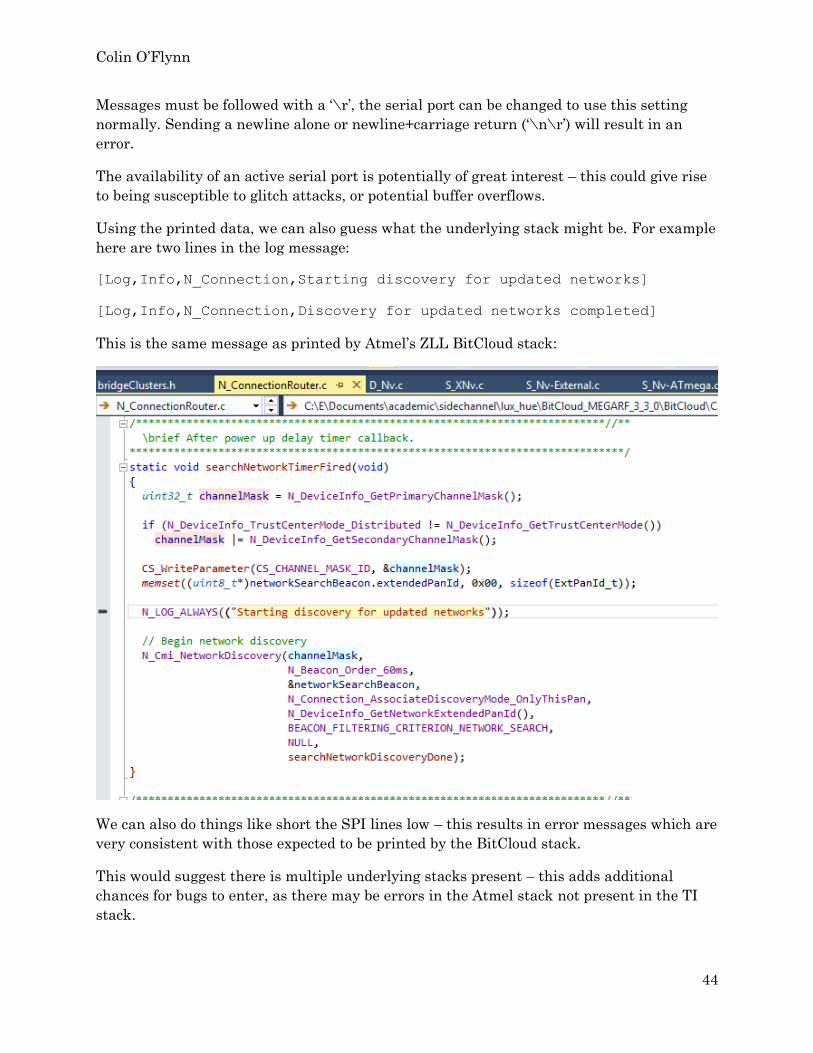
Using the printed data, we can also guess what the underlying stack might be. For example
here are two lines in the log message:
[Log,Info,N_Connection,Starting discovery for updated networks]
[Log,Info,N_Connection,Discovery for updated networks completed]
This is the same message as printed by Atmel’s ZLL BitCloud stack:
We can also do things like short the SPI lines low – this results in error messages which are
very consistent with those expected to be printed by the BitCloud stack.
This would suggest there is multiple underlying stacks present – this adds additional
chances for bugs to enter, as there may be errors in the Atmel stack not present in the TI
stack.

Colin O’Flynn
45
Also, knowing the stack allows us to understand the external SPI flash memory. For
example looking at the source code we expect the string “S_XNv2” as described in the
comments:
A dump of the SPI flash shows this exact string being present:
The SPI flash, however, seems to contain only information on the ZigBee network
configuration, and nothing of great interest such as keys or firmware.
Until an OTA update is released for the Atmel-based bulbs, it’s hard to know exactly how
the update process works. I assume it’s similar to the CC2530 device (copies data to SPI
flash, then bootloads from SPI flash).
TEST POINT CONNECTIONS
The test points on this board allow reprogramming of the ATMega2564RFR2 using a JTAG
programmer. The location of test points is as such:
TP104 = 3.3V IN
TP105 = GND
TP100 = RSTN
Colin O’Flynn
46
TP109 = TCK
TP110 = TMS
TP113 = TDO
TP114 = TDI
While soldering wires to these test-points requires removal of the LED board / heat-sink
assembly, it should be possible to design a small PCB-jig that can press against these test
points, and is inserted from the top without removing the LED board / heat-sink assembly.
This would make it possible to re-use the low-cost white Hue LEDs as a generic
development platform for those doing wireless sensor network (WSN) research.
FUSE INFORMATION
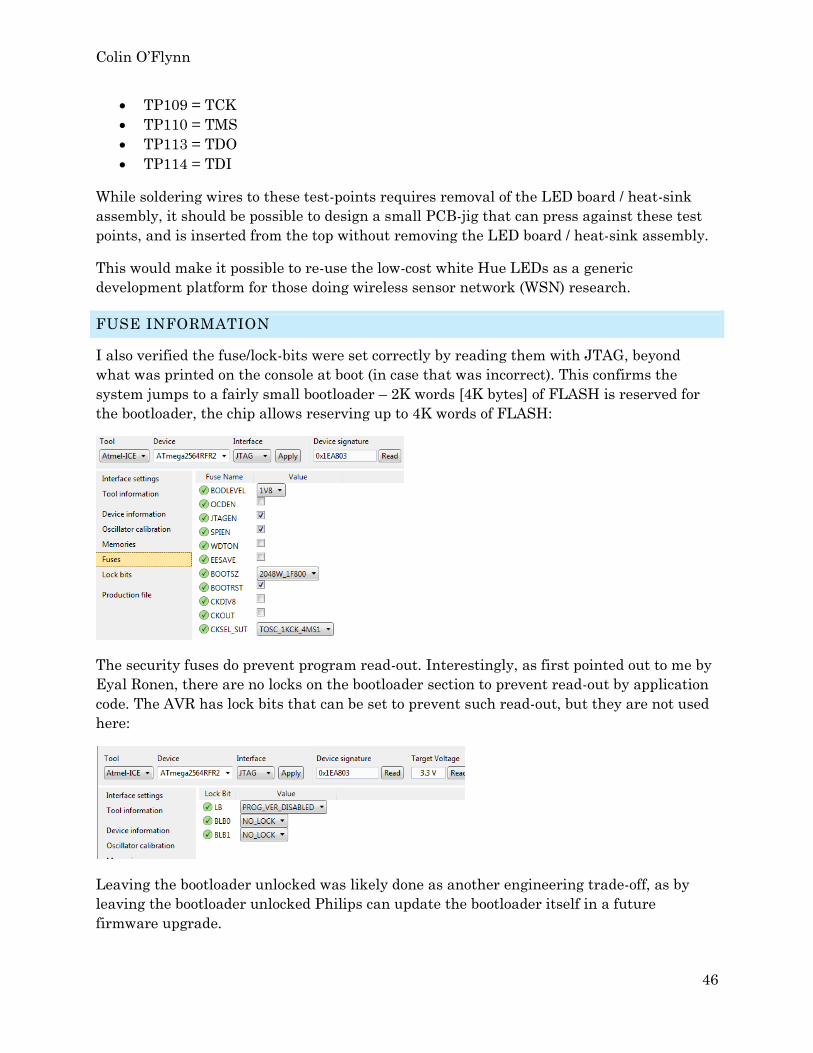
I also verified the fuse/lock-bits were set correctly by reading them with JTAG, beyond
what was printed on the console at boot (in case that was incorrect). This confirms the
system jumps to a fairly small bootloader – 2K words [4K bytes] of FLASH is reserved for
the bootloader, the chip allows reserving up to 4K words of FLASH:
The security fuses do prevent program read-out. Interestingly, as first pointed out to me by
Eyal Ronen, there are no locks on the bootloader section to prevent read-out by application
code. The AVR has lock bits that can be set to prevent such read-out, but they are not used
here:
Leaving the bootloader unlocked was likely done as another engineering trade-off, as by
leaving the bootloader unlocked Philips can update the bootloader itself in a future
firmware upgrade.

Colin O’Flynn
47
The disadvantage from a security perspective is that if an alternate method of loading code
is found (for example – the bootloader has a flag to allow unencrypted binaries to be loaded,
etc.), we could then load a program to read the bootloader out and determine the secret
encryption keys.
Note the AVR’s architecture prevents a basic glitch attack from working to read the
bootloader section out. As the AVR is a Harvard architecture, the data and code memory is
separate. Loading data from code memory requires special instructions, thus glitching some
arbitrary transmit loop cannot result in code memory dumps.
8 CONCLUSIONS
A lightbulb worm doesn’t exist today, but the “makings” of such a worm seem to exist in the
architecture of any smart-lighting system. These systems involved wireless connections,
where the very simple devices have limited ability to know what network they should join.
An attacker can thus find ways to cause devices to switch networks, and if the device can be
reflashed once under their control, a worm is trivial to generate from this arrangement.
The specific ZigBee Light Link (ZLL) implementation in Philips Hue takes a number of
precautions to reduce the risk of this happening – using encrypted firmware updates for
example to stop arbitrary code from being flashed, and using unique root passwords to
hopefully stop someone from logging into the Bridge devices en-masse to attack the network
from the Ethernet side.
Some engineering trade-offs were made that have the potential to cause serious problems.
It appears all bulbs of the same type use the same encryption key for the firmware image,
and if that key leaks it may be difficult to securely change the key. Realistically, such trade-
offs are simply part of any product design and it’s difficult to call them “good” or bad”
design.
This paper has outlined various methods that might be used in further analysis of the
system. Examples of glitch attacks to dump SRAM, alongside power analysis to determine
where data processing occurred within the bootloader was demonstrated. Finally, an
example of how to get a root console on the newer Bridge 2.0 devices was presented, which
will be useful in performing further analysis of the binaries on these devices.
Readers interested in learning more about what sort of leakage can happen with a lightbulb
attack, and then looking at how they can be applied, are encouraged to see Eyal Ronen’s
current and future publications (http://www.wisdom.weizmann.ac.il/~eyalro/).
Colin O’Flynn
48
ABOUT THE AUTHOR
Colin O'Flynn has developed the world's first open-source platform for side-channel power
analysis and glitching attacks, and has spoken around the world about the application of
this platform to various targets. You can read more about this platform (called
ChipWhisperer), including seeing examples of how to perform these attacks at
http://www.chipwhisperer.com .
Colin is currently finishing a PhD, and alongside that started NewAE Technology Inc. to
sell the open-source hardware that resulted from the ChipWhisperer project, and also offers
training and consulting services through this company. See www.newae.com for more
information.
Before working in embedded security, he developed solutions for low-power wireless
embedded systems, and continues some embedded design work as part of NewAE, as well
as writing about FPGA design for Circuit Cellar magazine. He lives in Halifax, NS, Canada.
He maintains a blog at www.oflynn.com, which contains various ongoing electronics
projects (and some security work too).