
Design, synthesis and applications of novel soluble n ...
175
This document is downloaded from DR‑NTU (https://dr.ntu.edu.sg) Nanyang Technological University, Singapore. Design, synthesis and applications of novel soluble n‑heteroacenes Wang, Chengyuan 2015 Wang, C. (2015). Design, synthesis and applications of novel soluble n‑heteroacenes. Doctoral thesis, Nanyang Technological University, Singapore. https://hdl.handle.net/10356/65472 https://doi.org/10.32657/10356/65472 Downloaded on 20 Mar 2022 11:44:02 SGT
Transcript of Design, synthesis and applications of novel soluble n ...

This document is downloaded from DR‑NTU (https://dr.ntu.edu.sg)Nanyang Technological University, Singapore.
Design, synthesis and applications of novelsoluble n‑heteroacenes
Wang, Chengyuan
2015
Wang, C. (2015). Design, synthesis and applications of novel soluble n‑heteroacenes.Doctoral thesis, Nanyang Technological University, Singapore.
https://hdl.handle.net/10356/65472
https://doi.org/10.32657/10356/65472
Downloaded on 20 Mar 2022 11:44:02 SGT

DESIGN, SYNTHESIS AND APPLICATIONS OF NOVEL SOLUBLE N-HETEROACENES
CHENGYUAN WANG
SCHOOL OF MATERIALS SCIENCE AND ENGINEERING
2015

Design, Synthesis and Applications of Novel Soluble N-
heteroacenes
School of Materials Science and Engineering
A thesis submitted to the Nanyang Technological University in partial fulfilment of the requirement for the
degree of Doctor of Philosophy
2015

Acknowledgements
Acknowledgements
The author would like to acknowledge the scholarship from NTU for financial support.
The author would like to take this opportunity to express gratefulness to his supervisor,
Assoc. Prof. Qichun Zhang, for his invaluable guidance and selflessly share of knowledge
and experience.
The author would like to thank Assoc. Prof. Pooi See Lee, Assoc. Prof. Yang Zhao, Asst.
Prof. Fengwei Huo, Asst. Prof. Yanli Zhao for their kind support.
The author would like to express special acknowledgements to Prof. Hiroko Yamada, Assoc.
Prof. Naoki Aratani in Nara Institute of Science & Technology (NAIST) for their valuable
guidance and discussion.
The author would like to thank Dr. Jing Zhang, Dr. Benlin Hu, Mr. Takuya Okabe (NAIST)
for their kind assistance in devices fabrication.
The author would like to thank Dr. Peiyang Gu, Dr. Gang Li, Dr. Weiwei Xiong, Dr.
Guankui Long, Dr. Junkuo Gao, Dr. Kaiqi Ye, Dr. Jiansheng Wu, Dr. Yi Zhou, Dr. Jun Zhao,
Dr. Guodong Zhang, Dr. Liang Xu, Dr. Cui-e Zhao, Mr. Wangqiao Chen, Mrs. Lina Nie, Mr.
Zilong Wang, Mr. Bin Gu and other group members for their valuable help and discussion.
He also would like to thank Dr. Jin Wu, Mr. Jiangxin Wang, Mr. Masataka Yamashita
(NAIST) for their support. He would like to acknowledge all the friends and colleagues who
have helped in any way during his Ph. D. candidate.
Finally, the author would like to thank his family for their continuous support and
encouragement in his graduate study.

Table of Contents
Table of Contents
Abstract ...................................................................................................................................... i
Figure Captions ........................................................................................................................ iii
Scheme Captions ...................................................................................................................... ix
Table Captions .......................................................................................................................... x
Abbreviations ........................................................................................................................... xi
Chapter 1 ................................................................................................................................... 1
Introduction ............................................................................................................................... 1
1.1 Background & Motivation ......................................................................................... 1
1.1.1 Charming Properties of N-heteroacenes ................................................................... 1
1.1.2 Applications of N-heteroacenes ................................................................................ 4
1.2 Hypothesis ..................................................................................................................... 11
1.3 Objectives ...................................................................................................................... 13
1.4 Scope ............................................................................................................................. 15
1.5 References ..................................................................................................................... 16
Chapter 2 ................................................................................................................................. 20

Table of Contents
N-heteroacenes for Organic Memories ................................................................................... 20
2.1 Literature Review .......................................................................................................... 20
2.2 D-A Molecules with Different N-heteroacene Units as Acceptor Moiety .................... 24
2.2.1 Molecular Design ................................................................................................... 24
2.2.2 Synthesis of TPA-BIP ............................................................................................ 25
2.2.3 Molecular Characterization .................................................................................... 27
2.2.4 Memory Device Fabrication Based on TPA-BIP .................................................. 33
2.2.5 Memory Characteristics of TPA-BIP .................................................................... 35
2.2.6 Mechanism Discussion ........................................................................................... 37
2.2.7 Summary ................................................................................................................. 39
2.3 D-A Molecules with Multiple Acceptor Moieties ......................................................... 40
2.3.1 Molecular Design ................................................................................................... 40
2.3.2 Synthesis of TPA-2BIP & TPA-3BIP .................................................................. 40
2.3.3 Molecular Characterization .................................................................................... 42
2.3.4 Memory Device Fabrication Based on TPA-2BIP & TPA-3BIP ......................... 50
2.3.5 Memory Characteristics of TPA-2BIP & TPA-3BIP ........................................... 52
2.3.6 Mechanism Discussion ........................................................................................... 54

Table of Contents
2.3.7 Summary ................................................................................................................. 57
2.4 D-A Molecules with Strong Electron-deficient N-heteroacene and Multiple Donors .. 57
2.4.1 Molecular Design ................................................................................................... 57
2.4.2 Synthesis of 2TPA-BTTT ...................................................................................... 58
2.4.3 Molecular Characterization .................................................................................... 59
2.4.4 Memory Device Fabrication Based on 2TPA-BTTT ............................................ 69
2.4.5 Memory Characteristics of 2TPA-BTTT .............................................................. 70
2.4.6 Mechanism Discussion ........................................................................................... 72
2.4.7 Summary ................................................................................................................. 74
2.5 References ..................................................................................................................... 74
Chapter 3 ................................................................................................................................. 79
N-heteroacenes for Organic Photovoltaics .............................................................................. 79
3.1 Literature Review .......................................................................................................... 79
3.2 D-π-A Small Molecule with N-heteroacene as Acceptor .............................................. 83
3.2.1 Molecular Design ................................................................................................... 83
3.2.2 Synthesis of BDT-3DTT-BIP ................................................................................ 84
3.2.3 Molecular Characterization .................................................................................... 86

Table of Contents
3.2.4 OPV Device Fabrication Based on BDT-3DTT-BIP ............................................ 95
3.2.5 OPV Characteristics of BDT-3DTT-BIP .............................................................. 96
3.2.6 Results Discussion ................................................................................................ 102
3.2.7 Summary ............................................................................................................... 106
3.3 References ................................................................................................................... 107
Chapter 4 ............................................................................................................................... 112
N-heteroacenes for Organic Field-effect Transistors ............................................................ 112
4.1 Literature Review ........................................................................................................ 112
4.2 Large N-heteroacenes for Air-stable n-type OFETs ................................................... 120
4.2.1 Molecular Design ................................................................................................. 120
4.2.2 Synthesis of OANQ .............................................................................................. 121
4.2.3 Molecular Characterization .................................................................................. 122
4.2.4 OFET Device Fabrication Based on OANQ ........................................................ 132
4.2.5 OFET Characteristics of OANQ .......................................................................... 135
4.2.6 Results Discussion ................................................................................................ 136
4.2.7 Summary ............................................................................................................... 140
4.3 References ................................................................................................................... 140

Table of Contents
Chapter 5 ............................................................................................................................... 145
Conclusions & Future Work ................................................................................................. 145
5.1 Conclusions ................................................................................................................. 145
5.2 Future Work of N-heteroacenes for Organic Memories .............................................. 147
5.3 Future Work of N-heteroacens for Organic Photovoltaics .......................................... 148
5.4 Future Work of N-heteoacenes for Organic Field-effect Transistors .......................... 149
Appendixes ........................................................................................................................... 151
Publications during Ph. D. Candidate ................................................................................... 151
Abstract
i
Abstract
N-heteroacenes with the CH groups in the backbone of acenes replaced by N atoms are
expected to own charming semiconducting properties and potential practical applications in
organic electronics. The electron-deficient N-heteroacenes can be used as acceptor moieties
in D-A molecules or n-type semiconductors depending on the application requirements.
Although the researchers in all over the world are devoted to developing commercially
available organic electronics, the study of organic memories, photovoltaics (OPVs) and field-
effect transistors (OFETs) can still not stride out laboratory conditions, and the ultimate
organic materials, which can satisfy all requirements for practical applications in the three
types of devices are in high desire. Inspired by this gap, this dissertation focuses on design
and synthesis of novel soluble N-heteroacenes and investigation of their applications in
organic memories, OPVs and OFETs. For organic memories, the molecules have been
designed based on two assumptions about multiple electron “traps” or multiple electrons
intermolecular charge transfer, and accordingly, different electron-deficient N-heteroacene
units are combined together to induce multiple electron “traps” or strong electron-deficient
N-heteroacenes are utilized to accept multiple electrons. The memory devices have been
fabricated and the corresponding switching behaviors, the ON/OFF ratios, the endurance and
retention performance have been evaluated. Molecular calculation has been carried out to
study the structure-property relationship. In summary, an efficient molecular designing
strategy to approach rewritable, multilevel organic memory materials has been developed.
For OPVs, the D-π-A structure molecules are designed with large conjugated N-heteroacene
as acceptor moiety and linked to widely investigated donor units by π-bridges. The large
conjugation of N-heteroacenes is expected to induce broad absorption and facilitate charge

Abstract
ii
carriers’ transport. The typical BHJ architecture OPV devices have been fabricated and the
corresponding PCE, Voc, Jsc, and FF are investigated. Morphology analysis of the organic
films has been carried out to study the effect of molecular stacking on the device
performance. In summary the as-designed molecule has showed PCE up to ~2%, which is
expected to own better performance after structure modification. For OFETs, large
conjugated N-heteroacenes with deep LUMO level lower than -4.0 eV has been designed.
The single-crystal OFET devices have been fabricated and the corresponding transfer and
output curves, VTH, ON/OFF ratios and field-effect mobility are investigated. Theoretical
calculation has been conducted to study the ideal mobility of molecules and structure-
property relationship. In summary a new family of N-heteroacenes have been developed for
air-stable, high performance n-type OFETs.

Figure Captions
iii
Figure Captions
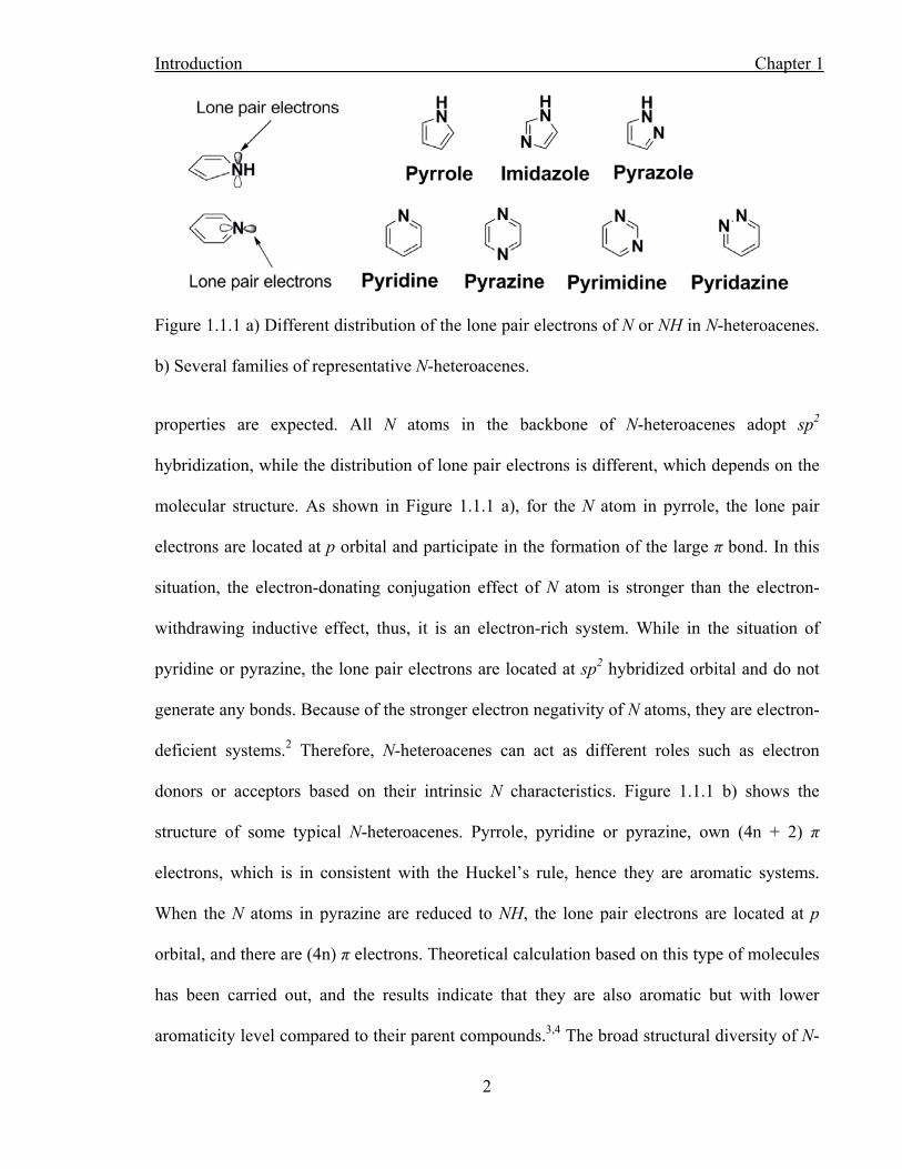
Figure 1.1.1 a) Different distribution of the lone pair electrons of N or NH in N-heteroacenes.
b) Several families of representative N-heteroacenes.
Figure 1.1.2 Representative synthetic route for N-heteroacenes.
Figure 1.1.3 a) Schematic graph of a typical ORM device. b) Data storage performance of a
ternary ORM device (reproduced based on literature).
Figure 1.1.4 a) Schematic graph of a typical BHJ architecture OPV device. b) Fundamental
steps of photocurrent generation. c) J-V characteristics of a typical OPV device. Vmp and Jmp
are voltage and current, respectively, at which the power output of a device reaches its
maximum. JL is the photocurrent (reproduced based on literature).
Figure 1.1.5 a) Bottom gate/bottom contact device. b) Bottom gate/top contact device. c) Top
gate/top contact device. d) Top gate/bottom contact device. e) Output characteristics and f)
transfer curves of a pentacene-based Bottom Gate/Top Contact OFET device (reproduced
based on literature).
Figure 2.1.1 a) Molecular structure of representative multilevel ORM polymers. b) I-V curves
for 1. c) I-V curves for 2 (reproduced based on literature).
Figure 2.1.2 Molecular structures of representative multilevel ORM small molecules.
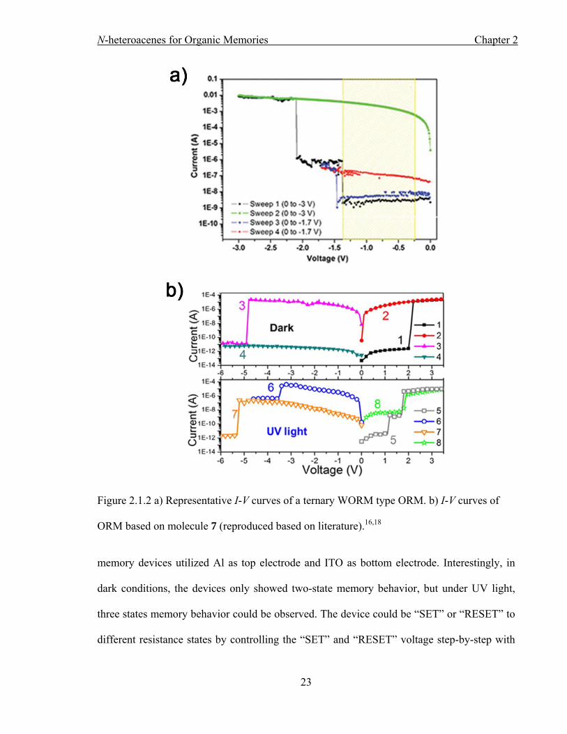
Figure 2.1.3 a) Representative I-V curves of a ternary WORM type ORM. b) I-V curves of
ORM based on molecule 7 (reproduced based on literature).

Figure Captions
iv
Figure 2.2.1.1 Molecular structure of TPA-BIP.
Figure 2.2.3.1.1 HR MS (ESI) spectra of TPA-BIP.
Figure 2.2.3.2.1 1H NMR spectra of TPA-BIP in CD2Cl2.
Figure 2.2.3.2.2 13C NMR spectra of TPA-BIP in CDCl3.
Figure 2.2.3.3.1 Images of a) top view & b) side view of TPA-BIP crystals.
Figure 2.2.3.3.2 a) Top view and b) side view of TPA-BIP crystal structure. c) Molecular
stacking of TPA-BIP.
Figure 2.2.3.4.1 Normalized UV-vis absorption spectra of TPA-BIP in CH3CN (red line) and
in film (blue line).
Figure 2.2.3.5.1 Cyclic voltammetric (CV) curves of TPA-BIP in anhydrous CH3CN.
Figure 2.2.4.1 a) AFM images of a 5 μm × 5 μm TPA-BIP film. b) Corresponding 3D AFM
images. c) XRD patterns of the corresponding film.
Figure 2.2.5.1 a) I-V curves of ITO/TPA-BIP/Pt device. b) Resistance distribution of 14
cycles. c) Retention performance of ITO/TPA-BIP/Pt device.
Figure 2.2.6.1 Electron density distribution of HOMO & LUMO levels of TPA-BIP.
Figure 2.2.6.2 Electrostatic potential (ESP) calculation of TPA-BIP in HRs & LRs.
Figure 2.3.3.1.1 HR MS (ESI) spectra of TPA-2BIP.
Figure 2.3.3.1.2 HR MS (MOLDI-TOF) spectra of TPA-3BIP.

Figure Captions
v
Figure 2.3.3.2.1 1H NMR spectra of TPA-2BIP in CDCl3.
Figure 2.3.3.2.2 13C NMR spectra of TPA-2BIP in CDCl3.
Figure 2.3.3.2.3 1H NMR spectra of TPA-3BIP in CDCl3.
Figure 2.3.3.2.4 13C NMR spectra of TPA-3BIP in CDCl3.
Figure 2.3.3.3.1 Normalized UV-vis absorption spectra of a) TPA-2BIP (red line: in solution,
blue line: in film) & b) TPA-3BIP (red line: in solution, blue line: in film).
Figure 2.3.3.4.1 Cyclic voltammetric (CV) curves of a) TPA-2BIP & b) TPA-3BIP in
anhydrous CH2Cl2.
Figure 2.3.4.1 a) & c) AFM images of 5 μm × 5 μm the films of TPA-2BIP & TPA-3BIP,
respectively. b) & d) 3D AFM images of the corresponding films, respectively. e) & f) XRD
patterns of the films of TPA-2BIP & TPA-3BIP, respectively.
Figure 2.3.5.1 a) & b) I-V curves, c) & d) resistance distribution, e) & f) retention
performance of the ITO/TPA-2BIP (or TPA-3BIP)/Au devices, respectively.
Figure 2.3.6.1 Electron density distribution of a) TPA-2BIP & b) TPA-3BIP.
Figure 2.4.3.1.1 HR MS (ESI) spectra of 17.
Figure 2.4.3.1.2 HR MS (ESI) spectra of 2TPA-BTTT.
Figure 2.4.3.2.1 1H NMR spectra of 17 in CDCl3.
Figure 2.4.3.2.2 13C NMR spectra of 17 in CDCl3.

Figure Captions
vi
Figure 2.4.3.2.3 1H NMR spectra of 2TPA-BTTT in CD2Cl2.
Figure 2.4.3.2.4 13C NMR spectra of 2TPA-BTTT in CD2Cl2.
Figure 2.4.3.3.1 a) Top view & b) side view of the crystal structure of 2TPA-BTTT. c)
Molecular stacking of 2TPA-BTTT.
Figure 2.4.3.4.1 Normalized UV-vis absorption spectra of 2TPA-BTTT (magenta line: in
solution, violet line: in film).
Figure 2.4.3.5.1 Cyclic voltammetric (CV) curves of 2TPA-BTTT in anhydrous CH2Cl2.
Figure 2.4.4.1 a) AFM image of a 5 μm × 5 μm film of 2TPA-BTTT. b) XRD patterns of the
corresponding film.
Figure 2.4.5.1 a) I-V curves, b) resistance distribution & c) retention performance of
ITO/2TPA-BTTT/Au device.
Figure 2.4.6.1 a) Electron density distribution of 2TPA-BTTT. b) Energy diagrams of
ITO/2TPA-BTTT/Au system. c) Proposed mechanisms for the multilevel memory behavior.
Figure 3.1.1 Molecular structure of some representative p-type small molecules.
Figure 3.2.3.1.1 HR MS (MALDI-TOF) spectra of 15.
Figure 3.2.3.1.2 HR MS (MALDI-TOF) spectra of BDT-3DTT-BIP.
Figure 3.2.3.2.1 1H NMR spectra of 13 in CDCl3.
Figure 3.2.3.2.2 1H NMR spectra of 15 in CDCl3.
Figure Captions
vii
Figure 3.2.3.2.3 13C NMR spectra of 15 in CDCl3.
Figure 3.2.3.2.4 1H NMR spectra of BDT-3DTT-BIP in CD2Cl2.
Figure 3.2.3.2.4 13C NMR spectra of BDT-3DTT-BIP in CD2Cl2.
Figure 3.2.3.3.1 Normalized UV-vis absorption spectra of BDT-3DTT-BIP film (magenta),
BDT-3DTT-BIP/PC61BM blended film (navy) & BDT-3DTT-BIP/PC71BM blended film
(violet).
Figure 3.2.5.1 a) J-V curves and b) EQE plots of the ITO/PEDOT:PSS/BDT-3DTT-
BIP:PC61BM/Ca/Al device (square), ITO/PEDOT:PSS/BDT-3DTT-BIP:PC71BM /Ca/Al
device (triangle), and ITO/MoO3/BDT-3DTT-BIP:PC71BM/Ca/Al device (sphere).
Figure 3.2.6.1.1 Electron density distribution of HOMO & LUMO levels of BDT-3DTT-BIP.
Figure 3.2.6.2.1 AFM images of a) BDT-3DTT-BIP/PC61BM blended film without DIO, b)
BDT-3DTT-BIP/PC61BM blended film with DIO, c) BDT-3DTT-BIP/PC71BM blended
film with DIO, d) BDT-3DTT-BIP/PC71BM blended film with DIO and MoO3 buffer layer.
Figure 3.2.6.3.1 XRD patterns of corresponding films (magenta: BDT-3DTT-BIP/PC61BM
blended film without DIO, navy: BDT-3DTT-BIP/PC61BM blended film with DIO, orange:
BDT-3DTT-BIP/PC71BM blended film with DIO on PEDOT:PSS, violet: BDT-3DTT-
BIP/PC71BM blended film with DIO on MoO3).
Figure 4.1.1 Molecular structures of the representative NDIs and PDIs derivatives.
Figure 4.1.2 Molecular structures of the representative oligoacenes.

Figure Captions
viii
Figure 4.2.3.1.1 HR MS (ESI) spectra of THNQ.
Figure 4.2.3.1.2 HR MS (ESI) spectra of OANQ.
Figure 4.2.3.2.1 1H NMR spectra of THNQ in CDCl3.
Figure 4.2.3.2.2 13C NMR spectra of THNQ in CDCl3.
Figure 4.2.3.2.3 1H NMR spectra of OANQ in CDCl3.
Figure 4.2.3.2.4 13C NMR spectra of OANQ in CDCl3.
Figure 4.2.3.3.1 a) & d) Top view, b) & e) side view, c) & f) molecular stacking of THNQ &
OANQ crystal structure, respectively.
Figure 4.2.3.4.1 Normalized UV-vis absorption spectra of THNQ & OANQ in CH2Cl2.
Figure 4.2.3.5.1 Cyclic voltammetric (CV) curves of THNQ & OANQ in anhydrous CH2Cl2.
Figure 4.2.4.1 Representative photos of a) micrometer-sized crystal sheets & b) single-crystal
OFET device.
Figure 4.2.4.2 a) TEM, b) SEAD & c) XRD patterns of OANQ micrometer-sized crystal
sheets.
Figure 4.2.5.1 a) Transfer & b) output curves of typical single-crystal OFET device.
Figure 4.2.6.1 Electron density distribution of HOMO and LUMO levels of THNQ &
OANQ.
Figure 4.2.6.2 Hoping routes of OANQ in the crystals.

Scheme Captions
ix
Scheme Captions
Scheme 2.2.2.1 Synthetic route for TPA-BIP.
Scheme 2.3.2.1 Synthetic route for TPA-2BIP and TPA-3BIP.
Scheme 2.4.2.1 Synthetic route for 2TPA-BTTT.
Scheme 3.2.2.1 Synthetic route for BDT-3DTT-BIP.
Scheme 4.2.2.1 Synthetic route for OANQ.
Scheme 5.2.1 Synthetic route for the typical donor units.
Scheme 5.2.2 Synthetic route for the target D-A molecules.
Scheme 5.3.1 Synthetic route for 7a–c.
Scheme 5.3.1 Synthetic route for 8.

Table Captions
x
Table Captions
Table 3.2.3.4.1 Statistic ionization potentials of BDT-3DTT-BIP.
Table 3.2.5.1 ITO/PEDOT:PSS/BDT-3DTT-BIP:PC61BM/Ca/Al device parameters with
different donor:acceptor ratios.
Table 3.2.5.2 ITO/PEDOT:PSS/BDT-3DTT-BIP:PC61BM (1:1.2)/Ca/Al device parameters
at different annealing temperature.
Table 3.2.5.3 ITO/PEDOT:PSS/BDT-3DTT-BIP:PC61BM (1:1.2)/Ca/Al device parameters
with different DIO concentration.
Table 3.2.5.4 Optimal performance parameters of the ITO/PEDOT:PSS/BDT-3DTT-
BIP:PC61BM (or PC71BM)/Ca/Al devices.
Table 4.1.1 Summarized OFET performance parameters of the representative NDIs & PDIs
derivatives. *Measured under ambient conditions.
Table 4.1.2 Summarized OFET performance parameters of the representative oligoacens.
*Measured under ambient conditions.
Table 4.2.3.5.1 Summarized energy levels for THNQ and OANQ. [a]Energy levels determined
from experimental results. [b]Energy levels deduced from DFT calculations (B3LYP/6-31G*).
Table 4.2.6.1 The electronic couplings (V) for all the hopping pathways of OANQ.

Abbreviations
xi
Abbreviations
D-A Donor-Acceptor
OLED Organic Light-emitting Diodes
ORM Organic Resistance Memory
OPV Organic Photovoltaic
OFET Organic Field-effect Transistor
HR MS High Resolution Mass Spectroscopy
ESI Electrospray Ionization
MALDI-TOF Matrix-Assisted Laser Desorption/Ionization-Time of Flight
NMR Nuclear Magnetic Resonance Spectroscopy
XRD X-ray Diffraction
UV-vis Ultraviolet-visible
TEM Transmission Electron Microscopy
SAED Selected-Area Electron Diffraction
AFM Atomic Force Microscopy
Si Silicon
Abbreviations
xii
Al Aluminum
Ca Calcium
Pt Platinum
Au Gold
ITO Indium Tin Oxide
2D Two Dimensional
3D Three Dimensional
HOMO Highest Occupied Molecular Orbital
LUMO Lowest Unoccupied Molecular Orbital

Introduction Chapter 1
1
Chapter 1
Introduction
1.1 Background & Motivation
1.1.1 Charming Properties of N-heteroacenes
Since the discovery of conductive polymers in 1977 by Heeger, A. J. Shirakawa, H. and
MacDiarmid, A. G., the development of organic π-conjugated materials have attracted a lot
of attention, and large progress have been achieved in the exploration of their unique optical
and electrical properties.1 To date, millions of π-conjugated materials, including both
polymers and small molecules, have been developed. Organic small molecules have 1) well-
defined molecular structures, which make them be able to keep good batch to batch repeat; 2)
easily controlled energy levels, which are favor for the demonstration of structure-property
relationship; and 3) more accurate calculation-experiment matching, contributing to better
investigation of intrinsic semiconducting mechanism. Thus, developing novel π-conjugated
small molecules are crucial for both fundamental study and practical applications.
The π-conjugated materials can be classified as either a p-type (electron-rich systems, often
play as donors), in which hole charge carriers are dominant, or n-type (electron-deficient
systems, often act as acceptors), in which electron charge carriers are dominant. Acenes, a
large family of π-conjugated small molecules, have proved to be excellent p-type
semiconducting materials in organic electronics. When the CH groups in acenes’ backbone
are replaced by N atoms, or NH units, N-heteroacenes, the analogues of acenes, are generated
and the intrinsic molecular structures have been changed, and special semiconducting
Introduction Chapter 1
2
Figure 1.1.1 a) Different distribution of the lone pair electrons of N or NH in N-heteroacenes.
b) Several families of representative N-heteroacenes.
properties are expected. All N atoms in the backbone of N-heteroacenes adopt sp2
hybridization, while the distribution of lone pair electrons is different, which depends on the
molecular structure. As shown in Figure 1.1.1 a), for the N atom in pyrrole, the lone pair
electrons are located at p orbital and participate in the formation of the large π bond. In this
situation, the electron-donating conjugation effect of N atom is stronger than the electron-
withdrawing inductive effect, thus, it is an electron-rich system. While in the situation of
pyridine or pyrazine, the lone pair electrons are located at sp2 hybridized orbital and do not
generate any bonds. Because of the stronger electron negativity of N atoms, they are electron-
deficient systems.2 Therefore, N-heteroacenes can act as different roles such as electron
donors or acceptors based on their intrinsic N characteristics. Figure 1.1.1 b) shows the
structure of some typical N-heteroacenes. Pyrrole, pyridine or pyrazine, own (4n + 2) π
electrons, which is in consistent with the Huckel’s rule, hence they are aromatic systems.
When the N atoms in pyrazine are reduced to NH, the lone pair electrons are located at p
orbital, and there are (4n) π electrons. Theoretical calculation based on this type of molecules
has been carried out, and the results indicate that they are also aromatic but with lower
aromaticity level compared to their parent compounds.3,4 The broad structural diversity of N-

Introduction Chapter 1
3
heteroacenes can be achieved by varying the intrinsic characteristics, the number and position
of N atoms, besides of other common molecular modification strategies. As the structure
changed, the semiconducting properties of N-heteroacenes can be tuned accordingly. In
addition, N-heteroacenes are more stable than their counterpart acenes because they are more
resistive to oxygen. All the advantages of N-heteroacenes such as multiple applications in
building up molecules, different aromaticity, high structure diversity and good environmental
stability make them good candidates in the applications of organic electronics and promising
semiconducting performance are expected.
Figure 1.1.2 Representative synthetic route for N-heteroacenes.
Currently, most of the N-heteroacenes applied in organic electronics are linearly fused
systems. To approach them, people usually utilize conventional substitution reaction between
ortho-diamine based acenes and ortho-diketone, ortho-dihydroxy, ortho-dicyano, or ortho-
dihalogen substituted acenes. As shown in Figure 1.1.2, when ortho-diamine based acenes
react with ortho-diketone, in certain situations azaacenes can be directly obtained. However,
if the target products are highly electron-deficient, only hydro-azaacenes can be separated.
The reaction between ortho-diamine based acenes and ortho-dihydroxy, ortho-dicyano, or
ortho-dihalogen substituted acenes generally produce hydro-azaacenes. Further oxidation of

Introduction Chapter 1
4
hydro-azaacenes possibly gives their corresponding azaacenes. With these preparation
strategies, a series of N-heteroacenes from low to high conjugation, i.e. anthracene to
heptacene analogues have been successfully developed.
1.1.2 Applications of N-heteroacenes
Organic electronics have been predicted to be the next generation of electronics. Compared
with the conventional Si-based inorganic electronics, organic electronics are cheaper with
lower fabrication cost, more flexible and easier to process. In addition, there are various
materials which can be specialized for certain requirements through molecular designing
strategies. All the advantages make organic electronics popular and scientists all over the
world are devoted themselves into this area. Among all the organic electronics, organic
memories, OLEDs, OPVs and OFETs are closely connected to people’s daily life. OLEDs
have been well developed and commercialized in practical application, however, the
development for organic memories, OPVs and OFETs still stays in laboratory research. A
key factor which limits their development is that there are few of ultimate organic materials
that have potential practical application in the three types of devices. Inspired by this gap and
considering the charming advantages of N-hetroacenes, this dissertation will focus on design
and synthesis of novel soluble N-heteroacenes and the investigation of their applications in
organic memories, OPVs and OFETs.
1.1.2.1 Applications in Organic Memories
The novel organic memories should combine the advantages of the three leading memory
technologies of today, which are expected to own the non-volatile ability of flash memory,
the high switching speed of dynamic random access memory (DRAM), the high data storage

Introduction Chapter 1
5
Figure 1.1.3 a) Schematic graph of a typical ORM device. b) Data storage performance of a
ternary ORM device (reproduced based on literature).6,8
density and high cycling endurance of hard-disk drives (HDDs). ORMs are promising
candidates satisfying all the requirements.5 Figure 1.1.3 a) shows the schematic structure of a
typical ORM device, which has a simple metal-insulator-metal (MIM) sandwich structure
with the organic active layer clamped between two metal electrodes.6 When applied an
appropriate voltage, the device can be switched to high or low resistance levels,
corresponding to different memory states.7 Current-voltage (I-V) curves are generally used to
characterize the switching behaviors. The basic parameters to evaluate the performance of
ORMs include 1) the ON/OFF ratios (ratios of different resistance states), which should be ≥
10 for less misreading; 2) cycling endurance, the higher of endurance the more reliable of
memories, for practical application the memories should be capable to be repeatedly switched
for more than 1012 cycles; 3) retention time, an ideal memory should be able to be retentive
for more than 100 years. Remarkably numbers of organic materials have been investigated
and most of them display two-state memory behaviors. Encouragingly, multilevel memory
materials have been presented in recent advance of ORMs. Figure 1.1.3 b) shows a class of

Introduction Chapter 1
6
typical data storage performance of a ternary states ORM.8 Obviously the data storage
capacity of ternary device is increased exponentially form 2n to 3n compared with two states
ORMs, which can realize high density data storage (HDDS) in a more convenient way.
However, most of the reported multilevel ORM materials only show typical write-once-read-
many-times (WORM) performance or their memory behaviors have to be induced by various
excitation sources,8-11 which has become a limitation for their practical application. Novel
multilevel, rewritable, endurable and easily controllable ORM materials are in high desire.
Various mechanisms have been proposed to explain the memory behaviors of organic
materials, e.g. filamentary effect of active metal electrodes, induce of negative differential
resistance region (NDR), filling of electron “traps” and intermolecular charge transfer.12-14 As
reported from previous researchers, the most efficient way to develop multilevel memory
materials is to introduce different electron-deficient units in D-A molecules, which could
play as multiple electron “traps”. The step-by-step filling of electron “traps” will induce the
gradual changes of resistance in ORMs, which realizes the multilevel switching behavior.
Another possibility to achieve multilevel memory is utilizing multiple electrons
intermolecular charge transfer. As illustrated above, certain N-heteroacenes are electron-
deficient systems and different electron deficient units can be obtained by tuning the position
and number of N atoms. Thus, N-heteroacenes have great potential to be used as building
blocks for multilevel ORM materials.
1.1.2.2 Applications in Organic Photovoltaics
OPVs, which can generate current directly from sunlight, are promising solutions to address
more and more serious global power crisis. It is believed that the first observation of

Introduction Chapter 1
7
Figure 1.1.4 a) Schematic graph of a typical BHJ architecture OPV device. b) Fundamental
steps of photocurrent generation. c) J-V characteristics of a typical OPV device. Vmp and Jmp
are voltage and current, respectively, at which the power output of a device reaches its
maximum. JL is the photocurrent (reproduced based on literature).15
photocurrent emergence can be traced back to 1839 by Becquerel, A. E.15,16 This
phenomenon has ever since been known as the photovoltaic effect and opened a new window
of clean and renewable energy generation. Since the landmark discovery of phase separation
phenomena of organic blended films in 1995, the bulk heterojunction (BHJ) based
architecture has become a standard solution-processed OPV device structure.17,18 Figure 1.1.4
a) shows the typical schematic graph of a BHJ architecture OPV device, with active layer
clamped between two electrodes, which is similar to the MIM memory device. Figure 1.1.4 b)
shows the basic fundamental steps of how the photocurrent can be generated: 1) exciton
(electron-hole pair bound by Coulomb interactions) generated by photoexitation; 2) exciton

Introduction Chapter 1
8
diffused to the D-A interface of blended films; 3) charge separation of excitons at the D-A
interface of blended films; 4) free charge carriers transport and collection at the external
electrodes. The direct characterization of OPVs can be illustrated by current-voltage (J-V)
curves. Figure 1.1.4 c) depicts a representative J-V curve of an OPV device when measured
under dark or light illumination conditions. The key evaluation parameter of OPVs is power
conversion efficiency (PCE), which is determined by the open-circuit voltage (Voc), short-
circuit current density (Jsc), and fill factor (FF). The bottom equation in Figure 1.1.4 c)
illustrates the calculation of PCE, which can be defined as the result of division from Voc, Jsc,
and FF to the input power. The ratio between the efficient photos generating charge carriers
and the incident photos at certain wavelength can be defined as external quantum efficiency
(EQE). It is organic small molecules that firstly came to people’s view in the search for new
OPV materials, to date, remarkable improvements in PCE have been achieved from about 1%
to over 10%.19 However, these results are still far away from the theoretical calculated PCE
(20–24%).20,21 Clearly, there is still a long way to develop ultimate OPV materials with
higher performance. Typical active layer in BHJ devices is comprised of a p-type
semiconductor (donor) and an n-type semiconductor (acceptor). Fullerene and its derivatives
are widely employed as acceptors due to their good stability and low LUMO levels.22-25
Compared with the well-developed acceptors, donor materials are largely behind of
development, although they play an important role in the charge carriers’ generation and
transport. D-A type small molecules are now being systematically studied as donors for OPV
application,26,27 and certain N-heteroacenes have been incorporated to induce broader
absorption in visible and near-infrared region, which can contribute to better harvest of
sunlight.28,29 This dissertation is interested in introducing larger conjugated N-heteroacenes as
acceptor moieties in D-A molecules to increase the whole conjugation of molecules. Broad
Introduction Chapter 1
9
absorption and good charge carriers’ transport are proposed and high OPV performance of
the as-designed molecules is expected.
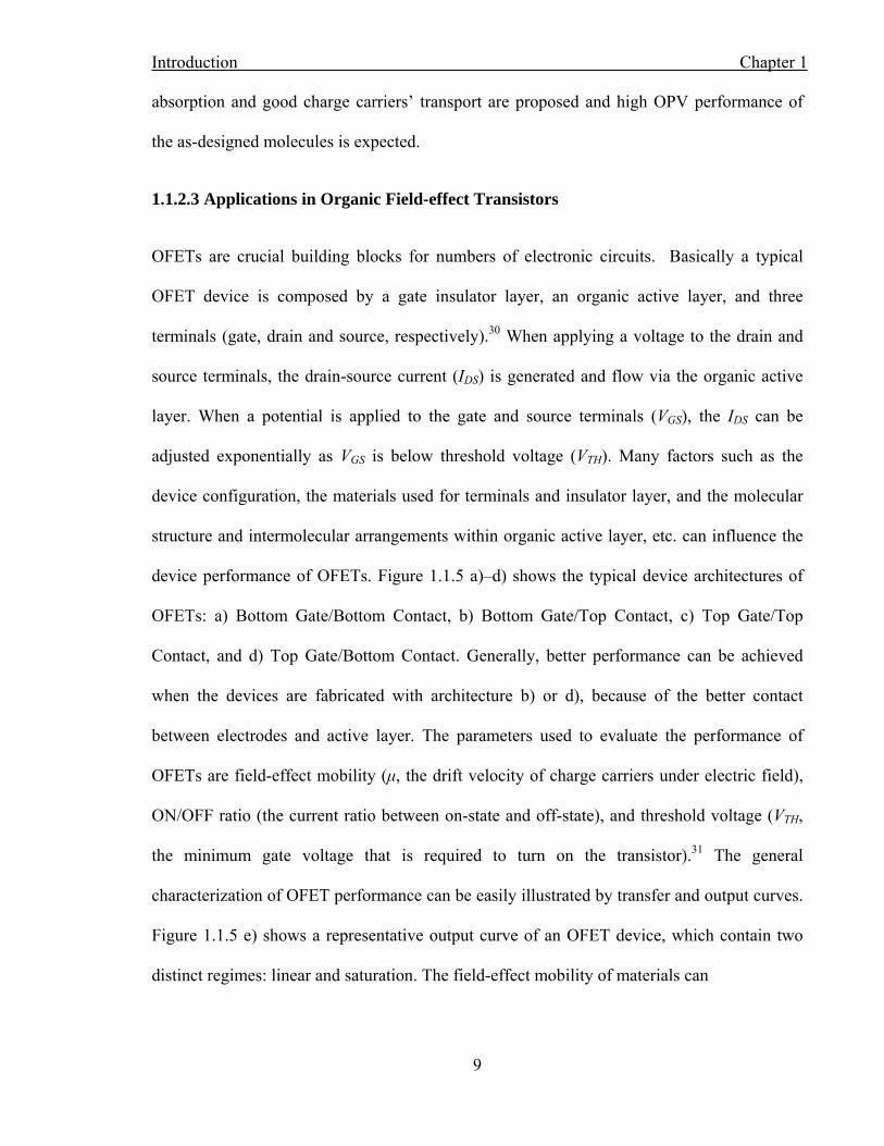
1.1.2.3 Applications in Organic Field-effect Transistors
OFETs are crucial building blocks for numbers of electronic circuits. Basically a typical
OFET device is composed by a gate insulator layer, an organic active layer, and three
terminals (gate, drain and source, respectively).30 When applying a voltage to the drain and
source terminals, the drain-source current (IDS) is generated and flow via the organic active
layer. When a potential is applied to the gate and source terminals (VGS), the IDS can be
adjusted exponentially as VGS is below threshold voltage (VTH). Many factors such as the
device configuration, the materials used for terminals and insulator layer, and the molecular
structure and intermolecular arrangements within organic active layer, etc. can influence the
device performance of OFETs. Figure 1.1.5 a)–d) shows the typical device architectures of
OFETs: a) Bottom Gate/Bottom Contact, b) Bottom Gate/Top Contact, c) Top Gate/Top
Contact, and d) Top Gate/Bottom Contact. Generally, better performance can be achieved
when the devices are fabricated with architecture b) or d), because of the better contact
between electrodes and active layer. The parameters used to evaluate the performance of
OFETs are field-effect mobility (μ, the drift velocity of charge carriers under electric field),
ON/OFF ratio (the current ratio between on-state and off-state), and threshold voltage (VTH,
the minimum gate voltage that is required to turn on the transistor).31 The general
characterization of OFET performance can be easily illustrated by transfer and output curves.
Figure 1.1.5 e) shows a representative output curve of an OFET device, which contain two
distinct regimes: linear and saturation. The field-effect mobility of materials can
Introduction Chapter 1
10
Figure 1.1.5 a) Bottom gate/bottom contact device. b) Bottom gate/top contact device. c) Top
gate/top contact device. d) Top gate/bottom contact device. e) Output characteristics and f)
transfer curves of a pentacene-based Bottom Gate/Top Contact OFET device (reproduced
based on literature).31,32
be extracted from the transfer curves (Figure 1.1.5 f)).32 Since the first report of OFET

Introduction Chapter 1
11
utilizing polythiophene as active layer in 1986, which achieved large modulation of IDS, the
searching for new high performance OFET materials has made large progress,33 and the
performance of OFETs has been improved immensely over the past decades, In contrast to
the conventional amorphous Si-based transistors, OFETs have reached comparable field-
effect mobility up to 1 cm2 V-1 s-1. However, the poor operational stability of OFETs limits
their practical application when the devices are exposed to ambient conditions, because
oxygen, moisture or light can act as performance degrading exponents. Such challenge is
particularly true for electron-transporting (n-type) OFETs. Actually, to date, few of n-type
materials are reported to own high electron mobility up to 1 cm2 V-1 s-1 in ambient conditions
with good stability. To develop air-stable n-type high mobility materials the molecules
should be highly electron-deficient systems, and the LUMO levels should be lower than -4.0
eV. Large N-heteroacenes with more N atoms doped in backbone can satisfy the
requirements and they are potential candidates to be developed as air-stable n-type materials.
1.2 Hypothesis
Different electron-deficient N-heteroacene units can be utilized to induce multiple
electron “traps”, and the strong electron-deficient N-heteroacene moieties can
generate multiple electrons intermolecular charge transfer in D-A molecules. The as-
prepared molecules, which are designed based on these rules, have the potential to be
developed as good performance multilevel ORM materials.
By verifying the structure, position and number of N atoms in N-heteroacenes, different
electron-deficient units can be achieved, which can be used as acceptor moieties in D-A
molecules. The various electron-deficient N-heteroacene units can play as multiple electron

Introduction Chapter 1
12
“traps” to induce multilevel memory behavior. Compared with other reported multilevel
memory materials, whose electron “traps” are induced by dispersed electron-withdrawing
groups, the acceptor moiety formed by N-heteroacene units can be conjugated together. On
the other hand, D-A molecules with strong electron-deficient N-heteroacenes as acceptors
can possibly accept multiple electrons to generate multiple electrons intermolecular charge
transfer. Considering the charming semiconducting properties of conjugated N-heteroacenes
in organic electronics, good multilevel memory performance is expected for materials
designed in these strategies.
Large conjugated N-heteroacenes can be used as acceptor moiety to build up D-π-A
molecules for high performance OPV application.
As pushing up the length of N-heteroacenes, their conjugation will be increased as well. The
D-π-A molecules with this type of N-heteroacenes as acceptor moieties are feasible due to
their broad absorption in visible region, which contributes to better sunlight harvesting and
charge carriers generation. In addition, with the increase of conjugation, the π-π interaction
between adjacent molecules will be enhanced, which is favored for the facilitation of charge
carrier transport. Thus the molecules designed in this strategy are expected to own high OPV
performance.
Large conjugated N-heteroacenes with more N atoms doped in backbone are expected
to own lower LUMO levels and applied as high performance air-stable n-type OFET
materials.
As the conjugation of N-heteroacenes is increased, the optical band gap of the molecules
become narrower, which will further lower the LUMO level in certain extents. Besides, by

Introduction Chapter 1
13
increasing the conjugation, more N atoms can be introduced into the backbone of molecules,
and the whole molecule can be developed as a highly electron-deficient system with
dramatically decreased LUMO levels. With the two aspects, the N-heteroacenes with LUMO
levels lower than -4.0 eV can be probably achieved as air-stable n-type OFET materials with
good performance.
1.3 Objectives
The first objective of this dissertation is to design and synthesize a series of D-A
molecules with conjugated N-heteroacenes as acceptor moieties, which can be applied
as multilevel rewritable ORM materials with high ON/OFF ratio, good endurance and
retention performance.
The key point of this objective is the acceptor engineering through combining different
electron-deficient N-heteroacene units or synthesizing strong electron-deficient N-
heteroacenes as acceptor moieties in D-A molecules. Suitable side chains will be connected
to the molecules to ensure that they can be processed by a solution-processing method. The
molecules will be characterized with common physical and chemical strategies. Typical MIM
ORMs will be fabricated based on the novel molecules to investigate their memory
performance. Molecular calculation will be utilized to study the switching mechanism in
order to investigate the structure-property relationship, and we expect to find out efficient
molecular designing strategies for developing multilevel rewritable ORM materials with high
ON/OFF ratio, good endurance and retention performance.

Introduction Chapter 1
14
The second objective of this dissertation is to design and synthesize D-π-A molecules
with large conjugated N-heteroacenes as acceptor moieties which can be used as high
performance OPV materials.
Large N-heteroacenes that would have more than three rings fused together to make large
conjugated acceptor moiety will be developed. Side chains engineering will be carried out to
ensure that the molecules have good solubility for solution process. The molecules will be
characterized with common physical and chemical strategies. Typical BHJ OPVs based on
the novel molecules will be fabricated and their OPV performance will be investigated. Both
molecular simulation and morphology analysis will be used to investigate the structure-
property relationship, and efficient molecular designing strategies for developing high
performance OPV materials with large conjugated N-heteroacenes as acceptors are expected.
The third objective of this dissertation is to design and synthesize large conjugated
highly electron-deficient N-heteroacenes which can be applied as air-stable n-type
OFET materials.
Long and linearly-fused large conjugated electron-deficient N-heteroacenes with LUMO
levels lower than -4.0 eV will be designed and synthesized. Certain side chains will be
attached onto the molecules to ensure they have good solubility in solution and orderly
stacking in solid states. The molecules will be characterized with common physical and
chemical strategies. Single crystal OFETs will be fabricated and the corresponding device
performance will be evaluated. Theoretical calculation will be carried out to study the
structure-property relationship, and a new family of air-stable, good performance n-type
OFET materials is expected.
Introduction Chapter 1
15
1.4 Scope
In this dissertation, the D-A and D-π-A molecules will be synthesized with originally
designed N-heteroacene acceptor moieties and widely investigated donor units. The large
conjugated electron-deficient N-heteroacenes will incorporate more N atoms in the backbone
of oligoacenes. All the synthesis will start from commercially available regents and solvents,
and the target molecules will be prepared through multiple-step organic reaction.
Physical and chemical characterization will be carried out after the synthesis of molecules.
HR MS, including ESI and MALDI-TOF will be used to characterize the molecular formula
and molecular weight of novel molecules. NMR will be applied to determine the molecular
structure. UV-vis absorption spectroscopy will be utilized to analyze the optical properties of
molecules, cyclic voltammetry (CV) analysis and electron ionization energy analysis will be
used to study the electrochemical properties. X-ray crystallographic analysis will be used to
study the molecular stacking behavior in crystals. Powder XRD patterns will be used for
analysis of molecular stacking in micro crystals. TEM and SAED will be conducted to
investigate the packing orientation of molecules in micro crystals. AFM will be used to study
the morphology of films. Out-of-plane XRD pattern will be carried out to investigate the
crystallinity of thin films. Molecular simulation and theoretical calculation will be carried out
to compute the electron distribution of molecules in frontier orbits and help to explain the
mechanisms of experimental results.
All the devices will be fabricated with solution processing method and standard
characterization strategies. MIM architecture ORM devices will be fabricated, and the
corresponding I-V curves, ON/OFF ratio, endurance and retention performance will be

Introduction Chapter 1
16
evaluated. BHJ architecture OPV devices with ITO/anode buffer layer/active layer/cathode
structure will be fabricated, the corresponding J-V and EQE curves, PCE, Jsc, Voc and FF will
be evaluated. Bottom Gate/Top Contact architecture OFET devices will be fabricated, and
the corresponding transfer and output characteristics, field-effect mobility, ON/OFF ratio,
VTH and environmental stability will be evaluated.
1.5 References
1 Chiang, C. K. Fincher, C. R. Park, Y. W. Heeger, A. J. Shirakawa, H. Louis, E. J.
Gau, S. C. & MacDiarmid, Alan G. Physical Review Letters 39, 1098-1101, (1977).
2 Xing, Q. Pei, W., Xu, R. & Pei, J. Fundamental Organic Chemistry (3Ed), Beijing:
Higher Education Press, (2005).
3 Miao, S. Brombosz, S. M. Schleyer, P.v.R. Wu, J. I. Barlow, S. Marder, S. R.
Hardcastle, K. I. & Bunz, U. H. F. Journal of the American Chemical Society 130,
7339-7344, (2008).
4 Wu, J. I., Wannere, C. S., Mo, Y., Schleyer, P. v. R. & Bunz, U. H. F. Journal of
Organic Chemistry 74, 4343-4349, (2009).
5 Scott, J. C. & Bozano, L. D. Nonvolatile memory elements based on organic
materials. Advanced Materials 19, 1452-1463, (2007).
6 Gregor, L. V. Thin Solid Films 2, 235-246, (1968).
7 Wang, C. Wang, J. Li, P.-Z. Gao, J. Tan, S. Y. Xiong, W.-W. Hu, B. Lee. P. S. Zhao,
Y. & Zhang, Q. Chemistry-an Asian Journal 9, 779-783, (2014).

Introduction Chapter 1
17
8 Li, H. Xu, Q. Li, N. Sun, R. Ge, J. Lu, J. Gu, H. & Yan, F. Journal of the American
Chemical Society 132, 5542-5543, (2010).
9 Ye, C. Q. Peng, Q. Li, M. Z. Luo, J. Tang, Z. M. Pei, J. Chen, J. M. Shuai, Z. G. Jiang,
L. & Song, Y. L. Journal of the American Chemical Society 134, 20053-20059,
(2012).
10 Gu, P. Y. Zhou, F. Gao, J. Li, G. Wang, C. Xu, Q. F. Zhang, Q. & Lu, J. M. Journal
of the American Chemical Society 135, 14086-14089, (2013).
11 Simao, C. Torrent, M. M. Montenegro, J. C. Oton, F. Veciana, J. & Rovira,
C. Journal of the American Chemical Society 133, 13256-13259, (2011).
12 Lee, W.-Y. Kurosawa, T. Lin, S. T. Higashihara, T. Ueda, M. & Chen, W.-Z.
Chemistry of Materials 23, 4487-4497, (2011).
13 Ling, Q. D. Chang, F.-C. Song, Y. Zhu, C.-X. Liaw, D.-J. Chan, D. S.-H. Kang, E.-T.
& Neoh, K.-G. Journal of the American Chemical Society 128, 8732-8733, (2006).
14 Chen, J. S. & Ma, D. G. Applied Physics Letters 87, 023505, (2005).
15 Mishra, A. & Baeuerle, P. Angewandte Chemie-International Edition 51, 2020-2067,
(2012).
16 Becquerel, A. E. Comptes rendus hebdomadaires des séances de l'Académie des
Sciences 561, (1839).
17 Halls, J. J. M. Walsh, C. A. Greenham, N. C. Marseglia, E. A. Friend, R. H. Moratti,
S. C. & Holmes, A. B. Nature 376, 498-500, (1995).

Introduction Chapter 1
18
18 Yu, G. Gao, J. Hummelen, J. C. Wudl, F. & Heeger, A. J. Science 270, 1789-1791,
(1995).
19 Tang, C. W. Applied Physics Letters 48, 183-185, (1986).
20 Zhang, Q. Kan, B. Liu, F. Long, G. Wan, X. Chen, X. Zuo, Y. Ni, W. Zhang, H. Li,
M. Hu, Z. Huang, F. Cao, Y. Liang, Z. Zhang, M. Russell, T. P. & Chen, Y. Nature
Photonics 9, 35-41, (2015).
21 Janssen, R. A. & Nelson, J. Advanced Materials 25, 1847-1858, (2013).
22 Ye, L. Zhang, S. Huo, L. Zhang, M. & Hou, J. Accounts of Chemical Research 47,
1595-1603, (2014).
23 Wang, E. Mammo, W. & Andersson, M. R. Advanced Materials 26, 1801-1826,
(2014).
24 Dou, L. You, J. Hong, Z. Xu, Z. Li, G. Street, R. A. & Yang, Y. Advanced Materials
25, 6642-6671, (2013).
25 Lai, Y.-Y. Cheng, Y.-J. & Hsu, C.-S. Energy & Environmental Science 7, 1866-1883,
(2014).
26 Lin, Y. Li, Y. & Zhan, X. Chemical Society Reviews 41, 4245-4272, (2012).
27 Shen, S. Jiang, P. He, C. Zhang, J. Shen, P. Zhang, Y. Yi, Y. Zhang, Z. Li, Z. & Li, Y.
Chemistry of Materials 25, 2274-2281, (2013).
Introduction Chapter 1
19
28 Love, J. A. Proctor, C. M. Liu, J. Takacs, C. J. Sharenko, A. Poll, T. S. Heeger, A. J.
Bazan, G. C. & Nguyen, T. Q. Advanced Functional Materials 23, 5019-5026, (2013).
29 Shin, J. Kang, N. S. Kim, K. H. Lee, T. W. Jin, J.-I. Kim, M. Lee, K. Ju, B. K. Hong,
J. M. & Choi. D. H. Chemical Communications 48, 8490-8492, (2012).
30 Wang, C. Dong, H. Hu, W. Liu, Y. & Zhu, D. Chemical Reviews 112, 2208-2267,
(2012).
31 Zhao, Y. Guo, Y. & Liu, Y. Advanced Materials 25, 5372-5391, (2013).
32 Wu, W. Liu, Y. & Zhu, D. Chemical Society Reviews 39, 1489-1502, (2010).
33 Tsumura, A. Koezuka, H. & Ando, T. Applied Physics Letters 49, 1210-1212, (1986).

N-heteroacenes for Organic Memories Chapter 2
20
Chapter 2
N-heteroacenes for Organic Memories
2.1 Literature Review
Polymer materials have been widely investigated in ORMs, while few of them displayed
multilevel memory behavior.1-10 A breakthrough was achieved by Li’s group, who reported
the protonic acid doped polymer 1 (Figure 2.1.1 a)) and the corresponding memory
properties.11 In their contribution, polyazomethine was synthesized firstly and the as-
prepared polymer was doped by p-toluenesulfonic acid (TsOH). Pt was used as top and
bottom electrodes to avoid filamentary effect in their ORM devices, which showed multilevel
memory behavior by controlling the “RESET” voltage (shown in Figure 2.1.1 b)) with
reasonable ON/OFF ratio between neighboring states (> 10) if the devices were only “SET”
to three states. The devices can be switched for more than 103 cycles between each state with
narrow distribution of resistance, showing charming endurance performance with good
uniformity. However, with the resistance of devices decreasing, the retention time decreased
accordingly. The authors believed that the protonic acid doping of a poly(schiff base) was a
energetically unfavorable process, which explained the bad retention performance of the
doped polymer. The multilevel memory behavior was proposed to be induced by electric-
field induced doping/dedoping effect. Later, Zhang’s group developed a polyoxometalate
(POM) based inorganic-organic hybrid polymer 2 (Figure 2.1.1 a)) with multilevel memory
behavior.12 ORM devices were fabricated with Pt as top electrode and ITO as bottom
electrode, similar to 1, the multiple resistance states were achieved by controlling the
“RESET” voltage. The device can only be switched between the three states for less than 20

N-heteroacenes for Organic Memories Chapter 2
21
Figure 2.1.1 a) Molecular structure of representative multilevel ORM polymers. b) I-V curves
for 1. c) I-V curves for 2 (reproduced based on literature).11,12
cycles with ON/OFF ratio at ~5, although each state can be retentive for more than 104
seconds. The authors believed that the multiple redox process in POM induced by various
electronic fields was responsible to the different resistance levels, which changes the charge
carrier density.
As the investigation of polymers, organic small molecules have been studied for application
in ORMs as well, and most of them displayed two-state memory behaviors.13-15 In 2010, Lu’s
group and Gu’s team collaborated together to present the first multilevel memory behaviors
of a series of small molecules (1–4 in Figure 2.1.2), the ORM devices with Al as top
electrode and ITO as bottom electrode showed three distinct resistance states with ON/OFF
ratio larger than 102, which was high enough for practical application. Different from

N-heteroacenes for Organic Memories Chapter 2
22
Figure 2.1.2 Molecular structures of representative multilevel ORM small molecules.
multilevel polymers, the resistances of molecules 1–4 were tuned step-by-step in set process,
with typically write-once-read-many-times (WORM) characteristics.16 All the three
resistance states were well retentive. Later in 2012 continued with this work, Lu’s group
designed two small molecules (5–6 in Figure 2.1.2) with different planarity of donor units.
However, the difference of ORMs between 1–4 and 5–6 only displayed in ON/OFF ratio.17
Rewritable multilevel small molecule (7 in Figure 2.1.2) was reported by Song’s group,18
which had a typical D-π-A structure with triphenylamine (TPA) as a donor and 2-
dicyanomethylen-3-cyano-4,5,5-trimethyl-2,5-dihydrofuran (TCF) as an acceptor. The
N-heteroacenes for Organic Memories Chapter 2
23
Figure 2.1.2 a) Representative I-V curves of a ternary WORM type ORM. b) I-V curves of
ORM based on molecule 7 (reproduced based on literature).16,18
memory devices utilized Al as top electrode and ITO as bottom electrode. Interestingly, in
dark conditions, the devices only showed two-state memory behavior, but under UV light,
three states memory behavior could be observed. The device could be “SET” or “RESET” to
different resistance states by controlling the “SET” and “RESET” voltage step-by-step with

N-heteroacenes for Organic Memories Chapter 2
24
charming ON/OFF ratio (> 102). Although the three states were well retentive, the authors
did not investigate the endurance performance of the devices. Large π conjugated N-
heteroacenes had also been investigated (8–9 in Figure 2.1.2).19,20 The molecules had
multiple electron-withdrawing groups (pyrazine and nitro groups in 8, pyrazine and cyano
groups in 9). The devices architecture and memory behavior based on the two molecules
were similar with 1–4, which were ternary and WORM type. All the authors believed that the
different electron withdrawing groups in these molecules played as multiple electron “traps”,
which could be filled at different “SET” voltage inducing the multilevel memory behavior.
However, the rewritable ability and endurance performance were key limits for their practical
application. Developing multilevel, rewritable, endurable and well retentive memory
materials are still challenging and in urgent demand.
2.2 D-A Molecules with Different N-heteroacene Units as Acceptor Moiety
2.2.1 Molecular Design
Considering different N-heteroacene units own various electron-withdrawing abilities, it
might be feasible to fuse multiple N-heteroacene units, an imidazole and a pyrazine into one
molecule to play as a single acceptor moiety. Such design might generate multiple electron
“traps”. Moreover, TPA can be selected as donor unit in memory materials because it has the
strong ability to stabilize charge separated state. To ensure the devices can be fabricated
through solution processing method, side chains are required to attach on the backbone of
molecules to help increase the solubility of the as-designed compounds in common organic
solvents. Triisopropylsilyl (TIPS) has been widely proven to be a perfect substituted group,
because the bulk spherical configuration with diameter at ~7 Å can lower the π-π interaction

N-heteroacenes for Organic Memories Chapter 2
25
of molecules in solution, which enhances their solubility efficiently. Besides that, attaching
TIPS to molecules can facilitate the 2D stacking of molecules in solid states so as to increase
π-overlap between adjacent molecules.21 With these considerations, we propose a novel D-A
molecule 4-(diphenylamino)phenyl-4,11-bis((triisopropylsilyl)ethynyl)-1H-imidazo[4,5-
b]phenazine (TPA-BIP), which has TPA as a donor unit and 4,11-
bis((triisopropylsilyl)ethynyl)-1H-imidazo[4,5-b]phenazine (BIP) as acceptor moiety with
two electron “traps”.
Figure 2.2.1.1 Molecular structure of TPA-BIP.
2.2.2 Synthesis of TPA-BIP
The synthetic route for TPA-BIP is illustrated in Scheme 2.2.2.1.
Synthesis of TAP
The intermediate diamine 1,4-bis((triisopropylsilyl)ethynyl)-2,3-diaminophenazine (TAP)
was synthesized according to a literature reported procedure.22 The commercially available
2,3-diaminophenazine was treated with iodine monochloride in anhydrous tetrahydrofuran
(THF) under N2 atmosphere to produce 1,4-iodine substituted compound 11. The two amino

N-heteroacenes for Organic Memories Chapter 2
26
Scheme 2.2.2.1 Synthetic route for TPA-BIP.
groups of 11 were protected by tert-butoxycarbonyl (Boc) to give compound 12. Sonogashira
coupling between 12 and TIPS acetylene produced compound 13, which was deprotected by
trifluoroacetic acid (TFA) to generate TAP as golden yellow solid in yield of ~19%.
Synthesis of TPA-BIP
In a 100 ml round bottom flask, TAP (550.27 mg, 0.96 mmol) and commercially available4-
(diphenylamino)benzaldehyde 14 (283.62 mg, 1.04 mmol) were well dissolved in
nitrobenzene (10 mL). The system was heated at 180 °C for 48 hours. After that, the system

N-heteroacenes for Organic Memories Chapter 2
27
was cooled down to room temperature and nitrobenzene was removed by reduced pressure
distillation method. The solid residue was obtained as crude product and further purified by
flash column chromatography with ethyl acetate (EtOAc) and hexane (EtOAc: hexane = 1:
20) over silica gel, the pure TPA-BIP (140 mg) was afforded as dark red powder in yield of
17%.
2.2.3 Molecular Characterization
The novel TPA-BIP had been characterized by HR MS, NMR and X-ray crystallographic
analysis.
2.2.3.1 HR MS Analysis
Figure 2.2.3.1.1 HR MS (ESI) spectra of TPA-BIP.
The HR MS (ESI) spectra of TPA-BIP were recorded on a Waters Q-Tof premierTM mass
spectrometer.
The chemical formula of TPA-BIP is C53H61N5Si2. As shown in Figure 2.2.3.1.1, the
calculated m/z value of [M+1]+ for TPA-BIP is 824.4544, and the actual m/z value of that
found in spectra is 824.4563, which is well consistent with the calculated result.

N-heteroacenes for Organic Memories Chapter 2
28
2.2.3.2 NMR Analysis
1H NMR and 13C NMR spectra of TPA-BIP were recorded on a Bruker 300-MHz
spectrometer.
Figure 2.2.3.2.1 1H NMR spectra of TPA-BIP in CD2Cl2.
The 1H NMR spectra were collected in CD2Cl2. As shown in Figure 2.2.3.2.1, the protons can
be indexed as 1H NMR (300 MHz, CD2Cl2, 298 K): δH = 1.21~1.42 (42H), 6.90~7.13 (4H),
7.02~7.25 (2H), 7.17~7.39 (6H), 7.66~7.87 (2H), 8.11~8.35 (4H), which are well
corresponding to the molecular structure.

N-heteroacenes for Organic Memories Chapter 2
29
Figure 2.2.3.2.2 13C NMR spectra of TPA-BIP in CDCl3.
The 13C NMR spectra of TPA-BIP were collected in CDCl3. As shown in Figure 2.2.3.2.2,
the carbon atoms can be indexed as 13C NMR (75 MHz, CDCl3, 298 K): δC = 157.37, 152.00,
145.80, 142.88, 141.75, 130.02, 129.84, 126.46, 125.34, 119.35, 119.26, 106.93, 106.88,
100.39, 19.20, 11.83. The carbons located at 11.83 and 19.20 are corresponded to TIPS
group, and only 14 carbons can be observed in range of 100–160 ppm, which is 3 carbons
less than theoretical value. Maybe certain carbons of TPA-BIP have no signals in 13C NMR
spectra in our experimental conditions.

N-heteroacenes for Organic Memories Chapter 2
30
2.2.3.3 Crystal Analysis
Figure 2.2.3.3.1 Images of a) top view & b) side view of TPA-BIP crystals.
Sheet-like single crystals of TPA-BIP were obtained in CH2Cl2 solution through slowly
evaporation method. Figure 2.2.3.3.1 shows the top and side view of the crystals. Single-
crystal XRD data was collected on a SuperNova CCD diffractometer at 293 K, which used
graphite-monochromated CuKα radiation (λ = 1.5418 Å). The direct method was used to
resolve the molecular structure, which was refined by full-matrix least-squares cycles in
SHELX-97. The anisotropic thermal parameters were utilized to refine all of the non-
hydrogen atoms. The hydrogen atoms were located at geometrically calculated positions and
were not refined, which were omitted for illustration convenience.
As shown in Figure 2.2.3.3.2 a) & b), it is clear that TPA has a twisted conformation from
both top and side view, which probably induces a bit of twist in BIP moiety. Demonstrated
from Figure 2.2.3.3.2 c), TPA-BIP adopts offset 2D face-to-face stacking between
neighboring molecules, but because of the twisted conformation of TPA, the molecules can
not stack perfectly in parallel. The intermolecular distance between adjacent molecules is 3.3
Å and 3.4 Å, respectively, which is shorter than that of van der Waals bond, indicating the
existence of strong π-π interactions. Both the 2D face-to-face stacking and strong π-π

N-heteroacenes for Organic Memories Chapter 2
31
Figure 2.2.3.3.2 a) Top view and b) side view of TPA-BIP crystal structure. c) Molecular
stacking of TPA-BIP.
interactions can contribute to the orderly arrangement of TPA-BIP in solid state, which is
probable to facilitate charge carriers’ transport.
2.2.3.4 Optical Properties of TPA-BIP
The optical properties of TPA-BIP were investigated through UV-vis absorption spectra,
which were recorded on a Shimadzu UV-2501 spectrophotometer. Figure 2.2.3.4.1 shows the
normalized UV-vis absorption spectra of TPA-BIP in CH3CN (red line) and in film (blue

N-heteroacenes for Organic Memories Chapter 2
32
Figure 2.2.3.4.1 Normalized UV-vis absorption spectra of TPA-BIP in CH3CN (red line) and
in film (blue line).
line). TPA-BIP exhibits a broad absorption band in visible region with the maximum
absorption wavelength (λmax) at 467 nm in CH3CN. The optical band gap (Eg) is determined
to be 2.17 eV from the onset absorption wavelength (λonset) at 572 nm, based on the equation
Eg = hc/λonset, where h is the Planck constant (6.63 × 10⁻³⁴ m2kg/s), c is the speed of light (3 ×
108 m/s). The λmax at 467 nm is largely red-shifted to 509 nm when TPA-BIP going from
solution to film, and a new absorption band with λmax at 545 nm appears. The λonset at 572 nm
is largely red-shifted to 593 nm in film as well. All the red shifts of λmax and λonset together
with the appearance of new absorption band suggest the stronger molecular interaction of
TPA-BIP in solid state.
2.2.3.5 Electrochemical Properties of TPA-BIP
The electrochemical properties of TPA-BIP were investigated through cyclic voltammetric
(CV) curves, which were recorded on a CHI 604E Electrochemical Analyzer. Glassy carbon
N-heteroacenes for Organic Memories Chapter 2
33
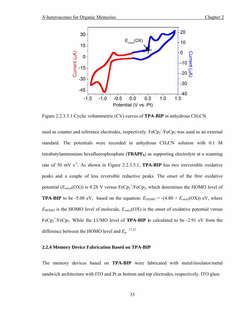
Figure 2.2.3.5.1 Cyclic voltammetric (CV) curves of TPA-BIP in anhydrous CH3CN.
used as counter and reference electrodes, respectively. FeCp2+/FeCp2 was used as an external
standard. The potentials were recorded in anhydrous CH3CN solution with 0.1 M
tetrabutylammonium hexafluorophosphate (TBAPF6) as supporting electrolyte at a scanning
rate of 50 mV s-1. As shown in Figure 2.2.3.5.1, TPA-BIP has two irreversible oxidative
peaks and a couple of less reversible reductive peaks. The onset of the first oxidative
potential (Eonset(OX)) is 0.28 V versus FeCp2+/FeCp2, which determines the HOMO level of
TPA-BIP to be -5.08 eV, based on the equation: EHOMO = -(4.80 + Eonset(OX)) eV, where
EHOMO is the HOMO level of molecule, Eonset(OX) is the onset of oxidative potential versus
FeCp2+/FeCp2. While the LUMO level of TPA-BIP is calculated to be -2.91 eV from the
difference between the HOMO level and Eg. 17,23
2.2.4 Memory Device Fabrication Based on TPA-BIP
The memory devices based on TPA-BIP were fabricated with metal/insulator/metal
sandwich architecture with ITO and Pt as bottom and top electrodes, respectively. ITO glass

N-heteroacenes for Organic Memories Chapter 2
34
Figure 2.2.4.1 a) AFM images of a 5 μm × 5 μm TPA-BIP film. b) Corresponding 3D AFM
images. c) XRD patterns of the corresponding film.
substrates were cleaned by ultrasonic in ethanol, acetone and isopropanol, respectively, and
dried under flowing N2. TPA-BIP was spin-coated onto pre-cleaned ITO glass substrates in
a solution of cyclohexanone (10 mg/mL) and dried at 120 °C on a hotplate. The thickness of
TPA-BIP film was measured to be ~120 nm by an Alpha-Step IQ Surface Profiler. To avoid
filamentary effect,24,25 Pt was sputter-coated on the top of organic layer through a shadow
mask with diameter at 100 μm. Tapping-mode AFM (Asylum Research Cypher S) was
carried out to investigate the morphology and microstructure of TPA-BIP film. Figure
2.2.4.1 a) shows the AFM height image of a 5 μm × 5 μm TPA-BIP film. The film is
crystalline with clear grain boundaries. The root-mean-square roughness (RMS) of TPA-BIP

N-heteroacenes for Organic Memories Chapter 2
35
film is 1.298 nm. Figure 2.2.4.1 b) shows the corresponding 3D AFM height image. The film
rolls up and down within the range of -10 to 10 nm, suggesting the film is well continuous.
The XRD patterns of the corresponding film was recorded on D8/max2500 with Cu Ka
source (κ = 1.541 Å). As shown in Figure 2.2.4.1 c), a diffracton peak at 5.4° can be
observed with intensity ~8 × 10², corresponding to the AFM images.
2.2.5 Memory Characteristics of TPA-BIP
The memory characteristics of the ITO/TPA-BIP/Pt devices were demonstrated by current-
voltage (I-V) curves, which were measured in ambient conditions using Keithley 4200
semiconductor characterization system in the voltage sweeping model. As shown in Figure
2.2.5.1 a), in the low sweeping voltage of “Sweep 1”, the ITO/TPA-BIP/Pt device retains at
high resistance state (HRs). An instantaneously increase of current can be observed when the
voltage reaches threshold voltage (VTH), as a result, the new low resistance state (LRs) is
achieved. The transform of the device from HRs to LRs can define the process as a “SET”
action. After removing power supply or applying a dual sweep “Sweep 2” the device can
maintain the LRs. Thus, the ITO/TPA-BIP/Pt device is a typical non-volatile memory. In the
following negative sweep “Sweep 3”, the recovery of device from LRs to HRs can be
observed, and the process is served as “RESET” action. In the dual negative sweep “Sweep 4”
the device maintains the HRs. Based on the I-V curves illustrated above, the ITO/TPA-
BIP/Pt device can be regarded as a two-state rewritable non-volatile memory. The ON/OFF
ratio of the device is achieved to be 103 when read at 0.2 V, indicating the device will have
much less misreading possibility in practical applications.
The endurance performance of ITO/TPA-BIP/Pt devices was investigated by the typical

N-heteroacenes for Organic Memories Chapter 2
36
Figure 2.2.5.1 a) I-V curves of ITO/TPA-BIP/Pt device. b) Resistance distribution of 14
cycles. c) Retention performance of ITO/TPA-BIP/Pt device.
“SET”-“RESET” cyclic switching operations. Generally, the devices were able to be
repeatedly switched between HRs and LRs for more than 14 cycles. Figure 2.2.5.1 b) shows
the corresponding resistances distribution of 14 cycles when the device is read at 0.2 V. The
average ON/OFF ratio of the resistance magnitude between the HRs and the LRs is about 103,
which is corresponding to that deduced from I-V curves. The resistances of HRs and LRs are
well distributed in a narrow range. The average VTH of “SET” or “RESET” processes for the
14 cycles is 2.60 V or -1.45 V, respectively. The orderly stacking of TPA-BIP molecules in
film possibly contributes to the good endurance performance.
N-heteroacenes for Organic Memories Chapter 2
37
The retention performance of the device was evaluated by applying a reading voltage of -0.2
V to either LRs or HRs in ambient conditions. As shown in Figure 2.2.5.1 c), there is no
obvious current degradation for each state can be observed in 4000 s during the test. Based
on the retention evaluation, TPA-BIP has the potential to be used as a kind of stable memory
material.
2.2.6 Mechanism Discussion
Molecular calculation was conducted using the density functional theory (DFT) calculations
(B3LYP/6-31G*) in Gaussian 09 to describe the switching mechanism and the generated
charge carriers’ migration process of ITO/TPA-BIP/Pt devices.26,27 As shown in Figure
2.2.6.1, the LUMO coefficient of TPA-BIP is mainly located at the BIP moiety, while the
HOMO coefficient is distributed on the whole molecule. The difference between the HOMO
level of TPA-BIP and the working function of ITO (-4.8 eV) is 0.12 eV, which determines
the holes injection energy barrier. However, the electrons injection energy barrier is
established to be 2.74 eV based on the difference between the LUMO level of TPA-BIP and
the working function of Pt (-5.6 eV). Therefore, holes injection is dominated for the charge
carriers’ migration.
One possibility to inducing the memory behavior of TPA-BIP is the filling of electron
“traps”. Electrostatic potential (ESP) calculation of TPA-BIP was carried out with same
calculation method. As shown in Figure 2.2.6.2, the surface of TPA-BIP has continuous
positive ESP (in blue) with certain negative regions (in red), corresponding to imidazole and
pyrazine units, respectively, which serve as electron “traps’’ to block the mobility of charge
carriers. It is because of the electron “traps’’ and the energy barrier between molecules and

N-heteroacenes for Organic Memories Chapter 2
38
Figure 2.2.6.1 Electron density distribution of HOMO & LUMO levels of TPA-BIP.
electrodes that the conductivity of ITO/TPA-BIP/Pt devices is low in HRs. As the voltage
approaches to threshold value, the electrons “traps” will be filled so that electrons can exceed
the energy barrier. In this situation charge separation occurs and free charge carriers are
generated. As a result, the devices are set to LRs and the molecular surface of TPA-BIP
becomes continuous positive. It is noteworthy that the multiple electron “traps” can be
possibly filled in same time, thus the devices display only two-state memory behavior. The
corresponding non-volatile memory behaviour may come from the few release of charge
carriers.28,29 This mechanism has been well illustrated in azo-benzene based D-A molecules
by Lu’s group. Intermolecular charge transfer can also possibly induce the memory behavior
of TPA-BIP. Charge transfer complexes can be formed as charge carriers, in which situation
electrons migrates from the HOMO level of one molecule to the LUMO level of another
molecule. The as formed charge transfer complex can be stable without the existence of
electronic field, leading to non-volatile memory behavior.8 Kang’s group has used this type
of mechanism to explain the memory behavior for polyimide based D-A polymers.
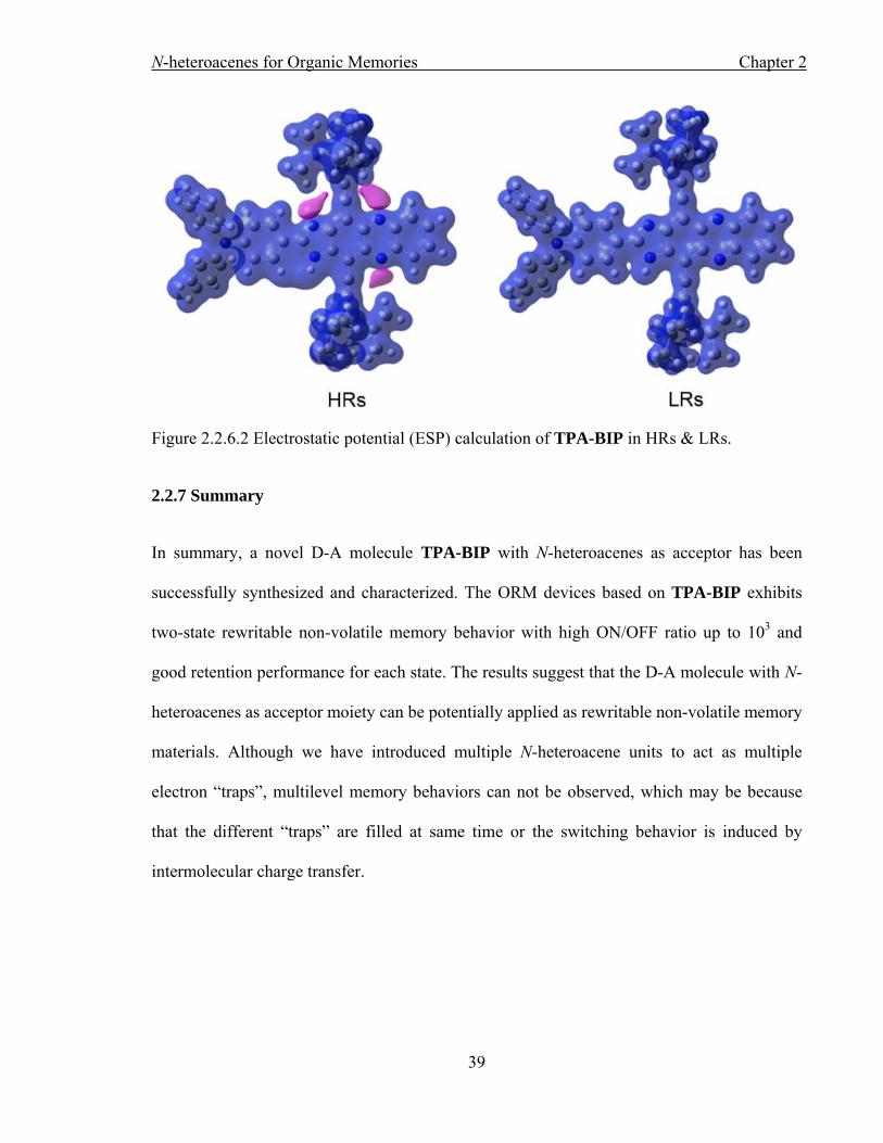
N-heteroacenes for Organic Memories Chapter 2
39
Figure 2.2.6.2 Electrostatic potential (ESP) calculation of TPA-BIP in HRs & LRs.
2.2.7 Summary
In summary, a novel D-A molecule TPA-BIP with N-heteroacenes as acceptor has been
successfully synthesized and characterized. The ORM devices based on TPA-BIP exhibits
two-state rewritable non-volatile memory behavior with high ON/OFF ratio up to 103 and
good retention performance for each state. The results suggest that the D-A molecule with N-
heteroacenes as acceptor moiety can be potentially applied as rewritable non-volatile memory
materials. Although we have introduced multiple N-heteroacene units to act as multiple
electron “traps”, multilevel memory behaviors can not be observed, which may be because
that the different “traps” are filled at same time or the switching behavior is induced by
intermolecular charge transfer.
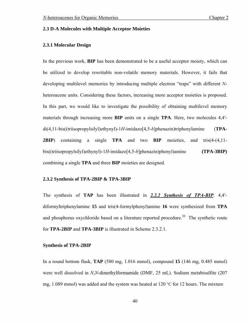
N-heteroacenes for Organic Memories Chapter 2
40
2.3 D-A Molecules with Multiple Acceptor Moieties
2.3.1 Molecular Design
In the previous work, BIP has been demonstrated to be a useful acceptor moiety, which can
be utilized to develop rewritable non-volatile memory materials. However, it fails that
developing multilevel memories by introducing multiple electron “traps” with different N-
heteroacene units. Considering these factors, increasing more acceptor moieties is proposed.
In this part, we would like to investigate the possibility of obtaining multilevel memory
materials through increasing more BIP units on a single TPA. Here, two molecules 4,4′-
di(4,11-bis((triisopropylsilyl)ethynyl)-1H-imidazo[4,5-b]phenazin)triphenylamine (TPA-
2BIP) containing a single TPA and two BIP moieties, and tris(4-(4,11-
bis((triisopropylsilyl)ethynyl)-1H-imidazo[4,5-b]phenazin)phenyl)amine (TPA-3BIP)
combining a single TPA and three BIP moieties are designed.
2.3.2 Synthesis of TPA-2BIP & TPA-3BIP
The synthesis of TAP has been illustrated in 2.2.2 Synthesis of TPA-BIP. 4,4′-
diformyltriphenylamine 15 and tris(4-formylphenyl)amine 16 were synthesized from TPA
and phosphorus oxychloride based on a literature reported procedure.30 The synthetic route
for TPA-2BIP and TPA-3BIP is illustrated in Scheme 2.3.2.1.
Synthesis of TPA-2BIP
In a round bottom flask, TAP (580 mg, 1.016 mmol), compound 15 (146 mg, 0.485 mmol)
were well dissolved in N,N-dimethylformamide (DMF, 25 mL). Sodium metabisulfite (207
mg, 1.089 mmol) was added and the system was heated at 120 °C for 12 hours. The mixture

N-heteroacenes for Organic Memories Chapter 2
41
Scheme 2.3.2.1 Synthetic route for TPA-2BIP and TPA-3BIP.
was poured into iced water (100 mL) after it was cooled down to room temperature. After
filtration, the solid residue was obtained as crude product, which was further purified by flash
column chromatography with EtOAc and hexane (EtOAc: hexane = 1: 20) over silica gel,
and finally the pure TPA-2BIP (97 mg) was obtained as dark red powder in yield of 6.9%.
Synthesis of TPA-3BIP
TPA-3BIP (73 mg) was prepared in same procedure illustrated above, with TAP (594 mg,
1.041 mmol), compound 16 (103 mg, 0.313 mmol) and sodium metabisulfite (216 mg, 1.139
mmol), as dark red powder in yield of 3.7%.

N-heteroacenes for Organic Memories Chapter 2
42
2.3.3 Molecular Characterization
The novel TPA-2BIP & TPA-3BIP have been characterized by HR MS and NMR.
2.3.3.1 HR MS Analysis
Figure 2.3.3.1.1 HR MS (ESI) spectra of TPA-2BIP.
The HR MS (ESI) spectra of TPA-2BIP were collected on a JEOL spiral TOF JMS-S3000
spectrometer.

N-heteroacenes for Organic Memories Chapter 2
43
The chemical formula of TPA-2BIP is C88H107N9Si4. As shown in Figure 2.3.3.1.1,
thecalculated m/z value of [M+1]+ for TPA-2BIP is 1402.7727, and the actual m/z value of
that found in spectra is 1402.7804, which is well consistent with the calculated result.
Figure 2.3.3.1.2 HR MS (MOLDI-TOF) spectra of TPA-3BIP.

N-heteroacenes for Organic Memories Chapter 2
44
The HR MS (MOLDI-TOF) spectra of TPA-3BIP were collected on the same machine with
TPA-2BIP.
The chemical formula of TPA-3BIP is C123H154N13Si6. As shown in Figure 2.3.3.1.2, the
calculated m/z value for TPA-3BIP is 1981.1021, and the actual m/z value found in spectra is
1981.1060, which is well consistent with the calculated result.
2.3.3.2 NMR Analysis
Figure 2.3.3.2.1 1H NMR spectra of TPA-2BIP in CDCl3.
1H NMR and 13C NMR spectra of TPA-2BIP and TPA-3BIP were recorded on a Bruker
400-MHz spectrometer in CDCl3.
N
HN
NN
NH
N
NN
N
Sii-Pr3
i-Pr3SiSii-Pr3
i-Pr3Si
TPA-2BIP
a b
cd
e
f
gh
a'
b'
d'e'

N-heteroacenes for Organic Memories Chapter 2
45
Figure 2.3.3.2.1 shows the 1H NMR spectra of TPA-2BIP in CDCl3, the protons can
indexed as 1H NMR (400 MHz, CDCl3, 298 K): δH = 1.28 (42H), 1.32 (42H), 7.22~7.24 (3H),
7.27~7.31 (4H), 7.38~7.44 (2H), 7.75~7.80 (4H), 8.10~8.14 (4H), 8.20~8.28 (4H), 9.54~9.58
(2H), which are well consistent with its molecular structure.
Figure 2.3.3.2.2 13C NMR spectra of TPA-2BIP in CDCl3.
Figure 2.3.3.2.2 shows the 13C NMR spectra of TPA-2BIP in CDCl3. The carbons can be
indexed as 13C NMR (101 MHz, CDCl3, 298 K): δC = 157.81, 150.76, 150.00, 146.31, 143.10,
142.14, 141.79, 141.73, 130.60, 130.22, 130.13, 129.56, 127.22, 126.32, 123.96, 123.03,
112.56, 106.68, 104.97, 101.96, 101.74, 100.86, 19.47, 12.22, 12.04. The carbons located at
12.04, 12.22 and 19.47 are corresponded to the two types of TIPS groups. There are only 22
carbons can be observed in range of 100–160 ppm, which is 5 carbons less than theoretical

N-heteroacenes for Organic Memories Chapter 2
46
value. Maybe certain carbons of TPA-2BIP have no signals in 13C NMR spectra in our
experimental conditions.
Figure 2.3.3.2.3 1H NMR spectra of TPA-3BIP in CDCl3.
Figure 2.3.3.2.3 shows the 1H NMR spectra of TPA-3BIP in CDCl3, the protons can be
indexed as 1H NMR (400 MHz, CDCl3, 298 K): δH = 1.28~1.30 (126H), 7.34~7.36 (6H),
7.76~7.81 (6H), 8.18~8.28 (12H), which are well consistent with its molecular structure.
Figure 2.3.3.2.4 shows the 13C NMR spectra of TPA-3BIP in CDCl3. The carbons can be
indexed as 13C NMR (101 MHz, CDCl3, 298 K): δC = 156.96, 149.25, 142.53, 141.30, 129.91,
129.71, 129.30, 124.76, 123.94, 105.56, 100.65, 18.84, 11.50. The carbons located at 11.50
and 18.84 are corresponded to the TIPS group, only 11 carbons can be observed in range of
N
HN
NN
NH
N
NN
N
Sii-Pr3
i-Pr3SiSii-Pr3
i-Pr3Si
NHN
NN
Sii-Pr3i-Pr3Si
TPA-3BIP
a b
cd
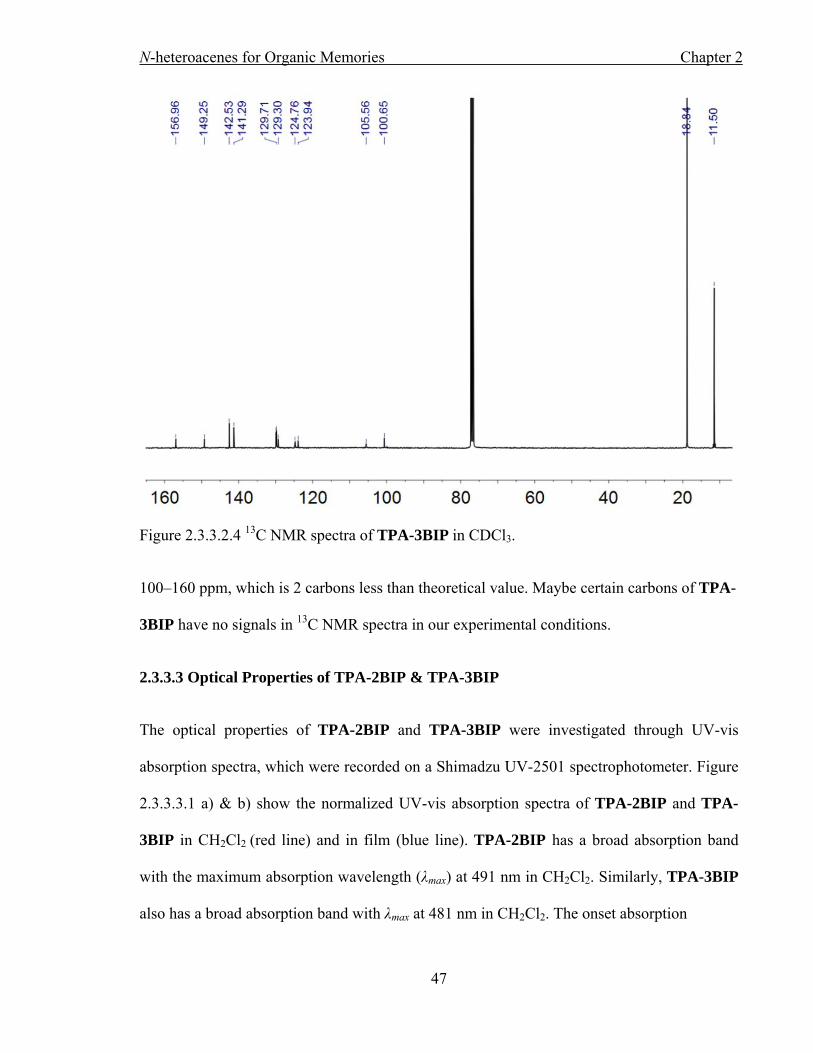
N-heteroacenes for Organic Memories Chapter 2
47
Figure 2.3.3.2.4 13C NMR spectra of TPA-3BIP in CDCl3.
100–160 ppm, which is 2 carbons less than theoretical value. Maybe certain carbons of TPA-
3BIP have no signals in 13C NMR spectra in our experimental conditions.
2.3.3.3 Optical Properties of TPA-2BIP & TPA-3BIP
The optical properties of TPA-2BIP and TPA-3BIP were investigated through UV-vis
absorption spectra, which were recorded on a Shimadzu UV-2501 spectrophotometer. Figure
2.3.3.3.1 a) & b) show the normalized UV-vis absorption spectra of TPA-2BIP and TPA-
3BIP in CH2Cl2 (red line) and in film (blue line). TPA-2BIP has a broad absorption band
with the maximum absorption wavelength (λmax) at 491 nm in CH2Cl2. Similarly, TPA-3BIP
also has a broad absorption band with λmax at 481 nm in CH2Cl2. The onset absorption

N-heteroacenes for Organic Memories Chapter 2
48
Figure 2.3.3.3.1 Normalized UV-vis absorption spectra of a) TPA-2BIP (red line: in solution,
blue line: in film) & b) TPA-3BIP (red line: in solution, blue line: in film).
wavelength of TPA-2BIP (λonset) is 563 nm, and the optical band gap (Eg) is determined to be
2.20 eV through the same equation illustrated in 2.2.3.4 Optical Properties of TPA-BIP. The
Eg for TPA-3BIP is established to be 2.22 eV from the λonset at 558 nm. Compared with
TPA-2BIP, both the λmax and λonset of TPA-3BIP in solution are blue-shifted, suggesting that
the energy gap of intramolecular electrons transition is enlarged as more acceptor moieties
introduced in molecules. The λonset of TPA-2BIP is red-shifted to 601 nm in film, and that of
TPA-3BIP is red-shifted to 617 nm, indicating that strong π-π stacking of molecules exists in
solid state. The red-shift of TPA-3BIP in film is 16 nm larger than that of TPA-2BIP,
suggesting that it may have stronger interaction between neighbouring molecules in solid
state.
2.3.3.4 Electrochemical Properties of TPA-BIP & TPA-3BIP
The electrochemical properties of TPA-2BIP and TPA-3BIP were investigated through
cyclic voltammetric (CV) curves, which were carried out in anhydrous CH2Cl2 with the same

N-heteroacenes for Organic Memories Chapter 2
49
Figure 2.3.3.4.1 Cyclic voltammetric (CV) curves of a) TPA-2BIP & b) TPA-3BIP in
anhydrous CH2Cl2.
method of TPA-BIP illustrated in 2.2.3.5 Electrochemical Properties of TPA-BIP. As
shown in Figure 2.3.3.4.1 a), TPA-2BIP displays one irreversible oxidative peak and one
irreversible reductive peak. The onset of the oxidative potential (Eonset(OX)) is 0.40 V versus
FeCp2+/FeCp2, and the HOMO level of TPA-2BIP is determined to be -4.94 eV, which is
calculated with the equation illustrated in 2.2.3.5 Electrochemical Properties of TPA-BIP.
The LUMO level is established to be -2.74 eV from the difference between HOMO level and
Eg. TPA-3BIP (Figure 2.3.3.4.1 b)) also exhibits one irreversible reductive peak, however,
there are two irreversible oxidative peaks can be observed. The potential versus
FeCp2+/FeCp2 of the first oxidative peak is 0.44 V, and with the same calculation method of
TPA-2BIP, the HOMO and LUMO levels are determined to be -4.98 eV and -2.76 eV,
respectively. Based on the CV curves and above analysis, there is no clear effect on the
reductive behavior of molecules when more acceptor moieties are attached, and it can be
further confirmed with the fact that TPA-2BIP and TPA-3BIP own close LUMO levels.
Increasing the acceptor moieties might have minor influence on the oxidative properties of

N-heteroacenes for Organic Memories Chapter 2
50
molecule, because a minor up-shift of Eonset(OX) of TPA-3BIP can be observed. Probably
the increase of acceptor moieties can cause the dispersing of electrons distribution, which
makes the electron-donating ability of donor unit weaker.
2.3.4 Memory Device Fabrication Based on TPA-2BIP & TPA-3BIP
The memory devices based on TPA-2BIP and TPA-3BIP were fabricated in the same
procedure with TPA-BIP illustrated in 2.2.4 Memory Device Fabrication Based on TPA-
BIP, the only difference was that the top electrode was changed from Pt to Au considering its
higher working function. The thickness of TPA-2BIP and TPA-3BIP films was measured to
be ~60 nm by an Alpha-Step IQ Surface Profiler.
The morphology and microstructure of TPA-2BIP and TPA-3BIP films were investigated
by tapping-mode AFM (Park Systems Co.). Figure 2.3.4.1 a) and c) show the corresponding
height images of AFM. The high crystalline of films with clear grain boundaries can be
observed for both TPA-2BIP and TPA-3BIP, however, the film of TPA-3BIP has the
smaller grain size than that of TPA-2BIP. The films for the two molecules are well smooth
with the root-mean-square roughness (RMS) at 1.496 nm for TPA-2BIP and 1.127 nm for
TPA-3BIP, respectively. The relatively smaller grain size and smoother surface of TPA-
3BIP film suggests that the stacking of molecules in solid state has been changed as the
acceptor moieties are increased to their backbone, which can possibly enhance the contact
between electrodes and organic films. Figure 2.3.4.1 b) & d) show the corresponding 3D
height images of AFM. The film of TPA-2BIP rolls up and down within the range of -4 to 8
nm, and that of TPA-3BIP is -4 to 4 nm, suggesting both the films are well continuous. The
XRD patterns of the films of TPA-2BIP and TPA-3BIP were investigated in same method
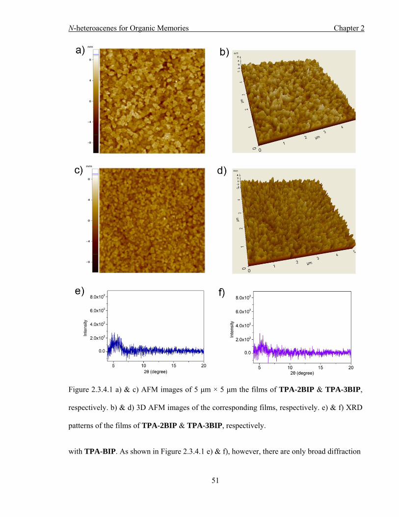
N-heteroacenes for Organic Memories Chapter 2
51
Figure 2.3.4.1 a) & c) AFM images of 5 μm × 5 μm the films of TPA-2BIP & TPA-3BIP,
respectively. b) & d) 3D AFM images of the corresponding films, respectively. e) & f) XRD
patterns of the films of TPA-2BIP & TPA-3BIP, respectively.
with TPA-BIP. As shown in Figure 2.3.4.1 e) & f), however, there are only broad diffraction

N-heteroacenes for Organic Memories Chapter 2
52
peaks in rang of 4°–7° with low intensity that can be observed. The films might be too thin
for XRD diffraction measurement.
2.3.5 Memory Characteristics of TPA-2BIP & TPA-3BIP
The memory properties of ITO/TPA-2BIP/Au and ITO/TPA-3BIP/Au devices were
characterised by current-voltage (I-V) curves, which were performed under the same
conditions with that of TPA-BIP illustrated in 2.2.5 Memory Characteristics of TPA-BIP.
As shown in Figure 2.3.5.1 a) ITO/TPA-2BIP/Au device. The current of ITO/TPA-2BIP/Au
device maintains in low magnitude range under low sweeping voltage in the first positive
sweep, whose state can be defined as high resistance state (HRs). The current is abruptly
increased to the magnitude of compliance (1 mA) at threshold voltage (VTH), in which
situation the device is switched to a low resistance state (LRs). The switching process can be
defined as a “SET” action. After removing voltage supply or apply a dual positive sweep
again the current can be maintain at LRs, suggesting that the ITO/TPA-2BIP/Au device is a
non-volatile type memory. The device can be recovered to its initial HRs from LRs in the
reverse sweep from 0 V to -2 V, and the recovery process is defined as a “RESET” action. As
shown in Figure 2.3.5.1 b), ITO/TPA-3BIP/Au device has similar switching behaviors with
ITO/TPA-2BIP/Au, but the current in HRs is ~10 times larger, indicating that ON/OFF ratio
is ~10 times smaller. Based on the I-V curves of ITO/TPA-2BIP/Au and ITO/TPA-3BIP/Au
devices and above analysis, there is little influence on the switching behavior by verifying the
acceptor moieties, but that is possibly able to induce different conductivity in HRs, thus,
result in different ON/OFF ratio. Combined with the UV-vis absorption spectra and height
images of AFM, the more ordered molecular stacking in solid state and the better contact
between electrodes and organic films can affect the conductivity of molecules to induce

N-heteroacenes for Organic Memories Chapter 2
53
Figure 2.3.5.1 a) & b) I-V curves, c) & d) resistance distribution, e) & f) retention
performance of the ITO/TPA-2BIP (or TPA-3BIP)/Au devices, respectively.
different ON/OFF ratio.

N-heteroacenes for Organic Memories Chapter 2
54
The endurance performance of ITO/TPA-2BIP/Au and ITO/TPA-3BIP/Au devices was
investigated by cyclic switching through the typical “SET”-“RESET” operations. Generally,
both TPA-2BIP and TPA-3BIP can be repeatedly switched between HRs and LRs for more
than 100 cycles. Figure 2.3.5.1 c) & d) show the corresponding resistances distribution of
each state when read at 0.1 V for 100 cycles. In LRs the resistances of both TPA-2BIP and
TPA-3BIP have a narrow distribution in range of 102–5 × 10² Ω. In HRs the resistances of
TPA-3BIP can still maintain narrow distribution in the range of 104–5 × 10⁴ Ω, however,
those of TPA-2BIP are distributed scatted in a wide range of 104–5 × 10⁵ Ω. The average
ON/OFF ratio device between HRs and LRs for the 100 cycles of ITO/TPA-2BIP/Au is ~4 ×
102, and that of ITO/TPA-3BIP/Au device is ~7 × 10, respectively. The ON/OFF ratio of
both TPA-2BIP and TPA-3BIP is high enough for practical application. The average VTH for
ITO/TPA-2BIP/Au and ITO/TPA-3BIP/Au devices have very close value, which is 0.83 V
and 0.84 V for “SET” process and -0.69 V and -0.66 V for “RESET” process, respectively.
The close average VTH is further corresponded to the fact that there is no significant effect on
the switching behaviors by changing the number of acceptor moieties.
The retention performances of ITO/TPA-2BIP/Au and ITO/TPA-3BIP/Au devices were
evaluated by applying a reading voltage of -0.1 V on both HRs and LRs in ambient
conditions. Figure 2.3.5.1 e) & f) show the corresponding evaluation results, no obvious
current decay can be observed for each state in 104 seconds during the test, indicating that
both the two states of the two types of device are well retentive.
2.3.6 Mechanism Discussion
Molecular calculation of TPA-2BIP and TPA-3BIP was carried out in same method with

N-heteroacenes for Organic Memories Chapter 2
55
TPA-BIP illustrated in 2.2.6 Mechanism Discussion (TMS ((trimethylsilyl)ethynyl)) groups
were used instead of TIPS for calculation convenience). Figure 2.3.6.1 a) shows the electron
density distribution of TPA-2BIP, the HOMO coefficient is dispersed on TPA and one BIP
moiety (A1), while the LUMO coefficient is mainly located on the other BIP moiety (A2).
The HOMO and LUMO levels of TPA-2BIP display a typical D-A distribution, although the
molecule owns an A-D-A structure. As shown in Figure 2.3.6.1 b), the HOMO coefficient of
TPA-3BIP is dispersed on the whole molecule, including the TPA unit and the three BIP
moieties, and the distribution of LUMO coefficient of TPA-3BIP is similar to TPA-2BIP.
Based on the calculation results, there is probably only one acceptor moiety of TPA-2BIP
and TPA-3BIP can act as the “real” acceptor, although both the two molecules have multiple
acceptor moieties. The energy barrier is estimated to be 2.36 eV between the LUMO level of
TPA-2BIP and the working function of Au (-5.1 eV), and that of TPA-3BIP is determined to
be 2.34 eV, respectively. In another hand, the energy barrier is 0.14 eV between the HOMO
level of TPA-2BIP and the working function of ITO (-4.8 eV), and that of TPA-3BIP is 0.18
eV, respectively. Thus, holes injection is dominated in charge carriers’ migration for the two
types of devices.
The memory behaviors of ITO/TPA-2BIP/Au and ITO/TPA-3BIP/Au devices can be
explained by electron “traps” mechanism. In HRs, the energy barriers and electron “traps”
induced by acceptor moieties of both TPA-2BIP and TPA-3BIP can block the electrons
injection and charge carriers migration. After the voltage is increased to VTH the electron
“traps” can be filled and the corresponding devices will be set to LRs. As illustrated in
previous section, only one acceptor moiety in TPA-2BIP or TPA-3BIP can act as “real”
acceptor moiety, therefore, only one electron “traps” will be filled in switching process. As a

N-heteroacenes for Organic Memories Chapter 2
56
Figure 2.3.6.1 Electron density distribution of a) TPA-2BIP & b) TPA-3BIP.
result, similar memory behaviors can be observed in ITO/TPA-2BIP/Au and ITO/TPA-
3BIP/Au devices. Intermolecular charge transfer occurring between HOMO and LUMO
levels of the two molecules can also demonstrate the switching mechanism of the two types
of devices, which can form charge transfer complex as charge carriers. The non-volatile
memory performance were probably coming from the stabilized charge carriers, which are
generated by filling of electron “traps” or intermolecular charge transfer.
N-heteroacenes for Organic Memories Chapter 2
57
2.3.7 Summary
Two D-A molecules TPA-2BIP and TPA-3BIP with a single TPA donor unit and various
number of BIP acceptor moieties have been synthesized and characterized. Sandwich
architecture memory devices have been fabricated with TPA-2BIP or TPA-3BIP as active
layer. Similar switching behaviors are observed and the two molecules own close threshold
voltage. The ON/OFF ratio of the two types of devices shows difference in magnitude of 10
times. The TPA-3BIP film has smaller grain size and is smoother than TPA-2BIP based on
the morphology analysis of active layers, which can explain its low ON/OFF ratio. The
similar switching process has been demonstrated to be induced by filling of electron “traps”
or intermolecular charge transfer, which can occur between the HOMO level of donor unit
and LUMO level of “real” acceptor moiety. In this part it is found that increasing acceptor
moieties does not generally induce multilevel memory behaviors, and the morphology of
active layer may can influence the ON/OFF ratio of devices.
2.4 D-A Molecules with Strong Electron-deficient N-heteroacene and Multiple Donors
2.4.1 Molecular Design
Considering the acceptors engineering including incorporation of multiple electron “traps”
through different N-heteroacene units and increasing the number of acceptor moieties does
not generally induce multilevel memory behaviors, we would like to design molecules from
another aspect. The rewritable memory behaviors in D-A molecules have also been proved to
be induced by intermolecular charge transfer, in which situation the recombination of charge
carriers can functionalize as “RESET” operation in switching process.8 An interesting issue is
whether multiple electrons intermolecular charge transfer can occur so that various charge

N-heteroacenes for Organic Memories Chapter 2
58
carriers’ generation can be obtained to adjust the resistance of certain materials, and besides
of that the rewritable memory performance can be possibly realized through different charge
carriers’ recombination, thus, rewritable multilevel memory materials are expected. To
achieve this concept, multiple donor units with strong electron-deficient acceptor in one
molecule can be a solution. We propose a novel tetraazatetracene derivative 2,3-(4,4'-
bis(N,N-diphenylamino)benzyl)-5,12-bis((triisopropylsilyl)ethynyl)-1,4,6,11-
tetraazatetracene (2TPA-BTTT), which contains two TPA units as donors and 5,12-
bis((triisopropylsilyl)ethynyl)-1,4,6,11-tetraazatetracene (BTTT) as an acceptor.
2.4.2 Synthesis of 2TPA-BTTT
The synthesis of TAP has been illustrated in 2.2.2 Synthesis of TPA-BIP. The synthetic
route for 2TPA-BTTT is illustrated in Scheme 2.4.2.1.
Scheme 2.4.2.1 Synthetic route for 2TPA-BTTT.
Synthesis of 4,4'-bis(N,N-diphenylamino)benzil 17

N-heteroacenes for Organic Memories Chapter 2
59
In a round bottom flask, anhydrous aluminum chloride (1335 mg, 10 mmol) was suspended
in anhydrous CH2Cl2 (50 mL), oxalyl chloride (646 mg, 5 mmol) was added in one portion,
and TPA (2940 mg, 12 mmol) was added in several small portions. The system was heated to
reflux for 6 hours. After that the system was cooled down to room temperature, quenched by
pouring the solution into iced water. Hydrochloric acid (37%, 10 mL) was added to the
mixed solution and stirred for 10 minutes. After that, the organic layer was collected, and the
aqueous layer was extracted twice with CH2Cl2 (20 mL). The combined organic phases were
washed with water and brine, and dried over anhydrous Na2SO4. The pure compound 17
(1710 mg) was obtained after flash column chromatography over silica gel with CH2Cl2 and
hexane (CH2Cl2: hexane = 1: 1) as yellow powder in yield of 65%.
Synthesis of 2TPA-BTTT
In a round bottom flask, TAP (1215.3 mg, 2.12 mmol) and 17 (530.4 mg, 0.98 mmol) were
dissolved in acetic acid (20 mL), and 2-iodoxybenzoic acid (IBX, 7.5 mg) was added in one
portion. The system was heated to reflux for 48 hours under Argon atmosphere. After that the
solution was cooled down to room temperature and poured into iced water. After filtration,
the solid residue was obtained as crude product, which was further purified by flash column
chromatography with EtOAc and hexane (EtOAc: hexane = 1: 20) over silica gel to afford
pure 2TPA-BTTT (137.0 mg) as dark blue powder in yield of 13%.
2.4.3 Molecular Characterization
2TPA-BTTT has been characterized with HR MS, NMR and X-ray crystallographic
analysis.

N-heteroacenes for Organic Memories Chapter 2
60
2.4.3.1. HR MS Analysis
The HR MS (ESI) spectra of 17 and 2TPA-BTTT were collected on a JEOL spiral TOF
JMS-S3000 spectrometer.
Figure 2.4.3.1.1 HR MS (ESI) spectra of 17.
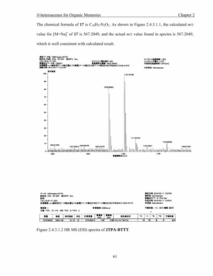
N-heteroacenes for Organic Memories Chapter 2
61
The chemical formula of 17 is C38H27N2O2. As shown in Figure 2.4.3.1.1, the calculated m/z
value for [M+Na]+ of 17 is 567.2049, and the actual m/z value found in spectra is 567.2049,
which is well consistent with calculated result.
Figure 2.4.3.1.2 HR MS (ESI) spectra of 2TPA-BTTT.

N-heteroacenes for Organic Memories Chapter 2
62
The chemical formula of 2TPA-BTTT is C72H73N6Si2. As shown in Figure 2.4.3.1.2, the
calculated m/z value for [M+1]+ of 2TPA-BTTT is 1079.5596, and the actual m/z value of
that found in spectra is 1079.5602, which is well consistent with calculated result.
2.4.3.2 NMR Analysis
1H NMR and 13C NMR spectra of 17 were recorded on a Bruker 300-MHz spectrometer in
CDCl3.
Figure 2.4.3.2.1 1H NMR spectra of 17 in CDCl3.
Figure 2.4.3.2.1 shows the 1H NMR spectra of 17 in CDCl3, the protons can be indexed as 1H
NMR (300 MHz, CDCl3, 298 K): δH = 6.91~6.98 (4H), 7.11~7.20 (12H), 7.28~7.38 (8H),
7.73~7.81 (4H), which are well consistent with its molecular structure.

N-heteroacenes for Organic Memories Chapter 2
63
Figure 2.4.3.2.2 13C NMR spectra of 17 in CDCl3.
Figure 2.4.3.2.2 shows the 13C NMR spectra of 17 in CDCl3. The carbons can be indexed as
13C NMR (101 MHz, CDCl3, 298 K): δC = 193.33, 153.45, 146.01, 131.65, 129.75, 126.42,
125.44, 125.27, 119.04. There are 9 carbons can be observed in the range of 100–200 ppm,
which is well consistent with the theoretical value.
1H NMR and 13C NMR spectra of 2TPA-BTTT were recorded on a JEOL JNM-AL 400-
MHz spectrometer in CD2Cl2.

N-heteroacenes for Organic Memories Chapter 2
64
Figure 2.4.3.2.3 1H NMR spectra of 2TPA-BTTT in CD2Cl2.
Figure 2.4.3.2.3 shows the 1H NMR spectra of 2TPA-BTTT in CD2Cl2, the protons can be
indexed as 1H NMR (400 MHz, CD2Cl2, 298 K): δH = 1.28~1.32 (42H), 6.99~7.04 (4H),
7.10~7.20 (12H), 7.29~7.36 (8H), 7.74~7.80 (4H), 7.85~7.92 (2H), 8.20~8.27 (2H), which
are well consistent with its molecular structure.
Figure 2.4.3.2.4 shows the 13C NMR spectra of 2TPA-BTTT in CD2Cl2. The carbons can be
indexed as 13C NMR (101 MHz, CD2Cl2, 298 K): δC = 155.11, 150.33, 147.55, 145.09,
143.63, 142.08, 132.13, 132.01, 130.67, 129.98, 125.95, 124.50, 121.66, 121.46, 109.80,
102.87, 19.25, 12.23. The carbons located at 12.23 and 19.25 are corresponded to TIPS
group, There are 16 carbons can be observed in range of 100–160 ppm, which is well
consistent with the theoretical value.
N
N
N
N
N
N
Sii-Pr3
Sii-Pr3
2TPA-BTTT
ab
cd
e e
f fg

N-heteroacenes for Organic Memories Chapter 2
65
Figure 2.4.3.2.4 13C NMR spectra of 2TPA-BTTT in CD2Cl2.
2.4.3.3 Crystal Analysis
Needle-like single crystals of 2TPA-BTTT were obtained through slowly diffusion of
CH3CN to its toluene solution. Single-crystal XRD data were collected at 90 K with a
BRUKER-APEX II X-ray diffractometer, which used a large area CCD detector equipped
with graphite monochromated Mo-K alpha radiation (λ = 0.71069 Å). The structures were
solved and refined by SHELXL-97 program. The hydrogen atoms were located at
geometrically calculated positions and were not refined, which were omitted for illustration
convenience. The CCDC number for 2TPA-BTTT is 1014927. Figure 2.4.3.3.1 a) & b)
display the top and side view of 2TPA-BTTT crystal structure. It is clear that TPA unit has a
twisted conformation from both top and side view, which probably induces a bit of bending

N-heteroacenes for Organic Memories Chapter 2
66
Figure 2.4.3.3.1 a) Top view & b) side view of the crystal structure of 2TPA-BTTT. c)
Molecular stacking of 2TPA-BTTT.
in BTTT moiety. As illustrated in Figure 2.4.3.3.1 c), 2D offset intersection face-to-face
stacking mode is adopted between the neighboring molecules of 2TPA-BTTT crystal. The
interlayer distance between BTTT moieties is 3.626 Å, which is larger than that of common
plane N-heteroacenes but shorter than van der Waals bond, indicating that there is strong π-π
interactions between adjacent molecules.

N-heteroacenes for Organic Memories Chapter 2
67
2.4.3.4 Optical Properties of 2TPA-BTTT
Figure 2.4.3.4.1 Normalized UV-vis absorption spectra of 2TPA-BTTT (magenta line: in
solution, violet line: in film).
The investigation of optical properties of 2TPA-BTTT was carried out on a Shimadzu UV-
2501 spectrophotometer through UV-vis absorption spectra. Figure 2.4.3.4.1 shows the
normalized UV-vis absorption spectra of 2TPA-BTTT in CH2Cl2 (magenta line) and in film
(violet line). 2TPA-BTTT exhibits two absorption bands in CH2Cl2 with the maximum
absorption wavelength (λmax) at 548 nm and 594 nm in visible region, respectively. The onset
absorption wavelength (λonset) of 2TPA-BTTT in CH2Cl2 is 709 nm, which determines the
optical band gap (Eg) to be 1.75 eV, based on the same equation illustrated in 2.2.3.4 Optical
Properties of TPA-BIP. The λmax at 548 nm and 594 nm are red-shifted to 607 nm and 658
nm in film, respectively, suggesting the strong π-π interaction between adjacent molecules.
The λonset has a minor red-shift from 709 nm to 721 nm in film as well, corresponding to the
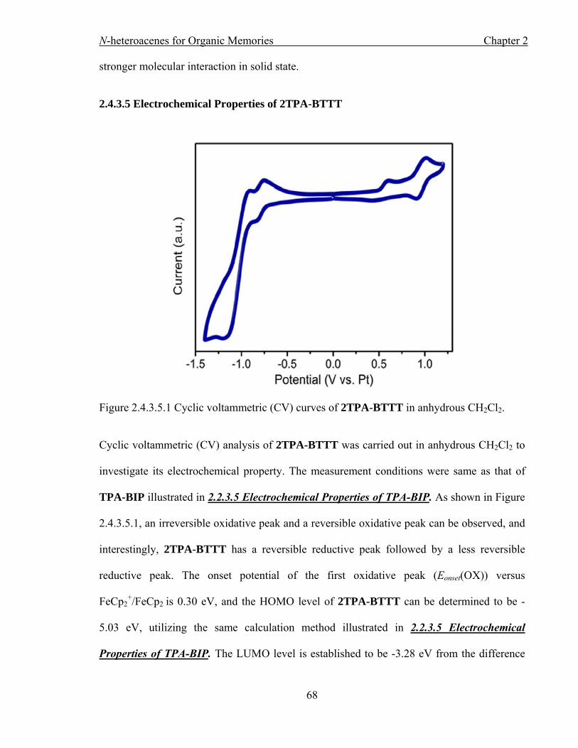
N-heteroacenes for Organic Memories Chapter 2
68
stronger molecular interaction in solid state.
2.4.3.5 Electrochemical Properties of 2TPA-BTTT
Figure 2.4.3.5.1 Cyclic voltammetric (CV) curves of 2TPA-BTTT in anhydrous CH2Cl2.
Cyclic voltammetric (CV) analysis of 2TPA-BTTT was carried out in anhydrous CH2Cl2 to
investigate its electrochemical property. The measurement conditions were same as that of
TPA-BIP illustrated in 2.2.3.5 Electrochemical Properties of TPA-BIP. As shown in Figure
2.4.3.5.1, an irreversible oxidative peak and a reversible oxidative peak can be observed, and
interestingly, 2TPA-BTTT has a reversible reductive peak followed by a less reversible
reductive peak. The onset potential of the first oxidative peak (Eonset(OX)) versus
FeCp2+/FeCp2 is 0.30 eV, and the HOMO level of 2TPA-BTTT can be determined to be -
5.03 eV, utilizing the same calculation method illustrated in 2.2.3.5 Electrochemical
Properties of TPA-BIP. The LUMO level is established to be -3.28 eV from the difference
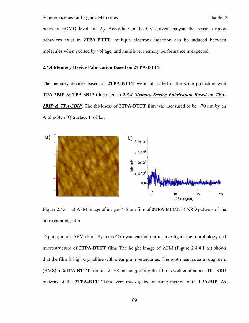
N-heteroacenes for Organic Memories Chapter 2
69
between HOMO level and Eg. According to the CV curves analysis that various redox
behaviors exist in 2TPA-BTTT, multiple electrons injection can be induced between
molecules when excited by voltage, and multilevel memory performance is expected.
2.4.4 Memory Device Fabrication Based on 2TPA-BTTT
The memory devices based on 2TPA-BTTT were fabricated in the same procedure with
TPA-2BIP & TPA-3BIP illustrated in 2.3.4 Memory Device Fabrication Based on TPA-
2BIP & TPA-3BIP. The thickness of 2TPA-BTTT film was measured to be ~70 nm by an
Alpha-Step IQ Surface Profiler.
Figure 2.4.4.1 a) AFM image of a 5 μm × 5 μm film of 2TPA-BTTT. b) XRD patterns of the
corresponding film.
Tapping-mode AFM (Park Systems Co.) was carried out to investigate the morphology and
microstructure of 2TPA-BTTT film. The height image of AFM (Figure 2.4.4.1 a)) shows
that the film is high crystalline with clear grain boundaries. The root-mean-square roughness
(RMS) of 2TPA-BTTT film is 12.168 nm, suggesting the film is well continuous. The XRD
patterns of the 2TPA-BTTT film were investigated in same method with TPA-BIP. As

N-heteroacenes for Organic Memories Chapter 2
70
shown in Figure 2.4.4.1 b), however, only a broad diffraction peak in rang of 4°–7° with low
intensity can be observed. The film might be too thin for XRD diffraction measurement.
2.4.5 Memory Characteristics of 2TPA-BTTT
The memory properties of ITO/2TPA-BTTT/Au devices were demonstrated by current-
voltage (I-V) characteristics, which were measured under same conditions with that of TPA-
BIP Illustrated in 2.2.5 Memory Characteristics of TPA-BIP. The I-V curves are shown in
Figure 2.4.5.1 a). The current of ITO/2TPA-BTTT/Au device retains in low
Figure 2.4.5.1 a) I-V curves, b) resistance distribution & c) retention performance of
ITO/2TPA-BTTT/Au device.

N-heteroacenes for Organic Memories Chapter 2
71
magnitude range in the low sweeping voltage of “Sweep 1”, whose state can be defined as
high resistance state (HRs). There is an abrupt increase of current when the sweeping voltage
approaches the threshold voltage (VTH), indicating the device is switched to low resistance
state (LRs2). The switching process from HRs to LRs2 can be regarded as “SET 1” action.
The LRs2 can be well maintained in the dual sweep or even after removal of the power
supply, suggesting the ITO/2TPA-BTTT/Au device is a typical non-volatile memory. The
current drops into an intermediate range in the reverse “Sweep 2” from 0 V to -1.0 V, in
which state it can be defined as “LRs1”, and the process can be regarded as “RESET 1”
action. The device can be further switched to LRs2 from LRs1 in another positive sweep
(Sweep 3), in which situation the switching acts as “SET 2” process. The initial HRs can be
totally recovered by a large reverse sweep (Sweep 4) from 0 V to -3 V, and the recovery of
from LRs2 to HRs can act as “RESET 2” process. Basically, LRs2 can be generated either
from HRs or LRs1 by “SET 1” or “SET 2” processes, and the “RESET 1” operation is able to
induce the intermediate LRs1 from LRs2. Using a large reverse sweep by “RESET 2”
process HRs can be easily obtained, hence the three distinct resistance states can be well
transformed between each other through “SET 1”, “SET 2” or “RESET 1”, “RESET 2”
operation. On the basis of above analysis, the ITO/2TPA-BTTT/Au device is a rewritable
multilevel memory
The endurance performance of the ITO/2TPA-BTTT/Au devices were investigated with
cyclic switching operations through the typical cycle of “SET 1”-“RESET 1”-“SET 2”-
“RESET 2”. Generally, the device can be repeatedly switched among HRs, LRs1 and LRs2
for more than 70 cycles. Figure 2.4.5.1 3 b) shows the resistances distribution of the three
states for 76 cycles when the device is read at 0.2 V in each state. The average ON/OFF ratio

N-heteroacenes for Organic Memories Chapter 2
72
between “LRs2” and “LRs1” or “LRs1” and “HRs” is ~ 8. The average VTH for LRs2 in
“SET 1” or “SET 2” process is ~1 V, and that for LRs1 in “RESET 1” process is ~(-0.8) V.
The recovery of initial HRs is a gradually changing process, thus the average VTH for HRs in
“RESET 2” process can not be clearly defined. The resistances of the three states distribute in
a narrow magnitude range, suggesting that the multilevel memory behaviors are highly
reproducible.
The retention performance of ITO/2TPA-BTTT/Au devices was evaluated by applying a
reading voltage of -0.2 V to HRs, LRs1 or LRs2 in ambient conditions, respectively. As
shown in Figure 2.4.5.1 3 b), there is no obvious current decay for each state can be observed
in 104 seconds during the test, suggesting that the each memory state is well retentive.
2.4.6 Mechanism Discussion
Molecular calculation based on 2TPA-BTTT was carried out in same method with TPA-BIP
illustrated in 2.2.6 Mechanism Discussion to investigate the switching mechanism and
charge carriers’ migration. As shown in Figure 2.4.6.1 a), the HOMO and LUMO
coefficients of 2TPA-BTTT are distinctly located at TPA and BTTT moieties, respectively.
The distinct distribution of energy levels and the good stacking of 2TPA-BTTT molecules
are favored for intermolecular charge transfer. Figure 2.4.6.1 b) shows the energy diagrams
of ITO/2TPA-BTTT/Au device. The energy barrier between the HOMO of 2TPA-BTTT
and the working function of ITO (-4.8 eV) is determined to be 0.3 eV, however, that between
the LUMO level and the working function of Au (-5.1 eV) is 1.72 eV. Thus, holes injection is
dominated in charge carriers’ migration. It is noteworthy that 2TPA-BTTT has very close
HOMO and HOMO-1 (-5.093 eV) levels based on calculation, so that in a single excitation

N-heteroacenes for Organic Memories Chapter 2
73
Figure 2.4.6.1 a) Electron density distribution of 2TPA-BTTT. b) Energy diagrams of
ITO/2TPA-BTTT/Au system. c) Proposed mechanisms for the multilevel memory behavior.
process double-electron injection might occur. As shown in Figure 2.4.6.1 c), in HRs the
holes injection is possibly blocked by energy barriers between electrodes and organic films,
N-heteroacenes for Organic Memories Chapter 2
74
thus the current of device is under low magnitude range. Double-electron excitation from
HOMO and HOMO-1 levels could occur in “SET 1” process as the voltage approaches to
VTH,8,31 in which situation the device is set to LRs2. The charge transfer complexes can be
formed in this process as main charge carriers, and it should be stable enough even without
electronic field apply, which attributes the non-volatile property of ITO/2TPA-BTTT/Au
device. The charge transfer complexes are possibly partially recombined in the reverse
“RESET 1” process, and the device is reset to LRs1. Applying positive voltage to the
intermediate LRs1 can further realize double-electron excitation again, and accordingly the
LRs2 is achieved from LRs1. A larger reverse sweep can totally release the charge transfer
complex, in which case the initial HRs is recovered.
2.4.7 Summary
In summary, a novel D-A molecule 2TPA-BTTT combining two TPA donor units and one
strong electron-deficient tetraazatetracene acceptor moiety has been designed and
synthesized. The MIM architecture memory devices based on 2TPA-BTTT display non-
volatile rewritable multilevel memory behaviors with good endurance performance. The
charming memory properties are probably generated by multiple electrons intermolecular
charge transfer. This success suggests that incorporating multiple donors with strong
electron-deficient acceptors is an efficient molecules designing strategy to develop novel
rewritable multilevel memory materials.
2.5 References
1 Chen, Y. Zhang, B. Liu, G. Zhuang, X. & Kang, E.-T. Chemical Society Reviews 41,
4688-4707, (2012).

N-heteroacenes for Organic Memories Chapter 2
75
2 Lee, W.-Y. Kurosawa, T. Lin, S. T. Higashihara, T. Ueda, M. & Chen, W.-Z.
Chemistry of Materials 23, 4487-4497, (2011).
3 Wang, K.-L. Liu, Y.-L. Lee, J.-W. Neoh, K.-G. & Kang, E.-T. Macromolecules 43,
7159-7164, (2010).
4 Fang, Y.-K. Liu, C.-L. Li, C. X. Lin, C.-J. Mezzenga, R. & Chen, W.-Z. Advanced
Functional Materials 20, 3012-3024, (2010).
5 Ling, Q. D. Liaw, D.-J. Zhu, C. Chan, D. S.-H, Kang, E.-T. & Neoh, K.-G. Progress
in Polymer Science 33, 917-978, (2008).
6 Liu, Y.-L. Wang, K.-L. Huang, G.-S. Zhu, C.-X. Tok, E.-S. Neoh, K.-G. & Kang, E.-
T. Chemistry of Materials 21, 3391-3399, (2009).
7 Ling, Q. D. Song, Y. Lim, S.-L. Teo, E. Y.-H. Tan, Y.-P. Zhu, C. X. Chan, D. S.-H.
Kwong, D.-L. Neoh, K.-G. & Kang, E.-T. Angewandte Chemie-International Edition
45, 2947-2951, (2006).
8 Ling, Q. D. Chang, F. C. Song, Y. Zhu, C. X. Liaw, D.-J. Chan, D. S.-H. Kang, E.-T.
& Neoh, K.-G. Journal of the American Chemical Society 128, 8732-8733, (2006).
9 Chu, C. W. Ouyang, J. Tseng, H. H. & Yang, Y. Advanced Materials 17, 1440-1443,
200500225 (2005).
10 Ma, L. P. Liu, J. & Yang, Y. Applied Physics Letters 80, 2997-2999, (2002).
11 Hu, B. L. Zhu, X. J. Chen, X. X. Pan, L. Peng, S. S. Wu, Y. Z. Shang, J. Liu, G. Yan,
Q. & Li, R.-W. Journal of the American Chemical Society 134, 17408-17411, (2012).

N-heteroacenes for Organic Memories Chapter 2
76
12 Hu, B. Wang, C. Wang, J. Gao, J. Wang, K. Wu, J. Zhang, G. Cheng, W.
Venkatesvarlu, B. Wang, M. Lee, P. S. & Zhang, Q. Chemical Science 5, 3404-3408,
(2014).
13 Bozano, L. D. Kean, B. W. Beinhoff, M. Carter, K. R. Rice, P. M. & Scott, J. C.
Advanced Functional Materials 15, 1933-1939, (2005).
14 Shang, Y. L. Wen, Y. Q. Li, S. L. Du, S. X. He, X. B. Cai, L. Li, Y. F. Yang, L. M.
Gao, H. J. & Song, Y. L. Journal of the American Chemical Society 129, 11674-
11675, (2007).
15 Jiang, G. Y. Song, Y. L. Guo, X. F. Zhang, D. Q. & Zhu, D. B. Advanced Materials
20, 2888-2898, (2008).
16 Li, H. Xu, Q. Li, N. Sun, R. Ge, J. Lu, J. Gu, H. & Yan, F. Journal of the American
Chemical Society 132, 5542-5543, (2010).
17 Miao, S. F. Li, H. Xu, Q. F. Li, Y. Y. Ji, S. J. Li, N. J. Wang, L. H. Zheng, J. W. & Lu,
J. M. Advanced Materials 24, 6210-6215, (2012).
18 Ye, C. Q. Peng, Q. Li, M. Z. Luo, J. Tang, Z. M. Pei, J. Chen, J. M. Shuai, Z. G. Jiang,
L. & Song, Y. L. Journal of the American Chemical Society 134, 20053-20059,
(2012).
19 Gu, P.-Y. Gao, J. Lu, C.-J. Chen, W. Wang, C. Li, G. Zhou, F. Xu, Q.-F. Lu, J.-M. &
Zhang, Q. Materials Horizons 1, 446-451, (2014).

N-heteroacenes for Organic Memories Chapter 2
77
20 Gu, P. Y. Zhou, F. Gao, J. Li, G. Wang, C. Xu, Q. F. Zhang, Q. & Lu, J. M. Journal
of the American Chemical Society 135, 14086-14089, (2013).
21 Anthony, J. E. Eaton, D. L. & Parkin, S. R. Organic Letters 4, 15-18, (2002).
22 Lindner, B. D. Engelhart, J. U. Tverskoy, O. Appleton, A. L. Rominger, F. Peters, D.-
C. A. Himmel, H.-J. & Bunz. U. H. F. Angewandte Chemie-International Edition 50,
8588-8591, (2011).
23 Bredas, J. L. Silbey, R. Boudreaux, D. S. & Chance, R. R. Journal of the American
Chemical Society 105, 6555-6559, (1983).
24 Colle, M. Buchel, M. & de Leeuw, D. M. Organic Electronics 7, 305-312, (2006).
25 Karthauser, S. Lussem, B. Weides, M. Alba, M. Besmehn, A. OligsChlaeger, R. &
Waser, R. Journal of Applied Physics 100, (2006).
26 Becke, A. D. Journal of Chemical Physics 98, 5648-5652, (1993).
27 Lee, C. T. Yang, W. T. & Parr, R. G. Physical Review B 37, 785-789, (1988).
28 Thompson, A. L. Ahn, T.-S. Thomas, K. R. J. Thayumanavan, S. Martinez, T. J. &
Bardeen, C. J. Journal of the American Chemical Society 127, 16348-16349, (2005).
29 Jia, C. Y. Liu, S.-X. Tanner, C. Leiggener, C. Neels, A. Sanguinet, L. Levillain, E.
Leutwyler , S. Hauser, A. & Decurtins, S. Chemistry-a European Journal 13, 3804-
3812, (2007).

N-heteroacenes for Organic Memories Chapter 2
78
30 Gudeika, D. Michaleviciute, A. Grazulevicius, J. V. Lygaitis, R. Grigalevicius, S.
Jankauskas, V. Miasojedovas, A. Jursenas, S. & Sini, G. The Journal of Physical
Chemistry C 116, 14811-14819, (2012).
31 Freilich, S. C. Macromolecules 20, 973-978, (1987).

N-heteroacenes for Organic Photovoltaics Chapter 3
79
Chapter 3
N-heteroacenes for Organic Photovoltaics
3.1 Literature Review
There has been an intense of research interested in developing novel p-type organic small
molecule semiconducting materials for application in bulk heterojunction (BHJ) architecture
OPVs during the last decade, e.g. subphthalocyanine, merocyanine, squaraine,
diketopyrrolopyrroles, borondipyrromethene, isoindigo, fused acenes, oligothiophenes,
triphenylamine derivatives and so on.1-6 In this part, some representative high performance
small molecules featuring certain designing rules will be reviewed. The chemical structures
of these molecules are shown in Figure 3.1.1.
The early small molecule based BHJ OPVs only showed PCEs in range of 1–3%, whose
efficiency was limited by the low photocurrent density and fill factor.7 A remarkable
breakthrough was achieved by Nguyen’s group in 2009, who developed the small molecule 1
(Figure 3.1.1) with fused benzofuran (BF) as donor and diketopyrrolopyrrole (DPP) as
acceptor, and thiophenes linked the donors and acceptor as a π-bridge.8 The whole molecule
showed a typical D-π-A-π-D structure. The blended film of 1 with [6,6]-phenyl-C71-butyric
acid methyl ester (PC71BM) showed very little phase separation in room temperature.
Interestingly, after thermal annealing, enhanced phase separation of the film could be
achieved and the optimized device showed a PCE up to 4.4% with a Jsc of 10 mA/cm2, a Voc
of 0.9 V, and a FF of 0.48. Inspired by this success, developing novel p-type small molecules
had been speed up. In 2010, Reynolds et al. reported the synthesis of the isoindigo-based

N-heteroacenes for Organic Photovoltaics Chapter 3
80
Figure 3.1.1 Molecular structures of some representative p-type small molecules.
oligoacenes 2 with two oligothiophenes in the end of molecules to play as donors and
isoindigo centered in the middle for acceptor. Employing it as new electron donor and [6,6]-

N-heteroacenes for Organic Photovoltaics Chapter 3
81
phenyl-C61-butyric acid methyl ester (PC61BM) as an acceptor in blended film,9 the as-
fabricated OPV device had a PCE up to 1.76% with a Jsc of 6.3 mA/cm2, a Voc of 0.74 V, and
FF of 0.38. Soon after, the PCE could be further optimized to be 2.15% by using
polydimethylsiloxane (PDMS) as a macromolecular additive.10
An important family of high performance small molecules 3–4 with D-A-D-A-D structure
(Figure 3.1.1) were reported by Bazan and Heeger et al., among them dithieno(3,2-b; 2’,3’-
d)silole (DTS) was used as donor and located in the center. In the famous molecule 3 two
strong electron withdrawing [1,2,5]thiadiazolo[3,4-c]pyridine (PT) groups were used as
acceptors and the ending groups were two bithiophenes.11 Strong and wide absorption of 3 in
visible region was achieved and the molecule owned high hole mobility up to ~0.1 cm2 V-1 s-
1. The OPV device with 3 and PC71BM blended film as active layer showed a PCE up to
6.7%, which was the highest record at that time. It was noteworthy that after adding certain
solvent additive such as 1,8-diiodooctane (DIO) for solution-processing, more excellent OPV
performance could be received. The morphology analysis of the as-prepared film suggested
that the addition of DIO could efficiently decrease the domain sizes. A systematic study on
this family of small molecules had been conducted by Bazan’s group. Deduced from their
research, the OPV performance of these molecules could be significantly influenced by
many factors such as the molecular shape, the bending angle of different unit, and the dipole
moment of molecules.12 Molecule 4 was developed by Gupta and Heeger et al., which used
fluorinated 2,1,3-benzothiadiazole (BT) unit instead of PT as acceptor. The authors believed
that the stronger acceptor moiety could lower the HOMO level of molecules and thus the Voc
of OPV devices would be increased.13 The optimized OPV devices based on 4 utilized an
inverted device structure with polyethylenimine (80% ethoxylated) (PEIE) modified ZnO as

N-heteroacenes for Organic Photovoltaics Chapter 3
82
electron transporting layer, which showed excellent performance with a PCE up to 7.88%
and a Jsc of 15.2 mA/cm2, a Voc of 0.77 V and a FF of 0.67. It was mentionable that high
device stability was observed when the OPVs based on 4 were exposed to ambient conditions.
A family of oligothiophenes based compounds 5a–c, 6 had been designed and synthesized by
Chen and coworkers. For these molecules the single bond linked oligothiophenes were
believed to act as donor moieties and the electron withdrawing groups of alkyl cyanoacetate
were used as acceptors at the ending of molecules.14 Molecule 5b owned a narrow band gap
of 1.8 eV and exhibited the best OPV performance with a PCE up to 5. 08%, and a Jsc of 10.7
mA/cm2, a Voc of 0.86 V, and a FF of 0.55.14 A remarkable advance had been achieved in
recently when the alkyl cyanoacetate groups were changed to 2-(1,1-
dicyanomethylene)rhodanine to produce compound 6, which significantly decreased the
optical band gap to 1.62 eV, mainly coming from the deeper LUMO level of -3.36 eV.15 The
optimized PCE was up to 9.30% (certified at 8.995%) with a Jsc of 14.87 mA/cm2, a Voc of
0.91 V, and a FF of 0.69. The electron transport layer (ETL) materials played a key role for
the enhancement of performance. When poly[(9,9-bis(3′-(N,N-dimethylamino)propyl)-2,7-
fluorene)-alt-2,7-(9,9-dioctylfluorene)] (PFN) was used as ETL material, the devices had
higher and more reproducible performance and the average PCE was 9.03%. When LiF or
ZnO was used as ETL, the average PCE was only 7.55%. The reduced energy barrier
between the electrodes and organic films possibly resulted in the enhancement of devices, in
which case the efficiency of charge carriers transport and collection could be improved
accordingly.
Benzo[1,2-b:4,5-b′]dithiophene (BDT) based small molecules had also been investigated to
be an important family of high performance OPV materials. Li’s group developed a series of

N-heteroacenes for Organic Photovoltaics Chapter 3
83
BDT based small molecules 7–8 with indenedione (ID) as acceptor unit and ending groups.
In these molecules a single thiophene or bithiophene was used as π-bridges, and the authors
believed that the length of π-bridges could influence their OPV performance. Both 7 and 8
had broad absorption in visible region, and the absorption of 8 was significantly enhanced in
comparison with that of 7. The OPV devices based on 8 and PC71BM blended film as active
layer achieved the best performance with a PCE up to 6.75%, a Jsc of 11.05 mA/cm2, a Voc of
0.92 V, and a FF of 66.4%. Chen’s group had also designed a series of BDT based molecules
9–10, 11a–d. Oligothiophenes were used as π-bridges to link the BDT units with various
acceptor moieties, which were alkyl cyanoacetate and 3-ethylrhodanine groups,
respectively.16-18 Different alkyl side chains were attached to the BDT units or acceptor
moieties to investigate their influence on morphology and microstructure of films and OPV
performance. Among these molecules, compound 11b achieved the best OPV performance
when using PDMS as solvent additive, with the optimized parameters of PCE up to 8.12%, a
Jsc of 13.17 mA/cm2, a Voc of 0.93 V, and a FF of 0.66. The authors proposed that the
narrower optical band gap and deeper HOMO levels of molecules could be accounting for
their better device performance. In addition, the morphologies of organic films should also
have certain influence on their OPV performance.
To summarize, the organic small molecules based OPVs have made great progress, and more
exciting discoveries and achievement are expected in the very near future.
3.2 D-π-A Small Molecule with N-heteroacene as Acceptor
3.2.1 Molecular Design
BDT has been widely investigated as excellent donor unit for high performance OPV
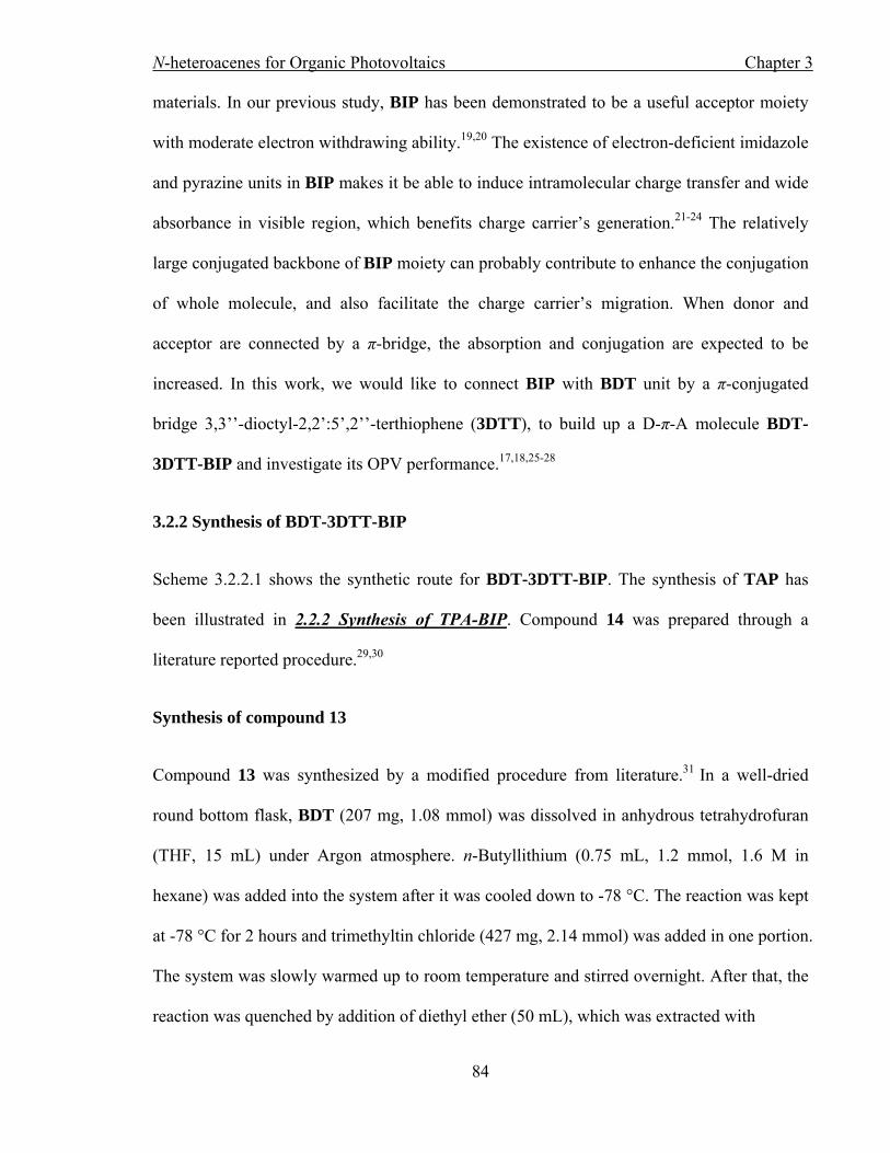
N-heteroacenes for Organic Photovoltaics Chapter 3
84
materials. In our previous study, BIP has been demonstrated to be a useful acceptor moiety
with moderate electron withdrawing ability.19,20 The existence of electron-deficient imidazole
and pyrazine units in BIP makes it be able to induce intramolecular charge transfer and wide
absorbance in visible region, which benefits charge carrier’s generation.21-24 The relatively
large conjugated backbone of BIP moiety can probably contribute to enhance the conjugation
of whole molecule, and also facilitate the charge carrier’s migration. When donor and
acceptor are connected by a π-bridge, the absorption and conjugation are expected to be
increased. In this work, we would like to connect BIP with BDT unit by a π-conjugated
bridge 3,3’’-dioctyl-2,2’:5’,2’’-terthiophene (3DTT), to build up a D-π-A molecule BDT-
3DTT-BIP and investigate its OPV performance.17,18,25-28
3.2.2 Synthesis of BDT-3DTT-BIP
Scheme 3.2.2.1 shows the synthetic route for BDT-3DTT-BIP. The synthesis of TAP has
been illustrated in 2.2.2 Synthesis of TPA-BIP. Compound 14 was prepared through a
literature reported procedure.29,30
Synthesis of compound 13
Compound 13 was synthesized by a modified procedure from literature.31 In a well-dried
round bottom flask, BDT (207 mg, 1.08 mmol) was dissolved in anhydrous tetrahydrofuran
(THF, 15 mL) under Argon atmosphere. n-Butyllithium (0.75 mL, 1.2 mmol, 1.6 M in
hexane) was added into the system after it was cooled down to -78 °C. The reaction was kept
at -78 °C for 2 hours and trimethyltin chloride (427 mg, 2.14 mmol) was added in one portion.
The system was slowly warmed up to room temperature and stirred overnight. After that, the
reaction was quenched by addition of diethyl ether (50 mL), which was extracted with

N-heteroacenes for Organic Photovoltaics Chapter 3
85
Scheme 3.2.2.1 Synthetic route for BDT-3DTT-BIP.
Na2CO3 solution and water. The organic layer was collected and crude product could be
obtained by evaporating solvents. The pure produce was afforded as white powder (252 mg)
by recrystallization of crude products from CH3CN solution in yield of 65.9%.
Synthesis of compound 15
In a well-dried flask, compound 13 (167 mg, 0.47 mmol) and compound 14 (351 mg, 0.59
mmol) were dissolved in anhydrous toluene (20 mL) under Argon atmosphere.
Tetrakis(triphenylphosphine)palladium(0) (59 mg, 0.05 mmol) was added as solid, and the
resulting solution was heated to reflux for 12 hours. After that the system was cooled down to
room temperature, and crude product was obtained by evaporating solvents. The pure

N-heteroacenes for Organic Photovoltaics Chapter 3
86
compound 15 was afforded as orange colour powder (137 mg) by flash column
chromatography over silica get with CH2Cl2 and hexane (CH2Cl2: hexane = 1: 4) in yield of
42.3%.
Synthesis of BDT-3DTT-BIP
In a round bottom flask, TAP (159 mg, 0.28 mmol), compound 15 (165 mg, 0.24 mmol)
were dissolved in N,N-dimethylmethanamide (DMF 25 mL). Sodium metabisulfite (61 mg,
0.32 mmol) was added and the system was heated to 120 °C for 12 hours. After cooled down
to room temperature, the mixture was poured into ice water (100 mL) and filtered, the solid
residue was obtained as crude product, and the pure BDT-3DTT-BIP was afforded as dark
red powder (61 mg) by flash column chromatography over silica gel with CH2Cl2 and hexane
(CH2Cl2: hexane = 1: 3) in a yield of 20.4%.
3.2.3 Molecular Characterization
The compound 13, 15 and BDT-3DTT-BIP have been characterized by HR MS and NMR.
3.2.3.1 HR MS Analysis
The HR MS (MALDI-TOF) spectra of 15 and BDT-3DTT-BIP were recorded on a JEOL
spiral TOF JMS-S3000 spectrometer.
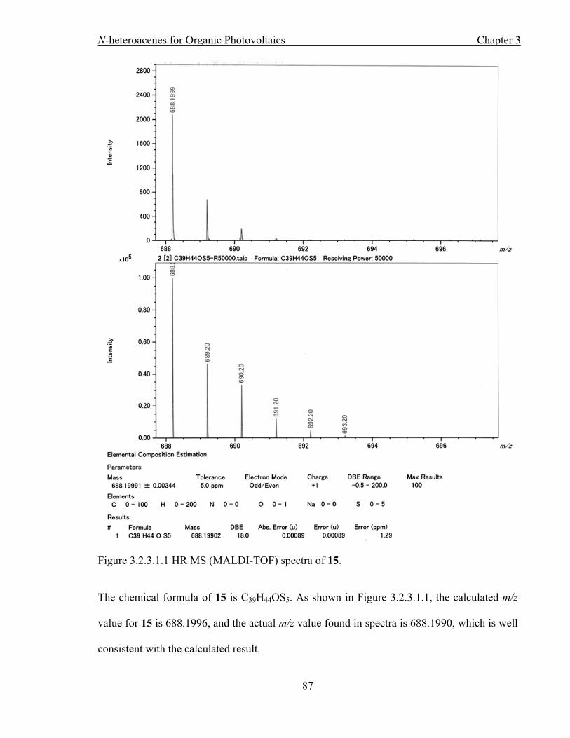
N-heteroacenes for Organic Photovoltaics Chapter 3
87
Figure 3.2.3.1.1 HR MS (MALDI-TOF) spectra of 15.
The chemical formula of 15 is C39H44OS5. As shown in Figure 3.2.3.1.1, the calculated m/z
value for 15 is 688.1996, and the actual m/z value found in spectra is 688.1990, which is well
consistent with the calculated result.

N-heteroacenes for Organic Photovoltaics Chapter 3
88
Figure 3.2.3.1.2 HR MS (MALDI-TOF) spectra of BDT-3DTT-BIP.
The chemical formula of BDT-3DTT-BIP is C73H90N4Si2S5. As shown in Figure 3.2.3.1.2,
the calculated m/z value for [M+1]+ of BDT-3DTT-BIP is 1239.5308, and the actual m/z
value for that found in spectra is 1239.5380, which is well consistent with the calculated
result.

N-heteroacenes for Organic Photovoltaics Chapter 3
89
3.2.3.2 NMR Analysis
1H NMR spectra of 13 was recorded on a JEOL JNM-AL300 spectrometer in CDCl3.
Figure 3.2.3.2.1 1H NMR spectra of 13 in CDCl3.
Figure 3.2.3.2.1 shows the 1H NMR spectra of 13 in CDCl3, the protons can be indexed as 1H
NMR (300 MHz, CDCl3, 298 K): δH = 8.10~8.43 (2H), 7.37~7.51 (2H), 7.37~7.28 (1H),
0.26~0.51 (9H), which are well consistent with its molecular structure.

N-heteroacenes for Organic Photovoltaics Chapter 3
90
Figure 3.2.3.2.2 1H NMR spectra of 15 in CDCl3.
1H NMR and 13C NMR spectra of 15 were recorded on a JEOL JNM-ECX400 spectrometer
in CDCl3.
Figure 3.2.3.2.2 shows the 1H NMR spectra of 15 in CDCl3, the protons can be indexed as 1H
NMR (400 MHz, CDCl3, 298 K): δH = 9.80~9.88 (1H), 8.17~8.25 (2H), 7.56~7.65 (1H),
7.45~7.50 (1H), 7.41~7.45 (1H), 7.32~7.38 (1H) 7.26~7.30 (1H), 7.13~7.19 (2H), 2.74~2.89
(4H), 1.64~1.77 (4H), 1.28~1.48 (20H), 0.82~0.94 (6H), which are well consistent with its
molecular structure.

N-heteroacenes for Organic Photovoltaics Chapter 3
91
Figure 3.2.3.2.3 13C NMR spectra of 15 in CDCl3.
Figure 3.2.3.2.3 shows the 13C NMR spectra of 15. The carbons can be indexed as 13C NMR
(101 MHz, CDCl3, 298 K): δC = 182.56, 141.16, 140.92, 140.42, 140.28, 139.08, 138.10,
137.85, 137.68, 137.60, 137.03, 136.40, 135.72, 134.78, 130.14, 128.30, 127.89, 127.19,
126.37, 123.01, 118.83, 116.68, 116.49, 31.89, 31.87, 30.52, 30.33, 29.62, 29.51, 29.45,
29.42, 29.28, 29.26, 22.68, 14.12. There are 35 carbons can be observed, which is well
consistent with the theoretical value.
N-heteroacenes for Organic Photovoltaics Chapter 3
92
Figure 3.2.3.2.4 1H NMR spectra of BDT-3DTT-BIP in CD2Cl2.
1H NMR and 13C NMR spectra of BDT-3DTT-BIP were recorded on a JEOL JNM-ECX400
spectrometer in CD2Cl2.
Figure 3.2.3.2.4 shows the 1H NMR spectra of BDT-3DTT-BIP in CD2Cl2, the protons can
be indexed as 1H NMR (400 MHz, CD2Cl2, 298 K): δH = 9.51~9.92 (1H), 8.05~8.28 (4H),
7.71~7.82 (2H), 7.61~7.67 (1H), 7.38~7.43 (1H), 7.34~7.34 (1H), 7.23~7.29 (2H), 7.15~7.19
(1H), 7.11~7.15 (1H), 2.69~2.83 (4H), 1.67~1.78 (4H), 1.23~1.46 (62H), 0.84~0.93 (6H),
which are well consistent with its molecular structure.

N-heteroacenes for Organic Photovoltaics Chapter 3
93
Figure 3.2.3.2.4 13C NMR spectra of BDT-3DTT-BIP in CD2Cl2.
Figure 3.2.3.2.3 shows the 13C NMR spectra of BDT-3DTT-BIP in CD2Cl2. The carbons can
be indexed as 13C NMR (101 MHz, CD2Cl2C = 153.41, 142.86, 141.44, 141.26,
138.56, 138.16, 138.07, 137.89, 137.62, 137.47, 136.75, 135.66, 135.17, 133.11, 131.08,
130.45, 129.96, 128.91, 128.45, 127.92, 127.72, 126.64, 123.47, 119.16, 117.12, 116.87,
32.51, 31.03, 30.81, 30.28, 30.25, 30.21, 30.16, 30.10, 30.03, 29.92, 23.29, 23.25, 19.32,
14.48, 14.45, 12.23. There are only 26 carbons can be observed in range of 100–160 ppm,
which is 5 carbons less than theoretical value. Maybe certain carbons of BDT-3DTT-BIP
have no signals in 13C NMR spectra in our experimental conditions.

N-heteroacenes for Organic Photovoltaics Chapter 3
94
3.2.3.3 Optical Properties of BDT-3DTT-BIP
Figure 3.2.3.3.1 Normalized UV-vis absorption spectra of BDT-3DTT-BIP film (magenta),
BDT-3DTT-BIP/PC61BM blended film (navy) & BDT-3DTT-BIP/PC71BM blended film
(violet).
The optical properties of BDT-3DTT-BIP film and its blended films with PC61BM or
PC71BM were investigated by UV-vis absorption spectra recorded on a JASCO UV/VIS/NIR
Spectro-photometer V-670. The normalized absorption spectra are shown in Figure 3.2.3.3.1.
BDT-3DTT-BIP film has two absorption bands in visible region, whose maximum
absorption wavelength (λmax) is at 458 nm and 547 nm, respectively. The onset absorption
wavelength (λonset) is 665 nm, which determines the optical band gap (Eg) of 1.86 eV based
on the equation illustrated in 2.2.3.4 Optical Properties of TPA-BIP. When blended with
PC61BM in 1:1 ratio, the λmax at 547 nm is blue-shifted to 508 nm, meanwhile, the λmax of
BDT-3DTT-BIP/PC71BM blended film in 1:1 ratio also has a blue-shift to 531 nm, which is
still 23 nm red-shifted compared to the BDT-3DTT-BIP/PC61BM blended film. Thus, the

N-heteroacenes for Organic Photovoltaics Chapter 3
95
BDT-3DTT-BIP/PC71BM blended film has a minor wider absorption range and moderate
miscibility. Both the two blended films cover a broad range of absorption in visible region
from 400 nm to 642 nm, suggesting they might have the potential to obtain high Jsc in OPV
devices.
3.2.3.4 Electrochemical Properties of BDT-3DTT-BIP
Table 3.2.3.4.1 Statistic ionization potentials of BDT-3DTT-BIP.
Samples 1 2 3 4 Average
IP (eV) -5.37 -5.38 -5.32 -5.32 -5.35
Ionization potential (IP) was evaluated with atmospheric photoelectron spectroscopy (Riken
Keiki, AC-3) to investigate the electrochemical properties of BDT-3DTT-BIP. Table
3.2.3.4.1 summarizes the statistic IPs, and the average IP is measured to be -5.35 eV, which
establishes the HOMO level of BDT-3DTT-BIP. The LUMO level is determined to be -3.49
eV from the difference between HOMO level and Eg.
3.2.4 OPV Device Fabrication Based on BDT-3DTT-BIP
The OPV devices were fabricated with a typical BHJ architecture of ITO/anode buffer
layer/donor:acceptor/Ca/Al through solution-processing method. Poly(3,4-
ethylenedioxythiophene):poly(styrenesulfonate) (PEDOT:PSS) or molybdenum oxide
(MoO3) was adopted as anode buffer layer, and PC61BM or PC71BM was used as acceptor,
respectively. The ITO glass substrates (20.0 mm × 20.0 mm, 15 Ω per square) were pre-
cleaned by water Semico clean 56, water, and isopropanol under ultrasonic. After dried on a
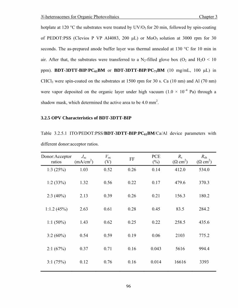
N-heteroacenes for Organic Photovoltaics Chapter 3
96
hotplate at 120 °C the substrates were treated by UV/O3 for 20 min, followed by spin-coating
of PEDOT:PSS (Clevios P VP AI4083, 200 μL) or MoO3 solution at 3000 rpm for 30
seconds. The as-prepared anode buffer layer was thermal annealed at 130 °C for 10 min in
air. After that, the substrates were transferred to a N2-filled glove box (O2 and H2O < 10
ppm). BDT-3DTT-BIP/PC61BM or BDT-3DTT-BIP/PC71BM (10 mg/mL, 100 μL) in
CHCl3 were spin-coated on the substrates at 1500 rpm for 30 s. Ca (10 nm) and Al (70 nm)
were vapor deposited on the organic layer under high vacuum (1.0 × 10⁻⁴ Pa) through a
shadow mask, which determined the active area to be 4.0 mm2.
3.2.5 OPV Characteristics of BDT-3DTT-BIP
Table 3.2.5.1 ITO/PEDOT:PSS/BDT-3DTT-BIP:PC61BM/Ca/Al device parameters with
different donor:acceptor ratios.
Donor:Acceptor ratios
Jsc
(mA/cm2) Voc
(V) FF
PCE (%)
Rs (Ω cm2)
Rsh (Ω cm2)
1:3 (25%) 1.03 0.52 0.26 0.14 412.0 534.0
1:2 (33%) 1.32 0.56 0.22 0.17 479.6 370.3
2:3 (40%) 2.13 0.39 0.26 0.21 156.3 180.2
1:1.2 (45%) 2.63 0.61 0.28 0.45 83.5 284.2
1:1 (50%) 1.43 0.62 0.25 0.22 258.5 435.6
3:2 (60%) 0.54 0.59 0.19 0.06 2103 775.2
2:1 (67%) 0.37 0.71 0.16 0.043 5616 994.4
3:1 (75%) 0.12 0.76 0.16 0.014 16616 3393

N-heteroacenes for Organic Photovoltaics Chapter 3
97
The OPV performance of BDT-3DTT-BIP is demonstrated by current-voltage (J-V) curves,
which were recorded on a Keithley 2611B SYSTEM Source Mater unit under AM 1.5G
illumination at the intensity of 100 mW/cm2 using a solar simulator (Bunko-keiki, CEP-
2000RP). The external quantum efficiency (EQE) was measured under illumination of
monochromatic light using the same system at the intensity of 1.25 mW/cm2.
The optimized weight ratio of BIP-3DTT-BDT to PC61BM or PC71BM was 1: 1.2, the
detailed parameters are summarized in Table 3.2.5.1.
Table 3.2.5.2 ITO/PEDOT:PSS/BDT-3DTT-BIP:PC61BM (1:1.2)/Ca/Al device parameters
at different annealing temperature.
Annealing temperature (oC )
Jsc (mA/cm2)
Voc (V)
FF PCE (%)
Rs (Ω cm2)
Rsh (Ω cm2)
non-annealing 2.63 0.61 0.28 0.45 83.5 284.2
85 2.49 0.57 0.28 0.39 103.5 271.3
100 1.32 0.65 0.21 0.18 668 398.9
120 0.53 0.20 0.25 0.03 390.0 358.2
140 0.29 0.58 0.17 0.03 3270 1173
150 0.13 0.50 0.17 0.01 5788 222.8
Thermal annealing has already been proved to be effective for controlling film morphology
to facilitate charge carrier separation and transportation, while it did not work well to
improve the performance of our devices.32,33 When the ITO/PEDOT:PSS/BDT-3DTT-
BIP:PC61BM/Ca/Al device was thermal treated at 100 oC, the PCE was largely decreased

N-heteroacenes for Organic Photovoltaics Chapter 3
98
from 0.45% to 0.18%, the detailed parameters are summarized in Table 3.2.5.2. To further
investigate the reason why thermal annealing decreased the PCE of devices, we measured the
AFM images of BDT-3DTT-BIP/PC61BM blended film in two conditions: without
annealing and annealed at 100 oC. After annealing, increased domain size in film were
observed, which could decrease the exciton dissociation at the donor:acceptor interfaces due
to the reduced interface area. This phenomenon was consistent with the decreased Jsc of
device after annealed at 100 oC.
Table 3.2.5.3 ITO/PEDOT:PSS/BDT-3DTT-BIP:PC61BM (1:1.2)/Ca/Al device parameters
with different DIO concentration.
DIO concentration (%)
Jsc (mA/cm2 )
Voc
(V) FF
PCE (%)
Rs (Ω cm2)
Rsh
(Ω cm2)
0 2.63 0.61 0.28 0.45 83.5 284.2
0.1 3.18 0.58 0.28 0.51 103.8 233.6
0.2 2.06 0.47 0.31 0.30 72.4 306.9
0.5 4.42 0.57 0.36 0.90 37.2 273.1
1 - - - - - -
1,8-diiodooctane (DIO) was added to the mixed donor:acceptor solutions and might enhance
the crystallization of BDT-3DTT-BIP.34 The PCE of ITO/PEDOT:PSS/BDT-3DTT-
BIP:PC61BM/Ca/Al device with 0.5 % DIO addition by volume was double enhanced from
0.45% to 0.9% compared to the device without DIO addition, the detailed parameters are
summarized in Table 3.2.5.3.
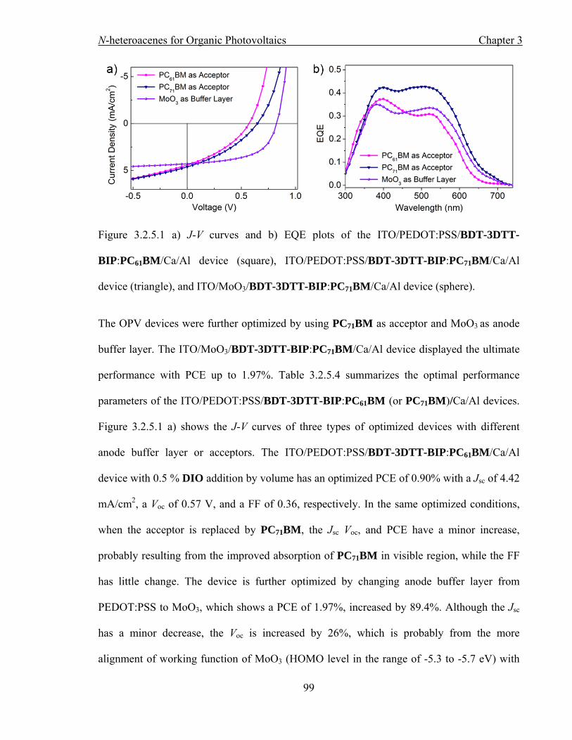
N-heteroacenes for Organic Photovoltaics Chapter 3
99
Figure 3.2.5.1 a) J-V curves and b) EQE plots of the ITO/PEDOT:PSS/BDT-3DTT-
BIP:PC61BM/Ca/Al device (square), ITO/PEDOT:PSS/BDT-3DTT-BIP:PC71BM/Ca/Al
device (triangle), and ITO/MoO3/BDT-3DTT-BIP:PC71BM/Ca/Al device (sphere).
The OPV devices were further optimized by using PC71BM as acceptor and MoO3 as anode
buffer layer. The ITO/MoO3/BDT-3DTT-BIP:PC71BM/Ca/Al device displayed the ultimate
performance with PCE up to 1.97%. Table 3.2.5.4 summarizes the optimal performance
parameters of the ITO/PEDOT:PSS/BDT-3DTT-BIP:PC61BM (or PC71BM)/Ca/Al devices.
Figure 3.2.5.1 a) shows the J-V curves of three types of optimized devices with different
anode buffer layer or acceptors. The ITO/PEDOT:PSS/BDT-3DTT-BIP:PC61BM/Ca/Al
device with 0.5 % DIO addition by volume has an optimized PCE of 0.90% with a Jsc of 4.42
mA/cm2, a Voc of 0.57 V, and a FF of 0.36, respectively. In the same optimized conditions,
when the acceptor is replaced by PC71BM, the Jsc Voc, and PCE have a minor increase,
probably resulting from the improved absorption of PC71BM in visible region, while the FF
has little change. The device is further optimized by changing anode buffer layer from
PEDOT:PSS to MoO3, which shows a PCE of 1.97%, increased by 89.4%. Although the Jsc
has a minor decrease, the Voc is increased by 26%, which is probably from the more
alignment of working function of MoO3 (HOMO level in the range of -5.3 to -5.7 eV) with

N-heteroacenes for Organic Photovoltaics Chapter 3
100
the HOMO level of BDT-3DTT-BIP.35 The FF also has a large increase by 60%. The
enhancement is probably coming from the reduced chemical interaction between BDT-
3DTT-BIP and anode buffer layer, because the N atoms in BIP can react with the acidic
PEDOT:PSS, which thus decreases the OPV performance.35-37
The EQE plots of the as-fabricated devices were investigated and the corresponded plots are
shown in Figure 3.2.5.1 b). ITO/PEDOT:PSS/BDT-3DTT-BIP:PC61BM/Ca/Al device has
high conversion of absorption (EQE > 10%) from 309 nm to 611 nm, with two maximum
EQE value at 396 nm (37%) and 521 nm (31%), respectively. As PC71BM is used as
acceptor, the range of high photon conversion (EQE > 10%) is expanded from 311 nm to 644
nm, which is 31 nm broader than the device with PC61BM as acceptor. The larger photo
conversion range is corresponded to the broader absorption of BDT-3DTT-BIP/PC71BM
blended film and the higher Jsc in J-V curves of ITO/PEDOT:PSS/BDT-3DTT-
BIP:PC71BM/Ca/Al device. The maximum EQE values are increased to 42% at 399 nm and
43% at 508 nm, respectively. Keeping PC71BM as acceptor, when the anode buffer layer is
replaced with MoO3, the EQE curves show similar tendency but with decreased EQE at 35%
(384 nm) and 34% (522 nm), respectively. The higher EQE efficiency of
ITO/PEDOT:PSS/BDT-3DTT-BIP:PC71BM/Ca/Al device probably results from the
existence of leakage current in the dark.

N-heteroacenes for Organic Photovoltaics Chapter 3
101
Table 3.2.5.4 Optimal performance parameters of the ITO/PEDOT:PSS/BDT-3DTT-
BIP:PC61BM (or PC71BM)/Ca/Al devices.
Devices Voc (V)
Jsc (mA/cm2)
FF PCE (%)
PC61BM as acceptora
0.61 2.63 0.28 0.45
PC61BM as acceptorb
0.65 1.32 0.21 0.18
PC61BM as acceptorc
0.57 4.42 0.36 0.90
PC71BM as acceptord
0.65 4.62 0.35 1.04
MoO3 as buffer layere
0.82 4.29 0.56 1.97
aITO/PEDOT:PSS/BDT-3DTT-BIP:PC61BM/Ca/Al device without DIO addition and
thermal annealing.
bITO/PEDOT:PSS/BDT-3DTT-BIP:PC61BM /Ca/Al device without DIO addition and
annealed at 100 oC.
cITO/PEDOT:PSS/BDT-3DTT-BIP:PC61BM /Ca/Al device with 0.5% DIO addition and
without thermal annealing.
dITO/PEDOT:PSS/BDT-3DTT-BIP:PC71BM//Ca/Al device with 0.5% DIO addition and
without thermal annealing.
eITO/PEDOT:PSS/BDT-3DTT-BIP:PC71BM/Ca/Al device with 0.5% DIO addition and
without thermal annealing.

N-heteroacenes for Organic Photovoltaics Chapter 3
102
3.2.6 Results Discussion
3.2.6.1 Molecular Calculation
Figure 3.2.6.1.1 Electron density distribution of HOMO & LUMO levels of BDT-3DTT-BIP.
Molecular calculation was carried out to study the intrinsic molecular configuration and
electron density distribution of BDT-3DTT-BIP in same method with TPA-2BIP & TPA-
3BIP illustrated in 2.3.6 Mechanism Discussion.38,39 As shown in Figure 3.2.6.1.1, the
optimized structure of BDT-3DTT-BIP shows a broad “V” shape conformation, and the two
octyl chains are in the same side. The HOMO coefficient is distributed on the BDT and
3DTTT units, while LUMO coefficient is mainly located on the BIP moiety. The calculated
molecular ground state dipole moment is 4.90 D, which is also consistent with the electron
density distribution of HOMO and LUMO levels. The stronger intramolecular charge transfer
can facilitate the charge separation at the donor:acceptor interfaces, thus improve the OPV
performance.
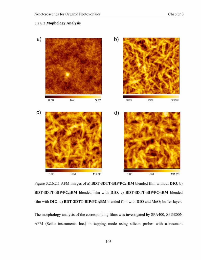
N-heteroacenes for Organic Photovoltaics Chapter 3
103
3.2.6.2 Mophology Analysis
Figure 3.2.6.2.1 AFM images of a) BDT-3DTT-BIP/PC61BM blended film without DIO, b)
BDT-3DTT-BIP/PC61BM blended film with DIO, c) BDT-3DTT-BIP/PC71BM blended
film with DIO, d) BDT-3DTT-BIP/PC71BM blended film with DIO and MoO3 buffer layer.
The morphology analysis of the corresponding films was investigated by SPA400, SPI3800N
AFM (Seiko instruments Inc.) in tapping mode using silicon probes with a resonant

N-heteroacenes for Organic Photovoltaics Chapter 3
104
frequency of ~138 kHz and a force constant of 16 N m-1. As shown in Figure 3.2.6.2.1 a),
when BDT-3DTT-BIP/PC61BM blended film spin-coated on ITO/PEDOT:PSS substrate
without the addition of DIO, the film is smooth and well continuous with a small roughness
(RMS = 0.48 nm). As DIO is added, the film shows a large increase of RMS from 0.48 nm to
15 nm (Figure 3.2.6.2.1 b)). The increased domain size and crystallinity of blended film can
be observed and possibly enhance the charge carrier’s transportation, thus contribute to the
improved Jsc (from 2.63 to 4.42 mA/cm2) and FF (from 28% to 36%). Meanwhile, the BDT-
3DTT-BIP/PC71BM blended films on ITO/PEDOT:PSS or ITO/MoO3 substrate (Figure
3.2.6.2.1 c) & (d)) show similar morphologies with close roughness after adding DIO (RMS
= 18.2 nm and RMS = 20.2 nm, respectively). The performance enhancement of
ITO/MoO3/BDT-3DTT-BIP:PC71BM/Ca/Al device might have little relevance to the
morphology.
3.2.6.3 XRD Patterns Analysis
The out-of-plane XRD patterns of the corresponding films was collected on a RINT-
TTR /NM diffractometer equipped with a rotating anode (Cu Kα radiation, λ = 1.5418 Å). Ⅲ
As shown in Figure 3.2.6.3.1, the BDT-3DTT-BIP/PC61BM blended film shows no
diffraction peak. After adding DIO, a diffraction peak at 2θ = ca. 4.6° can be observed,
which is corresponding to the d100 spacing value (the distance between the planes of the
major conjugated backbone separated by the longer alkyl chain (C8H17) of 19.3 Å.40 The
obvious XRD peak suggests that highly organized assembly of BDT-3DTT-BIP molecules
after adding the DIO. The BDT-3DTT-BIP/PC71BM blended film shows similar diffraction
peak position when DIO is added, but the peak is much sharper than BDT-3DTT-
BIP/PC61BM blended film, suggesting it has higher crystallinity.

N-heteroacenes for Organic Photovoltaics Chapter 3
105
Figure 3.2.6.3.1 XRD patterns of corresponding films (magenta: BDT-3DTT-BIP/PC61BM
blended film without DIO, navy: BDT-3DTT-BIP/PC61BM blended film with DIO, orange:
BDT-3DTT-BIP/PC71BM blended film with DIO on PEDOT:PSS, violet: BDT-3DTT-
BIP/PC71BM blended film with DIO on MoO3).
When anode buffer layer (PEDOT:PSS) is changed to MoO3, a peak in same position can be
observed with a minor decreased sharpness. In previous study, people has already
demonstrated that the donor molecules have stronger nucleation and crystallinity on
PEDOT:PSS surface because of certain interactions, which explains the lower crystallinity of
BDT-3DTT-BIP/PC71BM blended film on MoO3 surface.41 The enhanced PCE probably
N-heteroacenes for Organic Photovoltaics Chapter 3
106
mainly comes from the more aligned energy level and reduced chemical reaction between
active layer and anode buffer layer.
Campared with the highest record in recent advances, there is a gap of efficiency for BDT-
3DTT-BIP with PCE ~2%. From the analysis of AFM images (Figure 3.2.6.2.1), the surface
of the active layer is in high roughness. The rough surface could induce bad contact between
the electrodes and active layer, which was not favor for the transportation and collection of
the separated charge carriers. This result corresponded to the increased intensity of (100)
peak in Figure 3.2.6.3.1, which proved that the crystallinity of BDT-3DTT-BIP was
enhanced after adding DIO. The above discussion might explain the relatively low Jsc and
PCE of BDT-3DTT-BIP based OPV devices, which was mainly ascribed to the excessive
crystalization of BDT-3DTT-BIP.
3.2.7 Summary
In summary, a novel D-π-A small molecule BDT-3DTT-BIP with an N-heteroacene as
acceptor moiety has been synthesized and characterised. The standard BHJ structure OPV
devices are investigated through solution-processing method with different acceptor materials
and different anode buffer layers. The ultimate performance is achieved by using PC71BM as
acceptor and MoO3 as anode buffer layer, the optimised PCE is 1.97%. AFM images and
XRD patterns indicates the anode buffer layer has no obvious influence on film morphologies,
and combining with the J-V curves and EQE plots, the more aligned working function of
anode buffer layer and reduced chemical interactions between buffer layer and active layer
play an important role to enhance the PCE of the devices.

N-heteroacenes for Organic Photovoltaics Chapter 3
107
3.3 References
1 Tang, W. Hai, J, Dai, Y. Huang, Z. Lu, B. Yuan, F. Tang, J. & Zhang, F. Solar
Energy Materials and Solar Cells 94, 1963-1979, (2010).
2 Lin, Y., Li, Y. & Zhan, X. Chemical Society Reviews 41, 4245-4272, (2012).
3 Shen, S. Jiang, P. He, C. Zhang, J. Shen, P. Zhang, Y. Yi, Y. Zhang, Z. Li, Z. & Li, Y.
Chemistry of Materials 25, 2274-2281, (2013).
4 Roncali, J. Accounts of Chemical Research 42, 1719-1730, (2009).
5 Walker, B. Kim, C. & Nguyen, T.-Q. Chemistry of Materials 23, 470-482, (2011).
6 Li, Y., Guo, Q. Li, Z. Pei, J. & Tian, W. Energy & Environmental Science 3, 1427-
1436, (2010).
7 Tang, C. W. Applied Physics Letters 48, 183-185, (1986).
8 Walker, B. Tamayo, A. B. Dang, X.-D. Zalar, P. Seo, J. H. Garcia, A. Tantiwiwat, M.
& Nguyen, T.-Q. Advanced Functional Materials 19, 3063-3069, (2009).
9 Mei, J. Graham, K. R. Stalder, R. & Reynolds, J. R. Organic Letters 12, 660-663,
(2010).
10 Graham, K. R. Wieruszewski, P. M. Stalder, R. Hartel, M. J. Mei, J. So, F. &
Reynolds, J. R. Advanced Functional Materials 22, 4801-4813, (2012).
11 Sun, Y. Welch, G. C. Leong, W. L. Takacs, C. J. Bazan, G. C. & Heeger, A. J. Nature
Materials 11, 44-48, (2012).

N-heteroacenes for Organic Photovoltaics Chapter 3
108
12 Takacs, C. J. Sun, Y. M. Welch, G. C. Perez, L. A. Liu, X. F. Wen, W. Bazan, G. C.
& Heeger, A. J. Journal of the American Chemical Society 134, 16597-16606, (2012).
13 Kyaw, A. K. K. Wang, D. H. Gupta, V. Zhang, J. Chand, S. Bazan, G. C. & Heeger,
A. J. Advanced Materials 25, 2397-2402, (2013).
14 Liu, Y. Wan, X. Wang, F. Zhou, J. Long, G. Tian, J. You, J. Yang, Y. & Chen, Y.
Advanced Energy Materials 1, 771-775, (2011).
15 Zhang, Q. Kan, B. Liu, F. Long, G. Wan, X. Chen, X. Zuo, Y. Ni, W. Zhang, H. Li,
M. Hu, Z. Huang, F. Cao, Y. Liang, Z. Zhang, M. Russell, T. R. & Chen, Y. Nature
Photonics 9, 35-41, (2015).
16 Liu, Y. Wan, X. Wang, F. Zhou, J. Long, G. Tian, J. & Chen, Y. Advanced Materials
23, 5387-5391, (2011).
17 Zhou, J. Wan, X. Liu, Y. Zuo, Y. Li, Z. He, G. Long, G. Ni, W. Li, C. Su, X. & Chen,
Y. Journal of the American Chemical Society 134, 16345-16351, (2012).
18 Zhou, J. Zuo, Y. Wan, X. Long, G. Zhang, Q. Ni, W. Liu, Y. Li, Z. He, G. Li, C. Kan,
B. Li, M. & Chen, Y. Journal of the American Chemical Society 135, 8484-8487,
(2013).
19 Wang, C. Wang, J. Li, P.–Z. Gao, J. Tan, S. Y. Xiong, W.–W. Hu, B. Lee. P. S. Zhao,
Y. & Zhang, Q. Chemistry-an Asian Journal 9, 779-783, (2014).

N-heteroacenes for Organic Photovoltaics Chapter 3
109
20 Wang, C. Hu, B. Wang, J. Gao, J. Li, G. Xiong, W.–W. Zou, B. Suzuki, M. Aratani,
N. Yamada, H. Huo, F. Lee. P. S. & Zhang, Q. Chemistry – An Asian Journal 10,
116-119, (2015).
21 Bunz, U. H. F. Chemistry-a European Journal 15, 6780-6789, (2009).
22 Bunz, U. H. F. Engelhart, J. U. Lindner, B. D. & Schaffroth, M. Angewandte Chemie-
International Edition 52, 3810-3821, (2013).
23 Kivala, M. Pisula, W. Wang, S. Mavrinskiy, A. Gisselbrecht, J.-P. Feng, X. & Müllen,
K. Chemistry-a European Journal 19, 8117-8128, (2013).
24 Schlutter, F. Rossel, F. Kivala, M. Enkelmann, V. Gisselbrecht, J.-P. Ruffieux, P.
Fasel, R. & Müllen, K. Journal of the American Chemical Society 135, 4550-4557,
(2013).
25 Hou, J. Park, M.-H. Zhang, S. Yao, Y. Chen, L.-M. Li, J.-H. & Yang, Y.
Macromolecules 41, 6012-6018, (2008).
26 Wang, M. Hu, X. Liu, P. Li, W. Gong, X. Huang, F. & Cao, Y. Journal of the
American Chemical Society 133, 9638-9641, (2011).
27 Price, S. C. Stuart, A. C. Yang, L. Zhou, H. & You, W. Journal of the American
Chemical Society 133, 4625-4631, (2011).
28 Dou, L. Chang, W.-H. Gao, J. Chen, C.-C. You, J. & Yang, Y. Advanced Materials
25, 825-831, (2013).
29 Meng, H. & Huang, W. Journal of Organic Chemistry 65, 3894-3901, (2000).

N-heteroacenes for Organic Photovoltaics Chapter 3
110
30 Zhou, J. Wan, X. Liu, Y, Long, G, Wang, F. Li, Z. Zuo, Y. Li, C. & Chen, Y.
Chemistry of Materials 23, 4666-4668, (2011).
31 Rieger, R. Beckmann, D. Mavrinskiy, A., Kastler, M. & Müllen, K. Chemistry of
Materials 22, 5314-5318, (2010).
32 Shah, A. Torres, P. Tscharner, R. Wyrsch, N. & Keppner, H. Science 285, 692-698,
(1999).
33 Shang, H. Fan, H. Liu, Y. Hu, W. Li, Y. & Zhan, X. Advanced Materials 23, 1554-
1557, (2011).
34 Peet, J. Kim, J. Y. Coates, N. E. Ma, D. W. Moses, L. Heeger, A. J. & Bazan, G. C.
Nature Materials 6, 497-500, (2007).
35 Fan, X. Cui, C. Fang, G. Wang, J. Li, S. Cheng, F. Long, H. & Li, Y. Advanced
Functional Materials 22, 585-590, (2012).
36 Shrotriya, V. Li, G. Yao, Y. Chu, C.-W. & Yang, Y. Applied Physics Letters 88,
073508, (2006).
37 Garcia, A. Welch, G. C. Ratcliff, E. L. Ginley, D. S. Bazan, G. C. & Olson, D. C.
Advanced Materials 24, 5368-5373, (2012).
38 Becke, A. D. Journal of Chemical Physics 98, 5648-5652, (1993).
39 Lee, C. T. Yang, W. T. & Parr, R. G. Physical Review B 37, 785-789, (1988).

N-heteroacenes for Organic Photovoltaics Chapter 3
111
40 Long, G. Wan, X. Kan, B. Liu, Y. He, G. Li, Z. Zhang, Y. Zhang, Y. Zhang, Q.
Zhang, M. & Chen, Y. Advanced Energy Materials 3, 639-646, (2013).
41 Harano, K. Okada, S. Furukawa, S. Tanaka, H. & Nakamura, E. Journal of Polymer
Science Part B-Polymer Physics 52, 833-841, (2014).

N-heteroacenes for Organic Field-effect Transistors Chapter 4
112
Chapter 4
N-heteroacenes for Organic Field-effect Transistors
4.1 Literature Review
There has been a lot of research on the investigation of novel n-type OFET materials.
However, currently there are few of n-type materials that can achieve comparable field-effect
mobilities in contrast to the well-developed p-type semiconductors. Another limitation of
today’s development of n-type materials is their poor operational stability in air conditions.
Therefore, much attention has been attracted for developing novel air-stable high
performance n-type materials. In this part, the representative n-type materials with electron
mobilities up to 1 cm2 V-1 s-1 under ambient conditions will be reviewed.
Naphthalene diimides (NDIs) and perylene tetracarboxylic diimides (PDIs) are famous well-
investigated n-type materials with high electron mobilities and good air stability. The n-type
OFETs based on NDIs were firstly reported in 1996 with electron mobility up to 10-4 cm2 V-1
s-1 under vacuum. When the devices were exposed to air, 1–2 order of magnitude decrease of
electron mobility was observed.1 Figure 4.1.1 shows the molecular structures of the
representative NDIs and PDIs derivatives with n-type performance, whose electron
mobilities are up to 1 cm2 V-1 s-1, and Table 4.1.1 summarizes their principal OFET
performance parameters.
One of the most successful n-type NDIs derivatives was molecule 1, whose hydrogen atoms
at NH positions were substituted by alkyls or other groups. Shukla and coworkers reported
the OFETs based on 1. When the devices were measured under continuous stream Argon

N-heteroacenes for Organic Field-effect Transistors Chapter 4
113
Figure 4.1.1 Molecular structures of the representative NDIs and PDIs derivatives.
atmosphere, high electron mobility up to 6.2 cm2 V-1 s-1 and an ON/OFF ratio of 6 × 10⁸ were
achieved. However, when the devices were tested under ambient conditions, the high electron
mobility was significantly decreased to 0.41 cm2 V-1 s-1. The authors believed that with the
cyclohexyl groups substituted at N position high crystalline packing and good thin film
morphology could be achieved in solid state of 1, which contributed to the high n- channel
performance.2 Compound 2 with chlorine at the naphthalene core and fluorinated

N-heteroacenes for Organic Field-effect Transistors Chapter 4
114
Table 4.1.1 Summarized OFET performance parameters of the representative NDIs & PDIs
derivatives. *Measured under ambient conditions.
Molecules Fabrication
process Max mobility (cm2 V-1 s-1)
ON/OFF ratio
VTH
(V)
1 Evaporation 6.2 108 58
2 Solution 4.26* 106 18
3a Spin coating 1.2 108 -4.8 to 6.2
3b Spin coating 3.5 108 -2.5
4 Spin coating 1.5 13
5a Evaporation 1.7 107 10–15
5b Nanowire 1.4
5c Evaporation 1.44 105 14–29
1.24* 106 28–43
6 Solution 1.3 -8
Crystal 6
3*
Crystal 5.1 (290K)
10.8(230K)
7 Spin coating 1.0 105 -15
0.51* 104 4–40

N-heteroacenes for Organic Field-effect Transistors Chapter 4
115
chains in sides was another successful n-type NDIs derivative. 2 showed excellent electron
transporting properties in ambient conditions with mobility up to 4.26 cm2 V-1 s-1 and
ON/OFF ratio of 5 × 10⁵ under bias stress.3 It was noteworthy that the high performance
OFET devices were fabricated by an easily accessible solution shearing method. Core-
expanded NDIs derivatives were also charming n-type materials with high electron mobilities
and good stability. The expanded conjugation could enhance the neighboring molecular
stacking, and the strong electron-deficient characteristics could lower the LUMO levels
efficiently, which potentially contributed to high electron mobility and good environmental
stability. Compound 3a, which was processed by spin-coating method exhibited electron
mobility up to 1.2 cm2 V-1 s-1 with an ON/OFF ratio of 108.4 3a showed excellent air stability
that it could even be annealed in ambient conditions. It was proposed that the low LUMO
level (-4.3 eV) and close π-π stacking of 3a accounted for the excellent air-stable n-type
performance. Recently, a similar core-expanded NDIs derivative 3b was synthesized and it
showed excellent air-stable electron transporting property as well, whose mobility was up to
3.5 cm2 V-1 s-1 with a ON/OFF ratio of ~108.5 As NDIs was introduced to ambipolar
semiconducting materials, high electron mobility could be still achieved. A typical ambipolar
compound 4 was reported with two NDIs linked by an electron-rich donor unit in 2012,
which owned electron mobility up to 1.5 cm2 V-1 s-1 in N2 and hole mobility of 0.01 cm2 V-1
s-1.6
PDIs were reported as n-type materials in the same year with NDIs in 1996 by Horowitz et
al.7 Similarly, the alkyls substituted PDIs in N position were charming candidates for high
performance n-channel OFETs. Compound 5a could be easily synthesized by combing PDIs
backbone and octyl chains. The highest electron mobility of optimized OFET devices with 5a

N-heteroacenes for Organic Field-effect Transistors Chapter 4
116
as active layer was 1.7 cm2 V-1 s-1 with an ON/OFF ratio of 107 when tested under a partial
pressure of H2 (10-4 Torr).8 However, when the devices were measured in ambient conditions
the electron mobility decreased to 0.36 cm2 V-1 s-1. The electron mobility under air could be
improved to 0.67 cm2 V-1 s-1 if the substrates were changed to polymethylmethacrylate
(PMMA) and cyclic olefin copolymer (COC) coated Si/SiO2.8,9 Another PDIs derivative 5b
with phenylethyls as side chains also displayed air-stable n-channel performance with an
electron mobility of 0.11 cm2 V-1 s-1 in thin film OFETs. The electron mobility was increased
to 1.4 cm2 V-1 s-1 if 5b was prepared as nanowires.10 PDIs could also be functionalized by
fluorinated alkyls, in which situation 5c was obtained. The OFETs based on 5c showed
electron mobility of 1.44 cm2 V-1 s-1 under vacuum. It was noteworthy that the devices had
little degradation when tested in air and the electron mobility could still maintain high value
at 1.24 cm2 V-1 s-1.11 Molecule 6 was a famous n-type semiconductor, and the two cyano
groups attached to the backbone of PDI core could efficiently lower its LUMO level. Highly
crystalline films of 6 were obtained on the triethoxy-1H,1H,2H,2H-tridecafluoron-octylsilane
treated gate dielectrics. The OFET devices fabricated through solution-processing method
achieved high electron mobility up to 1.3 cm2 V-1 s-1 in ambient conditions.12 Furthermore,
single-crystal OFETs based on 6 were also fabricated, and the electron mobility reached 6
cm2 V-1 s-1 in vacuum. When the devices were measured in air, a minor decrease but still
excellent electron mobility of 3 cm2 V-1 s-1 was investigated.13 In another work, single-crystal
OFETs of 6 with a vacuum-gap also showed high electron mobility of 5.1 cm2 V-1 s-1. In this
situation the n-channel performance was temperature-dependant and as the measurement
temperature decreased from 290 K to 230 K, the electron mobility increased from 5.1 cm2 V-1
s-1 to 10.8 cm2 V-1 s-1. Interestingly, the devices displayed a band-like electron transporting
characteristics.14 Recently, large disc-like ovalene diimides 7 was designed for n-type OFETs.

N-heteroacenes for Organic Field-effect Transistors Chapter 4
117
Figure 4.1.2 Molecular structures of the representative oligoacenes.
The electron mobilities of the as-fabricated devices reached 1.0 cm2 V-1 s-1 in vacuum and
0.51 cm2 V-1 s-1 in air, which were one of the best records for solution-processed n-channel
OFETs.15
Oligoacenes are a large family of organic semiconducting materials for OFETs. Figure 4.1.2
shows the molecular structures of representative oligoacenes, and Table 4.1.2 summarizes the

N-heteroacenes for Organic Field-effect Transistors Chapter 4
118
corresponding OFETs parameters. Thiophene based oligoacenes are famous p-type
semiconductors, while when certain electron-withdrawing groups are connected on their
backbone they can be switched to n-type materials. Compound 8 had a simple structure with
two electron-withdrawing trifluoromethyl groups at the ending of thiophenes. The OFETs
based on 8 showed high electron mobility of 0.3 cm2 V-1 s-1 on bare SiO2 substrate, which
could be further increased to 1.20 cm2 V-1 s-1 when the substrate was modified by
trichloro(octadecyl)silane (OTS). However, the threshold voltage of the devices was in range
of 63–67 V, making them power consuming.16 9 was another trifluoromethyl group modified
thiophene based n-type molecule. The thin film OFETs based on 9 exhibited electron
mobility of 0.6 cm2 V-1 s-1 and that of the corresponding single-crystal devices was up to 3.1
cm2 V-1 s-1 in vacuum.17 As more electron-withdrawing groups such as cyano groups were
introduced, compound 10 was designed and the enhanced molecular stacking and lower
LUMO level was expected. High electron mobility of 10 up to 2.14 cm2 V-1 s-1 with ON/OFF
ratio of 107 were obtained for devices fabricated by evaporation method.18 Molecule 11
utilized long fluorinated hexyl chains as electron-withdrawing groups to lower the LUMO
level of molecule. The electron mobility of OFETs based on 11 was up to 4.6 cm2 V-1 s-1 on
the polystyrene (PS) modified Si/SiO2 substrate in N2 atmosphere.19
N-heteroacenes have also been investigated as n-type semiconductors. Actually, the
development of N-heteroacenes has a long history of more than 100 years. The earliest
document referred N-heteroacene was 5,14-dihydro-5,7,12,14-tetraazapentacene 12,20 which
was synthesized by Fischer and Hepp in 1890. Later, 6,13-dihydro-6,13-diazapentacene 13
was reported by Hinsberg in 1901.21 Although these N-heteroacenes was firstly reported in
19th century, their semiconducting properties had not been efficiently investigated for about

N-heteroacenes for Organic Field-effect Transistors Chapter 4
119
Table 4.1.2 Summarized OFET performance parameters of the representative oligoacens.
*Measured under ambient conditions.
Molecules Fabrication
process Max mobility (cm2 V−1 s−1)
ON/OFF ratio
VTH
(V)
8 Evaporation 1.2 107 63
9 Crystal 3.1
10 Evaporation 2.14 107 34
11 Evaporation 4.6
15 Crystal 3.39 104
16 Evaporation 3.3
0.5*
100 years. In 2003, Nuckolls’ team reported the breakthrough discovery, in which 13 and 14
were demonstrated to be p-type organic semiconductors, although the hole mobility of their
corresponding OFET devices only reached 5 × 10⁻⁵ and 6 × 10⁻³ cm2 V-1 s-1, respectively.22
After that, similar semiconducting property of 12 was also investigated with the mobility of
0.02 cm2 V-1 s-1.23 The initial findings of these compounds inspired researchers a lot and
more compounds were designed and synthesized. A pentacene analogue compound 15 was
reported with a pyrazine ring in the center of molecule. Single-crystal OFET devices based
on 15 with graphite as electrodes exhibited high electron mobility up to 3.39 cm2 V−1 s−1 in
ambient conditions.24 A soluble 6,13-bis(triisopropylsilylethynyl)pentacene (TIPS-PEN)
analogue 16 was developed by Miao’s group, which showed charming n-type performance.
The OFET devices based on 16 fabricated by thermal evaporation process showed high

N-heteroacenes for Organic Field-effect Transistors Chapter 4
120
electron mobility in range of 1.0–3.3 cm2 V-1 s-1 under vacuum. When measured in air the
electron mobility had around 1 order decrease.25 These successes strongly encourage us and
we believe more inspiring discoveries can be expected on the development of N-heteroacenes
in the applications of OFETs.
4.2 Large N-heteroacenes for Air-stable n-type OFETs
4.2.1 Molecular Design
As the length of N-heteroacenes increases, the molecules become more and more unstable,
thus, it is very challenging to balance the conjugation and stability of large N-heteroacenes.
In the study of the C-C bond in quinone structure, people have found that the bonds have
different length, which indicates that quinone is not aromatic system like acenes. Thus, large
conjugated N-heteroquinones should have moderate conjugation levels compared to the
corresponding parent N-heteroacenes. In this part large linearly-fused N-heteroquinones
owning relatively moderate conjugation level are proposed to break the deadlock of
instability of large N-heteroacenes. The large π-conjugated backbone in N-heteroquinones
can be constructed to induce strong π-π interaction and π-overlap between adjacent molecules,
contributing to efficient electron transport. Moreover, more N atoms can be introduced to the
as-prepared N-heteroquinones to lower the LUMO level to achieve air-stable electron
transporting property. In addition, the moderate conjugation might be in favor of good
stability when N-heteroquinones are exposed to ambient conditions. Considering all the
advantages, we propose a large N-heteroquinone 6,10,17,21-tetra-((triisopropylsilyl)ethynyl)-
5,7,9,11,16,18,20,22-octaazanonacene-8,19-dione (OANQ) with 8 N atoms doped in the
backbone. The as-prepared OANQ is expected to own good electron-transporting ability and

N-heteroacenes for Organic Field-effect Transistors Chapter 4
121
good operational stability under air conditions.
It is noteworthy that the synthetic convenience of OANQ should be taken into consideration
in molecule design. There has been intense of investigation on the reaction between ortho-
diamine based acenes and hexaketocyclohexane octahydrate (HKCO). Generally, people get
star-shape products, in which case all the carbonyl groups totally react with amino groups. In
this research we plan to use TAP as the starting ortho-diamine based acenes, and we believe
that because of the steric effect of TIPS substitutes, TAP might mainly attack HKCO from
para-positions to produce a linear-fused N-heteroquinone.
4.2.2 Synthesis of OANQ
Scheme 4.2.2.1 Synthetic route for OANQ.
The synthesis of TAP has been illustrated in 2.2.2 Synthesis of TPA-BIP. The synthetic
route for OANQ is illustrated in Scheme 4.2.2.1. Firstly, the intermediate 6,10,17,21-tetra-

N-heteroacenes for Organic Field-effect Transistors Chapter 4
122
((triisopropylsilyl)ethynyl)-5,9,18,22-tetrahydro-5,7,9,11,16,18,20,22-octaazanonacene-9,10-
dione (THNQ) was obtained as main product, which strongly verified our hypothesis. The
further oxidation of THNQ with MnO2 in CH2Cl2 could give OANQ as dark green powder
in 91.1% yield.
Synthesis of THNQ
In a round bottom flask, TAP (583.5 mg, 1.02 mmol) and HKCO (150.8 mg, 0.48 mmol)
were dissolved in acetic acid (20 mL), and the system was heated to reflux under Argon
atmosphere for 48 hours. After that, the system was cooled down to room temperature and
the solution was poured into iced water. After filtration, the solid residue was obtained as
crude product. The pure THNQ was afforded as dark blue powder (129.7 mg) by further
purifying crude product by flash column chromatography over silica gel with ethyl acetate
(EtOAc) and hexane (EtOAc: hexane = 1: 10) in yield of 21.7%.
Synthesis of OANQ
In a round bottom flask, THNQ (94 mg, 0.07 mmol) was dissolved in CH2Cl2 (5 mL), excess
of activated MnO2 was added and the system was stirred for 2 hours at room temperature.
After that MnO2 was removed by filtering mixture through silica gel. The solvents were
evaporated to get crude product, and the pure OANQ (82 mg) was obtained as dark green
powder with further purification by flash column chromatography with CH2Cl2 and hexane
(CH2Cl2: hexane = 5: 1) in yield of 91.1 %.
4.2.3 Molecular Characterization
The compounds THNQ and OANQ have been characterised by HR MS, NMR and X-ray

N-heteroacenes for Organic Field-effect Transistors Chapter 4
123
crystallographic analysis.
4.2.3.1 HR MS Analysis
Figure 4.2.3.1.1 HR MS (ESI) spectra of THNQ.
HR MS (ESI) spectra of THNQ and OANQ were recorded on a Waters Q-Tof premierTM
mass spectrometer.
The chemical formula of THNQ is C74H96O2N8Si4. As shown in Figure 4.2.3.1.1, the
calculated m/z value for [M+1]+ of THNQ is 1242.3807, and the actual m/z value for that
found in spectra is 1242.6846, which is well consistent with the calculated result.
The chemical formula of OANQ is C74H92O2N8Si4. As shown in Figure 4.2.3.1.2, the
calculated m/z value for [M+1]+ of OANQ is 1238.6494, and the actual m/z value for that
found in spectra is 1238.6563, which is well consistent with the calculated result.

N-heteroacenes for Organic Field-effect Transistors Chapter 4
124
Figure 4.2.3.1.2 HR MS (ESI) spectra of OANQ.
4.2.3.2 NMR Analysis
Figure 4.2.3.2.1 1H NMR spectra of THNQ in CDCl3.

N-heteroacenes for Organic Field-effect Transistors Chapter 4
125
1H NMR and 13C NMR spectra of THNQ and OANQ were recorded on a Bruker 400-MHz
spectrometer in CDCl3.
Figure 4.2.3.2.1 shows the 1H NMR spectra of THNQ in CDCl3, the protons can be indexed
as 1H NMR (400 MHz, CDCl3, 298 K): δH = 1.20~1.30 (84H), 6.35~6.45 (2H), 6.72~6.80
(2H), 6.88~6.96 (2H), 7.53~7.62 (2H), 7.63~7.69 (2H), 7.87~7.96 (2H), which are well
consistent with its molecular structure. It is noteworthy that the hydrogen atoms attached on
N atoms of pyrazine rings are located at 5, 9, 18 and 22 positions, indicating that this
arrangement is a preferable stable structure for THNQ .
Figure 4.2.3.2.2 13C NMR spectra of THNQ in CDCl3.

N-heteroacenes for Organic Field-effect Transistors Chapter 4
126
Figure 4.2.3.2.2 shows the 13C NMR spectra of THNQ in CDCl3. The carbons can be
indexed as 13C NMR (101 MHz, CDCl3, 298 K): δC = 173.13, 144.18, 144.14, 142.50, 141.36,
140.64, 138.43, 129.29, 129.17, 128.52, 125.69, 124.29, 114.29, 106.55, 106.34, 101.53,
99.12, 98.05, 97.76, 18.91, 11.49, 11.43. There are 22 carbons can be observed, which are
well consistent with the theoretical value.
Figure 4.2.3.2.3 1H NMR spectra of OANQ in CDCl3.
Figure 4.2.3.2.3 shows the 1H NMR spectra of OANQ in CDCl3, the protons can be indexed
as 1H NMR (400 MHz, CDCl3, 298 K): δH =1.33~1.46 (84H), 7.87~7.99 (4H), 8.21~8.33
(4H), which are well consistent with its molecular structure.
N
N
N
N
N
N
N
NO
O
Sii-Pr3 Sii-Pr3
Sii-Pr3Sii-Pr3
OANQ
ab

N-heteroacenes for Organic Field-effect Transistors Chapter 4
127
Figure 4.2.3.2.4 13C NMR spectra of OANQ in CDCl3.
Figure 4.2.3.2.4 shows the 13C NMR spectra of OANQ in CDCl3. The carbons can be
indexed as 13C NMR (101 MHz, CDCl3, 298 K): δC = 177.55, 146.13, 145.08, 144.25, 142.56,
133.19, 130.75, 126.05, 116.46, 101.57, 18.92, 11.74. There are 12 carbons can be observed,
which are well consistent with the theoretical value.
4.2.3.3 Crystal Analysis
Plate-like single crystals of THNQ and OANQ were obtained through a vapor diffusion
method, in which CH3CN was slowly diffused into the toluene solution of compounds. The
single crystal data was collected with the same method illustrated in 2.4.3.3 Crystal Analysis.
The CCDC numbers for THNQ and OANQ are 1046845 and 1046846, respectively. Both

N-heteroacenes for Organic Field-effect Transistors Chapter 4
128
Figure 4.2.3.3.1 a) & d) Top view, b) & e) side view, c) & f) molecular stacking of THNQ &
OANQ crystal structure, respectively.

N-heteroacenes for Organic Field-effect Transistors Chapter 4
129
THNQ and OANQ crystallized in triclinic space group (P-1) with one molecule in each unit
cell. Figure 4.2.3.3.1 displays the molecular structures and stacking patterns. All hydrogen
atoms and solvent molecules are omitted for clarification. From the top view of THNQ and
OANQ structures (Figure 4.2.3.3.1 a) & d)) no obvious difference on molecular
conformation can be observed. It is clear that THNQ owns a perfect plane conformation
from side view (Figure 4.2.3.3.1 b)), while OANQ has a slight twist, in which situation one
tetraazaacene unit bends up and the other one bends down relative to the quinone center
(Figure 4.2.3.3.1 e)). The dihedral angle between the tetraazaacene units and quinone center
is determined to be 8.16°. It is believed that such a twisted configuration can release the
molecular strain generated from bulky substituents and the π-π interaction, which should be
important to enhance the stability of molecular structure and the stacking between adjacent
molecules. As shown in Figure 4.2.3.3.1 c) and f), a face-to-face 2D ‘bricklayer’ stacking of
molecules can be observed for both THNQ and OANQ. The two types of molecules adopt
unsymmetrical overlapping, however, the overlapping area for OANQ is a bit of larger (see
cycle region), probably leading to a stronger π-π interaction between neighboring molecules.
The interplanar distances between adjacent THNQ molecules are 3.26 Å and 3.32 Å,
respectively, and that for OANQ are 3.29 Å and 3.41 Å. The enlarged intermolecular
distance might be induced by the twisted configuration. All the interplanar distances for
THNQ and OANQ are shorter than van der Waals bond, suggesting that there is strong π-π
interaction between adjacent molecules. It has been demonstrated that 2D electron transport
and large transfer integrals are favored from 2D face-to-face stacking and strong π-π
interaction of molecules,26 thus OANQ is expected to own good electron transporting
properties in solid state.

N-heteroacenes for Organic Field-effect Transistors Chapter 4
130
4.2.3.4 Optical Properties of THNQ & OANQ
Figure 4.2.3.4.1 Normalized UV-vis absorption spectra of THNQ & OANQ in CH2Cl2.
The optical properties of THNQ and OANQ were investigated in CH2Cl2 through UV-vis
absorption spectra, which were recorded on a Shimadzu UV-2501 spectrophotometer. As
shown in Figure 4.2.3.4.1, THNQ (blue line) has three absorption bands with the maximum
absorption wavelength (λmax) at 494 nm, 551 nm, and 599 nm, respectively. OANQ (violet
line) exhibits a strong absorption band with λmax at 409 nm, and two relatively weak
absorption bands with λmax at 641 nm and 694 nm, respectively. The onset absorption
wavelength (λonset) of THNQ is 632 nm, which determines the optical band gap (Eg) to be
1.96 eV based on the equation illustrated in 2.2.3.4 Optical Properties of TPA-BIP.
Similarly, deduced from the λonset at 753 nm, the Eg of OANQ is established to be 1.65 eV. It
is noteworthy that the λonset of OANQ is larger than TIPS-pentacene and its analogues, but
smaller than hexacene and its N-substituted counterpart compounds, suggesting that OANQ
owns relatively moderate conjugation level.25,27,28

N-heteroacenes for Organic Field-effect Transistors Chapter 4
131
4.2.3.5 Electrochemical Properties of THNQ & OANQ
Table 4.2.3.5.1 Summarized energy levels for THNQ and OANQ. [a]Energy levels determined
from experimental results. [b]Energy levels deduced from DFT calculations (B3LYP/6-31G*).
Molecule HOMO [a] (eV)
LUMO [a] (eV)
Gap[a] (eV)
HOMO [b] (eV)
LUMO [b] (eV)
Gap[b] (eV)
λonset
(nm)
THNQ -5.04 -3.08 1.96 -4.96 -3.08 1.87 632
OANQ -6.01 -4.32 1.65 -5.68 -3.92 1.75 753
Figure 4.2.3.5.1 Cyclic voltammetric (CV) curves of THNQ & OANQ in anhydrous CH2Cl2.
The electrochemical properties of THNQ and OANQ were investigated by cyclic
voltammetric (CV) curves in anhydrous CH2Cl2 with the same method illustrated in 2.2.3.5
Electrochemical Properties of TPA-BIP. As shown in Figure 4.2.3.5.1, THNQ has one
irreversible oxidative peak and one irreversible reductive peak. OANQ does not display any
oxidative peak, but three less reversible reductive peaks and one irreversible reductive peak
N-heteroacenes for Organic Field-effect Transistors Chapter 4
132
can be clearly observed. The onset oxidative potential (Eonset(OX)) of THNQ is at 0.24 V
versus FeCp2+/FeCp2, which determines the HOMO level to be -5.04 eV based on the
equation illustrated in 2.2.3.5 Electrochemical Properties of TPA-BIP. The LUMO level is
calculated to be -3.08 eV from the difference between HOMO level and Eg. The existence of
hydro-pyrazine rings in THNQ strongly increases the HOMO level, which probably acts as
electron-donating part in backbone. The half-wave potential of the first less reversible
reductive peak of OANQ (E1/2(RE)) is at -0.48 V versus FeCp2+/FeCp2, which estimates the
LUMO level of OANQ to be -4.32 eV with the same method as THNQ. Accounting to the
difference between the LUMO level and Eg, the HOMO level of OANQ is calculated to be -
6.01 eV. Theoretical calculation has been carried out to investigate the HOMO and LUMO
levels of THNQ and OANQ. Table 4.2.3.5.1 summarizes the experimental and calculated
results. There is minor difference of Eg between the experimental and calculated results. The
calculated HOMO and LUMO levels of THNQ are well consistent with the experimental
results, while those of OANQ have ~0.4 eV difference.
4.2.4 OFET Device Fabrication Based on OANQ
Single-crystal OFET devices based on OANQ were fabricated to investigate its electron-
transporting properties, considering that there are less defects and grain boundaries in crystals
than in film, which can better demonstrate the intrinsic semiconducting properties of
molecules. The heavily doped n-type Si wafers were used as substrates with a capacitance of
7.5 nF·cm−2, on which a layer of SiO2 with the thickness of 500 nm was doped as dielectric
layer. The substrates were pre-cleaned under ultrasonic with pure water, piranha solution
(H2SO4: H2O2 = 2: 1), pure water and isopropanol successfully. In order to prevent any
influence of moisture, after cleaning the substrates were dried at 90 °C for 0.5 hours in a

N-heteroacenes for Organic Field-effect Transistors Chapter 4
133
Figure 4.2.4.1 Representative photos of a) micrometer-sized crystal sheets & b) single-crystal
OFET device.
vacuum oven. After cooled down, a little drop of trichloro(octadecyl)silane (OTS) was
casted on the substrates, and the as-casted substrates were placed in a vacuum oven again
and heated to 120 °C for 2 hours. The substrates were transferred to a N2-filled glove box (O2
and H2O < 10 ppm) after cooled down to room temperature. Micrometer-sized crystal sheets
of OANQ were prepared by a drop-casting method, by pouring the toluene/CH3CN solution
of OANQ (~1 mg/mL) over the OTS-modified substrates and evaporating solvents slowly at
room temperature in the N2-filled glove box. The crystal sheets showed width from several to
hundreds of micrometers and thickness at several tens of nanometers, respectively (Figure
4.2.4.1a)). The single-crystal OFETs were fabricated with Bottom Gate/Top Contact
architecture. Ag was thermal evaporated on the crystal sheets as drain and source terminals
with a copper grid as shadow mask in a thickness of 60 nm, which was expected to align the
working function (-4.2 eV) of terminals with the LUMO level of OANQ (-4.32 eV). Figure
4.2.4.1b) shows the photo of a representative single-crystal OFET device.

N-heteroacenes for Organic Field-effect Transistors Chapter 4
134
Figure 4.2.4.2 a) TEM, b) SEAD & c) XRD patterns of OANQ micrometer-sized crystal
sheets.
The crystallinity of OANQ crystal sheets was investigated by TEM and SAED analysis.
Figure 4.2.4.2 b) shows the representative SAED patterns of a crystal sheet grown on an
amorphous carbon-coated TEM grid. Identical diffraction patterns can be observed at
different spots of the crystal sheet, indicating that the as-prepared crystal sheet has high
crystalline quality. The molecular orientation of the as-casted crystal sheets on substrates was
investigated by powder XRD patterns, which was recorded on D8/max2500 with Cu Ka
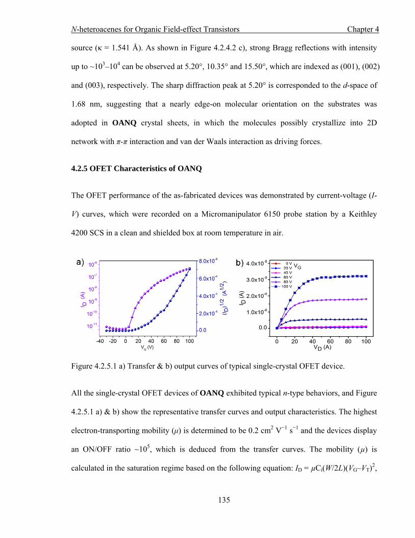
N-heteroacenes for Organic Field-effect Transistors Chapter 4
135
source (κ = 1.541 Å). As shown in Figure 4.2.4.2 c), strong Bragg reflections with intensity
up to ~103–104 can be observed at 5.20°, 10.35° and 15.50°, which are indexed as (001), (002)
and (003), respectively. The sharp diffraction peak at 5.20° is corresponded to the d-space of
1.68 nm, suggesting that a nearly edge-on molecular orientation on the substrates was
adopted in OANQ crystal sheets, in which the molecules possibly crystallize into 2D
network with π-π interaction and van der Waals interaction as driving forces.
4.2.5 OFET Characteristics of OANQ
The OFET performance of the as-fabricated devices was demonstrated by current-voltage (I-
V) curves, which were recorded on a Micromanipulator 6150 probe station by a Keithley
4200 SCS in a clean and shielded box at room temperature in air.
Figure 4.2.5.1 a) Transfer & b) output curves of typical single-crystal OFET device.
All the single-crystal OFET devices of OANQ exhibited typical n-type behaviors, and Figure
4.2.5.1 a) & b) show the representative transfer curves and output characteristics. The highest
electron-transporting mobility (μ) is determined to be 0.2 cm2 V−1 s−1 and the devices display
an ON/OFF ratio ~105, which is deduced from the transfer curves. The mobility (µ) is
calculated in the saturation regime based on the following equation: ID = µCi(W/2L)(VG–VT)2,

N-heteroacenes for Organic Field-effect Transistors Chapter 4
136
where ID is the drain-source current, µ is the field-effect mobility, Ci is the gate dielectric
capacitance, VG is the gate voltage, VT is the threshold voltage, W and L are the channel width
and length, respectively. It was noteworthy that the devices exhibited excellent air-stability
and there was no obvious mobility degradation observed even after one month storage in
ambient conditions.
4.2.6 Results Discussion
Figure 4.2.6.1 Electron density distribution of HOMO and LUMO levels of THNQ &
OANQ.
Molecular calculation was conducted to investigate the electron density distributions of
THNQ and OANQ with the same method illustrated in 2.2.6 Mechanism Discussion. As
shown in Figure 4.2.6.1, the HOMO coefficient of THNQ is distributed on the whole
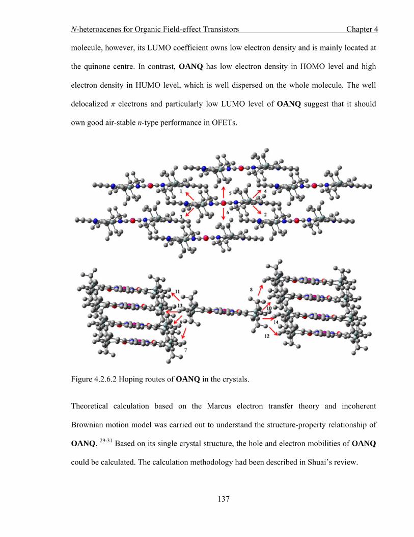
N-heteroacenes for Organic Field-effect Transistors Chapter 4
137
molecule, however, its LUMO coefficient owns low electron density and is mainly located at
the quinone centre. In contrast, OANQ has low electron density in HOMO level and high
electron density in HUMO level, which is well dispersed on the whole molecule. The well
delocalized π electrons and particularly low LUMO level of OANQ suggest that it should
own good air-stable n-type performance in OFETs.
Figure 4.2.6.2 Hoping routes of OANQ in the crystals.
Theoretical calculation based on the Marcus electron transfer theory and incoherent
Brownian motion model was carried out to understand the structure-property relationship of
OANQ. 29-31 Based on its single crystal structure, the hole and electron mobilities of OANQ
could be calculated. The calculation methodology had been described in Shuai’s review.
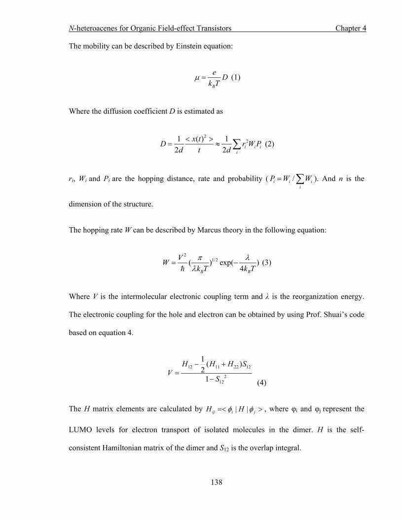
N-heteroacenes for Organic Field-effect Transistors Chapter 4
138
The mobility can be described by Einstein equation:
(1)
Where the diffusion coefficient D is estimated as
(2)
ri, Wi and Pi are the hopping distance, rate and probability ( ). And n is the
dimension of the structure.
The hopping rate W can be described by Marcus theory in the following equation:
(3)
Where V is the intermolecular electronic coupling term and λ is the reorganization energy.
The electronic coupling for the hole and electron can be obtained by using Prof. Shuai’s code
based on equation 4.
12 11 22 12
212
1( )
21
H H H SV
S
(4)
The H matrix elements are calculated by | |ij i jH H , where φi and φj represent the
LUMO levels for electron transport of isolated molecules in the dimer. H is the self-
consistent Hamiltonian matrix of the dimer and S12 is the overlap integral.
B
eD
k T
221 ( ) 1
2 2 i i ii
x tD r W P
d t d
/i i ii
P W W
21/2( ) exp( )
4B B
VW
k T k T
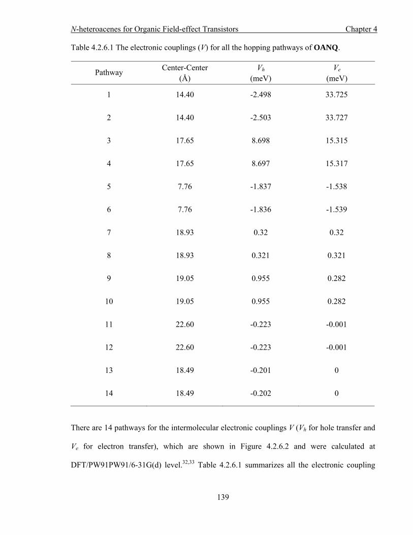
N-heteroacenes for Organic Field-effect Transistors Chapter 4
139
Table 4.2.6.1 The electronic couplings (V) for all the hopping pathways of OANQ.
Pathway Center-Center
(Å) Vh
(meV) Ve
(meV)
1 14.40 -2.498 33.725
2 14.40 -2.503 33.727
3 17.65 8.698 15.315
4 17.65 8.697 15.317
5 7.76 -1.837 -1.538
6 7.76 -1.836 -1.539
7 18.93 0.32 0.32
8 18.93 0.321 0.321
9 19.05 0.955 0.282
10 19.05 0.955 0.282
11 22.60 -0.223 -0.001
12 22.60 -0.223 -0.001
13 18.49 -0.201 0
14 18.49 -0.202 0
There are 14 pathways for the intermolecular electronic couplings V (Vh for hole transfer and
Ve for electron transfer), which are shown in Figure 4.2.6.2 and were calculated at
DFT/PW91PW91/6-31G(d) level.32,33 Table 4.2.6.1 summarizes all the electronic coupling

N-heteroacenes for Organic Field-effect Transistors Chapter 4
140
values. The hole and electron reorganization energies of OANQ were calculated at the
DFT/B3LYP/6-31G(d) level to be 0.1253 eV and 0.1102 eV.34 The largest electron transfer
integrals of OANQ were aligned in 1, 2 and 3, 4 directions (Figure 4.2.6.2), which achieved
comparable results of 33.725 and 15.315 meV to the famous PDIs derivatives with calculated
transfer integral of 50 meV.35 The calculated hole and electron mobilities in room
temperature were determined to be 0.19 cm2 V-1 s-1 and 2.50 cm2 V-1 s-1, respectively, which
was well consistent with the experimental results.
4.2.7 Summary
In summary, a large π-conjugated N-heteroquinone OANQ containing 8 N atoms has been
designed and synthesized. The moderate conjugation and the slight twisted conformation on
the backbone of OANQ make it own good environmental stability. Combined with the
particular low LUMO level and 2D π-π stacking, OANQ displays high and air-stable
electron-transporting mobility up to 0.2 cm2 V-1 s-1 in the single-crystal OFET devices.
Besides that, the as-prepared devices show good environmental stability in ambient
laboratory conditions.
4.3 References
1 Laquindanum, J. G. Katz, H. E. Dodabalapur, A. & Lovinger, A. J. Journal of the
American Chemical Society 118, 11331-11332, (1996).
2 Shukla, D. Nelson, S. F. Freeman, D. C. Rajeswaran, M. Ahearn, W. G. Meyer, D. M.
& Carey, J. T. Chemistry of Materials 20, 7486-7491, (2008).

N-heteroacenes for Organic Field-effect Transistors Chapter 4
141
3 Stolte, M. Gsaenger, M. Hofmockel, R. Suraru, S.-L. & Wuerthner, F. Physical
Chemistry Chemical Physics 14, 14181-14185, (2012).
4 Zhao, Y. Di, C.-A. Gao, X. Hu, Y. Guo, Y. Zhang, L. Liu, Y. Wang, J. Hu, W. & Zhu,
D. Advanced Materials 23, 2448-2453, (2011).
5 Zhang, F. Hu, Y. Schuettfort, T. Di, C.-A.Gao, Y. McNeill, C. R. Thomsen, L.
Mannsfeld, S. C. B. Yuan, W. Sirringhaus, H. & Zhu, D. Journal of the American
Chemical Society 135, 2338-2349, (2013).
6 Tiwari, S. P. Kim, J. Knauer, K. A. Hwang, D. K. Polander, L. E. Barlow, S. Marder,
S. R. & Kippelen, B. Organic Electronics 13, 1166-1170, (2012).
7 Horowitz, G. Kouki, F. Spearman, P. Fichou, D. Nogues, C. Pan, X. & Garnier, F.
Advanced Materials 8, 242-&, (1996).
8 Chesterfield, R. J. McKeen, J. C. Newman, C. R. Ewbank, P. C. da Silva Filho, D. A.
S. Brédas, J.-L. Miller, L. L. Mann, K. R. & Frisbie, C. D. Journal of Physical
Chemistry B 108, 19281-19292, (2004).
9 Oh, J.-D. Seo, H.-S. Kim, D.-K. Shin, E.-S. & Choi, J.-H. Organic Electronics 13,
2192-2200, (2012).
10 Oh, J. H. Lee, H. W. Mannsfeld, S. Stoltenberg, R. M. Jung, E. & Jin, Y. W.
Proceedings of the National Academy of Sciences of the United States of America 106,
6065-6070, (2009).

N-heteroacenes for Organic Field-effect Transistors Chapter 4
142
11 Schmidt, R. Oh, J. K. Sun, Y.-S. Deppisch, M. Krause, A.-M. Radacki, K.
Braunschweig, H. Könemann, M. Erk, P. Bao, Z. & Würthner, F. Journal of the
American Chemical Society 131, 6215-6228, (2009).
12 Soeda, J. Uemura, T. Mizuno, Y. Nakao, A. Nakazawa, Y. Facchetti, A. & Takeya, J.
Advanced Materials 23, 3681-3685, (2011).
13 Molinari, A. S. Alves, H. Chen, Z. Facchetti, A. & Morpurgo, A. F. Journal of the
American Chemical Society 131, 2462-2463, (2009).
14 Minder, N. A. Ono, S. Chen, Z. Facchetti, A. & Morpurgo, A. F. Advanced Materials
24, 503-508, (2012).
15 Li, J. Chang, J.-J. Tan, H. S. Jiang, H. Chen, X. Chen, Z. Zhang, J. & Wu, J.
Chemical Science 3, 846-850, (2012).
16 Ando, S. Nishida J, Tada H, Inoue Y, Tokito S, & Yamashita Y. Journal of the
American Chemical Society 127, 5336-5337, (2005).
17 Ichikawa, M. Kato, T. Uchino, T. Tsuzuki, T. Inoue, M. Jeon, H.-G. Koyama, T. &
Taniguchi, Y. Organic Electronics 11, 1549-1554, (2010).
18 Yun, S. W. Kim, J. H. Shin, S. Yang, H. An, B.-K. Yang, L. & Park, S. Y. Advanced
Materials 24, 911-915, (2012).
19 Yoon, M.-H. Kim, C. Facchetti, A. & Marks, T. J. Journal of the American Chemical
Society 128, 12851-12869, (2006).

N-heteroacenes for Organic Field-effect Transistors Chapter 4
143
20 Fischer, O. & Hepp, E. Berichte der deutschen chemischen Gesellschaft 23, 2789-
2793, (1890).
21 Hinsberg, O. Justus Liebigs Annalen der Chemie 319, 257-286, (1901).
22 Miao, Q. Nguyen, T. Q. Someya, T. Blanchet, G. B. & Nuckolls, C. Journal of the
American Chemical Society 125, 10284-10287, (2003).
23 Ma, Y. Q. Sun, Y. M. Liu, Y. Q. Gao, J. H. Chen, S. Sun, X, B, Qiu, W. F. Yu, G.
Cui, G. L. Hu, W. P. & Zhu, D. B. Journal of Materials Chemistry 15, 4894-4898,
(2005).
24 Islam, M. M. Pola, S. & Tao, Y.-T. Chemical Communications 47, 6356-6358, (2011).
25 Liang, Z. Tang, Q. Xu, J. & Miao, Q. Advanced Materials 23, 1535-1539, (2011).
26 Dong, H. Fu, X. Liu, J. Wang, Z. & Hu, W. Advanced Materials 25, 6158-6183,
(2013).
27 Anthony, J. E. Brooks, J. S. Eaton, D. L. & Parkin, S. R. Journal of the American
Chemical Society 123, 9482-9483, (2001).
28 Lindner, B. D. Engelhart, J. U. Tverskoy, O. Appleton, A. L. Rominger, F. Peters, D.-
C. A. Himmel, H.-J. & Bunz. U. H. F. Angewandte Chemie-International Edition 50,
8588-8591, (2011).
29 Deng, W. Q. & Goddard, W. A. Journal of Physical Chemistry B 108, 8614-8621,
(2004).

N-heteroacenes for Organic Field-effect Transistors Chapter 4
144
30 Bredas, J. L. Beljonne, D. Coropceanu, V. & Cornil, J. Chemical Reviews 104, 4971-
5003, (2004).
31 Marcus, R. A. Reviews of Modern Physics 65, 599-610, (1993).
32 Valeev, E. F. Coropceanu, V. da Silva Filho, D. A. Salman, S. & Bredas, J.-L.
Journal of the American Chemical Society 128, 9882-9886, (2006).
33 Troisi, A. & Orlandi, G. Journal of Physical Chemistry B 106, 2093-2101, (2002).
34 Song, Y. Di, C. Yang, X. Li, S. Xu, W. Liu, Y. Yang, L. Zhuai, Z. Zhang, D. & Zhu,
D. Journal of the American Chemical Society 128, 15940-15941, (2006).
35 Geng, H. Peng Q, Wang L, Li H, Liao Y, Ma Z, Shuai Z. Advanced Materials 24,
3568-3572, (2012).
Conclusions & Future Work Chapter 5
145
Chapter 5
Conclusions & Future Work
5.1 Conclusions
A series of D-A molecules with novel N-heteroacenes as acceptors have been designed and
synthesized for ORMs application, based on two series of hypothesis: different N-
heteroacene units can induce multiple electron “traps” and strong electron-deficient N-
heteroacenes can be used as acceptors to induce multiple electrons intermolecular charge
transfer. When imidazole and pyrazine are combined together as a single acceptor moiety,
only two-state non-volatile memory behaviors can be observed. Probably the acceptor moiety
acts as a single electron “trap” or the memory behaviors are induced by intermolecular
charge transfer. Increasing the acceptor moieties shows no obvious influence on the
switching process of molecules, although the morphology of films does affect the ON/OFF
ratio. When strong electron-deficient N-heteroacene acceptor is combined with multiple
donors, the molecule show multilevel, rewritable, non-volatile memory behaviors, which
ware possibly induced by multiple electrons intermolecular charge transfer. The success
indicates an efficient molecule designing strategy to develop multilevel memory materials.
The novel D-π-A small molecule with a large N-heteroacene as acceptor moiety and widely
explored benzo[1,2-b:4,5-b’]dithiophene (BDT) as a donor has been synthesized and
characterised for OPVs. The molecule is expected to own high OPV performance resulting
from the increased conjugation. The as-fabricated OPV device through solution-processing
method shows a PCE of 1.97%. MoO3 has been proved to be a useful anode buffer layer for
Conclusions & Future Work Chapter 5
146
this type of materials and the enhanced performance probably comes from the more aligned
energy level between the working function of MoO3 and the HOMO level of molecule, and
the reduced chemical interactions between MoO3 and organic film. Although there is a gap
between our results of PCE at 1.97% and the highest record in literature, it is believed that
large N-heteroacenes have the potential to be applied as good acceptor moieties and after
structure modification, better performance can probably be achieved.
The large π-conjugated N-heteroquinone has been designed and synthesized through
convenient condensation reaction, which has 8 N atoms in its backbone with lineally fused
structure. The existence of quinone centre makes the as-prepared N-heteroquinone own
relatively moderate conjugation level, thus it has good stability. A particularly deep LUMO
level lower than -4.0 eV is obtained by introducing more N atoms, which makes it have the
potential to be applied as air-stable n-type materials. The single-crystal OFET devices based
on the as-prepared N-heteroquinone show charming electron-transporting mobility up to 0.2
cm2 V-1 s-1 when measured under ambient condition, and the devices can maintain the good
performance for long period. Based on the theoretical calculation, there is large space to be
filled for the OFET performance of this type of N-heteroquinone materials, although our
initial results are out of the highest records. It is noteworthy that the excellent operational
stability of our N-heteroquinone makes it shine among the other reported air-stable n-type
materials. It is believed that more inspiring results can be achieved after molecular
modification based on the as-designed N-heteroquinone, and the design of large π-conjugated
N-heteroquinones is a promising way to develop novel air-stable n-type materials.

Conclusions & Future Work Chapter 5
147
5.2 Future Work of N-heteroacenes for Organic Memories
Scheme 5.2.1 Synthetic route for the typical donor units.
Scheme 5.2.2 Synthetic route for target D-A molecules.

Conclusions & Future Work Chapter 5
148
We have found an efficient way to achieve rewritable, multilevel memory materials by
combining strong electron-deficient N-heteroacenes and multiple triphenylamine (TPA)
donor units. On the basis of these studies, we will further investigate the designing strategy
and expand it to be available for more types of donor units. Thus, various typical donor units
will be synthesized from BDT, thiophene or carbazole (shown in Scheme 5.2.1).
The typical donor units will be combined with the successful 5,12-
bis((triisopropylsilyl)ethynyl)-1,4,6,11-tetraazatetracene (BTTT) acceptor moiety in similar
procedure illustrated in 2.4.2 Synthesis of 2TPA-BTTT (shown in Scheme 5.2.2). It is
expected that the as-designed molecules will display similar rewritable and multilevel
switching behaviors with that of 2TPA-BDTT. Through comparing the memory properties
of these molecules, one type of ultimate material with good endurance and easy to control
will be potentially achieved.
5.3 Future Work of N-heteroacens for Organic Photovoltaics
The morphology and crystallinity of molecules in solid states have proved to greatly affect
the OPV performance. We have demonstrated that the D-π-A molecules with large N-
heteroacens as acceptors can be utilized as donor materials for OPV application, although
their initial performance is quite behind of the highest records. The molecular side chains
have been reported to play an important role for determining the morphology and
crystallinity of films, and the selection of suitable side chains is critical for developing high
performance OPV materials. Considering these factors, various side chains will be introduced
onto 4,11-bis((triisopropylsilyl)ethynyl)-1H-imidazo[4,5-b]phenazine (BIP) moiety, and
novel D-π-A small molecules 7a–c (shown in Scheme 5.3.1) are proposed. More inspiring

Conclusions & Future Work Chapter 5
149
Scheme 5.3.1 Synthetic route for 7a–c.
OPV performance based on these molecules is expected.
5.4 Future Work of N-heteoacenes for Organic Field-effect Transistors
Scheme 5.3.1 Synthetic route for 8.
Conclusions & Future Work Chapter 5
150
As the conjugation of OANQ is increased, a deeper LUMO level should be achieved, which
is expected to enhance the n-type performance of molecules in ambient conditions. Thus, the
possibility will be investigated by changing the carbonyl groups with alkyl chains, in which
situation a nonacene analogue 8 is designed (shown in Scheme 5.3.1). To date there is no
literature report about the semiconducting properties of large conjugated nonacenes because
of their tough synthesis and instability. Hence, the properties investigation of 8 is challenging
and significant for both fundamental study and practical application, and 8 is expected to own
charming n-type performance in OFETs.
Publications during Ph. D. Candidate Appendixes
151
Appendixes
Publications during Ph. D. Candidate
1. Wang, C.‡ Zhang, J.‡ Long, G. Aratani, N. Yamada, H. Zhao, Y. & Zhang, Q.
Synthesis, structure and air-stable n-type field-effect transistor behaviors of
functionalized octaazanonacene-8,19-dione. Angewandte Chemie-International
Edition 54, 6292-6296, (2015)
2. Wang, C. Hu, B. Wang, J. Gao, J. Li, G. Xiong, W. Zou, B. Suzuki, M. Aratani, N.
Yamada, H. Huo, F. Lee, P. S. & Zhang, Q. Rewritable multilevel memory
performance of a tetraazatetracene donor-acceptor derivative with good endurance.
Chemistry-An Asian Journal 10, 116-119, (2015)
3. Wang, C. Wang, J. Li, P. Gao, J. Tan, S. Y. Xiong, W. Hu, B. Lee, P. S. Zhao, Y.
& Zhang, Q. Synthesis, characterization, non-volatile memory device application of a
novel N-substituted heteroacene. Chemistry-An Asian Journal 9, 779-783, (2014)
4. Wang, C. Li, G. & Zhang, Q. A novel heteroacene 2-(2,3,4,5-tetrafluorophenyl)- 1H-
imidazo[4,5-b]phenazine as a multi-response sensor for F- detection. Tetrahedron
Letters 54, 2633-2636 (2013).
5. Wang, C.‡ Okabe,‡ T. Long, G. Kuzuhara, D. Zhao, Y. Aratani, N. Yamada, H.
& Zhang, Q. A novel D-π-A small molecule with N-heteroacene as acceptor moiety
for photovoltaic application. Dyes and Pigments 122, 231-237 (2015)
Publications during Ph. D. Candidate Appendixes
152
6. Wang, C. Yamashita, M. Hu, B. Zhou, Y. Wang, J. Wu, J. Huo, F. Lee, P. S.
Aratani, N. Yamada, H. & Zhang, Q. Synthesis, characterization and memory
performance of two organic small molecules through donor-acceptor design. Asian
Journal of Organic Chemistry 4, 646-651 (2015)
7. Hu, B. Wang, C. Wang, J. Gao, J. Wang, K. Wu, J. Zhang, G. Cheng, W.
Venkateswarlu, B. Wang, M. Lee, P. S. & Zhang, Q. Inorganic-organic hybrid
polymer with multiple redox for high-density data storage. Chemical Science 5, 3404-
3408, (2014)
8. Zhang, J. Wang, C. Chen, W. Wu, J. & Zhang, Q. Fabrication and physical properties
of self-assembled ultra-long polymer/small molecule hybrid microstructures. RSC
Advances 5, 25550-25554, (2015)
9. Hu, B. Wang, C. Zhang, J. Qian, K. Chen, W. Lee, P. S. & Zhang, Q. Water-soluble
conjugated polymers as active elements for organic nonvolatile memories. RSC
Advances 5, 30542-30548, (2015)
10. Li, G. Wu, Y. Gao, J. Wang, C. Li, J. Zhang, H. Zhao, Y. Zhao, Y. & Zhang, Q.
Synthesis and physical properties of four hexazapentacene derivatives. Journal of the
American Chemical Society 134, 20298-20301, (2012)
11. Gu, P. Zhou, F. Gao, J. Li, G. Wang, C. Xu, Q. Zhang,Q. & Lu, J. Synthesis,
characterization and nonvolatile ternary memory behavior of a
larger heteroacene with nine linearly-fused rings and two different
heteroatoms. Journal of the American Chemical Society 135, 14086-14089, (2013)
Publications during Ph. D. Candidate Appendixes
153
12. Wu, J. Rui, X. Wang, C. Pei, W. Lau, R. Yan, Q. & Zhang, Q. Nanostructured
conjugated ladder polymers for stable and fast lithium storage anodes with high-
capacity. Advanced Energy Materials 5, 1402189, (2015)
13. Li, G. Zheng, K. Wang, C. Leck, K. S. Hu, F. Sun, X. W. & Zhang, Q. Synthesis
and nonvolatile memory behaviors of dioxatetraazapentacene derivatives. ACS
Applied Materials Interfaces 5, 6458-6462, (2013)
14. Gu, P. Gao, J. Lu, C. Wang, C. Li, G. Zhou, F. Xu, Q. Lu, J. & Zhang, Q. Synthesis
of tetranitro-oxacalix[4]arene with oligoheteroacene groups and its nonvolatile
ternary memory performance. Materials Horizon 1, 446-451, (2014)
15. Zhou, Y. Pei, W. Wang, C. Zhu, J. Wu, J. Yan, Q. Huang, L. Huang, W. Yao, C. Loo,
J. & Zhang, Q. Rhodamine-modified upconversion nanophosphors for ratiometric
detection of hypochlorous acid in aqueous solution and living cells. Small 10, 3560-
3567, (2014)
16. Huang, X. Yu, H. Tan, H. Zhu, J. Zhang, W. Wang, C. Zhang, J. Wang, Y. Lv, Y.
Zeng, Z. Liu, D. Ding, J. Zhang, Q. Srinivasan, M. Ajayan, P. Hng, H. H. & Yan, Q.
Carbon nanotubes(CNTs)-encapsulated noble metal nanoparticles hybrid as cathode
materials for Li-oxygen batteries. Advanced Functional Materials 41, 6516-6523,
(2014)
17. Gu, P. Ma, Y. He, J. Long, G. Wang, C. Chen, W. Liu, Y. Xu, Q. Lu, J. & Zhang, Q.
Substituent groups effect on the morphology and memory performance of phenazine
derivatives. Journal of Materials Chemistry C DOI: 10.1039/C5TC00003C, (2015)

Publications during Ph. D. Candidate Appendixes
154
18. Zhao, J. Wong, J. Wang, C. Gao, J. Ng, V. Yang, H. Loo, J. & Zhang, Q. Synthesis,
physical properties and self-assembly of a novel asymmetric aroyleneimidazo-
phenazine. Chemistry-An Asian Journal 8, 665-669, (2013)
19. Zhou, Y. Chen, W. Zhu, J. Pei, W. Wang, C. Huang, L. Yao, C. Yan, Q. Huang, W.
Loo, J. & Zhang, Q. Inorganic-organic hybrid nanoprobe for NIR-excited imaging of
hydrogen sulfide in cell cultures and inflammation in a mouse model. Small 10, 4874-
4885, (2014)
20. Gu, P. Zhao, Y. He, J. Zhang, J. Wang, C. Xu, Q. Lu, J. Sun, X. & Zhang, Q.
Synthesis, physical properties, and light-emitting diode performance of phenazine-
based derivatives with three, five and nine fused six-member rings. Journal of
Organic Chemistry DOI: 10.1021/jo5027707, (2015)
21. Zhao, J. Li, G. Wang, C. Chen, W. Loo, J. & Zhang, Q. A new N-
substituted heteroacene can detect CN- and F- anions via anion-π interaction. RSC
Advances 3, 9653-9657, (2013)


![A Cationic Water-Soluble Pillar[6]arene: Synthesis, Host ... · A Cationic Water-Soluble Pillar[6]arene: Synthesis, Host–Guest Properties, and Self-Assembly with Amphiphilic Guests](https://static.fdocuments.in/doc/165x107/60616c387c76dc33b6079e27/a-cationic-water-soluble-pillar6arene-synthesis-host-a-cationic-water-soluble.jpg)


![A cationic water-soluble pillar[5]arene: synthesis and ... · S1 A cationic water-soluble pillar[5]arene: synthesis and host − guest complexation with sodium 1-octanesulfonate Yingjie](https://static.fdocuments.in/doc/165x107/60616c387c76dc33b6079e25/a-cationic-water-soluble-pillar5arene-synthesis-and-s1-a-cationic-water-soluble.jpg)