Design of ULP circuits for Harvesting applications
145
HAL Id: tel-02408334 https://tel.archives-ouvertes.fr/tel-02408334 Submitted on 13 Dec 2019 HAL is a multi-disciplinary open access archive for the deposit and dissemination of sci- entific research documents, whether they are pub- lished or not. The documents may come from teaching and research institutions in France or abroad, or from public or private research centers. L’archive ouverte pluridisciplinaire HAL, est destinée au dépôt et à la diffusion de documents scientifiques de niveau recherche, publiés ou non, émanant des établissements d’enseignement et de recherche français ou étrangers, des laboratoires publics ou privés. Design of ULP circuits for Harvesting applications Nicola Verrascina To cite this version: Nicola Verrascina. Design of ULP circuits for Harvesting applications. Electronics. Université de Bordeaux, 2019. English. NNT : 2019BORD0115. tel-02408334
Transcript of Design of ULP circuits for Harvesting applications

HAL Id: tel-02408334https://tel.archives-ouvertes.fr/tel-02408334
Submitted on 13 Dec 2019
HAL is a multi-disciplinary open accessarchive for the deposit and dissemination of sci-entific research documents, whether they are pub-lished or not. The documents may come fromteaching and research institutions in France orabroad, or from public or private research centers.
L’archive ouverte pluridisciplinaire HAL, estdestinée au dépôt et à la diffusion de documentsscientifiques de niveau recherche, publiés ou non,émanant des établissements d’enseignement et derecherche français ou étrangers, des laboratoirespublics ou privés.
Design of ULP circuits for Harvesting applicationsNicola Verrascina
To cite this version:Nicola Verrascina. Design of ULP circuits for Harvesting applications. Electronics. Université deBordeaux, 2019. English. NNT : 2019BORD0115. tel-02408334

THÈSE PRÉSENTÉE
POUR OBTENIR LE GRADE DE
DOCTEUR DE
L’UNIVERSITÉ DE BORDEAUX
SPI
Electronique
Par Verrascina Nicola
Design of ULP circuits for harvesting applications
Sous la direction de : Jean-Baptiste Begueret
(co-directeur : Mattia Borgarino) Soutenue le 05/07/2019 Membres du jury : M. Thierry Tarris PB Président M. Hervé Barthelémy Université Toulon-Var Rapporteur M. Patrice Gamand XLIM Examinateur M. Nicola Regimbal Invyssis Examinateur

Titre : Conception des circuits à très faible consommation pour des applications Harvesting
Résumé : La très faible consommation dans les appareilles modernes
est le facteur-clé pour les capteurs alimentée par une source d’énergie récupérée. La réduction du budget de puissance peut être atteinte grâce à différents techniques lié à trois niveaux d’abstraction : transistor, circuit et système. L’objet de cette thèse est l’analyse et la conception des circuits à très faible consommation pour des réseaux des capteurs sans fils. A’ régulateur de tension et an émetteur RF ont été examiné. Le premier est le circuit principal pour la gestion de puissance ; il agit comme interface entre le transducteur et les autres circuits du capteur. L’metteur est le circuit que exiges le plus de puissance pour fonctionner, donc une réduction de sa puissance il permet une augmentation de la vie opérationnelle du capteur.
Mots clés : WSN, régulateur de tension, émetteur courte portée
Title: Design of Ultra Low-Power Circuits for Harvesting Applications
Abstract: In the modern devices Ultra-low power consumption is the
survival key for the energy-harvested sensor node. The reduction of the power budget can be achieved by mixing different low–power techniques at three levels of abstraction: transistor level, circuit level and system level. This thesis deals with the analysis and the design of Ultra-Low Power (ULP) circuits suitable for Energy-Harvesting Wireless Sensor Networks (EHWSN). In particular, voltage regulator and RF transmission circuits are examined. The former is the main block in power management unit; it interfaces the transducer circuit with the rest of the sensor node. The latter is the most energy hungry block and thus decreasing its power consumption can drastically increases the sensor on-time.
Keywords: WSN, LDO, Short-range transmitter, Data-rate
L a b o r a t o i r e d e l ' I n t é g r a t i o n d u M a t é r i a u a u S y s t è m e
351 Cours de la libération, 33405 Talence cedex, France

"To those who ght for the freedom"

Abstract
The increasing diusion of Wireless Sensor Node (WSNs) and Body-Area sensor Network(BAN) is mainly due to the demand of smart environment in order to increase the qualityof life. Several are the application domains:from domotic to industry, from medicine torural applications. Normally a sensor network counts huge number of sensors that maybe placed in hostile environment. Many time the batteries replacement is hard and ex-pensive.Therefore the need to nd another type of energy source, replacing the batteries,has created an increasing interest in the scientic academy.The development of new material and the technological progress have supported the pos-sibility to extract the energy from non-conventional sources for small scale applications.However the amount of energy density is not high as it spans from the highest value of500 µW/cm2 for solar source to the lowest one of 1 µ W/ cm2 for radio-frequency source.The energy constraint poses a several challenge for the designers to extend the lifetimedevices. Ultra-low power consumption is the survival key for the energy-harvested sensornode. The reduction of the power budget can be achieved by mixing dierent low -powertechniques at three levels of abstraction: transistor level, circuit level and system level.This thesis deals with the analysis and the design of Ultra-Low Power (ULP) circuits suit-able for Energy-Harvesting Wireless Sensor Networks (EHWSN). In particular, voltageregulator and RF transmission circuits are examined. The former is the main block inpower management unit; it interfaces the transducer circuit with the rest of the sensornode. The latter is the most energy hungry block and thus decreasing its power consump-tion can drastically increases the sensor on-time.The thesis is structured as follows:Chapter 1 describes the harvesting sources available in the environment, highlighting foreach of them the main advantages and drawbacks when they are applied in small scaledevices. The second part of this chapter is dedicated to the low-power techniques. Threelevels of abstraction are introduced (CMOS technology, Circuit and System) with theiradvantages and drawbacks.Chapter 2 is dedicated to the study of wireless sensor networks. A general framework isgiven on the sensor architecture with highlights on the fundamental blocks. The expres-sion for the required radiated power is obtained for a given distance. The duty-cycledequation is also obtained to get the best trade-o in terms of required energy, communi-cation channel quality and amount of data transfer.Chapter 3 focuses on the design of very ecient Low-DropOut voltage (LDO) regulator.Many are the eorts to achieve a good regulation accuracy by addressing ultra low powerconsumption. Especially for transient response the closed loop frequency response andthe slew-rate of the error amplier requires high quiescent current to achieve good per-formances. In this work an adaptively bias current and a class-AB error amplier areimplemented in such way the increase in quiescent current is proportional to the verylarge load current. With these techniques the impact on the global power consumption ofLDO is reduced. Moreover high current eciency for all load conditions is also achieved.The stability of closed loop is ensured by a current buer and a Miller's capacitor forthe whole range of operational load current. The stability is guaranteed also for very lowstand-by current.
In chapter 4 the design ow of OOK modulation transmitter is addressed. The low tar-geted radiated power of -15 dBm poses a severe limitation for the global transmittereciency. The rst part of the chapter is dedicated to the study of classical cascadedarchitectures where the oscillator (VCO) is directly connected to the input of the powerdriver. The trade-o between the supply voltage and the matching network is describedhighlighting the diculty to integrate the passive elements of matching network when thesupply voltage for the power amplier is about 1 V and the peak to peak output voltagerequired over a 50 Ω is in the order of tens millivolts. To circumnavigate this problem acurrent reuse transmitter is proposed where the power driver and the VCO are stackedand the same bias current is used. With this architecture the supply voltage can be tunedbetween the two circuits to achieve the best trade-o between the power consumption andthe performances of each circuit.

Résumé
La demande toujours croissante d'amélioration de la qualité de vie avec la création desenvironnements intelligents, a permis la diusion des reseaux des capteurs sans l. Lesapplications envisagées peuvent aller de la domotique à l'industrie, de la medicine à l'agri-culture. Le probléme principal pour ces types des capteurs est le remplacement des bat-teries, étant donné que l'installation pourrait avoir lieu dans des environnement hostiles.Donc la recherche d' autres types des sources d'énergie qui peuvent remplacer les batteriesa attiré l'attention de la Communauté scientique internationale.Nombreux sont les sources à partir des quelles il est possible obtenir de l'énergie électriquepour des systèmes miniaturisés. Néanmoins la faible énergie mise à disposition par dessources non-conventionnelles, pose un vrai dé pour les concepteurs s'ils veulent augmen-ter la durée de vie des systèmes. C'est seulement par l'utilisation des circuits à trés faibleconsommation que les capteures autonomes peuvent représenter un choix valable pourle marché. La réduction du besoin d'énergie peut être atteinte en mélegeant diérentestecniques à trois diérent niveaux d'abstraction : transistor, circuit et système.L'objectif de la thése est la conception et l'analyse des circuits à trés faible consom-mation appropriés pour des applications d' Energy-Harvesting Wireless Sensor Networks(EHWSN). La première partie détaille le régulateur de tension, qui est le circuit fon-damental du bloc dédiée à la gestion de la puissance. La deuxième partie est dédié àl'analyse et à la conception d'un emetteur RF, qui représente le circuit avec la consom-mation de puissance la plus haute présent dans le capteur. Par conséquent une reductionde la consommation de ce dernier circuit, baisse considérablement la démande d'énergiedu systeme dans sa totalité.La thése est ainsi organisée : Le chapitre 1 décrit les sources de récupération d'énergiedisponibles dans l'environnement, soulignant les avantages et les inconvénients quand ellesont appliquées à des circuits miniaturisés. La deuxième partie est dédiée à l'étude destechniques permettant la réduction de la consommation de puissance.Le chapitre 2 est dédié à l'étude des réseaux de capteurs sans l. Un cadre genéral deleur architecure est donné. L'équation pour calculer la puissance radiative nécessaire pourcouvrir une certaine distance est donnée. En dernier lieu le rapport cyclic optimale estderivée à partir de l'énergie nécessaire, de la qualité du canal de communication et de laquantité des données à transmettre.Le chapitre 3 décrit la conception d'un régulateur Low-DropOut (LDO) à haute eca-cité. L'attention est centrée pour obtenir une trés faible consommation de puissance sanssous-estimer la précision du réglage de tension. Pour obtenir un bonne réglage de tension,l'amplicateur d'erreurs doit avoir un slew-rate élevé, et la réponse en fréquence de laboucle, donc la vitesse de réglage du circuit, doit etre rapide. Les solutions adoptées poursurmonter le probléme sont un amplicateur d'erreur de classe-AB, avec un courant depolarisation qui s'adapte au courant de sortie du régulateur. L'ecacité est élevée pourtoutes les conditions du courant de sortie avec moins d'impact sur la consommation depuissance globale du circuit. La stabilité de la boucle est assurée dans toutes les condi-tions par un buer de courant et une capacité Miller, meme pour un courant trés faiblede stand-by en sortie. Le chapitre 4 décrit la conception d'un émetteur avec une modu-lation OOK. La faible puissance émise de -15 dBm limite l'ecacité globale du systém.

La premiére partie du chapitre est dédiée à l'étude d une structure classique en cascade,où la sortie du synthétiseur de fréquence (VCO) est directement connectée à l'entrée del'amplicateur de puissance. Le chapitre continue présentant les compromis de conceptionpour le réseau d'adaptation quand la tension d'alimentation est élevée alors que la tensionaux bor de la charge de 50 Ω est de quelques mV. Une architecture empilée est nalementproposée, où le VCO et le driver de puissance partagent le meme courant de polarisation,an de répartir la tension d'alimentation entre les deux circuits.

Contents
1 Low Power techniques for energy harvesting system 1
1.1 Energy Harvesting . . . . . . . . . . . . . . . . . . . . . . . . . . . . . . . 11.1.1 Solar Energy . . . . . . . . . . . . . . . . . . . . . . . . . . . . . . 11.1.2 Thermal Energy . . . . . . . . . . . . . . . . . . . . . . . . . . . . . 31.1.3 Kinetic Energy . . . . . . . . . . . . . . . . . . . . . . . . . . . . . 41.1.4 Radio-Frequency Energy . . . . . . . . . . . . . . . . . . . . . . . . 4
1.2 Design techniques for ULP circuits . . . . . . . . . . . . . . . . . . . . . . 51.2.1 CMOS level . . . . . . . . . . . . . . . . . . . . . . . . . . . . . . . 51.2.2 Circuit Level . . . . . . . . . . . . . . . . . . . . . . . . . . . . . . 71.2.3 System level . . . . . . . . . . . . . . . . . . . . . . . . . . . . . . . 111.2.4 Conclusion . . . . . . . . . . . . . . . . . . . . . . . . . . . . . . . . 13
2 System Approach 14
2.1 Energy Management . . . . . . . . . . . . . . . . . . . . . . . . . . . . . . 192.2 Link budget, data rate and duty cycle. . . . . . . . . . . . . . . . . . . . . 22
2.2.1 Required link Budget . . . . . . . . . . . . . . . . . . . . . . . . . . 222.2.2 Data Rate and Duty Cycle Trade-o. . . . . . . . . . . . . . . . . . 262.2.3 Conclusions . . . . . . . . . . . . . . . . . . . . . . . . . . . . . . . 28
3 Voltage Regulator 29
3.1 Background . . . . . . . . . . . . . . . . . . . . . . . . . . . . . . . . . . . 293.2 Voltage Regulator . . . . . . . . . . . . . . . . . . . . . . . . . . . . . . . . 30
3.2.1 Static Characteristics . . . . . . . . . . . . . . . . . . . . . . . . . . 313.2.2 Dynamic Characteristics . . . . . . . . . . . . . . . . . . . . . . . . 32
3.3 Switching versus Linear . . . . . . . . . . . . . . . . . . . . . . . . . . . . . 333.4 Low Drop-Out Regulator . . . . . . . . . . . . . . . . . . . . . . . . . . . . 373.5 Design Implementation . . . . . . . . . . . . . . . . . . . . . . . . . . . . . 45
3.5.1 Output Target . . . . . . . . . . . . . . . . . . . . . . . . . . . . . 453.5.2 Overcome current eciency-transient response trade-o . . . . . . . 473.5.3 Slew-rate enhancement . . . . . . . . . . . . . . . . . . . . . . . . . 493.5.4 Extended closed loop Bandwidth . . . . . . . . . . . . . . . . . . . 543.5.5 Compensation Strategy . . . . . . . . . . . . . . . . . . . . . . . . . 553.5.6 Transistor Level Design . . . . . . . . . . . . . . . . . . . . . . . . . 61
3.6 Voltage Reference . . . . . . . . . . . . . . . . . . . . . . . . . . . . . . . . 673.7 Circuit Design . . . . . . . . . . . . . . . . . . . . . . . . . . . . . . . . . . 713.8 Voltage Regulator Simulation Results . . . . . . . . . . . . . . . . . . . . . 743.9 Conclusion . . . . . . . . . . . . . . . . . . . . . . . . . . . . . . . . . . . . 82
i

CONTENTS
4 Ultra-Low power transmitter 83
4.1 Transmitter architecture . . . . . . . . . . . . . . . . . . . . . . . . . . . . 844.2 ULP Direct Modulation Transmitters. . . . . . . . . . . . . . . . . . . . . . 88
4.2.1 Local Oscillator . . . . . . . . . . . . . . . . . . . . . . . . . . . . . 884.2.2 Ring versus LC Oscillator . . . . . . . . . . . . . . . . . . . . . . . 904.2.3 Designing Low Power LC Oscillator . . . . . . . . . . . . . . . . . . 914.2.4 Power Amplier . . . . . . . . . . . . . . . . . . . . . . . . . . . . . 934.2.5 Comparison of dierent low power direct modulation transmitters . 964.2.6 Transmitter Design Steps . . . . . . . . . . . . . . . . . . . . . . . 964.2.7 Transmitter Simulation Results . . . . . . . . . . . . . . . . . . . . 106
4.3 Current Reuse Transmitter . . . . . . . . . . . . . . . . . . . . . . . . . . . 1094.3.1 Current Reuse VCO . . . . . . . . . . . . . . . . . . . . . . . . . . 1104.3.2 Designed current Reuse transmitter . . . . . . . . . . . . . . . . . . 114
4.4 Conclusion . . . . . . . . . . . . . . . . . . . . . . . . . . . . . . . . . . . . 119
5 Conclusions 120
A Drain current calculation in class AB Error Amplier 122
ii

List of Figures
1.1 Section of Photovoltaic Cell . . . . . . . . . . . . . . . . . . . . . . . . . . 21.2 Typical implementation of PV harvesting maximum power point tracking. 21.3 (a) Seedback eect, the generated voltage is proportional to the tempera-
ture gradient between the hot point TH and the cold point TC (b) Peltiereect the current generated by the applied voltage causes a thermal diu-sion from the heat dissipation to the heat absorption. . . . . . . . . . . . . 3
1.4 Cut-o Frequency trend in function of current density for dierent nodetechnology [WKvL+01] . . . . . . . . . . . . . . . . . . . . . . . . . . . . . 6
1.5 Combinations to achieve 8 nH inductance [Van15] where W is the metalwidth and N is the numbers of turns. . . . . . . . . . . . . . . . . . . . . . 7
1.6 Inversion coecient line number with voltage and shape factor MOSFETproperties [Bin07]. . . . . . . . . . . . . . . . . . . . . . . . . . . . . . . . 9
1.7 Minimum supply voltage required in classical cascode OTA when the tran-sistors are biased in strong and in moderate inversion. . . . . . . . . . . . . 10
1.8 Cascaded circuit block with two separate supply voltage and independentbias currents. . . . . . . . . . . . . . . . . . . . . . . . . . . . . . . . . . . 11
1.9 Multi-threshold application in logic circuit. . . . . . . . . . . . . . . . . . 111.10 Wake-up scheme timeline. . . . . . . . . . . . . . . . . . . . . . . . . . . . 12
2.1 Plot obtained from the measurement results for I = 2.3 mA and k = 1.25. 152.2 Market forecast for EH devices used in WSN applications. . . . . . . . . . 162.3 Energy Harvesting WSN market in 2012 (a) and prevision of market in
2017 (b) . . . . . . . . . . . . . . . . . . . . . . . . . . . . . . . . . . . . . 172.4 Power comparison between WSN and Energy Harvested circuit. . . . . . . 182.5 Architecure of energy harvesting sensor node. . . . . . . . . . . . . . . . . 192.6 Power management transistor level schematic implemented in [PCFP14] . 202.7 The top graph depicts an example of energy prole in harvesting system.
In the bottom graph the trend of voltage stored into the capacitor (redline) and the regulated voltage at the output of the PMU. . . . . . . . . . 21
2.8 Wireless sensor network mesh architecture . . . . . . . . . . . . . . . . . . 242.9 Wireless sensor network star architecture. . . . . . . . . . . . . . . . . . . . 252.10 RICER. . . . . . . . . . . . . . . . . . . . . . . . . . . . . . . . . . . . . . 25
3.1 Power Management Unit . . . . . . . . . . . . . . . . . . . . . . . . . . . . 293.2 General block diagram of voltage regulator . . . . . . . . . . . . . . . . . . 303.3 Load Regulation . . . . . . . . . . . . . . . . . . . . . . . . . . . . . . . . 313.4 Line Regulation . . . . . . . . . . . . . . . . . . . . . . . . . . . . . . . . . 32
iii

LIST OF FIGURES
3.5 Linear Regulator . . . . . . . . . . . . . . . . . . . . . . . . . . . . . . . . 343.6 Switching Regulator . . . . . . . . . . . . . . . . . . . . . . . . . . . . . . 353.7 Block Diagram of Buck Converter [WTM10] . . . . . . . . . . . . . . . . . 363.8 Regulated output voltage versus input voltage. . . . . . . . . . . . . . . . . 383.9 N-type and P-type pass element . . . . . . . . . . . . . . . . . . . . . . . . 383.10 Basic LDO Architecture . . . . . . . . . . . . . . . . . . . . . . . . . . . . 393.11 Typical transient Response of LDO regulator . . . . . . . . . . . . . . . . . 403.12 Energy balancing from light to heavy step . . . . . . . . . . . . . . . . . . 413.13 Energy balancing from heavy to light step . . . . . . . . . . . . . . . . . . 413.14 LDO negative feedback diagram . . . . . . . . . . . . . . . . . . . . . . . . 423.15 Poles movement with load current . . . . . . . . . . . . . . . . . . . . . . . 433.16 Parasitic gate capacitance Cg (a) and saturation drain-source volatage
Vsd−sat (b) of the pass transistor for dierent width W . . . . . . . . . . . 473.17 Class-A bias topology . . . . . . . . . . . . . . . . . . . . . . . . . . . . . . 493.18 Class-AB bias topology . . . . . . . . . . . . . . . . . . . . . . . . . . . . . 503.19 Class AB error amplier . . . . . . . . . . . . . . . . . . . . . . . . . . . . 513.20 FVF cell with cascode Pmos transistor . . . . . . . . . . . . . . . . . . . . 523.21 Gain Voltage (a) and SR (b) simulation for Ib= 60 nA for Class-AB error
amplier in solid line and class-A dot line. The simulations are performedwith CL=350 fF. . . . . . . . . . . . . . . . . . . . . . . . . . . . . . . . . 53
3.22 Adaptive biasing system. The rest of the circuit is omitted for simplicationpurposes . . . . . . . . . . . . . . . . . . . . . . . . . . . . . . . . . . . . . 54
3.23 Block Diagram of two stages amplier with current buer compensationtechnique . . . . . . . . . . . . . . . . . . . . . . . . . . . . . . . . . . . . 55
3.24 Transistor level design of the LDO voltage regulator proposed in this work 563.25 AB loop gain for dierent load current . . . . . . . . . . . . . . . . . . . . 573.26 LDO small-signal feedback representation . . . . . . . . . . . . . . . . . . . 583.27 KEX for dierent values of Ro−EA and gmp. The minimum value of separa-
tion factor is for light load condition. Ro−EA has negligible impact. . . . . . 603.28 KIN for dierent values of Ro−EA and gmp. The minimum value of separa-
tion factor is for light load condition.Also in this case Ro−EA has negligibleimpact. . . . . . . . . . . . . . . . . . . . . . . . . . . . . . . . . . . . . . . 61
3.29 The trend of the bias current adaptability versus the load current. . . . . . 623.30 LDO quiescent current and current eciency versus load current. In this
case the trend is shown only for operation mode (ILoad= 1 µA-1 mA).For stand-by mode the current eciency is worsen by the minimum draincurrent needed to keep ON the pass transistor. . . . . . . . . . . . . . . . . 62
3.31 (a) Open loop gain for ILoad = 1 µA (black line) and for ILoad = 1 mA (blueline). It is evident the GBW product is increased at heavy load conditiondue to higher GmEA. GBW extends from 40 kHz to 360 kHz (b) Phase forthe two load conditions. . . . . . . . . . . . . . . . . . . . . . . . . . . . . 63
3.32 Phase margin versus output capacitor value, for dierent stand-by outputcurrent values. From Istand−byL = 205 nA (dash line) to Ioperation−modeL = 1µA (solid line). . . . . . . . . . . . . . . . . . . . . . . . . . . . . . . . . . 64
3.33 Phase margin versus output capacitor value at heavy load condition . . . . 643.34 Phase margin versus output current for all operating regions. . . . . . . . . 653.35 Ueno voltage reference . . . . . . . . . . . . . . . . . . . . . . . . . . . . . 68
iv
LIST OF FIGURES
3.36 De Vita voltage reference . . . . . . . . . . . . . . . . . . . . . . . . . . . . 693.37 Bandgap Voltage reference proposed in [HUKN10] . . . . . . . . . . . . . 693.38 Sub-bandgap voltage reference used in this work . . . . . . . . . . . . . . . 713.39 Output voltage reference versus the temperature . . . . . . . . . . . . . . . 733.40 The quiescent current (a) and the voltage reference (b) versus supply voltage 733.41 Monte Carlo simulations on the output voltage reference with 100 runs. . 743.42 Line regulation (orange line) of LDO when VIN moves from 0 V to 1.6 V.
The simulation is performed at heavy load condition. . . . . . . . . . . . . 743.43 Output Voltage versus output current . . . . . . . . . . . . . . . . . . . . 753.44 Transient response for a load current step in operation mode. From 1 µA
to 1 mA. . . . . . . . . . . . . . . . . . . . . . . . . . . . . . . . . . . . . . 763.45 Transient response for a full load current step. From 300 nA to 1 mA. . . 773.46 Transient response for a load current step in moderate condition. From 300
µA to 1 mA. . . . . . . . . . . . . . . . . . . . . . . . . . . . . . . . . . . . 783.47 Line transient at heavy load condition . . . . . . . . . . . . . . . . . . . . 793.48 PSR at heavy load condition . . . . . . . . . . . . . . . . . . . . . . . . . . 793.49 Monte Carlo simulations on the phase margin with 100 runs.a) for stand-by
condition b) for minimum operating load condition . . . . . . . . . . . . . 803.50 Monte Carlo simulations on the regulator output voltage with 100 runs.
a) for minimum operating load condition b) for maximum operating loadcondition . . . . . . . . . . . . . . . . . . . . . . . . . . . . . . . . . . . . . 81
4.1 Block diagram of two-step conversion transmitter . . . . . . . . . . . . . . 844.2 Block diagram of direct modulation transmitter. . . . . . . . . . . . . . . . 844.3 FOM versus data-rate for recent ULP transmitter. [KPL17] . . . . . . . . . 864.4 Block diagram of sub-harmonic injection locking transmitter [PO11]. . . . 864.5 Power VCO transmitter presented in [MBL+13]. . . . . . . . . . . . . . . . 874.6 Current starved VCO . . . . . . . . . . . . . . . . . . . . . . . . . . . . . . 884.7 LC resonator with negative resistor to compensate the losses due to para-
sitic resistor RP . . . . . . . . . . . . . . . . . . . . . . . . . . . . . . . . . 894.8 Output voltage variation in presence of noisy source. At the left side the
noise is injected at the peak voltage, at the right side the noise is injectedat zero transition. . . . . . . . . . . . . . . . . . . . . . . . . . . . . . . . . 90
4.9 Transformation of series LC tank to parallel one. . . . . . . . . . . . . . . . 914.10 NMOS cross coupled LC oscillator. . . . . . . . . . . . . . . . . . . . . . . 924.11 CMOS LC oscillator . . . . . . . . . . . . . . . . . . . . . . . . . . . . . . 934.12 General representation of power amplier. . . . . . . . . . . . . . . . . . . 944.13 Transistor level schematic of direct modulation transmitters. Single voltage
supply for both VCO and PA (a), double voltage supply to optimize thePA eciency (b). . . . . . . . . . . . . . . . . . . . . . . . . . . . . . . . . 97
4.14 Bias point to perform class-C operation mode(a) typical voltage and cur-rent waveforms at the transistor drain(b) Biasing the transistor at voltagelower than the threshold voltage permits to reduce the voltage and currentoverlapping period. . . . . . . . . . . . . . . . . . . . . . . . . . . . . . . . 98
4.15 Implementation of L-matching network to transform 50 Ω to the optimumload resistance of 2.5 kΩ. The large value of inductor makes dicult theintegration of the passive element. . . . . . . . . . . . . . . . . . . . . . . . 100
v

LIST OF FIGURES
4.16 DC RF current and Peak RF current depending on the conduction anglefor three dierent output resistances and for a Vo,max = 0.4 V. The periodof conduction refers only to class-C operating mode for 10<α<180. . . . 101
4.17 Implementation of L-matching and π-matching networks to transform 50Ω to the load resistance of 1.25 kΩ. A lower value of inductor is possiblewhen a shunt capacitor is added to the network. . . . . . . . . . . . . . . . 102
4.18 DC RF load current and peak RF load current for RL = 1.25kΩ andVo,max = 0.282V depending on conduction angle . . . . . . . . . . . . . . . 102
4.19 Simulated quality factor QL and relative parallel resistance for dierentinductance values. . . . . . . . . . . . . . . . . . . . . . . . . . . . . . . . . 104
4.20 Varactor quality factor (a) and capacitance versus tuning voltage (b) . . . 1054.21 Frequency range versus tunning voltage . . . . . . . . . . . . . . . . . . . . 1064.22 Phase noise performance measured at 1 MHz from the carrier frequency. . 1064.23 Monte Carlo simulation on the single supply voltage transmitter output
power with 100 runs. . . . . . . . . . . . . . . . . . . . . . . . . . . . . . . 1084.24 Monte Carlo simulation on the double supply voltage transmitter output
power with 100 runs. . . . . . . . . . . . . . . . . . . . . . . . . . . . . . . 1084.25 Block diagrams of current reuse transmitter. The two possible solutions are
reported depending on the position of the VCO and the PA . . . . . . . . 1094.26 LC current reuse oscillator schematic.The two operating states are also
illustrated for the two dierent oscillation periods. . . . . . . . . . . . . . . 1114.27 Modied current reuse VCO for low supply voltage. . . . . . . . . . . . . . 1124.28 Voltage divider ratio versus the decoupling capacitor Cdec . . . . . . . . . . 1134.29 Phase noise performance measured at 1 MHz oset from the carrier fre-
quency versus the bias resistance. . . . . . . . . . . . . . . . . . . . . . . . 1134.30 Phase noise simulation at 1 MHz oset from the carrier frequency versus
the supply voltage. . . . . . . . . . . . . . . . . . . . . . . . . . . . . . . . 1144.31 FoM and power consumption for dierent supply voltage. . . . . . . . . . 1144.32 Supply voltage trend. . . . . . . . . . . . . . . . . . . . . . . . . . . . . . . 1154.33 Trend of the voltage at the common node P. . . . . . . . . . . . . . . . . . 1154.34 Transistor level schematic of Current Reuse transmitter. . . . . . . . . . . 1164.35 Voltage and Current transient at the MPA drain. . . . . . . . . . . . . . . . 1174.36 Phase noise simulated at 1 Mhz from the carrier frequency. . . . . . . . . . 1184.37 MonteCarlo simulation performed over output power. . . . . . . . . . . . . 118
A.1 FVF cell with cascode Pmos transistor . . . . . . . . . . . . . . . . . . . . 122
vi

List of Tables
1.1 Comparative energy sources . . . . . . . . . . . . . . . . . . . . . . . . . . 5
2.1 Comparative ULP receiver . . . . . . . . . . . . . . . . . . . . . . . . . . . 23
3.1 Comparative switching regulator . . . . . . . . . . . . . . . . . . . . . . . . 353.2 Current consumption of designed examples . . . . . . . . . . . . . . . . . . 463.3 Transistors Size . . . . . . . . . . . . . . . . . . . . . . . . . . . . . . . . . 723.4 Comparative switching regulator . . . . . . . . . . . . . . . . . . . . . . . . 82
4.1 Drain current terms of PA MOSFET for dierent channel width, for thesame conduction angle and output power . . . . . . . . . . . . . . . . . . . 103
4.2 Devices size for the designed transmitter. . . . . . . . . . . . . . . . . . . . 117
vii

Chapter 1
Low Power techniques for energy
harvesting system
1.1 Energy Harvesting
The concept of making electronic devices electrically independent of expensive, notalways available, and exhaustible sources is not new and it has wider applications thatare very common. Nowadays it is easy to nd large surface solar panels or wind turbinesespecially in rural environment. In nature many are the sources from which it is possibleto obtain electrical energy and several are the environments where harvesting process cannd use whether internal or external.Solar energy, thermal energy, vibrational energy and radio-frequency (RF) energy are themain sources exploited to replace the batteries in micro-scale or nano-scale electronicdevices. Excluding solar and thermal energy, kinetic and RF source are not suitable forlarge-scale applications due to their low energy density.In the next section these energy sources will be briey introduced by describing theadvantages and the drawbacks.
1.1.1 Solar Energy
The solar harvesting is based on the Photo-Voltaic (PV) eect where photon energyis used to excite an electron from its ground state to an excited state. Most of solarpanels are made of by a semiconductor material; when the photon strikes the photo-cellan electron-hole pair is formed, therefore the semiconductor conductivity increases. Toavoid the recombination of the two particles a PN junction is needed (N-type and P-typesemiconductor overlapping). Basically a solar cell is an unbiased diode that is exposedto the light. If the N and P regions are connected by a load (see Fig. 1.1), power can beextracted from the device. To extract the maximum power from the PV cell the systemhas to be able to change the PV cell load, because an optimum value is needed for dierentillumination conditions. A DC-DC converter should be placed between the PV array andthe load (see g. 1.2) for the Maximum Power Point Tracking (MPPT).One of the main problem with this type of source is the power density variability due tothe incident solar luminosity. In outdoor condition high power density is achieved with 100mW/cm2 while in indoor environment the irradiated power decreases drastically to 0.5mW/cm2 [TTKS14] [WTY11]. Currently, the main eorts in PV harvesting sensor node
1

CHAPTER 1. LOW POWER TECHNIQUES FOR ENERGY HARVESTINGSYSTEM
Figure 1.1 Section of Photovoltaic Cell
Figure 1.2 Typical implementation of PV harvesting maximum power point tracking.
are devoted to the system design and the circuit implementation to extract the maximumpower from panels which become smaller and smaller [WTY11] [LSS15]and suitable forhighly integrated devices.
2

CHAPTER 1. LOW POWER TECHNIQUES FOR ENERGY HARVESTINGSYSTEM
(a) (b)
Figure 1.3 (a) Seedback eect, the generated voltage is proportional to the temperaturegradient between the hot point TH and the cold point TC (b) Peltier eect the currentgenerated by the applied voltage causes a thermal diusion from the heat dissipation tothe heat absorption.
1.1.2 Thermal Energy
Thermo-electrical basics are used in modern devices to generate electrical or thermalenergy depending if Seedback or Peltier eect are exploited as depicted in g. 1.3.The Seedback eect describes a phenomena that produces a voltage from a temperaturegradient. Applying a temperature dierence ∆T = TC −TH across two metal or semicon-ductor junctions a voltage V is generated into the circuit
V = αSB∆T (1.1)
where αSB is the Seedback coecient associated to the material properties.The Peltier eect produces the opposite phenomenon. The current generated by a voltageapplied across two metal junctions causes the electron movement from one side to theother side. Consequently a heat absorption occurs at one junction and a heat dissipationat the other one. The amount of heat removed per time unit from one junction to theanother one is given by
Q = IπPel (1.2)
where I is the circuit current, πPel is the Peltier coecient that has to be measured inisothermal condition for the two metals.It is clear that the material composition, the surface and geometry of contact between thetwo elements are the main parameters to achieve high conversion eciency. In [RM17] athermoelectric energy harvester demonstrates to be able to generate 0.78 mW/ cm2 with3.5 K of gradient temperature. With such of power it is possible to accomplish sensing taskin 32x32 mm for body area network with comfort wearability. One of main drawbacks ofthermal source is its power density variability due to a not constant temperature gradient.Moreover the small output voltage (≈ 40 mV) requires step-up circuit to get a usablevoltage.
3

CHAPTER 1. LOW POWER TECHNIQUES FOR ENERGY HARVESTINGSYSTEM
1.1.3 Kinetic Energy
Kinetic harvesting sensor exploits the energy generated from movement, displacementor mechanical strain to produce electrical energy through electromagnetic, piezoelectricor electrostatic mechanisms.
Piezoelectric mechanism
Piezoelectric materials exhibit the capacity to generate electrical energy when sub-jected to a mechanical strain. The dipoles present inside a piezoelectric materialbecomes polarized when an external force is applied, and the polarization degreeis proportional to the strain.
Electromagnetic mechanism
The conductor movement or the coil rotary in electromagnetic eld is used togenerate a potential dierence which follow the Faraday's law. When an electricconductor is moved through a magnetic eld, an electromotive force is induced be-tween the ends of the conductor. This voltage is proportional to the electromagneticeld variations in the time.
Electrostatic mechanism
A variable capacitor is used to generate an electrical energy when a external vi-bration is applied. For a charge-constrained device, the plates movement causesan increasing or decreasing voltage across the capacitor, since the charge has toremain the same.
In [MPW+17] the breath movement is used to monitor the patient respiration. The front-end transducer is a piezoelectric material-based sensor. The harvested source is able tosustain a power consumption about 800 µWwhen the impulse radio ultra-wideband trans-mitter is active.
1.1.4 Radio-Frequency Energy
Probably nowadays the Radio-Frequency (RF) energy is the most easily availablesource: the mobile phone, Wi-Fi and Bluetooth connections. The RF harvesting devicesare equipped with a antenna, picking-up the RF wave. The corresponding AC voltage isthen transformed in a more suitable DC voltage for the electronic blocks by a rectiercircuit.The conversion eciency and the voltage available at rectier output depend mainly onthe channel communication qualities, on the antenna performances and on the rectierlosses. As the energy available is small a storage element is mandatory to achieve sensingand transmission operations. The device dimensions are mainly tied to the antenna de-sign, and the conversion eciency relates on the antenna gain and on power level of theincoming signal. The average energy density of RF source is about 1 µ W/cm2, but theRF-DC conversion circuit is able to generate voltage in the order of fews volts (1.4 V - 3V) with an output power of hundreds of micro-watts.The low energy available from the environment sources (Tab. 1.1) poses an hard challengefor the designers, to guarantee the required performances. Designing nano-watt or micro-watt circuits surely can ensure long lifetime devices but at cost of poor performances.However there are several approaches to reduce the power consumption in radio and sys-tem circuits, which extend at dierent design level. In the next section the main techniquesto design ultra-low power (ULP) system are introduced.
4
CHAPTER 1. LOW POWER TECHNIQUES FOR ENERGY HARVESTINGSYSTEM
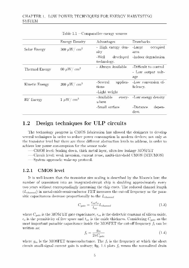
Table 1.1 Comparative energy sources
Energy Density Advantages Drawbacks
Solar Energy 500 µW/ cm2 - High energy den-sity
-Large occupiedarea
-Well developedtechnology.
-Indoor degradation
Thermal Energy 60 µW/ cm2 - Always Available -Dicult to control
- Low output volt-age
Kinetic Energy 200 µW/ cm3 -Several applica-tions
-Low conversion ef-ciency.
-Light weight
RF Energy 1 µW/ cm3 -Available every-where
-Low energy density
-Small surface -Distance depen-dent
1.2 Design techniques for ULP circuits
The technology progress in CMOS fabrication has allowed the designers to developseveral techniques in order to reduce power consumption in modern devices; not only atthe transistor level but there are three dierent abstraction levels to address, in order toachieve low power consumption for the sensor node:
CMOS level: Scaling down, thick metal layer, ultra-low leakage MOSFET Circuit level: weak inversion, current reuse, multi-threshold CMOS (MTCMOS) System approach: wake-up protocol.
1.2.1 CMOS level
It is well-known that the transistor size scaling is described by the Moore's law: thenumber of transistors into an integrated-circuit chip is doubling approximately everytwo years without correspondingly increasing the chip costs. The reduced channel length(Lchannel) in metal-oxide-semiconductor FET increases the cut-o frequency as the para-sitic capacitances decrease proportionally to the Lchannel
Cgate =εoxεotox
Lchannel (1.3)
where Cgate is the MOSFET gate capacitance, εox is the dielectric constant of silicon oxide,εo is the permitivity of free space and tox is the oxide thickness. Considering Cgate as themost important parasitic capacitance inside the MOSFET the cut-o frequency ft can bewritten as:
ft =gm
2πCgate(1.4)
where gm is the MOSFET transconductance. The ft is the frequency at which the shortcircuit small-signal current gain is unitary; g. 1.4 plots ft versus the normalized drain
5

CHAPTER 1. LOW POWER TECHNIQUES FOR ENERGY HARVESTINGSYSTEM
Figure 1.4 Cut-o Frequency trend in function of current density for dierent nodetechnology [WKvL+01]
source current density for ve technology nodes. RF circuits (Power amplier, Oscillator,Mixer,etc) take advantages from the MOSFET scaling because the transistor exhibitshigher current gain for the same operation frequency. Therefore same performances canbe achieved with less current and lower power consumption consequently.Also the threshold voltage decreases with the size downscaling, because the reduction inoxide thickness allows lower dierential potential needed to the MOSFET gate, in orderto create the conduction channel. As consequence, it is possible to decreases the supplyvoltage needed to put the transistors in saturated region. The main benet when thecircuit operates at lower power supply voltage is the reduction in active power dissipationPact for switched topology circuits. Pact is proportional to the square of supply voltageVDD, to the capacitors involved in charge and discharge operations and to the switchingfrequency fswitch:
Pact = CswitchV2DDfswitch (1.5)
It seems clear from eq. 1.5, that with the possibility to operate at lower VDD the powerconsumption decreases. However as the distance between drain-source is reduced and theoxide is thinner, the probability that an electron moves in transistor o-state is higherand thus the leakage current increases degrading the power consumption performance insleep mode; especially in ultra low duty-cycled system, where the circuit is o most of thetime, the leakage current impacts the power budget; ultra-low leakage MOSFET can helpwith reducing the o-state current.Moreover the higher chip cost in deeply scaling technology has to be considered especiallywhen low cost system is targeted.
Thick metal layer
Generally speaking the reduction of parasitic resistance allows to reduce the staticpower dissipation. This is the case for the drain source MOSFET resistance RDS in switch-ing circuit and also for the inductor and capacitor parasitic resistance. In energetic circuit
6

CHAPTER 1. LOW POWER TECHNIQUES FOR ENERGY HARVESTINGSYSTEM
Figure 1.5 Combinations to achieve 8 nH inductance [Van15] where W is the metalwidth and N is the numbers of turns.
(LC oscillator, tuned amplier, buck/bust voltage converter) the impact of lossy elementscan be traduced through the quality factor Q [Raz]
Q = 2πEnergyStored
EnergydissipatedperCycle(1.6)
High quality factor is preferable because the energy dissipated in lossy elements is low.A reduction in power consumption can be achieved by using high-Q elements and LCoscillator is a perfect example. In LC oscillator the oscillation is assured if the losses (theparasitic series resistances Rs of Inductor and Capacitor) are counterbalanced by an activeelement as the MOSFET transconductance gm.
gm ≥1
Rs
(1.7)
In rst approximation the gm is proportional to the drain-source current. Therefore forsmall value of parasitic resistance (high-Q) the gm needed is lower and the drain-sourcecurrent decreases proportionally. At low to medium frequency oscillation (from 400 MHzto 15 GHz) a customized inductor can helps in power consumption reduction with higherQ. In [Van15] thick metal and dense tapered spiral inductor shows quality factor improve-ments for 10 GHz frequency oscillation. Fig. 1.5 depicts dierent geometries to get 8 nHinductance with the highest Q at the same generated frequency.
1.2.2 Circuit Level
MOSFET operating region
Traditionally, the MOSFET is mostly used in strong inversion (SI) region with adrain-source current in the milli-Ampere range where the gate-source voltage Vgs has tobe greater than the threshold voltage Vth
Vgs >> Vth (1.8)
7

CHAPTER 1. LOW POWER TECHNIQUES FOR ENERGY HARVESTINGSYSTEM
In SI, for N-type Mosfet, IDS is proportional to the square of the eective gate-sourcevoltage
IDS =1
2
µnCoxn
W
L(Vgs − Vth)2 (1.9)
Where µ is the carrier velocity, Cox is the oxide capacitance, n is a slope factor, W andL are the width and the length of conduction channel. Only from the second half of90s [EV96], with the diusion of portable devices the weak inversion (WI) has been takenin consideration to address low power consumption in integrated circuit. In fact when Vgsis lower than Vth
Vgs << Vth (1.10)
the transistor operates in WI with an IDS in the range of micro-Ampere to the nano-Ampere. In this case the current is not more governed by a square law, but it follows anexponential behavior
IDS = 2nµCoxV2t
(W
L
)exp
(Vgs − VthnVt
)(1.11)
where Vt is the thermal voltage. However the passage from SI to WI is not abrupt andthe two regions are separated by the moderate inversion (MI), where Vgs diers aboveor below VTH to a few tens of mV. Therefore the three regions represent three dierentdegrees of MOS channel inversion. To give a coherent circuit design with the three levelof channel inversion the Inversion Coecient (IC) has been introduced, which allows acontinuous design ow from the WI to the SI. The IC [Bin07] can be found by the drain-source current, divided by the product of the shape factor S = W
Land the technology
current Io = 2nµCoxV2t
IC =IDSIoS
(1.12)
The IC ranges from 0.01 in WI to 100 in SI and the center value is 1 at the middle of MI.Therefore every value of IC corresponds to a precise level of inversion with a well denedbias point. The transistor width is calculated from the choice of the channel length L, thedrain-source current and the inversion coecient. Depending on the circuit performances,every operating region can accomplish a specic trade-o as shown in g. 1.6. Many works[EC15] [TSM15] [SH06] demonstrate that designing analog or radio-frequency circuits inMI ensures the best trade-o between power consumption, gm
Idseciency, low voltage design
and AC response.Fig. 1.7 shows a cascoded single stage Operational Transconductance Amplier OTAwhere the transistors operate in saturation region. When the MOSFET are biased at thelow side of SI (IC = 10) a Vds,sat = 0.24 V for each transistor can be assumed, whilewhen the low side of MI (IC = 0.1) is considered the Vds,sat = 0.12 V. The only parameteranalyzed is the minimum supply voltage needed to bias each transistor in saturation, andthe reduction of VDD,min is quite evident. The main drawback when MOSFET operatesin WI is the poor frequency response due to a large parasitic capacitance forced by thelarge MOSFET size. Moreover WI introduces a pronounce dependence en process andtemperature variations.
8

CHAPTER 1. LOW POWER TECHNIQUES FOR ENERGY HARVESTINGSYSTEM
Figure 1.6 Inversion coecient line number with voltage and shape factor MOSFETproperties [Bin07].
Current Reuse
The static power consumption in electronic circuit is given by the supply voltage VDDand the bias current Ibias owing from the supply voltage to the ground
Pstat = VDDIbias (1.13)
If two cascaded circuits (A and B) are considered (Fig. 1.8) the total power consumptionis equal to the sum of the single consumption:
Pstat,tot = Pstat,A + Pstat,B = VDD,AIbias,A + VDD,BIbias,B (1.14)
The Pstat,tot is reduced if the four variables are optimized. The main disadvantage isthat the generation of two separate supply voltages increases the system complexity andpower budget. In many case the chip size constraint and/or the energy available reducespace freedom degree in the design. Typically a single supply voltage is available for allcircuit blocks. Therefore the optimization, from the supply voltage point of view, cannotbe achieved completely and a lot of power is wasted. To overcome this problem and ifan adequate supply voltage is available, stacked structure can allow power consumptionreduction. In this case the bias current is recycled (reused) from the top circuit to thebottom one and the total power consumption is
Pstat,stack = VDD,stackIbias,stack (1.15)
The condition to achieve lower power consumption in stacked topology is VDD,stack =VDD,A = VDD,B and Ibias,stack = Ibias,A = Ibias,B. Moreover some precautions have to betaken against cross-talk phenomena, noise and high frequency loop. In [TSM15] a stackedLNA-VCO is presented, where each block achieves comparable performances with thestate of the art of stand alone circuit; a LC lter is inserted between the two circuits topresent high impedance at the frequency of interest avoiding cross-talk degradation.The reuse concept can be readapt to circuit level as in [?]. The RC relaxation oscillatorused to generate the time reference to the system is reused to implement reading-out cir-cuit for the measurement of the Relative Humidity. Therefore the oscillator accomplishestwo tasks saving power consumption and area occupied.
9

CHAPTER 1. LOW POWER TECHNIQUES FOR ENERGY HARVESTINGSYSTEM
Figure 1.7 Minimum supply voltage required in classical cascode OTA when the tran-sistors are biased in strong and in moderate inversion.
Multi-threshold CMOS
The leakage power consumption has become a serious problem in below 100 nm tech-nologies. In multi-threshold CMOS (MTCMOS) circuit, high-VTH transistors are used toblock the leakage path because of their low leakage current [SGMK15]. Basically it shuts-down a part of the circuit, disconnecting the main blocks from the power supply. Fig. 1.9illustrates a typical application where high threshold transistors cut-o the NAND logiccircuit. However this technique implies an increase in cost process due to an extra maskfor the two dierent threshold voltages. Moreover there is a trade-o between the size ofhigh-VTH transistor and the performances degradation of the main circuit.
10

CHAPTER 1. LOW POWER TECHNIQUES FOR ENERGY HARVESTINGSYSTEM
Figure 1.8 Cascaded circuit block with two separate supply voltage and independentbias currents.
Figure 1.9 Multi-threshold application in logic circuit.
1.2.3 System level
Wake-up scheme and duty-cycled radio
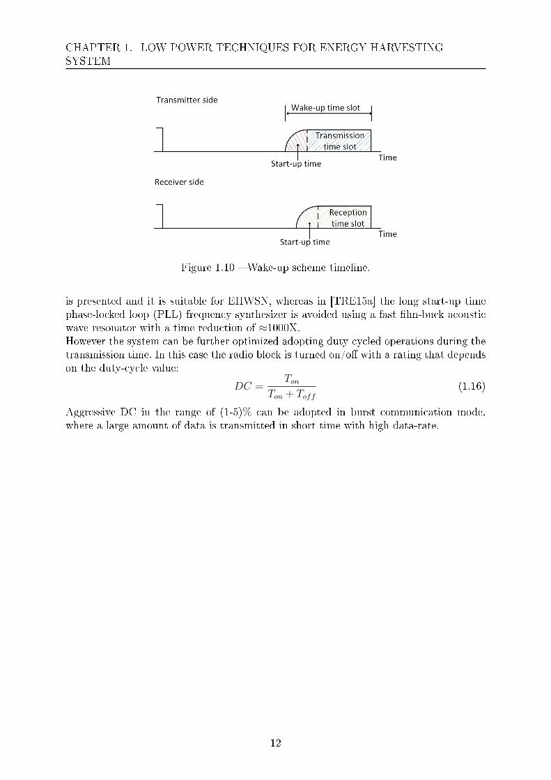
As it will be described in the next chapters the most hungry part in wireless sensor nodeis the transceiver circuit. A large number of papers suggest to keep the nodes transmitterpart in low-power sleep mode for most of the time, allowing the node to operate at highestpower consumption level only for a very short time. Wake-up scheme is a largely adoptedtechnique to reduce the energy consumption extending the sensor node lifetime. Fig. 1.10depicts the time-slot division for waked-up sensor node. The active time-slot includes:
start-up time where auxiliary circuits generate the wake-up signal for the trans-mission/reception part. After the radio-frequency circuits need a settling time toachieve proper operation (especially for the frequency synthesizer).
transmission/reception time where the communication between the sensor nodeeectively takes place.
To reduce the required overall energy both start-up and transmission slots have to be asshort as possible for a lower power consumption. In [JLBS15] a 5.8 nW wake-up timer
11
CHAPTER 1. LOW POWER TECHNIQUES FOR ENERGY HARVESTINGSYSTEM
Figure 1.10 Wake-up scheme timeline.
is presented and it is suitable for EHWSN, whereas in [TRE15a] the long start-up timephase-locked loop (PLL) frequency synthesizer is avoided using a fast lm-buck acousticwave resonator with a time reduction of ≈1000X.However the system can be further optimized adopting duty-cycled operations during thetransmission time. In this case the radio block is turned on/o with a rating that dependson the duty-cycle value:
DC =Ton
Ton + Toff(1.16)
Aggressive DC in the range of (1-5)% can be adopted in burst communication mode,where a large amount of data is transmitted in short time with high data-rate.
12

CHAPTER 1. LOW POWER TECHNIQUES FOR ENERGY HARVESTINGSYSTEM
1.2.4 Conclusion
In this chapter a description of the dierent energy harvesting sources usable forsmall scale applications has been presented. The low energy density available and thehigh variability pose a big challenge for the designers. Low-power design techniques aremandatory to extend the devices lifetime. The second part of chapter has described thesetechniques highlighting the advantages and the drawbacks.The three level of optimization, transistor, circuit and system, can be combined to achievethe best trade-o between the performances and the power consumption. In the nextchapters a system overview and a design ow for very ecient voltage regulator andultra-low power transmitter are presented.
13

Chapter 2
System Approach
The technology progress occurred in the last ten years in highly integrated microelec-tronic circuits, sensors, actuators, and wireless communications technology allowed thedissemination of wireless sensor network (WSN) in several domains:
Environmental Monitoring
WSN can be used for forest surveillance, weather forecasting. It is a natural can-didate, because the variables to be monitored are usually distributed over a largearea. In addition WSN can facilitate the measurement of a large variety of envi-ronmental data for a huge number of applications such as agriculture, meteorology,geology, zoology, etc.
Health monitoring
WSN could potentially provide better health-care delivery. They could improvethe interaction between the patient and the medical sta. Several physiologicalparameters can be monitored, as (hearth condition, blood pressure, blood glucose,organ monitor, cancer detector). When the sensors are implanted for healthcarepurpose, they are called Body Sensor Network (BSN).
Industrial Sensing
The industrial sector is one of the most involved player for the development ofWSN. With the possibility to acquire information in real-time, unexpected failurescan be avoided improving production quality and reducing costs. One of the mainuse is in the food industry to monitor the food supply chain.
Home Security
Domestic represents another potential area for WSN. The "smart home" can regu-late the room temperature, control air quality, adjusting lighting. Sensor networkscan also improve the security of the house by sending an alarm message to the res-ident when it detects intruders, gas leakage, re occurrence or other safety risks.
WSN can generally be described as a network of nodes that cooperatively sense andmay control the environment enabling interaction between persons or computers and thesurrounding environment. In spite of their versatility, the main constraint is the energyneeded for the operation, specially when WSN are deployed in hostile environment or overa large area making the battery replacement very dicult, expensive or even impossible.For example, the study carried-out in [KBA16] shows the battery duration for WSNswith ZigBee/IEEE 802.l5.4 protocol. This standard has been developed by the Institute ofElectronic and Electrical Engineer (IEEE) for low-power, low data-rate wireless personalsensor networks (WPSNs). The most adopted transmission frequency is 2.4 GHz with
14
CHAPTER 2. SYSTEM APPROACH
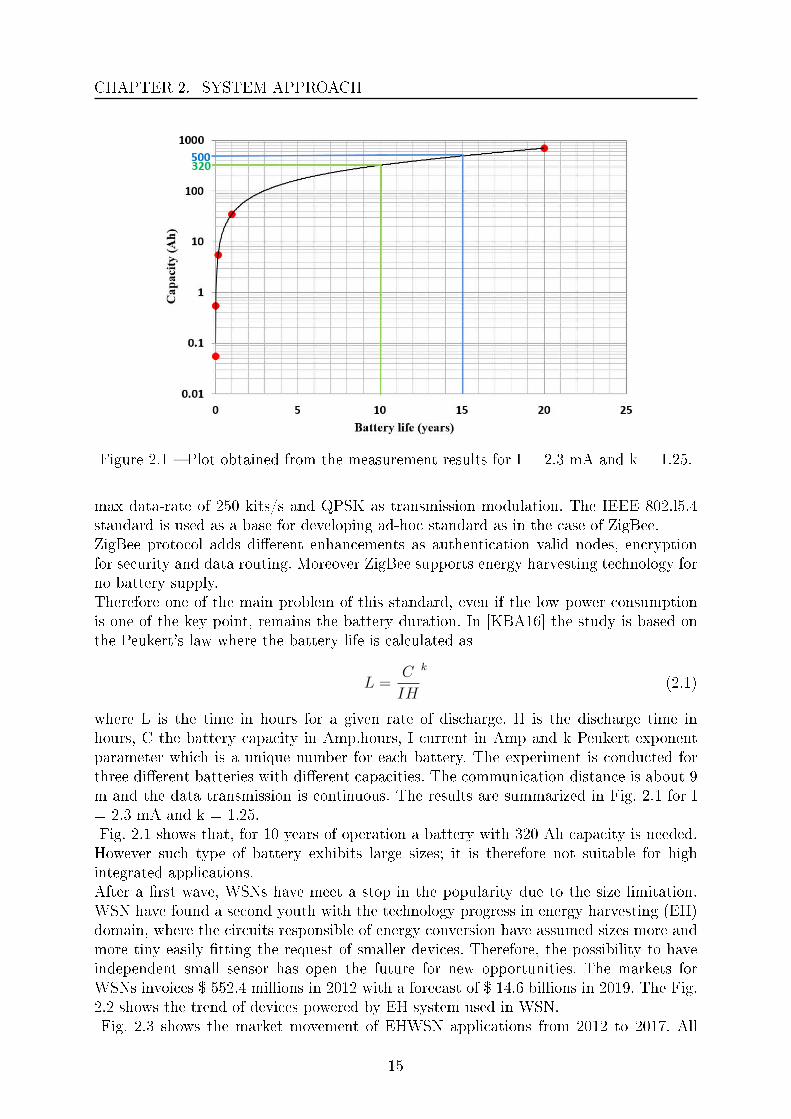
Figure 2.1 Plot obtained from the measurement results for I = 2.3 mA and k = 1.25.
max data-rate of 250 kits/s and QPSK as transmission modulation. The IEEE 802.l5.4standard is used as a base for developing ad-hoc standard as in the case of ZigBee.ZigBee protocol adds dierent enhancements as authentication valid nodes, encryptionfor security and data routing. Moreover ZigBee supports energy harvesting technology forno battery supply.Therefore one of the main problem of this standard, even if the low power consumptionis one of the key point, remains the battery duration. In [KBA16] the study is based onthe Peukert's law where the battery life is calculated as
L =C
IH
k
(2.1)
where L is the time in hours for a given rate of discharge, H is the discharge time inhours, C the battery capacity in Amp.hours, I current in Amp and k Peukert exponentparameter which is a unique number for each battery. The experiment is conducted forthree dierent batteries with dierent capacities. The communication distance is about 9m and the data transmission is continuous. The results are summarized in Fig. 2.1 for I= 2.3 mA and k = 1.25.Fig. 2.1 shows that, for 10 years of operation a battery with 320 Ah capacity is needed.However such type of battery exhibits large sizes; it is therefore not suitable for highintegrated applications.After a rst wave, WSNs have meet a stop in the popularity due to the size limitation.WSN have found a second youth with the technology progress in energy harvesting (EH)domain, where the circuits responsible of energy conversion have assumed sizes more andmore tiny easily tting the request of smaller devices. Therefore, the possibility to haveindependent small sensor has open the future for new opportunities. The markets forWSNs invoices $ 552.4 millions in 2012 with a forecast of $ 14.6 billions in 2019. The Fig.2.2 shows the trend of devices powered by EH system used in WSN.Fig. 2.3 shows the market movement of EHWSN applications from 2012 to 2017. All
15

CHAPTER 2. SYSTEM APPROACH
Figure 2.2 Market forecast for EH devices used in WSN applications.
sectors exhibit an growth in the number of employed devices.To make a sensor networks adaptable for a wide range of applications, the following
requirements should be addressed: Low Cost: The utility and scalability of a WSN highly depend on its density,
which means large number of sensor nodes in the assignment area. To make theinstallation cost eective, the cost of individual sensor node should be extremelylow.
Low Power: Nodes must be able to ensure a permanent connectivity and coveragefor long periods, up to 10-20 years, without service interruption. Low power con-sumption represents one of the main challenge in modern devices, and it is of greatimportance when the sensor is supplied by low density energy source.
Small Size: WSNs are desired to replace cables that are often impracticable. There-fore, the size of the sensor node must be small enough in order to allow the WSNsto monitor the environment in a discreet and transparent manner.
However nowadays as introduced in the Chapter 1, the energy available from theharvesting transformation is not sucient to power the sensor node in continuous modeoperation. For example the harvested power from vibration in industrial application caneasily achieve 100 µW/cm2 [RM10], but modern sensor node in transmission mode requiresabout 5 to 10 mW depending on the application. Fig. 2.4 shows that if one hand WSNrequires less power thanks to development technological, on the other hand high ecientharvesting circuits allow to maximize the low energy available from the environmentalsources.
However until now, technologies limitation (for example leakage current, process de-viations) and performance constrains (noise, PVT variations) prevent the two curves toreach a intersection point. Actually a continuous autonomous operations can not be there-fore assured. The sensing and data communication reliability can be assured only if sensornode operates for a fraction of total time. Therefore the two curves can approach, becausemicro-watt power availability is able to sustain operations in the range of mW. The build-ing block diagram of an EH sensor node is shown in the Fig. 2.5
16

CHAPTER 2. SYSTEM APPROACH
(a)
(b)
Figure 2.3 Energy Harvesting WSN market in 2012 (a) and prevision of market in 2017(b)
17

CHAPTER 2. SYSTEM APPROACH
Figure 2.4 Power comparison between WSN and Energy Harvested circuit.
The electrical energy coming from the harvest transformation can be used to directly sup-ply the sensor node or stored into a supercapacitor or a rechargeable battery. Althoughin some applications it is possible to bypass the energy storage, in most of the case thestorage component acts as an energy buer for the system, with the main purpose ofaccumulating and preserving the energy.In order to manage the energy available from the storage element, the power manage-ment unit (PMU) has to be designed to extend the sensor lifetime. It controls the levelof stored energy and at the demand of power depending on the adopted protocol, it sup-plies the sensor and/or the other circuits. The environmental information sensed is thentransformed into digital information by the ADC and stored in the memory. In generalthe sensing and the data transmission are not accomplished at the same time, becausethe transmitter is the main power hungry block and the energy available is not enough toguarantee the two operations at the same time.Finally the data transmission can be validated internally by the PMU or externally ondemand by the users.
18

CHAPTER 2. SYSTEM APPROACH
Figure 2.5 Architecure of energy harvesting sensor node.
2.1 Energy Management
The purpose of this work is to design low-power circuits for RF-energy harvestingWSN. In particular low drop-out voltage regulator and transmitter block have been de-signed. A framework at the system level can facilitate the circuit design.As briey introduced an energy buer (rechargeable battery or super-capacitor) is manda-tory for duty-cycled power manager to stock the energy when the system is in idle modeand then make it available when requested. A simple PMU introduced in [PCFP14] isdepicted in Fig.2.6. To supply the regulated voltage to the RF front-end blocks, PMUuses dierent circuits to manage the stored energy.Voltage limiter is used to limit the maximum voltage with a safe margin.The voltage sensor veries that the voltage across the capacitor is between two denedbends Vlow and Vhigh.When the voltage stored into the capacitor reaches Vlow, the PMU turns-o the voltageregulator and the system is in idle mode. During the idle mode the PMU draws a littlebias current due to the monitoring circuits that are continuously on to ensure properoperation. When the voltage capacitor reaches Vhigh, the PMU turns on the voltage regu-lator, the current ows from the capacitor to the voltage regulator output and the sensingoperation and data transmission can take place.It seems clear that in the case of linear voltage regulator, where the regulated outputvoltage is obtained "loosing" a part of input voltage over a variable resistor, the stablePMU output voltage Vreg has to respect the following condition
Vreg < Vlow < Vhigh (2.2)
where Vreg depends on the application specications (transmission distance, quality andspeed of transmission) and on the circuit architecture (stacked topologies, technology re-liability), Vlow depends on the voltage regulator performances and on the minimum inputvoltage for which the regulation is ensured, Vhigh can be obtained by the system energyanalysis. Fig. 2.7 shows the energy prole (top gure) of harvesting sensor node where the
19

CHAPTER 2. SYSTEM APPROACH
Figure 2.6 Power management transistor level schematic implemented in [PCFP14]
transmission time ton is less than the idle time toff . In this case high power hungry circuitsas frequency synthesizer and power amplier can be sustained by low power source as RFenergy harvesting. The bottom graph in Fig. 2.7 shows the transient of voltage storedin the capacitor and the voltage at the regulator output. During toff the sensor node isin harvesting mode and the capacitor is charging. The charging time depends on sourcesignal quality. During this time interval the energy cost of monitor circuits has to be verylow in such way to preserve the capacitor charge.
20

CHAPTER 2. SYSTEM APPROACH
Figure 2.7 The top graph depicts an example of energy prole in harvesting system.In the bottom graph the trend of voltage stored into the capacitor (red line) and theregulated voltage at the output of the PMU.
The energy stored in the capacitor C is given by
EC =
∫ Qf
Qi
Q
Cdq =
1
2C(Q2
f −Q2i ) (2.3)
where Qf is the charge stored at Vhigh and Qi is the charge stored at Vlow. The energystored in the capacitor can be rearranged as
EC =C
2(V 2
high − V 2low) (2.4)
The energy needed for the data communication, assuming OOK modulation scheme forthe transmission circuit (PA,VCO), and continuous operation during modulation for theother circuits to reduce start-up time can be written as
Etransmission = ETX + Ereg = (pPDC,TX + PDC,system)ton + (IloadVdrop)ton (2.5)
21
CHAPTER 2. SYSTEM APPROACH
The above equation is obtained assuming the following hypothesis : The transmitter block is responsible of the DC power consumed PDC,TX modulated
by the probability p to transmitting a '0' or '1' data bit. PDC,system includes the DC power consumed by the control circuits As it will be explained in the next chapter, a linear voltage regulator has been
chosen to transform the unregulated input voltage to the regulated output one.The power dissipated by the voltage regulator is mainly due to the voltage droppedacross the pass element Vdrop and to the load current Iload that ows from theinput to the output. As Iload is quite high, due to the bias current drawn by thetransmitter, the energy required by the regulator can not be neglected.
Surely the energy required by the transmission block has to be equal to the energy storedin the capacitor
Etransmission = EC (2.6)
therefore from the upper equation is possible to nd the storage voltage Vhigh
Vhigh =
√2tonC
(pPDC,TX + PDC,system + IloadVdrop) + V 2low (2.7)
Observing the above equation Vhigh relies on dierent parameters: the size of the storagecapacitor C, the power consumed by the transmitter, the type of modulation and alsothe amount of data to be transmitted. Indeed ton is obtained by the ratio between thedata packet length and data-rate. It is interesting to note that Vhigh value impacts theregulator energy eciency. Without entering into detail,because voltage regulator is thesubject of the next chapter, the energy eciency can be writen as
ηenergy =VregIloadtonVinIloadton
=VregVin
(2.8)
Vin is not xed but decreases from Vhigh to Vlow. The above equation states that the threevoltage values Vreg, Vhigh and Vlow have to be as close as possible in order to not deterioratethe regulator eciency.
2.2 Link budget, data rate and duty cycle.
2.2.1 Required link Budget
Generally the power consumed by the power amplier (PA) to cover a given distance isthe main contribution to the power dissipated by the transmitter block. Outdoor sensorsare generally 100 m spaced-out and the communication is almost free of obstacles. On theother hand, in indoor network the transmission antenna has to cover a range about of 5-10m and the signal quality could be degraded by walls. Dierent is the situation for BWNswhere the distance does not exceed 1 m. The PA DC power is strictly dependent on theRF output power level needed for the applications. The rst step in the transmitter designconcerns the estimation of the power radiated Prad at the PA output. At rst glance, therequired Prad can be obtained as follow:
Prad = PRX −Gantenna − PL = PRX −Gantenna − 20 log
(λ
4πD
)(2.9)
22

CHAPTER 2. SYSTEM APPROACH
where PRX is the receiver sensitivity, Gantenna is the antenna gain, λ is the wave length forthe carrier frequency and D is the communication distance. The gain of a typical surfacemount antenna can be estimated at 0 dB for a frequency carrier of 2.4 GHz while thepath loss (PL) terms in free space can vary between -22dB to -30dB for a distance Dbetween 1m to 10m. The last term in the right side of the eq. 2.9 PRX is almost dicultto calculate [Ben09] because it relies on several variables:
PRX,dBm = Nin +NF + 10 log(B) + (PredictedS
N) => PRX,linear = Nin ×NF ×B ×
S
N(2.10)
where Nin represents the input noise density originated on the source resistance for exam-ple antenna equivalent resistor. Nin = -174 dBm/Hz is considered for a perfect receiver atroom temperature having a bandwidth of 1 Hz (no internal noise and ability to operatewith a signal having the same power as the input noise).B is the bandwidth of the receiver signal and S
Nis the signal to noise ratio and can be
specied to attain a given BER (bit error rate), depending on the adopted modulationscheme.The receiver noise gure NF is the dierence between the input S
Nand the output S
Nand
it gives an information about the noise generated by the receiver circuit blocks.To give an order of magnitude about the receiver sensitivity the Tab 2.1 shows the receiverState of the Art for ultra-low power application.
Table 2.1 Comparative ULP receiver
[VHH+11a] [LBvdH+14][OST+16] [LBW+15] [PPA+15]
Data-rate 5Mbps 2Mbps 1Mbps 250kbps 250Kbps
Modulation OOK HS-OQPSK
GFSK - -
Topology Super Reg. SIF-PDC HybridLoop
- -
Pdiss (mW) 0.534 2.4 6 3.3 11.2
PRX (dBm) -75 -92 -90 -94 -94.5
Evaluating the data reported in the previous table an average value of -92 dBm canbe considered for ULP receiver. Therefore the minimum Prad in the case of 2.4 GHzsignal carrier, for an average communication distance D of 5 m has to be equal to -38dBm. To cover a shorter distance of 1 m the Prad decreases to about -50 dBm. Howeverthese are optimistic values, because estimated with the transmission occurring under idealconditions. To overcome sudden variations, 30 dB of path loss should be added for safemargin. An ULP transmitter with an average transmitter power of -15 dBm is considered.To give an idea about the power consumption of a transmitter, it is possible to assumethat the PA is the most power hungry circuit. Therefore the DC power required for agiven Prad in the case of class-A topology is:
PDC =2V 2
DD
RL
(2.11)
23

CHAPTER 2. SYSTEM APPROACH
Figure 2.8 Wireless sensor network mesh architecture
PDC = 40 mW is dissipated to transmit -15 dBm with a supply voltage of VDD = 1 Vdelivered on a 50 Ω output resistance RL.The energy required to transmit n-bit length data depends on the performances of thereceiver. High sensitivity demands indeed high receiver power consumption but lowertransmitter consumption.A typical sensor node is equipped with a radio block for transmission and receptionoperation. For example, in mesh networks (g. 2.8) the message is propagated along a pathby hopping from node to node until it reaches its destination. Optimizing both receiverand transmitter can represent an hard task in energy harvesting environment, becauselowering the power radiated surely means lower power consumption for the transmittercircuits but, on the other side, the receiver needs high sensitivity to decrease error bitratio and this increases its power consumption. The same trade-o occurs when lowersensitivity is accepted, because of the increased radiated power.To alleviate the sensor node complexity and to separate the trade-o between radiatedpower and receiver sensitivity, a centralized network (g. 2.9) can be adopted, where thedata message passes from the sensor to the HUB in an unidirectional way. Thereforethe sensor nodes are equipped only with the transmission block and they are powered byharvesting source. The HUB can perform both operation, transmission and reception, withhigh performances because it is equipped with a large capacity battery. The transmitter insensor node can be optimized under a power consumption point of view, since the receivercan achieve high performances and complexity.In any case to extend the network lifetime the energy required by the transceiver toprocess the incoming signal has to be limited. A rendez-vous scheme based on pseudo-asynchronous protocol is possible to adopt where the data transmission is accomplished ondemand, using a periodic wakeup scheme. In [LRWW05] is demonstrated that Receiver-Initiated Cycled Receiver (RICeR) outperforms low power consumption when comparedto Transmitter-Initiated Cycled Receiver (TICeR). In RICeR the destination node has thetask to initiate the packet exchanges. Basically the data transmission is done as followg.2.10:
24
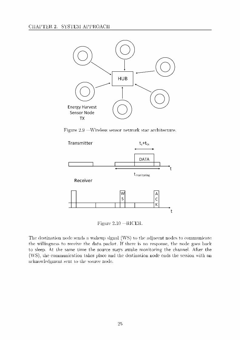
CHAPTER 2. SYSTEM APPROACH
Figure 2.9 Wireless sensor network star architecture.
Figure 2.10 RICER.
The destination node sends a wakeup signal (WS) to the adjacent nodes to communicatethe willingness to receive the data packet. If there is no response, the node goes backto sleep. At the same time the source stays awake monitoring the channel. After the(WS), the communication takes place and the destination node ends the session with anacknowledgment sent to the source node.
25

CHAPTER 2. SYSTEM APPROACH
2.2.2 Data Rate and Duty Cycle Trade-o.
In transmission system, data-rate (DR) is the rate at which the data informationsare transmitted. Considering the bandwidth allocation the Shannon's theorem gives thepossibility to calculate the channel capacity C (the maximum rate at which the data canbe transmitted over given communication path and under given condition )
C < B log2
(1 +
S
N
)(2.12)
Where B is the channel bandwidth and SNis the signal to noise ratio specication.
For short range devices the Electronic Communication Committee (ECC) has establishedthe ERC recommendation [ECC17] for each frequency band and for dierent applications.For tracking, tracing and data acquisition in sensors and actuators applications, medicalbody area network system, wireless industrial application in the frequency band 2483.5-2500 MHz for 1 mW max output power radiated the maximum occupied bandwidth hasto be less than 3 MHz.Therefore the channel capacity using the Eq. 2.12 is equal to 10 Mbps for 10 dB of signalnoise ratio. As the DR states the TX payload, it is understandable that for a given numberof bits Nb higher DR means shorter transmission time. Therefore it is possible to expressthe energy needed to transmit a string of n bits as
Eb =
[PBB +
Pradη
] [Nb
DR
]=
[PBB +
PRXη ×Gantennna × PL
] [Nb
DR
](2.13)
where PBB is the power dissipated by the baseband circuits, η is power eciency which isequal to the ratio of Prad and the DC power dissipated by the TX circuits PDC,TX . The Ebstated in the eq. 2.13 is low limited due to some trades-o between the variables involvedin the equation.
The baseband power consumption is limited due to the noise performance andPVT (Process Variation Temperature) as the weak inversion region is exploited forthe Mosfet transistors.
High Power eciency requires high radiated power, but it is not the case in shortdistance communication where Prad ≈ 100 µW. As it will be demonstrated inchapter 4, designing a transmitter block with the same power consumption is avery hard task.
At rst glance it seems that high data rate reduces the required energy [DvdZBK11][ESY05]. This is true until the power consumption due to the higher frequencyoperations does not increase excessively. Moreover the noise bandwidth increasesaccordingly and better sensitivity is required for the same bit error rate.
By introducing the spectral eciency ηDR−BW , as the ratio between DR and B
ηDR−BW =DR
B(2.14)
Therefore expressing the PRX in linear value, the eq. 2.13 can be rearranged as
Eb =
[PBB +
Nin ×NF ×DR× SN
η ×Gantenna × PL× ηDR−BW
][Nb
DR
](2.15)
26

CHAPTER 2. SYSTEM APPROACH
The results obtained is derived for continuously operation. However, intuitively andas largely reported in literature, the sensor node lifetime is extended when a duty-cycleprotocol is adopted. Duty Cycle is the ratio between the slot-time when the sensor is onand the total time. This technique allows to preserve energy, because in o mode the nodeburns very low power in comparison with the on mode.Following the indication in [TRE15a] the duty cycle DC can be calculated as
DC =DRA
DR(2.16)
where DRA is the application data rate and DR is the data rate achievable by the system.By obtaining the DR in function of the DC and DRA, substituting it into eq. 2.15 andconsidering the carrier generation circuits start-up as in g. 2.10 the energy required totransmit n bit is equal to:
Eb =
[PBB +
Nin ×NF ×DRA× ηDR−BW × SN
η ×Gantenna × PL×DC
] [Nb ×DCDRA
+ ts
](2.17)
The above equations states that an aggressive DC, up to 5%, do not allows a reductionin the required energy per bit because it is present at the numerator and denominator inthe right side of the equation. Moreover the choice of low or high value aects the powerconsumption in both receiver and transmitter part. In wake-up scheme both transmitterand receiver have to be turn-on and turn-o periodically, therefore to achieve low DCthe two circuits the start-up time has to be reduced consequently. A quick response isobtained with an increase in the power consumption and observing the eq. 2.17 it is clearits no-monotonic trend with the duty-cycle. Generally speaking aggressive DC requireshigher power consumption.Therefore it is possible from the eq. 2.17 to calculate the optimum DC for which theenergy required is minimum.
δEbδDC
= 0 => DCopt =
√Nin ×NF × ηDR−BW × ts ×DRA× S
N
η ×Gantenna × PL× PBB ×Nb
(2.18)
The optimum duty-cycle relies on several parameters and there are some constraints whichimpose the boundaries for the choice of the duty-cycle. For the example Gantenna increaseswith the sphere radius that completely contains the antenna and the small size demandedto the sensor node limits the maximum antenna gain consequently. Processing longerbit string increases the circuit complexity and it aects other system performances assignal-to-noise ratio, the noise gure and the bandwidth eciency.
27
CHAPTER 2. SYSTEM APPROACH
2.2.3 Conclusions
An overview has been given of WSN and physical layer node. Moreover the energyconstraints have been shown and also the techniques and the circuit performances thathave to be considered to extend the node lifetimes have been detailed.The relation between the maximum and minimum stored voltages into the capacitor andthe regulated voltage have been introduced considering the voltage regulator energy e-ciency.As concern the transmit section, the indication about the link budget has been given andthe trade-o between the receiver sensitivity and data rate has been explained. Duty-cycleoperation shows that to be a powerful technique to reduce the energy cost for transmit-ted data. Optimum Duty-Cycle value permits to reduce as much as possible the requiredenergy per bit.The results obtained in this chapter are used to properly design high about the perfor-mances for voltage regulator and transmitter.
28

Chapter 3
Voltage Regulator
In RF energy harvesting system, the DC voltage obtained from the AC-DC conversionof the incoming signal suers from the variability of the wireless power transfer itself. Tosmooth these uctuations a voltage regulator is mandatory to deliver a clean voltage fordelicate circuit blocks as: ADC, VCO, etc. As explained in the previous chapter, the lowenergy available imposes dierent challenges in terms of performances for every involvedcircuit. This chapter describes the design methodology of ULP low drop-out (LDO) voltageregulator with good regulation performances while keeping high power eciency.The rst part of the chapter provides an overview on the main characteristics of thevoltage regulator and the comparison between the two topologies of regulation: switchingand linear. The reasons of choice are also illustrated. The chapter then ends by describingthe design methodology of the LDO regulator with the simulation results.
3.1 Background
In modern devices, the energy management and the power delivery have assumed acrucial role. Optimizing the use of the energy contained in a battery or in other storagedevice, for example super-capacitor as in the case of harvesting source, allows to extendthe autonomy of the device. The power management unit (PMU) Fig. 3.1 is responsiblefor a balanced distribution of energy according to the circuits consumption and the stateof operations.
Figure 3.1 Power Management Unit
29

CHAPTER 3. VOLTAGE REGULATOR
The eciency of harvesting systems strongly depends on the optimization of the powermanagement unit. Due to the energy constraint, only by means of a depth understandingof the application it is possible to make the correct choices in terms of architecture andperformances. For example in a body area network application (BAN), the sensor andthe transmission block have to turn-on frequently to monitor the vital parameters for ashort time period with very short distance (< 10 cm); while in wireless sensor applica-tion (WSN) where the distance is more important (> 1 m), the transmission time hasto take a longer duration to prevent false data transmission due to channel interference.It is clear that the two applications are dierent in terms of data-rate, frequency mod-ulation, duty-cycle and power consumption. For example in [MBT+13] the PMU has tomanage two dierent duty-cycled signals, in order to power supply or not the sensor andUWB transmitter, saving the power consumption. Typically the power management unitdirectly interfaces with the load through the voltage regulator. In most of case, the reg-ulation performances dictate the design specications of the PMU (output voltage, max.supply current, transient response, etc). The following section describes the two dierentmethodologies of regulation illustrating the advantages and the drawbacks for each ofthem.
3.2 Voltage Regulator
Voltage regulator is a circuit that converts an unregulated DC input voltage into astable and clean DC output voltage. A stable and clean voltage at the output terminals isdesired, in order to not deteriorate the performances of the load circuits. It is composedof two main parts as depicted in Fig. 3.2
1. the conversion stage transforms the unregulated input voltage to a regulated outputone.
2. the control feedback monitors the output voltage and tunes the conversion stagecondition in order to keep the output voltage at the nominal value
Evaluating the static and dynamic characteristics, not only permits to compare the dif-ferent topologies but also to understand the performances to improve which best matchwith the targeted application.
Figure 3.2 General block diagram of voltage regulator
30

CHAPTER 3. VOLTAGE REGULATOR
3.2.1 Static Characteristics
The static characteristics are evaluated under steady-state conditions when all thetransient phenomena are clearly completed. They dier for the DC or AC nature.
Eciency
In energy harvesting system the eciency is one if not the most important design criterionto evaluate. It gives the power cost of the transformation, in other words the amount ofpower loss in the circuit. The eciency is expressed as the ratio between the deliveredoutput Pout and the input power Pin :
η =PoutPin
(3.1)
An eciency of 100% means no power loss. But with real components the power isdissipated in resistive part or in other way as leakage phenomena.
Power Density
The power density puts in relation the eciency with the area occupied by the chip. It isexpressed as Pout normalized to the total area A:
PD =PoutA
(3.2)
Load Regulation
The load regulation describes the variations of the steady-state output voltage whenoutput current ILOAD changes (Fig. 3.3)
Figure 3.3 Load Regulation
As the load regulation is not linear for the entire load range, it is measured for theminimum and maximum value
31

CHAPTER 3. VOLTAGE REGULATOR
LoadRegulation =Vout1 − Vout2Iout1 − Iout2
=ROL
1 + AolβFB(3.3)
where ROL is the open loop output resistance, Aol the open-loop gain and βFB thefeedback factor of the regulator. Vout1 and Vout2 are the boundaries of output voltages con-sidered and Iout1 and Iout2 the respective output currents. The load regulation is relatedto the open loop gain of the converter. So higher open-loop gain is preferred to assure abetter regulation.
Line Regulation
The line regulation describes the variations of the steady-state output voltage for a vari-ation of the input voltage Vin (Fig.3.4)
Figure 3.4 Line Regulation
It is measured for the minimum and maximum value of unregulated input voltage
LineRegulation =Vout1 − Vout2Vin1 − Vin2
≈ 1
1 + βFBAol(3.4)
Where Aol is the open loop gain and βFB is the feedback factor. So line regulation isimproved by high open-loop gain.
Noise
The noise is an AC characteristic and it quanties two aspects of the regulator: 1) thecapability to suppress the interferences coming from the input signal; 2) the inherent noiseproduced by the regulator itself. The noise performances are evaluated with power supplyrejection ratio PSR.
3.2.2 Dynamic Characteristics
The dynamic characteristics exhibits the capability of the regulator to restore the out-put voltage when a transient event appears.
32
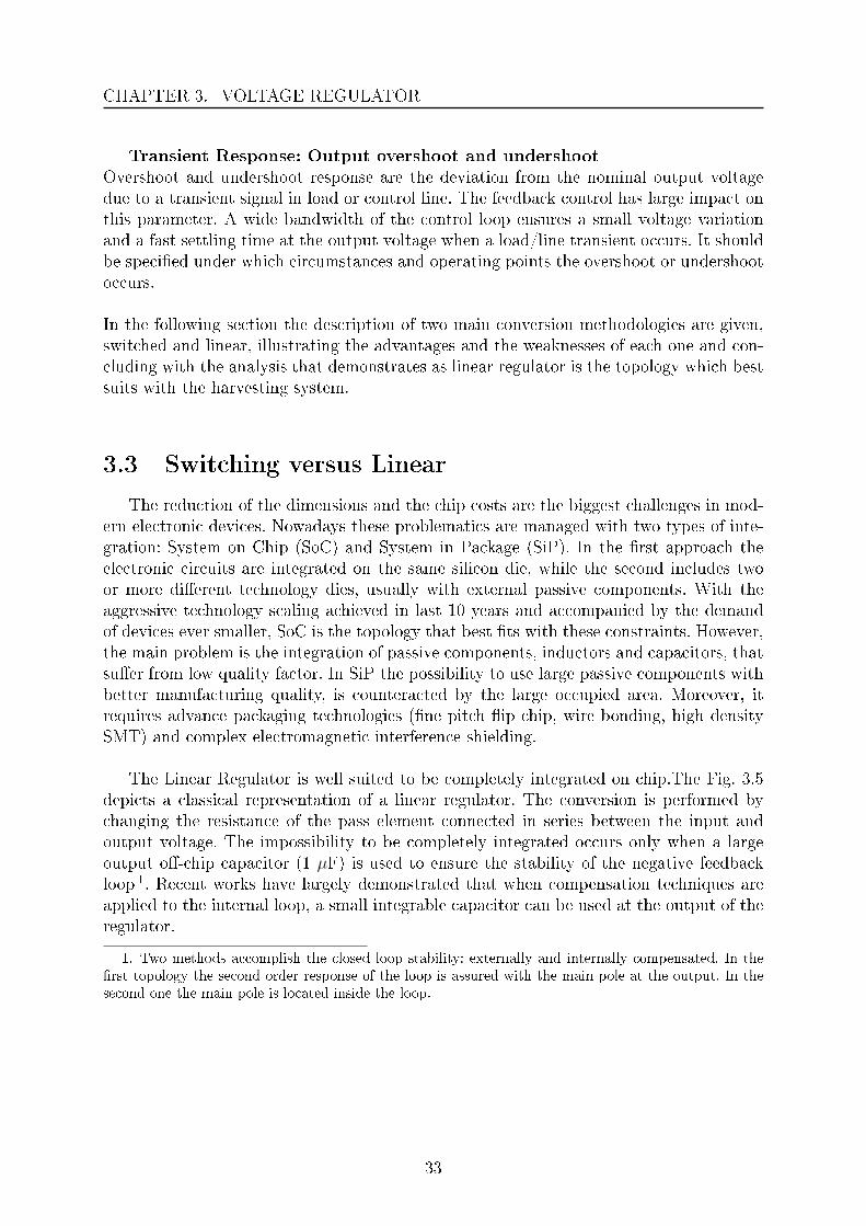
CHAPTER 3. VOLTAGE REGULATOR
Transient Response: Output overshoot and undershoot
Overshoot and undershoot response are the deviation from the nominal output voltagedue to a transient signal in load or control line. The feedback control has large impact onthis parameter. A wide bandwidth of the control loop ensures a small voltage variationand a fast settling time at the output voltage when a load/line transient occurs. It shouldbe specied under which circumstances and operating points the overshoot or undershootoccurs.
In the following section the description of two main conversion methodologies are given,switched and linear, illustrating the advantages and the weaknesses of each one and con-cluding with the analysis that demonstrates as linear regulator is the topology which bestsuits with the harvesting system.
3.3 Switching versus Linear
The reduction of the dimensions and the chip costs are the biggest challenges in mod-ern electronic devices. Nowadays these problematics are managed with two types of inte-gration: System on Chip (SoC) and System in Package (SiP). In the rst approach theelectronic circuits are integrated on the same silicon die, while the second includes twoor more dierent technology dies, usually with external passive components. With theaggressive technology scaling achieved in last 10 years and accompanied by the demandof devices ever smaller, SoC is the topology that best ts with these constraints. However,the main problem is the integration of passive components, inductors and capacitors, thatsuer from low quality factor. In SiP the possibility to use large passive components withbetter manufacturing quality, is counteracted by the large occupied area. Moreover, itrequires advance packaging technologies (ne pitch ip chip, wire bonding, high densitySMT) and complex electromagnetic interference shielding.
The Linear Regulator is well suited to be completely integrated on chip.The Fig. 3.5depicts a classical representation of a linear regulator. The conversion is performed bychanging the resistance of the pass element connected in series between the input andoutput voltage. The impossibility to be completely integrated occurs only when a largeoutput o-chip capacitor (1 µF) is used to ensure the stability of the negative feedbackloop 1. Recent works have largely demonstrated that when compensation techniques areapplied to the internal loop, a small integrable capacitor can be used at the output of theregulator.
1. Two methods accomplish the closed loop stability: externally and internally compensated. In the
rst topology the second order response of the loop is assured with the main pole at the output. In the
second one the main pole is located inside the loop.
33

CHAPTER 3. VOLTAGE REGULATOR
Figure 3.5 Linear Regulator
For example, only 5 pF compensation capacitor with a cascode current compensationstage to achieve the stability is needed [LGZ+15]. Q-reduction circuit proposed in [LML07]permits to minimize on-chip capacitor (7 pF) and quiescent current. One of the main lim-its is that only down-conversion is possible, given that the output voltage is the dierencebetween the input voltage and the voltage drop over the pass element. Due to the con-tinuous linear control and the fact that the conversion is performed dissipating the poweron the pass element, the power eciency is not one of the strengths of this topology.Analyzing the eciency equation:
η =VoutILoad
(ILoad + Iq)Vin(3.5)
where Iq is the total drawn current to the ground, it is not preferable to have largeconversion ratio Vout
Vinas anticipated in chapter two. If the quiescent current is negligible
respects to the output current, it is clear that transforming 3 V into 1.5 V for example,the maximum eciency is only 50%. While the unregulated voltage is about 1.8 V theeciency increases to 83 %. For this reason linear regulator is preferable when the voltageconversion ratio is closely to 1.As can be easily understood, switching regulator (Fig.3.6) performs the regulation acti-vating one or more switches, in order to energize from the unregulated input voltage orde-energize into the load a storage element as capacitor or inductor.
34

CHAPTER 3. VOLTAGE REGULATOR
Figure 3.6 Switching Regulator
Table 3.1 Comparative switching regulator
[LARG07] [HHY+12] [FF14] [TSW+15] [KBW12]
Vin (v) 1,6-5,5 1,2-2,5 1,8 1,66 2,4
Vout (V) - 1 0,8-1,2 0,83 0,4-1,4
CL (µF) 10 4,7 0.0003 - 0.018FlyingCapacitor
L (µH) 47o-chip
3.3o-chip
20 10−3
Integrated3DInterposer
10 10 −3
Integrated
Frequency 37 KHz - 588 MHz 150 MHz 50-200MHz
Eciency 0,84 - 0,88 0,61 - 0,95 0,6 0,82 0,72
The use of energy storage elements and switches permits to transfer the energy frominput to output with almost no loss. In theory this makes the switching regulator moreecient than the linear one. In reality the eciency is strongly dependent on the qualityfactor of the storage elements. As previously mentioned, integrating the passive elementsparticularly inductors in CMOS technology is a well-know challenge for the designer. Themain reason is the poor quality factor due to the poor conductivity, high series resistanceand thin metal layer. That translates in the increment in power loss on the parasiticresistance [LHVY07] (about 70% of power eciency).
Switching regulators that achieve eciency above 85% normally requires inductor inthe order of 1-100 µH, making the integration not feasible for SoC applications. In [WH08],to attend high eciency 77,9 % and small passive component 2 nH, a stacked interleavedtopology is used. In [RGTSS12] the relationship between the frequency and the inductanceis exploited to integrate the inductor (24 nH). But due to the increasing in switching losswith the frequency, the peak eciency is 60% only. The table 3.1 shows that only forswitching frequency in the range of hundreds MHz the inductor can be integrated, whilehigher power eciency is achieved with o-chip inductor.
35

CHAPTER 3. VOLTAGE REGULATOR
Another aspect that has to be considered is the noise content at the output voltage.The large size of the power switch and the switching behavior are all factors that have anegative impact on this characteristic. The situation is worsen in the case of monolithicswitching converter, where high switching frequency is required to integrate the passiveelements. Linear regulator for its part presents a low noise contents at the output. It is notrare that linear regulator is positioned after a switching one, since it is able to suppressthe ripple and to provide a cleaner voltage supply at its output.
As mentioned previously a good regulator needs a fast response to the load changes.The fast response of the linear topology, in the order of 0.1-1 µs, is due to the simplic-ity of the feedback loop. This means an advantage in terms of time-to-design and soin terms of cost. Conversely, switching regulator suers from a slow response. The necontrol of the power switches normally requires clock generator, several digital blocksand other waveforms generator blocks depicted in Fig. 3.7. For example a design rule isthat the Gain Bandwidth product (GBW) of the feedback loop should be kept limitedwithin 1/5 or 1/10 of the converter switching frequency, to ensure that the switchingnoise does not increase. But unfortunately limiting the GBW of the control loop means areduction of the transient response. It is clear that in terms of speed, switching regulatorsuers from the complexity of the circuit and from the severals trade-o in terms of rip-ple/transient/stability/regulation.
Figure 3.7 Block Diagram of Buck Converter [WTM10]
36

CHAPTER 3. VOLTAGE REGULATOR
There is no doubt that the most appropriate voltage regulator is linked to the appli-cation.
Starting from the power eciency, the on-o behavior of switching regulator permitsto extend the lifetime of device with higher capability to transfer the energy from input tooutput. The power eciency represents a fundamental design criteria in such low energysystem as in the case of RF harvesting source. But the needed of large inductor increasesthe chip cost.Since the local oscillator (LO) in transmission block is powered by the voltage regulatorthe noise content at the output of the regulator has to be as lowest as possible, in order tonot degrade the phase noise. Linear regulator exhibits better results than switching one.This latter presents indeed a switching output voltage ripple.
Using on-o modulation and moderated duty-cycle to ensure data transmission withlower energy per bit, the recover time has to be as short as possible to not waste power.Switching on-o the VCO or PA means changing in the load current of the regulator.Since the maximum peak-to-peak voltage of the transmission signal, therefore the outputpower transmission, depends on the supply voltage it is clear that the fasten response ofthe linear regulator allows to reduce the time slots where the power transmitted is notat optimal value. Therefore linear regulator with fasten transient response than switchingone, optimizes the global eciency of the whole system.In conclusion the previously argumentations provide good reasons that the linear regula-tion is the most appropriated regulator for harvesting applications.
3.4 Low Drop-Out Regulator
Drop-out voltage is the dierence between the unregulated input voltage and theregulated output one. As the power dissipated for the regulation is the product of theload current by the dropout voltage, it is mandatory to keep this value very low. Asshown in Fig. 3.8 there are three dierent regions according to the input voltage value.In the linear region Vout can be regulated within the allowable dropout voltage witha determinate loop gain. When VDO increases with decreasing Vin the output voltagedeviates from its nominal value due to the lower loop gain. The pass transistor acts asswitch and the regulator enters in dropout region. The VDO is given by:
VDO = ronID (3.6)
where ron is the on-resistance of the pass transistor used as pass element and ID its drain-source current. As Vin decreases further the regulator enters in o region. The headroomin not sucient for the transistors to properly work and regulation property is lost.
37

CHAPTER 3. VOLTAGE REGULATOR
Figure 3.8 Regulated output voltage versus input voltage.
The smallest amount of voltage drop between the pass element terminals splits linearregulators in two main categories: high drop-out and low drop-out.
Figure 3.9 N-type and P-type pass element
The Fig. 3.9 shows that the minimum drop voltage in the NMOS setup is the sumof the gate source voltage of the pass element VGS and the minimum saturation voltageof its driver transistor VSD. Depending on the technology node this value can exceed 0.7V. In the case of PMOS setup the drop voltage is only the minimum overdrive voltageVSD of the transistor. In modern technologies 0.2 V is a common value. Therefore PMOStransistor is the candidate for the voltage regulator, because as pointed out previously,the power eciency is aected by the ratio between output and input voltage. Howeverthis statement remains valid as long as the output current is hundreds order of magnitudehigher than the quiescent current. With very low dropout voltage achievable across the
38

CHAPTER 3. VOLTAGE REGULATOR
pass transistor, the current eciency
ηc =Iout
Iout + Iq(3.7)
is a more interesting specication and one of main design criterion for modern ULP LDOvoltage regulator. Since the load current can vary of several orders of magnitude and thatstandby condition and light 2 load mode occurs most of the time in harvesting systems,current eciency is an important factor to consider.
Basic LDO Architecture
To restore the output voltage when a variation of the load current appears at theoutput, the LDO topology requires a PMOS transistorMp that acts as conversion element.In the case of output voltage variation, due a load requested current, the pass transistorsupplies such current to regulate the output voltage Vout at the nominal value. Essentiallythe current that ows from input to output is modulated by a more or less conductivesource-drain channel, by means of a lower or higher voltage applied to the gate of thePMOS. Therefore a control signal is needed to drive the gate of this transistor. In Fig 3.10the classical representation of LDO regulator is depicted. The role of the error amplieris to generate an error control voltage VEA at its output, according to the dierencebetween the scaled version of the output voltage VFB and the reference voltage VREF .The resistance divider, RF1 and RF2, generates the voltage at the positive input of theerror amplier. Finally a capacitor CL is placed at the output as charge storage element,mainly to tackle the sudden changes in the output load current.
Figure 3.10 Basic LDO Architecture
2. Condition where load current is at the lowest level
39

CHAPTER 3. VOLTAGE REGULATOR
Transient response and design trade-o
Figure 3.11 Typical transient Response of LDO regulator
Voltage regulator is a dynamic system since it has to react to load current step, tolimit the output voltage peaks and to bring it back to the nominal value in the shortestpossible time. The Fig. 3.11 depicts the transient response when a load step appears atthe output. When the load current changes from light condition to heavy condition, thepass device cannot immediately supply sucient load current because the loop inertia,requires time to respond to this large current variation. Therefore, the output voltageexperiences a voltage drop. The recover time t1 depends on the closed-loop bandwidthBWcl and the slew-rate of the error amplier. The response time can be approximatedusing eq. 3.8, where tsr is the slew-rate time needed to discharge the parasitic capacitanceCpar at the gate of PMOS pass transistor.
t1 =1
BWcl−1
+ tsr (3.8)
The closed loop bandwidth BWcl is referred at light load. Similarly, in the case of a currentchange from heavy to light condition t3 can be expressed by the eq. 3.9.
t3 =1
BWcl−3
+ tsr (3.9)
Thus, in case of light-to-heavy and heavy-to-light changes t1 and t3 are dierent, becausethe bandwidths under light and heavy conditions vary and the pass transistor deliverscurrent that is either too low or too high, respectively, to the output load. It seems clearlythat the output capacitor CL acts as current buer to balance the energy dierencebetween input and output, as long as the pass transistor responds to the load change.That is, CL delivers energy to the output before the Vgs of pass transistor is adjusted toan adequate voltage as show in Fig. 3.12. In the opposite case, the output capacitor can
40

CHAPTER 3. VOLTAGE REGULATOR
store the extra current from the pass transistor before it turns o to a suitable operationpoint (Fig 3.13). The maximum output voltage variation ∆Vtr,max can be expressed as
∆Vtr,max =Iload1 − Iload2
CLt1 (3.10)
Figure 3.12 Energy balancing from light to heavy step
Figure 3.13 Energy balancing from heavy to light step
41

CHAPTER 3. VOLTAGE REGULATOR
Eq. 3.10 shows that a large capacitor limits the output voltage variations. The over-shoot can be dissipated by the leakage current at the feedback divider resistor. However,the extra cost needed to provide a large area occupied for the output o-chip capacitor isnot suited for the harvesting application. When a C-free 3 topology is applied, the way tocompensate the degraded transient response is to reduce the recovering time t1/3.From the eq. 3.8 and eq. 3.9, it is clear that large bandwidth and high slew-rate per-formance of the error amplier are mandatory to overcome the absence of large outputcapacitor. However it implies higher quiescent current, therefore lower current eciency.In conclusion, a trade-o between speed and power consumption occurs, depending onthe size of the output capacitor.
Frequency Response
As explained previously, the regulation is performed through a negative feedback loop.To properly process the signal, the loop has to remain stable for all load conditions. Figure3.14 shows the linearized model of a LDO.
Figure 3.14 LDO negative feedback diagram
From the Figure 3.14 the open loop gain is:
Aol(s) =GEAgmro−pass
(1 + sω0
)(1 + sω1
)(3.11)
3. C-free or Capacitorless indicates a fully integrated topology. Normally for capacitor value in the
range of 10-100 pF
42

CHAPTER 3. VOLTAGE REGULATOR
where GEA is the voltage gain of the error amplier, gmp and ro−pass the transconduc-tance and the drain source resistance of the PMOS pass element respectively. The twofrequencies ω0 and ω1 are expressed as follow:
ω0 =1
R0−ACparω1 =
1
ro−passCL(3.12)
The capacitance Cpar is formed by the output parasitic capacitances of the error am-plier and the parasitic capacitance associated to the gate of the transistor Mp. Pay-ing attention to the Miller eect between gate-drain of the PMOS due to its voltagegain, Cpar is not constant but it varies with the output current. The amount is given byCgdM=(1+gmro−pass)Cgd.It is well known from signal theory that a negative feedback loop is stable when:
Acl =Aol
1 + βAol|βAol| = 1 PM(f0dB) > −180 (3.13)
The basic approach to make the feedback loop stable is to ensure a dominant single-pole frequency response. This means that the closed loop gain Aolβ reaches unity gainfrequency with a slope of -20 dB/dec, for example pushing the main pole at very lowerfrequency. Obviously, the pole frequency position sets the system bandwidth and howquickly the system responds accordingly. Therefore, the frequency response should bedesigned carefully not only for stability, but also for transient response. In the LDOC-free topology the two main poles are identied from the eq. 3.12 : one at the LDOoutput and the other at the gate of the pass transistor. Observing the eq. 3.11, the loopcompensation is a quite hard task due to the poles movement with the load condition. Thepole ω1 moves with the ro−pass variations therefore with the load current consequently.The pole ω0 moves with the gmpr0−pass product therefore with the square roots of the loadcurrent.
ω1αIL ω0α√IL (3.14)
As the load current can vary from several order of magnitude, the poles moves within oflarge frequency range. Moreover, the position of the two poles does not change propor-tionally.
Figure 3.15 Poles movement with load current
43

CHAPTER 3. VOLTAGE REGULATOR
In conclusion the design of LDO voltage regulator demands several eorts to satisfyall specications. For the purpose of the applications three main aspects were consideredfor the design:
Current Eciency: this is the most important design criteria considered for theregulator. The greater eort was done to keep high current eciency especially forlight load condition. As explained, the system spends most of time in stand-by orlow power mode.
Transient Response: Adaptable is the concept introduced to improve the SR of erroramplier and to extend the BW of the closed loop. Big load step current meanshigher quiescent current and vice-versa. Therefore, the bias current is adjusteddynamically with the load state.
Frequency Response: the compensation strategy has to ensure the stability also forultra-low stand-by current.
44

CHAPTER 3. VOLTAGE REGULATOR
3.5 Design Implementation
From the previously done study it is evident that Capacitor-less LDO regulator is thebest solution for our application. This section describes the techniques to improve thetransient response. Moreover, the compensation strategy is also illustrated. The circuit isdesigned in a 130nm CMOS technology from STMicroelectronics
3.5.1 Output Target
To start the design of LDO regulator, it is needed to x the load current boundaries.In fact, its maximum value sets the size of the pass element. The aspect ratio of Mp isfundamental, because the main performances of the regulator revolves around its char-acteristic. When the Mp supplies the maximum current, the dropout voltage is kept atlow value if the transistor has large aspect ratio S = W
L(W and L are the width and the
length of the PMOS channel respectively). Once the minimum drop-out VDO is chosenand thanks to the following equation
VDO < ro−passIDS,triode (3.15)
where ro−pass and IDS,triode are the drain-source resistance and the drain current when thetransistor is on ohmic region respectively, the aspect ratio can be calculated as
W
L>
2IDmaxµpCox(Vinmin − Vth)2VDO
(3.16)
with µp the mobility of the carriers, Cox the oxide capacitance , Vth the voltage thresholdand Vinmin is the minimum unregulated input voltage assuming rail-to-rail voltage swingat the output of error amplier. With the size of Mp it is possible to calculate the drain-source saturation voltage and therefore the input voltage boundary (VinB=Vout+Vsdsat),when the pass transistor leaves the high gain region and starts to work in dropout region.From the well-known drain current equation of transistor in strong inversion:
ID =1
2µpCox
W
L(VSG − Vth)2 (3.17)
the saturation drain-source voltage is:
Vsdsat =
√2IDmax
µpCoxWL
(3.18)
Where IDmax represents the max load current. From the Eq. 3.18 with xed draincurrent, the VSDsat = (VSG − Vth) decreases if the transistor has larger channel.
The rst step to design the regulator is to x the maximum load current. In the mostpublished works the LDO regulator is characterized with a maximum current load in therange of 50-100 mA [GL10], [POSM14], [ZM11], [HM10]. That is a prohibitive value inharvesting application.
45

CHAPTER 3. VOLTAGE REGULATOR
Given the simplicity of the sensor node architecture, it is easy to nd that the trans-mission block is the hungriest part. In rst approximation, the maximum load current canbe approximated as the sum of the current drawn by the transmitter and an adequatesafety margin. This latter is due to the supply current for other regulator load circuits(ADC, sensor, digital circuit). Therefore, a preliminary study about the recent ULP trans-mitter is mandatory, to better address the design ow of regulator. In [VHH+11b] a 2.4GHz OOK transmitter with 0 dBm peak power and 10 Mbps data-rate draws 2.5 mAfrom 1V of VDD. With a more sophisticated and precise frequency generation [TRE15b]to compensate the absence of PLL, the current consumption increases up to 6.8 mA. UltraWide Band impulse architecture approach [LCF09] shows that for very short distance,the current consumption decreases drastically under 1 mA.
To help with the design, dierent OOK transmitters topology have been realized andsimulated. The detailed characteristics, and the design ow are presented in the nextchapter. For sake of clarity the table Tab. 3.2 shows only their current consumption.
Table 3.2 Current consumption of designed examples
Current 1st
Architecture2nd
Architecture3th
Architecture4th
Architecture5th
Architecture
IDC (mA) 0.670 0.620 0.774 0.737 0.621
To obtain a 2.4 GHz carrier frequency with a peak output power of -15 dBm, thetransmitter has to be supplied with an average current of 650 µA. Taking this value asthe most important part of the load current and considering the extra current needed tothe others circuits, the LDO is designed with a max load current of 1 mA.
However, some trade-o has to be considered before choosing the aspect ratio of PassElement. In fact the parasitic gate capacitance of the PMOS increases with the size ofthe transistor. Larger gate capacitance demands better slew-rate performance. If the qui-escent current of the error amplier is not increased to avoid lower current eciency,the regulator is aected by slower response. Therefore there is a trade-o between powerconsumption and speed.
With ILOAD = 1mA and VDO < 100mV, the width of PMOS channel has to be greaterthan 22 µm (eq. 3.16). This value is obtained with the minimum gate length size L = 0.13µm. With the aspect ratio of pass element the minimum VSDsat is around 200mV, thatgives a VinB=1.2 V, considering Vout = 1V. To move the boundary towards values nearVout, the size of transistor has to be increased. Figure 3.16 shows the simulated trends ofthe parasitic gate capacitance and the saturated drain-source voltage of pass transistorfor dierent W, for minimum length gate size.
46
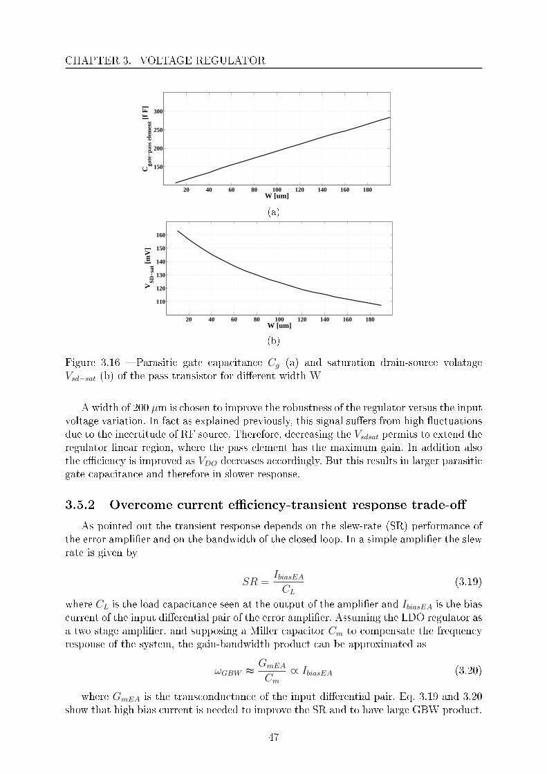
CHAPTER 3. VOLTAGE REGULATOR
20 40 60 80 100 120 140 160 180
150
200
250
300
W [um]
Cga
te−
pass el
emen
t [f F
]
(a)
20 40 60 80 100 120 140 160 180
110
120
130
140
150
160
W [um]
VS
D−
sat [m
V]
(b)
Figure 3.16 Parasitic gate capacitance Cg (a) and saturation drain-source volatageVsd−sat (b) of the pass transistor for dierent width W
A width of 200 µm is chosen to improve the robustness of the regulator versus the inputvoltage variation. In fact as explained previously, this signal suers from high uctuationsdue to the incertitude of RF source. Therefore, decreasing the Vsdsat permits to extend theregulator linear region, where the pass element has the maximum gain. In addition alsothe eciency is improved as VDO decreases accordingly. But this results in larger parasiticgate capacitance and therefore in slower response.
3.5.2 Overcome current eciency-transient response trade-o
As pointed out the transient response depends on the slew-rate (SR) performance ofthe error amplier and on the bandwidth of the closed loop. In a simple amplier the slewrate is given by
SR =IbiasEACL
(3.19)
where CL is the load capacitance seen at the output of the amplier and IbiasEA is the biascurrent of the input dierential pair of the error amplier. Assuming the LDO regulator asa two stage amplier, and supposing a Miller capacitor Cm to compensate the frequencyresponse of the system, the gain-bandwidth product can be approximated as
ωGBW ≈GmEA
Cm∝ IbiasEA (3.20)
where GmEA is the transconductance of the input dierential pair. Eq. 3.19 and 3.20show that high bias current is needed to improve the SR and to have large GBW product.
47

CHAPTER 3. VOLTAGE REGULATOR
However, with a high and xed value of bias current the eciency is aected especiallyat light load condition. The problem can be circumnavigated if the regulator adapts itsclosed loop response with the variations of the load current. This translates in higherquiescent current when the LDO is a high load state and lower quiescent current whenthe output is at light load condition. In this way it is possible to reduce the impact of theregulator on the power budget. The two techniques implemented in this work to achievethis condition are: class AB Error Amplier and adaptively bias Error Amplier.
48
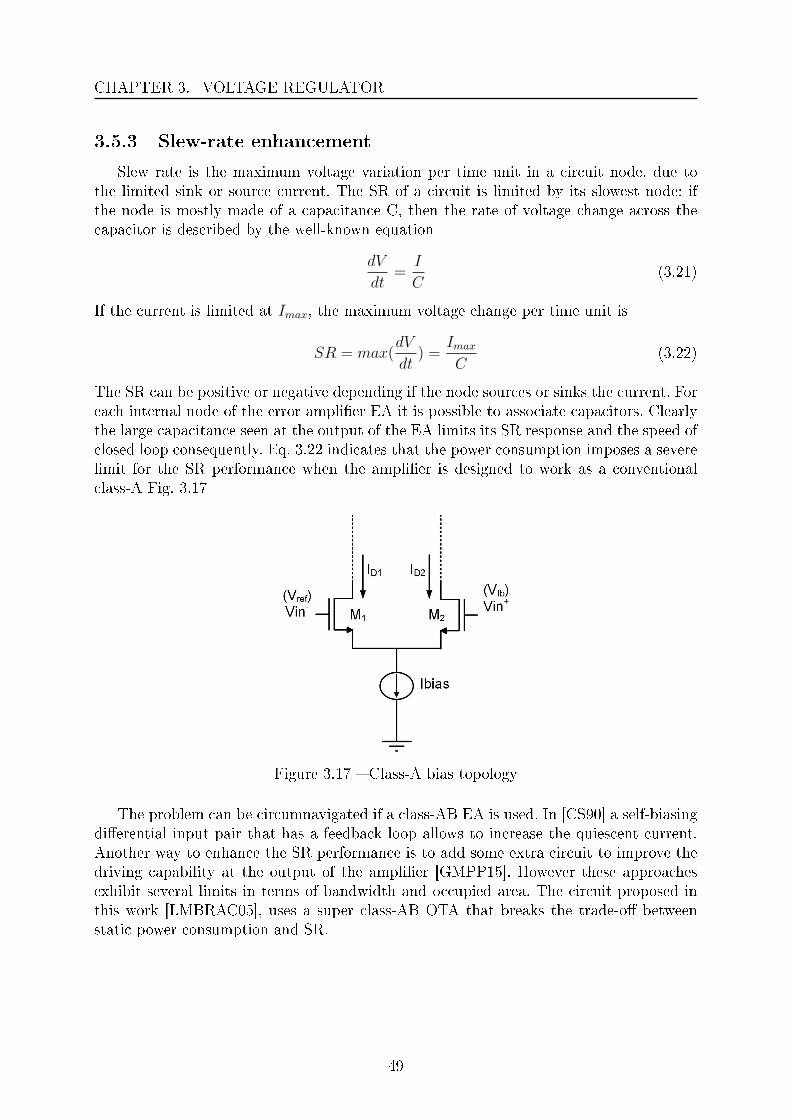
CHAPTER 3. VOLTAGE REGULATOR
3.5.3 Slew-rate enhancement
Slew rate is the maximum voltage variation per time unit in a circuit node, due tothe limited sink or source current. The SR of a circuit is limited by its slowest node: ifthe node is mostly made of a capacitance C, then the rate of voltage change across thecapacitor is described by the well-known equation
dV
dt=I
C(3.21)
If the current is limited at Imax, the maximum voltage change per time unit is
SR = max(dV
dt) =
ImaxC
(3.22)
The SR can be positive or negative depending if the node sources or sinks the current. Foreach internal node of the error amplier EA it is possible to associate capacitors. Clearlythe large capacitance seen at the output of the EA limits its SR response and the speed ofclosed loop consequently. Eq. 3.22 indicates that the power consumption imposes a severelimit for the SR performance when the amplier is designed to work as a conventionalclass-A Fig. 3.17
Figure 3.17 Class-A bias topology
The problem can be circumnavigated if a class-AB EA is used. In [CS90] a self-biasingdierential input pair that has a feedback loop allows to increase the quiescent current.Another way to enhance the SR performance is to add some extra circuit to improve thedriving capability at the output of the amplier [GMPP15]. However these approachesexhibit several limits in terms of bandwidth and occupied area. The circuit proposed inthis work [LMBRAC05], uses a super class-AB OTA that breaks the trade-o betweenstatic power consumption and SR.
49
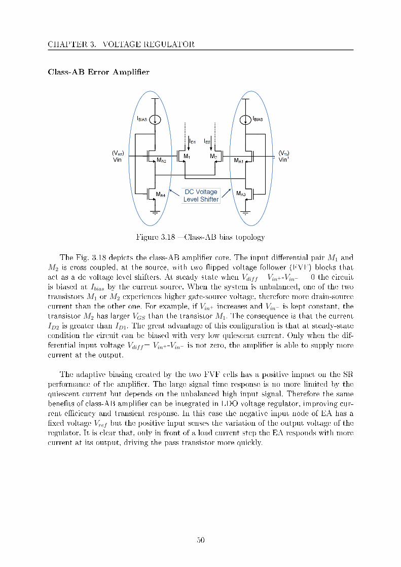
CHAPTER 3. VOLTAGE REGULATOR
Class-AB Error Amplier
Figure 3.18 Class-AB bias topology
The Fig. 3.18 depicts the class-AB amplier core. The input dierential pair M1 andM2 is cross coupled, at the source, with two ipped voltage follower (FVF) blocks thatact as a dc voltage level shifters. At steady state when Vdiff= Vin+-Vin− = 0 the circuitis biased at Ibias by the current source. When the system is unbalanced, one of the twotransistors M1 or M2 experiences higher gate-source voltage, therefore more drain-sourcecurrent than the other one. For example, if Vin+ increases and Vin− is kept constant, thetransistor M2 has larger VGS than the transistor M1. The consequence is that the currentID2 is greater than ID1. The great advantage of this conguration is that at steady-statecondition the circuit can be biased with very low quiescent current. Only when the dif-ferential input voltage Vdiff= Vin+-Vin− is not zero, the amplier is able to supply morecurrent at the output.
The adaptive biasing created by the two FVF cells has a positive impact on the SRperformance of the amplier. The large signal time response is no more limited by thequiescent current but depends on the unbalanced high input signal. Therefore the samebenets of class-AB amplier can be integrated in LDO voltage regulator, improving cur-rent eciency and transient response. In this case the negative input node of EA has axed voltage Vref but the positive input senses the variation of the output voltage of theregulator. It is clear that, only in front of a load current step the EA responds with morecurrent at its output, driving the pass transistor more quickly.
50

CHAPTER 3. VOLTAGE REGULATOR
Figure 3.19 Class AB error amplier
A Current Mirror OTA depicted in Fig. 3.19 is used to implement the Error Amplier.The pairs of transistors M5-M3, M4-M6 and M7-M8 act as current mirrors. Depending onthe ratio (K) between the aspect ratio (S) of the transistors, this topology can presentshigh transconductance, large BW and high SR, however at cost of higher output noiseand higher power consumption.
To get a rst estimation of the total quiescent current of the EA, and its impact on theregulator performances, a minimum current eciency of 60% was estimated for the outputcurrent of 1µA. Considering the quiescent current of 200 nA in the feedback resistors Fig.3.13, this leads to a global allowed quiescent current for the error amplier of around 200nA. The amplier is designed with the nominal unregulated input voltage of 1.2 V andeach transistor Mb is designed to supply Ib=30 nA. In order to bias the transistor M1 -M2 and MA1 - MA2 with the same current, it is needed to set S1/SA1 = S2/SA2 equal to1. Therefore the total current consumption of the circuit is given by:
Iqtotal = Ib(4 + 2K) (3.23)
To achieve the total current consumption of 180 nA, K is set to 1. In this low biascondition, all transistors operate in sub-threshold region and currents 4 drawing by M1
and M2 are given by
ID1 = IDO
(W
L
)M1
exp
[log
(IDA1
IDO(WL
)MA1
)− Vdiff
1
Vtn
](3.24a)
ID2 = IDO
(W
L
)M2
exp
[log
(IDA2
IDO(WL
)MA2
)+ Vdiff
1
Vtn
](3.24b)
where IDO is the technology current and it depends on the oxide capacitance, the substratefactor n and the carriers mobility µ0 and VT is the thermal voltage about 25 mV at roomtemperature.
4. Drain current equations of transistors M1 and M2 is obtained in Appendix
51

CHAPTER 3. VOLTAGE REGULATOR
Figure 3.20 FVF cell with cascode Pmos transistor
The above equations state that the drain current increases exponentially with the largeinput dierential voltage. However to avoid large current process-voltage-temperature(PVT) variations due to the exponential characteristic in weak inversion, the aspect ratioof Mb and the voltage Vb are set in order to keep the transistor in strong inversion. Itis worth noting that except Mb, all other transistors have to be oversized, because theyexperience more drain current than the 30 nA of current bias not only when the system isunbalanced, but also because the circuit provides extra bias current for the error amplierproportional to the variations of the load current. Consequently transistors M3-M4 aremuch larger than Mb. Therefore the transistors MA1-MA2 have lower Vds than M1-M2. Asa result the drain current is not the same. In order to re-equalize the circuit a PMOScascoding transistor Mcas is inserted in the feedback loop of each FVF cell (Fig. 3.20).They provide a level shift proportional to the bias voltage Vcas. Therefore the maximumvoltage at the drain of MA1-MA2 during idle mode is approximatively Vcas+Vsgcas. With acorrect setting of Vcas it is possible to re-balance the steady state drain current, howeverat the cost of extra power consumption.
The g (3.21a) depicts the voltage gain of the class-AB and class-A for a Ib= 60nA.The simulation highlights that the DC gain and the unity-gain frequency in the case ofclass-AB are doubled compared to the class-A. The graph shows 46dB versus 40dB and2.9 MHz versus 1.5 MHz. These results are explained by the fact that the dierentialac input signal is applied to both the gate and the source of M1 and M2. Therefore theinput signal sees a value of the transconductance double respect to the classical class-Atopology. In the Fig. 3.21b the great advantage in term of Slew-Rate is more visible, dueto the higher current delivered to the output thanks to the adaptively bias.
52

CHAPTER 3. VOLTAGE REGULATOR
(a)
(b)
Figure 3.21 Gain Voltage (a) and SR (b) simulation for Ib= 60 nA for Class-AB erroramplier in solid line and class-A dot line. The simulations are performed with CL=350fF.
53

CHAPTER 3. VOLTAGE REGULATOR
3.5.4 Extended closed loop Bandwidth
Figure 3.22 Adaptive biasing system. The rest of the circuit is omitted for simplicationpurposes
The second design step concerns the implementation of the circuit to adapt the biascurrent of the error amplier with the regulator load current. As explained previously,high bandwidth can be achieved with high quiescent current as indicated in Eq. 3.20.It is clear that the system is over-sized in terms of bias current when the output is atlight condition. Since high transconductance is needed only for high value of the outputcurrent, adapting the gm of the EA with the load current allows to reduce or to extend thebandwidth of the LDR regulator for the entire load range. Therefore a scaled version of theload current can be used for the Ibias of the Error Amplier, through 3 current mirrorsdepicted in g. 3.22. The rst reduction is acted by the pair of transistors Mp/MAB1,then the small replica of the load current is mirrored through the pairs MAB2/MAB3 andMAB4/MAB. Therefore the bias current supplied by the transistor MAB is given by
IAB =ILmn
(3.25)
where m is the scaled factor of the transistor MAB1 to the pass transistor Mp and n isthe aspect ratio between MAB4 and MAB. Considering that the transistors work in weakinversion for all load current range, the GBW product is proportional to
ωGBW ∝ Ibias + IAB (3.26)
However the design of the adaptively biased LDO (AB-LDO) requires a careful study ofthe loop stability, therefore the two aspects have to be evaluated at the same time.
54

CHAPTER 3. VOLTAGE REGULATOR
3.5.5 Compensation Strategy
As introduced in the section 3.4.1, to ensure the correct regulation the frequencyresponse of the closed loop LDO has to respect the stability criteria. In literature arereported dierent techniques to accomplish this task. Q-reduction technique in [LML07]is used to control the Q of the non dominant pole to compensate the regulator at lightload. For a multistage LDO regulator [GRF10] proposes a nested Miller Compensationwith a current buer, to move left-half plane zero towards high frequency. However themain drawbacks of these topologies is that they require big compensation capacitor andthe stability is ensured for a well dened minimum load current value.
The Miller compensation strategy with current buer [GPS12] is used in this workto ensure the stability for the entire load range. Miller capacitor is one of the techniqueswidely used to assure stable frequency response in a two stages amplier. However, thewell-known disadvantage of the LHP zero limits its strength, especially when a largecapacitor is needed to achieve pole splitting eect. The purpose of current buer is toalleviate the inuence of the left-right plane (LHP) zero breaking the forward path createdby the Miller capacitor. The frequency response of the voltage regulator can be associatedwith that of a two stages amplier. Therefore the same technique can be implementedto compensate the circuit. However the stability is more complicated to achieve due tothe load current large span. Respect to other approaches (nulling resistor, Voltage buer,poe-zero cancellation), the current buer allows to reduce the compensation capacitorvalue and not degrade the time response of the circuit [GPP08].
Figure 3.23 Block Diagram of two stages amplier with current buer compensationtechnique
55

CHAPTER 3. VOLTAGE REGULATOR
Figure 3.24 Transistor level design of the LDO voltage regulator proposed in this work
56

CHAPTER 3. VOLTAGE REGULATOR
Figure 3.25 AB loop gain for dierent load current
The Fig. 3.24 depicts the complete transistor level schematic of the LDO voltage regu-lator. It is possible to identify the pass transistorMp, the error amplier composed byM1
up to M8 transistors, the two class AB bias cells composed by MA1 up to MA4 with thexed bias transistor Mb and the adaptively bias transistor MAB and the adaptive biasingcircuit formed by transistors MAB1 up to MAB4. The compensation circuit is formed bythe current buer MR1-MR2/MC1-MC2 and the compensation capacitors CM and CMB.The feedback resistance Rfb1-Rfb2 are realized with a PMOS transistor to reduce the oc-cupied area. The circuit is designed to supply 1 V with a maximum output current of1mA. The unregulated input voltage range is (1.2-1.4)V. The voltage reference generatedby an ultra low power sub-bandgap is 650 mV. The values of feedback resistors are 2.6 MΩfor Rfb2 and 1.4 MΩ for Rfb1, which draw a ground current of 150 nA. One of the designtrouble is that the large aspect ratio of the pass transistor imposes a minimum draincurrent to properly work. For example, if the load current is about 100 nA the transistoris in o-state and the regulation is lost. Therefore to provide the correct operation for theentire current load range the minimum drain current for Mp is provided by the groundcurrent of the resistive network.
If we look closely to the circuit three loops can be identied. The most evident is themain loop needed to perform the regulation. The second is constituted by the AB networkto control the bias condition of the EA. The last loop is inside the main loop and is relatedto the Miller capacitor and the current buer. Therefore the LDO regulator has a stableresponse if the three loops respect the Phase Margin and Gain Margin criterion.The stability of the AB circuit can be assured if the loop gain is always less than 0 dB.Breaking the loop at the gate of the MAB (node at higher impedance), the loop gain isevaluated for the all load range current. The graphs in the Fig. 3.25 shows that the ABnetwork is always stable at every load condition, since that the loop gain is well above 0dB.
57

CHAPTER 3. VOLTAGE REGULATOR
Figure 3.26 LDO small-signal feedback representation
Once the stability of AB circuit is veried, the study of the frequency response can berelated merely to the LDO voltage regulator and the compensation circuit. As introducedin [GPS12] when a buer Miller compensation strategy is adopted the loop transfer func-tion presents one dominant pole and a pair of complex and conjugate poles. The presenceof the complex poles is due to the two nested loops. The open-loop transfer function isgiven by
T (s) = T (0)
(1− s
ZLHP
)(1− s
ZRHP
)(
1− spd
)(1 + s
GBWI+ s2
GBW 2IKIN
) (3.27)
where GBWI is the gain-bandwidth product of the internal loop and KIN is theseparation factor of the internal loop. The DC gain T(0) is equal to
T (0) = GmEARo−EAgmpRout (3.28a)
Rout = ro−pass||(Rfb1 +Rfb2) (3.28b)
the two zeros are
ZLHP =−GMc2
CMB
(3.29a)
ZRHP =gmp
CM + Cgd−mp(3.29b)
where GMc2 is the transconductance of the current buer, while the dominant pole isequal to
pd = − 1
[gmpRo−EA(CMB + CFB + CL)]Rout
(3.30)
58

CHAPTER 3. VOLTAGE REGULATOR
It is worth noting that the stability of the internal loop can be evaluated with theseparation factor K
K ≈ tan(φ) ≈ |p2|GBW
(3.31)
Where φ is the phase Margin and p2 is the rst non-dominant pole of the generic transferfunction. The separation factor KIN for the proposed voltage regulator is expressed by
KIN =|p2IN |GBWI
=
[CL(CFB + Cgp)Ro−EA + CMB
GMc2(CfbgmpRo−EA + CL)
]2
[gmpRo−EA(CMB + CFB) + CL]CLCMB(CFB + Cgp)Ro−EA
GMc2
(3.32)
where p2IN is the rst non-dominant pole of the internal loop and CFB = CM + Cgdp.With KIN=2 the PM = 65 and the system is stable with a small damping factor. Theminimum acceptable PM of 50 is forKIN=1.2. The same stability criteria can be adoptedfor the external loop. The separation factor KEX in this case is related also to the gain-bandwidth product of the external loop
KEX =GBWIN
GBWEX
(3.33a)
KEX =[gmp(CFB + CMB)Ro−EA + CL)]2[
CL(Cfb + Cgp)Ro−EA + CCM
GCA(CFBgmpRo−EA + CL)
]GmEARo−EAgmp
(3.33b)
Where GBWEX is the gain-bandwidth product of the external loop. With a valuegreater than 1.5 for both separation factors the overall stability is achieved. Following thedesign methodology given in [GPS12] the design equations for the compensation circuitare
CM =2Cgpn− 1
− Cgd (3.34)
CMB =4−KIN
BKIT
2Cgpn− 1
(3.35)
GMc2 =
4−KIN
BKIN
16KEXK
2I
1Gm−EA
− n2−14
CL
Cgp
1gminmp
(3.36)
n <
√64
KEXK2IN
CgpCL
gminmp
Gm−EA+ 1 (3.37)
Where B = K1K from Fig 3.24 and n is a scaling factor. Once the system is compensatedthe dominant pole and the second pole are expressed as
pD = − 1
gmpro−pass(BCMB + CFB)Ro−EA(3.38a)
p2 = − Gmp(BCCM + CFB)
CL(CFB + Cgp) + CMBCFBgmp
GCA
(3.38b)
59

CHAPTER 3. VOLTAGE REGULATOR
Some considerations have to be carried out about the two separation factors when anadaptively biasing topology is used. At rst glance, it is clear that KIN and KEX are notconstant for the entire load range. In fact both terms depend on the transconductance ofthe pass transistor gmp and on the output resistance of the error amplier Ro−EA. More-over the impact of the transconductance of the EA Gm−EA on the stability requires afurther study. From (Eq. 3.38a-3.38b) it seems that it does not have any inuence on thefrequency response of the regulator. However KEX is linked to Gm−EA and this is includedin the design equations (Eq. 3.36-3.37) for the compensation circuit. Given that Gm−EAchanges with the load current, it is important to understand which value has to be chosenin order to calculate n and GMc2. Observing the equation of KEX , the minimum valueoccurs when the transconductance of the error amplier is at highest value. Therefore,assuming a Weak Inversion region for the entire load current range, the minimum of KEX
is at heavy load condition. In conclusion Gmaxm−EA has to be used to design the compensa-
tion circuit.
So the study ofKIN andKEX can be related to gmp andRo−EA. Limiting the adaptivelybias current of EA, its output resistance does not change substantially. Therefore for therst approach, it is possible to consider that the stability depends largely on the passtransistor transconductance. To conrm this hypothesis, the (Fig. 3.27 3.28) show thetrends of KIN and KEX with the gmp and Ro−EA.
Figure 3.27 KEX for dierent values of Ro−EA and gmp. The minimum value of separationfactor is for light load condition. Ro−EA has negligible impact.
60

CHAPTER 3. VOLTAGE REGULATOR
Figure 3.28 KIN for dierent values of Ro−EA and gmp. The minimum value of separationfactor is for light load condition.Also in this case Ro−EA has negligible impact.
3.5.6 Transistor Level Design
Once the design equations are established and with the constraints dictated by theapplication, the design steps of the proposed LDO regulator can be as follow
achieve high current eciency (> 99%) from moderate to heavy load. Consideringthe 300 µA as the moderate load condition the total quiescent current of regulatorhas to be less than < 3µA. Being the EA the most power hungry block it is possibleto estimate the maximum bias current. With the aim of Eq. 3.23 the ImaxAB is
ImaxAB =Iq6− Ib (3.39)
Assuming 60% of the total quiescent current, thus extending the eciency belowthe moderate load, ImaxAB ≈ 200nA.
With Eq. 3.25 and with the above value, the scaling factors product mn is about5000.
Once all bias condition established, it is possible to calculate the compensationelements Eq. (3.34-3.37). Therefore, setting IminL = 300 nA and ImaxAB = 200nA,the related transconductances are gminmp = 8,78µS and Gmax
mEA = 6µS. The minimumload current is stated to stand-by mode. KIN and KEX are both set equal to1.8 to achieve a minimum phase margin of 60. The output capacitor is 20pF. Theparasitic gate capacitance of the pass transistor is about 200 fF. The buer currentgain is B = 1 in order to save the power consumption. The accepted trade-o is alarger occupied areas due to a higher value of the required compensation capacitors.The obtained values are CM = 2pF, CMB = 3.3 pF and GMc2 = 2.5 µS.
The Fig. 3.29 shows the increasing of IAB with the ILoad. The Fig. (3.30-3.31) show thebenets of AB circuit, where the current eciency is kept above 99% when the load currentis higher than 300 µA, while for low load current the system ensures a good value around70%. At the same time, the GBW of the loop moves from 40 kHz when the output isunder light condition, to around 360 kHz under heavy condition, improving the regulatortransient response.
61

CHAPTER 3. VOLTAGE REGULATOR
Figure 3.29 The trend of the bias current adaptability versus the load current.
Figure 3.30 LDO quiescent current and current eciency versus load current. In thiscase the trend is shown only for operation mode (ILoad= 1 µA-1 mA). For stand-by modethe current eciency is worsen by the minimum drain current needed to keep ON thepass transistor.
62

CHAPTER 3. VOLTAGE REGULATOR
(a)
(b)
Figure 3.31 (a) Open loop gain for ILoad = 1 µA (black line) and for ILoad = 1 mA (blueline). It is evident the GBW product is increased at heavy load condition due to higherGmEA. GBW extends from 40 kHz to 360 kHz (b) Phase for the two load conditions.
63

CHAPTER 3. VOLTAGE REGULATOR
Figure 3.32 Phase margin versus output capacitor value, for dierent stand-by outputcurrent values. From Istand−byL = 205 nA (dash line) to Ioperation−modeL = 1 µA (solid line).
Figure 3.33 Phase margin versus output capacitor value at heavy load condition
Generally, depending on the fabrication technology, the output capacitor can be inte-grated for values up to 100 pF. As previously explained, higher value allows to respondmore quickly to current demand in the case of low to high step, because it acts as chargesupply. However the frequency response and the stability are largely aected by the valueof this output capacitor. With the compensation topology adopted in this circuit thereis a trade-o between the minimum Phase Margin achievable under stand-by conditionand the value of output capacitor. Fig. 3.32 shows that the phase margin is inverselyproportional to the value of CL. For example for the designed circuit the stand-by outputcurrent is 250 nA (dashed line) and the output capacitor value is 20 pF, thenthe PMachieved is about 70. Therefore if CL is replaced by a larger capacitor of 50 pF to reducethe output voltage spike, the minimum stand-by current has to be increased, to about800 nA (dash-point line), to achieve the same PM of 70. Fig. 3.33 shows that heavy loadcondition the output capacitor has no impact on the phase margin. A minimum phasemargin of 90 (Fig. 3.34) is achieved in operating range assuring a stable regulation alsowith a light load.
64
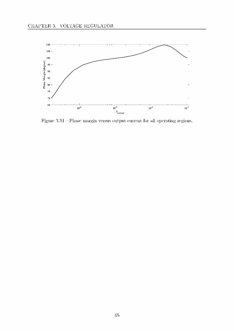
CHAPTER 3. VOLTAGE REGULATOR
Figure 3.34 Phase margin versus output current for all operating regions.
65

CHAPTER 3. VOLTAGE REGULATOR
Error Amplier The transistors sizes of the error amplier are chosen with the aid ofthe inversion coecient IC 5
IC =ID(WL
)I0
(3.40)
For the MOS technology used in this work, the technology current I0=0.63 µA for N-channel transistor and I0=0.187 µA for P-channel transistor. The other two design pa-rameters are the drain current and the channel length. Since the drain current is xed bythe application, the size is related to the choice of the IC and the channel length to cal-culate the width of transistor. All transistors work at low side of the moderate inversion.This is an accepted trade-o between transconductance-current eciency and frequencyresponse. Moreover in this region the transistor achieves high power eciency and lowvoltage bias. Therefore the range of IC considered for the design is between 0.1 and 0.5.Minimum channel length is avoided for all transistors in order to make the circuit morerobust against Vgs and Vth mismatch. Moreover longer channel transistor operating at lowside of Moderate Inversion exacerbates frequency response. Therefore a L = 0.7 µm forall transistors is chosen to limit the parasitic capacitance associated to the internal nodeof the circuit.
The bias transistor Mb as previously introduced is the only device that operatesin strong inversion. With a drain current of 30 nA this operation mode is possiblebecause the gate voltage is externally driven. The channel width is 0.35 µm.
The input signal transistors M1-M2 and MA1-MA2 are sized with an IC = 0.3,to limit drain current mismatch due to threshold voltage variations. Assuming anhigher drain current dictated by the class-AB operation (≈ 500nA) the resultingW is equal to 1.8 µm. The nal value is decreased to 1.4 µm to accomplish layouttechniques as common centroid or interdigitized topologies.
The two sink transistors MA3-MA4 have to support twice the drain current thanthe input signal transistor. This leads to W = 2.8 µm.
For the PMOS current mirror transistors M3 to M6 the main trade-o is betweenthe drain current mismatch and the DC gain of the Error Amplier. Therefore,with IC = 0.5 the W equals 3.5 µm.
The same design criteria is adopted for NMOS sink current mirror M7-M8. Thisleads to W = 1.4 µm.
The PMOS cascode transistor is designed to have a Vsg = 200mV. With a draincurrent of only 2 nA, the transistor has to operate in deepWeak inversion. Thereforefor IC = 0.01 W equals 0.7 µm
Adaptively Bias Circuit The adaptively bias circuit is designed to transfer a scaledversion of load current with a scaled factor of 5000. Moreover it is designed to be com-pletely o at light load condition. In order to draw a low quiescent current the factor n ≈10000. Therefore the total quiescent current for the circuit at heavy load is about 140 nA,where each branch draws 70 nA. The aspect ratio of the transistors are: SMAB1
= (0.44
),SMAB2−MAB3
= (0.77
) and SMAB4= (2.8
0.7). Finally to achieve the desired scaling factor m =
1/2, the aspect ratio of SMABequals (5.6
0.7).
5. Introduced in chapter one.
66

CHAPTER 3. VOLTAGE REGULATOR
Current Buer The current buer is designed to present a transconductance of 2.5 µSto compensate the feedback loop. At weak inversion the equivalent current is about 80nA. With a L = 0.7 µm and a IC = 0.1, the width of channel is W = 1.4 µm. The currentmirror is designed to have B = 1, so the two transistors have the same aspect ratio ofSMC1−MC2 = (1.4
0.7).
3.6 Voltage Reference
Most of the time, nominal operation conditions of electronics devices can change due toextreme variation of environment property or to external interference. Especially temper-ature is one of the main factor, since that many of transistor parameters are temperature-dependent. The main goal of voltage reference is to generate a stable voltage independentto supply voltage and temperature. An independent supply voltage circuit means thatonce the equilibrium point is reached the bias condition does not change with the supplyvoltage. However to eliminate the thermal dependence, it is needed to create two quanti-ties (voltage or current) exhibiting an opposite trend with the temperature.The three main aspects to be evaluated to quantify the robustness of a voltage referenceare: temperature coecient, power supply rejection ratio PSRR and the minimum supplyvoltage.
Temperature Coecient
The temperature coecient quanties the output voltage variations respect to thetemperature.
TCeff =1
Vref−nom
(Vref−max − Vref−min
Tmax − Tmin
)(3.41)
where Vref−nom, Vref−max and Vref−min are the output reference voltages at room nominalmaximum and minimum temperatures.
PSRR
It is a small-signal characteristic and indicates the capability of voltage reference tosuppress the voltage ripple coming from the voltage supply
PSRR = 20log
(δVrefδVDD
)(3.42)
where δVref is the ripple of the output voltage.
Minimum Supply Voltage
The minimum supply voltage is the value from which the output voltage reference isconstant. Normally it is measured at room temperature.
67

CHAPTER 3. VOLTAGE REGULATOR
Figure 3.35 Ueno voltage reference
State of the Art
Ueno Voltage Reference The circuit proposed in [UHAA09] (Fig. 3.35) generates thevoltage reference with all transistors in Weak Inversion (WI), excepted the transistor M8
that acts as resistor being in triode region under Strong Inversion condition. As explainedthe voltage reference has to be supply independent; in this case the transistors M1-M2
and M8 with the two relative mirror current PMOS transistors generate the current ina self-bias way. This current is then mirrored in the other three branches. The outputvoltage reference is then equal to
Vref = Vds7 + Vds6 + Vds4 = Vgs7 + Vgs6 − V gs5 + Vgs4 − V gs3 (3.43)
As the transistors work in WI, the Eq. 3.43 can be rearranged as
Vref = Vgs4 + nVtln
(S5S3
S6S7
)(3.44)
Eq. 3.44 shows that a Vref independent from the temperature can be obtained if the twotemperature coecients of the two terms on right side of the equation are opposite. Thiscircuit oers the advantage of eliminating resistors that for nanopower circuits assumehigh values and therefore large silicon area.
De Vita Voltage Reference To accomplish the main task of voltage reference, in[VI07] the temperature dependence of electrons mobility is eliminated.
The transistors M1 and M7 (Fig. 3.36) have gate oxide thicker than the others sohigher threshold voltage. In this way the transistors M1-M7 and M2-M8 are biased in WIand SI respectively. The current I0 generated in the load M9 is proportional to the squareof thermal voltage and the carrier mobility
I0 =µCoxS8
2(√
S8
S2− 1)2η
2Vt2ln2
(S7
S1
)(3.45)
68

CHAPTER 3. VOLTAGE REGULATOR
Figure 3.36 De Vita voltage reference
Since the load transistor is a diode connected in saturation region under SI conditions,the output voltage reference is given by
Vref = Vth10 +ηVt(√S8
S2− 1)√S8
S9
ln
(S7
S1
)(3.46)
Adjusting the aspect ratio of transistor involved in the Eq. 3.46 the temperature depen-dence of the output voltage reference can be eliminated.
Bandgap Voltage Reference Normally the use of bipolar transistor as current refer-ence in the circuit makes the output voltage equal to the bandgap voltage of the silicon(≈ 1.12 V).
Figure 3.37 Bandgap Voltage reference proposed in [HUKN10]
The output voltage reference generated by the circuit is given by
Vref = VBG +
(ψVbe,T +
5∑i=0
Vtln
(S2i
S2i−1
))(3.47)
69

CHAPTER 3. VOLTAGE REGULATOR
where Vbe is the silicon bandgap voltage, ψVbe,T is the temperature coecient of base-emitter voltage. Choosing a correct aspect ratio of the involved transistors, the secondterm in the right side of the equation can be reduced to zero.
In conclusion all the introduced circuits share dierent aspects: To eliminate the temperature dependence 2 quantities are needed: one that has a
negative temperature coecient CTAT (complementary to absolute temperature),that can be generated by a voltage or a current. The other has to increase withthe temperature (proportional to absolute temperature PTAT) and the weight ofboth has to be equal.
All circuit are working with a quiescent current in the range of nano-ampere. Togenerate this low current, large resistors are required with a prohibitive occupiedarea. Therefore only transistor must be used.
The main problem in the design of a voltage reference is the process variations. Theexponential trend of drain current in WI region strongly impacts the performancesof the circuit, since the deviation from nominal value is more important than inSI. Moreover the change in the threshold voltage due to the process variation canaect the stability of the output voltage reference. These considerations have to betaken in account into the design ow.
70

CHAPTER 3. VOLTAGE REGULATOR
3.7 Circuit Design
Figure 3.38 Sub-bandgap voltage reference used in this work
The voltage reference implemented in this work is based on [MKB14]. In the left sideof the Fig. 3.38 the CTAT voltage generator is made with the bipolar transistor Q and theMOS transistorsM1-M2.In fact the voltage at the node X, simply the base-emitter voltageof Q, is equal to Vgs1+Vgs2. Therefore the gate-source voltage of M1 can be expressed as
Vgs1 =Veb2
(3.48)
This relation is true if the two MOS transistors have the same width and length channeland if the bulk-source voltage is equal to zero. As the CMOS technology process addressedin the present work allows a triple n-well conguration it is possible to tie the bulk nodeto the source potential. The pair of transistors M9-M2 acts as the rst PTAT voltagegenerator. With this conguration Vds2 = Vgs2-Vgs9 and it can be expressed as:
Vds2 = nVtln
(pS9
S2
)(3.49)
where p is the number of times that the reference current Iref is replicated to generatethe PTAT voltage. To create a self-biased circuit, the voltage at node X is generated bythe feedback path through the current mirror M11-M10. In this way choosing the factorK and the aspect ratio of transistors M1 a non zero equilibrium point can be achieved.With the Eq. 3.48 and knowing that IQ=Iref ×K, Veb can be expressed as
Veb = Vt2mn
2n−m
[ln
(ID0K
Isat4A
W1
L1
)+VthnVt
](3.50)
71

CHAPTER 3. VOLTAGE REGULATOR
where n is the slope factor of MOSFET transistor, m and A and Isat are the slope factor,the emitter surface and the saturation current of the bipolar transistor. At this pointto counterbalance the CTAT voltage, the only PTAT cell created by transistor M9-M2
is not enough. Thus, 3 cascaded source-coupled [VN78] cells are added to eliminate thetemperature dependence. To ensure the correct function of every cell, the top transistorhas to be in saturation region. Moreover the drain current has to be greater than theleakage current of MOSFET and lower than the value for which the transistor stops towork in WI. Every cell generates a PTAT voltage equal to the drain-source voltage ofbottom transistor
VPTAT = Vds,bottom = ηVtln
(Id,bottomStopId,topSbottom
)(3.51)
The maximum generated voltage is around 100 - 120 mV. Therefore the total PTATvoltage is given by:
VPTAT,tot = ηVtln
[I7I5I3I2
I8I6I4I9
W8
L8
W7
L7
W6
L6
W5
L5
W4
L4
W3
L3
W9
L9
W2
L2
](3.52)
Finally the output voltage reference is expressed as
Vref = Vgs1 + VPTAT,tot (3.53)
Setting the aspect ratio of transistors and the current multiplication factor given by thenumber of stages in cascade, it is possible to obtain the CTAT coecient temperaturewhich cancels the thermal dependence of output voltage. Surely one of the main designcriteria is the power consumption. But as explained previously the drain current has to behigher than the leakage current. Moreover the aspect ratio of transistors is an importantparameter to be taken in account, since it impacts the PTAT coecient and has to simplifylayout techniques as in the case of common centroid. Considering this limitation, it waschosen S1 = S2 = 4 and K = 4. The currents Iref = I1 = I2 = I3 = 6.5 nA, thus thecollector current of Q is equal to 26 nA. This leads to have Vx = 0.584 V. The aspectratio S9 is 18. The remaining transistors exhibit a form factor S4,6,8/S3,5,7 = 5. Thereforethe nominal output voltage reference obtained at 27 C is 650.4 mV. The total quiescentcurrent is 52 nA, for a power consumption of 62.4 nW.
Table 3.3 Transistors Size
Transistor Aspect Ratio
M11 M12 M13 M14 (2/1)
M10 (8/1)
M9 (18/1)
M2 M1 (4/1)
M4 M6 M8 (10/1)
M3 M5 M7 (2/1)
Q 1 (emitter area)
72

CHAPTER 3. VOLTAGE REGULATOR
Sub-bandgap simulation results
Figure 3.39 Output voltage reference versus the temperature
(a) (b)
Figure 3.40 The quiescent current (a) and the voltage reference (b) versus supply voltage
Fig. 3.39 shows the dependence of Vref on the temperature range. The curve exhibitsthe typical curvature due to the non-linearity of BJT base-emitter voltage. The temper-ature coecient is about 15.9 ppm/C. The line regulation is 4.75 mV/V from 1V to 2Vof supply voltage Fig. 3.40(b). From Fig 3.40(a) it is evident that once the CTAT volt-age circuit reaches the equilibrium point, for VDD = 0.95 V, the current remains almostconstant for the entire supply range. MonteCarlo simulations was performed (Fig. 3.41)to take into account process variations and mismatch. The results shows a mean of 650.4mV with a standard deviation of σ = 15 mV. The main disadvantages of WI, is that theprocess variations have a greater impact on the circuit performances.
73

CHAPTER 3. VOLTAGE REGULATOR
Figure 3.41 Monte Carlo simulations on the output voltage reference with 100 runs.
3.8 Voltage Regulator Simulation Results
Figure 3.42 Line regulation (orange line) of LDO when VIN moves from 0 V to 1.6 V.The simulation is performed at heavy load condition.
The nal design has been realized in 130 nm Standard CMOS process from ST Mi-croelectronics. Each simulations are performed with sub-bandgap circuit. The Fig 3.42shows the line regulation of the LDO up to input voltage of 1.6 V. The minimum Vin forwhich the output is at its nominal value of 1 V is about 1.095 V. The LDO shows a lineregulation about 17 mV/V. As expressed in the Eq. 3.4 high loop gain is preferable toreduce the variations at the output voltage.Load regulation is represented in Fig 3.43. The LDO shows a Load regulation about 6mV/mA. Also in this case high loop gain helps in reduction of output voltage variations.This is evident in the rst part of graph where the circuit is at lower bias point. In thisrange the slope is more accentuated than the second part, because the regulator presentslower open loop gain. Therefore the DC accuracy performances of LDO are dictated bythe trade-o accepted in the design stage.The transient responses of the regulator are depicted in (Fig. 3.44, 3.45 and 3.46) forthree dierent situations. All rise and fall current steps are equal to 100 ns. In Fig. 3.44
74

CHAPTER 3. VOLTAGE REGULATOR
Figure 3.43 Output Voltage versus output current
the load current changes from 1µA to 1 mA and indicates the operation mode of theregulator. The advantage of the adaptively bias is well evident in terms of speed response.In fact the transient time decreases from 3.2 µs without the adaptively bias to 0.78 nswhen the circuit is inserted. It is worth noting that the magnitude of voltage spike is thesame for both circuits. This is because at rst time the error amplier counteracts theoutput voltage variation slewing the gate capacitance of pass transistor. Only when thevoltage changes at the EA output, the adaptively bias circuit supplies more current to theamplier, therefore the bandwidth of closed loop extends accordingly. It is clear that thetwo circuits with the same EA at the same bias point present an identical voltage spike.The situation appears dierent when the output current moves from moderate conditionto heavy condition as in Fig. 3.46. In this case, at the starting point the closed loopbandwidth of the LDO is larger for the adaptively bias topology and the spike reductionis about 15 mV.The Fig. 3.47 shows the simulation result in the case of an input voltage step at heavy loadcondition. Besides the improvement in speed response, the adaptively bias gives betterresults in term of noise suppression. In fact the PSR at very low frequency is inverselyproportional to the closed loop gain. The Fig. 3.48 underlines that when the adaptivelybias circuit is removed the power supply rejection is at very low value of -10 dB, whilewith adaptively bias circuit the improvement is of about 25 dB. Montecarlo simulationswere performed for the phase margin (PM) (Fig. 3.49) and output voltage Fig. 3.50. Inparticular for the PM only worst cases were addressed. The results shows a mean of 92
with a standard deviation of σ = 0.67 for Iload = 1µA and a mean of 65 with a standarddeviation of σ = 3.9 for stand-by condition. For the output voltage the two extremes ofthe operating condition were addressed. In this case a mean of 1.029 V is obtained witha standard deviation of σ= 0.025 V for Iload = 1µA. For Iload = 1mA the regulator showsa mean of 1.004 V with a standard deviation of σ= 0.024 V.
75

CHAPTER 3. VOLTAGE REGULATOR
Figure 3.44 Transient response for a load current step in operation mode. From 1 µAto 1 mA.
76
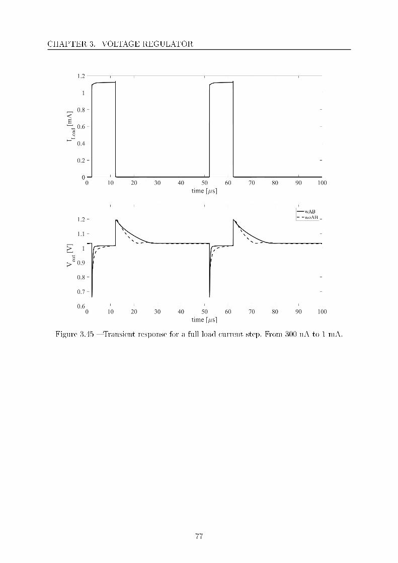
CHAPTER 3. VOLTAGE REGULATOR
Figure 3.45 Transient response for a full load current step. From 300 nA to 1 mA.
77

CHAPTER 3. VOLTAGE REGULATOR
Figure 3.46 Transient response for a load current step in moderate condition. From 300µA to 1 mA.
78

CHAPTER 3. VOLTAGE REGULATOR
Figure 3.47 Line transient at heavy load condition
Figure 3.48 PSR at heavy load condition
79

CHAPTER 3. VOLTAGE REGULATOR
Figure 3.49 Monte Carlo simulations on the phase margin with 100 runs.a) for stand-bycondition b) for minimum operating load condition
80

CHAPTER 3. VOLTAGE REGULATOR
Figure 3.50 Monte Carlo simulations on the regulator output voltage with 100 runs. a)for minimum operating load condition b) for maximum operating load condition
81

CHAPTER 3. VOLTAGE REGULATOR
3.9 Conclusion
An adaptively biased LDO regulator has been designed for harvesting applications.Class AB Error Amplier and adaptively bias circuit have been adopted to improve thetransient response with high current eciency under all load condition. The stability ofthe feedback loop has been guaranteed by the Miller compensation capacitor with theaid of the current buer. The regulator exhibits a minimum PM about 65 for a loadcurrent lower than the minimum value in operating range. In this way the stability hasbeen ensured also under stand-by condition.When the adaptively bias is inserted, the time to recover the nominal output voltage islesser than 1 µs consuming only 2,25 µW under heavy load condition. Also AC perfor-mances take advantage because the error amplier exploits higher voltage gain due tohigh quiescent current. The FOM = tr
IqIload,max
is introduced to compare the dierent de-
signs, lower value means better performances. Larger FOM respect to [KM14], where thequiescent current is constant for all load range, is balanced by a better current eciencyespecially at light load condition. However, considering the strict requirements for theregulator, the designed LDO is well suited for harvesting applications.
Table 3.4 Comparative switching regulator
[KM14] [ZG12] This Work
Vout (V) 1 - 1
VDO (V) - 0.109 0.12
CL (pF) - 2 20
Iload,max(mA) 5 5 1
Iq(µA) 99.04 12 1.8
Eciency 98 99 99.9
tr (µs) 0.161 2 0.9
FOM (ns) 3,18 4,8 1,62
82
Chapter 4
Ultra-Low power transmitter
Transmitter is one of the most hungry circuit in a communication system. Especiallyin long range transmission, where high output power level (> 20 dBm ) is required, thepower amplier (PA) needs high quiescent current to assure high voltage gain. Moreoverthe system requires a stable frequency carrier and a clean spectrum to avoid adjacentchannel interference. Clearly satisfying all those requirements means complex system andthus higher power consumption. To comply the necessity imposed by the energy constrainsin harvesting system, the design approach of transmitter has to be revisited. At rst thecommunication distance is no more longer than 10 m and thus the transmission powerlevel is in the range of tens-hundreds of µW (-20 dBm to 0 dBm). Therefore when thecommunication distances decrease, as in the case of the WSN, the PA weight in termsof power consumption is comparable with that of the local oscillator LO and matchingnetwork MN.For example adopting high performances receiver, with a frequency correction loop scheme,is possible to use simple and not very accurate local oscillator on the transmitter side.In this way it is possible to avoid high power PLL based frequency generator or highcost crystal reference based system. As reviewed in chapter 2, a non coherent modulationscheme (OOK or FSK) permits to reduce the power consumption and relax the poweramplier linearity, and the low-complexity architecture is a favorable point for ULP trans-mitter. Unfortunately this conguration suers from a poor spectral eciency.In summary the paradigm "less is better" can represent a way to demolish the problemat-ics of power consumption in ULP transmitter design. Clearly the performances achievablecan not be comparable to the classical transmitter and depending on the application someaspects have to be sacriced.
83

CHAPTER 4. ULTRA-LOW POWER TRANSMITTER
4.1 Transmitter architecture
Figure 4.1 Block diagram of two-step conversion transmitter
A classical two-step transmitter is depicted in Fig. 4.1. This topology is a modi-ed version of direct-conversion architecture in order to avoid injection pulling phenom-ena [Raz99]. In fact one of the main problems is the high power signal at PA output,which can modify the frequency oscillation of the LO. With the two-step transmitter thePA spectrum is quite far from the frequency generated by the VCO, reducing the risk offrequency shift. However the number of blocks required to achieve high spectrum eciencyand clean frequency are not negligible, unlikely this high power solution can represent agood approach for the target of this work.Since that in short distance communication the PA output power level is not high, thefrequency pulling is less probable and a direct modulation scheme can be a optimum so-lution to implement very low-power transmitter. In fact only three blocks are needed togenerate the RF signal, where the modulation is normally done in the frequency gener-ation circuit Fig. 4.2. Both on-o keying (OOK) and frequency shift keying (FSK) canbe implemented where the baseband signal directing modulates the signal transmission.Moreover non-linear high ecient power amplier can be adopted.
Figure 4.2 Block diagram of direct modulation transmitter.
It is clear that in direct modulation architecture every block has a more importantimpact on overall eciency respect to the high output power transmitter where the maindesign eorts are addressed to improve the PA ecient. Therefore the global transmittereciency can be written as
ηTX =Prad
PDC,PA + PDC,LO + PDC,mod=
ηPA
1 + ηPAPDC,LO
Prad+ ηPA
PDC,mod
Prad
(4.1)
84
CHAPTER 4. ULTRA-LOW POWER TRANSMITTER
where Prad is the radiated power level, PDC,LO PDC,PA and PDC,mod are the DC powersdissipated by the local oscillator, the power amplier and the circuits which generate themodulation signal. It is worth noting that the maximum attainable PA eciency ηPA notonly depends on the PA operating class, but in short distance communication the matchingnetwork eciency has a crucial role in terms of power transmission capability. From theanalysis in [HP06] the eciency of a generic L-matching network can be expressed as
ηMN = 1− Q
QL
− Q
QC
≈ 1−
√Ropti
Rs− 1
QL
(4.2)
where QL and QC are the quality factor of inductor and capacitor, Q is the total qualityfactor of matching network that depends on the transformation ratio between the optimumresistance Ropti and the antenna resistance Rs. The approximation is valid only up to10 GHz, where the poor inductor quality factor dominates the overall eciency. Someconsiderations will be done further about the problematics of matching network designwhen the radiated power is in the range of tens of µW. Even if the transmission eciency(Eq. 4.1) gives us an instantaneous photography of the transmitter capability to save theavailable power, this does not highlight the energy cost to transmit a certain amount ofdata. Moreover, in WSN the transmitter is in stand-by mode for the most part of time.An useful metrics used to evaluate the transmitter is the energy per bit (Ebit) needed totransmit a packet of information
Ebit,DC = Ebit +PDC,stand−byDC ×DR
(4.3a)
Ebit =PDC,totDR
(4.3b)
Where DR is the data-rate and PDC,tot and PDC,stand−by are the total powers burned bythe transmitter in active and stand-by mode respectively, DC is the duty cycle. Howeverthis metric does not facilitate the comparison between dierent topologies. As rst itdoes not provide information about the radiated power, second to recover the informationabout the power dissipated in stand-by mode is not always possible. Therefore generallyonly Ebit is used to compare dierent transmitters. To have a more complete framework,the FOM introduced in [TLHL14] [VHH+11c] can be used to evaluate the performancesof dierent topologies
FOM =EbitPrad
(4.4)
The above equation relates the transmission eciency and the data rate highlighting therelation between the transmitter architecture and the application/standard.
85

CHAPTER 4. ULTRA-LOW POWER TRANSMITTER
State of the Art
Figure 4.3 FOM versus data-rate for recent ULP transmitter. [KPL17]
In Fig. 4.3 representative ULP transmitters are classied based on the normalizedFOM for respective data-rate. As can be seen most of them adopt a data-rate between1 and 10 Mbps, proving that in general the information processed in WSN does notrequire high amount of data. For example the transmitter (dot 9 in the g.4.3) proposedin [KCSN14] is designed to have high bandwidth to support high data-rate, where thecapsule endoscopy system uses high amount of data to generate high resolution imagefor accurate diagnosis. At the opposite side, for transmitter (dot 1 in the g.4.3) lowerdata-rate is chosen for peer-to-peer communication. The architecture is based on multi-phase injection locking [PO11] where the frequency of injected signal is generated at 45MHz through a stable crystal reference. Then the dierent phase-shifted signals from theinjection locking ring oscillator ILRO are merged in a PA/EDGE-combiner EC Fig 4.4.
Figure 4.4 Block diagram of sub-harmonic injection locking transmitter [PO11].
The same sub-harmonic injection-locking architecture is used for transmitters (dots 3and 10 in the g.4.3), at the same carrier frequency of 400 MHz. The dierence in thiscase is the amplication stage that is provided by a class-C power amplier. The maindrawbacks of this architecture are the o-chip matching networks where the frequency
86

CHAPTER 4. ULTRA-LOW POWER TRANSMITTER
transmission of 400/500 MHz makes hard the passive integration. An extremely low com-plexity transmitter (dot 4 in the g.4.3) is presented in [MBL+13]. The transmitter iscomposed by a direct-RF power oscillator, where the inductor acts as resonator and ra-diating element. The carrier frequency in this case is 2.4 GHz. The cross-coupled NMOSoscillator is tail-biased with ultra-low leakage transistor to reduce the stand-by leakagepower. The transmitter is designed to support both FSK and OOK modulation.
Figure 4.5 Power VCO transmitter presented in [MBL+13].
From the above analysis, ULP transmitters for short distance range prefer non con-ventional architecture to reduce the power consumption with low output power andmedium/high data-rate. However good performances can be achieved with classical archi-tecture. In the next section several classical direct modulation architectures are reviewedsupported by a design guideline to achieve low power consumption.
87

CHAPTER 4. ULTRA-LOW POWER TRANSMITTER
4.2 ULP Direct Modulation Transmitters.
In classical direct modulation transmitter, optimizing not only PA but also LO andMN is possible to achieve low-power condition, especially with modern devices where thetransition frequency easily exceeds 100 GHz for submicron technology. For example, theSTMicroelectronics 130 nm CMOS technology oers MOS transistors with a peak fT of120 GHz. In addition, the MOSFETs used in low power applications are generally smalland therefore, their peak transition is higher than bigger transistors, even if the lowertransconductance due the low bias current soothes this improvement. In any case, thishigh peak fT allows subthreshold operation, in order to reach higher transconductanceeciency (gm/Id). As a consequence, the same RF performances are achieved at lowerpower consumption. Another design key point is the choice of voltage supply. As the powerconsumption is directly proportional to V 2
dd, decreasing the supply voltage considerablyenhances the circuit eciency. A lower Vdd also reduces the electric elds in the deviceand improves its long term reliability. On the other hand, low Vdd reduces the voltageheadroom available for cascading transistors, invoking folded solutions.In the next section the design considerations and the techniques as well as the dierentcircuit blocks of the transmitter are described.
4.2.1 Local Oscillator
The carrier frequency generation can be done through voltage control oscillator VCO.The VCO can be classied in two main architectures: ring oscillator and LC oscillator.Irrespective of the topology the equation for the instantaneous VCO frequency is
fV CO = fo +KV COVctrl (4.5)
where fo is the free-running frequency, KV CO is the gain of the VCO that settles howmuch a change in control voltage will change the VCO frequency. Vctrl is the voltage toset the frequency at the desired value.A ring oscillator is formed by a odd number of delay stages, where the output of the laststage is brought back to the input of the rst one. The oscillation is assured if the ringprovides a phase shift of 2π and has a unity voltage gain at the oscillation frequency. AVCO ring oscillator is depicted in Fig. 4.6
Figure 4.6 Current starved VCO
88

CHAPTER 4. ULTRA-LOW POWER TRANSMITTER
The frequency oscillation of a ring oscillator is
f =1
2Ntd(4.6)
where N is the number of delay cell and td is the delay time of each cells. As the oscilla-tion frequency is inversely proportional to the delay time and which depends on the biascurrent Iref , Vctrl provides control for the oscillation frequency.In LC oscillator the frequency is generated through a lossy resonator. In order to sustainthe oscillation a small-signal equivalent negative resistor has to be inserted to cancel outthe losses, generated by the inductor and capacitor parasitic resistor. Fig. 4.7 shows ageneral representation of an LC oscillator, pointing out the negative resistor.
Figure 4.7 LC resonator with negative resistor to compensate the losses due to parasiticresistor RP .
The frequency oscillation is given by the resonant frequency of LC tank (Eq. 4.7).To set the desired frequency, the circuit is designed with a tunable voltage capacitor(VariCap).
f =ωo2π
=1
2π√LC
(4.7)
One of the most important property of a VCO is its phase noise. In a noiseless VCOthe output voltage is expressed as
Vout(t) = A cos(ωot+ φ) (4.8)
where A is the output voltage amplitude and φ the phase. However in presence of a noisysource the amplitude and the phase are altered. In particular, as depicted in Fig. 4.8 ifthe noise is injected at the signal peak, the amplitude changes without phase shift, andit recovers its nominal value due to the limiting mechanisms in a real oscillator. Whileif the noise is injected during the transition Fig. 4.8, the signal phase is shifted and thisuctuation persists innitely [HLL99]. Therefore the Eq. 4.8 has to be rearranged asfollows
Vout(t) = A(t) cos(ωot+ φ(t)) (4.9)
where A(t) and φ(t) are the output voltage amplitude and phase time-dependent. Adenition of phase noise [MA08] is as follows
L(∆ω) = 10 log
( ∑NL,i
2∆ω2C2A2
)(4.10)
where NL,i is the white noise source and ∆ω the oset frequency from the carrier atwhich the phase noise is measured. One of the unwanted eect of phase noise is the down-conversion of adjacent channels in the band of the desired signal.
89

CHAPTER 4. ULTRA-LOW POWER TRANSMITTER
Figure 4.8 Output voltage variation in presence of noisy source. At the left side the noiseis injected at the peak voltage, at the right side the noise is injected at zero transition.
Another important property of a VCO is the range that the oscillation frequency can bevaried from its center frequency also named tuning range. For example a VCO with acenter frequency of 2.4 GHz and a tuning range of 10% gives the possibility to vary thefrequency between 2.16 GHz and 2.64 GHz. A large enough tuning range is important inorder to address the frequency shift due to the process and temperature variations.
4.2.2 Ring versus LC Oscillator
In terms of phase noise the LC oscillator has better performances, because of theresonator quality factor Q. A common denition of Q is
Q = 2πenergy stored
energy dissipated per cycle(4.11)
In a high Q resonator the energy is transfered between the capacitor and inductor witha little dissipation in parasitic series resistances. In this case, the LC oscillator exhibitstherefore a low phase noise. In a ring oscillator the energy is stored in the parasitic capac-itance of the next stage, that is charged and discharged every cycle. Therefore regardingthe Eq. 4.11 LC oscillator has a Q higher than the RO one. Since phase noise is inverselyproportional to the quality factor [LH00], clearly at the same power dissipated LC oscil-lator achieves better performances.Low frequency noise aspect that makes the RO more noisy is that its noise is high dur-ing the transition, which is the worst case scenario in terms of phase shift as previouslyexplained.A high tuning range is often needed, whether to account for process variations. If a hightuning range is needed, a ring oscillator should be used. This because the parameter thatcan be varied to change the frequency of the ring oscillator can be varied over wide range.It is possible to reach a tuning range over 50%. In the case of LC oscillator the tuningrange is more limited.In spite of limited tuning range, LC oscillator has been preferred due to better perfor-mance in terms of phase noise, and lower power consumption for the same phase noisevalue.
90

CHAPTER 4. ULTRA-LOW POWER TRANSMITTER
4.2.3 Designing Low Power LC Oscillator
As discussed previously, LC oscillator is formed by a tank resonator and an activepart needed to sustain the oscillation and to assure the start-up condition. Once theoscillation is started, the energy conservation law states that the maximal energy storedin the inductor should match the maximal energy stored in the capacitor:
CA2peak
2=LI2
peak
2(4.12)
Apeak is the voltage peak across C, and Ipeak is the peak current amplitude through Land its parasitic series resistance Rs. The eective losses in the tank can be calculated as
Ploss =RsI
2peak
2=Rs
2
C
LA2peak (4.13)
Reminding that the oscillation frequency is ωo = 1√LC
this expression can be rearrangedas
Ploss =Rs
2C2ωo
2A2peak =
Rs
2L2ωo2A2peak (4.14)
one can remark that for a given oscillation the losses, therefore the power consumption,scale with Rs and are inversely proportional to L2. The previous equations suggest thatthe tank design should maximize the L/C and/or the L/Rs as well. The rst goal mightbe limited by the required tuning range while the second one by the given technology.Eventually, it is worth noticing that the losses quadratically scale with Apeak. However,as Eq. 4.10 states a reduction in output voltage peak makes higher the phase noise.The inductor L is not only a indispensable player for the frequency generation, but it is animportant design parameter to achieve low power consumption with good phase noise. Atfrequency of interest the parasitic resistance associated to the LC tank Rp is due mainlyto the inductor series resistance Rs. Giving the inductor quality factor QL it is possibleto transform the lossy LC tank into a parallel RLC circuit:
Figure 4.9 Transformation of series LC tank to parallel one.
Q = Qs =ωLsRs
= Qp =Rp
ωLp(4.15)
To understand how the inductor impacts on the power consumption a LC NMOS crosscoupled oscillator is introduced in Fig. 4.10. The transistorsM1 andM2 are the active part
91

CHAPTER 4. ULTRA-LOW POWER TRANSMITTER
Figure 4.10 NMOS cross coupled LC oscillator.
of the oscillator needed to satisfy the Barkhausen's criteria. The oscillation is sustainedif an adequate loop gain is assumed:
gm1,2
2>
1
Rp
=Rs
(ωL)2(4.16)
where gm1,2 is the transconductance of M1 and M2. Rp is forced by the inductor parame-ters; Eq. 4.16 states that a critical transconductance gmcrit has to be assured. In generalthe active part is designed to have a gm three times higher than gm,crit. Depending on thetransistor operation region, the gmcrit depends only on the drain current in WI and by thetransistor size in SI. Eq. 4.16 suggests a high value of L is preferable in addition with highquality factor to achieve lower gmcrit. However the low quality factor of integrated inductorand the larger area occupied by high inductance limit the minimum power consumptionachievable.If a sucient voltage headroom is available, a way to half the power consumption is toimplement a CMOS LC oscillator as depicted in Fig. 4.11.
92

CHAPTER 4. ULTRA-LOW POWER TRANSMITTER
Figure 4.11 CMOS LC oscillator
Stacking PMOS and NMOS transistors, the transconductance presented to the LCtank is twice than the only NMOS topology. The gmcrit in this case is equal to:
gmcrit =gm1,2 + gm3,4
2(4.17)
where gm3,4 is the transconductance of cross coupled PMOS transistor. Observing the Eq4.17 the same NMOS cross coupled gmcrit can be achieved with the half of current bias.The VCOs depicted in Fig (4.10-4.11) exploit a current source to stabilize the bias pointeven if this comes with a higher phase noise. If the current source is omitted, larger signalswing, lower power dissipation and lower phase noise can be obtained even if the biaspoint will be more sensitive to temperature and bias voltage variations and electronicsaging, as well.
4.2.4 Power Amplier
As introduced previously, the PA eciency is mainly set by its operating class. Clas-sical topologies (A, B, and C class) use the transistor as an amplier and the operatingclass is set by the quiescent bias point and the amplitude of the input signal; PAs in Fig4.12 are indeed not small-signal ampliers, so the input signal is allowed to modify thetransistor bias point.
For these classes the eciency should be a trade-o with distortion issue. It is alsouseful here to remind that over-voltages are present in class B and C PA, so that amaximum voltage of twice VDD is applied to the drain of the transistor. This mightcauses a trouble of long-term reliability. Theoretically, 100% eciency can be achieved byusing switching topologies (D, E, and F class), where the transistors are used as switchand no more as amplier. The main idea is to avoid that current ows into a transistor
93

CHAPTER 4. ULTRA-LOW POWER TRANSMITTER
Figure 4.12 General representation of power amplier.
when its drain-source voltage is not zero. So, current can ow but the drain-source shouldbe zero (the transistor acts as closed switch) or the drain-source should be not zero butthe transistor is o and so current cannot ow (the transistor acts as an open switch).In both cases the transistor is kept cold, because no dissipation takes place. Long termreliability troubles plague also the class E PA, where the maximum voltage applied to thedrain can rise up to about 4 times VDD, while this is not the case for the class D and F,where the drain voltage does not exceed VDD.
Switching/non-switching PA?
Switched PA requires large transistors to achieve smaller on-resistance and thesetransistors should also be hard driven, as they should operate like switches. Aspointed out by Chee [ea06], the resulting high drive requirement largely increasesthe power consumption. In addition, the matching networks for switched PA arecomplex and require several inductors, resulting in larger silicon area and higherlosses, making this type of PA not suitable for low radiated power applications.On the other hand, non-switched PA requires less drive capability oering highertransmitter eciency for low radiated powers. For this reason, non-switched PAwas adopted in the present work. In particular, class-C operation was used. It ishere worth reminding that, as previously described, the OOK scheme does not poseconstraint on the PA linearity and therefore a class C PA is well suited in spite ofthe distortion. As the conduction angle is well lower than π, the transmitter is notalways active and low leakage transistors were preferred, in order to minimize thestand-by dissipated power even if their transition frequency ft is low.
Single-Ended/dierential PA?
Most stand-alone PAs, as the one designed in the present work, are realized in aSingle-Ended (SE) topology, since antenna is typically SE, and SE RF circuits aremuch simpler to test than their dierential counterparts. Even if a dierential PAwould better use the VCO output, as they sense both the VCO output phases, forsake of simplicity, in the present work the PA was designed single-ended. No balun
94

CHAPTER 4. ULTRA-LOW POWER TRANSMITTER
was placed between the VCO/PA interface, in order to avoid extra losses. Matching Network
In low power applications, matching network plays an important role, as it shouldguarantee that no power is wasted at the PA \antenna interface. However theMN eciency is deteriorated by the high transformation ratio required when theradiate power is in the range of tens of µW. The power delivered to the genericload resistance RL can be expressed as:
P1 = RLI21 = RL
I2max
2π
α− sin(α)
1− cos(α2)
(4.18)
where P1 is the power at the fundamental frequency, α the conduction angle, I1
and Imax are the fundamental and the peak current through RL. However, all PAtopologies are most ecient when operating at their peak power, when the drainvoltage experiences a full voltage swing of VDD. Therefore, observing the Eq. 4.19for a very low output power either VDD has to be made very low, or Ropti must bemade very high:
P1,max =V 2DD
2Ropti
(4.19a)
Ropti =V 2DD
2P1,max
(4.19b)
For example with P1,max=-10 dBm, if the PA operates in class-B (α= π) and for aVDD = 1.2 V then Ropti= 7.2 kΩ.At this point it is important to evaluate the impact of high Ropti on the MNeciency. For sake of clarity the ηMN equation is reported here:
ηMN = 1− Q
QL
− Q
QC
≈ 1−
√Ropti
Rs− 1
QL
(4.20)
Once that the MN is inserted, if the network presents no-losses that means QL closeto innity, the ratio
Ropti
Rsdoes not have any inuences on the eciency. However
in real applications, as previously explained, the on-chip inductor exhibits a lowquality factor and Ropti value strongly aects the MN eciency. Expressing thepower radiated from the antenna Prad as:
Prad =V 2RF
2Rs
(4.21a)
Rs =V 2RF
2Prad(4.21b)
where VRF is the voltage swing across Rs, and equating the Eq. 4.18 and the Eq4.21 the relation voltage-resistance is as follow
VDD2
VRF2 =
Ropti
Rs
(4.22)
95

CHAPTER 4. ULTRA-LOW POWER TRANSMITTER
According to the above equation the matching network eciency can be expressedas
ηMN = 1− Q
QL
− Q
QC
≈ 1−
√V 2DD
V 2RF− 1
QL
(4.23)
In the case of a standard value of 50 Ω for the antenna impedance, and for a PAoperates in class-B, with Prad = -10 dBm the voltage across the antenna resistanceVRF is about 0.3 V. Therefore, considering a supply voltage of 1.2 V and QL = 10the ηMN = 62%.The Eq. 4.23 shows that to improve the global performances and to alleviate thematching network design a low supply voltage close to VRF represents a goodsolution.
4.2.5 Comparison of dierent low power direct modulation trans-
mitters
All the considerations carried out in the previous sections on the single building blocks(VCO, PA, MN), have been addressed by designing several topologies of direct modulationtransmitters in a bulk 130 nm CMOS technology.The goal is to transmit -15 dBm (about 32 µW) by keeping as low as possible the DCpower consumption.As previously introduced the VCO pulling phenomena is less problematic when the outputpower is very low. One of the main interaction between the PA and the VCO frequencies,when are harmonically related, can happen via capacitive signal coupling. In general toavoid frequency drift due to the output load changes, a buer stage is interposed betweenthe VCO output and the PA input to increase the isolation. As the power consumptionincreases consequently, and since the PA transistor provides sucient isolation for thetargeted output power the use of buer stage can be avoided.Following the previous considerations the two direct modulation transmitters depictedin Fig. 4.13 have been designed with two dierent supply voltage for the PA stage todemonstrate the better eciency. Class-C PA and LC VCO are used for both the solutions.
4.2.6 Transmitter Design Steps
The rst designed block is the PA and a class-C operating mode has been chosen toachieve high power eciency. When operating in this mode the transistor is biased insub-threshold region with a conduction angle (α) less than 180 Fig 4.14. Therefore theperiod where PA conducts is set by the DC voltage applied at the transistor gate and theoverlapping sinusoidal gate voltage swing. It is clear that once all design aspects of thePA are established, the remain transmitter blocks (VCO) have to be designed in orderto supply the required voltage amplitude at the PA input to proper set α and ensure thetargeted output power.
Power Amplier
The PA design starts calculating the optimum output load resistor to ensure themaximum voltage swing admissible at the transistor drain Vo,max. In this way the mini-
96
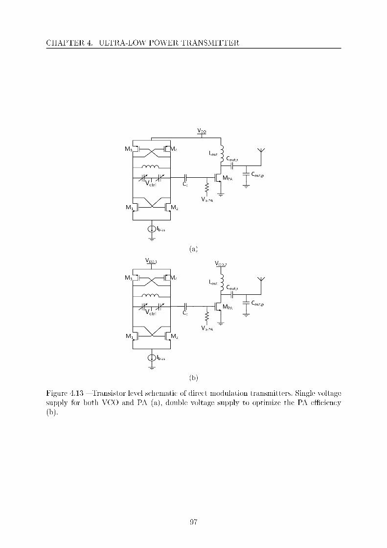
CHAPTER 4. ULTRA-LOW POWER TRANSMITTER
(a)
(b)
Figure 4.13 Transistor level schematic of direct modulation transmitters. Single voltagesupply for both VCO and PA (a), double voltage supply to optimize the PA eciency(b).
97

CHAPTER 4. ULTRA-LOW POWER TRANSMITTER
(a)
(b)
Figure 4.14 Bias point to perform class-C operation mode(a) typical voltage and currentwaveforms at the transistor drain(b) Biasing the transistor at voltage lower than thethreshold voltage permits to reduce the voltage and current overlapping period.
98
CHAPTER 4. ULTRA-LOW POWER TRANSMITTER
mum fundamental RF current (I1) value is achieved and its DC terms IDC consequently.Therefore the optimum load resistor can be founded from the Eq. 4.19. In this case a moregeneral form is preferable:
Ropti =V 2o,max
2P1,max
(4.24)
The dierence in the two equations comes from the fact that in Eq. 4.19 a maximumvoltage swing of VDD is supposed when the inductor works like a choke. The conditionwhere the inductor carries only DC current and bypasses all the AC currents into the loadis ωLchokeRL with a ratio of about 10. For example:
For a full drain voltage swing of 0.8 V and considering the targeted output voltageof -15 dBm (∼ 32 µW) the Ropti = 10 k Ω. Expressing the fundamental RF currentas:
I1 =Vo,maxRopti
(4.25)
The peak drain current Imax and the DC current are equals to:
Imax = 2πI1
1− cos(α2)
α− sin(α)= 2π
Vo,maxRopti
1− cos(α2)
α− sin(α)(4.26a)
IDC =Imax2π
2sin(α2)− αcos(α
2)
1− cos(α2)
(4.26b)
Taking a conduction angle of 150 Imax = 158 µA and the DC current is equal to42.75 µA. However a voltage amplitude equal to VDD would require Lchoke of 6.5µH which is impractical at 2.45 GHz even using o-chip components.
However for the designed PA the supply voltage of 0.8 V limits the swing to 0.4 V, becauseof the 1.2 V voltage forced by the MOS technology. This limitation aects the DC andthe RF current:
If Vo,max = 0.4 V the Ropti= 2.5 kΩ and for the same conduction angle of 150 thepeak RF current is Imax = 353 µ A and IDC = 95.5 µ A
The above considerations indicate that for the same output power, higher voltage swingat the output means higher load resistance but lower terms of RF current. Therefore thelimit imposed by the MOS technology forces the transistor to work with higher draincurrent thus the PA does not operate at peak eciency condition.However the downside of high load resistance is represented by poor MN eciency whenhigh conversion ratio is needed. In the case of Ropti = 10 kΩ and considering the standardvalue of 50 Ω for the antenna impedance the Eq. 4.23 shows a negative value of ηMN ,because the maximum quality factor QL achievable by the inductor is lower than the
quantity√
Ropti
Rs− 1. A practicable MN is possible when the Ropti = 2.5 kΩ, but a poor
ηMN = 42% demonstrates the drawback of high transformation ratio that signicantlyimpacts the overall performances. All these considerations are based on the fact that theinductor does not work like a choke and a practical value is possible.
The following items are some points to note in this case: The higher the ratio of impedance transformation the higher the Q of the transfor-
mation is. For a higher Q transformation, the intrinsic quality factor of the inductorin the network must be higher to minimize the losses in the network itself.
99

CHAPTER 4. ULTRA-LOW POWER TRANSMITTER
When the transformation ratio is very high, it is sometimes better to do the trans-formation in multiple steps, but this also degrades eciency of the network, andleads to more area.
A trade-o between the power consumption and the matching network design ap-pears when the power radiated is in the range of tens of µW. Fig. 4.16 shows thetrends of Ipeak and IDC for three dierent values of RL (2.5 kΩ, 1.25 kΩ, 0.60 kΩ)with the same output peak voltage of 0.4 V when the conduction angle moves from10 to 180. As illustrated, the peak currents increase when the load resistancedecreases in order to keep constant the output voltage swing, and thus also the DCcurrent increases consequently. Another important point is that the DC currentdecreases when the conduction angle decreases , while the peak current increasesforcing the transistor to work in current capability limit.
The simple L-matching network in Fig. 4.15 demonstrates that a non-integrable on-chip inductor is needed to transform higher impedance to 50 Ω.
Figure 4.15 Implementation of L-matching network to transform 50 Ω to the optimumload resistance of 2.5 kΩ. The large value of inductor makes dicult the integration ofthe passive element.
100
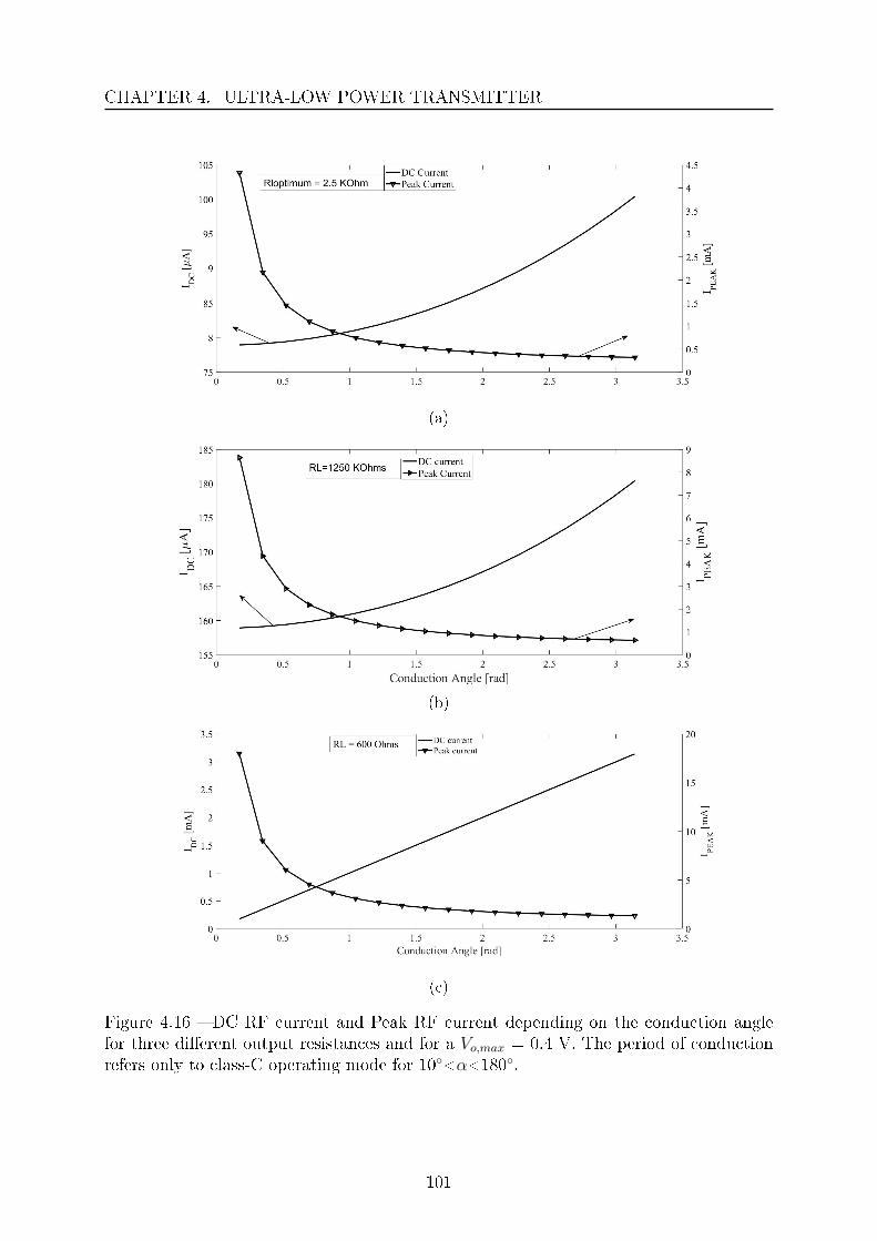
CHAPTER 4. ULTRA-LOW POWER TRANSMITTER
(a)
(b)
(c)
Figure 4.16 DC RF current and Peak RF current depending on the conduction anglefor three dierent output resistances and for a Vo,max = 0.4 V. The period of conductionrefers only to class-C operating mode for 10<α<180.
101

CHAPTER 4. ULTRA-LOW POWER TRANSMITTER
Figure 4.17 Implementation of L-matching and π-matching networks to transform 50Ω to the load resistance of 1.25 kΩ. A lower value of inductor is possible when a shuntcapacitor is added to the network.
Figure 4.18 DC RF load current and peak RF load current for RL = 1.25kΩ andVo,max = 0.282V depending on conduction angle .
Since the application requires low power consumption the PA should be designed withthe highest load resistance and low conduction angle to exploit the low range of DC RFcurrent. However as the main limiting factor is the implementation of matching network,higher power consumption has to be accepted due to a lower load resistance.To increase the network matching eciency above 50% and to make feasible its imple-mentation a load resistance of 1.25 kΩ is chosen. To present the correct impedance at thedrain of MOS transistor and to lter the unwanted harmonics a π-matching network isused to transform 50 Ω to 1.25 kΩ. This MN performs a better integrability respect to asimple L-matching topology. As seen from the Fig. 4.17 the inductor value scales downfrom 17 nH to 11 nH and also the capacitor increases from 257 fF to 450 fF, making theMN less susceptible to the capacitive parasites.Since the targeted power is equal to -15 dBm (∼ 32 µ W) and with the constraint ofRL the peak output voltage is equal to Vo,max =
√2RLPout = 0.282V . Once the load
resistance is set, to perform a class-C power amplier a conduction angle less than 180
has to be chosen. As explained previously the DC and the peak currents are aected whenthe conduction angle moves from 10 to 180. To limit the peak current below 1 mA, itis possible to observe the trend of IRF and IDC from the Fig. 4.18 and α = 150 (≈ 2.7rad) is chosen that conducts to a IDC ≈ 132 µA. The transistor is sized taking in accountthe MOS eciency and the required voltage swing at the gate. In fact this latter relates
102

CHAPTER 4. ULTRA-LOW POWER TRANSMITTER
Table 4.1 Drain current terms of PA MOSFET for dierent channel width, for the sameconduction angle and output power
ChannelWidth
Vg,DC Vg,RF IDC I1 PD
40 µm
310 mV 167 mV 319 µA 424 µA -12.8
290 mV 186 mV 298 µA 423 µA -12.8
270 mV 205 mV 281 µA 422 µA -12.8
250 mV 225 mV 272 µA 424 µA -12.8
30 µm
310 mV 159 mV 295 µA 424 µA -12.8
290 mV 176 mV 280 µA 423 µA -12.8
270 mV 194 mV 270 µA 422 µA -12.8
250 mV 212 mV 263.7 µA 421 µA -12.8
20 µm
310 mV 161 mV 274 µA 421 µA -12.8
290 mV 178 mV 267 µA 423 µA -12.8
270 mV 192.7 mV 260 µA 422 µA -12.8
250 mV 208 mV 255.7 µA 421 µA -12.8
directly to the bias current of the VCO. The MOS eciency can be expressed as
ηMOS =I1V1
2IDCVDD(4.27)
The Tab. 4.1 is made performing several simulation for dierent channel widths, at thesame output power and at the same conduction angle. The matching network is adaptedfor each size. The results show that the best MOS current ratio between the DC currentand the fundamental current is achieved for the smallest size of 20 µm.From the previously analysis the transistor channel width is 20 µm and it is biased at290 mV with an signal amplitude of 178 mV. In this case the PA is in moderate Class-Coperation, since that the threshold voltage is about 330 mV with a DC current of 267µA. The higher IDC , about two times higher than the value obtained from the previouslyanalysis, is due mainly to overcome the loss into the MN.Once all the PA characteristics are dened the design of the VCO is mainly focused toguarantee the optimum voltage swing at its output with good performances for currentconsumption and phase noise.
103
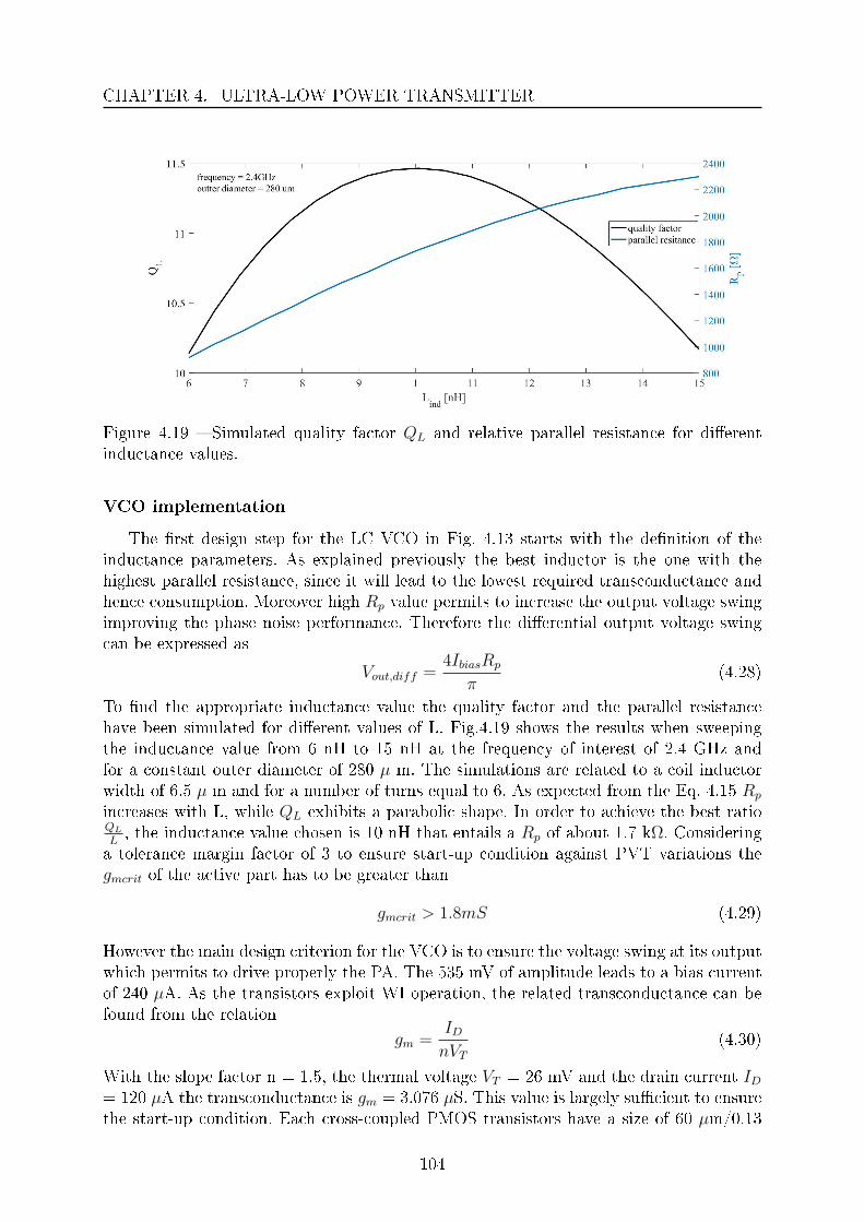
CHAPTER 4. ULTRA-LOW POWER TRANSMITTER
Figure 4.19 Simulated quality factor QL and relative parallel resistance for dierentinductance values.
VCO implementation
The rst design step for the LC VCO in Fig. 4.13 starts with the denition of theinductance parameters. As explained previously the best inductor is the one with thehighest parallel resistance, since it will lead to the lowest required transconductance andhence consumption. Moreover high Rp value permits to increase the output voltage swingimproving the phase noise performance. Therefore the dierential output voltage swingcan be expressed as
Vout,diff =4IbiasRp
π(4.28)
To nd the appropriate inductance value the quality factor and the parallel resistancehave been simulated for dierent values of L. Fig.4.19 shows the results when sweepingthe inductance value from 6 nH to 15 nH at the frequency of interest of 2.4 GHz andfor a constant outer diameter of 280 µ m. The simulations are related to a coil inductorwidth of 6.5 µ m and for a number of turns equal to 6. As expected from the Eq. 4.15 Rp
increases with L, while QL exhibits a parabolic shape. In order to achieve the best ratioQL
L, the inductance value chosen is 10 nH that entails a Rp of about 1.7 kΩ. Considering
a tolerance margin factor of 3 to ensure start-up condition against PVT variations thegmcrit of the active part has to be greater than
gmcrit > 1.8mS (4.29)
However the main design criterion for the VCO is to ensure the voltage swing at its outputwhich permits to drive properly the PA. The 535 mV of amplitude leads to a bias currentof 240 µA. As the transistors exploit WI operation, the related transconductance can befound from the relation
gm =IDnVT
(4.30)
With the slope factor n = 1.5, the thermal voltage VT = 26 mV and the drain current ID= 120 µA the transconductance is gm = 3.076 µS. This value is largely sucient to ensurethe start-up condition. Each cross-coupled PMOS transistors have a size of 60 µm/0.13
104

CHAPTER 4. ULTRA-LOW POWER TRANSMITTER
µm, while the NMOS pair has a size of 30 µm /0.13 µm. The tail transistor has a size of120 µm/ 0.13 µm.To tune the frequency of oscillation, two n-type accumulation mode MOS varactors areused. The variable capacitors are connected in parallel with the inductors. The tuningvoltage Vctrl is applied at the drain/source terminals. Some aspects have to be investigatedto reduce the gate resistance and the tank losses consequently. To increase the varactorquality factor, the channel length has to be kept at the minimum value, while an highnumber of gate ngers allows to decrease the gate resistance. However the width of eachngers is a compromise between the quality factor, the parasitics and the varactor size.
(a)
Figure 4.20 Varactor quality factor (a) and capacitance versus tuning voltage (b)
The Fig. 4.20 shows the varactor quality factor and the capacitance for a tuning voltagefrom 0 to 1 V. The relative frequency range varies from 2.34 GHz to 2.59 GHz (Fig. 4.21),and the tuning range achieved is about 10%. The Phase noise is shown in Fig. 4.22 andresults to be -115.2 dBc/Hz at 1 MHz from the carrier frequency. To evaluate the globalperformance of the designed VCO the accepted gure of merit FOM = 20 log(fosc
∆f) −
L(∆f) − 10 log(Pdiss,watt) is used, where fosc is the oscillation frequency, ∆f the oset
105
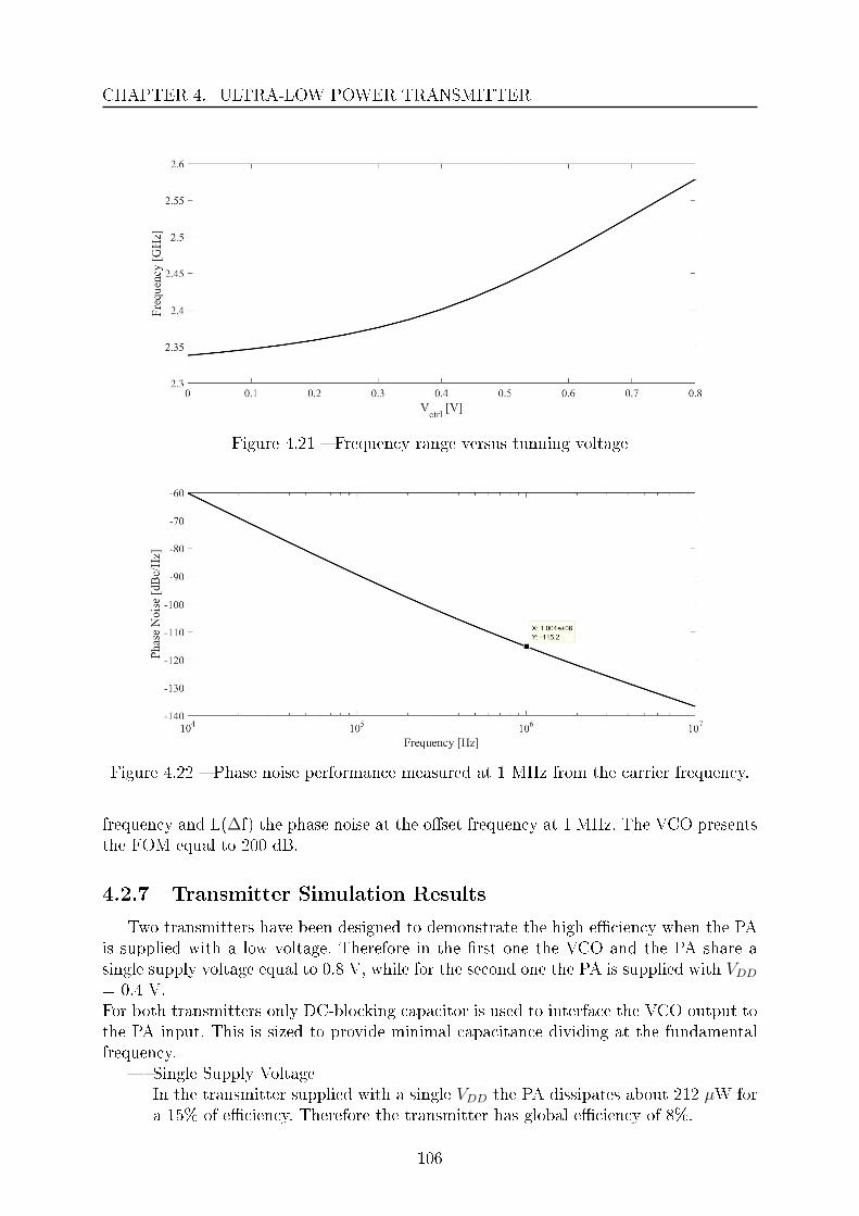
CHAPTER 4. ULTRA-LOW POWER TRANSMITTER
Figure 4.21 Frequency range versus tunning voltage
Figure 4.22 Phase noise performance measured at 1 MHz from the carrier frequency.
frequency and L(∆f) the phase noise at the oset frequency at 1 MHz. The VCO presentsthe FOM equal to 200 dB.
4.2.7 Transmitter Simulation Results
Two transmitters have been designed to demonstrate the high eciency when the PAis supplied with a low voltage. Therefore in the rst one the VCO and the PA share asingle supply voltage equal to 0.8 V, while for the second one the PA is supplied with VDD= 0.4 V.For both transmitters only DC-blocking capacitor is used to interface the VCO output tothe PA input. This is sized to provide minimal capacitance dividing at the fundamentalfrequency.
Single Supply VoltageIn the transmitter supplied with a single VDD the PA dissipates about 212 µW fora 15% of eciency. Therefore the transmitter has global eciency of 8%.
106
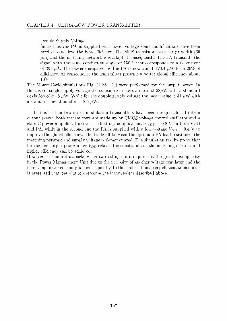
CHAPTER 4. ULTRA-LOW POWER TRANSMITTER
Double Supply VoltageSince that the PA is supplied with lower voltage some modications have beenneeded to achieve the best eciency. The MOS transistor has a larger width (60µm) and the matching network was adapted consequently. The PA transmits thesignal with the same conduction angle of 150 that corresponds to a dc currentof 301 µA. The power dissipated by the PA is now about 120.4 µW for a 26% ofeciency. As consequence the transmitter presents a better global eciency about10%.
The Monte Carlo simulations Fig. (4.23-4.24) were performed for the output power. Inthe case of single supply voltage the transmitter shows a mean of 28µW with a standarddeviation of σ=8 µW. While for the double supply voltage the mean value is 31 µW witha standard deviation of σ = 8.5 µW.
In this section two direct modulation transmitters have been designed for -15 dBmoutput power, both transmitters are made up by CMOS voltage control oscillator and aclass-C power amplier. However the rst one adopts a single VDD = 0.8 V for both VCOand PA, while in the second one the PA is supplied with a low voltage VDD = 0.4 V toimprove the global eciency. The trade-o between the optimum PA load resistance, thematching network and supply voltage is demonstrated. The simulation results prove thatfor the low output power a low VDD relaxes the constraints on the matching network andhigher eciency can be achieved.However the main drawbacks when two voltages are required is the greater complexityin the Power Management Unit due to the necessity of another voltage regulator and theincreasing power consumption consequently. In the next section a very ecient transmitteris presented that permits to overcome the inconvenient described above.
107

CHAPTER 4. ULTRA-LOW POWER TRANSMITTER
Figure 4.23 Monte Carlo simulation on the single supply voltage transmitter outputpower with 100 runs.
Figure 4.24 Monte Carlo simulation on the double supply voltage transmitter outputpower with 100 runs.
108

CHAPTER 4. ULTRA-LOW POWER TRANSMITTER
4.3 Current Reuse Transmitter
In the previous section the issues about the supply voltage and the matching networkat the PA output have been discussed. For very low output power a low VDD was pre-ferred to alleviate the MN and to improve the overall eciency. However in this work thetransmitter is supplied by the regulator described in the previous chapter, which presentsan output voltage of 1 V. Surely this voltage does not match very well with the targetedoutput power of -15 dBm. Therefore to eliminate the necessity of a second regulator tosupply an appropriate voltage for the power amplier a current reuse transmitter has beendesign.The idea is depicted in Fig. 4.25, where two possible topologies can be implementeddepending if the VCO or the PA is stacked on the top or on the bottom.
Figure 4.25 Block diagrams of current reuse transmitter. The two possible solutions arereported depending on the position of the VCO and the PA
Two main features can be founded in stacked architecture. The rst one is relatedto the total bias current that is recycled from the top block to the bottom one savingpower. The second one is related to the supply voltage, since it can be splitted in twooptimized voltages for each block. Therefore this architecture can solve the constraintsfor the targeted output power, where the supply voltage ratio between the VCO and thePA can be adjusted to reduce the required optimum resistance at the PA output.
109

CHAPTER 4. ULTRA-LOW POWER TRANSMITTER
4.3.1 Current Reuse VCO
The LC VCO implemented to generate the frequency carrier is a current reuse topology[YSCL05]. Fig. 4.26 shows the transistors implementation and the two operating states.The circuit is derived from a classical NMOS cross coupled oscillator, where one of thetwo NMOS transistors is replaced by a PMOS. Respect to the NMOS topology, the twotransistors are on at the same time in the rst half of oscillation period when the potentialat V out1 is high. Therefore a direct path is created from the supply voltage and the groundthrough the transistors and the energy is stocked in the inductor. In the second half period,when Vout1 is at low level, the (N- and PMOS) transistors are o and current ows throughthe capacitors. It is interesting to highlight that in the rst half period the oscillator isin the voltage limited operation where the amplitude of the oscillation can extend up toVDD. In the second state no limitation is present and the peak oscillation can exceed thesupply voltage.Another remarkable point is that the same feature of CMOS cross coupledVCO can be founded in the current reuse topology. Since the transistors switch on at thesame time the transconductance presented is twice of that NMOS cross coupled topologyfor the same bias current. Moreover the absence of the common source node avoids noiseaddition from the second harmonic term and improve phase noise performance due to alow icker noise of the PMOS transistor.However without some modications, current reuse oscillator is not suitable for fullydierential applications since that the output voltage swing is not balanced. The reasoncomes from the two dierent operating modes, in the rst and in the second half period,and from the large drop in the dynamic current. To re-equalize the output a bias resistorcan be added between the NMOS source and the ground, to force the VCO to operate inlimited current mode in both periods.However to work properly and to ensure start-up condition over PVT variations, thestacked topology has to be supplied with a voltage greater than the sum of PMOS andNMOS threshold voltage. For the RF transistors available in the design kit, VDD shouldbe higher than 0.85 V. At this point it seems clear that the 1 V of voltage supply for thetransmitter architecture is not suitable to ensure sucient voltage headroom for the PAand the VCO at the same time. To allow start-up condition also for low supply voltagethe NMOS transistor can be biased separately to provide minimum negative resistance tosustain the oscillation [TGF12]. The Fig. 4.27 depicts the modied current reuse VCO,where the NMOS gate transistor is AC-coupled via Cdec to the node Y, and the Rbias
represents the bias resistance. An ac-ground capacitor CAC is needed to ground all highfrequencies voltage bias components. However the ac-coupling capacitor and the biasresistor have to be properly sized to provide high enough start-up gain.
110

CHAPTER 4. ULTRA-LOW POWER TRANSMITTER
Figure 4.26 LC current reuse oscillator schematic.The two operating states are alsoillustrated for the two dierent oscillation periods.
111

CHAPTER 4. ULTRA-LOW POWER TRANSMITTER
Figure 4.27 Modied current reuse VCO for low supply voltage.
From the analysis done in [TGF12] the impedance seen at the node Y is expressed as
ZY = (1
Rbias,Y
+ |Av|gmn + gmp − |AV |gmngmpRp)−1 (4.31)
where Rbias,Y is the equivalent bias resistance seen at node Y to the ground, Av=VXVY
isthe voltage divider ratio between the node X and Y, Rp is the parasitic resistance of thetank. Since ZY has to be negative and high enough to ensure start-up condition, Av hasto be close to one. Considering the gate-source parasitic capacitance of NMOS transistorCgs,nmos the decoupling capacitor Cdec should be larger than the parasitic capacitance toensure high voltage divider ratio.If Cdec Cgs,nmos Rbias,y ≈ Rbias, therefore to not degrade the tank quality factor Rbias hasto be higher than Rp. However high value can degrade the phase noise performance due tohigher thermal noise. Fig. 4.29 conrms this hypothesis, high value of Rbias correspondsto worst PN Rbias = 4.5 kΩ can represent a good trade-o. Fig. 4.28 plots AV versus Cdec.It is worth noting that the voltage divider ration does not change signicantly for Cdec >750 fF thus this value has been chosen.Also for the current reuse oscillator the frequency tuning is ensured by two NMOS var-actors and a 9 nH inductor with a quality factor of 12 at the oscillation frequency. Fig.4.30 shows the phase noise at 1 MHz from the carrier frequency when the supply voltagemoves from 0.6 V to 1 V. Fig. 4.31 shows the FoM and the power dissipation on the samesupply voltage range.In the next section the current reuse transmitter is presented, where the power amplierstage is stacked on top of the VCO.
112

CHAPTER 4. ULTRA-LOW POWER TRANSMITTER
Figure 4.28 Voltage divider ratio versus the decoupling capacitor Cdec
Figure 4.29 Phase noise performance measured at 1 MHz oset from the carrier frequencyversus the bias resistance.
113
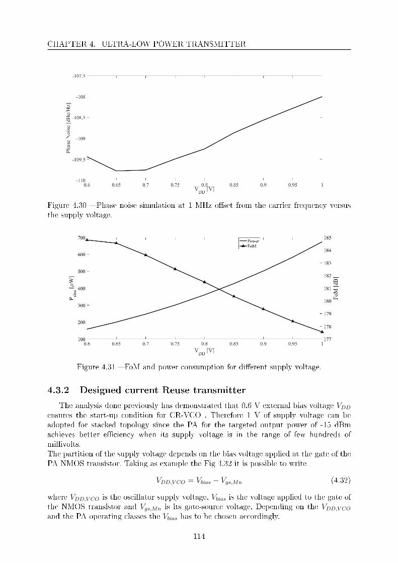
CHAPTER 4. ULTRA-LOW POWER TRANSMITTER
Figure 4.30 Phase noise simulation at 1 MHz oset from the carrier frequency versusthe supply voltage.
Figure 4.31 FoM and power consumption for dierent supply voltage.
4.3.2 Designed current Reuse transmitter
The analysis done previously has demonstrated that 0.6 V external bias voltage VDDensures the start-up condition for CR-VCO . Therefore 1 V of supply voltage can beadopted for stacked topology since the PA for the targeted output power of -15 dBmachieves better eciency when its supply voltage is in the range of few hundreds ofmillivolts.The partition of the supply voltage depends on the bias voltage applied at the gate of thePA NMOS transistor. Taking as example the Fig 4.32 it is possible to write
VDD,V CO = Vbias − Vgs,Mn (4.32)
where VDD,V CO is the oscillator supply voltage, Vbias is the voltage applied to the gate ofthe NMOS transistor and Vgs,Mn is its gate-source voltage. Depending on the VDD,V COand the PA operating classes the Vbias has to be chosen accordingly.
114

CHAPTER 4. ULTRA-LOW POWER TRANSMITTER
Figure 4.32 Supply voltage trend.
Figure 4.33 Trend of the voltage at the common node P.
From the study carried out on about the power amplier in classical transmitter topologyand observing the trend of the CR-VCO FoM, the supply voltage about 0.65 V is chosenfor the oscillator thus the remaining 0.35 V for the PA is an appropriate value for theM.N. trade-o.The complete transistor level schematic is depicted in Fig. 4.34 where the PA is stackedon top to have the possibility to explore all PA operating classes and a better control onthe output power. To implement current reuse topology and to shunt all AC componentsavoiding possible high frequency loop and providing a virtual VDD to the VCO, a shuntcapacitor of 20 pF is inserted at the PA and VCO common node. In the Fig. 4.33 thetrend of the voltage at node P over the time is depicted, since the VCO and the PA aretwo large signal circuits Vp achieves nal value when the oscillation is settled.
115

CHAPTER 4. ULTRA-LOW POWER TRANSMITTER
Figure 4.34 Transistor level schematic of Current Reuse transmitter.
116

CHAPTER 4. ULTRA-LOW POWER TRANSMITTER
Table 4.2 Devices size for the designed transmitter.
Value
Lout 7 nH
Cout,s 450 fF
Cout,p 1 pF
MPA50
0,13µmµm
L 10 nH
Mp60
0,13µmµm
MN40
0,13µmµm
C 600 fF
Vbias 400 mV
Cby−pass 20 pF
Figure 4.35 Voltage and Current transient at the MPA drain.
Once the supply voltages for the two blocks are xed the design methodology is asfollow:
The transmitter bias current is xed by the targeted output power, by the feasibleload resistance (as explained in the previously section) and by the PA operatingclass with the Eq. 4.25-4.26.
With the current value the VCO tank inductor is chosen to have sucient voltageswing at the MPA gate, in order to set the conduction angle properly. The relationcan be seen from the Eq. 4.28.
The relative parasitic inductor resistance xes the minimum gm,crit necessary tosustain the oscillation. The gm,crit is assured setting the bias voltage of CR-VCOVbias and sizing the transistors Mp and MN .
117

CHAPTER 4. ULTRA-LOW POWER TRANSMITTER
Figure 4.36 Phase noise simulated at 1 Mhz from the carrier frequency.
Figure 4.37 MonteCarlo simulation performed over output power.
The Tab 4.2 summarizes the nal values for the transmitter devices. The bias currentneeded to transmit -15 dBm is about 310 µA for a total power dissipation of 310 µW. TheFig 4.35 shows the transient behavior of current and voltage drain of the power amplierwhile the Fig. 4.36 shows the phase noise at 1 MHz from the carrier frequency. The currentreuse transmitter exhibits a total power eciency of 10.5 %.Fig 4.37 shows the Monte Carlo simulation performed for the output power. The trans-mitter shows a mean of 32 µW with a standard deviation of σ = 4 µW.
118

CHAPTER 4. ULTRA-LOW POWER TRANSMITTER
4.4 Conclusion
In this chapter a design methodology for transmitter in short communication distancehas been presented. The output power of -15 dBm entails that the approach should bedierent from the traditional approach adopted to design long distance transmitter. Toachieve low power consumption a direct modulation scheme has been adopted to reducethe number of blocks needed for the transmission.In the rst part of the chapter two classical transmitters have been presented where thevoltage control oscillator and the power amplier are cascaded. The discussion mainlyfocused on the diculty to transform the preferably high load resistance, when thepower transmitted is about few tens of micro-watt, to the standard 50 Ω input antennaimpedance. The trade-o between the supply voltage, the bias current and matching net-work eciency have been demonstrated. To show the advantages when the PA is suppliedby a lower voltage two transmitters have been designed. In the rst one the VCO andthe PA share the same supply voltage of 0.8 V, in the second one the VCO maintains thesame voltage while the PA is supplied with a voltage of 0.4 V. However a double supplyvoltage requires another voltage regulator, that means more power dissipated and morecomplex system.To circumnavigate this problem, a current-reuse transmitter has been proposed where theVCO and the PA are stacked and the bias current is recycled from the top circuit to thebottom one. The possibility to distribute a single supply voltage in two optimized voltageone for each block oers several degree of freedom for targeted output power, phase noiseand power consumption. Moreover for this topology only one voltage regulator is neededreducing the complexity of the system.
119

Chapter 5
Conclusions
This work investigates the design of ultra-low power circuits for Harvesting applica-tions, in particular LDO voltage regulator and transmission part are involved in the study.To address the design, the rst part of dissertation presents the low-power techniques atthree dierent levels: transistors level, circuit level and system level.In addition the main sources of energy Harvesting are presented outlining the energyavailable at their output and the level of integration. As the application targeted is thepossibility to replace battery with EH source in wireless sensor networks in order to extendthe operation lifetime, some system aspects are presented. From the networks architectureto the link budget, data-rate and energy management aspects. These lasts are fundamen-tal aspects to take into account to give the circuit specications. Moreover the equationto estimate the optimum DC for the lowest energy consumption is given.Chapter 3 shows that to reduce the regulator power consumption even beyond to use theMosfet transistors in Moderate Inversion, the better way to reduce the energy budget isto adapt the quiescent current to the load current of the LDO voltage regulator. With theclass-AB Error Amplier and an adaptively bias approach also the transient response isimproved. Therefore the LDO exhibits a quiescent current that spans from 560 nA to 1.8µA when Iload moves from 1 µA to 1mA. While the time response is halved. The regulatoris designed to transform a variable input voltage of 1.2 V in a stable output voltage of 1V.Two architectures for the transmission part are proposed in chapter 4: a classical cascadedtopology VCO-PA and a current reuse transmitter. As the radiated power is in the rangeof some µW, there is a severe trade-o between the matching network eciency and thepower amplier supply voltage. The achieve a global power eciency about 10% the os-cillator and the amplier, in cascaded topology, are supplied with two dedicated voltagesof 0.8 V and 0.4 V. To avoid two voltage regulators which increases system complexity,the current reuse permits to tune unique voltage supply between the VCO and the PAalleviating the design constraints for the matching network. Therefore a comparable e-ciency of 10.5% is obtained. Moreover Montecarlo simulations demonstrate that currentreuse topology is more robust against PVT variations.
Perspective
To validate the obtained simulation results, the circuits realization and its measure-ments are the obvious steps to do consequently. More interesting would be the possibility
120

CHAPTER 5. CONCLUSIONS
to test the circuits in a more complex system, where the signal modulation incoming fromthe analog-to-digital convert.As the regulator presents important dependence PVT variations, an additional circuit toadjust the error amplier bias current could represent a solution to mitigate these eects.From the transmission side, to improve the spectrum eciency of the signal radiated alow-power FSK modulation could be easily implemented.
121

Appendix A
Drain current calculation in class AB
Error Amplier
Figure A.1 FVF cell with cascode Pmos transistor
Since that the transistors M1, M2, MA1, MA2 operate in sub-threshold the drain cur-rents are expressed as
IDS,M1 = ID0,M1(W
L)M1 exp
(Vgs,M1 − VTH
nVt
)(A.1a)
IDS,M2 = ID0,M2(W
L)M2 exp
(Vgs,M2 − VTH
nVt
)(A.1b)
IDS,MA1 = ID0,MA1(W
L)MA1 exp
(Vgs,MA1 − VTH
nVt
)(A.1c)
IDS,MA2 = ID0,MA2(W
L)MA2 exp
(Vgs,MA2 − VTH
nVt
)(A.1d)
The gate source voltage of M1 and M2 is equal to
Vgs,M1 = V −in − Vs,M1 = V +in − Vs,MA1 (A.2a)
Vgs,M2 = V +in − Vs,M2 = V +
in − Vs,MA2 (A.2b)
122

APPENDIX A. DRAIN CURRENT CALCULATION IN CLASS AB ERRORAMPLIFIER
From Eq. A1c and A1d the source voltages VsA1 and VsA2 are equal to
Vs,MA1 = − log
(IMA1
ID0,MA1(WL
)MA1
)ηVT + V +
in − VTH (A.3a)
Vs,MA2 = − log
(IMA2
ID0,MA2(WL
)MA2
)ηVT + V 1
in − VTH (A.3b)
Substituting eq A3a and A3b in A2a and A2b, and then in the A1a and A1b the draincurrent of transistors M1 and M2 is equal
ID1 = IDO
(W
L
)M1
exp
[log
(IDA1
IDO(WL
)MA1
)− Vdiff
1
VTn
](A.4a)
ID2 = IDO
(W
L
)M2
exp
[log
(IDA2
IDO(WL
)MA2
)+ Vdiff
1
VTn
](A.4b)
123

Bibliography
[Ben09] A. Bensky. Fundamentals of rf system design and application second edi-tion. In Short Range Wireless Communication, 2009.
[Bin07] D. M. Binkley. Tradeos and optimization in analog cmos design. In 200714th International Conference on Mixed Design of Integrated Circuits andSystems, pages 4760, June 2007.
[CS90] L. G. A. Callewaert and W. M. C. Sansen. Class ab cmos ampliers withhigh eciency. IEEE Journal of Solid-State Circuits, 25(3):684691, Jun1990.
[DvdZBK11] R. Dutta, R. v. d. Zee, M. J. Bentum, and A. B. J. Kokkeler. Choos-ing optimum noise gure and data rate in wireless sensor network radiotransceivers. In 2011 IEEE International Conference on Communications(ICC), pages 15, June 2011.
[ea06] Y. H. Chee et al. Ultra low pawer transmitters for wireless sensor networks.In Thesis Univ of California, Berkley, 2006.
[EC15] C. Enz and M. A. Chalkiadaki. Nanoscale mosfet modeling for low-powerrf design using the inversion coecient. In 2015 Asia-Pacic MicrowaveConference (APMC), volume 1, pages 13, Dec 2015.
[ECC17] Electronic Communication Committeed ECC. In ERC recommendationsfor short wireless devices, May 2017.
[ESY05] C. Enz, N. Scolari, and U. Yodprasit. Ultra low-power radio design forwireless sensor networks. In 2005 IEEE International Wkshp on Radio-Frequency Integration Technology: Integrated Circuits for Wideband CommWireless Sensor Networks, pages 117, Nov 2005.
[EV96] C. C. Enz and E. A. Vittoz. Cmos low-power analog circuit design. InEmerging Technologies: Designing Low Power Digital Systems, pages 79133, 1996.
[FF14] W. Fu and A. Fayed. A self-regulated 588 mhz buck regulator with on-chippassives and circuit stung in 65nm. pages 338341, Aug 2014.
[GL10] J. Guo and K. N. Leung. A 6- µ w chip-area-ecient output-capacitorlessldo in 90-nm cmos technology. IEEE Journal of Solid-State Circuits,45(9):18961905, Sept 2010.
[GMPP15] A. D. Grasso, D. Marano, G. Palumbo, and S. Pennisi. Design methodologyof subthreshold three-stage cmos otas suitable for ultra-low-power low-areaand high driving capability. IEEE Transactions on Circuits and SystemsI: Regular Papers, 62(6):14531462, June 2015.
124

BIBLIOGRAPHY
[GPP08] A. D. Grasso, G. Palumbo, and S. Pennisi. Comparison of the frequencycompensation techniques for cmos two-stage miller otas. IEEE Transac-tions on Circuits and Systems II: Express Briefs, 55(11):10991103, Nov2008.
[GPS12] G. Giustolisi, G. Palumbo, and E. Spitale. Robust miller compensationwith current ampliers applied to ldo voltage regulators. IEEE Transac-tions on Circuits and Systems I: Regular Papers, 59(9):18801893, Sept2012.
[GRF10] A. Garimella, M. W. Rashid, and P. M. Furth. Reverse nested millercompensation using current buers in a three-stage ldo. IEEE Transactionson Circuits and Systems II: Express Briefs, 57(4):250254, April 2010.
[HHY12] T. C. Huang, C. Y. Hsieh, Y. Y. Yang, Y. H. Lee, Y. C. Kang, K. H.Chen, C. C. Huang, Y. H. Lin, and M. W. Lee. A battery-free 217 nwstatic control power buck converter for wireless rf energy harvesting withα -calibrated dynamic on/o time and adaptive phase lead control. IEEEJournal of Solid-State Circuits, 47(4):852862, April 2012.
[HLL99] A. Hajimiri, S. Limotyrakis, and T. H. Lee. Jitter and phase noise in ringoscillators. IEEE Journal of Solid-State Circuits, 34(6):790804, Jun 1999.
[HM10] E. N. Y. Ho and P. K. T. Mok. A capacitor-less cmos active feedbacklow-dropout regulator with slew-rate enhancement for portable on-chipapplication. IEEE Transactions on Circuits and Systems II: Express Briefs,57(2):8084, Feb 2010.
[HP06] Y. Han and D. J. Perreault. Analysis and design of high eciency matchingnetworks. IEEE Transactions on Power Electronics, 21(5):14841491, Sept2006.
[HUKN10] T. Hirose, K. Ueno, N. Kuroki, and M. Numa. A cmos bandgap and sub-bandgap voltage reference circuits for nanowatt power lsis. In 2010 IEEEAsian Solid-State Circuits Conference, pages 14, Nov 2010.
[JLBS15] S. Jeong, I. Lee, D. Blaauw, and D. Sylvester. A 5.8 nw cmos wake-uptimer for ultra-low-power wireless applications. IEEE Journal of Solid-State Circuits, 50(8):17541763, Aug 2015.
[KBA16] R. Karli, A. Bouchalkha, and K. Alhammadi. Power consumption andbattery life study of a two-node wireless sensor system. In 2016 5th In-ternational Conference on Electronic Devices, Systems and Applications(ICEDSA), pages 14, Dec 2016.
[KBW12] W. Kim, D. Brooks, and G. Y. Wei. A fully-integrated 3-level dc-dc con-verter for nanosecond-scale dvfs. IEEE Journal of Solid-State Circuits,47(1):206219, Jan 2012.
[KCSN14] K. Kim, J. Choi, M. Seo, and S. Nam. 500 mhz ook transmitter with 22pj/bit, 38.4current combining. IEEE Microwave and Wireless ComponentsLetters, 24(6):424426, June 2014.
[KM14] K. Keikhosravy and S. Mirabbasi. A 0.13- µm cmos low-power capacitor-less ldo regulator using bulk-modulation technique. IEEE Transactions onCircuits and Systems I: Regular Papers, 61(11):31053114, Nov 2014.
125

BIBLIOGRAPHY
[KPL17] S. J. Kim, C. S. Park, and S. G. Lee. A 2.4-ghz ternary sequence spreadspectrum ook transceiver for reliable and ultra-low power sensor networkapplications. IEEE Transactions on Circuits and Systems I: Regular Pa-pers, 64(11):29762987, Nov 2017.
[LARG07] E. Lefeuvre, D. Audigier, C. Richard, and D. Guyomar. Buck-boost con-verter for sensorless power optimization of piezoelectric energy harvester.IEEE Transactions on Power Electronics, 22(5):20182025, Sept 2007.
[LBvdH14] Y. H. Liu, A. Ba, J. H. C. van den Heuvel, K. Philips, G. Dolmans, andH. de Groot. 9.5 a 1.2nj/b 2.4ghz receiver with a sliding-if phase-to-digitalconverter for wireless personal/body-area networks. In 2014 IEEE Interna-tional Solid-State Circuits Conference Digest of Technical Papers (ISSCC),pages 166167, Feb 2014.
[LBW15] Y. H. Liu, C. Bachmann, X. Wang, Y. Zhang, A. Ba, B. Busze,M. Ding, P. Harpe, G. J. van Schaik, G. Selimis, H. Giesen, J. Gloude-mans, A. Sbai, L. Huang, H. Kato, G. Dolmans, K. Philips, andH. de Groot. 13.2 a 3.7mw-rx 4.4mw-tx fully integrated bluetooth low-energy/ieee802.15.4/proprietary soc with an adpll-based fast frequency o-set compensation in 40nm cmos. In 2015 IEEE International Solid-StateCircuits Conference - (ISSCC) Digest of Technical Papers, pages 13, Feb2015.
[LCF09] C. Li, M. Crepaldi, and J. R. Fernandes. Power consumption trade-os inshort-distance wireless transceivers for sensor nodes. pages 189193, Sept2009.
[LGZ15] G. Li, J. Guo, Y. Zheng, M. Huang, and D. Chen. Cascoded ipped voltagefollower based output-capacitorless low-dropout regulator for socs. 201528th IEEE International System-on-Chip Conference (SOCC), pages 368373, Sept 2015.
[LH00] T. H. Lee and A. Hajimiri. Oscillator phase noise: a tutorial. IEEE Journalof Solid-State Circuits, 35(3):326336, March 2000.
[LHVY07] J. Lee, G. Hatcher, L. Vandenberghe, and C. K. K. Yang. Evaluation offully-integrated switching regulators for cmos process technologies. IEEETransactions on Very Large Scale Integration (VLSI) Systems, 15(9):10171027, Sept 2007.
[LMBRAC05] A. J. Lopez-Martin, S. Baswa, Jaime Ramirez-Angulo, and R. G. Carvajal.Low-voltage super class ab cmos ota cells with very high slew rate andpower eciency. IEEE Journal of Solid-State Circuits, 40(5):10681077,May 2005.
[LML07] S. K. Lau, P. K. T. Mok, and K. N. Leung. A low-dropout regulator forsoc with q -reduction. IEEE Journal of Solid-State Circuits, 42(3):658664,March 2007.
[LRWW05] E. Y. A. Lin, J. M. Rabaey, S. Wiethoelter, and A. Wolisz. Receiverinitiated rendezvous schemes for sensor networks. In GLOBECOM '05.IEEE Global Telecommunications Conference, 2005., volume 5, pages 6pp.3122, Dec 2005.
126

BIBLIOGRAPHY
[LSS15] X. Liu and E. Sánchez-Sinencio. An 86system with hysteresis regulationand time-domain mppt for iot smart nodes. IEEE Journal of Solid-StateCircuits, 50(6):14241437, June 2015.
[MA08] A. Mazzanti and P. Andreani. Class-c harmonic cmos vcos, with a generalresult on phase noise. IEEE Journal of Solid-State Circuits, 43(12):27162729, Dec 2008.
[MBL13] P. P. Mercier, S. Bandyopadhyay, A. C. Lysaght, K. M. Stankovic, and A. P.Chandrakasan. A 78 pw 1 b/s 2.4 ghz radio transmitter for near-zero-powersensing applications. In 2013 Proceedings of the ESSCIRC (ESSCIRC),pages 133136, Sept 2013.
[MBT13] B. Mishra, C. Botteron, G. Tasselli, C. Robert, and P. A. Farine. A sub-µapower management circuit in 0.18 µm cmos for energy harvesters. 2013Design, Automation Test in Europe Conference Exhibition (DATE), pages11971202, March 2013.
[MKB14] O. E. Mattia, H. Klimach, and S. Bampi. 0.9 v, 5 nw, 9 ppm/oc resistorlesssub-bandgap voltage reference in 0.18 µm cmos. In 2014 IEEE 5th LatinAmerican Symposium on Circuits and Systems, pages 14, Feb 2014.
[MPW17] I. Mahbub, S. A. Pullano, H. Wang, S. K. Islam, A. S. Fiorillo, G. To, andM. R. Mahfouz. A low-power wireless piezoelectric sensor-based respira-tion monitoring system realized in cmos process. IEEE Sensors Journal,17(6):18581864, March 2017.
[OST16] H. Okuni, A. Sai, T. T. Ta, S. Kondo, T. Tokairin, M. Furuta, andT. Itakura. 26.1 a 5.5mw adpll-based receiver with hybrid-loop interferencerejection for ble application in 65nm cmos. In 2016 IEEE InternationalSolid-State Circuits Conference (ISSCC), pages 436437, Jan 2016.
[PCFP14] G. Papotto, F. Carrara, A. Finocchiaro, and G. Palmisano. A 90-nmcmos 5-mbps crystal-less rf-powered transceiver for wireless sensor networknodes. IEEE Journal of Solid-State Circuits, 49(2):335346, Feb 2014.
[PO11] J. Pandey and B. P. Otis. A sub-100 µ w mics/ism band transmitterbased on injection-locking and frequency multiplication. IEEE Journal ofSolid-State Circuits, 46(5):10491058, May 2011.
[POSM14] C. J. Park, M. Onabajo, and J. Silva-Martinez. External capacitor-lesslow drop-out regulator with 25 db superior power supply rejection in the0.4-4 Mhz range. IEEE Journal of Solid-State Circuits, 49(2):486501, Feb2014.
[PPA15] J. Prummel, M. Papamichail, M. Ancis, J. Willms, R. Todi, W. Aartsen,W. Kruiskamp, J. Haanstra, E. Opbroek, S. Rievers, P. Seesink, H. Wo-ering, and C. Smit. 13.3 a 10mw bluetooth low-energy transceiver withon-chip matching. In 2015 IEEE International Solid-State Circuits Con-ference - (ISSCC) Digest of Technical Papers, pages 13, Feb 2015.
[Raz]
[Raz99] ransmitter architectures and circuits. In Proceedings of the IEEE 1999Custom Integrated Circuits Conference (Cat. No.99CH36327), pages 197204, 1999.
127

BIBLIOGRAPHY
[RGTSS12] M. A. Rojas-González, J. Torres, and E. Sánchez-Sinencio. Design of afully-integrated buck voltage regulator using standard cmos technology.pages 14, Feb 2012.
[RM10] M. Raju and M.Grazier. Ulp meets energy harvesting: A game-changingcombination for design enginners. In Texas Instrument, White Paper, 2010.
[RM17] D. Rozgi¢ and D. Markovi¢. A miniaturized 0.78-mw/cm2 autonomousthermoelectric energy-harvesting platform for biomedical sensors. IEEETransactions on Biomedical Circuits and Systems, PP(99):111, 2017.
[SGMK15] S. Singhal, N. Gaur, A. Mehra, and P. Kumar. Analysis and comparison ofleakage power reduction techniques in cmos circuits. In 2015 2nd Interna-tional Conference on Signal Processing and Integrated Networks (SPIN),pages 936944, Feb 2015.
[SH06] A. Shameli and P. Heydari. Ultra-low power rc design using moderatelyinverted mosfets: an analytical/experimental study. In IEEE Radio Fre-quency Integrated Circuits (RFIC) Symposium, 2006, pages 4 pp., June2006.
[TGF12] M. Taghivand, M. Ghahramani, and M. P. Flynn. A low voltage sub 300µw 2.5Ghz current reuse vco. In 2012 IEEE Asian Solid State CircuitsConference (A-SSCC), pages 369372, Nov 2012.
[TLHL14] J. Tan, W. S. Liew, C. H. Heng, and Y. Lian. A 2.4 Ghz ulp recongurableasymmetric transceiver for single-chip wireless neural recording ic. IEEETransactions on Biomedical Circuits and Systems, 8(4):497509, Aug 2014.
[TRE15a] R. Thirunarayanan, D. Rueux, and C. Enz. Reducing energy dissipationin ulp systems: Pll-free fbar-based fast startup transmitters. IEEE Transac-tions on Microwave Theory and Techniques, 63(4):11101117, April 2015.
[TRE15b] R. Thirunarayanan, D. Rueux, and C. Enz. Reducing energy dissipationin ulp systems: Pll-free fbar-based fast startup transmitters. IEEE Transac-tions on Microwave Theory and Techniques, 63(4):11101117, April 2015.
[TSM15] T. Taris, A. H. M. Shirazi, and S. Mirabbasi. Design of low power cmosrf building blocks. In 2015 Asia-Pacic Microwave Conference (APMC),volume 1, pages 13, Dec 2015.
[TSW15] K. Tien, N. Sturcken, N. Wang, J. w. Nah, B. Dang, E. O'Sullivan,P. Andry, M. Petracca, L. P. Carloni, W. Gallagher, and K. Shepard. An82on-chip magnetic inductors. In 2015 Symposium on VLSI Circuits (VLSICircuits), pages C192C193, June 2015.
[TTKS14] W. Y. Toh, Y. K. Tan, W. S. Koh, and L. Siek. Autonomous wear-able sensor nodes with exible energy harvesting. IEEE Sensors Journal,14(7):22992306, July 2014.
[UHAA09] K. Ueno, T. Hirose, T. Asai, and Y. Amemiya. A 300 nw, 15 ppm/ c, 20ppm/v cmos voltage reference circuit consisting of subthreshold mosfets.IEEE Journal of Solid-State Circuits, 44(7):20472054, July 2009.
[Van15] V. N. R. Vanukuru. High- Q inductors utilizing thick metals and dense-tapered spirals. IEEE Transactions on Electron Devices, 62(9):30953099,Sept 2015.
128

BIBLIOGRAPHY
[VHH11a] M. Vidojkovic, X. Huang, P. Harpe, S. Rampu, C. Zhou, L. Huang,J. van de Molengraft, K. Imamura, B. Busze, F. Bouwens, M. Konijnen-burg, J. Santana, A. Breeschoten, J. Huisken, K. Philips, G. Dolmans,and H. de Groot. A 2.4 ghz ulp ook single-chip transceiver for health-care applications. IEEE Transactions on Biomedical Circuits and Systems,5(6):523534, Dec 2011.
[VHH11b] M. Vidojkovic, X. Huang, P. Harpe, S. Rampu, C. Zhou, L. Huang,J. van de Molengraft, K. Imamura, B. Busze, F. Bouwens, M. Konijnen-burg, J. Santana, A. Breeschoten, J. Huisken, K. Philips, G. Dolmans,and H. de Groot. A 2.4 ghz ulp ook single-chip transceiver for health-care applications. IEEE Transactions on Biomedical Circuits and Systems,5(6):523534, Dec 2011.
[VHH11c] M. Vidojkovic, X. Huang, P. Harpe, S. Rampu, C. Zhou, L. Huang,J. van de Molengraft, K. Imamura, B. Busze, F. Bouwens, M. Konijnen-burg, J. Santana, A. Breeschoten, J. Huisken, K. Philips, G. Dolmans,and H. de Groot. A 2.4 ghz ulp ook single-chip transceiver for health-care applications. IEEE Transactions on Biomedical Circuits and Systems,5(6):523534, Dec 2011.
[VI07] G. De Vita and G. Iannaccone. A sub-1-v, 10 ppm/ circic, nanopower volt-age reference generator. IEEE Journal of Solid-State Circuits, 42(7):15361542, July 2007.
[VN78] E. Vittoz and O. Neyroud. A low-voltage cmos bandgap reference. InESSCIRC 78: 4th European Solid State Circuits Conference - Digest ofTechnical Papers, pages 139141, Sept 1978.
[WH08] J. Wibben and R. Harjani. A high-eciency dc-dc converter using 2 nhintegrated inductors. IEEE Journal of Solid-State Circuits, 43(4):844854,April 2008.
[WKvL01] P. H. Woerlee, M. J. Knitel, R. van Langevelde, D. B. M. Klaassen, L. F.Tiemeijer, A. J. Scholten, and A. T. A. Zegers van Duijnhoven. Rf-cmosperformance trends. IEEE Transactions on Electron Devices, 48(8):17761782, Aug 2001.
[WTM10] P. Y. Wu, S. Y. S. Tsui, and P. K. T. Mok. Area- and power-ecient mono-lithic buck converters with pseudo-type iii compensation. IEEE Journal ofSolid-State Circuits, 45(8):14461455, Aug 2010.
[WTY11] Z. G. Wan, Y. K. Tan, and C. Yuen. Review on energy harvesting andenergy management for sustainable wireless sensor networks. In 2011 IEEE13th International Conference on Communication Technology, pages 362367, Sept 2011.
[YSCL05] Seok-Ju Yun, So-Bong Shin, Hyung-Chul Choi, and Sang-Gug Lee. A 1mwcurrent-reuse cmos dierential lc-vco with low phase noise. In ISSCC.2005 IEEE International Digest of Technical Papers. Solid-State CircuitsConference, 2005., pages 540616 Vol. 1, Feb 2005.
[ZG12] M. Zargham and P. G. Gulak. Fully-integrated, power-ecient regulatorand bandgap circuits for wireless-powered biomedical applications. In 2012
129

BIBLIOGRAPHY
IEEE International Symposium on Circuits and Systems, pages 28732876,May 2012.
[ZM11] C. Zheng and D. Ma. Design of monolithic cmos ldo regulator with d2
coupling and adaptive transmission control for adaptive wireless poweredbio-implants. IEEE Transactions on Circuits and Systems II: Regular Pa-pers, 58(10):23772387, Oct 2011.
130