POWER-EFFICIENT CMOS CIRCUITS FOR ENERGY HARVESTING ...
232
POWER-EFFICIENT CMOS CIRCUITS FOR ENERGY HARVESTING SUPPLIED IoT SYSTEMS PhD. Dissertation prepared to obtain the Doctor degree with the International Doctorate Mention By María Pilar Garde Luque Advisor: Prof. Antonio J. López Martín Pamplona, April 2018 Public University of Navarra Electrical, Electronic and Communications Engineering Department
Transcript of POWER-EFFICIENT CMOS CIRCUITS FOR ENERGY HARVESTING ...

POWER-EFFICIENT
CMOS CIRCUITS FOR
ENERGY HARVESTING
SUPPLIED IoT SYSTEMS
PhD. Dissertation prepared to obtain the Doctor degree with the
International Doctorate Mention
By
María Pilar Garde Luque
Advisor:
Prof. Antonio J. López Martín
Pamplona, April 2018
Public University of Navarra
Electrical, Electronic and Communications Engineering Department


UNIVERSIDAD PÚBLICA DE NAVARRA
DEPARTAMENTO DE INGENIERÍA ELÉCTRICA,
ELECTRÓNICA Y DE COMUNICACIONES
Tesis doctoral: Power-efficient CMOS circuits for energy harvesting
supplied IoT systems
Autor: Dª María Pilar Garde Luque
Director: Prof. Antonio López Martín
Tribunal nombrado para juzgar la Tesis Doctoral citada:
Presidente:
_________________________________________________
Vocal:
_________________________________________________
Secretario:
_________________________________________________
Acuerda otorgar la calificación de
_________________________________________________
Pamplona, a de de 2019


A MI FAMILIA Y AMIGOS


TABLE OF CONTENTS
AKNOWLEDGEMENTS .................................................................. XI
ABSTRACT ................................................................................ XIII
LIST OF ACRONYMS .................................................................... XV
PARAMETER GLOSSARY ........................................................... XVII
CHAPTER 1. INTRODUCTION...........................................................1
1.1 Motivation ................................................................................... 1
1.2 Energy harvesting in IoT........................................................... 2
1.3 Objectives ................................................................................... 7
1.4 Organization of the thesis .......................................................... 8
Bibliography of the Chapter ......................................................... 10

CHAPTER 2. LOW VOLTAGE AND LOW POWER TECHNIQUES ....... 13
2.1 Techniques at device level ....................................................... 14
2.1.1 The Floating Gate MOS transistor (FGMOS) ............................... 15
2.1.2 The Quasi-Floating Gate MOS transistor (QFGMOS) .................. 18
2.1.3 Sub-threshold operation: weak inversion ...................................... 20
2.1.4 Bulk driven transistors .................................................................. 21
2.2 Techniques at circuit level ....................................................... 24
2.2.1 Use of floating voltage sources ..................................................... 24
2.2.2 The Flipped Voltage Follower (FVF)............................................ 30
2.2.3 Adaptive Biasing Techniques ........................................................ 32
2.2.3.1 Applied to the input stage ...................................................... 32
• Cross-Coupled Floating Batteries............................................... 32
• Pseudodifferential Pair ............................................................... 34
• Winner-take-all Input Stage ....................................................... 35
2.2.3.2 Applied to the load stage ....................................................... 36
• Local Common-Mode Feedback (LCMFB) configuration ......... 36
• Nonlinear Current Mirrors.......................................................... 39
2.3 Conclusions ............................................................................... 42
Bibliography of the Chapter ......................................................... 43
CHAPTER 3. SUBTHRESHOLD LOGIC FAMILY .............................. 49
3.1 QFG CMOS Inverter ............................................................... 50
3.2 QFG NAND, NOR and XOR gates ......................................... 53
3.3 Applications of logic gates ....................................................... 55
3.3.1 Ring Oscillator .............................................................................. 55
3.3.2 Clock doubler ................................................................................ 56
3.4 Conclusions ............................................................................... 58
Bibliography of the Chapter ......................................................... 59

IX
CHAPTER 4. SINGLE-ENDED CLASS AB AMPLIFIERS ..................61
4.1 OTA Topologies ....................................................................... 63
4.1.1 Telescopic Cascode ....................................................................... 63
4.1.2 Folded Cascode ............................................................................. 69
4.1.3 Recycling Folded Cascode ............................................................ 79
4.2 Comparison of the Class AB Amplifiers .............................. 113
Bibliography of the Chapter ....................................................... 118
CHAPTER 5. FULLY DIFFERENTIAL CLASS AB AMPLIFIERS ......121
5.1 Improved common-mode feedback circuit .......................... 123
5.2 Power efficient class AB amplifier ........................................ 131
5.3 Super class AB OTA .............................................................. 136
5.4 Class AB OTA with improved current follower ................. 143
5.5 Differential class AB recycling folded cascode .................... 153
5.6 Comparison of the differential amplifiers ........................... 155
5.7 Conclusions ............................................................................. 158
Bibliography of the Chapter ....................................................... 159
CHAPTER 6. APPLICATIONS OF CLASS AB AMPLIFIERS ..............163
6.1 Low Voltage Buffer ................................................................ 163
6.2 Sample & Hold ....................................................................... 170
6.3 Delta Sigma modulator .......................................................... 174
6.4 Conclusions ............................................................................. 183
Bibliography of the Chapter ....................................................... 184

CHAPTER 7. CONCLUSIONS AND FUTURE WORK ......................... 185
7.1 Conclusions ............................................................................. 185
7.2 Future Work ........................................................................... 187
APPENDIX A. SETUP DESCRIPTION ............................................ 189
APPENDIX B. NOISE ANALYSIS OF THE IMPROVED RFC ............ 195
APPENDIX C. SLEW RATE ANALYSIS OF THE IMPROVED RFC ... 199
APPENDIX D. INTRODUCTION TO A/D CONVERSION .................. 201
LIST OF PUBLICATIONS .............................................................. 211

XI
AKNOWLEDGEMENTS First and foremost, I would like to thank my supervisor Antonio, for
his support and dedication over the last years. I truly appreciate his willingness
to help me at any time and all the knowledge he has given me. Thanks also to
our small research group, whose members have always been willing to lend a
hand in whatever was necessary.
In addition, I would like to remind the following institutions, for
making this thesis possible with their financial contributions:
Spanish Ministry of Economy and Competitiveness, through projects
TEC2013-47286-C3-2, TEC2016-80396-C2-1-R and the short stays
grants for researchers.
Public University of Navarra, through its PhD. grant program.
Thanks to the FPI grant, I could also go abroad twice and collaborate
with two amazing researching groups in New Mexico State University (New
Mexico, USA) and Université Catholique de Louvain (Louvan-la-Neuve,
Belgium). Therefore, I want to thank professor Jaime Ramírez Angulo and
professor Denis Flandre for making my stays in their respective universities very
profitable.
Last but not least, I would like to thank my family, especially my
parents and sister, for their support and their unconditional love. Thanks also to
my aunts Encarni y Carolina, for welcoming me into their home and making me
realize what really matters. And Illya, thank you for encouraging me in the bad
times, and enjoy the good ones together.

XII
AGRADECIMIENTOS
Ante todo, me gustaría agradecer a mi supervisor, Antonio, por su
apoyo y dedicación en los últimos años. Realmente aprecio su disposición para
ayudarme en cualquier momento y todo el conocimiento que me ha transmitido.
Gracias también a nuestro pequeño grupo de investigación, cuyos miembros
siempre han estado dispuestos a echar una mano en lo que fuera necesario.
Además, me gustaría recordar a los siguientes organismos, cuyas
aportaciones económicas han hecho posible esta tesis:
Ministerio de Economía y Competitividad, mediante los proyectos
TEC2013-47286-C3-2, TEC2016-80396-C2-1-R y su programa de
estancias breves para investigadores.
Universidad Pública de Navarra, a través de su programa de becas de
doctorado.
Gracias a la beca FPI, también he podido realizar dos estancias y
colaborar con dos grupos de investigación en la New Mexico State University
(New Mexico, Estados Unidos) y Université Catholique de Louvain (Louvan-
la-Neuve, Bélgica). Por lo tanto, quiero agradecer a los profesores Jaime
Ramírez Angulo y Denis Flandre por hacer que mis estancias en sus respectivas
universidades hayan sido provechosas.
Por último, me gustaría dar las gracias a mi familia, en especial a mis
padres y mi hermana, por su apoyo y cariño incondicional. Gracias también a
mis tías Encarni y Carolina, por acogerme en su hogar y hacerme darme cuenta
de lo que de verdad importa. E Illya, gracias por animarme en los malos
momentos, y disfrutar juntos los buenos.

XIII
ABSTRACT In this thesis, innovative low voltage and low power techniques have
been applied to implement novel analog circuits (mainly amplifiers). These
circuits are suitable for energy autonomous devices such as those required in
many Internet of Things (IoT) scenarios. The structure of the thesis is as follows:
basic techniques for low voltage low power operation are proposed, at both cell
and device level, followed by several novel basic building blocks using them
and finally the achievement of new designs at subsystem level.
At circuit level, different power efficient amplifiers are proposed in this
work. They are obtained by combining different low voltage techniques. The
main ones are the use of Quasi-Floating Gate (QFG) transistors some adaptive
biasing techniques (the Flipped Voltage Follower, or FVF, and the Local
Common-Mode Feedback, or LCMFB, among others). These schemes can be
applied to single-ended or to fully differential amplifiers, leading to different
topologies. The proposed circuits are compared with other relevant publications,
showing a very competitive performance.
At subsystem level, another low voltage technique, which is based in
the use of floating voltage sources, is employed to design three blocks, two of
them related to A/D conversion.
The proposed circuits have been fabricated using different CMOS
technologies (130 nm, 180 nm and 0.5 μm) and the corresponding measurement
results are provided and analyzed to validate their operation. In addition,
theoretical analysis has been done to fully explore the potential of the resulting
circuits and systems in the scenario of low-power low-voltage applications.

XIV
RESUMEN
En esta tesis, se han aplicado técnicas de baja tensión y bajo consumo
para implementar nuevos circuitos analógicos (principalmente amplificadores).
Estos circuitos están orientados a dispositivos energéticamente autónomos como
los utilizados en muchos escenarios del Internet de las Cosas (IoT). La estructura
de la tesis es la siguiente: se proponen técnicas básicas para operación en baja
tensión y bajo consumo, tanto a nivel de celda como a nivel de dispositivo,
seguido por varios bloques básicos novedosos que utilizan dichas técnicas y
finalmente por la obtención de nuevos diseños a nivel de subsistema.
A nivel de celda, diferentes amplificadores energéticamente eficientes
se proponen en este trabajo. Estos se obtienen combinando diferentes técnicas
de baja tensión. Las principales son el uso de transistores de puerta cuasi-flotante
(Quasi-Floating Gate o QFG) y algunas técnicas de polarización adaptativa,
entre las que destacan el seguidor de tensión plegado (en inglés, Flipped Voltage
Follower o FVF) y la realimentación local de modo común (Local Common-
Mode Feedback o LCMFB). Estas técnicas pueden aplicarse tanto a
amplificadores diferenciales como no diferenciales, creando así diferentes
topologías. Los circuitos propuestos se comparan con otras publicaciones
relevantes, mostrando un funcionamiento muy competitivo.
A nivel de subsistema, otra técnica de baja tensión, basada en el uso de
fuentes de tensión flotantes, se emplea para diseñar tres bloques, dos de los
cuales están relacionados con la conversión analógico-digital (A/D).
Los circuitos propuestos han sido fabricados usando diferentes
tecnologías CMOS (130 nm, 180 nm y 0.5 μm) y los correspondientes resultados
de las medidas son presentados y analizados para validar su funcionamiento.
Además, se han realizado análisis teóricos para explorar el potencial de los
circuitos y subsistemas resultantes en aplicaciones de bajo consumo y baja
tensió

XV
LIST OF ACRONYMS
Acronym Significance
ADC Analog to Digital Converter
AC Alternating Current
BW Bandwidth
CA Current Amplifier
CE Current Efficiency
CF Current Follower
CM 1) Common Mode
2) Current Mirror
CMFB Common Mode Feedback
CMIR Common Mode Input Range
CMOS Complementary Metal-Oxide-Semiconductor
CMRR Common-Mode Rejection Ratio
CMS Common-Mode Sensor
DAC Digital to Analog Converter
DC Direct Current
DDA Difference Differential Amplifier
DM Differential Mode
EA Error Amplifier
FC Folded Cascode
FDA Fully Differential Amplifier
FG Floating-Gate
FGMOS Floating-Gate Metal-Oxide-Semiconductor
FGT Floating-Gate Transistor
FVF Flipped Voltage Follower
FoM Figure of Merit
GBW Gain-Bandwidth Product

LIST OF ACRONYMS
XVI
IC Integrated Circuit
LCMFB Local Common-Mode Feedback
MOS Metal-Oxide-Semiconductor
MOSFET Metal-Oxide-Semiconductor Field-Effect-Transistor
NMOS N-Channel Metal-Oxide-Semiconductor
opamp Operational Amplifier
OTA Operational Transconductance Amplifier
PM Phase Margin
PMOS P-Channel Metal-Oxide-Semiconductor
PSRR+ Positive Power-Supply Rejection Ratio
PSRR- Negative Power-Supply Rejection Ratio
QFG Quasi-Floating-Gate
QFGMOS Quasi-Floating-Gate Metal-Oxide-Semiconductor
QFGT Quasi-Floating-Gate Transistor
RFC Recycling Folded Cascode
SC Switched Capacitor
SR Slew Rate
THD Total Harmonic Distortion
VLSI Very-Large-Scale Integration

XVII
PARAMETER GLOSSARY
Parameter Significance
Cds Drain-Source capacitance
Cgd Gate-Drain capacitance
Cgs Gate-Source capacitance
CL Load capacitor
Cox Gate Oxide capacitance per unit area
fd Dominant pole frequency
fnd Non-dominant pole frequency
gm MOS transistor transconductance defined as ∂ID/∂VGS
Gm Total transconductance of an OTA
IB Bias current
ICM Common-Mode current
IDi Drain current thought transistor Mi
K 1) Current scaling factor
2) Mos transistor transconductance coefficient
KB Boltzmann constant (1.38·10-23 J / K)
L Channel length of a MOS transistor
q Electron charge
Q0 Initial electric charge
Rout Output resistance of an OTA
ro Small-signal equivalent drain-source resistance of a MOS
transistor
T Absolute temperature
tox Oxide under the gate thickness
VCM Common-Mode voltage
VCMref Reference Common-Mode voltage

PARAMETER GLOSSARY
XVIII
VCMctrl Common-Mode control voltage
VCN Bias voltage in a NMOS cascode transistor
VCP Bias voltage in a PMOS cascode transistor
VDD Positive supply voltage
VDDP Positive voltage slightly smaller than VDD
VSD, VDS Source-drain/Drain-source voltage of a MOS transistor
VSG, VGS Source-gate/Gate-source voltage of a MOS transistor
VSS Negative supply voltage
VTH Threshold voltage of a MOS transistor
W Channel width of a MOS transistor
n Electron mobility parameter

1
Chapter 1
INTRODUCTION
The main purpose of this introductory chapter is to present the
framework of this thesis. In first place, the motivations of this work are
discussed in Section 1.1. Afterwards, Section 1.2 targets the energy harvesting
systems, emphasizing the requirements of low-voltage low-power operation.
Section 1.3 is focused on presenting the objectives, and finally, the structure of
the thesis is provided in Section 1.4.
1.1 Motivation
In the last few years, there has been a proliferation in the number of
devices that are connected to the Internet. These gadgets can provide
information about the environment where they are placed, by sensing certain
parameters and making them “smart”. Thus, the concept of Internet of Things
was created.
Internet of Things (IoT) refers to the interconnection of everyday
objects thanks to the use of integrated electronics, allowing them to share data
obtained by sensors. This information is processed to take advantage of it, and
then it can be sent to a remotely located user.
Nowadays, most of the connected objects are smartphones, but recently
other types of devices are used, such as home appliances or wearables. As
Figure 1.1 [1] shows, it is expected that 21.5 billion devices will be
interconnected by 2025 (without including smartphones, tablets, laptops and

CHAPTER 1. INTRODUCTION
2
fixed line phones). But not only domestic gadgets are likely to be part of the
Internet of Things, but they can also be applied to other fields, such as industrial,
military, medical, environmental or automotive.
Figure 1.1: Expected growth of Internet of Things [1]
1.2 Energy harvesting in IoT
Energy is a critical issue in IoT. Apart from devices, also wireless
networks are involved in the Internet of Things. Edge computing nodes must
work in low power operation in order to be autonomous for a long period of
time. Two approaches can be followed to supply these devices: the use of small
batteries alone, or the employment of energy harvesting techniques able to
recharge and therefore to increase the shelf life of such batteries, even avoiding
the use of batteries in some cases. There are scenarios where the frequent
replacement of batteries is inadequate (for example, in large networks) or not
viable (e.g. sensor nodes embedded in the structure of a building). Some of them
are:
Body Area Networks. Biomedical sensor nodes are often placed inside
the body, and an invasive surgery would be required to replace the
batteries. The same situation happens with other biomedical devices,
like pacemakers and implantable defibrillators. Furthermore, in some
cases, the size of the device is a limiting factor (e.g. sensors circulating
through the gastrointestinal tract), making the use of batteries
unfeasible.

CHAPTER 1. INTRODUCTION
3
Environmental monitoring. As it was said before, IoT also serves to
monitor vast ecosystems, such as cities (to control pollution levels, to
achieve energy efficiency, etc.), forests (to prevent fires), volcanos (to
monitor volcanic and seismic activity) and crops (to control humidity,
presence of plagues, etc.). The number and location of sensor nodes
hinder the replacement of the batteries, thus causing the cost increase.
Industrial plants. WSNs are also employed in harsh industrial
environments for process monitoring and control. In these cases,
battery replacement is also difficult. Furthermore, the battery lifetime
is reduced when temperature is high, due to the acceleration of the self-
discharge process.
An efficient alternative for these scenarios is the use of energy
harvesting techniques. Thanks to this approach, energy is acquired from the
environment and stored in a secondary battery or a supercapacitor in order to
provide a stable power supply or to provide high peak currents when needed,
e.g. during data transmission. Energy can be obtained from different sources,
like wind, sound, light, movement or electromagnetic waves. This energy
acquisition process is often referred to as energy scavenging or energy
harvesting [1]. Although it seems that these terms are equivalent, there is a subtle
different between them. In energy harvesting, the acquisition of energy is
obtained from well-defined and continuous sources, whereas in energy
scavenging, acquisition is made in environments with little knowledge and
irregular availability of energy sources.
A typical wireless microsensor mote of a WSN is shown in Figure 1.2.
The signal acquired by the sensor is processed by an analog front-end and
converted to the digital domain by an Analog to Digital Converter (ADC).
Afterwards, the signal is processed, stored in memory and sent by the transceiver
unit. The power unit is responsible for extracting power from the power source
and conditioning it adequately to power all the modules of the system.

CHAPTER 1. INTRODUCTION
4
SENSORANALOG
FRONT-ENDADC PROCESSOR TRANSCEIVER
MEMORY
POWER UNIT
Figure 1.2: Conceptual scheme of a typical wireless mote
Figure 1.3 presents a typical energy harvesting system that can be used
as power unit in Figure 1.2. An energy harvesting transducer captures the
ambient energy, obtaining a DC or AC voltage, depending on the type of source.
This energy is stored after being transformed by the DC/DC or AC/DC converter
respectively. As mentioned, the storage element can be a supercapacitor or a
secondary battery. At the end, a DC/DC converter regulates the voltage, in order
to provide a stable voltage to the target circuit.
Energy
Harvester
AC/DC
DC/DC
converter
Storage:
Secondary battery
superCapacitor
DC/DC
converter
Circuit
Regulated VDD
Figure 1.3: Typical energy harvesting microsystem
Different approaches are followed to design the converters before and
after the storage device, as the objective of the first converter is to deliver
optimally a charging current to the storage element and the aim of the second
one is to regulate the output voltage.
Power density obtained depends on the type of source and the size of
the energy harvesting transducer. Photovoltaic energy is usually the most
reliable and efficient ambient energy source in outdoors, providing around
10 mW/cm2. However, this type of energy is not suitable in some applications,
such as wearables that also work in indoor environments.
Here is a list of different ambient energy sources, with a brief
description. Note that features of renewable energy sources available in outdoor
scenarios are completely different from those found in indoor spaces. In

CHAPTER 1. INTRODUCTION
5
addition, different types of indoor scenarios, such as domestic, commercial,
industrial and medical, also show different conditions. Generally, ambient
energy obtained inside buildings (factory, hospital, office, home…) are
generated by artificial means as opposed to outdoor sources.
Solar energy. In outdoor environments, it is the most successful and
efficient mean of achieving energy autonomy. Solar cells can be placed
in different locations, such as vineyards, parks, streets, etc., producing
continuous high power density during daytime. However, indoor light
harvesting is much less effective. Intense illumination is rare and highly
localized inside a building, usually limited to the surroundings of
windows. Hence, the most common places where light is accessible are
around a light bulb or in the environment, being of a weak and scattered
nature.
Wind. Kinetic energy of moving air and other fluids can also be employed
for harvesting energy. There are different generators, such as wind
turbines [2], windbelt [3] or flapping piezoelectric [4]. Harvesting kinetic
energy is less efficient in indoor scenarios, as it happened with solar
energy.
Thermal. Thermoelectric generators (TEG) are the most commonly used
devices to harvest thermal energy from the ambient. They transform
thermal gradients into electrical energy based on the Seebeck effect. TEG
devices are based on a set of thermocouples, each one formed by a single
pair of n- and p- type thermoelectric elements. Temperature differences
between the two sides of the thermocouples result in heat flow, thus
charge flow of dominant carriers from the high temperature end to the
low temperature one, yielding to a voltage difference given by
VG = N·𝛼·𝛥T, where N is the number of thermocouples, 𝛼 is the Seebeck
coefficient of the thermoelectric materials, and 𝛥T is the temperature
difference between the two sides.
Vibration. Vibrations are a relevant source of energy in indoor
applications, especially in industrial scenarios. They can be created by
machines, human activity or vehicular traffic. There are different types
of transducers. The most common ones are piezoelectric [5], inductive
[6] or capacitive [7]. All these sources generate an AC signal; hence an
AC/DC conversion is necessary before storing the harvested energy.

CHAPTER 1. INTRODUCTION
6
Radio-Frequency (RF). Electromagnetic energy coming from radio
waves can be collected using antennas [8]. The obtained AC voltage is
rectified and then used. RFID tags use this type of energy. They are
wirelessly powered by the reader device near the tag.
Radioactive sources [9]. Despite providing the largest energy density
(greater than 40000 W.h/cm3 [1]), they are impractical, due to safety and
environmental issues. As a result, atomic batteries have been proposed
[10], which are devices that use energy from radioactive decay to
generate electricity.
Acoustic energy [11], [12]. Energy can also be collected from acoustic
waves, using an acoustic transducer or resonator. In practice, this
technique is only useful in very noisy environments, above 114 dB. It is
estimated that acoustic energy harvesting can provide approximately
0.96 μW/cm2, which is much lower than other energy harvesting methods
previously described. In indoor applications this energy source is of little
interest, unless in very noisy industrial plants.
Scheme shown in Figure 1.4 [13] classifies different energy sources,
indicating the working principle in which they are based and the type of voltage
they provide (AC or DC).
Figure 1.4. Classification of energy sources [13]

CHAPTER 1. INTRODUCTION
7
Table 1.1 [14] provides an estimation about power density obtained
from different energy sources. From the information this table gives, the need
for low voltage low power circuit design can be inferred.
Power source Typical Power Density
Wind 28.5 mW/cm2
Solar (outdoors) 15 mW/cm2
Solar (indoors) 15 𝜇W/cm2
Thermal 15 𝜇W/cm2
Vibration (Electromagnetic transducer) 145 𝜇W/cm2
Vibration (Piezoelectric transducer) 330 𝜇W/cm2
Vibration (Electrostatic) 50 𝜇W/cm2
Ambient RF 12 nW/cm2
Directed RF 50 mW/cm2
Acoustic 96 𝜇W/cm2
Table 1.1. Power density of different harvesting power sources [14]
1.3 Objectives
IoT is not economically nor energetically feasible in several envisaged
scenarios without a drastic reduction in the power consumption of IoT devices.
In this sense, energy efficiency of these devices (and the use of energy
harvesting in many cases) is a critical requirement in the deployment of IoT
technologies and extensive research is required to achieve it. The design of
microelectronic systems aimed to these scenarios is a notable engineering
challenge as it requires pushing energy efficiency near the physical limit for the
energy acquisition, storage and management systems and for the sensing, signal
processing and communication systems.
The general purpose of this thesis is to design different analog and
mixed-signal integrated circuits with improved performance aimed to these
demanding IoT scenarios, which operate in low-voltage low-power conditions.
In particular, the main objectives of this work are the following:

CHAPTER 1. INTRODUCTION
8
To provide a brief summary of the state-of-the-art of several analog IC
design techniques aimed not only to reduce the power consumption but
also to improve the performance of different blocks.
To apply these techniques in order to develop basic cells. Besides
decreasing the supply voltages and power consumption, other
parameters have been improved, such as Slew Rate (SR), DC gain
(ADC) or gain bandwidth product (GBW).
To implement some subsystem level blocks, based on the amplifiers
previously developed.
By fulfilling the above list of objectives, this thesis tries to contribute
to low-voltage low-power amplifiers that can be used in Energy Harvesting
supplied systems, considering their need to face the predicted growth of the
number of devices connected to Internet of Things (IoT) systems.
1.4 Organization of the thesis
This thesis is divided in 7 chapters, being the first one this introductory
chapter. The motivations of this work have been presented, along with an
overview of Internet of Things systems. In addition, the main objectives of this
thesis have been listed. The next paragraphs summarize the content of the other
6 chapters.
Chapter 2 shows different low voltage low power approaches employed
in the following chapters. Not only device level techniques are explained, but
also some circuit level topologies, aimed to design class AB amplifiers with
improved performance.
An improved logic family is introduced in Chapter 3, able to operate
below the threshold voltage. In addition, two possible applications are included.
In Chapter 4, several single-ended amplifier topologies are presented.
They have been designed focusing on improving their performance while
operating in low voltage conditions. Measurements are presented to validate the
obtained results.
Different fully differential amplifiers are treated in Chapter 5. These
blocks were also fabricated on a prototype chip. The measured results are
presented.

CHAPTER 1. INTRODUCTION
9
Chapter 6 is focused on some subsystem-level circuits: a low voltage
buffer, a Sample and Hold (S/H) and a Delta-Sigma modulator, working
properly at very low supply voltages.
Finally, Chapter 7 sums up the general conclusions of this work. In
addition, future research ideas are given.

CHAPTER 1. INTRODUCTION
10
Bibliography of the Chapter
[1] “State of the IoT & short-term outlook”, IoT Analytics, 2018.
[2] S. Priya and D.J. Inman, “Energy harvesting technologies”, Springer,
2009.
[3] A. Scholbrock, P. Fleming, D. Schlipf, A. Wright, K. Johnson and
N. Wang, “Lidar-enhanced wind turbine control: past, present and
future”, 2016 American Control Conference, pp. 1399-1406, 2016.
[4] A. S. Mishra, S. S. Sharma, K. G. Shendre, J- B- Pandya and
D. R. Patel, “Low-cost energy production using fluttering wind belt”,
International Journal of Engineering, Technology, Science and
Research (IJETSR), vol. 4, no. 7, July 2017.
[5] Y. Xia, J. Zhou, T. Chen, H. Liu, W. Liu, A. Yang, P. Wang and
L. Sun, “A hybrid flapping-leaf microgenerator for harvesting wind-
flow energy”, 29th International Conference on Micro Electro
Mechanical Systems (MEMS), pp. 1224-1227, 2016.
[6] Y. Han, Y. Feng, Z. Yu, W. Lou and H. Liu, “A study on piezoelectric
energy-harvesting wireless sensor networks deployed in a weak
vibration environment”, IEEE Sensors Journal, vol. 17, no. 20, pp.
6770-6777, 2017.
[7] F. A. Samad, M. F. Karim, V. Paulose and L. C. Ong, “A curved
electromagnetic energy harvesting system for wearable
electronics”, IEEE Sensors Journal, vol. 16, pp. 1969-1974, 2016.
[8] G. De Pasquale, E. Brusa, A. Soma, “Capacitive vibration energy
harvesting with resonance tuning”, in Proceedings of Design, Test,
Integration and Packaging of MEMS/MOEMS (DTIP), 2009.
[9] A. Khemar, A. Kacha, H. Takhedmit and G. Abib, “Design and
experiments of a dual-band rectenna for ambient RF energy harvesting
in urban environments”, IET Microwaves, Antennas & Propagation,
vol. 12, no. 1, pp. 49-55, 2018.
[10] A. B Alamin Dow, U. Schmid and N. P Kherani, “Analysis and
modeling of a piezoelectric energy harvester stimulated by β-emitting
radioisotopes”, Smart Materials and Structures, vol. 20, no. 11, 2011.

CHAPTER 1. INTRODUCTION
11
[11] S. Kumar, “Atomic Batteries: Energy from Radioactivity”, Standford
University, 2015. (https://arxiv.org/pdf/1511.07427.pdf)
[12] L. Fang, S. Hassan, R. Rahim, J. Nordin, “A review of techniques
design acoustic energy harvesting”, IEEE Student Conference on
Research and Development (SCOReD), pp. 37-42, 2015.
[13] Y. R. Lee, J. H. Shin, I. S. Park, K. Rhee and S. K. Chung, “Energy
harvesting based on acoustically oscillating liquid droplets”, Sensors
and Actuators A: Physical, vol. 231, pp. 8-14, July 2015.
[14] R. Calio, U. B. Rongala, D. Camboni, M. Milazzo, C. Stefanini, G. de
Petris and C. M. Oddo, “Piezoelectric energy harvesting solutions”,
Sensors, vol. 14, no. 3, pp. 4755-4790, 2014.
[15] M. Habibzadeh, M. Hassanalieragh, A. Ishikawa, T. Soyata and
G. Sharma, “Hybrid solar-wind energy harvesting for embedded
applications: supercapacitor-based system architectures and design
tradeoffs”, IEEE Circuits and Systems Magazine, vol. 13, no. 4, 2017.

CHAPTER 1. INTRODUCTION
12

13
Chapter 2
LOW VOLTAGE AND LOW POWER
TECHNIQUES
In order to extend the battery lifetime of an end node employed in IoT
systems, two approaches can be followed: using a battery of higher capacity
and/or decreasing the power consumption. The demand for portable and
wearable devices of small size and weight is increasing, thus discarding the first
option. As for the second option, decreasing quiescent power consumption is a
good choice, because this component is present even when input signal is null.
The quiescent power consumption is the product of the quiescent bias current
(Iq) and the supply voltage (VDD), thus in order to reduce it, it is necessary to
lower any of these two parameters.
Concerning VDD, the downscaling that CMOS technology is suffering
in the last decades causes that the supply voltages have to adapt. They are getting
really close to the threshold voltages of MOS transistors, which leads to
degradation in terms of dynamic range. When supply voltage is reduced, the
voltage headroom available is also decreased, and input transistors must be
properly biased in order to operate well. In some cases, rail-to-rail operation
must be enforced in order to get proper dynamic range. New approaches must
be followed when designing circuits in order to process rail-to-rail signals.
On the other hand, when designing any circuit, quiescent current Iq can
be decreased, e.g. reducing the number of branches, but not without limit, due
to its impact on the performance of the block. Reducing Iq can cause degradation
of the dynamic performance in some cases. In class A amplifiers, the maximum

CHAPTER 2. LOW VOLTAGE AND LOW POWER TECHNIQUES
14
output current is limited by the bias current IB, thus limiting other parameters
such as slew rate (SR = IB/CL) or settling time. In order to avoid this limitation,
class AB amplifiers are widely used, because they can provide dynamic currents
larger than the quiescent ones. Thanks to class AB stages, large Slew-Rate can
be obtained for large signal operation with low IB values, keeping low power
consumption. There are different topologies to achieve class AB operation, but
normally these options make the circuit more complex. In this thesis, several
approaches in order to get class AB amplifiers are going to be presented, without
scarifying the simplicity of the circuits.
In this chapter, some basic techniques are described that will be applied in
following chapters. The main purposes of these circuits are:
To decrease the power consumption without suffering a degradation
in performance.
To design class AB stages in order to avoid limitations in dynamic
performance.
To achieve rail-to-rail operation.
To improve important parameters in amplifiers, such as GBW, DC
gain, input equivalent noise, etc.
Section 2.1 contains some approaches that can be applied at device
level, whereas in Section 2.2 some other topologies are explained, but this time
at circuit level. To summarize, some conclusions are drawn.
2.1 Techniques at device level
As it has been said in the introduction of the chapter, different low-
voltage low-power techniques can be considered at device level. Sections 2.1.1
and 2.1.2 are devoted to explain the Floating Gate (FG) and Quasi-Floating Gate
(QFG) transistors, respectively. In Section 2.1.3, subthreshold operation is
presented, while bulk driven topologies are shown in Section 2.1.4.

CHAPTER 2. LOW VOLTAGE AND LOW POWER TECHNIQUES
15
2.1.1 The Floating Gate MOS transistor (FGMOS)
The floating gate MOS transistors (hereinafter, named as FGMOS) was
first reported in 1967 [1]. Since then, it has been widely used for analog design.
A FGMOS transistor is characterized by having n input terminals capacitively
coupled to the internal gate node. As there is no low resistance path to charge or
discharge it, the internal gate node is floating in DC, hence its name. The layout
and symbol of a two input FGMOS transistor is presented in Figure 2.1. As
Figure 2.1(a) shows, the input capacitors Ck are formed by overlapping two poly
layers.
(a) (b)
Figure 2.1. Two input FGMOS transistor (a) Layout (b) Symbol
Figure 2.2 represents the equivalent circuit of an n-input FGMOS
transistor. Not only are the capacitors between the inputs and the floating gate
terminal shown, but also the parasitic capacitances.
Figure 2.2: Equivalent circuit of an n input FGMOS transistor
As previously said, the floating gate of a FGMOS transistor is not able
to charge or discharge itself. Thus, applying the charge conservation at the
floating gate, the floating-gate transistor voltage will be:
𝑉𝐹𝐺 =1
𝐶𝑇(∑ 𝐶𝑖𝑉𝑖 + 𝐶𝐺𝑆𝑉𝑠 + 𝐶𝐺𝐷𝑉𝐷 + 𝐶𝐺𝐵𝑉𝐵 + 𝑄0
𝑁𝑘=1 ) (2.1)

CHAPTER 2. LOW VOLTAGE AND LOW POWER TECHNIQUES
16
where 𝐶𝑇 = ∑ 𝐶𝑖 + 𝐶𝐺𝑆 + 𝐶𝐺𝐷 + 𝐶𝐺𝐵𝑁𝑘=1 and Q0 is the initial charge trapped at
the floating gate terminal during the fabrication process. This charge must be
removed in order to avoid undesired DC offsets. Conventionally, UV radiation
[2], [3], tunnel effect [4] or hot electron injection [5], [6] have been used to
remove this trapped charge.
If Expression 2.1 is expanded and simplified, it can be observed that
the voltage at the floating gate terminal is a weighted addition of the n input
voltages, where each input voltage is scaled by the ratio between its coupling
capacitance Ck and the total capacitance CT, and some additional terms caused
by parasitic capacitances.
𝑉𝐹𝐺 = 𝑎1𝑉1 + ⋯ + 𝑎𝑁𝑉𝑁 +𝐶𝐺𝑆
𝐶𝑇𝑉𝑆 +
𝐶𝐺𝐷
𝐶𝑇𝑉𝐷 +
𝐶𝐺𝐵
𝐶𝑇𝑉𝐵 𝑤ℎ𝑒𝑟𝑒 𝑎𝑘 =
𝐶𝑘
𝐶𝑇 (2.2)
If we want the FGMOS transistor to work properly for low supply
voltage, the DC voltage at the floating gate must be close to one of the rails (VDD
in the case of a NMOS transistor or VSS if it is a PMOS). To satisfy this condition,
a new input (VN+1) must be added connected to a DC level (VBIAS), whose value
is often VDD or VSS (depending on the type of transistor). The schematic of this
configuration is shown in Figure 2.3.
(a) (b)
Figure 2.3. Multiple input FGMOS transistor (a) Layout (b) Equivalent circuit
Equation 2.3 characterizes the behavior of transistor in Figure 2.3. If
we want VFG to be close to one of the rails, it can be seen from expression 2.3
that CLARGE must be much larger than the rest. As a result, there is a considerable
increase of silicon area and a reduction of the Gain-Bandwidth (GBW) product
if FGMOS transistors are used to form the input differential pair of an amplifier.
𝑉𝐹𝐺 =𝐶𝐿𝐴𝑅𝐺𝐸
𝐶𝑇𝑉𝐵𝐼𝐴𝑆 +
1
𝐶𝑇(∑ 𝐶𝑖𝑉𝑖 + 𝐶𝐺𝑆𝑉𝑆 + 𝐶𝐺𝐷𝑉𝐷 + 𝐶𝐺𝐵𝑉𝐵 + 𝑄0
𝑁𝑖=1 ) (2.3)
Floating Gate transistors can be employed in order to achieve rail-to-
rail input range, maximizing dynamic range at low supply voltages. Figure 2.4

CHAPTER 2. LOW VOLTAGE AND LOW POWER TECHNIQUES
17
shows the method, using a two-input n-type FGMOS transistor. The input
voltage is applied to the floating gate transistor through a capacitor, C2, while
the other capacitor, C1, is connected to the supply voltage. This way, one of the
inputs biases the circuit and the other one processes the input signal. As a
consequence, a capacitive divider is formed, scaling the input signal and shifting
the DC level, thus permitting rail-to-rail input range despite the limited voltage
range available at the gate of the FG transistor. This transformation can be seen
in Figure 2.4. The resulting signal is a downscaled and shifted version of the
input one.
Figure 2.4. Rail-to-rail operation with FGMOS techniques
If zero initial charge is assumed and parasitic capacitances are
neglected, the expression of the floating gate voltage can be obtained from
Expression 2.1.
𝑉𝐹𝐺 =𝐶1
𝐶1+𝐶2𝑉𝐷𝐷 +
𝐶2
𝐶1+𝐶2𝑉𝑖𝑛 (2.4)
The input signal suffers an attenuation factor a = C2 / (C1 + C2) and its
DC voltage is shifted by VDC = VDD.C1 / (C1 + C2). Proper values of capacitors
C1 and C2 must be chosen, because when Vin = VDD, VFG is also VDD, but when
Vin = VSS, VFG depends on the ratio of these capacitors. Thus, in order to achieve
rail-to-rail operation, the floating gate voltage must be high enough to properly
bias the device.
If this technique is applied to a p-type FGMOS transistor, the process
is similar except for the DC supply voltage, which must be replaced by VSS to
perform a down-shifting.
An improvement in linearity is obtained, as the input attenuation
reduces the signal swing. Nonetheless, input-referred noise voltage is also
increased by a factor 1/a.

CHAPTER 2. LOW VOLTAGE AND LOW POWER TECHNIQUES
18
2.1.2 The Quasi-Floating Gate MOS transistor (QFGMOS)
The quasi-floating gate MOS transistor (or QFGMOS from now on)
was designed to solve these issues [7]. Instead of using a large capacitor to bias
the gate of the transistor, a large resistor Rlarge is employed. The layout and
equivalent circuit of a 2-input QFGMOS transistor are shown in Figure 2.5. Note
that the large resistance Rlarge can be implemented by the leakage resistance of a
reverse-biased pn junction of a MOS transistor connected in diode configuration
operating in cutoff region [8]-[10]. The area of this MOS transistor can be
minimal, thus saving area compared to Figure 2.3. The DC voltage at the gate
of the QFGMOS transistor is set to VBIAS independently of the different DC
voltages of the input signals.
(a) (b)
Figure 2.5. Two-input QFGMOS transistor (a) Layout (b) Equivalent circuit
The quasi-floating gate AC voltage of an n input QFGMOS transistor
follows the Expression 2.5. According to this equation, the AC input signals are
scaled by the ratios between capacitances, in addition to some parasitic terms.
Moreover, they experience a high-pass filtering with a cutoff frequency
fc = 1/(2RlargeCT), which can have very low values, even below 1 Hz.
𝑉𝑄𝐹𝐺 =𝑠𝑅𝑙𝑎𝑟𝑔𝑒
1+𝑠𝑅𝑙𝑎𝑟𝑔𝑒𝐶𝑇(∑ 𝐶𝑖𝑉𝑖
𝑁𝑖=1 + 𝐶𝐺𝑆𝑉𝑆 + 𝐶𝐺𝐷𝑉𝐷 + 𝐶𝐺𝐵𝑉𝑏𝑖𝑎𝑠) (2.5)
Note that the exact value of Rlarge is not relevant as long as it is large
enough to achieve a cutoff frequency lower than the minimum input frequency.
QFGMOS transistors can contribute to obtain class AB operation very
efficiently [11]. Figure 2.6(a) presents the basic class AB output stage with a
floating battery.

CHAPTER 2. LOW VOLTAGE AND LOW POWER TECHNIQUES
19
Figure 2.6. QFG class AB output stage (a) Floating battery implementation
(b) QFGMOS implementation
Thanks to the floating battery, node B follows the voltage variations at
node A shifted by a DC voltage VBAT. In static conditions, current is determined
by node A voltage plus a DC level corresponding to VBAT. But in dynamic
conditions, node B experiences the same changes as the input signal thanks to
the transfer from node A, thus the output current can achieve values larger than
the quiescent current. Diverse approaches have been followed to implement the
DC level shifter, but they require extra quiescent power consumption, and they
may increase supply voltage requirements. In addition, the quiescent current is
often not accurately set and depends on process and temperature variations, and
the parasitic capacitances added by this extra circuitry can limit bandwidth.
A simple way of implementing the floating battery is by using a
QFGMOS transistor [12], as shown in Figure 2.6(b). When input signal is null,
the output current is IB, as the capacitor behaves as an open circuit in DC.
However, under dynamic conditions, Rlarge and CBAT form a high pass filter.
Thus, node A transfers the input variation to node B with an attenuation factor
of = CBAT / (CBAT + CB) and high-pass filtered with a cutoff frequency
fc = 1/ (2 Rlarge·(CBAT + CB)), being CB the capacitance at node B, that can be
estimated as CB = Cgs + Cgd Cgs. As the value of Rlarge is in the order of G,
the value of the cutoff frequency is going to be very small, typically below 1 Hz,
filtering out only the DC voltage component of the input signal.
The main benefit of this class AB stage is that the Slew-Rate
experiences a considerable improvement in large-signal operation. Considering

CHAPTER 2. LOW VOLTAGE AND LOW POWER TECHNIQUES
20
CL as the output capacitance load, the expression of the Slew Rate is
𝑆𝑅 = 𝐼𝑜𝑢𝑡𝑚𝑎𝑥 𝐶𝐿⁄ , not limited by bias current IB.
2.1.3 Sub-threshold operation: weak inversion
In the 70s, some pioneering works were published trying to model the
weak inversion operation of a CMOS transistor [13]-[19]. At that time,
minimum supply voltage requirements were not a problem. However, nowadays
CMOS processes are downscaling their supply voltages, but not so fast their
threshold voltages. Sub-threshold operation allows working with very low VGS
voltages, below the threshold voltage: Hence they are adequate for low voltage
operation.
Two of the most important parameters in transistor design are the drain
current and the transconductance gain. Equations 2.6 and 2.7 express these
parameters for weak inversion, whereas 2.8 and 2.9 show the same parameters
for strong inversion operation [19]-[24].
𝐼𝐷,𝑤𝑖 = 2𝑛𝛽𝑈𝑇2𝑒
(−𝑉𝑇0
𝑛𝑈𝑇⁄ )
𝑒(
𝑉𝐺𝑆𝑛𝑈𝑇
⁄ ) (2.6)
𝑔𝑚,𝑤𝑖 =𝐼𝐷
𝑛𝑈𝑇 (2.7)
𝐼𝐷,𝑠𝑖 =𝛽
2(𝑉𝐺𝑆 − 𝑉𝑇𝐻) 2 (2.8)
𝑔𝑚,𝑠𝑖 = √2𝛽𝐼𝐷 (2.9)
where 𝛽 = (𝜇𝑛𝐶𝑜𝑥′ 𝑊)/𝐿, n is the slope factor, n is the mobility of electrons
near the surface, 𝐶𝑜𝑥′ is the gate capacitance, W and L are the transistor
dimensions, VTH is the threshold voltage and 𝑈𝑇 = 𝑘𝑇𝑞⁄ is the thermal voltage.
If drain current expressions are compared, it can be seen that
relationship between VGS and ID is exponential in the weak inversion model,
whereas in the strong inversion model it is quadratic. Concerning the
transconductance, in the case of weak inversion model, it depends linearly on ID
but there is no dependence with . On the other hand, when strong inversion is
considered, the relationship is root-squared and it depends on .
When relation gm/ID is considered, the existing exponential relationship
in weak inversion makes this quotient larger, achieving some benefits such as

CHAPTER 2. LOW VOLTAGE AND LOW POWER TECHNIQUES
21
maximum intrinsic voltage gain and minimum input noise density. Besides,
minimum gate voltages are permitted in weak inversion operation, as
VGS,wi < Vth and the saturation drain voltage is as low as 3UT.
The main problem with this technique is that as the bias current is
smaller, the speed is also reduced, being the transistor cutoff frequency
𝑓𝑐 ≈ 𝜇𝑛𝑈𝑇 (2𝜋𝐿2)⁄ . However, this bandwidth may be enough for some
applications, and as it allows very low voltage operation, it can be very
beneficial.
2.1.4 Bulk driven transistors
The first paper about bulk driven transistors was published in 1995
[25]. The authors proposed applying the input signal through the bulk terminal
instead of the gate terminal of a transistor.
To understand this approach, the behavior of the transistor must be
analyzed. The most used model in order to describe the operation of a MOS
transistor in strong inversion and saturation is the quadratic law. These formulas
are used to perform large-signal analysis. Equations 2.10 and 2.11 define the
drain current ID for triode and saturation region, respectively [26].
𝐼𝐷 = 𝜇𝑛𝐶𝑜𝑥𝑊
𝐿(𝑉𝐺𝑆 − 𝑉𝑇𝐻 −
𝑉𝐷𝑆
2) · 𝑉𝐷𝑆 𝑓𝑜𝑟 𝑉𝐷𝑆 < 𝑉𝐺𝑆 − 𝑉𝑇𝐻 (2.10)
𝐼𝐷 =𝜇𝑛𝐶𝑜𝑥
2
𝑊
𝐿(𝑉𝐺𝑆 − 𝑉𝑇𝐻)2(1 + 𝜆𝑉𝐷𝑆) 𝑓𝑜𝑟 𝑉𝐷𝑆 ≥ 𝑉𝐺𝑆 − 𝑉𝑇𝐻 (2.11)
where λ characterizes the channel-length modulation effect. For both regions,
the threshold voltage is defined as:
𝑉𝑇𝐻 = 𝑉𝑇𝐻0 + 𝛾(√2𝜑𝐹 − 𝑉𝐵𝑆 − √2𝜑𝐹) (2.12)
being VTH0 the zero-bias threshold, φF the Fermi potential and γ the parameter
corresponding to body effect, all of them dependent on technology.
When the bulk terminal is connected to the source, VTH = VTH0, but
when there is a voltage difference between these two nodes, VBS has influence
on the drain current. If Equations 2.10 and 2.11 are combined with 2.12, the
following expressions are obtained:

CHAPTER 2. LOW VOLTAGE AND LOW POWER TECHNIQUES
22
𝐼𝐷 = 𝜇𝑛𝐶𝑜𝑥𝑊
𝐿(𝑉𝐺𝑆 − 𝑉𝑇𝐻0 − 𝛾√2𝜑𝐹 − 𝑉𝐵𝑆 + 𝛾√2𝜑𝐹) · 𝑉𝐷𝑆 (2.13)
𝐼𝐷 =𝜇𝑛𝐶𝑜𝑥
2
𝑊
𝐿(𝑉𝐺𝑆 − 𝑉𝑇𝐻0 − 𝛾√2𝜑𝐹 − 𝑉𝐵𝑆 + 𝛾√2𝜑𝐹 −
𝑉𝐷𝑆
2)
2(1 + 𝜆𝑉𝐷𝑆) (2.14)
Figure 2.7. Drain current vs bulk-source voltage and gate-source voltage
Thus, when a voltage VBS is present, the threshold voltage can be
lowered, thus permitting the transistor to operate with lower voltages. To
illustrate this fact clearly, Figure 2.7 is included, which plots the drain current
of conventional approach (applying the signal to the gate terminal) and the bulk-
driven approach.
However, when other parameters such as gain, output impedance, etc.
have to be estimated, a small-signal analysis must be performed. If a transistor
operating in the saturation region is considered, there are two transconductances
involved, the one from the gate, gm, and the one from the bulk gmb, defined as:
𝑔𝑚 =𝜕𝐼𝐷
𝜕𝑉𝐺𝑆 (2.15)
𝑔𝑚𝑏 =𝜕𝐼𝐷
𝜕𝑉𝑆𝐵 (2.16)

CHAPTER 2. LOW VOLTAGE AND LOW POWER TECHNIQUES
23
Once transconductance is defined, the small-signal equivalent circuit is
built. Note that parasitic capacitances are not considered in Figure 2.8.
Figure 2.8. Small-signal equivalent circuit of a transistor in saturation region
In the conventional case, the input signal is applied to the gate of the
transistor, thus gmb has no influence on the total transconductance. However,
when bulk-driven transistors are used, there is a voltage difference between bulk
and source terminals, VSB. Therefore, bulk transconductance gmb must be
considered in the small-signal equivalent circuit. Equation 2.17 defines the bulk
transconductance.
𝑔𝑚𝑏 =𝜕𝐼𝐷
𝜕𝑉𝑆𝐵=
𝛾𝑔𝑚
2√2𝜑𝐹−𝑉𝐵𝑆 (2.17)
In theory, bulk transconductance can be greater than the gate
transconductance when
𝑉𝐵𝑆 ≥ 2𝜑𝐹 − 0.25𝛾2 (2.18)
However, if this condition is met, there will be a significant current in
the p-n union formed by substrate and the source, which can break the device.
Thus, to avoid this situation, the value of gmb is normally taken smaller than gm.
The ratio η is defined as the ratio of gmb to gm, and it typically has a value in the
range of 0.2 and 0.4. This may result in lower GBW and worse frequency
response, but better linearity and smaller power supply requirements.
This approach also presents some other drawbacks. For conventional
gate-driven transistors, the frequency response limitation is described by its
transition frequency, fT.
𝑓𝑇−𝐺𝐷 =𝑔𝑚
2𝜋𝐶𝑔𝑠 (2.19)

CHAPTER 2. LOW VOLTAGE AND LOW POWER TECHNIQUES
24
where Cgs is the capacitance between gate and source. In the case of bulk-driven
transistors, fT is given by:
𝑓𝑇−𝐵𝐷 =𝑔𝑚𝑏
2𝜋(𝐶𝑏𝑠+𝐶𝑏𝑠𝑢𝑏) (2.20)
being Cbs the capacitance between bulk and source and Cbsub the capacitance
between bulk and substrate. Capacitance Cbs can be comparable to Cgs, and Cbsub
depends on different factors, such as doping density, substrate area, bulk
terminal area, etc. The relation between transition frequencies in both cases can
be estimated
𝑓𝑇−𝐵𝐷 ≈𝜂
3.8𝑓𝑇−𝐺𝐷 (2.21)
Another inconvenient of bulk-driven transistors is that the polarity of
the bulk-driven MOSFETs is process dependent. For a p-well CMOS process,
only N channel bulk-driven transistors are available, and for n-well CMOS
process, only P channel. This limits its application. Hence, circuit structures
which require both bulk-driven NMOS and PMOS transistors cannot be used in
single well processes.
In addition, input equivalent noise of a bulk-driven transistor is larger
than a conventional gate-driven MOS amplifier, as its gain is η times the one of
conventional case.
2.2 Techniques at circuit level
Whereas Section 2.1 presented different options at device level, this
one does so at circuit level. The use of floating voltage sources is going to be
introduced in Section 2.2.1, the Flipped Voltage Follower (or FVF) is explained
in Section 2.2.2, and finally different adaptive biasing techniques are being
proposed in Section 2.2.3.
2.2.1 Use of floating voltage sources
A conventional differential pair amplifier is considered. Figure 2.9(a)
presents its schematic. The positive and negative supply voltages are VDD and
VSS respectively. If the input pair is formed by NMOS transistors, the input range
is VSS + VDSsat5 + VGS1,2 < VIN < VDD-VSG3+VTH1 as shown in Figure 2.9(b).

CHAPTER 2. LOW VOLTAGE AND LOW POWER TECHNIQUES
25
Similarly, in the case of a PMOS differential pair, the input range is
VSS + VGS3 - |VTH1|< VIN < VDD – |VDSsat5|– |VGS1,2|.
Figure 2.9. NMOS Differential pair (a) Schematic (b) Input range
This amplifier is connected in inverting configuration, as in
Figure 2.10. The output signal VOUT is an inverted and scaled version of the
input, as the negative input of the amplifier is set to ground by the amplifier
feedback. If the DC level of VIN is chosen to be 0 V, only the AC component of
VIN will be amplified. Thus, the output voltage can be defined by
VOUT = -(R2/R1)·VIN. Assuming R1 = R2, VOUT = -VIN.
However, the input range does not match the output range, which is a
problem.
Figure 2.10. Conventional inverting amplifier
To solve this issue and make the input range rail-to-rail, a scheme was
proposed in [27] based on the use of a floating voltage source (VBAT) that shifts
the DC level to a higher value. The conceptual scheme is shown in Figure 2.11.
The positive input terminal of the amplifier is set to VDDP, which is a voltage

CHAPTER 2. LOW VOLTAGE AND LOW POWER TECHNIQUES
26
near VDD. A floating voltage source is connected between node X and the
negative input terminal, whose value is VBAT = VDDP. The op-amp forces the
negative input terminal to be VDDP, and thanks to the floating voltage source,
voltage at node X is 0 V, thus the same DC level given by the input voltage
source and the output node. Therefore, the behavior in the feedback loop is the
same as in conventional approach, but the gate voltage of the differential input
pair is set to VDDP, making the DC operating point more convenient, avoiding
the limitation of the input range and making it possible to use rail-to-rail signals.
Figure 2.11. Low-voltage approach by using a floating voltage source [27]
There are different ways of implementing the DC level shifter. A
simple approach is to utilize a resistance RBAT with a DC current IBAT through it,
causing a voltage difference between its nodes VBAT, fulfilling Ohm’s law
VBAT = RBAT·IBAT. This topology is shown in Figure 2.12 [28].
Figure 2.12. Low-voltage amplifier with RBAT acting as floating voltage source [28]
A possible implementation of the current sources is shown in
Figure 2.13 [28]. The one connected to VDD that generates I1 is a single transistor,

CHAPTER 2. LOW VOLTAGE AND LOW POWER TECHNIQUES
27
since VDDP is a voltage close to VDD. A cascode NMOS current source generates
I2. It is required that I1 = I2 = IBAT.
Figure 2.13. Low-voltage amplifier with transistors as current sources [28]
In order to create the gate voltages of these transistors, VCNTP and VCNTN
respectively, an auxiliary circuit is needed. It is shown in Figure 2.14. It is
formed by a conventional differential pair and a second stage composed by two
branches biased by the same current IBAT. The reason why these currents I1 and
I2 are fixed to IBAT is explained in the following paragraph.
Figure 2.14. Auxiliary circuit
VDDP is obtained through a resistive divider formed by three resistors
whose values are R3, R4 and R5. In this way, node A has a value of VDDP and
node C is set to 0 V, because conditions VDDP = (R4VDD)/(R3 + R4) and
R3 + R4 = R5 are imposed as a design requirement. Thus, resistance R2 has a
voltage drop of VDDP. Node A is connected to the negative input of the
differential pair, which forces node B to be also VDDP. As resistor RBAT = R4 is
connected to B and ground, the voltage drop through these nodes is VBAT = VDDP,
fixing the current of the output branches to IBAT. Note that the second stage has

CHAPTER 2. LOW VOLTAGE AND LOW POWER TECHNIQUES
28
to be well designed, as some current can go through the ground terminal, leading
to a mismatch between the currents I1 and I2 in Figure 2.13, which would lead
to an offset in the output signal.
Figure 2.15. Fully differential configuration (a) Low-voltage amplifier
(b) CMFB circuit
This technique can also be applied to fully differential configurations,
as Figure 2.15(a) illustrates. Besides the auxiliary circuit, a common mode
feedback (CMFB) circuit is needed in order to control the common mode (CM)
voltage of the output signal. The CMFB circuit is displayed in Figure 2.15(b). It
is similar to the conventional CMFB circuit but it adds two resistors, RVDD,
connected to VDD in order to pull the DC level up until it reaches a value of VDDP.
Resistors RVdd should be smaller than resistors R, so that the voltage at the gates
of M1 and M2 are close enough to VDD.
A second approach in order to operate in low-voltage mode using
constant floating voltage sources is using capacitors instead of resistors to create
the feedback loop. Figure 2.16(a) presents the conventional inverting stage, and
Figure 2.16(b), the low voltage scheme [29]. The voltage gain of the amplifier
in both cases is GIL=-CIN/Cf. As it happened in the previous case, this option is
not suitable for low power applications, because input range limits the amplitude
of the signal, avoiding to process rail-to-rail signals. This issue can be solved by
connecting a large resistor (Rlarge) and a constant floating voltage source between
the negative input and the output of the amplifier. In DC, capacitors behave as
open circuits, thus the DC component of the input is blocked. Besides, the DC
voltage of the input pair is VDDP, which allows the input signal to work with
bigger amplitudes in addition of maintaining the output DC level to 0 V, as
VBAT = VDDP. The purpose of using Rlarge is to ensure that the majority of the AC
current goes to the branch of Cf to be amplified. This large resistor can be
implemented by a diode-connected transistor, as explained in Section 2.1.2, and
the floating voltage source VBAT by the same circuit as before.

CHAPTER 2. LOW VOLTAGE AND LOW POWER TECHNIQUES
29
Figure 2.16. Capacitive amplifier (a) Conventional configuration
(b) Low-voltage approach [29]
As it was said in the previous paragraph, the DC component of VIN is
filtered out due to capacitor CIN. This is an advantage, because in case there is a
little offset between the input terminals, it is not amplified. Nevertheless, it also
presents a drawback. When a load capacitor is connected to the output, there is
a capacitive divider that attenuates the gain, following the expression:
𝐺|𝐻𝐹 =
𝐶𝐼𝑁𝐶𝑓
𝐶𝐼𝑁+𝐶𝐹𝐶𝐼𝑁𝐶𝑓
𝐶𝐼𝑁+𝐶𝑓+𝐶𝐿
=𝐶′𝑓
𝐶′𝑓+𝐶𝐿 (2.22)
This topology can be applied to a fully differential amplifier, as it is
illustrated in Figure 2.17. Note that same CMFB circuit than in Figure 2.15 is
required.
Figure 2.17. (a) Fully differential version of capacitive inverting amplifier
(b) CMFB circuit

CHAPTER 2. LOW VOLTAGE AND LOW POWER TECHNIQUES
30
2.2.2 The Flipped Voltage Follower (FVF)
The voltage follower is a block that is commonly used when designing
analog circuits. It is in charge of copying the input voltage at its output. The
input impedance should be high, while it must present low output impedance to
drive low resistive or high capacitive loads. Besides, it must copy the voltage
between its terminals accurately.
Figure 2.18. Source follower
The simplest existing implementation and the most widely used one is
the source follower (SF). This circuit is really fast because it does not have a
feedback loop in its design. However, it is not very linear. According to
Figure 2.18, the input signal is connected to the high-impedance gate, and the
output signal, VOUT = VIN – VGS1, is obtained at the low-impedance source
terminal. However, the voltage transfer from the input voltage to the output
terminal is inaccurate, because the current through M1 is dependent on the input
signal, making VGS1 also signal dependent. This problem is unavoidable, as
transistor M1 sets the output voltage and at the same time, it drives the load. As
a consequence, there is a small-signal gain, as well as an output resistance (its
value is around a few k), estimated in Equations 2.23 and 2.24.
𝐴𝑣 =𝑉𝑂𝑈𝑇
𝑉𝐼𝑁=
1
1+𝑔𝑚𝑏1𝑔𝑚1
+1
𝑔𝑚1𝑅𝐿
< 1 (2.23)
𝑟𝑜𝑢𝑡 =1
𝑔𝑚1+𝑔𝑚𝑏1 (2.24)
with gm1 and gmb1 the transconductance and backgate transconductance of
transistor M1, respectively. To make term gmb1 disappear, transistor can be
fabricated in an independent well tied to its own source. If gm1 increases,
linearity will improve and rout will decrease. To do so, large bias currents and
widths of the transistor are needed, thus increasing the area and power

CHAPTER 2. LOW VOLTAGE AND LOW POWER TECHNIQUES
31
dissipation. For that reason, this topology is not a good option for modern very
large-scale integration deep-submicrometer CMOS processes with low supply
voltages [30].
A possible alternative to source follower is the flipped voltage follower,
or FVF [31], [32], shown in Figure 2.19.
Figure 2.19. Flipped Voltage Follower
In this topology, a second transistor M2 is used to create a negative
feedback loop. This transistor drives the load, relieving M1 from that task. Now,
M1 is biased with a constant current, setting the output voltage optimally. This
causes an improvement in linearity and a reduction in the output resistance.
𝑟𝑜𝑢𝑡 =1
(𝑔𝑚1+𝑔𝑚𝑏1)𝑔𝑚2(𝑟𝑜1‖𝑟𝐵1) (2.25)
being ro1 the drain-source resistance of M1 and rB1 the output resistance of the
current source IB1. The value of this output resistance is a few Ohms, in contrast
with the one obtained at the SF, which was in the order of a few k. If channel
length modulation and body effect are neglected, current through M1 and voltage
VGS1 become constant, improving linearity.
As for the stability of the FVF cell, transistor M2 provides shunt
feedback, forming a two-pole negative feedback loop. To ensure its stability,
transistors must be properly sized so that condition 𝑔𝑚1 4𝑔𝑚2⁄ > 𝐶𝑝1 𝐶𝑝2⁄ is
fulfilled, with Cp1 and Cp2 the parasitic capacitances at the source and drain of
M1, respectively. Note that Cp1 includes the FVF load capacitance. For large
FVF capacitive loads, Cp2 can be increased by adding a grounded compensation
capacitor at the drain of M1.
Despite being widely used in low-voltage applications, the FVF has
important disadvantages. The main one is that the drain voltage of M1 is fixed
to that of the gate of M2, limiting the input voltage range, which is independent

CHAPTER 2. LOW VOLTAGE AND LOW POWER TECHNIQUES
32
of the supply voltage. This range is given by |VTH1| - |VDS1sat|, with VDS1sat the
drain-source saturation voltage of M1 and Vth1 its threshold voltage, which
depends strongly on the fabrication technology. Its value can be very small in
modern deep-submicron processes. In order to solve this drawback, a DC level
shift can be included in the FVF loop, e.g. using a source follower biased by a
constant current.
2.2.3 Adaptive Biasing Techniques
As it was said in the introduction of this chapter, in order to decrease
the static power dissipation, either bias current or supply voltages must be
reduced. However, if a classical biasing scheme is used to design an amplifier,
its slew rate will be limited, as limitation in this parameter is a consequence of
a fixed tail current source. This problem can be solved by adding an extra
input-dependent tail current source, thus obtaining a higher slew-rate. This idea
was introduced by [33] in 1982. It was coined as “Adaptive Biasing” technique,
and since then, a lot of different topologies have been proposed based on this
concept.
In this subsection, some of these schemes are introduced, classified in
two groups: adaptive biasing techniques applied to the input stage, i.e. to the
input differential pair, or to the load stage.
2.2.3.1 Applied to the input stage
• Cross-Coupled Floating Batteries
One approach in order to obtain adaptive biasing techniques is the use
of two matched transistors M1 and M2, forming the input differential pair,
cross-coupled by two DC level shifters [34]-[36]. The conceptual scheme is
drawn in Figure 2.20(a). Under quiescent conditions, 𝑉𝑆𝐺1𝑄 = 𝑉𝑆𝐺2
𝑄 = 𝑉𝐵,
therefore quiescent current through transistors M1 and M2 are the same and they
are controlled by VB. Very low standby currents can be created if the value VB is
chosen slightly larger than |VTH|. Nevertheless, when Vin+ decreases, the same
voltage decrease is experienced at the source of M1, while the voltage at the
source of M2 remains invariable. Thus, I2 increases whereas I1 is reduced. These
currents can achieve values much larger than the quiescent current. As for the
implementation of the DC level shifters, they should present very low output
impedance, they must have the capacity of sourcing/sinking large currents to

CHAPTER 2. LOW VOLTAGE AND LOW POWER TECHNIQUES
33
charge and discharge large load capacitances, and they also should be simple to
avoid penalties in noise, speed and minimum supply voltages.
Figure 2.20. Adaptive basing topology by two level shifters
(a) Diagram (b) Implementation
A very good choice is the use of two Flipped Voltage Followers, as
Figure 2.20(b) shows [35], [36]. This block was explained in Section 2.2.2. In
quiescent conditions and assuming that M1, M2, M1A and M2A are matched,
current through M1 and M2 are the well-controlled bias current IB of the FVFs.
When a differential input signal is applied, currents I1 and I2 verify Equations
2.26 and 2.27, respectively.
𝐼1 =𝛽1,2
2(√
2𝐼𝐵
𝛽1,2+ 𝑉𝑖𝑑)
2
𝐼2 < 𝐼𝐵 𝑉𝑖𝑑 > 0 (2.26)
𝐼2 =𝛽1,2
2(√
2𝐼𝐵
𝛽1,2− 𝑉𝑖𝑑)
2
𝐼1 < 𝐼𝐵 𝑉𝑖𝑑 < 0 (2.27)
When transistors M1 and M2 operate in strong inversion and saturation,
differential current Id is defined by Id = I1 - I2 = (81,2IB)·Vid. However,
VB - |VTH|=(2IB/1,2) has such a small value that causes the input transistor with
the lowest VSG to be driven out of strong inversion for small values of Vid, thus
Id soon becomes dependent on Vid2. When this happens, differential current is
Id = I1 – I2 I1 and common-mode current is Icm = (I1 + I2)/2 I1/2 for large
positive Vid while Id –I2 and Icm I2/2 for large negative Vid. Therefore, it can
be deduced from Equations 2.26 and 2.27 that I1 and I2 are not limited by IB,
achieving class AB operation. Besides, the common-mode current Icm is
dependent on the input signal, as in other class AB topologies.
In addition, the transconductance of the input stage is doubled
compared with the conventional differential pair, because the AC input signal is

CHAPTER 2. LOW VOLTAGE AND LOW POWER TECHNIQUES
34
applied to both the gate and the source terminals of M1 and M2. This fact is also
reflected in the small signal differential current, according to Equation 2.28.
𝑖𝑑 = 𝑖1 − 𝑖2 ≈ (1 +𝑔𝑚2𝐴,𝐵𝑟𝑜1𝐴,𝐵−1
𝑔𝑚2𝐴,𝐵𝑟𝑜1𝐴,𝐵+1) 𝑔𝑚1𝑣𝑖𝑑 ≈ 2𝑔𝑚1𝑣𝑖𝑑 (2.28)
While other approaches based on source-coupled nMOS and pMOS
transistors need a minimum supply voltage of 2|VTH| + 3|VDS,sat| [37], the
minimum supply voltage of this circuit is |VTH| + 3|VDS,sat|. However, the FVF is
only suitable to low supply voltages, as the drain voltage of M1A,B is
VDD - VSG2A,B. If VDD is large enough, that voltage can force M1A,B to enter triode
region. To avoid this issue, as mentioned in Section 2.2.2, a DC level shifter can
be included in the FVF loop. To implement it, a source follower can be
employed [31].
• Pseudodifferential Pair
Figure 2.21(a) shows the following alternative class AB input stage
[34], [38], [39]. The input common-mode voltage, Vcm, shifted by VB is applied
to the common-source node of the input differential pair. Under quiescent
conditions, 𝑉𝑆𝐺1𝑄 = 𝑉𝑆𝐺2
𝑄 = 𝑉𝐵 and the quiescent currents are controlled by
voltage VB, as it happened in Figure 2.20(a). When a differential signal exists
between the input terminals, drain current becomes unbalanced, which is not
limited by the quiescent current.
Figure 2.21. Adaptive biasing topology using CMS (a) Diagram (b) Implementation
The DC level shifter is implemented by a FVF due to its efficiency.
Figure 2.21(b) presents the resulting circuit. As it can be deduced from this
figure, VB = VSG1A and the quiescent current of the input differential pair is the
FVF bias current IB (assuming that M1, M2 and M1A are matched). Expressions
2.29 and 2.30 define currents I1 and I2.

CHAPTER 2. LOW VOLTAGE AND LOW POWER TECHNIQUES
35
𝐼1 =𝛽1,2
2(√
2𝐼𝐵
𝛽1,2+
𝑉𝑖𝑑
2)
2
𝐼2 < 𝐼𝐵 𝑉𝑖𝑑 > 0 (2.29)
𝐼2 =𝛽1,2
2(√
2𝐼𝐵
𝛽1,2−
𝑉𝑖𝑑
2)
2
𝐼1 < 𝐼𝐵 𝑉𝑖𝑑 < 0 (2.30)
As in the previous case, there is a quadratic dependence on the output
currents with Vid and they are not limited by IB. A CMS (common-mode sensor)
is needed in order to sense the common-mode input voltage Vcm and to apply it
to the gate of transistor M1A. The purpose of this block is to make quiescent
current independent of the input common-mode voltage, hence obtaining a high
common-mode rejection ratio (CMRR).
However, the small-signal transconductance of the input stage is the
same as in the conventional approach, as the AC input signal is only applied to
the gate of the input transistors and their source is an AC virtual ground. Thus,
there is no increase in gm.
A positive feature of this adaptive biasing technique is that it presents
the same supply voltage requirements and common-mode input range as for the
case with DC level shifters, making it suitable for low-voltage applications.
• Winner-take-all Input Stage
If the CMS circuit of Figure 2.21(a) is replaced by a Winner-Take-All
(WTA) block, the topology shown in Figure 2.22(a) is obtained [34].
The output voltage of the WTA circuit is the “winner”, i.e. the
maximum, of the input voltages. This voltage shifted by VB is applied to the
voltage at the common-source node of the differential pair. Under quiescent
conditions, both inputs have the same value, so their maximum value is the
common-mode input voltage. Hence, 𝑉𝑆𝐺1𝑄 = 𝑉𝑆𝐺2
𝑄 = 𝑉𝐵 and this value controls
the quiescent currents, like in Figure 2.20(a) and Figure 2.21(a). However, under
dynamic conditions, if for instance, Vin+ decreases, the common-source node
tracks Vin-, achieving larger VSG2 and thus, a larger dynamic current boosting.

CHAPTER 2. LOW VOLTAGE AND LOW POWER TECHNIQUES
36
Figure 2.22. Adaptive biasing topology using WTA (a) Diagram (b) Circuit
An efficient way of implementing the WTA is described in
Figure 2.22(b). The FVF cell is employed once again. Assuming that M1, M2,
M1A and M2A are matched, Vin+ = Vin- = Vcm under quiescent conditions, and
voltage at node N is VN = Vcm + VB = Vcm + VSG1A, setting the quiescent current
to IB. When for instance Vin- decreases, VSG1A increases, so as the drain voltage
of M1A, making transistor M1A to enter into triode region. Voltage at node N is
VN = Vin+ + VSG1B, thus depending on Vin+, current IB and the dimensions of M1B.
On the contrary, when Vin- increases, VN = Vin- + VSG1A.
For positive Vid, currents I1 and I2 are defined by:
𝐼1 =𝛽1,2
2(−𝑉𝑖𝑛− + 𝑉𝑁 − |𝑉𝑇𝐻|)2 =
𝛽1,2
2(√
2𝐼𝐵
𝛽1,2+ 𝑉𝑖𝑑)
2
(2.31)
𝐼2 = 0 (2.32)
If Vid is negative, currents through M1 and M2 are:
𝐼2 = 0 (2.33)
𝐼2 =𝛽1,2
2(−𝑉𝑖𝑛+ + 𝑉𝑁 − |𝑉𝑇𝐻|)2 =
𝛽1,2
2(√
2𝐼𝐵
𝛽1,2− 𝑉𝑖𝑑)
2
(2.34)
Transconductance of this stage is the same as using the CMS circuit,
thus no improvement is achieved because node N is an AC virtual ground.
2.2.3.2 Applied to the load stage
• Local Common-Mode Feedback (LCMFB) configuration
This topology was proposed by [40] in order to achieve class AB
operation. In this article, the load stage was rearranged thanks to the use of two

CHAPTER 2. LOW VOLTAGE AND LOW POWER TECHNIQUES
37
matched resistors to provide better performance to the amplifier. In the
following paragraphs, this technique will be explained.
The conventional class A symmetrical amplifier is represented in
Figure 2.23(a). Note that the aspect ratio of transistors M5 and M8 is B times that
of M6 and M7, forming two current mirrors with current gain B. The DC open-
loop gain is AOL = Bgm1,2Rout and the dominant pole is at fPout = 1/(2RoutCL), with
gm1,2 the transconductance of M1 and M2, Rout the output equivalent resistance
and CL the capacitance at the output node. Hence, the gain-bandwidth product
is GBW = B·gm1,2/(2CL). The internal poles at nodes X and Y are
fPX gm6/(2CX) and fPY gm7/(2CY), respectively, where CX and CY are the
parasitic capacitances at nodes X and Y, and they can be estimated as
CX Cgs5 + Cgs6 and CY Cgs7 + Cgs8.
Figure 2.23. (a) Conventional class A amplifier (b) Class AB amplifier with LCMFB
The quiescent current through transistors M1, M2, M6 and M7 is IB
whereas that of M3, M4, M5 and M8 is B·IB. The slew rate is SR = 2·B·IB/CL, as
the maximum output current is 2·B·IB. In order to get large SR values, either the
bias current IB or factor B should be large. An increase in IB causes an increase
in static power dissipation. Factor B can be increased, leading to an improvement
in slew rate, GBW and current efficiency, which is given by CE = B/(B + 1).
However, if the current mirrors are operating in strong inversion, the static
current consumption is IQ = SR·CL·(1+1/B), hence the slew rate is only increased
proportionally to the static power consumption, as quiescent currents suffer the
same multiplication factor B as dynamic currents do. In addition, larger parasitic
capacitances at nodes X and Y are obtained with larger B, causing a reduction in
phase margin (PM). Typically, value B is set to 1.

CHAPTER 2. LOW VOLTAGE AND LOW POWER TECHNIQUES
38
In order to achieve class AB operation, the active load is modified
following a local common-mode feedback (LCMFB) topology [40], [41]. Two
matched resistors R1 and R2 are connected in series between the drains of
transistors M6 and M7. The node between R1 and R2 extracts the common-mode
voltage of these drain nodes, which is fed back to the common gate of M6 and
M7.
If an AC small-signal differential voltage vid is applied to the input,
complementary small signal currents i1 and i2 are created, fulfilling
i1 = -i2 = gm1,2vid/2. If R1,2 << ro6,7, with ro6,7 the small-signal drain-source
resistance of M6 and M7, there is a small-signal current iR = i1 = -i2 flowing
through resistors R1 and R2, creating complementary AC voltage variations at
nodes X and Y (vx = -vy = R1,2·iR = R1,2gm1,2vid/2). Thus, node Z becomes an AC
virtual ground, as vZ = 0. This causes that the parasitic Cgs6 and Cgs7 have no
influence in the capacitance of nodes X and Y, increasing the high-frequency
poles fX and fY. However, resistors R1,2 make the small-signal resistance at these
nodes to increase (RX,Y ≈ R1,2|| ro6,7||ro1,2). Hence, there is a tradeoff between DC
gain and phase margin. The gain-bandwidth product is defined in Equation 2.35.
There is an increase factor of gm5,6·RX,Y versus conventional class A amplifier.
𝐺𝐵𝑊 =𝑔𝑚1,2𝑔𝑚5,8𝑅𝑋,𝑌
2𝜋𝐶𝐿 (2.35)
When the differential input signal is null, currents I1 and I2 in
Figure 2.23(b) have the same value IB, and there is no current flowing though
resistors R1 and R2. Thus, voltage at nodes X, Y and Z is defined by:
𝑉𝑋 = 𝑉𝑌 = 𝑉𝑧 = 𝑉𝑇𝐻 + √2𝐼𝐵
𝛽6,7 (2.36)
However, when a non-zero differential input signal Vid = Vi+ - Vi- is
applied, this differential voltage causes a differential current Id = I1 – I2 that leads
to a current in the resistors IR = Id/2 = (I1 – I2)/2. The common-mode current
Icm = (I1 + I2)/2 flows through M6 and M7, thus the nodal voltages are:
𝑉𝑍 = 𝑉𝑇𝐻 + √2𝐼𝑐𝑚
𝛽6,7 (2.37)
𝑉𝑋 = 𝑉𝑍 +𝑅1𝐼𝑑
2 (2.38)
𝑉𝑌 = 𝑉𝑍 −𝑅2𝐼𝑑
2 (2.39)

CHAPTER 2. LOW VOLTAGE AND LOW POWER TECHNIQUES
39
Therefore, for positive differential input voltages (Vid > 0V), node X
experiences a large positive swing. Assuming that M5 operates in strong
inversion and saturation, current through this transistor is:
𝐼5 =𝛽5
2(𝑉𝑍 +
𝑅1𝐼𝑑
2− 𝑉𝑇𝐻)
2
=𝛽5
2(√
2𝐼𝑐𝑚
𝛽6,7+
𝑅1𝐼𝑑
2)
2
(2.40)
On the other hand, current through M8 strongly decreases due to the
large negative swing at node Y, even below IB. Hence, the output current is
Iout = I5 – I8 I5. Consequently, for negative differential input signals, the large
positive swing happens at node Y, causing a large current in I8:
𝐼8 =𝛽8
2(𝑉𝑍 −
𝑅2𝐼𝑑
2− 𝑉𝑇𝐻)
2
=𝛽8
2(√
2𝐼𝑐𝑚
𝛽6,7−
𝑅2𝐼𝑑
2)
2
(2.41)
In this case, I5 is negligible, so Iout = I5 – I8 -I8. Taking this into
account, a general equation for the output current is:
𝐼𝑜𝑢𝑡 = 𝐼5 − 𝐼8 ≈ ±𝛽5,8
2(𝑉𝑍 +
𝑅1,2|𝐼𝑑|
2− 𝑉𝑇𝐻)
2
= ±𝛽5,8
2(√
2𝐼𝑐𝑚
𝛽6,7+
𝑅1,2|𝐼𝑑|
2)
2
(2.42)
An approximate expression for current efficiency is:
𝐶𝐸 =|𝐼𝑜𝑢𝑡|
|𝐼𝑜𝑢𝑡|+2𝐼𝑐𝑚=
1
1+2𝐼𝑐𝑚|𝐼𝑜𝑢𝑡|
(2.43)
Under dynamic conditions, |Iout|>>Icm, thus current efficiency is almost
1, whereas that of conventional class A amplifier is 0.5 for B =1.
• Nonlinear Current Mirrors
Other alternative in order to obtain the desired output current boosting is
the implementation of nonlinear current mirrors. Such nonlinearity is achieved
by the transition between the ohmic and saturation region of some of the
transistors of the current mirror. Expressions 2.10 and 2.11 define the drain
current of a MOSFET in triode and saturation region, respectively. Figure 2.24
shows some nonlinear current mirrors that were proposed in [41].

CHAPTER 2. LOW VOLTAGE AND LOW POWER TECHNIQUES
40
(a) (b) (c)
Figure 2.24. Nonlinear current mirrors (a) Based on FVFCS (b) Based on FVFs
(c) Based on Source Degeneration MOS Resistors
The first option, shown in Figure 2.24(a), uses the scheme known as
FVF current sensor (FVFCS). If all transistors are working in the saturation
region, the output of this stage is Iout = Iin + IB. If transistor M7 is biased near the
linear region and M8 is maintained in the saturation region, the output current
can be increased several times compared to the input current, following the
expression:
𝐼8 =𝛽8
2(
𝐼𝑖𝑛+𝐼𝐵
𝛽7𝑉𝐷𝑆7)
2
(2.44)
where VDS7 is set by the current source IB and voltage Vb. Figure 2.25 shows the
comparison between the output currents when M7 is in saturation (dotted line)
or in ohmic region (continuous line).
Besides the increase in output current, there is an enhancement on the
total transconductance of the OTA, thus increasing GBW and the slew rate
accordingly. This fact is caused by M6,7 entering in triode region, since their
transconductance decreases [41].
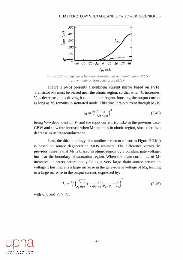
CHAPTER 2. LOW VOLTAGE AND LOW POWER TECHNIQUES
41
Figure 2.25. Comparison between conventional and nonlinear FVFCS
current mirror (extracted from [41])
Figure 2.24(b) presents a nonlinear current mirror based on FVFs.
Transistor M7 must be biased near the ohmic region, so that when Iin increases,
VDS7 decreases, thus driving it to the ohmic region, boosting the output current
as long as M8 remains in saturated mode. This time, drain current through M8 is:
𝐼8 =𝛽8
2(
𝐼𝑖𝑛
𝛽7𝑉𝐷𝑆7)
2
(2.45)
being VDS7 dependent on Vb and the input current Iin. Like in the previous case,
GBW and slew rate increase when M7 operates in ohmic region, since there is a
decrease in its transconductance.
Last, the third topology of a nonlinear current mirror in Figure 2.24(c)
is based on source degeneration MOS resistors. The difference versus the
previous cases is that M7 is biased in ohmic region by a constant gate voltage,
but near the boundary of saturation region. When the drain current Iin of M7
increases, it enters saturation, yielding a very large drain-source saturation
voltage. Thus, there is a large increase in the gate-source voltage of M8, leading
to a large increase in the output current, expressed by:
𝐼8 =𝛽8
2(√
2𝐼𝑖𝑛
𝛽10+
2𝐼𝑖𝑛
𝜆7𝛽7(𝑉𝑏−𝑉𝑇𝐻)2 −1
𝜆7)
2
(2.46)
with 0 and Vb > Vth.

CHAPTER 2. LOW VOLTAGE AND LOW POWER TECHNIQUES
42
2.3 Conclusions
This chapter summarizes some of the techniques employed in order not
only to obtain low voltage and low power circuits, but also to maximize the
performance of the blocks. Moreover, some applications have been presented,
making use of different techniques. Focus has been on QFGMOS transistors,
adaptive biasing techniques and LCMFB, which will be employed in this thesis.

CHAPTER 2. LOW VOLTAGE AND LOW POWER TECHNIQUES
43
Bibliography of the Chapter
[1] D. Kahng and S. M. Sze, “A floating-gate and its application to
memory devices”, The Bell System Technical Journal, vol. 46, no. 6,
pp. 1288-1295, 1967.
[2] L. A. Glasser, “A UV write-enabled PROM”, Chapel Hill Conference
on VLSI, pp. 61-65, 1985.
[3] D. A. Kerns, J. Tanner, M. Sivilotti and J. Luo, “CMOS UV-writable
nonvolatile analog storage”, in Proceedings of Advanced Research in
VLSI, pp. 245-261, 1991.
[4] M. Lenzlinger and E. H. Snow, “Fowler-Nordheim tunneling into
thermally grown SiO2”, Journal of Applied Physics, vol. 40, no. 1,
pp. 278-282, 1969.
[5] P. Hasler, “Foundations of learning in analog VLSI”, PhD.
Dissertation, California Institute of Technology, Pasadena (CA), 1997.
[6] P. Hasler, A. G. Andreou, C. Diorio, B. A. Minch and C. A. Mead,
“Impact ionization and hot-electron injection derived consistently from
Boltzmann transport”, VLSI Design, vol. 8, pp. 455-461, 1998.
[7] J. Ramirez-Angulo, C. A. Urquidi, R. González-Carvajal, A. Torralba
and A. Lopez-Martin, “A new family of very low-voltage analog
circuits based on quasi-floating-gate transistors”, IEEE Transactions
on Circuits and Systems II: Analog and Digital Signal Process, vol. 50,
no. 5, pp. 214-220, 2003.
[8] O. Naess, E. A. Olsen, Y. Berg and T. S. Lande, “A low voltage second
order biquad using pseudo floating gate transistors”, in Proceedings of
the IEEE International Symposium on Circuits and Systems,
pp. 125-128, 2003.
[9] J. Ramírez-Angulo, A. J. López-Martín, R. G. Carvajal and
F. M. Chavero, “Very low-voltage analog signal processing based on
quasi- floating gate transistors”, IEEE Journal of Solid-State Circuits,
vol. 39, no. 3, pp. 434-442, 2004.

CHAPTER 2. LOW VOLTAGE AND LOW POWER TECHNIQUES
44
[10] I. Seo and R. M. Fox, “Comparison of quasi-/pseudo-floating gate
techniques and low-voltage applications”, Analog Integrated Circuits
and Signal Processing, vol. 47, no. 2, pp. 183-192, 2006.
[11] A. J. Lopez-Martin, L. Acosta, C. Garcia-Alberdi, R. G. Carvajal and
J. Ramirez-Angulo, “Power-efficient analog design based on the class
AB super source follower”, International Journal of Circuit Theory
and Applications, vol. 40, no. 11, pp. 1143-1163, 2012.
[12] J. Ramirez-Angulo, R. G. Carvajal, J. A. Galan, and A. Lopez-Martin,
“A free but efficient low-voltage class-AB two-stage operational
amplifier”, IEEE Transactions on Circuits and Systems II: Express
Briefs, vol. 53, no. 7, pp. 568-571, 2006.
[13] M. B. Barron, “Low level currents in insulated gate field effect
transistors”, Solid-State Electronics, vol. 15, no. 3, pp. 293-302,
1972.
[14] R. R. Troutman and S. N. Chakravarti, “Subthreshold characteristics of
insulated-gate field-effect transistors”, IEEE Transactions on Circuit
Theory, vol. 20, no. 6, pp. 659-665, 1973.
[15] R. R. Troutman, “Subthreshold slope for insulated gate field-effect
transistors”, IEEE Transactions on Electron Devices, vol. 22, no. 11,
pp. 1049-1051, 1975.
[16] T. Masuhara, J. Etoh and M. Nagata, “A precise MOSFET model for
low-voltage circuits”, IEEE Transactions on Electron Devices, vol. 21,
no. 6, pp. 363-371, 1974.
[17] R. W. J. Barker, “Small-signal subthreshold model for IGFET's”,
Electronics Letters, vol. 12, no. 10, pp. 260-262, 1976.
[18] E. Vittoz and J. Fellrath, “New analog CMOS ICs based on weak
inversion operation”, in Proceedings of the European Solid-State
Circuits Conference, Toulouse, pp. 12-13, 1976.
[19] E. Vittoz and J. Fellrath, “CMOS analog integrated circuits based on
weak inversion operation”, IEEE Journal of Solid-State Circuits,
vol. 12, no. 3, pp. 224-231, 1977.
[20] C. C. Enz and E. A. Vittoz, “CMOS low-power analog circuit design”,

CHAPTER 2. LOW VOLTAGE AND LOW POWER TECHNIQUES
45
Designing Low Power Digital Systems, Emerging Technologies.
pp. 79-133, 1996.
[21] E. Vittoz, “Micropower techniques”, Design of VLSI Circuits for
Telecommunications and Signal Processing, Prentice Hall, 1991.
[22] C. Enz, F. Krummenacher and E. Vittoz, “An analytical MOS transistor
model valid in all regions of operation and dedicated to low-voltage
and low-current applications”, Analog Integrated Circuits and Signal
Processing, vol.8, no. 1, pp. 83-114, 1995.
[23] E. Vittoz, “Weak inversion in analog and digital circuits”, California
Co-op Conference Workshop, pp. 1-33, 2003.
[24] A. Wang, B. H. Calhoun and A. P. Chandrakasan, “Sub-threshold
design for ultra low-power systems”, Springer, 2006.
[25] P.W. Allen, B. J. Blalock and G. A. Rincon, “A 1V CMOS op-amp
using bulk-driven MOSFETs”, 41st IEEE International Solid-State
Circuits Conference ISSCC, pp 192-193, 1995.
[26] B. J. Blalock and P. E. Allen, “A low-voltage, bulk-driven MOSFET
current mirror for CMOS technology”, IEEE International Symposium
on Circuit and Systems, vol. 3, pp 1972-1975, 1995.
[27] J. Ramirez-Angulo, R. G. Carvajal, J. Tombs and A. Torralba, “Simple
technique for opamp continuous-time 1 V supply operation”,
Electronics Letters, vol. 35, no. 4, 1999.
[28] J. Ramirez-Angulo, A. Torralba, R. G. Carvajal and J. Tombs,
“Low-voltage CMOS operational amplifiers with wide input-output
swing based on a novel scheme”, IEEE Transactions on Circuits and
Systems I: Fundamental Theory and Application, vol. 47, no. 5,
pp. 772-774, 2000.
[29] S. Pourashraf, J. Ramirez-Angulo and A. Diaz-Sanchez, “Ultra low
voltage gate driven bandpass PGA with constant bandwidth”, IEEE
International Symposium on Circuits and Systems (ISCAS), 2018.
[30] X. Fan and P. K. Chan, “Analysis and design of low-distortion CMOS
source followers”, IEEE Transactions on Circuits and Systems I:
Regular Papers, vol. 52, no. 8, pp. 1489-1501, 2005.

CHAPTER 2. LOW VOLTAGE AND LOW POWER TECHNIQUES
46
[31] J. Ramirez-Angulo, R. G. Carvajal, A. Torralba, J. Galan,
A. P. Vega-Leal, and J. Tombs, “The Flipped Voltage Follower:
A useful cell for low- voltage low-power circuit”, Proceedings of IEEE
International Symposium on Circuits and Systems (ISCAS 02), vol. 3,
pp. 615-618, 2002.
[32] R. Gonzalez-Carvajal, J. Ramirez-Angulo, A. J. Lopez-Martin,
A. Torralba, J. A. Gomez Galan, A. Carlosena, and F. Muñoz Chavero,
“The flipped voltage follower: a useful cell for low-voltage low-power
circuit design”, IEEE Transactions on Circuits and Systems I: Regular
Papers, vol. 52, no. 7, pp. 1276-1291, 2005.
[33] M. G. Degrauwe, J. Rijmenants, E. A. Vittoz and H. J. De Man,
“Adaptive biasing CMOS amplifiers”, IEEE Journal of Solid-State
Circuits, vol. 17, no. 3, pp. 522-528, 1982.
[34] A. Lopez-Martin, S. Baswa, J. Ramirez-Angulo and
R. Gonzalez-Carvajal, “Low-voltage super class AB CMOS OTA cells
with high slew rate and power efficiency”, IEEE Journal of Solid-State
Circuits, vol. 40, no. 5, pp. 1068-1077, 2005.
[35] S. Baswa, A. J. Lopez-Martin, J. Ramirez-Angulo, and R. G. Carvajal,
“Low-voltage micropower super class AB CMOS OTA”, Electronics
Letters, vol. 40, pp. 216-217, Feb. 2004.
[36] V. Peluso, P. Vancorenland, M. Steyaert, and W. Sansen, “900 mV
differential class AB OTA for switched opamp applications”,
Electronics Letters, vol. 33, pp. 1455-1456, Aug. 1997.
[37] R. Castello and P. R. Gray, “A high-performance micropower
switched- capacitor filter”, IEEE Journal of Solid-State Circuits, vol.
SC-20, no. 6, pp. 1122-1132, Dec. 1985.
[38] S. Baswa, A. J. Lopez-Martin, R. G. Carvajal, and J. Ramirez-Angulo,
“Low-voltage power-efficient adaptive biasing for CMOS amplifiers
and buffers”, Electronics Letters, vol. 40, pp. 217-219, 2004.
[39] J. Ramirez-Angulo, R. Gonzalez-Carvajal, A. Torralba, and C. Nieva,
“A new class AB differential input stage for implementation of low
voltage high slew rate op-amps and linear transconductors”,
Proceedings of. International Symposium of Circuits and Systems,

CHAPTER 2. LOW VOLTAGE AND LOW POWER TECHNIQUES
47
pp. I 671-I 674, 2001.
[40] J. Ramirez-Angulo and M. Holmes, “Simple technique using local
CMFB to enhance slew rate and bandwidth of one-stage CMOS
op-amps”, Electronics Letters, vol. 38, no. 23, 2002.
[41] J. Galan, A. López-Martín, R. Gonzalez-Carvajal, J. Ramirez-Angulo
and C. Rubia-Marcos, “Super class-AB OTAs with adaptive biasing
and dynamic output current scaling”, IEEE Transactions on Circuits
and Systems I: Regular Papers, vol. 54, no. 3, 2007.

CHAPTER 2. LOW VOLTAGE AND LOW POWER TECHNIQUES
48

49
Chapter 3
SUBTHRESHOLD LOGIC FAMILY
A logic gate is an electronic device that implements a Boolean function.
Signals are represented as “0” or “1”, despite being electronic voltages. There
are different logic gates, depending on the Boolean function that they perform.
These gates are grouped into logic families, each one with its own distinctive
features. Nowadays, the most used logic family is the CMOS one, due to its very
low static consumption and adaptability to the dominant CMOS technologies.
However, conventional operation of CMOS transistors requires supply voltage
above their threshold voltage. In early 1970s, [1] made great advances based on
subthreshold operation. Since then, different analog subthreshold circuits were
developed for low-power applications [2], [3]. However, digital subthreshold
circuits did not receive the same interest until the late 1990s [4]-[6]. These
proposals often used body biasing, which is often not convenient, since the
severe reduction of the supply voltage causes a strong performance degradation:
the delay of the circuits increases exponentially and the leakage becomes very
relevant [7].
In this Chapter, a new subthreshold logic family is proposed, based on
QFG [8] transistors which were presented in the previous chapter, in order to
decrease the supply voltage. Setting the DC gate voltage of a QFG transistor to
a supply rail, the input capacitive coupling allows shifting this gate voltage
above the positive supply rail or below the negative supply rail. This way, the
pull-up or pull-down output transistors of a CMOS logic gate can be operated
even with supply voltages well below the threshold voltage VTH. Since
VDD<|VTH|, and due to the attenuation of such capacitive coupling, the peak

CHAPTER 3. SUBTHRESHOLD LOGIC FAMILY
50
voltage over (or below) the supply rail in the QFG gate is never larger than
0.5VTH, so the reverse p-n junction that isolates the drain and source terminals
from the bulk is not forward biased.
In particular, the design of four logic gates will be addressed in this
Chapter. Section 3.1 presents the QFG CMOS inverter. In Section 3.2, the QFG
MOS NAND, NOR and XOR logic gates are explained. Two applications of
these improved logic gates are included in Section 3.3: a ring oscillator and a
clock doubler. Finally, some conclusions are drawn in Section 3.4.
3.1 QFG CMOS Inverter
The schematic of the proposed QFG CMOS inverter is shown in
Figure 3.1. It employs a 1-input QFG pMOS transistor MP whose DC gate
voltage is set to VGMP,DC = VSS by the large resistance of a minimum-size
transistor MRlarge1 in cutoff region, and whose AC voltage VGMP,AC results from
the AC input voltage applied to the capacitive divider formed by CP and the
parasitic capacitance at the gate of MP, i.e., VGMP,AC = aPVIN,AC where
aP CP/(CP+CGS,MP). Since VIN is a square waveform swinging from VDD to VSS,
VIN,AC = ±VDD/2 (assuming VSS = 0 V), so when VIN = 0 V, VGMP,AC = -aPVDD/2
and VSG,MP = (1+aP/2)VDD. Choosing CP sufficiently larger than CGS,MP,
VSG,MP 1.5VDD and the pMOS transistor can provide a relatively large current
to the output node even with VDD<|VTH|. Similarly, the 1-input QFG nMOS
transistor MN has a DC voltage VGMN,DC = VDD set by the large resistance of a
transistor MRlarge2 in cutoff region, and AC voltage VGMN,AC = aNVIN,AC where
aN CN/(CN+CGS,MN). Choosing CN sufficiently larger than CGS,MN, when
VIN = VDD, VGS,MN 1.5VDD and the nMOS transistor is able to collect a relatively
large current from the output node.
The achievement of |VGS|>VDD in the output transistors allows operation
with VDD<|VTH| generating much larger output currents than when |VGS| is limited
to VDD and thus suffering from less speed degradation than conventional logic
operating in subthreshold region.

CHAPTER 3. SUBTHRESHOLD LOGIC FAMILY
51
Figure 3.1. NOT logic gate using QFG transistors
By using this improvement, the minimum supply voltage can be
reduced, in exchange of a larger die area. A 0.5 μm CMOS technology with
nominal NMOS and PMOS threshold voltages of 0.67 V and -0.96 V,
respectively, has been used to implement the whole family of logic gates. Note
the large threshold voltage values, which preclude very low voltage operation
using conventional CMOS logic.
The simulated Voltage Transfer Characteristics (VTC) of a standard
CMOS inverter in this technology for a supply voltage ranging from 0 to 2 V in
0.1 V steps are plot in Figure 3.2. Note that the inverter cannot operate properly
below 0.4 V. In the range from 0.4 V to about 0.9 V, despite the DC transfer
characteristics are correct, dynamic operation is limited since transistors operate
in weak inversion and deliver very low currents, leading to slow transients.
Figure 3.2. VTC of standard inverter

CHAPTER 3. SUBTHRESHOLD LOGIC FAMILY
52
Figure 3.3 shows the VTC of the QFG MOS inverter for VDD = 0.3 V,
showing the improvement achieved with the QFG transistors. The curve is
actually a transient simulation using a 10 Hz input ramp, since the QFG
capacitances have no effect in DC operation.
Figure 3.3. VTC of the QFG MOS inverter for VDD=0.3 V
A test chip prototype including the QFG MOS inverter was fabricated
and preliminary measurement results have been obtained. The coupling
capacitances employed have a value of 200 fF. A microphotograph of the
inverter is shown in Figure 3.4, enclosed in the white box. Silicon area employed
is approximately 900 m2.
Figure 3.4. Test chip microphotograph of the QFGMOS inverter
The experimental test setup employed is shown in Figure 3.5. The
Agilent 33522A signal generator is used to generate the input waveform, and
the unbuffered output is directly connected to the TDS 5104 oscilloscope using
a conventional test probe. Figure 3.6 shows the measured input and output

CHAPTER 3. SUBTHRESHOLD LOGIC FAMILY
53
signals of the inverter, showing proper operation at a supply voltage of 450 mV.
The circuit operates experimentally for supply voltages larger than
approximately 300mV, much less than the threshold voltage of the technology
employed. The maximum frequency of operation could not be tested due to the
direct connection of the inverter to the output, which represents a load
capacitance of about 30 pF including bonding pad, pin, board and probe
capacitances.
Figure 3.5. Measurement setup employed
Figure 3.6. Measured input and output voltage of the QFG MOS inverter
3.2 QFG NAND, NOR and XOR gates
The procedure described above can be easily applied to other logic
gates by just replacing each MOS transistor in the conventional CMOS gate by
the corresponding QFG MOS version. Thus, a complete QFG MOS logic family
can be generated. Figure 3.7 (a), (b) and (c) show for illustrative purposes a QFG
NAND, NOR and XOR gate, respectively, obtained following this procedure.

CHAPTER 3. SUBTHRESHOLD LOGIC FAMILY
54
(a) (b)
(c)
Figure 3.7. QFG Gates (a) NAND (b) NOR (c) XOR
These QFG MOS logic gates were verified only in simulation, showing
also proper operation at subthreshold supply voltages.

CHAPTER 3. SUBTHRESHOLD LOGIC FAMILY
55
3.3 Applications of logic gates
3.3.1 Ring Oscillator
The ring oscillator is a block that is formed by an odd number of NOT
logic gates connected in series. The last inverter is connected to the input of the
first NOT gate, creating a ring, hence its name. Due to the odd number of gates,
there is an instability that goes from one node to the next, generating an
oscillating signal in each of the nodes with different phase. Thus, it only needs
a constant supply voltage VDD to operate.
To evaluate the dynamic operation of the QFG MOS inverter,
an 11-stage ring oscillator was designed. The topology is shown in Figure 3.8.
Figure 3.8. Schematic of a ring oscillator
Figure 3.9 shows the simulated voltages at the gate of the pMOS (VGP)
and nMOS (VGN) output transistors of one of the QFG inverters of the oscillator
operating with VDD = 0.3 V. Note the DC level shifting of about ±VDD/2
theoretically predicted in the previous paragraphs.
Figure 3.9. Voltage at the gates of the QFG transistors, VDD=0.3V

CHAPTER 3. SUBTHRESHOLD LOGIC FAMILY
56
The oscillation frequency of the oscillator versus VDD is shown in
Figure 3.10. The result for the oscillator implemented with the conventional
CMOS inverter and a Floating Gate MOS (FGMOS) inverter [9] are also in the
same figure. Note that the conventional inverter cannot operate properly below
0.4 V and that the resulting oscillation frequencies are much lower than for the
QFG MOS inverter for the same VDD. This is because for a given VDD, the
transistors in the conventional inverter deliver much less transient current than
for the QFG MOS inverter due to their lower |VGS| voltage. The FGMOS version
allows even lower VDD. However, it requires complex circuits to program and
refresh the charge at the floating gates, and leads to increased static power
consumption.
Figure 3.10. Oscillation frequency vs VDD
3.3.2 Clock doubler
Clock signals are required to make synchronous logic circuits and
discrete-time circuits operate. In some cases, it is convenient to use clocks whose
amplitude is bigger than the supply voltage, since they are connected to the gate
of transistors which behave as switches. If the amplitude of the clock is not high
enough, the switches do not operate correctly, as they remain partially open or
closed. To avoid this situation, boosted clocks are employed, which can be
generated by a clock doubler.

CHAPTER 3. SUBTHRESHOLD LOGIC FAMILY
57
Figure 3.11. Implementation of a clock doubler
The implementation of the clock doubler can be seen in Figure 3.11
[10]. If the input clock Clk is VDD, inverter 2 forces 𝐶𝑙𝑘𝐵𝑜𝑜𝑠𝑡𝑒𝑑 to be VSS. The
capacitor C2 is charged through M2 until it reaches a value of VDD, whereas C1
was previously charged also to VDD. This makes VDD1 to be 2VDD, and as the
input of inverter 1 is VSS, the ClkBoosted is also 2VDD. On the contrary, when the
input clock is low, VDD2 is 2VDD, thus 𝐶𝑙𝑘𝐵𝑜𝑜𝑠𝑡𝑒𝑑 is 2VDD. At the same time,
ClkBoosted is VSS because of the inverter 1.
The conventional clock doubler of Figure 3.11 can be improved by
replacing the inverters by their QFG version, as shown in Figure 3.1. The
behavior of this enhanced clock doubler is the same as the conventional one.
However, due to the more convenient DC operating point, it can operate with
lower supply voltage. Besides, since the output currents of the QFG inverters
are greater, the clock doubler works faster.
The two versions of the clock doubler have been simulated in a 0.5 μm
n-well CMOS technology. For both circuits, M1 and M2 have an aspect ratio of
18 μm/600 nm, 30 pF capacitors have been used as C1 and C2, and inverters are
formed by a 18 μm/600 nm PMOS transistor and a 6 μm/600 nm NMOS
transistor. In the case of QFG logic gates, CBAT = 1 pF and the size of transistors
MRlarge is 1.5 μm/600nm. Negative supply voltage is connected to ground in both
cases, and as for the positive supply voltage, 0.7 V and 0.5 V has been used for
both the conventional and QFG circuit, respectively. The input clock has a

CHAPTER 3. SUBTHRESHOLD LOGIC FAMILY
58
frequency of 1 kHz, and the positive level is the same as the respective positive
supply voltage. Figure 3.12 (a) and (b) present the output boosted clocks. Note
that the theoretical value of the output (2VDD) is not achieved, as there is a small
voltage drop, which can be caused by the imperfect charge and discharge of the
capacitors C1 and C2, since this process is clock-sensitive.
(a) (b)
Figure 3.12. Boosted clocks obtained with (a) conventional clock doubler
(b) QFG clock doubler
3.4 Conclusions
Chapter 3 presents a subthreshold CMOS logic gate family. The use of
QFG MOS transistors lead to a reduction in the supply voltage, below its
threshold voltage. In addition, two possible applications of these improved logic
gates have been addressed.

CHAPTER 3. SUBTHRESHOLD LOGIC FAMILY
59
Bibliography of the Chapter
[1] R. M. Swanson and J. D. Meindl, “Ion-implanted complementary MOS
transistors in low-voltage circuits”, IEEE Journal of Solid-State
Circuits, vol. 7, no. 2, pp.146-153, 1972.
[2] E. Vittoz and J. Fellrath, “CMOS analog integrated circuits based on
weak inversion operation”, IEEE Journal of Solid-State Circuits,
vol. 12, no. 3, pp. 224-231, 1977.
[3] C. Mead, “Analog VLSI and neural systems”, Addison-Wesley, 1989.
[4] H. Soeleman and K. Roy, “Ultra low power digital subthreshold logic
circuits”, Proceedings of International Symposium on Low Power
Electronics and Design (ISLPED), pp. 94-96, ACM, 1999.
[5] B. C. Paul, H. Soeleman, and K. Roy, “An 8x8 sub-threshold digital
CMOS carry save array multiplier”, Proceedings of European Solid-
State Circuits Conference (ESSCIRC), pp. 377-380, 2001.
[6] M.J. Deen, M.H. Kazemeini and S. Naseh, “Performance
characteristics of an ultra-low power VCO”, Proceedings of
International Symposium on Circuits and Systems (ISCAS),
pp. 697-700, 2003.
[7] B. Zhai, D. Blaauw, D. Sylvester and K. Flautner, “Theoretical and
practical limits of dynamic voltage scaling”, ACM/IEEE Design
Automation Conference (DAC), pp. 868-873, 2004.
[8] J. Ramirez-Angulo, A.J. Lopez-Martin, R.G. Carvajal and
F. Munoz- Chavero, “Very low voltage analog signal processing based
on quasi floating gate transistors”, IEEE Journal of Solid-State
Circuits, vol. 39, no. 3, pp 434-442, 2003.
[9] E. Mendez-Delgado and G.J. Serrano, “A 300mV low-voltage start-up
circuit for energy harvesting systems”, Proceedings of International
Symposium on Circuits and Systems (ISCAS), pp. 829-832, 2011.

CHAPTER 3. SUBTHRESHOLD LOGIC FAMILY
60
[10] Y. Nakagome, H. Tanaka, K. Takeuchi, E. Kume, Y. Watanabe,
T. Kaga, Y. Kawamoto, F. Murai, R. Izawa, D. Hisamoto, T. Kisu,
T. Nishida, E. Takeda and K. Itoh, “An experimental 1.5-V 64-Mb
DRAM”, IEEE Journal of Solid-State Circuits, vol. 26, no. 4,
pp. 465-472, 1991.

61
Chapter 4
SINGLE-ENDED CLASS AB
AMPLIFIERS
As mentioned in previous chapters, amplifiers are one of the most
widely used analog building blocks, as they are required in almost every
application. Most integrated amplifiers have a differential input. To realize this
differential input, almost all amplifiers use what is commonly called a
differential transistor pair.
If the output current is controlled by the differential input voltage, the
amplifier is known as Operational Transconductance Amplifier, or OTA, being
Gm = Iout / Vid the transconductance gain. It can be said that OTAs are voltage
controlled current sources (VCCS) with high gain.
A common method in order to increase the gain of the amplifier is using
a cascode configuration, since its output resistance is higher than that of the
conventional scheme. The main cascode topologies to design OTAs are depicted
in Figure 4.1: (a) symmetric or current mirror OTA, (b) telescopic, (c) folded
cascode and (d) recycling folded cascode. However, the symmetric topology is
not going to be treated in this chapter, since many optimization efforts have
already been made [1], [2]. By applying the techniques explained in Chapter 2,
these different topologies are modified in this Chapter, obtaining improved
performance.

CHAPTER 4. SINGLE-ENDED CLASS AB AMPLIFIERS
62
Figure 4.1. Cascode Topologies (a) Symmetric amplifier (b) Telescopic
(c) Folded Cascode (d) Recycling Folded Cascode

CHAPTER 4. SINGLE-ENDED CLASS AB AMPLIFIERS
63
Structure of Chapter 4 is as follows. Section 4.1 is divided in three
sections, each one explaining how improved versions of the different OTA
topologies can be obtained. First, an enhanced telescopic cascode OTA is
proposed in Section 4.1.1. Section 4.1.2 includes a modified folded cascode
OTA, and finally, several enhanced recycling folded cascode OTAs are shown
in Section 4.1.3. In order to collect the main characteristics of the amplifiers
proposed in Section 4.1, a table is presented in Section 4.2, including other class
AB amplifiers, with the aim of comparing them. Finally, some conclusions are
drawn in Section 4.3.
4.1 OTA Topologies
In this Section, several proposed OTAs are presented. They can be
classified in 3 subsections, depending on which type of OTA topology they are
based.
4.1.1 Telescopic Cascode
Telescopic cascode op-amps (Figure 4.2(b)) are popular since they
usually provide the best trade-off between gain, power dissipation, speed, and
noise. They also present optimal current efficiency CE = Iout/Isupply, being this
parameter the ratio between the output current Iout to the total supply current
Isupply. In order to obtain an optimal CE, a single branch from the supply rails to
the output terminal is required, thus avoiding to waste current by extra branches
replicating internally the signal currents. However, this means that input
transistors must be in the output branch and therefore the input common-mode
range and output swing are reduced. To mitigate these negative effects, cascode
self-biasing schemes have been proposed that implement a floating battery
between the common source of M1-M2 and the common gate of M1C-M2C [3].
This way, variations in the common-mode input voltage are sensed at the
common source node VS and conveyed to the gate of M1C-M2C, allowing low VDS
values for M1-M2 to improve output swing without degrading input common-
mode range. However, such floating battery has been often implemented by a
diode-connected transistor (or less frequently by a resistor) biased by two
matched DC current sources, which increases static power consumption and
matching requirements.

CHAPTER 4. SINGLE-ENDED CLASS AB AMPLIFIERS
64
Figure 4.2. Telescopic OTAs (a) Conventional (b) Class AB
(c) Proposed QFG Class AB
Another drawback of the opamp of Figure 4.2(a) is that it operates in
class A, delivering a maximum output current limited by the bias current. Hence
a trade-off between static power dissipation and dynamic performance exists.
An adaptive bias current source can be used instead to get class AB operation.
However, in this case although self-biasing was used in the PMOS cascode
transistors, the large dynamic currents generated can make transistors M3-M4

CHAPTER 4. SINGLE-ENDED CLASS AB AMPLIFIERS
65
leave saturation, reducing slew rate (SR). Hence dynamic biasing is also
required for the NMOS cascode transistors.
A class AB single-stage telescopic cascode opamp is proposed. It
employs an adaptive bias current source and a dynamic biasing technique for
the cascode transistors which does not lead to extra power consumption or
matching requirements.
Figure 4.2(b) shows the telescopic cascode opamp with the adaptive
bias circuit employed. Transistors M5, M6, M7 and M8 and bias current sources
IBIAS implement a maximum circuit [4] that sets voltage VS = max(VIN+, VIN-)+VB,
where DC voltage VB is the quiescent VSG voltage of M7-M8. In quiescent
operation VSG1,2=VB, so quiescent current in M1-M2 is accurately set to IBIAS/n
with n = (W/L)7,8 / (W/L)1,2 regardless of process, supply voltage or temperature
variations. When VIN- < VIN+, M7 enters triode region and VS is set to VIN+ + VB,
so VSG1 = VB + VIN+ - VIN-, i.e., M1 experiences the full input signal swing and a
large dynamic current not bounded by IBIAS is generated at M1. Analogously,
when VIN- > VIN+ then VS = VIN+ + VB and a large dynamic current is created in
M2. However, in small signal operation the common source node is a
small-signal ground, so AC small signal currents in M1-M2 are like in
Figure 4.2(a) and gain-bandwidth product (GBW) is not improved by the
adaptive biasing.
Despite the large dynamic current that can potentially be generated, the
circuit of Figure 4.2(b) is not efficient since the static biasing at the cascode
transistors can make M1 and/or M3-M4 enter triode region for VIN- < VIN+ or can
turn M2 in triode mode for VIN- > VIN+. To solve it, cascode transistors are
dynamically biased using Quasi-Floating Gate (QFG) techniques [5] as shown
in Figure 4.2(c). As described in Section 2.1.2, minimum-size transistors MR1
and MR2 are pseudo resistors with very large resistance Rlarge. Hence capacitors
CBAT cannot discharge rapidly and behave as floating DC level shifters,
transferring signal variations from the common source of M1-M2 to the gate of
M1C-M2C and from the gate of M3-M4 to the gate of M3C-M4C. In quiescent state
capacitors CBAT are open circuits and the op-amp is equivalent to Figure 4.2(b).
However, in dynamic operation the cascode biasing allows handling large signal
currents. Note that no extra power consumption or matching requirements are
needed for the dynamic biasing employed. Moreover, due to the extremely large
Rlarge values achieved, CBAT < 1 pF can be employed, reducing the silicon area
overhead.

CHAPTER 4. SINGLE-ENDED CLASS AB AMPLIFIERS
66
Concerning small signal operation, the DC gain Ad and GBW of the
three opamps of Figure 4.2 are the same:
Ad = gm1,2·Rout ≈ gm1,2·(gm2c·ro2c·ro2 || gm4c·ro4c·ro4) (4.1)
GBW = gm1,2/(2πCL) (4.2)
with gmi and roi are the transconductance and output resistance, respectively, of
transistor Mi. However, CMRR is improved in Figure 4.2(c) as the dynamic
cascode biasing tracks input common-mode variations from the common source
node VS to the gate of M1C-M2C, keeping the VDS of M1-M2 almost constant.
A test chip prototype with the amplifiers of Figure 4.2 was fabricated
in a 0.5 μm CMOS process. Poly-poly capacitors CBAT were used with a nominal
value of 850 fF. Transistor aspect ratios are shown in Table 4.1. A
microphotograph of the three amplifiers is shown in Figure 4.3, where their
relative areas can be assessed.
Transistor W/L (μm/μm)
M1, M2 100/1.05
M3, M4 120/0.6
M1C, M2C, M3, M4 200/0.6
M5, M5B, M6 100/0.6
M7, M8 100/1.05
MR1, MR2 1.5/1.05
Table 4.1. Transistors aspect ratios of telescopic OTA in Figure 4.2
Figure 4.3. Microphotograph of the three telescopic OTAs

CHAPTER 4. SINGLE-ENDED CLASS AB AMPLIFIERS
67
Measurements were done using the amplifiers in unity-gain negative
feedback as voltage followers. Supply voltage was ±1 V. No external load
capacitance was used, so CL corresponds to the capacitance of the test setup (pad,
board and test probe) and is approximately 20 pF. The measured transient
response of the three amplifiers is shown in Figure 4.4. The class A amplifier
corresponds to Figure 4.2(a), Class AB to Figure 4.2(b) and the proposed one to
Figure 4.2(c). A 100 kHz 1 V input square wave was used. Note the improved
SR and output swing achieved with the circuit of Figure 4.2(c).
Figure 4.4. Measured transient response of the circuits of Figure 4.2
Figure 4.5. Measured magnitude response of the Acm of circuits of Figure 4.2

CHAPTER 4. SINGLE-ENDED CLASS AB AMPLIFIERS
68
The measured magnitude response of the common-mode gain
Acm=vout/vicm is shown in Figure 4.5. Higher Acm (hence lower CMRR=Ad/Acm)
in Figure 4.2(b) vs Figure 4.2(a) is due to the smaller output resistance of the
adaptively biased current source M5-M8 vs the current source M5B in
Figure 4.2(a). However, the dynamic cascode biasing in Figure 4.2(c) improves
noticeably Acm and hence CMRR, as mentioned above.
Table 4.2 summarizes the main performance parameters of the opamps
of Figure 4.2. The measured THD for Figure 4.2(c) is higher due to the improved
signal swing and SR achieved. A comparison with other micropower class AB
amplifiers is shown in Figure 4.6, using the figure of merit
FoM = SR·CL/Isupply = ImaxL/Isupply, where Isupply is the total static current
consumption. Note the improved FoM vs power data achieved for the proposed
opamp of Figure 4.2(c).
Parameter Figure 4.2(a) Figure 4.2(b) Figure 4.2(c)
Slew Rate 1 V/μs 5.3 V/μs 8.9 V/μs
THD @100kHz,
0.7Vpp -18.1 dB -14.1 dB -41.9 dB
DC gain (*) 54.1 dB 54.6 dB 54.6 dB
PM (*) 88.7º 88.4º 88.4º
GBW (*) 1.15 MHz 1.15 MHz 1.15 MHz
CMRR 55.3 dB 53.2 dB 62.4 dB
PSRR+ 85.1 dB 73.6 dB 77.6 dB
PSRR- 68.9 dB 65.8dB 67.3 dB
Eq. input noise
@1MHz (*) 22 nV/√Hz 23 nV/√Hz 23 nV/√Hz
Power 80 μW 80 μW 80 μW
Area 0.019 mm2 0.020 mm2 0.023 mm2
(*)Simulation
Table 4.2. Measured performance summary and comparison between op-amps
of Figure 4.2 (CL = 20 pF)

CHAPTER 4. SINGLE-ENDED CLASS AB AMPLIFIERS
69
Figure 4.6. Performance comparison between other op-amps
To sum up this section, a micropower telescopic opamp has been
proposed. It employs various adaptive biasing techniques for providing bias
currents and cascode bias voltages. These techniques improve dynamic
operation maintaining supply voltage requirements and quiescent currents,
without degrading other performance metrics.
4.1.2 Folded Cascode
As it was mentioned in Chapter 2, class AB amplifiers are widely used
in applications requiring low power consumption due to their capacity to yield
large dynamic currents not limited by the quiescent currents. Thus, low static
power consumption can be obtained without degrading dynamic performance.
An adaptive bias circuit for the differential pair is usually employed to get the
required current boosting, providing very low quiescent currents in order to have
very low static power dissipation. However, when a large differential input
signal is applied, these adaptive bias circuits are able to provide large dynamic
currents, with maximum swings larger than the quiescent current level.

CHAPTER 4. SINGLE-ENDED CLASS AB AMPLIFIERS
70
Figure 4.7. Folded Cascode (a) Conventional Class A OTA
(b) Proposed Class AB OTA
Several proposals have been reported to provide class AB operation to
classic amplifier topologies like telescopic and current mirror OTAs, e.g. [1],
[6], [11]. However, achieving class AB operation in a folded cascode amplifier
(Figure 4.7(a)) is more complex. Adaptive biasing of the input pair is not
effective by itself in this case since the bottom current sources limit the
maximum output current. As these current sources force the sum of currents
through M1 and M5 to be 2IBIAS, and the same with the sum of currents through
M2 and M6, the maximum output current is 2IBIAS regardless of the adaptive
biasing circuit used for the input pair. Therefore, it is mandatory that these bias

CHAPTER 4. SINGLE-ENDED CLASS AB AMPLIFIERS
71
current sources also adapt to the input signal to achieve power efficiency. Thus,
multi-path schemes [12], [13] or current recycling techniques [14]-[17] are
usually employed to enhance the performance of the folded cascode amplifier,
replacing these current sources by active current mirrors. However, the power
efficiency achieved with these techniques is limited since the active current
mirrors lead to internal replication of large dynamic currents at the additional
branches [1]. A simple modification of the conventional folded cascode OTA is
proposed which enhances the performance of the amplifier without this
drawback.
Figure 4.7 (a) and (b) shows the conventional class A folded cascode
OTA and the proposed class AB OTA, respectively. The constant differential
pair bias source 2IB of Figure 4.7(a) is replaced in Figure 4.7(b) by an adaptive
circuit to bias M1 and M2. Besides, the current sources 2IB at the folding stage
of conventional OTA are replaced by another adaptive biasing circuit in the
proposed OTA, so that the limitation in output current is avoided.
In order to implement the adaptive biasing circuit of the input pair,
cross-coupled floating batteries are used (previously explained in
Section 2.2.3.1) [1],[18]. The employed topology is shown in Figure 2.20. This
way, thanks to two Flipped Voltage Followers (FVFs) [19], in quiescent
conditions, accurate low quiescent currents are provided and in dynamic
conditions, large currents are achieved, not bounded by 2IB. In addition, the full
differential input signal is applied to each differential pair transistor, thus
doubling DC gain compared to class A OTA.
However, although the adaptive biasing circuit of the input stage would
double DC gain (and GBW), it could not increase dynamic output currents, as
currents in the output branches are limited by the current sources of the folding
stage. To overcome this issue, here current sources are also adaptively biased,
this time by using Quasi-Floating Gate transistors [20], [21]. The concept of
using QFGMOS transistors to achieve class AB operation was previously
described in Section 2.1.2 (see Figure 2.6). Thus, an efficient implementation of
a DC level shifter is obtained only with a capacitor and a high value resistance.
The quiescent current through M3 and M4 is still 2IB but under dynamic
conditions, voltages at the gates of M3 and M4 experience a swing dependent on
VIN, creating an extra signal path.

CHAPTER 4. SINGLE-ENDED CLASS AB AMPLIFIERS
72
The schematic of the proposed Class AB folded cascode OTA is shown
in Figure 4.8. Note that the QFG transistors M3 and M4 are not directly
connected to the input signal. They re-use the FVFs to invert and scale the input
signals to fit the signal swing at the gates of M3 and M4 and to avoid extra
loading of the input terminals by the adaptive biasing of the folding stage.
Figure 4.8. Proposed class AB folded cascode OTA
In quiescent operation, the proposed circuit works like the conventional
OTA in Figure 4.7(a), with well controlled quiescent currents, as there is no
current flowing through the pseudo resistors MR1 and MR2. For large positive
differential input voltages, VID = VIN+ - VIN-, the gate voltage of M2B decreases
and that of M2A increases. As it was mentioned in Chapter 2, capacitors CBAT act
as floating batteries that decrease the gate voltage of M4 and increase that of M3.
Thus, a large output current is sourced to the load, yielding large positive Slew
Rate SR+. For negative VID, something similar happens. The gate voltage of M2B
increases and that of M2A decreases, increasing the gate voltage of M4 and
decreasing that of M3, leading to a large output current sunk from the load that
boosts SR-.
If small-signal analysis is considered, the adaptive biasing employed in
Figure 4.8 not only increases slew rate, it also significantly increases the
transconductance Gm of the conventional OTA for the same bias current and
transistor sizes. The transconductance of the conventional folded cascade OTA
is defined by:

CHAPTER 4. SINGLE-ENDED CLASS AB AMPLIFIERS
73
𝐺𝑚𝐴 = 𝑔𝑚1 = 𝑔𝑚2 (4.3)
while that of the proposed OTA in Figure 4.8 is:
𝐺𝑚𝐴𝐵 = 2𝑔𝑚1 (1 + 𝛼𝑔𝑚3,4
𝑔𝑚2𝐴,2𝐵) (4.4)
with CBAT/(CBAT + Cgs3,4). Thus, the increase factor is 2·(1+·gm3,4/gm2A,2B).
The factor 2 is caused by the adaptive biasing circuit of the differential pair and
the term 1+·gm3,4/gm2A,2B corresponds to the adaptive current sources M3 and
M4. The same enhancement factor is present in the GBW of the proposed class
AB OTA compared to the conventional class A OTA. The DC gain of the class
AB OTA is also increased, but to a less extent since the output resistance Rout of
the class AB OTA is also slightly decreased due to the nonzero output resistance
of the FVFs.
Figure 4.9. Simplified pole-zero diagram (not to scale)
Just like the conventional folded cascade OTA, the proposed OTA
features a dominant pole p1 = -1/(Rout·Cout) set by the output terminal as well
as a non-dominant pole p3 -gm5,6/Cp5,6 corresponding to the source terminals
of M5 and M6. In these expressions Cout CL is the output capacitance and Cp5,6
is the parasitic capacitance at the source of M5 and M6, which corresponds to
Cgs5,6 plus other smaller capacitances. In addition, the circuit in Figure 4.8 has
an additional non-dominant pole p2 -gm2A,2B/(CA + ·CB), due to the extra
signal path introduced, where CA and CB are the parasitic capacitances at nodes
A and B, respectively. CA is approximately Cgs2A,2B plus the bottom plate to the
substrate parasitic capacitance of CBAT, and CB is approximately Cgs3,4 plus the
top plate to substrate parasitic capacitance of CBAT. All these poles are depicted
in Figure 4.9, where it is assumed that non-dominant poles are beyond the
unity-gain frequency u. Since p2 is associated to PMOS devices, and
CA + ·CB is generally larger than Cp3,4, p2 is at lower frequencies than p3.
Hence p2 yields a reduction in phase margin compared to the class A version.

CHAPTER 4. SINGLE-ENDED CLASS AB AMPLIFIERS
74
For this additional pole frequency to be at least 3 times the GBW, the required
CL is approximately
𝐶𝐿 > 6𝑔𝑚1,2
𝑔𝑚2𝐴,2𝐵(1 + 𝛼
𝑔𝑚3,4
𝑔𝑚2𝐴,2𝐵) · (𝐶𝐴 + 𝛼𝐶𝐵) (4.5)
As for the slew rate, that of the conventional folded cascode in
Figure 4.7(a) is
𝑆𝑅𝐴+ = 𝑆𝑅𝐴− =2𝐼𝐵
𝐶𝐿 (4.6)
since 2IB is the maximum current sourced to the load of sunk from it. Thus,
symmetrical positive and negative slew is provided but the maximum output
current is limited by the bias current. In the case of proposed folded cascode
OTA, the expression for the slew rate is
𝑆𝑅𝐴𝐵+ = 𝑆𝑅𝐴𝐵− =2𝐼𝐵
𝐶𝐿(1 + 𝛼√
𝛽3,4
𝛽2𝐴,2𝐵) (4.7)
with i = ·Cox(W/L)i, evidencing the SR improvement achieved.
Both the class A and class AB folded cascode OTA circuits of
Figure 4.7(a) and Figure 4.8 were fabricated in a 0.5 m CMOS test chip
prototype. A microphotograph of that chip is shown in Figure 4.10, where the
OTAs are enclosed by white rectangles. The transistor sizes employed are
included in Table 4.3. Poly-poly capacitors CBAT were used, with a value of
0.7 pF. Supply voltages where 1 V, and the bias current IB was 10 A. Cascode
bias voltages VCP and VCN were set to -0.2 V and 0 V, respectively. An external
load capacitor of 47 pF was used. The output was connected directly to a
bonding pad and no external buffer was employed. Thus, if the pad, board and
test probe capacitances are considered, the total load capacitance is increased to
approximately 70 pF.
Figure 4.10. Test chip microphotograph

CHAPTER 4. SINGLE-ENDED CLASS AB AMPLIFIERS
75
Transistor W/L (μm/μm)
M1-M2, M1A-M1B 100/1.5
M2A-M2B 9/0.6
M3-M4 120/0.6
M5-M8 200/0.6
M9-M10 200/1.05
M11 60/0.6
M12 100/0.6
MR1-MR2 1.5/0.6
Table 4.3. Transistor aspect ratio of class AB folded cascode OTA
The transient response of both fabricated OTAs was measured in unity
gain configuration, using a 1 MHz 0.5 V square wave with DC level of -0.6 V
at the input. The measured output of both OTAs are drawn in Figure 4.11. Note
the stable and faster settling of the proposed class AB OTA of Figure 4.8. The
SR+ for the class A OTA is 0.32 V/s and that of the proposed class AB OTA is
9.8 V/s, i.e., an increase factor of 30.6 for the same quiescent current and load
capacitance. The expected increase factor from Equation 4.7, with estimated
0.8, was 36.
Figure 4.11. Measured response of class A and class AB folded cascode OTAs

CHAPTER 4. SINGLE-ENDED CLASS AB AMPLIFIERS
76
As can be noticed from Equation 4.5, the OTA is suitable for relatively
large CL. To solve this limitation, lead compensation at the output terminal is
proposed, as shown in Figure 4.12. By using this method, lower CL values can
be employed.
Figure 4.12. Simplified AC model (a) Purely capacitive load
(b) with lead compensation
To analyze the effect of the added resistor RC, the basic single-pole AC
model of the FC OTA will be used for simplicity. The transfer function of
Figure 4.12(a) is
𝐻(𝑠) =𝑉𝑜𝑢𝑡(𝑠)
𝑉𝑖𝑛(𝑠)=
𝐺𝑚𝑅𝑜𝑢𝑡
1+𝑠𝑅𝑜𝑢𝑡𝐶𝐿 (4.8)
If a resistor RC is placed in series with the capacitive load, as
Figure 4.12(b) shows, the transfer function becomes
𝐻(𝑠) =𝑉𝑜𝑢𝑡(𝑠)
𝑉𝑖𝑛(𝑠)=
𝐺𝑚𝑅𝑜𝑢𝑡(1+𝑠𝑅𝐶𝐶𝐿)
1+𝑠(𝑅𝑜𝑢𝑡+𝑅𝐶)𝐶𝐿 (4.9)
Thus, the lead compensation resistance RC creates a zero
ωz ≈ -1/(RC·CL) that can be placed at different locations to improve phase margin
and settling performance [22]. The strategy followed here is to choose RC in
order to make ωz slightly larger than the unity-gain frequency, leading to a phase
lead equal to arctan(ωz/GBW) rads in the phase margin. In addition, it can be
deduced from expression 4.9 that the output pole is modified by RC, but if
RC << Rout, this variation can be neglected.
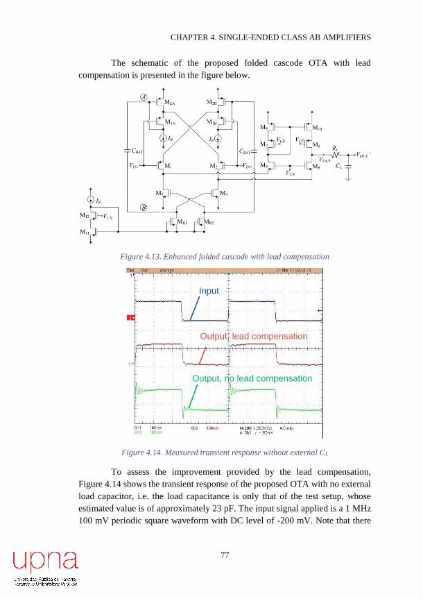
CHAPTER 4. SINGLE-ENDED CLASS AB AMPLIFIERS
77
The schematic of the proposed folded cascode OTA with lead
compensation is presented in the figure below.
Figure 4.13. Enhanced folded cascode with lead compensation
Input
Output, lead compensation
Output, no lead compensation
Figure 4.14. Measured transient response without external CL
To assess the improvement provided by the lead compensation,
Figure 4.14 shows the transient response of the proposed OTA with no external
load capacitor, i.e. the load capacitance is only that of the test setup, whose
estimated value is of approximately 23 pF. The input signal applied is a 1 MHz
100 mV periodic square waveform with DC level of -200 mV. Note that there

CHAPTER 4. SINGLE-ENDED CLASS AB AMPLIFIERS
78
is a significant ringing in the output waveform when no lead compensation is
employed, which degrades settling performance. The inclusion of a lead
resistance Rc of 772 Ω improves settling performance significantly, as the red
curve shows.
The measured magnitude response of the class A and class AB OTAs
as voltage followers is shown in Figure 4.15. The cutoff frequency of the
proposed OTA is 4.75 MHz, while that of the conventional OTA is 310 kHz.
Due to the dominant pole design, these frequencies correspond approximately
to the GBW of the OTAs. Thus, the experimental increase factor in GBW is
15.3. The expected value from Equation 4.4 with 0.8 was 12.2.
Figure 4.15. Measured closed-loop magnitude response of conventional class A OTA
(dashed line) and proposed class AB OTA (solid line)
Table 4.8 sums up the main measurement results for both OTAs. Note
that the settling time in the proposed OTA is lower than 100 ns, whereas the
conventional OTA is unable to settle for this input signal and load. Measured
Total Harmonic Distortion (THD) is <1% for a 1 Vpp input sinusoidal signal,
while the conventional OTA presents a THD >6% due to settling limitations.
The open-loop frequency response could not be measured because of the high
gain. Simulation results for DC gain and phase margin are provided instead. The
increase in DC gain of the proposed OTA is 14.6 dB (i.e. a factor of 5.37), lower
than the GBW increase factor due to the reduced output resistance. These results
agree with theoretical analysis. The main disadvantage of the proposed OTA is

CHAPTER 4. SINGLE-ENDED CLASS AB AMPLIFIERS
79
the decrease in phase margin. The PM of the conventional OTA drops to 79º at
4.75 MHz, so the proposed OTA shows a degradation of 19º.
The proposed OTA presents a slightly lower equivalent input noise
level, due to the increased gain. However, there is a 50% increase in the static
power because of the bias current required for the FVFs. Besides, silicon area is
a 20% higher due to capacitors CBAT. If the width of M1A and M1B is reduced by
a factor n than that of M1 and M2, the bias current of the FVF is also scaled by
n, and the extra required power would be 50/n %.
A performance comparison with other proposed class AB amplifiers is
also included in Table 4.8. To ease comparison, two conventional Figures of
Merit (FoM) are considered: FoML = SR·CL/Isupply=ImaxL/Isupply, where Isupply is the
total current consumption, which shows the large-signal current efficiency, and
FoMS=100·GBW·CL/Isupply (MHz·pF/μA) a small-signal speed/power ratio.
Note that the proposed OTA compares favorably for both FoMs.
As a conclusion, a class AB folded cascode OTA has been presented,
based on two adaptive biasing circuits for the differential input pair and the
folding stage. The use of FVFs and QFG transistors leads to a simple and
compact implementation and does not require extra supply voltage.
Measurement results show a significant increase in slew rate and fast settling,
maintaining low noise and low static power consumption. The circuit can find
application in low voltage low power switched capacitor circuits and in buffers
requiring to drive large capacitive load.
4.1.3 Recycling Folded Cascode
In the previous section, an improved version of the conventional folded
cascode OTA was discussed. Although its transconductance was improved
thanks to the use of QFG transistors at the folding stage, dynamic performance
can be further improved.
A highly power-efficient approach to achieve class AB amplifiers was
proposed in [1]. Although it employs the same adaptive biasing technique for
the differential pair as the previous class AB folded cascode OTA, its output
currents are ideally proportional to Vid4, where Vid is the differential input
voltage, thus achieving greater output current values. Since dynamic currents in
conventional class AB differential amplifiers are often proportional to Vid2, the

CHAPTER 4. SINGLE-ENDED CLASS AB AMPLIFIERS
80
OTAs proposed in [1] were coined as “super” class AB OTAs. Besides very
large SR, the most salient feature of super class AB OTAs is that they exhibit
high power efficiency since they are single stage topologies where large
dynamic currents are generated directly at the output transistors, without internal
replication (apart from the unavoidable replication at the output current mirror
load for single-ended outputs). However, super class AB techniques (and hence
their inherent advantages) have been restricted so far to the current mirror OTA
architecture. In this thesis, these techniques are applied to the RFC OTA, thus
combining the benefits of both approaches.
The conventional (class A) PMOS-input folded cascode OTA is shown
in Figure 4.16(a). Note that the differential pair transistors M1-M2 have been
split into two identical transistors (M1A-M1B and M2A-M2B). The same has been
done with the current sources M3 and M4 at the folding stage (split into
M3A-M3B and M4A-M4B). This has been done just to ease comparison with the
other topologies described in this section. The differential pair bias current
source 2IB provides a quiescent current IB/2 to M1A, M1B, M2A and M2B. If each
pair of current sources at the folding stage (M3A-M3B and M4A-M4B) provides a
DC current 2IB, then the remaining transistors M5 to M10 are biased with a
current IB.
Figure 4.16(b) shows the PMOS-input RFC OTA [14]. It is designed
by replacing the current sources at the folding stage by active current mirrors
with current ratio 1:K, and reconnecting the differential pair transistors. Note
that if factor K=3, power consumption is the same as for the FC OTA of
Figure 4.16(a). Transistors M3C-M4C are included to improve accuracy of the
current mirrors. This arrangement increases the transconductance, GBW and SR
of the OTA without the need to increase current consumption, since folding is
made by active current mirrors with current gain K which scale the signal
currents generated by the differential pair. The conventional FC OTA requires a
large DC current just to invert (fold) the differential pair signal current, without
providing current gain and thus wasting static power. Note also that the RFC
OTA can be regarded as a three-current mirror OTA with an additional signal
path formed by the extra differential pair M1A and M2A cross-connected to the
folding nodes at the output branch.

CHAPTER 4. SINGLE-ENDED CLASS AB AMPLIFIERS
81
Figure 4.16. (a) Folded Cascode OTA (b) Recycling Folded Cascode OTA
(c) Super Class AB Recycling Folded Cascode OTA

CHAPTER 4. SINGLE-ENDED CLASS AB AMPLIFIERS
82
Despite the advantages of the RFC OTA, its power efficiency is
limited, due to two main reasons: First, the current gain K scales both dynamic
and static currents. Hence, although SR is K times higher than for the FC OTA
it is still proportional to IB and thus proportional to static power consumption.
Second, the active current mirrors included lead to internal copy of dynamic
currents, degrading current efficiency [1].
Figure 4.16(c) shows a power-efficient super class AB implementation
of the RFC OTA proposed here, which solves these shortcomings. An adaptive
bias circuit replaces the constant current source 2IB that bias the differential pair.
This way, low static currents can be set and at the same time dynamic currents
not limited by IB can be generated at the differential pair for large input signals.
Moreover, transistors M3B-M3C and M4B-M4C in the RFC OTA are rearranged
by applying the Local Common Mode Feedback (LCMFB) technique [23],
which was previously explained in Chapter 2. This way, the drains of M3C and
M4C are connected through two matched resistors with equal resistance
R1 =R2 = R, thus feeding their common-mode voltage to the gates of transistors
M3B and M4B. This technique allows further increase of the dynamic currents
without scaling static currents. In absence of input signal, there is not voltage
drop in R1 and R2, so M3A-M3B and M4A-M4B act as conventional current mirrors.
However, for a large positive Vid, current I1B in M1B is lower than current I2B in
M2B, leading to a voltage drop ΔV=R·(I2B - I1B)/2 in R1 and R2. This voltage drop
is added to the quiescent gate voltage of M3A and subtracted from the quiescent
gate voltage of M4A, yielding a large output current leaving the OTA.
Analogously, for a large negative Vid voltage drop ΔV=R·(I2B - I1B)/2 is negative,
leading to a large output current entering the OTA. Hence SR is improved
without increasing quiescent currents.
Besides improved dynamic performance, LCMFB also increases
small-signal performance thanks to the small-signal current gain provided by the
LCMFB resistors and the AC small-signal ground at the common-gate of
M3B-M4B. An in-depth analysis of the small-signal and large-signal operation of
the super class AB RFC OTA is presented in following paragraphs.
Several choices can be made for the adaptive biasing of the differential
pair in Figure 4.16(c). In Chapter 2.2.3.1, three possibilities were explained [1].
In this case, the two DC level shifters option has been chosen, due to its good
performance, i.e. its well defined quiescent current, its increased dynamic
current not limited by IB and its doubled transconductance. However, a 50%
extra bias current is used versus Figure 4.16(a) and Figure 4.16(b).

CHAPTER 4. SINGLE-ENDED CLASS AB AMPLIFIERS
83
Figure 4.17. Detailed schematic of proposed super class AB RFC OTA
The minimum supply voltage of the OTA is VDD,min = |VT|+3|VDS,sat|,
with |VDS,sat|=|VGS|-|VT| the drain-source saturation voltage. Hence the circuit can
operate at moderately low voltage. In fact, FVFs are suited to low supply
voltage, since the drain voltage of M1C,2C is set to VDD-VSG1D,2D. Therefore, the
input range of the FVFs in Figure 4.17 and thus the common-mode input range
(CMIR) of the OTA is |VTP|-|VDS,sat1C| to keep M1C-M2C in saturation. Note that
it does not increase with the supply voltage. In the process employed VTP = -0.96
V, so with |VDS,sat1C|=0.1 V, CMIR = 0.86 V. The CMIR of the RFC OTA of
Figure 4.16(a) is VDD-|VSS|-2|VDS,sat|-|VTP|, that for a 2 V supply leads to 0.84 V,
a similar value. If a higher CMIR (and supply voltage) is required for the
proposed OTA, a DC level shift made by a source follower can be included in
the FVF loop [19].
If small-signal analysis is performed, the transconductance of
conventional folded cascode OTA of Figure 4.16(a) is:
𝐺𝑚𝐹𝐶 = 2 · 𝑔𝑚1𝐴 (4.10)
and that of RFC is
𝐺𝑚𝑅𝐹𝐶 = 2 · 𝑔𝑚1𝐴(1 + 𝐾) (4.11)

CHAPTER 4. SINGLE-ENDED CLASS AB AMPLIFIERS
84
Note that for the typical value K=3, GmRFC is twice GmFC using the same
static power. The transconductance of the super class AB RFC OTA of
Figure 4.17 is
𝐺𝑚𝐴𝐵 = 2 · 𝑔𝑚1𝐴[1 + 𝑔𝑚3𝐴(𝑅‖𝑟𝑜2𝐵)] (4.12)
with ro2B the small-signal drain-source resistance of transistor M2B. The factor 2
in Equation 4.12 is due to the extra transconductance provided by the adaptive
bias circuit of the differential pair, and the factor 1+gm3A(R||ro2B) is due to the
LCMFB configuration. Note that choosing
𝑅 >𝐾−1
2𝑔𝑚3𝐴 (4.13)
transconductance of the super class AB RFC OTA is larger than that of the RFC
OTA, where it has been assumed that R<<ro2B.
The output resistance of the FC OTA is
𝑅𝑜𝐹𝐶 ≈ 𝑔𝑚6𝑟𝑜6 (𝑟𝑜2𝐴‖𝑟𝑜4𝐴
2) ‖𝑔𝑚8𝑟𝑜8𝑟𝑜10 (4.14)
and that of the RFC and super class AB RFC OTA is
𝑅𝑜𝑅𝐹𝐶 = 𝑅𝑜𝐴𝐵 ≈ 𝑔𝑚6𝑟𝑜6(𝑟𝑜2𝐴‖𝑟04𝐴)‖𝑔𝑚8𝑟𝑜8𝑟𝑜10 (4.15)
Hence, both the conventional RFC and super class AB RFC OTAs
enhance low-frequency gain compared to the FC OTA due to the higher
transconductance and output resistance. If design condition in Equation 4.13 is
met, the super class AB RFC provides more gain than the RFC OTA due to the
increased transconductance, which is also responsible for the same increase in
GBW. Expressions for the GBW of the FC, RFC and super class AB RFC OTAs
are:
𝐺𝐵𝑊𝐹𝐶 =2𝑔𝑚1𝐴
2𝜋𝐶𝐿 (4.16)
𝐺𝐵𝑊𝑅𝐹𝐶 =(𝐾+1)𝑔𝑚1𝐴
2𝜋𝐶𝐿 (4.17)
𝐺𝐵𝑊𝐴𝐵 =2𝑔𝑚1𝐴
2𝜋𝐶𝐿[1 + 𝑔𝑚3𝐴(𝑅‖𝑟𝑜2𝐵)] (4.18)
Note that, as R increases, GBW of the super class AB RFC OTA also
increases. However, larger values for the LCMFB resistors lead to a decrease in
the non-dominant poles associated to the drain of M3C and M4C. Hence a tradeoff
between GBW increase and phase margin degradation exists in the choice of R.

CHAPTER 4. SINGLE-ENDED CLASS AB AMPLIFIERS
85
In addition, stability must be considered. The FC, RFC and super class
AB RFC OTAs have a dominant pole ωp1 = -1/(Rout Cout) set by the output
terminal, with Cout ≈ CL the output capacitance of the OTA. They also have a
non-dominant pole ωp2 ≈ -gm5/Cp5 corresponding to the source terminals of M5
and M6, with Cp5 the intrinsic capacitance at the source of M5, which is Cgs5 plus
other smaller capacitances. In addition, the RFC introduces a pole- zero pair due
to the active current mirrors M3A-M3B and M4A- M4B, ωp3 ≈ -gm3B/(Cgs3A+Cgs3B)
and ωz1 ≈ - (1+K)·ωp3. Since this pole-zero pair is associated with NMOS
devices, it is usually at relatively high frequency. However, large K values
increase Cgs3A and thus decrease ωp3. For this reason, practical K values in the
RFC are around 2-4 [14].
In the proposed super class AB RFC, the virtual signal ground at the
common gate of M3B-M4B cancels the effect of Cgs3B and Cgs4B, but R1-R2 increase
the resistance at the nodes corresponding to the drain of M3C and M4C. Hence
the non- dominant pole ωp3 becomes ωp3 ≈ -1/[(R||ro2B)Cgs3A] and is the lowest
frequency non-dominant pole even for moderate R values, yielding a phase
margin in this case:
𝑃𝑀 ≈ 90º − tan−1 (𝐺𝐵𝑊
𝑓𝑝3
) ≈
≈ 90º − tan−1 2𝑔𝑚1𝐴(𝑅‖𝑟𝑜2𝐵)𝐶𝐺𝑆3𝐴
𝐶𝐿[1 + 𝑔𝑚3𝐴(𝑅‖𝑟𝑜2𝐵)] (4.19)
Hence to get e.g. a target PM = 60º, the minimum load capacitance
under these conditions is
𝐶𝐿,𝑚𝑖𝑛 ≈ 3.46𝑔𝑚1𝐴(𝑅‖𝑟𝑜2𝐵)[1 + 𝑔𝑚3𝐴(𝑅‖𝑟𝑜2𝐵)]𝐶𝐺𝑆3𝐴 (4.20)
Note from expression 4.19 that a large R value leads to a significant
phase margin degradation. This has traditionally limited the performance of
LCMFB schemes [23]. Fortunately, in super class AB OTAs it is not necessary
to use large R values to achieve very high SR and current efficiency, since the
adaptive biasing of the differential input pair allows large voltage drops at the
resistors without requiring large resistance values or large static power
consumption.
An analysis of the equivalent input noise of the FC, RFC, and super
class-AB RFC OTAs is presented in Appendix B. Regarding thermal noise, note
from this analysis that the higher DC gain of the RFC and super class AB RFC

CHAPTER 4. SINGLE-ENDED CLASS AB AMPLIFIERS
86
reduces the influence of the transistors in the output branch on the input-referred
noise, as expected. It is not possible to determine the topology with the lowest
thermal noise, as it depends on gm and R values chosen. However, just to have a
numerical example, assuming that gm1A = gm3B = gm9 = gm3A/3 and that
R = 10/gm3B, the RFC OTA and super class-AB RFC OTA have a 18% and 55%
lower input-referred thermal noise than the FC OTA, respectively. A higher R
value further decreases the input noise due to the increased DC gain, but it also
degrades PM as described previously.
Concerning flicker noise, note from the analysis of Appendix B the
reduction of flicker noise achieved in the super class-AB RFC OTA, which is
due to the lower influence of the NMOS transistors (which generate the larger
flicker noise) when the noise generated by them is referred to the input, thanks
to the larger DC gain.
Besides small signal parameters, large-signal performance must be
considered. A critical factor in the settling performance of the OTA is the SR.
Assuming a capacitive load, it is given by SR=Iomax/Cout, with Iomax the maximum
output current, and Cout ≈ CL if as usually load capacitance CL is much larger
than the intrinsic capacitance at the output node. The SR of the FC OTA of
Figure 4.16(a) is
𝑆𝑅𝐹𝐶+ = 𝑆𝑅𝐹𝐶− =2𝐼𝐵
𝐶𝐿 (4.21)
since the maximum current sourced to the load of sunk from it is 2IB. A
symmetrical positive and negative slew is achieved, but the maximum output
current is limited by the bias current. Hence a tradeoff between SR and static
power consumption arises. The slew rate in the RFC OTA is approximately [14]
𝑆𝑅𝑅𝐹𝐶+ = 𝑆𝑅𝑅𝐹𝐶− =2𝐾𝐼𝐵
𝐶𝐿 (4.22)
which is higher than for the FC OTA for K>1 but still experiencing the same
tradeoff.

CHAPTER 4. SINGLE-ENDED CLASS AB AMPLIFIERS
87
An approximate theoretical SR of the super class-AB RFC OTA of
Figure 4.17 is deduced in Appendix C, yielding
𝑆𝑅+ ≈𝛽3𝐴
2𝐶𝐿(√
𝛽2𝐵
2𝛽3𝐵𝐴 +
𝑅1𝛽2𝐵
4𝐴2)
2
(4.23)
𝑆𝑅− ≈𝛽4𝐴
2𝐶𝐿(√
𝛽1𝐵
2𝛽4𝐵𝐴 +
𝑅2𝛽1𝐵
4𝐴2)
2
(4.24)
where A is the amplitude of the differential input step. Note that a large value
not bound by IB can be achieved.
Expressions 4.23 and 4.24 are a theoretical limit. In practice values of
SR are lower since some transistors leave the saturation region for large input
steps (e.g. by the limitation of drain voltage set by the cascode transistors) and
due to second-order effects which are not accounted for in the simple MOS
square law model. However, these expressions reflect that large SR can be
achieved without increasing static power and show the main parameters
influencing SR.
Amplifier design is application specific, so it is difficult to outline a
generic design strategy. However, in most cases GBW, PM and SR are the key
design criteria. Hence, Expressions 4.18, 4.19, 4.23 and 4.24 can be used as a
starting point for a preliminary hand-calculation design of a super class AB RFC
OTA. Common design practices can be used for choosing the transistor aspect
ratios [14]. Thus, input transistors M1A-M1C and M2A-M2C have typically large
aspect ratio and are biased in moderate or even weak inversion to increase GBW
and minimize input offset and noise. Moreover, this choice also reduces their
|VDS,sat|, maximizing CMIR as previously discussed. A critical design choice is
the value of R, as it represents a tradeoff between increase of GBW, SR,
reduction of input noise and increase of PM and silicon area. For a given power
budget (hence IB), CL and minimum PM (defined in Expression 4.19) can be
used to estimate the maximum R, which can then be used in Equation 4.18 to
estimate the GBW and (to a first order approach) the SR using Expressions 4.23
and 4.24. This procedure can be the starting point to refine the R value and aspect
ratios during computer simulations.
The super class AB RFC of Figure 4.17 was fabricated in the same
0.5 μm double-poly, 3-metal n-well CMOS technology that was previously
employed for the other OTAs. Both the FC and RFC OTAs of Figure 4.16(a)
and Figure 4.16(b) were also fabricated on the same test chip prototype for

CHAPTER 4. SINGLE-ENDED CLASS AB AMPLIFIERS
88
comparison purposes. The three OTAs were available on the chip in both open
loop and in unity-gain closed-loop configuration. Resistors R1 and R2 were made
by a high resistance polysilicon layer available in the technology. They have a
nominal value of 10 kΩ and were interdigitized and surrounded by dummy strips
for improved matching. Similar conventional matching techniques were also
used for the transistors. A microphotograph of the three OTAs is shown in
Figure 4.18, where their relative area requirements can be observed. The
transistor dimensions employed are summarized in Table 4.4.
FC OTA
RFC OTA
Proposed
OTA
Figure 4.18. Test chip microphotograph of the OTAs of Figure 4.16
Transistor W/L (μm/μm)
M1A-M2A 190/0.6
M1B-M2B 190/0.6
M1C-M2C 190/0.6
M1D-M2D 60/0.6
M3A-M4A 180/0.6
M3B-M4B 60/0.6
M3C-M4C 60/0.6
M5-M6 120/0.6
M7-M8 200/0.6
M9-M10 200/0.6
Table 4.4. Transistor aspect ratio of OTAs in Figure 4.16 and Figure 4.17

CHAPTER 4. SINGLE-ENDED CLASS AB AMPLIFIERS
89
The supply voltages employed in all the measurements were ±1 V, and
the bias current IB was 10 μA. Externally applied cascode bias voltages VCP and
VCN were set to -0.5 V and 0.3 V, respectively. An off-chip ceramic load
capacitor of 47 pF was connected to the output of the OTAs for measurements.
As the OTA outputs were directly connected to bonding pads and the test probe
is connected without a buffer, the total load capacitance is increased by the pad,
board and test probe capacitance. The estimated total value of CL is hence of
approximately 70 pF.
Figure 4.19. Simulated AC open loop response of the FC, RFC and
super class AB RFC OTAs
Figure 4.19 shows the simulated open loop AC small signal response
of the amplifiers. The DC gains of the FC, RFC and super class AB RFC are
60.3 dB, 68.4 dB and 76.8 dB, respectively. Note the increased value of the
super class AB RFC OTA versus the RFC OTA due to the LCMFB technique,
as expected. The GBW of the FC, RFC and super class AB RFC is 500.7 kHz,
975 kHz and 3 MHz, respectively. Hence the super class AB RFC OTA shows
an increase in GBW by a factor 6 when compared to the FC OTA and about 3
versus the RFC OTA. The phase margin (PM) of FC, RFC and super class AB
RFC is 89º, 86.7º and 75.1º, respectively. At 3 MHz the PM of the RFC OTA is

CHAPTER 4. SINGLE-ENDED CLASS AB AMPLIFIERS
90
79.6º so the super class AB RFC OTA leads to a degradation of 4.5º for the
reason previously described.
Figure 4.20 shows the measured output current of the three OTAs for a
differential input voltage ranging from -0.2 V to 0.2 V. Measurements have been
done using the configuration shown in Figure A.3(a) of Appendix A. Note that
the output current of the FC and RFC OTA is limited by the bias current as they
operate in class A. The super class AB RFC OTA features much larger output
currents for large input signals, not limited by the bias current.
Figure 4.20. Measured output current of the FC, RFC and super class AB RFC OTAs
vs differential input voltage
The measured response the OTAs using a 1 MHz 0.5 V periodic square
wave with DC level of -0.3 V at the input is shown in Figure 4.21, as well as the
input waveform. Note the faster settling of the proposed super class AB RFC
OTA, without noticeable ringing. The measured SR+ for the FC OTA and RFC
OTA is 0.20 V/μs and 0.38 V/μs, respectively. The measured SR+ for the super
class AB RFC OTA is 13.2 V/μs, which corresponds to an increase factor of 66
and 34.7 versus the FC and RFC OTAs, respectively, for the same quiescent
current and CL. An 8% undershoot is observed at the falling edge, which is
attributed to the adaptive biasing when it operates with very low input voltages.
Note however that the output is damped in a cycle, denoting the stable
closed-loop operation of the amplifier. No overshoot/undershoot is observed for
small input steps, as expected from the PM of 75.1º.

CHAPTER 4. SINGLE-ENDED CLASS AB AMPLIFIERS
91
Figure 4.21. Measured response of the FC, RFC and super Class AB OTAs
to a square input signal
Figure 4.22 shows the measured Total Harmonic Distortion (THD) of
the three OTAs for an input sinusoid of 25 kHz and peak-to-peak amplitude
ranging from 200 mV to 1 V. Note that the proposed super class AB RFC OTA
achieves the lowest distortion, which is attributed to the higher DC open-loop
gain and the improved settling performance. The main contribution to distortion
in the three OTAs is due to the second harmonic, as expected for a single-ended
output topology.
Figure 4.22. Measured THD vs input amplitude of the FC, RFC
and super class AB RFC OTAs

CHAPTER 4. SINGLE-ENDED CLASS AB AMPLIFIERS
92
A summary of the main measurement results obtained for the three
OTAs is provided in Table 4.8, also including data for other OTAs reported to
date for comparison. GBW is approximated by the measured bandwidth of the
OTAs in unity-gain configuration, since the non-dominant poles are beyond the
unity-gain bandwidth. Note that the proposed OTA improves both small signal
and large-signal performance, in agreement with the analysis presented before.
Increase in the measured GBW versus the value in simulation for the proposed
OTA is mainly attributed to process variations of the poly resistors
implementing R. Parameters like CMRR, PSRR and equivalent input noise
density are enhanced mainly due to the higher DC gain of the proposed OTA.
The drawbacks are the lower value of the phase margin, the 25% extra quiescent
power consumption due to the added current sources IB/2 in the adaptive biasing,
and a 15% extra silicon area due to the adaptive biasing and the resistors. It is
also possible to scale down by a factor n transistors M1C and M2C, scaling by the
same factor the FVF bias current and leading to just a 25/n % extra power.
Thus, a simple modification of the recycling folded cascode OTA has
been proposed, which leads to a super class AB implementation. The use of
adaptive biasing of the differential pair and LCMFB leads to improved
small-signal and large- signal performance. Measurement results show a
significant increase in SR and GBW fast settling. The OTA can be employed in
low voltage low power circuits requiring a good performance/power tradeoff.
Some simple variations of the basic super class AB RFC OTA of
Figure 4.17 can be made, which can be useful in certain applications. They are
briefly addressed in the following paragraphs.
The first modification is shown in Figure 4.23. Here the adaptive
biasing of the input pair is removed. The main advantage is the reduced static
power consumption versus the OTA of Figure 4.17. However, the small-signal
and large-signal performance are worse. In this case, dynamic current boosting
only relies on the use of LCMFB.
The transconductance of OTA in Figure 4.23 is half that of OTA in
Figure 4.17 (defined by Equation 4.12), as factor 2 was caused by the adaptive
biasing circuit of the differential pair that is not present now. Thus, GBW of the
amplifier in Figure 4.23 is half that of Figure 4.17. The output resistance of the
OTA is the same as that of OTA in Figure 4.17 (see Equation 4.15).

CHAPTER 4. SINGLE-ENDED CLASS AB AMPLIFIERS
93
Figure 4.23. RFC without adaptive biasing scheme at the input pair
As it happened with OTA in Figure 4.17, the value of the gain
bandwidth product (GBW) can be increased by making R larger. However, the
phase margin gets worse, limiting the value of R. Hence, there is a tradeoff
between GBW and stability. The main shortcoming is that without adaptive
biasing of the differential pair, it is difficult to get large voltage drops at the
resistors without using large R values, so the achievable SR for a given phase
margin is significantly lower than in Figure 4.17.
Two different versions of circuit in Figure 4.23 were fabricated in a 0.5
m CMOS technology, with R = 10 k and R = 20 k, respectively. They were
fabricated in both open loop and buffer configuration. The aspect ratios of
transistors for both OTAs are shown in Table 4.5. As in previous measurements,
the bias current is set to 10 𝜇A, and cascode voltages VCP and VCN are -0.5 V and
0.3 V, respectively. External 47 pF capacitors are used as load, which added to
the pad, board and test probe capacitances leads to an estimated total value of
CL of approximately 70 pF.
Figure 4.24 depicts the transient response for both circuits when a
0.5 Vpp 100 kHz sinusoidal signal is applied to the input, with an input common
mode voltage of -0.3 V. Note that the OTA with R = 20 k shows improved SR,
but also a small ringing in the falling edge, denoting the decreased phase margin
due to the higher R value. Although their THD values are not very high, OTA
with R = 20 k presents better THD than OTA with R = 10 k (-42.5 dB vs
-39.8 dB for a 50 kHz 0.4 Vpp sinusoidal input). Open loop parameters are
included in Table 4.8

CHAPTER 4. SINGLE-ENDED CLASS AB AMPLIFIERS
94
Transistor W/L (μm/μm)
M1A-M2A 190/0.6
M1B-M2B 190/0.6
M1C-M2C 190/0.6
M1D-M2D 60/0.6
M3A-M4A 180/0.6
M3B-M4B 60/0.6
M3C-M4C 20/0.6
M5-M6 40/0.6
M7-M8 50/0.6
M9-M10 40/0.6
Table 4.5. Aspect ratio of transistors of Figure 4.23
Figure 4.24. Transient response of OTA in Figure 4.23 with R=10 k and R=20 k
A second variant of circuit in Figure 4.17 is obtained by replacing
transistor M8 with a QFG-MOS transistor (previously explained in
Section 2.1.2). Figure 4.25 depicts the schematic of the modified circuit. The
circuit acts as that of Figure 4.17 in quiescent conditions, while in dynamic
conditions, the adaptive biasing of the cascode transistors M7-M8 allows
avoiding a constant VDS in M9-M10 that would make M9-M10 enter triode region
for large output currents. The main shortcoming is that die area is increased due
to capacitor CBAT.
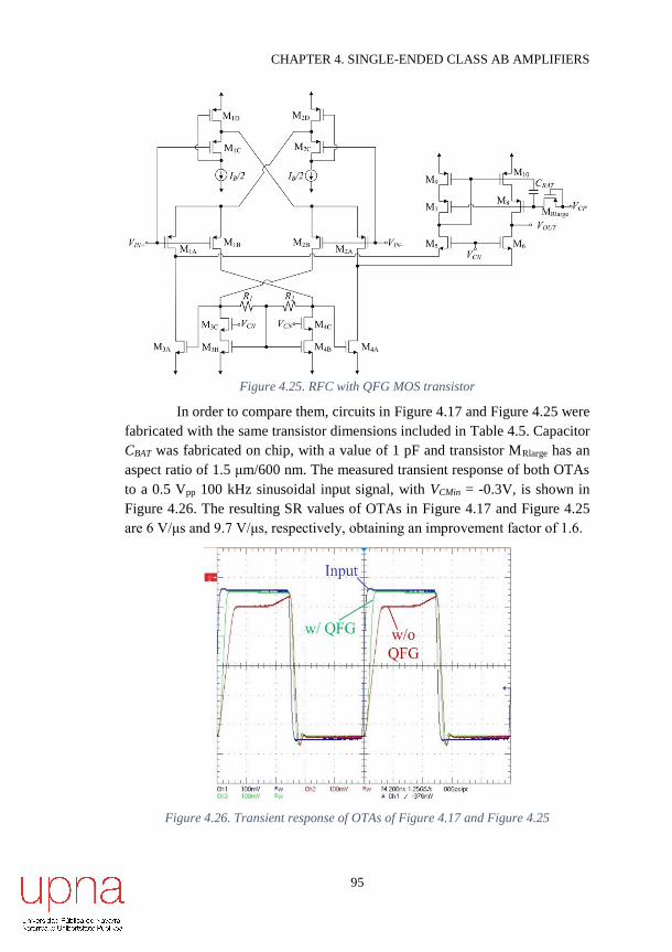
CHAPTER 4. SINGLE-ENDED CLASS AB AMPLIFIERS
95
Figure 4.25. RFC with QFG MOS transistor
In order to compare them, circuits in Figure 4.17 and Figure 4.25 were
fabricated with the same transistor dimensions included in Table 4.5. Capacitor
CBAT was fabricated on chip, with a value of 1 pF and transistor MRlarge has an
aspect ratio of 1.5 μm/600 nm. The measured transient response of both OTAs
to a 0.5 Vpp 100 kHz sinusoidal input signal, with VCMin = -0.3V, is shown in
Figure 4.26. The resulting SR values of OTAs in Figure 4.17 and Figure 4.25
are 6 V/μs and 9.7 V/μs, respectively, obtaining an improvement factor of 1.6.
Figure 4.26. Transient response of OTAs of Figure 4.17 and Figure 4.25

CHAPTER 4. SINGLE-ENDED CLASS AB AMPLIFIERS
96
As for the open loop parameters, both circuits present the same values,
which are included in Table 4.8, since the QFG transistor has no impact in DC.
As it has been observed in this Section, the performance of the super
class AB RFC OTA of Figure 4.17 strongly relies on the resistance value R of
two matched passive resistors, which can suffer from process and temperature
variations. Moreover, R can be chosen to optimize SR, GBW and phase margin
for a given load capacitance CL. Since R is fixed once the OTA is fabricated, the
use of a different CL leads to a suboptimal performance. Moreover, R in
Figure 4.17 was implemented using a high resistance non-silicided polysilicon
layer which may not be available in some low-cost CMOS processes.
A simple modification which solves these issues is proposed in
Figure 4.27. Active resistors replace these passive resistors, leading to a more
flexible approach able to adapt to process and temperature variations and to
different load conditions, and requiring less silicon area and no high resistive
layer.
In this design, local common mode feedback is implemented by
matched transistors MR1-MR2 operating in triode region as active resistors. When
the differential input signal is null, there is no current flowing through MR1-MR2
and the circuit in Figure 4.27 behaves as the RFC OTA in Figure 4.16(b), with
the same well-defined quiescent currents. However, with a differential input
voltage Vid > 0, there are identical voltage drops in MR1 and MR2 leading to an
increase in the VGS of M3A and a decrease in the VGS of M4A, thus causing a large
output current flowing to the load. For negative differential input voltages
(Vid < 0), a large current sinks from the load due to the decrease in VGS,3A and the
increase of VGS,4A.

CHAPTER 4. SINGLE-ENDED CLASS AB AMPLIFIERS
97
Figure 4.27. Class AB RFC with variable LCMFB resistors
The expressions for the GBW and SR of the OTA in Figure 4.27 are:
𝐺𝐵𝑊 ≈2𝑔𝑚1𝐴
2𝜋𝐶𝐿[1 + 𝑔𝑚3𝐴𝑅𝐷𝑆] (4.25)
𝑆𝑅 ≈𝛽3𝐴,4𝐴
2𝐶𝐿(√
𝛽1𝐵,2𝐵
2𝛽3𝐵,4𝐵𝐴 +
𝑅𝐷𝑆𝛽1𝐵,2𝐵
4𝐴2)
2
(4.26)
being A the amplitude of the differential input step and RDS the drain source
resistance of MR1 and MR2, which is controlled by DC voltage VBIAS:
𝑅𝐷𝑆 ≈1
𝛽𝑅1,2(𝑉𝐵𝐼𝐴𝑆−𝑉𝐺,3𝐵−𝑉𝑇𝐻)=
1
𝛽𝑅1,2(𝑉𝐵𝐼𝐴𝑆−√𝐼𝐵
𝛽3𝐵−𝑉𝑆𝑆−2𝑉𝑇𝐻)
(4.27)
Note that the larger RDS, the greater GBW and SR, but at the same time,
PM is degraded, as it happened in the OTA of Figure 4.17. For moderately large
RDS (few kΩ) the lowest non-dominant pole (gate node of M3A,4A) becomes
ωpND ≈ -1/(RDS·Cgs3A) and the phase margin is defined by:
𝑃𝑀 ≈ 90º − tan−1 (𝐺𝐵𝑊
𝑓𝑝𝑁𝐷
)
≈ 90º − tan−1 2𝑔𝑚1𝐴𝑅𝐷𝑆𝐶𝑔𝑠3𝐴
𝐶𝐿[1 + 𝑔𝑚3𝐴𝑅𝐷𝑆] (4.28)

CHAPTER 4. SINGLE-ENDED CLASS AB AMPLIFIERS
98
Thus, adjusting VBIAS (hence RDS) not only permit the optimization of
GBW, SR and PM for a given CL but also the compensation from process or
temperature variations.
A test chip prototype was fabricated in the previous 0.5 μm CMOS
process including the OTAs of Figure 4.16(a), Figure 4.16(b) and Figure 4.27.
Transistor aspect ratios are those previously used and listed in Table 4.4. The
aspect ratio of MR1 and MR2 is 30 μm/1 μm. Figure 4.28 shows the
microphotograph of the OTA of Figure 4.27. Supply voltage was 1 V,
IB = 10 A, VCP =-0.5V and VCN = 0.3V. An external load capacitor of 47 pF
was employed, which added to the capacitance of the test setup (pad, board and
test probe) leads to CL ≈ 70 pF.
Proposed OTA
10
0 µ
m
Figure 4.28. Microphotograph of the OTA of Figure 4.27
The simulated GBW and PM for VBIAS between 0.6 V and 0.9 V is plot
in Figure 4.29. As expected from Expressions 4.25, 4.26 and 4.28, GBW is
inversely proportional to VBIAS and PM decreases for lower VBIAS (i.e., larger
RDS).
Figure 4.29. GBW and PM vs VBIAS
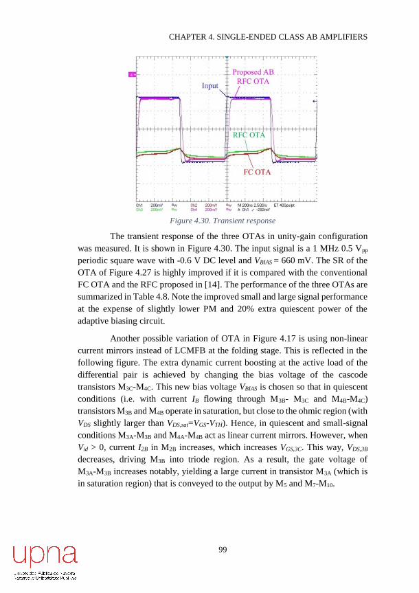
CHAPTER 4. SINGLE-ENDED CLASS AB AMPLIFIERS
99
Figure 4.30. Transient response
The transient response of the three OTAs in unity-gain configuration
was measured. It is shown in Figure 4.30. The input signal is a 1 MHz 0.5 Vpp
periodic square wave with -0.6 V DC level and VBIAS = 660 mV. The SR of the
OTA of Figure 4.27 is highly improved if it is compared with the conventional
FC OTA and the RFC proposed in [14]. The performance of the three OTAs are
summarized in Table 4.8. Note the improved small and large signal performance
at the expense of slightly lower PM and 20% extra quiescent power of the
adaptive biasing circuit.
Another possible variation of OTA in Figure 4.17 is using non-linear
current mirrors instead of LCMFB at the folding stage. This is reflected in the
following figure. The extra dynamic current boosting at the active load of the
differential pair is achieved by changing the bias voltage of the cascode
transistors M3C-M4C. This new bias voltage VBIAS is chosen so that in quiescent
conditions (i.e. with current IB flowing through M3B- M3C and M4B-M4C)
transistors M3B and M4B operate in saturation, but close to the ohmic region (with
VDS slightly larger than VDS,sat=VGS-VTH). Hence, in quiescent and small-signal
conditions M3A-M3B and M4A-M4B act as linear current mirrors. However, when
Vid > 0, current I2B in M2B increases, which increases VGS,3C. This way, VDS,3B
decreases, driving M3B into triode region. As a result, the gate voltage of
M3A-M3B increases notably, yielding a large current in transistor M3A (which is
in saturation region) that is conveyed to the output by M5 and M7-M10.

CHAPTER 4. SINGLE-ENDED CLASS AB AMPLIFIERS
100
Figure 4.31. Class AB RFC with non-linear current mirror at the load stage
An approximate analytical expression for the output current Iout when
Vid > 0 can be obtained using the simple square-law MOS model for strong
inversion and saturation region and the expression for ohmic region and low VDS
given by ID = ·(VGS – VTH)·VDS. The resulting current in M3A is
𝐼3𝐴 =𝛽3𝐴
2(
𝐼2𝐵
𝛽3𝐵𝑉𝐷𝑆,3𝐵)
2
(4.29)
where 𝑉𝐷𝑆,3𝐵 = 𝑉𝐵𝐼𝐴𝑆 − √2𝐼2𝐵 𝛽3𝐶⁄ − 𝑉𝑇𝐻. Expressing I2B as a function of Vid,
current I3A becomes
𝐼3𝐴 =𝛽3𝐴
2[
𝛽2𝐵
2𝛽3𝐵𝑉𝐷𝑆,3𝐵(√
𝐼𝐵
𝛽1𝐵+ 𝑉𝑖𝑑)
2
]
2
(4.30)
For a large positive differential input step of A Volts current in M1A and
M4A is very low and M2A enters deep triode region, so Iout I3A and
𝑆𝑅+ ≈𝛽3𝐴
2𝐶𝐿[
𝛽2𝐵
2𝛽3𝐵𝑉𝐷𝑆,3𝐵𝐴2]
2
≈𝐾
8𝐶𝐿
𝛽2𝐵2
𝛽3𝐵𝑉𝐷𝑆,3𝐵2 𝐴4 (4.31)
Analogously, for Vid < 0:
𝐼4𝐴 =𝛽4𝐴
2[
𝛽1𝐵
2𝛽4𝐵𝑉𝐷𝑆,4𝐵(√
𝐼𝐵
𝛽2𝐵+ 𝑉𝑖𝑑)
2
]
2
(4.32)

CHAPTER 4. SINGLE-ENDED CLASS AB AMPLIFIERS
101
and for a large negative differential input step of -A Volts, Iout I4A and
𝑆𝑅− ≈𝛽4𝐴
2𝐶𝐿[
𝛽1𝐵
2𝛽4𝐵𝑉𝐷𝑆,4𝐵𝐴2]
2
≈𝐾
8𝐶𝐿
𝛽1𝐵2
𝛽4𝐵𝑉𝐷𝑆,4𝐵2 𝐴4 (4.33)
In practice SR is lower due to second-order effects not considered in
the analysis and since transistors operating in saturation may leave this region
for large inputs. Note however that a large SR compatible with low static power
is achieved as SR is not proportional to IB.
A simple and robust way to generate VBIAS is shown in Figure 4.31.
Choosing IB’ and the W/L of M11 correctly, VDS3B,4B can be set slightly above
VDS,sat regardless of process, temperature or supply voltage variations as VBIAS is
set by the VGS of a scaled replica of M3B-M4B.
The adaptive bias current source employed also improves GBW, as the
full differential input signal is applied to each input transistor [1].
OTAs of Figure 4.16(a), Figure 4.16(b) and Figure 4.31 were included
on a 0.5 μm CMOS chip prototype. The aspect ratio of every transistors except
for M11 are that on Table 4.4, and that of M11 is 15 m/0.6 m. Figure 4.32
shows a microphotograph of the three OTAs. Supply voltage was set to 1V,
IB = IB’ = 10 A, VCP = -0.5 V and VCN = 0.3 V.
Figure 4.32. Microphotograph of OTAS in Figure 4.16(a), Figure 4.16(b)
and Figure 4.31

CHAPTER 4. SINGLE-ENDED CLASS AB AMPLIFIERS
102
Figure 4.33. Transient response of OTAs of Figure 4.16(a), Figure 4.16(b)
and Figure 4.31
The measured transient response in voltage follower configuration of
the three OTAs is shown in Figure 4.33. An external load capacitor of 47 pF was
connected. However, including the capacitance of the test setup (pad, board and
test probe), the overall load capacitance is CL ≈ 70 pF. The input signal was a
1 MHz 0.5 V periodic square wave, whose DC level was -0.6 V. Table 4.8
summarizes the main measured performance parameters. Note an improved SR
by a factor of 28 versus the FC OTA.
In addition, the figures of merit previously defined are included in
Table 4.8. Note that the proposed OTA shows competitive small-signal and
large-signal performance.
Thus, proper biasing of the differential pair active load in the RFC OTA
can provide dynamic current boosting in a simple way. Together with an
adaptive biasing current source, efficient super class AB operation can be
achieved.

CHAPTER 4. SINGLE-ENDED CLASS AB AMPLIFIERS
103
Figure 4.34. Class AB RFC with WTA scheme at the input stage
Another alternative topology is obtained by modifying the adaptive
biasing scheme of Figure 4.17 by a Winner-Take-All (WTA) configuration,
previously explained in Chapter 2. Figure 4.34 shows the complete schematic
of this amplifier. As it was mentioned in Section 2.2.3.2, dynamic currents
achieve with the WTA scheme are the same as that of cross-coupled floating
batteries, hence the same SR equation of Figure 4.17 applies in this case (see
expression 4.23 and 4.24). However, since the common source node behaves as
a virtual ground, the transconductance is not improved when compared with
conventional class A amplifier. Thus, the transconductance (so as GBW) of
op-amp of Figure 4.34 is half of that of Figure 4.17, i.e.
GBW = gm1A·[1+gm3A(R||ro2B)], which leads to a 6 dB decrease in the DC gain.
Transistors sizes of this OTAs are that in Table 4.4. Supply voltages
are set to ± 1V, and bias current IB is 10 𝜇A. Cascode voltages VCP and VCN are
-0.5 V and 0.3 V respectively.
The transient response of the Class A Folded Cascode, conventional
Class A RFC and the amplifier of Figure 4.34 to a 0.5 Vpp 1 MHz square signal
was measured and plot in figure below. The input common mode is
VCMin = -0.6 V. It can be seen that the transient response of the amplifier of
Figure 4.34 is improved, but settling performance is worse than with the
previously used adaptive biasing scheme. This may be due to the lower speed of

CHAPTER 4. SINGLE-ENDED CLASS AB AMPLIFIERS
104
the WTA circuit for large inputs (which can drive M1D and M2D near triode
region).
Figure 4.35. Transient response of the WTA class AB RFC
As for the small signal parameters, the simulated values are included in
Table 4.8. As it was mentioned before, the ADC is 6 dB below that of Figure 4.17
and GBW is half of that of Figure 4.17.
Another variation of the amplifier of Figure 4.17 is depicted in
Figure 4.36. In this case, the drains of transistors M1A and M2A are not connected
to that of M3A and M4A, but to that of M1B and M2B, respectively. Since they are
connected in parallel, they behave as a single transistor with twice the size. In
addition, the dimensions of M3A, M3B, M4A and M4B have been changed so that
the power consumption of OTA of Figure 4.36 is the same as that of
Figure 4.16(a), that is, now the four transistors have the same dimensions. The
resulting circuit corresponds to the conventional super class AB (symmetrical
current mirror) OTA [1].

CHAPTER 4. SINGLE-ENDED CLASS AB AMPLIFIERS
105
Figure 4.36. An alternative super class AB RFC OTA
The transconductance, output resistance and GBW of the above
amplifier are
𝐺𝑚 = 2(𝑔𝑚1𝐴 + 𝑔𝑚1𝐵)𝑔𝑚3𝐴(𝑅‖𝑟𝑜2𝐴‖𝑟𝑜2𝐵) = 4𝑔𝑚1𝐴𝑔𝑚3𝐴(𝑅‖(𝑟𝑜2𝐵/2))
(4.34)
𝑅𝑜𝑢𝑡 ≈ 𝑔𝑚6𝑟𝑜6𝑟𝑜4𝐴‖𝑔𝑚8𝑟𝑜8𝑟𝑜10 (4.35)
𝐺𝐵𝑊 =4𝑔𝑚1𝐴𝑔𝑚3𝐴(𝑅‖(𝑟𝑜2𝐵/2))
2𝜋𝐶𝐿 (4.36)
Although there is an increase factor of 2 when comparing Equations
4.34 and 4.12, gm3A is √2/3 of the gm3A of Figure 4.17, so the net factor is
2√2/3=0.94 due to the resizing. Note that R||(ro2B/2) can be as low as half of the
value of (R||ro2B), depending of the value of R and ro2B. Since the value of R
cannot be increased with no limit, due to the non-dominant pole introduced by
the active current mirror (ωp3 ≈ −1/[(R||ro2B)Cgs3A]) usually R<<ro2B and similar
values of Gm (thus GBW) can be obtained for both amplifiers in Figure 4.17 and
Figure 4.36.
As for the output resistance, that of Figure 4.36 is greater than that of
Figure 4.17, since the term ro2B disappeared and ro4A is larger since M4A drives
2/3 less quiescent current in Figure 4.36. Thus, higher values of ADC can be
achieved.

CHAPTER 4. SINGLE-ENDED CLASS AB AMPLIFIERS
106
With a transient analysis similar to that of Appendix C, it can be
deduced that the theoretical value of the SR is
𝑆𝑅 ≈𝛽3𝐴
2𝐶𝐿(√
𝛽2𝐵
𝛽3𝐵𝐴 +
𝑅1𝛽2𝐵
2𝐴2)
2
(4.37)
In order to compare this expression with Equations 4.23 and 4.24, the
value of 3A in Figure 4.17 and Figure 4.36 are related as follows: 3A,17 =
3·3A,36. Hence, the following expression is obtained for the OTA of Figure 4.17:
𝑆𝑅 ≈𝛽3𝐴,36
3𝐶𝐿(√
𝛽2𝐵
2𝛽3𝐵,36𝐴 +
𝑅1𝛽2𝐵
2𝐴2)
2
(4.38)
It can be deduced that with high values of amplitude, larger SR can be
obtained for the same power consumption.
The OTA of Figure 4.36 was fabricated in the same 0.5 m CMOS
technology which has been used previously, along with the FC and conventional
RFC amplifiers. Table 4.6 contains the dimensions of the transistors.
Transistor W/L (μm/μm)
M1A-M2A 190/0.6
M1B-M2B 190/0.6
M1C-M2C 190/0.6
M1D-M2D 60/0.6
M3A-M4A 120/0.6
M3B-M4B 60/0.6
M3C-M4C 120/0.6
M5-M6 120/0.6
M7-M8 200/0.6
M9-M10 200/0.6
Table 4.6. Transistors aspect ratio of opamp in Figure 4.36

CHAPTER 4. SINGLE-ENDED CLASS AB AMPLIFIERS
107
Figure 4.37. Transient response of the amplifier in Figure 4.36
The transient response of the amplifier in Figure 4.36 is plot in
Figure 4.37, along with that of conventional FC and RFC OTAs. The input
voltage was a 1 MHz 0.5 Vpp square signal, with an input DC level of
VCMin = -0.6 V. As it can be seen in figure above, the proposed circuit can follow
the input signal, whereas the conventional FC and RFC class A amplifiers
cannot. Note that the amplitude of the output signal reaches the maximum
amplitude, i.e. that of the input signal.
Finally, Figure 4.38 shows the last alternative to the RFC of
Figure 4.17. Despite the improved small-signal and large-signal performance of
the super class AB RFC OTA in Figure 4.17, it is still limited by various reasons.
First, cascode transistors are biased with constant voltages, which limits the VDS
of the transistors connected to their source and that therefore can make these
transistors enter triode region for large dynamic currents. This fact can restrict
the maximum dynamic currents and hence degrade SR notably [27]. The
modification in Figure 4.25 alleviates this problem but cascode transistors M5
and M6 are still biased with constant voltage. Second, the bottom current mirrors
still scale the quiescent currents by factor K. The amplifier proposed in
Figure 4.38 overcomes these drawbacks, improving both small-signal and large-
signal performance for the same quiescent power consumption and supply
voltage requirements.

CHAPTER 4. SINGLE-ENDED CLASS AB AMPLIFIERS
108
Figure 4.38. Enhanced super class AB RFC OTA
Two main improvements are included versus the OTA in Figure 4.17.
First, based on [15], current mirrors IB/4 are connected to the drains of M1B and
M2B. This reduces the quiescent current of M3B-M4B from IB/2 to IB/4, allowing
to use a K=6 (instead of K=3) at the bottom current mirrors M3A-M3B and
M4A-M4B for the same quiescent current consumption. As a result, the
expressions for transconductance and GBW of the OTA in Figure 4.38 are the
same as that of the OTA in Figure 4.17. (see Expressions 4.12 and 4.18).
However, an increase factor of 1.41 is obtained, since gm3A increases by the same
factor. Hence this modification improves small-signal performance preserving
quiescent currents.
The second improvement concerns large signal operation. The
theoretical positive and negative SR of the RFC in Figure 4.17 are defined by
Expression 4.23 and 4.24, respectively. However, in practice lower values are
achieved mainly because transistors M3A, M4A, M9 and M10 may enter triode
region for large A values. This is due to cascode transistors M5, M6, M7 and M8
which restrict their VDS. This limitation is very relevant with the low supply
voltages employed nowadays in advanced technology nodes, which notably

CHAPTER 4. SINGLE-ENDED CLASS AB AMPLIFIERS
109
restrict the maximum cascode bias voltages. The solution employed here is the
use of dynamic biasing of the cascode transistors using Quasi-Floating Gate
(QFG) techniques [20], [27], as shown in Figure 4.38. Three capacitors CBAT are
included that connect the gates of M3A-M5, M4A-M6 and M9,10-M7,8. Minimum-
size PMOS transistors MP1, MP2 and MP3 act as high resistance pseudo-resistors
for DC biasing of the cascode transistors. In quiescent operation capacitors CBAT
behave as open circuits and no current flows through the pseudo-resistors, so
cascode bias voltages are VCP and VCN, just like in Figure 4.16(b). However, for
a large positive differential input voltage, the voltage at the gate of M3A
increases. Since CBAT cannot discharge fast, it acts as a floating battery that
translates this voltage increase to the gate of M5. This way the VDS of M3A
increases, allowing to drive a large current without entering triode region.
Similarly, the decrease of the gate voltage of M9-M10 produced by this large
current is translated to the gate of M7-M8, increasing the VSD of M9-M10. For a
large negative differential input voltage, the voltage at the gate of M4A increases
and this increase is translated to the gate of M6, leading to a larger VDS in M4A
that allows sinking a large current from the load as M4A does not enter triode
region.
Both amplifiers of Figure 4.16(b) and Figure 4.38 were designed and
fabricated in a GlobalFoundries 130 nm 8-metal CMOS technology. Resistors
R1 and R2 of 20 kΩ were made by a high resistance silicided polysilicon layer
available in the technology. Conventional matching enforcement techniques
were used for the transistors and resistors. Dual nitride MiM capacitors with
nominal capacitance of 500 fF were used to implement CBAT. A chip
microphotograph is shown in Figure 4.39. Since the top passivation layer is
opaque in this process, the designed layout has been superimposed. Transistor
aspect ratios are summarized in Table 4.7.

CHAPTER 4. SINGLE-ENDED CLASS AB AMPLIFIERS
110
Class A
Class AB
100 µm
Figure 4.39. Test chip microphotograph
The OTAs of Figure 4.16(b) and Figure 4.38 were measured in
unity-gain closed loop configuration using a dual supply voltage of 0.5 V and
a bias current IB = 3 A.
Transistor W/L (μm/μm)
M1A-M2A 12/0.24
M1B-M2B 12/0.24
M1C-M2C 12/0.24
M1D-M2D 12/0.24
M3A-M4A 72/0.24
M3B-M4B 12/0.24
M3C-M4C 12/0.24
M5-M6 24/0.24
M7-M8 12/0.12
M9-M10 12/0.24
MR1, MR2, MR3 0.16/0.12
Table 4.7. Transistor Aspect Ratios of opamps of Figure 4.16(b) and Figure 4.38
For time-domain measurements, an external ceramic load capacitor of
47 pF was connected to the output. The total capacitance also includes the
capacitance of the pad, package traces, PCB plating bus and active probe, and
its estimated value is CL = 70 pF. For frequency-domain measurements, the same
47 pF ceramic capacitor was used at the output, but now an external wideband
buffer was employed. Hence the total capacitance includes the load, pad,

CHAPTER 4. SINGLE-ENDED CLASS AB AMPLIFIERS
111
package traces, PCB plating bus and buffer input capacitances. The total
estimated value is CL = 50 pF.
Figure 4.40 shows the response of the RFC OTA of Figure 4.16(b) and
the super class AB RFC OTA of Figure 4.38 to a 1 MHz 0.4 V periodic square
input signal, also shown in the figure. The DC input level was set to 0 V. Note
the improved dynamic performance of the proposed OTA of Figure 4.38. The
measured average SR = (SR++SR-)/2 of the RFC OTA of Figure 4.16(b) is
0.194 V/s and that of the proposed OTA of Figure 4.38 is 19.26 V/s, i.e.,
almost 100 times higher.
Figure 4.40. Measured response of the RFC and super class RFC OTAs
to a square input signal
The frequency response of both circuits as voltage followers is shown
in Figure 4.41. The measured bandwidth corresponds to the OTA unity-gain
frequency and to the GBW since the non-dominant poles are above this
frequency. The circuit of Figure 4.16(b) has a f-3dB= 380 kHz and the circuit of
Figure 4.38 has a f-3dB= 10.43 MHz, i.e., an increase factor of 27.
0 0.2 0.4 0.6 0.8 1 1.2 1.4 1.6 1.8 2
x 10-6
-0.2
-0.1
0
0.1
0.2
Time (s)
Am
plit
ude (
V)
input
superclass AB
class A

CHAPTER 4. SINGLE-ENDED CLASS AB AMPLIFIERS
112
Figure 4.41. Measured frequency response of both OTAs connected
as voltage followers
The measured Total Harmonic Distortion (THD) of both circuits is
shown in Figure 4.42. A single input tone of 10 kHz and peak-to-peak amplitude
ranging from 100 mV to 450 mV has been used. The low frequency employed
is due to the low bandwidth of the class A RFC OTA of Figure 4.16(b) which
does not allow comparison at high frequencies. Note that the OTA of
Figure 4.38 achieves lower distortion, mainly due to the increased
transconductance achieved, as previously mentioned.
Figure 4.42. Measured THD vs input amplitude of the RFC and
super class AB RFC OTAs
104
105
106
107
-20
-15
-10
-5
0
5
Frequency (Hz)
Gain
(dB
)
class A super class AB
100 150 200 250 300 350 400 450-75
-70
-65
-60
-55
-50
-45
-40
Input amplitude (mVpp)
TH
D(d
B)
super class AB
class A

CHAPTER 4. SINGLE-ENDED CLASS AB AMPLIFIERS
113
The main measurement results of both OTAs are included in Table 4.8.
Note the improved small-signal and large-signal operation of the proposed super
class AB RFC OTA. To allow a simpler comparison, the previously defined
Figures of Merit have been employed. Note that the proposed OTA shows
improved performance for both FoMs. The drawbacks of the proposed circuit
are the increased area requirements (mainly due to capacitors CBAT) and a 25%
increase in static power consumption versus the RFC OTA of Figure 4.16(b).
4.2 Comparison of the Class AB Amplifiers
In this Chapter, several amplifiers have been proposed, all of them with
different features. The purpose of this section is to compare them and highlight
their benefits and disadvantages, and their possible applications. Besides, other
amplifiers previously published have been included in order to put together the
state of the art and have a global point of view.
Table 4.8 sums up the parameters of the different op-amps. Note that
four different technologies have been employed to fabricate the amplifiers:
0.5 m, 0.35 m, 0.18 m and 0.13 m. Besides, amplifiers proposed in [7], [8]
and [26] employ differential topologies, which present higher Gm when
compared to their respective single-ended version.
As for the SR, the greater value is obtained by [26]. However, its power
consumption is much higher (in the order of mW) than the ones in this thesis
(around 100 W). Among the amplifiers proposed in this work, the amplifier of
Figure 4.27 presents the higher SR, due to its adaptive local common-mode
feedback (LCMFB) scheme, making this alternative a flexible solution. For
fixed RLCMFB schemes, Figure 4.17, Figure 4.34 and Figure 4.36 achieve also
very large output currents.
Regarding the small signal parameters, the amplifier in [26] has the
greatest GBW, but again, its power consumption is much higher. If the
amplifiers proposed in this thesis are considered, the opamp of Figure 4.38 has
the greatest GBW, due to the fact that it was fabricated in a 0.13 m. For a
0.5 m technology, the circuit proposed in Figure 4.8 has the biggest GBW and
ADC values of the proposed topologies. However, its transient behavior is not as
good as other proposed OTAs, such as Figure 4.17. This fact makes amplifier in
Figure 4.8. Proposed class AB folded cascode OTA

CHAPTER 4. SINGLE-ENDED CLASS AB AMPLIFIERS
114
suitable for applications which requires a good small-signal performance, while
not needing large dynamic output currents.
For a more understandable comparison, the two figures of merit
previously employed are calculated for every amplifier: a large-signal FoM,
FoML = SR·CL/Isupply=ImaxL/Isupply, where Isupply is the total current consumption,
which represents the large-signal current efficiency, and a small-signal FoM,
FoMS=100·GBW·CL/Isupply (MHz·pF/μA), which shows the small-signal
speed/power ratio. Figure 4.43 represents both large and small signal Figures of
Merit for the amplifiers in Table 4.8. Logarithmic axes are employed so that the
points are clearly shown. For both FoMs, the higher values, the better
performance the amplifier has. Thus, the target is to place the amplifiers in the
upper right corner. As it can be seen from that figure, the FoM values of the
proposed amplifiers are higher than those of the state of the art. Note the great
improvement achieved by the amplifier of Figure 4.38, due to the use of a
0.13 m technology. This fact confirms that the advantages of the proposed
techniques (mainly tested in a 0.5 𝜇m process) also apply in more modern
technology nodes.
The small-signal FoM of Figure 4.23 and Figure 4.34 are lower than
the rest of the proposed amplifiers. The reason of their relatively low FoMS is
that they do not use adaptive biasing techniques which double the
transconductance. In the case of Figure 4.23 (with and without QFG), they use
a conventional transistor acting as current source, and Figure 4.34 uses a WTA
scheme, which provides large dynamic current but it does not increase the Gm.
Figure 4.43. Performance comparison using two FoM

CHAPTER 4. SINGLE-ENDED CLASS AB AMPLIFIERS
115
FoM
S
54.3
554
92.8
171.5
532
176.8
274.8
446.6
434
350
FoM
L
0,5
6
11.4
3
0.3
5
0.6
7
18.4
8
0.8
1
1.5
9
13.5
8
6.7
2
22.4
6
Are
a
(mm
2)
0.0
20
0.0
24
0.0
22
0.0
26
0.0
30
0.0
28
0.0
28
0.0
26
0.0
25
0.0
25
Po
wer
(μW)
80
12
0
80
80
10
0
80
80
10
0
10
0
10
0
Eq
. in
pu
t
no
ise
*
@1
MH
z
(nV
/H
z)
49
35
22
19
15
36
35
22
.8
22
.8
23
GB
W
(MH
z)
0.3
1
4.7
5
0.5
3
0.9
8
3.8
1.0
1
1.5
7
3.1
9
3.1
0
2.5
PM
*
(º)
89
60
89
86
.7
75
.1
86
.3
80
.1
77
.4
77
.6
81
.3
AD
C*
(dB
)
69
81
.7
60
.3
68
.4
76
.8
68
.7
73
.4
77
.6
77
.6
76
.4
TH
D
(dB
)
-24
@
100kH
z
1 V
pp
-41
@
100kH
z
1 V
pp
-37
.8
@ 2
5 k
Hz
0.5
Vp
p
-47
.4
@ 2
5 k
Hz
0.5
Vpp
-55
.5
@ 2
5 k
Hz
0.5
Vp
p
-47
.3
@ 2
5 k
Hz
0.5
Vp
p
-50
.2
@ 2
5 k
Hz
0.5
Vp
p
-57
.02
@
25 k
Hz
0.5
Vp
p
-56
.94
@
25 k
Hz
0.5
Vp
p
-45
.5
@ 2
5 k
Hz
0.5
Vp
p
t set
tl-
(ns)
--
74
18
40
56
0
10
0
10
7
16
5
94
.4
10
1
--
t set
tl+
(ns)
--
96
27
00
17
20
12
0
14
00
92
0
38
0
49
6
--
SR
-
(V/μs)
-0.2
8
-7.6
-0.6
6
-1.5
-25.3
-20.1
-24.3
-16.5
-14.5
-18.2
SR
+
(V/μs)
0.3
2
9.8
0.2
0
0.3
8
13.2
0.4
6
0.9
1
10.2
6.9
16.0
4
CL
(pF
)
70
70
70
70
70
70
70
70
70
70
CM
OS
tech
.
(μm)
0.5
0.5
0.5
0.5
0.5
0.5
0.5
0.5
0.5
0.5
Fig
ure
4.7
(a)
Fig
ure
4.8
Fig
ure
4.1
6(a
)
Fig
ure
4.1
6(b
)
Fig
ure
4.1
7
Fig
ure
4.2
3
R=
10
k
Fig
ure
4.2
3
R=
20
k
Fig
ure
4.2
5
w/
QF
G
Fig
ure
4.2
5 w
/o
QF
G
Fig
ure
4.2
7

CHAPTER 4. SINGLE-ENDED CLASS AB AMPLIFIERS
116
FoM
S
476
220
434
3477
30.4
22.7
88.9
165.4
70
261.7
FoM
L
10.1
8
17.7
8
19.8
8
89.8
8
0.7
5
0.2
6
0.1
9
0.9
9
0.3
9
2.2
4
Are
a
(mm
2)
0.0
2
0.0
28
0.0
28
0.0
02
0.0
57
0.0
26
0.1
57
0.0
20
0.0
29
0.0
70
Po
we
r
(μW)
10
0
10
0
10
0
15
1.2
11
0
19
7
25
.4
43
7.5
11
90
0
Eq
. in
pu
t
no
ise
*
@1
MH
z
(nV
/H
z)
22
31
.4
21
41
--
80
<6
0
10
0
--
--
GB
W
(MH
z)
3.4
1.5
7
3.1
10
.43
0.0
57
2.5
11
.67
3
4.9
86
.5
PM
*
(º)
76
.3
84
.5
72
.4
88
.8
60
--
66
.1
60
83
50
AD
C*
(dB
)
75
.1
70
.7
78
.8
56
.7
51
52
88
.3
57
.5
63
.4
72
TH
D (
dB
)
-47
.85
@
25 k
Hz
0.5
Vp
p
-48
.54
@
25 k
Hz
0.5
Vp
p
-56
.1
@ 2
5 k
Hz
0.5
Vp
p
-51
@
10 k
Hz
0.4
Vp
p
-52
@
1 k
Hz,
0.5
Vp
p
-40
@
0.4
Vp
p
--
-40
.1
@250 k
Hz
0.4
Vp
p
-47
.1
@ 2
Vp
p
--
t set
tl-
(ns)
13
0
71
--
--
--
10
00
--
--
t set
tl+
(ns)
42
0
90
--
--
22
4
13
00
--
--
SR
-
(V/μs)
-18.8
-23.1
-26.8
-34.8
--
--
-1.3
7
-3.8
-3.3
--
SR
+
(V/μs)
7.2
7
12.7
14.2
3.7
2
0.1
4
2.8
9
2.5
3
1.8
2.7
74.1
CL
(pF
)
70
70
70
70/
50
8
20
15
20
25
200
CM
OS
tech
.
(μm)
0.5
0.5
0.5
0.1
3
0.1
8
0.1
8
0.3
5
0.1
8
0.5
0.1
8
Fig
ure
4.3
1
Fig
ure
4.3
4
Fig
ure
4.3
6
Fig
ure
4.3
8
[6]
[7]
[8]
[9]
[25
]
[26
]
*S
imu
lati
on
Ta
ble
4.8
. S
um
ma
ry o
f m
easu
rem
ent
resu
lts
an
d p
erfo
rman
ce
com
pa
riso
n

CHAPTER 4. SINGLE-ENDED CLASS AB AMPLIFIERS
117
4.3 Conclusions
In this chapter, different single-ended amplifiers have been proposed.
They are based on three of the most important OTA topologies: the telescopic
cascode amplifier, the folded cascode and the recycling folded cascode.
Different mathematical analysis were developed to prove the enhancement in
different parameters, such as DC gain, GBW, SR and noise.
Different prototype chips were fabricated in two technologies (0.5 μm
and 0.13 μm) in order to provide experimental measurements. All of them
improve the performance of the conventional amplifiers.

CHAPTER 4. SINGLE-ENDED CLASS AB AMPLIFIERS
118
Bibliography of the Chapter
[1] A.J. Lopez-Martin, S. Baswa, J. Ramirez-Angulo and R. G. Carvajal,
“Low-voltage super class AB CMOS OTA cells with very high slew
rate and power efficiency”, IEEE Journal of Solid-State Circuits,
vol. 40, no. 5, pp. 1068-1077, 2005.
[2] J. A. Galan, A. J. Lopez-Martin, R. G. Carvajal, J. Ramirez-Angulo and
C. Rubia-Marcos, “Super class-AB OTAs with adaptive biasing and
dynamic output current scaling”, IEEE Transactions on Circuits and
Systems I: Regular Papers, vol. 54, no. 3, pp. 449-457, 2007.
[3] J. Baker, “CMOS circuit design, layout and simulation”, Wiley
Editorial, 3rd Edition, p. 733, 2010.
[4] S. Baswa, J. Ramirez-Angulo, A. Lopez-Martin, R. G. Carvajal and
M. Bikumandla, “Rail-to-rail super class AB CMOS operational
amplifiers”, Electronics Letters, vol. 41, no. 1, pp. 1-2, 2005.
[5] J. Ramirez-Angulo, M. Sawant, A. Lopez-Martin and R. G. Carvajal,
“A power efficient and simple scheme for dynamically biasing cascode
amplifiers and telescopic op-amps”, The VLSI Journal Integration,
vol. 41, no. 4, pp. 539-543, 2008.
[6] M. R. Valero Bernal, S. Celma, N. Medrano and B. Calvo, “An
ultralow-power low-voltage class-AB fully differential opamp for
long-life autonomous portable equipment”, IEEE Transactions on
Circuits and Systems II: Express Briefs, vol. 59, no. 10, pp. 643-647,
2012.
[7] S. Chatterje, Y. Tsividis and P. Kinget, “A 0.5-V bulk-input fully
differential operational transconductance amplifier”, Proceedings of
the 30th European Solid-State Circuits Conference (ESSCIRC),
pp. 147-150, Leuven, Belgium, 2004.
[8] L. Zuo and S. K. Islam, “Low-voltage bulk-driven operational
amplifier with improved transconductance”, IEEE Transactions on
Circuits and Systems I: Regular Papers, vol. 60, no. 8, pp. 2084-2091,
2013.

CHAPTER 4. SINGLE-ENDED CLASS AB AMPLIFIERS
119
[9] E. Cabrera-Bernal, S. Pennisi, A. D. Grasso, A. Torralba and
R. G. Carvajal, “0.7-V three-stage class-AB CMOS Operational
Transconductance Amplifier”, IEEE Transactions on Circuits and
Systems I: Regular Papers, vol. 63, no. 11, pp. 1807-1815, 2016.
[10] J. M. Saso, A. Lopez-Martin, M. P. Garde and J. Ramirez-Angulo,
“Power-efficient class AB fully differential amplifier”, Electronics.
Letters, vol. 53, no. 19, pp. 1298-1300, 2017.
[11] K. de Langen and J.H. Huijsing, “Compact low-voltage power-efficient
operational amplifier cells for VLSI”, IEEE Journal of Solid-State
Circuits, vol. 33, no. 10, pp. 1482-1496, 1998.
[12] K. Nakamura and L.R. Carley, “An enhanced fully differential folded
cascode op amp”, IEEE Journal of Solid-State Circuits, vol. 27, no. 4,
pp. 563-568, 1992.
[13] J. Adut, J. Silva-Martinez and M- Rocha-Perez, “A 10.7 MHz sixth
order SC ladder filter in 0.35 um CMOS technology”, IEEE
Transactions on Circuits and Systems I: Regular Papers, vol. 53,
no. 8, pp. 1625-1635, Aug. 2006.
[14] R. Assaad and J. Silva-Martinez, “The recycling folded cascode: a
general enhancement of the folded-cascode amplifier”, IEEE Journal
of Solid-State Circuits, vol. 44, no. 9, pp. 2535-2542, 2009.
[15] Y.-L. Li, K.-F. Han, X. Tan, N. Yan and H. Min, “Transconductance
enhancement method for operational transconductance amplifiers”,
Electronics Letters, vol. 46, no. 19, pp.1330-1331, 2010.
[16] Z. Yan, P.-I. Mak and R. P. Martins, “Double recycling technique for
folded-cascode OTA”, Analog Integrated Circuits and Signal
Processing, vol. 71, no. 1, pp. 137-141, 2012.
[17] M. Yavari and T. Moosazadeh, “A single-stage operational amplifier
with enhanced transconductance and slew rate for switched-capacitor
circuits”, Analog Integrated Circuits and Signal Processing, vol. 79,
no. 3, pp. 589-598, 2014.
[18] V. Peluso, P. Vancorenland, M. Steyaert, and W. Sansen, “900mV
differential class AB OTA for switched opamp applications”,
Electronics Letters, vol. 33, no. 17, pp. 1455-1456, 1997.

CHAPTER 4. SINGLE-ENDED CLASS AB AMPLIFIERS
120
[19] R. G. Carvajal, J. Ramirez-Angulo, A. J. Lopez-Martin, A. Torralba,
J. A. Galan, A. Carlosena and F. M. Chavero, “The flipped voltage
follower: a useful cell for low-voltage low-power circuit design”, IEEE
Transactions on Circuits and Systems I: Regular Papers, vol. 52,
no. 7, pp. 1276-1291, 2005.
[20] J. Ramirez-Angulo, A. J. Lopez-Martin, R.G. Carvajal and
F. Muñoz-Chavero, “Very low voltage analog signal processing based
on Quasi Floating Gate transistors”, IEEE Journal of Solid-State
Circuits, vol. 39, no. 3, pp. 434-442, 2003.
[21] J. Ramirez-Angulo, R.G. Carvajal, J. A. Galan and A. Lopez-Martin,
“A free but efficient low-voltage class-AB two-stage operational
amplifier”, IEEE Transactions on Circuits and Systems II: Express
Briefs, vol. 53, no. 7, pp. 568-571, 2006.
[22] T.C. Carusone, D. Johns and K. Martin. “Analog integrated circuit
design”, Wiley, 2nd Edition, 2011.
[23] J. Ramirez-Angulo and M. Holmes, “Simple technique using local
CMFB to enhance slew rate and bandwidth of one-stage CMOS
op-amps”, Electronics Letters, vol. 38, pp. 1409-1411, 2002.
[24] A. J. Lopez-Martin, M. P. Garde and J. Ramirez-Angulo, “Class AB
differential difference amplifier for enhanced common-mode
feedback”, Electronics Letters, vol. 53, no. 7, pp. 454-456, 2017.
[25] P.R. Surkanti and P.M. Furth, “Converting a three-stage
pseudoclass-AB amplifier to a true-class-AB amplifier”, IEEE
Transactions on Circuits and Systems II: Express Briefs, vol. 59, no. 4,
pp. 229-233, 2012.
[26] S. Sutula, M. Dei, L. Teres and F. Serra-Graells, “Variable-mirror
amplifier: a new family of process-independent class-AB single-stage
OTAs for low-power SC circuits”, IEEE Transactions on Circuits and
Systems I: Regular Papers, vol. 63, no. 8, pp. 1101-1110, 2016.
[27] S. Pourashraf, J. Ramirez-Angulo, A. J. Lopez-Martin and R. G.
Carvajal, “Super class AB OTA without open‐loop gain degradation
based on dynamic cascode biasing”, International Journal of Circuit
Theory and Applications, vol. 45, no. 12, pp. 2111-2118, 2017.

121
Chapter 5
FULLY DIFFERENTIAL CLASS AB
AMPLIFIERS
In Chapter 4, several single-ended amplifiers have been presented.
However, fully differential topologies present some advantages versus their
single-ended version. Some of these benefits are:
Increased gain
Thanks to the change in phase between the differential outputs, the
amplitude of the output swing is doubled (i.e. an increase of 6 dB in voltage
gain) over a single-ended output, thus improving also dynamic range. This is a
clear positive point for low-voltage systems.
Improved common-mode rejection ratio (CMRR)
Ideally, the effect of the common-mode input voltage appears equally
at both output terminals, so it is cancelled out in the differential output voltage.
Increased immunity to external noise and improved power supply
rejection ratio (PSRR)
When signals are routed from one place to another, noise is coupled
into the wiring. In differential systems, keeping the transport wires as close as
possible to one another makes the noise coupled into the conductors appear as a
common-mode voltage. Besides, noise that is common to the power supplies
also appears as a common-mode output voltage, assuming perfect matching.

CHAPTER 5. FULLY DIFFERENTIAL CLASS AB AMPLIFIERS
122
Since the differential amplifier rejects common-mode voltages, the system is
more immune to external noise.
Reduction in even-order harmonics
Expanding the transfer function of circuits into power series is a typical
approach to quantify the distortion products. Taking a generic expansion of the
outputs and assuming matched amplifiers:
𝑉𝑜𝑢𝑡+ = 𝑘1𝑉𝑖𝑛 + 𝑘2𝑉𝑖𝑛2 + 𝑘3𝑉𝑖𝑛
3 + ⋯ (5.1)
𝑉𝑜𝑢𝑡− = 𝑘1(−𝑉𝑖𝑛) + 𝑘2(−𝑉𝑖𝑛)2 + 𝑘3(−𝑉𝑖𝑛)3 + ⋯ (5.2)
Taking the differential output, the resulting expression is:
𝑉𝑜𝑑 = 2𝑘1𝑉𝑖𝑛 + 2𝑘3𝑉𝑖𝑛3 + ⋯ (5.3)
where ki are constants. Thus, ideally, even terms disappear. In real life, they are
reduced but not totally cancelled.
On the other hand, fully differential amplifiers (also known as FDA)
have drawbacks: they are more complex as they need a common-mode feedback
(CMFB) circuit in order to control the common-mode output voltage, leading to
an increase in power consumption and in die area [1].
In this chapter, some power-efficient fully differential amplifiers are
proposed. Section 5.1 presents a Common Mode Feedback circuit that has been
improved by applying the Local Common-Mode Feedback technique. Then, a
single-stage super class AB amplifier is shown in Section 5.3, making use of the
proposed LCMFB circuit. After that, a micropower amplifier based on adaptive
biasing and class AB current followers is proposed in Section 5.4 . Section 5.5
contains the last enhanced amplifier, which is the differential version of one of
the RFC topologies proposed in Chapter 4. As it happened in the previous
chapter, there is a final section to compare all the amplifiers treated in this
chapter, besides other amplifiers previously published. To sum up, some
conclusions are drawn in Section 5.7.

CHAPTER 5. FULLY DIFFERENTIAL CLASS AB AMPLIFIERS
123
5.1 Improved common-mode feedback circuit
The block diagram of a fully differential amplifier (FDA) with CMFB
is shown in Figure 5.1. The common-mode voltage VCM is obtained by the
common-mode sensor (CMS) and compared with a reference voltage (VCMREF).
The existing error VCME = VCM – VCMREF is amplified by the error amplifier (EA)
and frequently transformed into a common-mode current ICM that corrects the
common-mode output voltage VCM.
Figure 5.1. Block diagram of a fully differential amplifier with CMFB
Almost every CMFB circuit can be assorted into three groups:
a) Switched capacitor (SC) CMFB: they use matched capacitors to
average the output voltage adjust the CM output. The main drawback
they present is that they suffer from clock feedthrough, so they are not
suitable for continuous time applications.
b) Resistor-averaged CMFB: two matched resistors are employed to
average the output voltages. The resulting voltage is applied to a
differential amplifier. Linearity and output range are improved but the
resistors load the output, decreasing gain.
c) Differential difference amplifier (DDA) CMFB: a DDA (with two
differential pairs at the input stage) [2] is used to simultaneously sense
VCM, compare it with VCMREF and amplify the difference, without
resistively loading the output. A conventional DDA CMFB is shown
in Figure 5.2(a).
There are two relevant parameters that must be considered when
designing a CMFB circuit: the gain-bandwidth product (GBW) and the
transconductance gain, defined by GM_CMFB = δICM/VCME. According with [3],
these parameters should be maximized, as a large GM_CMFB reduces the

CHAPTER 5. FULLY DIFFERENTIAL CLASS AB AMPLIFIERS
124
common-mode offset voltage VCME, providing a faster response, and a large
GBW improves rejection of common-mode noise and interference at high
frequencies.
In order to increase GM_CMFB, a single-stage EA with high gain or a two-
stage EA are normally used. Nevertheless, requirements on supply voltage or
power consumption are higher, in addition to stability problems. To solve this
issue, there are several alternatives to compensate the CMFB loop, but each one
has its own drawbacks: an increase in the load capacitance CL (decreasing the
differential mode BW), a decrease on the CMFB loop gain (degrading accuracy)
and the addition of an extra RC compensation network into the CMFB loop
(complicating the design in both differential and common mode) [4].
The conventional DDA CMFB circuit is the most used one in
continuous-time differential circuits. Its schematic is presented in Figure 5.2(a).
When the common-mode output voltage VCM is the same as the reference voltage
VCMREF, equal current IB goes through transistors M5 and M6. Assuming that
aspect ratio of M7 and M8 is the same as M5, current ICM, that controls the
common-mode output voltage in the FDA, is set to IB. If for instance there is a
decrease in VCM, current through M6 also suffers a small decrease that depends
on VCME, satisfying Id6=Id1+Id4=IB – δI, while M5 increases the same amount
(Id5=Id2+Id3= IB + δI). This latter current is copied to M7 and M8, yielding an
increase in VCM. The implementation of M5 and M6 as diode connected
transistors makes the non-dominant pole move to higher frequencies, thus
improving stability. Besides, currents ICM are generated more accurately,
because they are defined by a current mirror.
Despite being the most used CMFB circuit, this topology has
limitations in terms of GM_CMFB (GM_CMFB = 2gm1-4) and maximum output current
(δIMAX = IB), limiting settling time of VCM.
An alternative CMFB circuit is shown in Figure 5.2(b). The active load
of the FDA has been replaced by a PMOS mirror, increasing its
transconductance to GM_CMFB = 2Rout_CM.gm1-4.gm7,8, with Rout_CM = ro2||ro3||ro5,
thus there is an increase factor of 2Rout_CM.gm7,8 comparing to the conventional
CMFB circuit.
The problem with this topology is that the non-dominant pole decreases
its frequency due to the increase of the resistance at the drains of M5 and M6,
causing a strong reduction in the phase margin.

CHAPTER 5. FULLY DIFFERENTIAL CLASS AB AMPLIFIERS
125
Figure 5.2. DDA-based CMFB (a) Conventional (b) Alternative (c) Proposed

CHAPTER 5. FULLY DIFFERENTIAL CLASS AB AMPLIFIERS
126
Figure 5.2(c) presents the proposed CMFB that solves these drawbacks.
A local common-mode feedback scheme is used as active load, instead of
diode-connected active loads or a current mirror load [5]. Two matched resistors
R are connected between the drain of M5 and M6, obtaining their common-mode
voltage at the intermediate node. This voltage is then fed back to the common
gate of M5 and M6. If VCM = VCMref, identical currents go through M5 and M6
(I5 = I6 = IB), thus no current flows through resistors R. Hence, well controlled
quiescent currents ICM = IB are copied by current mirroring as in conventional
CMFB. Nevertheless, if VCM decreases and unbalances the DDA currents
(Id2+Id3= IB + δI and Id1+Id4=IB-δI), currents in M5 and M6 are still IB (assuming
that R << ro5,6) and current δI goes through the resistors R. Thus, VCMctrl is
increased by R·δI, leading to a dynamic current larger than IB in M7 and M8,
which is approximately:
𝐼𝑑7,8 =𝛽7,8
2(√
2𝐼𝐵
𝛽5,6+ 𝑅 ∙ 𝛿𝐼)
2
(5.4)
being βi =µCox(W/L)i the transconductance factor of transistor Mi. As this current
is larger, the charge or the load capacitors is faster, improving the settling of VCM
back to VCMREF. Likewise, if VCM increases, currents Id7 and Id8 decrease more
quickly because of the voltage drop at the resistor, making the load capacitors
discharge faster, thus improving dynamic performance.
When a small-signal variation vcm is present in the common-mode
output voltage, it causes a small-signal current through the resistors iR=2gm1vcm,
thus GM_CMFB = 2Rgm1-4gm7,8. If this parameter is compared with conventional
CMFB circuit in Figure 5.2(a), an increase factor of R·gm7,8 is obtained, also
applied in the GBW. Note that this factor is smaller than one of Figure 5.2(b),
because R << ro5,6, but at the same time, the decrease in the phase margin is
smaller too, as the resistance at the drains of M5 and M6 is smaller.
If M7 and M8 are connected to the output branch of a FDA as additional
current sources in order to inject ICM, the open loop DC gain of Figure 5.2(c)
follows the expression ADC = 2Rgm1-4gm7,8Rout where Rout is the output resistance
of the FDA. The load capacitance CL introduces the dominant pole at
fd = 1/(2πRoutCL). In addition, a non-dominant pole is at the output of the DDA
circuit, fnd ≈ 1/(2πRCCM), with CCM the capacitance at the output node of the
DDA circuit (𝐶𝐶𝑀 ≈ 2𝐶𝑔𝑠7,8). Thus, the expression for the phase margin PM of
the CMFB loop is approximately:

CHAPTER 5. FULLY DIFFERENTIAL CLASS AB AMPLIFIERS
127
𝑃𝑀 ≈ 90º − 𝑎𝑟𝑐𝑡𝑔 [𝐺𝐵𝑊
𝑓𝑛𝑑] (5.5)
𝑃𝑀 ≈ 90º − 𝑎𝑟𝑐𝑡𝑔 [4𝑔𝑚1−4𝑔𝑚7,8𝐶𝑔𝑠7,8
𝐶𝐿𝑅2] (5.6)
Hence, the choice of R creates a tradeoff between DC gain and GBW
of the CMFB loop and the stability [6]. Assuming that a PM larger than 60º is
necessary to ensure stability, the maximum value of R can be calculated.
𝑅𝑀𝐴𝑋 ≈ √√3𝐶𝐿
12𝑔𝑚1−4𝑔𝑚7,8𝐶𝑔𝑠7,8 (5.7)
Another advantage of the LCMFB scheme is that the complementary
AC signal variations at the drains of M5 and M6 leads to a virtual ground at their
common gate, so that the parasitic capacitances at this node have no influence.
The three CMFB circuits of Figure 5.2 have been simulated using a
0.5 m n-well technology, whose nominal NMOS and PMOS threshold voltages
are 0.64 V and -0.92 V, respectively. As for the FDA, a single-stage differential
amplifier with active load was chosen. The values of the different components
are included in Table 5.1.
Component Value
M1-M4 40 μm/0.6 μm
M5-M8 60 μm/0.6 μm
R 30 kΩ
Table 5.1. Parameters of design
Bias current IB was taken as 10 μA, supply voltages were set to ±1 V
and the reference common-mode voltage was VCMref = 0.2 V. As load, two
grounded capacitors were employed.
Figure 5.3 displays the simulated open-loop frequency response of the
CMFB loop. Conventional CMFB circuit has a DC gain of 19.01 dB and a phase
margin of 95º. The alternative approach (Figure 5.2(b)) presents a DC gain of
54.63 dB (the highest one), but the worst phase margin (only 3º). As an
intermediate case, the proposed CMFB circuit is the best solution, because its
DC gain is 34.24 dB, increasing noticeably the DC gain of the conventional
CMFB circuit, and phase margin is good (70º) comparing with Figure 5.2(b).

CHAPTER 5. FULLY DIFFERENTIAL CLASS AB AMPLIFIERS
128
Besides, there is also an increase of the gain bandwidth product (12 MHz vs.
2.2MHz of the conventional version).
Figure 5.3. Simulated open-loop frequency response of the CMFBs
100 µ
m
Figure 5.4. Microphotograph of the proposed DDA CMFB
A chip prototype was fabricated using the same 0.5 m CMOS
technology, including two single-stage differential amplifiers with active load,
whose CM output voltage were controlled by the conventional and the proposed
CMFB circuits. As CMFB in Figure 5.2(b) was unstable, it was not fabricated.
Figure 5.4 displays a microphotograph of the manufactured chip. The white

CHAPTER 5. FULLY DIFFERENTIAL CLASS AB AMPLIFIERS
129
square marks the proposed CMFB circuit, whose silicon area is approximately
0.003 mm2.
Both amplifiers were connected in unity gain configuration in order to
obtain their transient response. The nominal value of resistors R was 100 kΩ and
they were fabricated on-chip. Bias currents and supply voltages were the same
as for simulations. Two 47 pF external load capacitors were employed. If
parasitic capacitances from the pad, board and test probe are considered, the
total CL was approximately 80 pF.
In the first place, the transient response of the amplifiers to sudden
changes in the common-mode reference voltage was measured. With this
purpose, a DC source was connected to the input nodes that sets the DC
operating point correctly. A 100 kHz 0.2 V square wave was employed as VCMref.
Figure 5.5 shows these connections.
Figure 5.5. Circuit configuration used to measure the transient response for
sudden changes in VCMREF
The obtained results are drawn in Figure 5.6. Input voltage (VCMref) is
represented in green color, and blue and red lines are the output common-mode
voltage of conventional and proposed CMFB circuit, respectively. As it can be
seen, the proposed topology has a stable and faster settling.

CHAPTER 5. FULLY DIFFERENTIAL CLASS AB AMPLIFIERS
130
Figure 5.6. Measured transient response of conventional
and proposed circuit
Figure 5.7. Circuit configuration to measure the transient response
to a differential input signal
The measured positive and negative input and output signals are plot in
Figure 5.8, as well as the input and output common-mode voltages, for both the
conventional and proposed CMFB circuits. In order to obtain these
measurements, topology in Figure 5.7 was employed, applying to VIN+ and VIN-
inverted squared signals. It can be seen that the proposed CMFB reaches an
output common-mode voltage close to VCMref, and shorter and smaller peaks are
obtained at the transitions. However, the conventional one has an output
common-mode voltage of 0.35 V, which is not an accurate value, as it should be
around 0.5 V. Thus, the advantages of the proposed CMFB are experimentally
evidenced, due to its improved accuracy and speed.

CHAPTER 5. FULLY DIFFERENTIAL CLASS AB AMPLIFIERS
131
Figure 5.8. Measured transient response to a differential input signal
(a) Conventional (b) Proposed
Accordingly, thanks to the inclusion of LCMFB techniques, it is proven
that the proposed CMFB circuit has better features than the conventional one,
improving ADC in 15.23 dB and GBW by a factor 5.45 versus the conventional
CMFB DDA circuit.
5.2 Power efficient class AB amplifier
The OTA Miller is one of the most commonly used amplifiers due to
its simplicity. However, even if its fully differential version is adopted, its
performance is often not enough for low voltage applications, due to its class A
operation (its maximum output current is limited by its bias current IB) and its
limited transconductance (thus GBW).
In order to avoid these drawbacks, a new class AB fully differential
amplifier is presented, which achieves a nearly ideal current efficiency (CE),

CHAPTER 5. FULLY DIFFERENTIAL CLASS AB AMPLIFIERS
132
since the large dynamic output currents are directly generated at the output
branches.
Figure 5.9(a) shows a conventional single-stage fully differential
amplifier. It is a differential pair (M8, M9) biased by a constant current source
2IB and with two current sources (M3, M6) as active loads. A common-mode
feedback (CMFB) circuit, not shown, senses the output common-mode voltage
and generates the voltage VCMctrl that controls the current sources M4, M5 to set
such common-mode output voltage to the desired value. Without loss of
generality, M4, M5 were designed to drive the same current IB/2 as M3 and M6.
The DC gain ADC, gain-bandwidth product GBW and slew rate (SR) are
𝐴𝐷𝐶 = 𝑔𝑚8,9 · 𝑅𝑜𝑢𝑡 = 𝑔𝑚8,9 · (𝑟𝑜8,9‖𝑟𝑜3,6‖𝑟𝑜4,5) (5.8)
𝐺𝐵𝑊 =𝑔𝑚8,9
2𝜋𝐶𝐿 (5.9)
𝑆𝑅 =2𝐼𝐵
𝐶𝐿 (5.10)
Note that an increase in the static power is required in order to enlarge
the SR, since the maximum output current is 2IB.
The circuit proposed is shown in Figure 5.9(b). The constant bias
current source has been replaced by an adaptive biasing stage [7]. Transistors
M10-M11 are matched to M8-M9, enforcing well-controlled quiescent currents in
the differential pair transistors. When a non-zero differential input
Vid = Vin+ - Vin− is applied, the flipped voltage followers M10-M12 and M11-M13
allow increasing the VGS of M8 by Vid and decreasing the VGS of M9 by -Vid. This
way, the full differential input signal is applied to each differential pair
transistor, increasing gain by 2 compared with Figure 5.9(a). Moreover, for large
positive Vid, a large current not bounded by IB is supplied by M13 and a current
smaller than IB is supplied by M12, increasing the positive SR. Similarly, for
large negative Vid a large current is supplied by M12, and the current generated
by M13 is decreased, increasing the negative SR.

CHAPTER 5. FULLY DIFFERENTIAL CLASS AB AMPLIFIERS
133
Figure 5.9. Single-stage differential amplifiers (a) Conventional class A amplifier
(b) Proposed class AB amplifier with adaptive biasing
To further increase SR and GBW, current sources M3 and M6 in
Figure 5.9(b) are also adaptively biased using quasi-floating gate (QFG)
techniques [8]. Transistors M2 and M7 act as pseudo resistors with very large
resistance Rlarge. Thus, capacitors C1 and C2 cannot discharge rapidly so that they
act as DC level shifters that translate input signal variations to the gates of M3
and M6, respectively. The voltage followers M10-M12 and M11-M13 are re-used
to drive C1 and C2, avoiding loading of the input terminals. For large positive
Vid, C1 forces a decrease in the gate voltage of M3 and C2 forces an increase in
the gate voltage of M6. Hence, the current in M6 decreases and the current in M3
increases, further increasing the positive SR versus the amplifier of

CHAPTER 5. FULLY DIFFERENTIAL CLASS AB AMPLIFIERS
134
Figure 5.9(a). Similarly, negative SR is increased by the reduction of the current
in M3 and the increase of current in M6 for large negative Vid.
Expressions for ADC and GBW in the amplifier of Figure 5.9(b) are
𝐴𝐷𝐶 = (2𝑔𝑚8,9 + 𝛼𝑔𝑚3,6) · 𝑅𝑜𝑢𝑡 = (2𝑔𝑚8,9 + 𝛼𝑔𝑚3,6) · (𝑟𝑜8,9‖𝑟𝑜3,6‖𝑟𝑜4,5) (5.11)
𝐺𝐵𝑊 =2𝑔𝑚8,9+𝛼𝑔𝑚3,6
2𝜋𝐶𝐿 (5.12)
The factor 2 of gm8,9 is caused by adaptive biasing of the differential
pair, and the extra term αgm3,6 is due to the signal injected at the gate of M3 and
M6 by C1 and C2, with α ≈ C1,2/(C1,2 + Cgs3,6) the attenuation from the inputs to
the gates of M3,6. Hence, M3 and M6 are no longer simple current sources but
they contribute to the amplifier’s transconductance.
A test chip prototype with both amplifiers of Figure 5.9 was fabricated
in a 0.5 μm CMOS process. The class AB CMFB circuit explained in
Section 5.1 was employed for both amplifiers, in order to achieve fast CMFB
operation with low-power consumption. Poly–poly capacitors C1 and C2 were
used with a nominal value of 1 pF. Transistor aspect ratios are included in
Table 5.2. A microphotograph of the amplifier of Figure 5.9(b) is shown inside
the white box of Figure 5.10. The silicon area employed is 130 μm × 100 μm.
Transistor W/L (μm/ μm)
M1, M3-M6 60 / 0.6
M2, M7 1.5 / 1.05
M8, M9 40 / 0.6
M10, M11 20 / 0.6
M12, M13 40 / 1.05
Table 5.2. Aspect ratio of transistors of Figure 5.X
Figure 5.10. Microphotograph of the class AB amplifier of Figure 5.9(b)

CHAPTER 5. FULLY DIFFERENTIAL CLASS AB AMPLIFIERS
135
Measurements were done using the amplifiers as voltage followers as
explained in Appendix A (see Figure 5.7), where four matched 100 kΩ on-chip
resistors are employed. Supply voltage was ±1 V. The output common mode
voltage was set to 0.2 V. Two external grounded load capacitors of 47 pF each
were employed, which added to the pad, board and test probe parasitic
capacitances lead to a CL ≈ 70 pF. The measured response of the amplifiers is
shown in Figure 5.11. A 100 kHz 0.55 V input square wave was used. Note the
SR improvement achieved.
Figure 5.11. Transient response of amplifiers in Figure 5.9
Table 5.5 summarizes the main performance parameters of the two
amplifiers of Figure 5.9. Note that the proposed amplifier improves dynamic
performance and GBW maintaining similar noise level, and without degrading
phase margin. In addition, a comparison with other class AB amplifiers is
included in Section 5.6, using the two figures of merit (FoM) defined in
Chapter 4.
Hence, a class AB version of the conventional one-stage fully
differential amplifier has been presented, based on QFG and adaptive biasing
techniques. The circuit improves both large and small-signal performance,
maintaining supply voltage requirements and quiescent currents. The achieved
CE is nearly ideal due to the absence of internal replication of the large dynamic
currents delivered to the load.

CHAPTER 5. FULLY DIFFERENTIAL CLASS AB AMPLIFIERS
136
5.3 Super class AB OTA
As it was said previously, operational transconductance amplifiers
(OTA) are widely used in several applications. In order to achieve fast settling
response, they should present good performance, especially in terms of slew-
rate (SR) and gain-bandwidth product (GBW). Class AB operation is a must if
low power is required to avoid the constraint in output current caused by IB. As
it was explained in Chapter 2, there are different approaches when designing
class AB OTAs: boosting the bias current of the differential input pair for high
input swings (with adaptive biasing techniques), boosting the current in the
active load of the input stage (e.g. with LCMFB) or both, obtaining a Super
Class AB OTA. Super Class AB OTAs [6] are characterized by boosting the
output current proportionally to Vid4 instead of Vid
2 (as usual for class AB OTAs),
with Vid the differential voltage at the input. Hence, they achieve very high Slew
Rate. However, the fully differential version of Super Class AB OTAs does not
fully exploit the dynamic improvement achievable as the output branches are
biased by conventional current sources.
A new fully differential Super Class AB OTA is proposed in this thesis
which solves this issue. Introducing minor changes on a class AB OTA, slew
rate is increased noticeably. Besides, small-signal performance is also improved
without sacrificing static power consumption. This proposed Super Class AB
amplifier is based on three different techniques: adaptive biasing techniques at
the input pair (explained in Section 2.2.3.1), local common-mode feedback at
the active load (Section 2.2.3.2), and finally, the use of Quasi-Floating Gate
transistors (Section 2.1.2) in order to adaptively bias the output current sources.
Figure 5.12 shows the conventional class A fully differential current
mirror OTA (Figure 5.12(a)), a Super Class AB OTA (Figure 5.12(b)) [6] and
the proposed Super Class AB QFG OTA (Figure 5.12(c)). The constant
differential pair bias current source 2IB of Figure 5.12(a) is replaced in
Figure 5.12(b) and Figure 5.12(c) by an adaptive biasing circuit which provides
very small quiescent currents to M1 and M2 [16] [17]. When such adaptive
circuit senses a large differential input, it automatically boosts the bias current
provided. In addition, in Figure 5.12(b) and Figure 5.12(c), LCMFB [5] has been
used. Finally, in Figure 5.12(c), the QFG technique [18] is used to dynamically
bias the output current sources.

CHAPTER 5. FULLY DIFFERENTIAL CLASS AB AMPLIFIERS
137
Figure 5.12. Fully Differential Amplifiers (a) Class A (b) Super Class AB
(c) Proposed Super Class AB QFG

CHAPTER 5. FULLY DIFFERENTIAL CLASS AB AMPLIFIERS
138
In order to adaptively bias the input pair, the topology shown in
Figure 2.20 has been adopted. With this change, currents larger than IB are
obtained when a differential input signal is applied, as expressed in
Equations 2.26 and 2.27. In addition, small signal transconductance is doubled,
caused by the enhancement in small signal differential current (Equation 2.28).
Besides, the active load is also improved by using Local
Common-Mode Feedback scheme (Figure 2.23(b)). By adding two resistors
between the drains of transistors M6 and M7, under dynamic conditions, output
currents are boosted proportionally to Vid4, obtaining a Super Class AB
amplifier. Apart from that, also the GBW is improved, as described by:
𝐺𝐵𝑊 =2𝑔𝑚1,2𝑔𝑚5,8𝑅𝑋,𝑌
2𝜋𝐶𝐿 (5.13)
with RX,Y ≈ R1,2||ro6,7||ro1,2. Thus, the increase factor versus circuit in
Figure 5.12(a) is 2·gm5,8·RX,Y.
Finally, transistors M5 and M8 has been replaced by QFGMOS
transistors with the objective of adaptively biasing the output branch. The
topology shown in Figure 2.6(b) has been adopted. This way, an extra path for
the input is added, increasing the transconductance of the amplifier, hence
enhancing the GBW of the OTA in Figure 5.12(c), being this parameter:
𝐺𝐵𝑊 =2𝑔𝑚1,2(𝑔𝑚5,8+𝛼𝑔𝑚3,4)𝑅𝑋,𝑌
2𝜋𝐶𝐿 (5.14)
The detailed schematic of the proposed super class AB QFG OTA is
presented in Figure 5.13, based on the previous techniques. Additional current
sources M9 and M10 are used in the output branch to set the common-mode
voltage at the output. In this way, in quiescent conditions, output branch currents
are IB + IB’, where IB’ is the current driven by transistors M9 and M10. Instead of
using two additional PMOS current source transistors in order to inject IB’, M3
and M4 have been resized to provide this additional current. Because of the
differential output topology, a CMFB circuit is needed. The previously
explained CMFB circuit, shown in Figure 5.2(c), has been used.
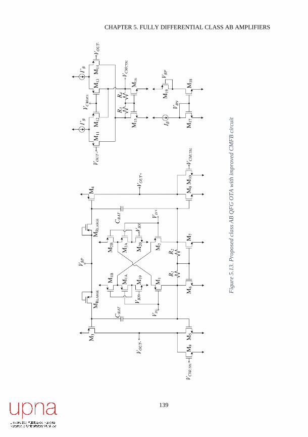
CHAPTER 5. FULLY DIFFERENTIAL CLASS AB AMPLIFIERS
139
Fig
ure
5.1
3. P
ropo
sed
cla
ss A
B Q
FG
OT
A w
ith i
mp
rove
d C
MF
B c
ircu
it

CHAPTER 5. FULLY DIFFERENTIAL CLASS AB AMPLIFIERS
140
The three OTAs in Figure 5.12(a), Figure 5.12(b) and Figure 5.13 have
been simulated using the same 0.5 μm CMOS technology employed previously.
The transistor sizes employed are shown in Table 5.3. Capacitors CBAT have a
value of 1 pF.
Transistor W/L (μm/μm)
M1-M2 50/0.6
M1A-M1B 50/0.6
M2A-M2B 240/0.6
M3-M4 180/0.6
M5-M10 60/0.6
M11-M14 50/0.6
M15-M16 60/0.6
MR1-MR2 1.5/0.6
Table 5.3. Transistors size of the Super Class AB QFG OTA
A dual supply voltage of 1 V was applied, and the bias current IB was
10 A. The bias current of CMFB circuit, IB’, was 10 A too. This current could
be smaller to decrease the power consumption. The OTAs were connected in
unity gain negative feedback shown in Figure 5.7 for time-domain simulations.
Figure 5.14. Simulated transient response of the OTAs
The input signal was a 1 MHz 0.5 V square wave with a -0.5 V
common-mode voltage. The resistor R shown in Figure 5.7 had a nominal value
of 100 kΩ. A high load capacitance of 70 pF is used to demonstrate the high
current driving capability of the proposed OTA. The simulated output of the

CHAPTER 5. FULLY DIFFERENTIAL CLASS AB AMPLIFIERS
141
OTAs is plotted in Figure 5.14. Note the stable and faster settling of the class
AB QFG OTA proposed.
Figure 5.15. Simulated open-loop frequency response of the OTAs
Figure 5.15 shows the simulated open-loop magnitude response of the
OTAs. The DC gain increases by 16.5 dB versus the class A OTA of
Figure 5.12(a) and almost 1 dB compared to the class AB OTA shown in
Figure 5.12(b). Concerning the increase in GBW, it is approximately a factor 16
due to the improved transconductance provided by the use of QFG transistors
and the enhaced bandwidth of the proposed CMFB scheme provides.
Table 5.5 indicates relevant performance parameters of the OTAs. The
slew rate is increased approximately 86 times for the same quiescent current and
load capacitance. The settling time in the proposed OTA is 36 ns, while the
classic class A OTA cannot settle for this input signal and load. Simulated THD
is <1% for a 0.9 Vpp input sinusoid, whereas the conventional class A OTA
shows THD>2% due to settling limitations.. The dynamic range of the proposed
OTA is higher than for class A and class AB OTAs, despite of integrating its
equivalent input noise density in a greater frequency band (corresponding to
their GBW product). However, static power increases a 20% by the extra bias
current required. This issue can be solved if a smaller bias current of CMFB
circuit, IB’, is used. Another drawback is that the silicon area is higher due to the
floating capacitors CBAT and the resistors used in the LCMFB technique.
A test chip was fabricated using the same 0.5 μm CMOS technology,
and containing the circuit of Figure 5.13 connected following the topology of
Figure 5.7. Resistors R were fabricated on chip, while capacitors CL were
external. A photograph of the fabricated OTA is shown inside the white box of

CHAPTER 5. FULLY DIFFERENTIAL CLASS AB AMPLIFIERS
142
Figure 5.16. The silicon area employed for the circuit is approximately
0.045 mm2.
Figure 5.16. Microphotograph of the proposed super class AB QFG OTA
The measured response of the proposed OTA to a 100 kHz 0.5 V square
input waveform is plotted in Figure 5.17. Bias current IB was 30 A. A load
capacitance of 47 pF was employed, which is increased to about 70 pF by the
pad, board and test probe parasitic capacitances. Measured positive and negative
SR values are 11.8 V/s and -11.2 V/s respectively, and the measured settling
time is 60 ns. The measured THD for an input tone of 100 kHz and 0.9 Vpp is
-53.44 dB.
Figure 5.17. Experimental transient response of the proposed OTA
Therefore, thanks to diverse adaptive biasing techniques, an improved
class AB QFG OTA has been proposed. This amplifier has a simple and compact
implementation and does not require extra supply voltage. It also improves slew
rate and settling significantly without increasing quiescent power. This circuit
can be applied in micropower switched capacitor systems and in voltage
followers requiring to drive large capacitive loads.

CHAPTER 5. FULLY DIFFERENTIAL CLASS AB AMPLIFIERS
143
5.4 Class AB OTA with improved current follower
In Chapter 2, several cascode topologies have been proposed, which
are very useful to improve the gain of the amplifier without adding extra gain
stages, thus complicating stability and increasing power consumption. However,
the signal swing available at the output is limited by the input transistors. This
issue can be solved by avoiding to place the input transistors at the output
branch. An efficient way of achieving that is the use of a current follower CF
(or current amplifier CA if current gain K is provided) which conveys (and
scales for K1) the signal current generated at the differential pair to the output
branch, just as it was done in Section 5.3. Figure 5.18(a) shows the conceptual
scheme. The CF/CA presents low impedance input (ideally a signal ground) in
order to sense the input current without adding low-frequency poles or zeros,
and also high- impedance output to achieve large amplifier gain.
Figure 5.18. (a) Conventional single-stage class A amplifier
(b) Proposed single-stage class AB amplifier
Figure 5.19(a) and Figure 5.19(b) show two common implementations
of these blocks, using current mirrors and common-gate amplifiers, respectively.
The common-mode feedback (CMFB) circuit is not shown for simplicity. When
they are applied to the circuit of Figure 5.18(a), the conventional current mirror
(CM) amplifier and folded cascode (FC) amplifier result. The CM and FC
amplifiers not only keep the gain and bandwidth of the telescopic cascode
amplifier but also improve the output range. Note that in these arrangements the
differential pair already provides an input bias current IB to the CF/CA, so the
bottom current sources in Figure 5.19(b) are 2IB.

CHAPTER 5. FULLY DIFFERENTIAL CLASS AB AMPLIFIERS
144
Figure 5.19. Differential CF implementation (a) with current mirrors
(b) with common-gate transistors
A disadvantage of the topology of Figure 5.18(a) is that it operates in
class A, limiting the output currents to the bias current 2IB. Hence, the power
consumption must be increased in order to improve the dynamic performance of
the amplifier. This can be solved by applying adaptive biasing techniques to the
differential pair. With this method, class AB operation is achieved, as low
quiescent currents can be used in the differential pair and at the same time large
dynamic currents not bounded by the quiescent currents are generated for large
input signals. As mentioned in previous sections, several class AB amplifiers
have been reported, using different adaptive biasing techniques [6]-[15].
However, the CF/CA is often unchanged, which may limit the dynamic
performance of the amplifier. The objective of this section is to design such
CF/CA topologies in an optimal way to achieve class AB amplifiers. Besides, a
novel class AB amplifier is presented as an application example.
Figure 5.19(a) shows two current mirrors, which is the most commonly
used configuration for achieving a current follower or a current. They are
frequently employed in OTAs, linear transconductors, CFOAs, current
conveyors and several current-mode circuits. The main benefits of the current
mirror are its simplicity and the possibility to scale the output current by the
current mirror ratio K, thus improving the gain-bandwidth product (GBW) of
the amplifier by the same scale factor K. However, there are also disadvantages
using current mirrors. The main ones are:
a) The current mirror introduces a pole ωp ≈ -gm1B/(Cgs1A+Cgs1B) and a zero
ωz ≈ -(1+K)·ωp, which may limit high-frequency performance, mainly for
large K ratios since they increase parasitic capacitance Cgs1B. This fact limits
the maximum K value used in practice.
CHAPTER 5. FULLY DIFFERENTIAL CLASS AB AMPLIFIERS
145
b) Increasing K also rises quiescent power consumption since K applies both
to the quiescent current and the signal current.
c) Accuracy of the current mirror relies on perfect matching between the
current mirror transistors, which is not possible in practice due to geometric
and parametric variations.
The current follower of Figure 5.19(b) does not have any matching
requirement between devices. The output current is exactly the inverted input
current as long as the bias current sources in Figure 5.19(b) remain
signal-independent. Moreover, the additional pole introduced is ωp ≈ -gm1/Cgs1,
which is in general at higher frequency than that of Figure 5.19(a) for the same
transistor dimensions and bias current, due to the lower intrinsic capacitance at
the input. However, this CF cannot scale the output current, so it does not
contribute to increasing the transconductance (and hence the GBW) of the
amplifier.
A shortcoming of both circuits in Figure 5.19 is that the maximum
signal current is limited by the bias current IB. For the NMOS topology in
Figure 5.19(a) the maximum current leaving the current mirror is IB (a PMOS
current mirror would lead to the same limitation for the current entering the
mirror). In the current follower of Figure 5.19(b), the maximum signal current
entering the circuit is IB. In the next paragraphs, a modification is employed to
overcome this limitation, yielding a class AB topology.
The proposed single-stage class AB amplifier corresponds to the
topology shown in Figure 5.18(b). There are several choices for the adaptive
biasing of the differential pair, as it was explained in Section 2.2.3.1 [6]. In this
design, the cross-coupled DC level shifters option has been used, doubling the
transconductance.
The differential CF/CA employed is shown in Figure 5.20. It is based
on the differential high-swing current mirror implementation of Figure 5.19(a),
including two modifications. First, the input current is sensed at the source of
MCN1-MCN2, in order to benefit from the reduced input resistance at this node
due to the FVF feedback loop. Second, the quasi-floating gate (QFG) technique
[18] is applied to achieve class AB operation. It is based on including two
capacitors CBAT and two high-resistance pseudo-resistors MPR. In quiescent

CHAPTER 5. FULLY DIFFERENTIAL CLASS AB AMPLIFIERS
146
operation these new devices have no effect since capacitors act as open circuits
and there is no current flowing through transistors MPR. However, when a
positive differential input current IINd=IIN+-IIN- appears, voltage at node A
increases and voltage at node B decreases. Due to the large value of the
equivalent resistance Rlarge of the pseudo resistors MPR, capacitors CBAT cannot
discharge rapidly so that they behave as floating batteries, transferring voltage
variations from nodes A and B to nodes C and D, respectively. The increased
voltage at node C reduces the current flowing through transistors MP1-MP2 at the
right-hand side, and the decreased voltage at node D boosts the current flowing
through transistors MP1-MP2 at the left-hand side above IB When a negative
differential input current IINd=IIN+-IIN- appears, now voltage at node A decreases
and voltage at node B increases, yielding a decrease at node C and an increase
at node D. Hence the opposite situation happens at the output terminals.
Consequently, positive and negative input currents much larger than IB can be
applied to either input terminal without compromising dynamic performance.
Figure 5.20. Class AB differential CF/CA using QFG techniques
The capacitive divider formed by CBAT and the intrinsic capacitance CP
at the gate of MP1-MP2 leads to attenuation in the voltage transfer from nodes A
to C (and B to D) given by the expression α = CBAT/(CBAT+CP). Moreover, the
signal transferred to these nodes is also high-pass filtered by the first order RC
filter formed by CBAT and MPR, with cutoff frequency
f-3dB=1/[2πRlarge(CBAT+CP)]. Due to the extremely large value of Rlarge and the
typically low value of CP, a f-3dB<1 Hz and α>0.75 can be achieved with
CBAT ≈ 1 pF. Hence in practice all the AC components of voltage at nodes A and
B can be transferred to nodes C and D with low attenuation, with a modest
increase in silicon area (about 1000 μm2 more in the process employed).

CHAPTER 5. FULLY DIFFERENTIAL CLASS AB AMPLIFIERS
147
The detailed circuit of the proposed class AB OTA of Figure 5.18(b)
using the adaptive biasing mentioned and the CF/CA of Figure 5.20 is shown in
Figure 5.21(a). A conventional CMFB circuit, based on a differential difference
amplifier was used. It is shown in Figure 5.22.
Figure 5.21. (a) Proposed class AB amplifier (b) Class A amplifier used for comparison
As for the small-signal parameters, the transconductance of the
proposed amplifier is
𝐺𝑚𝐴𝐵 = 2𝐾𝑔𝑚1 (5.15)
with K the current gain factor of the circuit in Figure 5.20, given by
K=(W/L)MN2/(W/L)MN1=(W/L)MP2/(W/L)MP1. The output resistance of the
amplifier is
𝑅𝑜𝐴𝐵 ≈ 𝑔𝑚𝐶𝑃2𝑟𝑜𝐶𝑃2(𝑟𝑜𝑃2‖𝑟𝑜𝑃4)‖𝑔𝑚𝐶𝑁2𝑟𝑜𝐶𝑁2(𝑟𝑜𝑁2‖𝑟𝑜𝑁3) (5.16)
and the DC gain is ADC = GmAB·RoAB. The GBW is given by
𝐺𝐵𝑊𝐴𝐵 =𝐾𝑔𝑚1
𝜋𝐶𝐿 (5.17)

CHAPTER 5. FULLY DIFFERENTIAL CLASS AB AMPLIFIERS
148
Figure 5.22. Common-mode feedback circuit
Besides small-signal analysis, an approximate expression for slew rate
(SR) can be obtained by using the simple square law model for the MOS
transistor in strong inversion and saturation. For a large positive differential
input voltage Vid=Vin+-Vin-, current in transistor M1 is
𝐼1 =𝛽1
2(√
2𝐼𝐵𝐼𝐴𝑆
𝛽4+ 𝑉𝑖𝑑)
2
(5.18)
whereas current I2 can be neglected. This large current is conveyed to the output
by the circuit of Figure 5.20. Hence for a differential input step of A Volts, the
SR+ is
𝑆𝑅𝐴𝐵+ =𝐾𝛽1
2𝐶𝐿(√
2𝐼𝐵𝐼𝐴𝑆
𝛽4+ 𝐴)
2
(5.19)
Analogously, for a large negative differential input step of amplitude
A, the SR- is
𝑆𝑅𝐴𝐵− =𝐾𝛽2
2𝐶𝐿(√
2𝐼𝐵𝐼𝐴𝑆
𝛽3+ 𝐴)
2
(5.20)
In practice SR values are lower due to second-order effects not
considered in the simple MOS square law model, and because some transistors
can leave saturation for large transients.
Note that the SR for the class A version of Figure 5.21(b) using the
same bias current is
𝑆𝑅𝐴+ = 𝑆𝑅𝐴− =2𝐾𝐼𝐵𝐼𝐴𝑆
𝐶𝐿 (5.21)

CHAPTER 5. FULLY DIFFERENTIAL CLASS AB AMPLIFIERS
149
Considering thermal noise and assuming that all transistors operate in
strong inversion and saturation, the equivalent input noise of the proposed
amplifier is
𝑣𝑛,𝑖𝑛𝐴𝐵2 =
4𝑘𝐵𝑇∆𝑓
3𝑔𝑚12 × (𝑔𝑚1 + 𝑔𝑚4 + 𝑔𝑚𝑁1 + 𝑔𝑚𝑃1 +
𝑔𝑚𝑃2+𝑔𝑚𝑃4+𝑔𝑚𝑁2+𝑔𝑚𝑁3+𝑔𝑀𝑛4
𝐾2)(5.22)
Note that as expected the influence of the output branch transistors
decreases for larger K when referred to the input. The CMFB circuit does not
influence noise as its noise is cancelled by the differential output arrangement.
The class A and class AB amplifiers of Figure 5.21 were simulated
using a 0.5 μm CMOS n-well process. A class A CF/CA (the circuit of
Figure 5.20 but without capacitors CBAT and pseudo-resistors MPR) is used in the
circuit of Figure 5.18 . The transistor sizes employed are shown in Table 5.4.
Capacitors CBAT have a value of 1 pF. Supply voltages were ±1 V, and bias
currents IB and IBIAS were set to 10 μA. Cascode bias voltages VCP and VCN were
set to -0.3 V and 0.2 V, respectively. Load capacitance was CL = 25 pF.
Transistor W/L (m/m)
M1, M2, M3, M4 100/1
M5, M6 100/0.6
MN1, MN2 60/1
MCN1, MCN2 60/0.6
MP1, MP2, MP3, MP4 100/0.6
MP5, MP6, MP7, MP8 200/0.6
MCP1, MCP2, MCP3 200/0.6
MN3, MN4, MN5, MCN4, MCN5 100/3
MPR 1.5/1
Table 5.4. Transistor Aspect Ratio of amplifiers of Figure 5.21
Figure 5.23 shows the simulated open loop AC small signal response
of both amplifiers of Figure 5.21. The DC gain of the class A and class AB
amplifiers is 54.9 dB and 61.5 dB respectively. This improvement is mainly due
to the extra 6 dB provided by the adaptive biasing topology. The GBW of the
class A and class AB amplifiers is 1.07 MHz and 2.31 MHz, respectively. Note
the increase in GBW by a factor >2. The phase margin of the class A and class
AB amplifiers is 89.3º and 87º, respectively. At 2.31 MHz the phase margin of

CHAPTER 5. FULLY DIFFERENTIAL CLASS AB AMPLIFIERS
150
the class A amplifier is 88º, hence a degradation of just 1º is observed for the
class AB version.
Figure 5.23. Simulated open-loop frequency response of amplifiers of Figure 5.18
The transient response of the amplifiers of Figure 5.21 were simulated
connecting them in unity gain configuration using passive feedback resistors of
R=100 kΩ, as shown in Figure 5.7, and the same CL = 25 pF. A 100 kHz 0.4 V
differential input square with -0.3 V common-mode voltage was applied to the
input. Figure 5.24 shows the simulated output of the amplifiers. Note the stable
and faster settling of the proposed class AB amplifier. The SR of the class A
amplifier is 0.62 V/μs, while the SR of the proposed class AB amplifier is 2.7
V/μs, i.e., >4 times higher for the same quiescent current and load capacitance.
Figure 5.25 shows the simulated Total Harmonic Distortion (THD)
using a 100 kHz differential input tone of different amplitude. Note the
improved linearity of the proposed amplifier, due to the enhanced dynamic
performance.

CHAPTER 5. FULLY DIFFERENTIAL CLASS AB AMPLIFIERS
151
Figure 5.24. Simulated transient response of amplifiers of Figure 5.21
Figure 5.25. Simulated THD vs input amplitude at 100 kHz
The class AB amplifier of Figure 5.21(a) in the arrangement shown in
Figure 5.7 was fabricated in the same 0.5 μm CMOS technology used for the
simulations. On-chip resistors R were made by a high resistance polysilicon
layer available in the technology. The outputs were directly connected to
bonding pads. As no load capacitors were used off-chip, load capacitance in the
measurements corresponds to the pad, board and test probe capacitance. Its
estimated value is 25 pF. Figure 5.26 shows a microphotograph of the class AB
amplifier, enclosed by the white rectangle. The silicon area employed is
500 μm 150 μm. Supply voltage as well as bias currents/voltages employed
for the measurements were the same as for the simulations.

CHAPTER 5. FULLY DIFFERENTIAL CLASS AB AMPLIFIERS
152
Figure 5.26. Microphotograph of amplifier in Figure 5.21(a)
Figure 5.27 shows the measured response to a 0.4 V 100 kHz periodic
input square waveform. The measured SR is 3.4 V/μs, in close agreement with
the simulation results.
Figure 5.27. Measured transient response of amplifier in Figure 5.21(a)
Table 5.5 summarizes the main simulation and measurement results of
the amplifier and other reported class AB amplifiers. The main drawback of the
proposed amplifier is a small area increase due to the capacitors CBAT and the
adaptive biasing.
Hence, the combination of a power efficient adaptive biasing circuit
and a class AB current follower able to handle the large dynamic currents
generated is the main idea of the proposed amplifier. Simulation and
measurement results confirm the advantages of this approach.

CHAPTER 5. FULLY DIFFERENTIAL CLASS AB AMPLIFIERS
153
5.5 Differential class AB recycling folded cascode
In Chapter 4, several single-ended Recycling Folded Cascode
topologies were proposed with good features. However, due to the multiple
benefits of fully differential topologies previously explained in the introduction
of this Chapter, even better performance can be obtained.
A fully differential (FD) version of the OTA of Figure 4.17 can be
simply obtained by replacing the output current mirror by two matched current
sources and including a Common-Mode Feedback (CMFB) circuit, as shown in
Figure 5.28(a). The analysis performed for the single ended super class AB RFC
OTA in Section 4.1.3 essentially applies to this FD implementation. However,
as for the FD RFC OTA, there is a potential asymmetry in the charge/discharge
rate of the outputs that can be balanced by a fast and accurate CMFB [14].
An alternative FD implementation is shown in Figure 5.28(b) based on
[17]. The gates of M9 and M10 are connected to the gates of M2D and M1D,
respectively. Hence current in M1D and M2D is copied to the output branches,
increasing the Gm and therefore the DC gain and GBW of the OTA.
Both the conventional (replacing the output PMOS current mirror by
two matched current sources) and proposed fully differential implementation of
the super class AB RFC OTA, shown in Figure 5.28, were simulated using a 0.5
m CMOS technology. Time-domain simulations were done in closed-loop
configuration. The same component dimensions, supply voltage and bias
currents as for the single-ended versions were employed, that is, those in
Table 4.4. The CFMB circuit of Figure 5.2(c) controlling NMOS current sources
was used in both OTAs to get a fast CMFB loop. Table 5.5 summarizes the main
results, evidencing the improvement of the OTA of Figure 5.28(b).

CHAPTER 5. FULLY DIFFERENTIAL CLASS AB AMPLIFIERS
154
(a)
(b)
Figure 5.28. FD super class AB RFC OTA (a) Conventional (b) Proposed
Therefore, with the simple modification done in Figure 5.28(b), better
performance is obtained: better linearity, greater GBW and DC gain (thus less
input-referred noise) when comparing with Figure 5.28(a).

CHAPTER 5. FULLY DIFFERENTIAL CLASS AB AMPLIFIERS
155
5.6 Comparison of the differential amplifiers
As in Chapter 4, a final Section is included in order to compare the
amplifiers proposed in this Chapter, and also with other previously published
ones.
Table 5.5 contains the most important parameters of every considered
amplifier. Among the proposed ones, the OTA Figure 5.13 presents the highest
Slew Rate value (18.1 V/s). Its THD is also the lowest (since that of
Figure 5.28(b) was calculated by simulation and with a lower amplitude). As for
the small signal parameters, Figure 5.28(b) has the highest DC gain and GBW.
It is worth mentioning that some of the equivalent input noise values
were obtained by simulation, thus those values are lower than the experimental
ones.
To simplify the comparison of all the amplifiers, Figure 5.29 is
provided. OTAs of Figure 5.13, Figure 5.28(a) and Figure 5.28(b) present the
best FoMs in both small and large signal domains, even if compared with other
previously published amplifiers which were fabricated in newer technologies.
Thus, it can be said that the fully-differential amplifiers proposed in
this chapter obtain very good performance despite their low power consumption,
i.e, they are power-efficient solutions.

CHAPTER 5. FULLY DIFFERENTIAL CLASS AB AMPLIFIERS
156
FoM
S
116
.7
205
.6
25.6
137
.1
350
48.1
300
410
FoM
L
0.8
4
5.5
1
0.1
5
4.4
9
10.5
6
0.7
1
9
9.5
Are
a
(mm
2)
0.0
11
0.0
13
0.0
24
0.0
40
0.0
45
0.0
75
--
--
Po
wer
(μW)
120
160
200
240
240
240
140
140
Eq.
inp
ut
no
ise
@1M
Hz
(nV
/H
z)
86
84
35.8
*
13.3
*
12.4
*
93
15*
14*
GB
W
(MH
z)
1
2.3
5
0.3
66
2.3
5
6
2.3
1
3
4.1
PM
*
(º)
90
89.8
94
88.9
80.5
87
76
74
AD
C*
(dB
)
30.8
36.7
20.8
36.4
37.3
61.5
74.6
76
TH
D (
dB
)
-34
.1
@100
kH
z
0.6
Vpp
-53
.9
@100
kH
z
0.6
Vpp
-31
.6
@100
kH
z
0.9
Vpp
-54
.5
@100
kH
z
0.9
Vpp
-71
.7
@100
kH
z
0.9
Vpp
-47
@100
kH
z
0.5
Vpp
-63
@100
kH
z
0.5
Vpp
-72
@100
kH
z
0.5
Vpp
SR
-
(V/μs)
-0.8
5
-6.4
-0.2
1
-7.6
-16
.6
-9
-10
SR
+
(V/μs)
0.7
2
6.3
0.2
1
7.7
18.1
3.4
9
9
CL
(pF
)
70
70
70
70
70
25
70
70
CM
OS
tech
.
(μm)
0.5
0.5
0.5
0.5
0.5
0.5
0.5
0.5
Fig
ure
5.9
(a)
Fig
ure
5.9
(b)
Fig
ure
5.1
2(a
)
Fig
ure
5.1
2(b
)
Fig
ure
5.1
3
Fig
ure
5.2
1(a
)
Fig
ure
5.2
8(a
)*
Fig
ure
5.2
8(b
)*

CHAPTER 5. FULLY DIFFERENTIAL CLASS AB AMPLIFIERS
157
F
oM
S
210
30.4
22.7
88.9
70
165
.4
261
.7
FoM
L
1.1
7
0.7
5
0.2
6
0.1
9
0.3
9
0.9
9
2.2
4
Are
a
(mm
2)
0.0
12
0.0
57
0.0
26
0.1
57
0.0
29
0.0
20
0.0
70
Po
wer
(μW)
110
1.2
110
197
437
.5
25.4
1190
0
Eq.
inp
ut
no
ise
@1M
Hz
(nV
/H
z)
14.1
--
80
<60
--
100
--
GB
W
(MH
z)
35
0.0
57
2.5
11.6
7
4.9
3
86.5
PM
*
(º)
>45
60
--
66.1
83
60
50
AD
C*
(dB
)
>70
51
52
88.3
63.4
57.5
72
TH
D (
dB
)
--
-52
@ 1
kH
z
0.5
Vpp
-40
@0
.4 V
pp
--
-47
.1
@ 2
Vpp
-40
.1
@250
kH
z
0.4
Vpp
--
SR
-
(V/μs)
--
--
--
-1.3
7
-3.3
-3.8
--
SR
+
(V/μs)
19.5
0.1
4
2.8
9
2.5
3
2.7
1.8
74.1
CL
(pF
)
>5
.5
8
20
15
25
20
200
CM
OS
pro
cess
(μm)
0.1
3
0.1
8
0.1
8
0.3
5
0.5
0.1
8
0.1
8
[9]
[10
]
[11
]
[12
]
[13
]
[14
]
[15
]
*S
imu
lati
on
T
ab
le 5
.5. S
um
ma
ry o
f m
easu
rem
ent
resu
lts
an
d p
erfo
rman
ce c
om
pa
riso
n

CHAPTER 5. FULLY DIFFERENTIAL CLASS AB AMPLIFIERS
158
Figure 5.29. Comparative chart considering a small-signal and a large-signal FoMs
5.7 Conclusions
Chapter 5 proposes novel low-voltage class AB fully differential
amplifiers, due to their several benefits versus single-ended topologies.
Different techniques have been applied in order to develop these blocks whose
performance has been improved compared with conventional circuits. In
addition, an enhanced CMFB circuit has been proposed.

CHAPTER 5. FULLY DIFFERENTIAL CLASS AB AMPLIFIERS
159
Bibliography of the Chapter
[1] J. F. Duque-Carrillo, “Control of the common-mode component in
CMOS continuous-time fully differential signal processing”, Analog
Integrated Circuits and Signal Processing, vol. 4, no. 2, pp. 131-140,
1993.
[2] E. Säckinger and W. Guggenbühl, “A versatile bulding block: the
CMOS differential difference amplifier”, IEEE Journal of Solid-State
Circuits, vol. 22, no. 2, pp. 287-294, 1987.
[3] L. Lah, J. Choma and J. Draper, “A continuous-time common-mode
feedback circuit (CMFB) for high-impedance current-mode
applications”, IEEE Transactions on Circuits and Systems II, vol. 47,
no. 4, pp. 363-369, Apr. 2000.
[4] J. Wang, S. Bu, Z. Fu, D. Li and K. P. Pun, “An efficient frequency
compensation scheme for CMFB loop in fully differential amplifiers”,
2015 IEEE International Conference on Electron Devices and
Solid-State Circuits (EDSSC), pp. 415-418, 2015.
[5] J. Ramirez-Angulo and M. Holmes, “Simple technique using local
CMFB to enhance slew rate and bandwidth of one-stage CMOS
op-amps”, Electronics Letters, vol. 38, no. 23, pp. 1409-1411, 2002.
[6] A. Lopez-Martin, S. Baswa, J. Ramírez-Angulo and R. G. Carvajal,
“Low-voltage super class AB CMOS OTA cells with very high slew
rate and power efficiency”, IEEE Journal of Solid-State Circuits,
vol. 40, no. 5, pp. 1068-1077, May 2005.
[7] S. Baswa, A. Lopez-Martin, J. Ramirez-Angulo and R. G. Carvajal,
“Low-voltage micropower super class AB CMOS OTA”, Electronics
Letters, vol. 40, no. 4, pp. 216-217, 2004.
[8] J. Ramirez-Angulo, R.G. Carvajal, J. A. Galan and A. Lopez-Martin,
“A free but efficient low-voltage class-AB two-stage operational
amplifier,” IEEE Transactions on Circuits and Systems II: Express
Briefs, vol. 53, no. 7, pp. 568-571, 2006.

CHAPTER 5. FULLY DIFFERENTIAL CLASS AB AMPLIFIERS
160
[9] M. Figueiredo, R. Santos-Tavares, E. Santin, J. Ferreira, G. Evans and
J. Goes, “A two-stage fully differential inverter-based self-biased
CMOS amplifier with high efficiency”, IEEE Transactions on Circuits
and Systems I: Regular Papers, vol. 58, no. 7, pp. 1591-1603, 2011.
[10] M. R. Valero Bernal, S. Celma, N. Medrano and B. Calvo, “An
ultralow-power low-voltage class-AB fully differential opamp for
long-life autonomous portable equipment”, IEEE Transactions on
Circuits and Systems II: Express Briefs, vol. 59, no. 10, pp. 643-647,
2012.
[11] S. Chatterje, Y. Tsividis and P. Kinget, “A 0.5-V bulk-input fully
differential operational transconductance amplifier”, Proceedings of
the 30th European Solid-State Circuits Conference (ESSCIRC),
pp. 147-150, Leuven, Belgium, 2004.
[12] L. Zuo and S. K. Islam, “Low-voltage bulk-driven operational
amplifier with improved transconductance”, IEEE Transactions on
Circuits and Systems I: Regular Papers, vol. 60, no. 8, pp. 2084-2091,
2013.
[13] P. R. Surkanti and P. M. Furth, “Converting a three-stage
pseudoclass-AB amplifier to a true-class-AB amplifier,” IEEE
Transactions on Circuits and Systems II: Express Briefs, vol. 59, no. 4,
pp. 229-233, 2012.
[14] E. Cabrera-Bernal, S. Pennisi, A. D. Grasso, A. Torralba and R. G.
Carvajal, “0.7-V three-stage class-AB CMOS Operational
Transconductance Amplifier”, IEEE Transactions on Circuits and
Systems I: Regular Papers, vol. 63, no. 11, pp. 1807-1815, 2016.
[15] S. Sutula, M. Dei, L. Teres and F. Serra-Graells, “Variable-mirror
amplifier: a new family of process-independent class-AB single-stage
OTAs for low-power SC circuits”, IEEE Transactions on Circuits and
Systems I: Regular Papers, vol. 63, no. 8, pp. 1101-1110, 2016.
[16] R. G. Carvajal, J. Ramirez-Angulo, A. J. Lopez-Martin, A. Torralba,
J. A. Galan, A. Carlosena and F. M. Chavero, “The Flipped Voltage
Follower: a useful cell for low-voltage low-power circuit design”,
IEEE Transactions on Circuits and Systems I, vol. 52, no. 7,
pp.1276-1291, 2005.

CHAPTER 5. FULLY DIFFERENTIAL CLASS AB AMPLIFIERS
161
[17] V. Peluso, P. Vancorenland, M. Steyaert and W. Sansen, “900mV
differential class AB OTA for switched opamp applications”,
Electronics Letters, vol. 33, no. 17, pp. 1455-1456, 1997.
[18] J. Ramirez-Angulo, A.J. López-Martín, R.G. Carvajal and
F. Muñoz-Chavero, “Very low voltage analog signal processing based
on Quasi Floating Gate transistors”, IEEE Journal of Solid-State
Circuits, vol. 39, no. 3, pp. 434-442, 2003.
[19] R. Assaad and J. Silva-Martinez, “The recycling folded cascode: a
general enhancement of the folded-cascode amplifier”, IEEE Journal
of Solid-State Circuits, vol. 44, no. 9, pp. 2535-2542, 2009.

CHAPTER 5. FULLY DIFFERENTIAL CLASS AB AMPLIFIERS
162
163
Chapter 6
APPLICATIONS OF CLASS AB
AMPLIFIERS
In Section 2.2.1, a low voltage technique was presented, based on
choosing a more convenient DC operating point for the input transistors,
achieving rail-to-rail operation. This technique can be applied to different
systems, since the opamp is a very versatile analog building block.
In this Chapter, three different applications of the same technique are
described. A low voltage buffer is proposed in Section 6.1. Section 6.2 describes
a Sample and Hold. In Section 6.3, a Delta-Sigma modulator is presented, also
capable of operating in low-voltage conditions. Finally, conclusions are given
in Section 6.4.
Since two of these applications are related to Analog-to-Digital
conversion, the main basic concepts of this process are introduced in
Appendix D.
6.1 Low Voltage Buffer
In Chapter 2, different approaches have been presented in order to design
low-voltage low-power amplifiers. However, there are more possible
implementations. In [1], the concept of switched op-amps was proposed, which

CHAPTER 6. APPLICATIONS OF CLASS AB AMPLIFIERS
164
made use of switched capacitors to achieve low-voltage op-amps. Based on this
theory, in [2] the circuit shown in Figure 6.1 is proposed.
Figure 6.1. Switched op-amp buffer [2]
As it can be seen from the figure above, this amplifier is connected in
inverting configuration. During phase ϕ1, capacitor C2 is charged to VDD-VSS,
while charge in C1 is null, as its terminals are connected to VSS. However, in
phase ϕ2, both capacitors share their charge. As the positive input terminal of the
amplifier is set to VDD, the negative terminal is forced to the same voltage, thus
voltage at node X is 0 V, which is the same voltage as the input common-mode
voltage, permitting the amplifier to work in low-voltage operation.
The main drawback of this topology is that it only works in ϕ2, as the
output terminal is VDD in ϕ1. To solve this issue, the following circuit is
proposed.
Figure 6.2. Proposed low-voltage amplifier
The proposed topology works as follows. In phase 1, C2 is charged to
VDDP. (a voltage slightly lower than VDD). Supposing C1 is initially discharged,
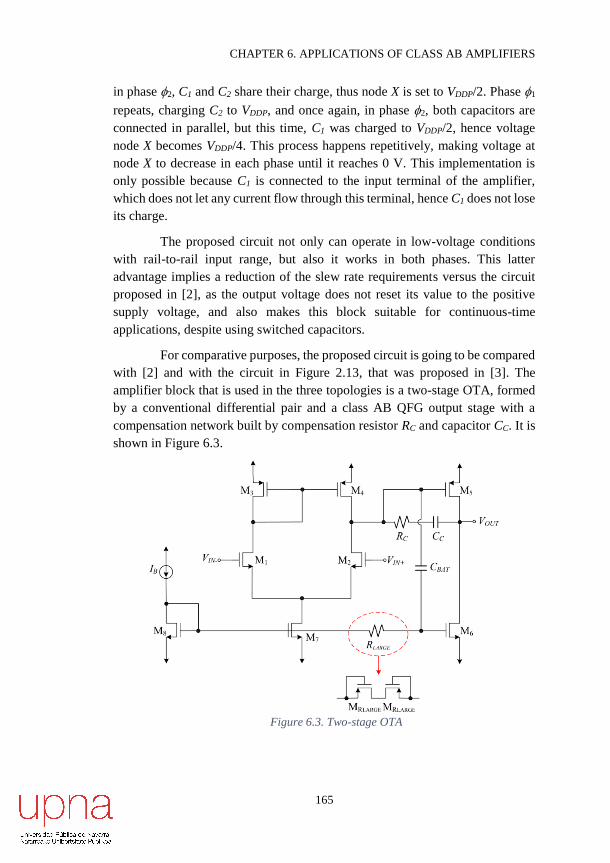
CHAPTER 6. APPLICATIONS OF CLASS AB AMPLIFIERS
165
in phase 2, C1 and C2 share their charge, thus node X is set to VDDP/2. Phase 1
repeats, charging C2 to VDDP, and once again, in phase 2, both capacitors are
connected in parallel, but this time, C1 was charged to VDDP/2, hence voltage
node X becomes VDDP/4. This process happens repetitively, making voltage at
node X to decrease in each phase until it reaches 0 V. This implementation is
only possible because C1 is connected to the input terminal of the amplifier,
which does not let any current flow through this terminal, hence C1 does not lose
its charge.
The proposed circuit not only can operate in low-voltage conditions
with rail-to-rail input range, but also it works in both phases. This latter
advantage implies a reduction of the slew rate requirements versus the circuit
proposed in [2], as the output voltage does not reset its value to the positive
supply voltage, and also makes this block suitable for continuous-time
applications, despite using switched capacitors.
For comparative purposes, the proposed circuit is going to be compared
with [2] and with the circuit in Figure 2.13, that was proposed in [3]. The
amplifier block that is used in the three topologies is a two-stage OTA, formed
by a conventional differential pair and a class AB QFG output stage with a
compensation network built by compensation resistor RC and capacitor CC. It is
shown in Figure 6.3.
Figure 6.3. Two-stage OTA

CHAPTER 6. APPLICATIONS OF CLASS AB AMPLIFIERS
166
Figure 6.4. Low-Voltage Amplifiers (a) [2] (b) [3]
(c) Proposed switched-capacitors approach

CHAPTER 6. APPLICATIONS OF CLASS AB AMPLIFIERS
167
The three blocks that are going to be compared are displayed in
Figure 6.4. Note that the circuit in Figure 6.4(b) is using the additional block in
Figure 2.14 to create VCNTP and VCNTN. Switches have been implemented by
transistors. PMOS transistors are employed when switches are connected to a
voltage close to VDD. In any other case, NMOS transistors are used. Clock
signals are generated by a conventional scheme of non-overlapping clock
generator, shown in Figure 6.5. Note the use of Cgap to increase the gap between
the pulses. In the proposed topology, NMOS transistors implementing switches
are controlled by boosted clocks, obtained from a clock doubler (which was
depicted in Figure 3.11), to ensure they are totally open or close, since we are
operating with voltages near their threshold voltage.
Figure 6.5. Non-overlapping clock generator block
Circuits in Figure 6.4 have been simulated with Cadence, using a
0.13 m CMOS technology. Positive and negative supply voltages are 0.3 V,
bias current IB is 10 A and cascode voltages VCP and VCN are -50 mV and
50 mV, respectively. Transistor sizes are shown in Table 6.1. The value of
resistors R1 and R2 that form the inverting stage is 100 k, where resistors R3,
R4 and R5 has been set to 70 k, 210 k and 280 k, respectively. Resistor RBAT
is 210 k, as its value is the same as R4. These values have been chosen in order
to obtain VDDP = 225 mV. Capacitors C1 and C2 have a value of 2 pF and load
capacitors CL are 20 pF.

CHAPTER 6. APPLICATIONS OF CLASS AB AMPLIFIERS
168
Transistor W/L (μm/nm)
M1-M2 10/210
M3-M4 30/210
M5 60/210
M6-M8 20/210
M9-M10 10/210
M11-M12 30/210
M13-M14 20/210
M15-M18 60/210
M19-M24 20/210
MRlarge 0.3/160
Table 6.1. Transistors size of low voltage OTAs in Fig. 6.4
Figure 6.6. Simulated transient response of the three amplifiers
Figure 6.6 represents the transient response of the three amplifiers in
Figure 6.4. Frequency of the clock signal is 1 MHz. As input voltage, a 0.6 Vpp
50 kHz sinusoidal signal has been used. As figure below shows, the output of
Figure 6.4(a) should be VDD in one phase and follow the input in the following
phase. However, it requires high slew-rate, and circuit is slow when low supply
voltage is used. Figure 6.4(b) and Figure 6.4(c) obtain the same output signal,
verifying VOUT = -VIN. Nevertheless, the power consumption of the proposed
circuit is lower than that of Figure 6.4(b), 12 W vs 19.93 W. Note that the

CHAPTER 6. APPLICATIONS OF CLASS AB AMPLIFIERS
169
first cycles of the proposed circuit have some error, until X node reaches 0 V.
After that, it works correctly.
Besides of simulated results, experimental measurements were
obtained thanks to the prototype chip which was fabricated in the same 0.13 m
CMOS technology. It can be seen that the obtained results (shown in Figure 6.7)
are similar to that obtained by simulation, except for the circuit of Figure 6.4(a),
which works worse due to the higher experimental parasitic capacitance. In
addition, the amplifier proposed in [3] does not reach the maximum amplitude.
However, the proposed amplifier presents peaks caused by the switching
between both phases.
Figure 6.7. Measured transient response of the three amplifiers
Experimental THD measurements were also taken, obtaining -41.2 dB
for the amplifier of Figure 6.4(b) and -45.3 dB for the proposed one, when a
0.5 Vpp 50 kHz sinusoidal signal was applied to the input.
Thus, thanks to switched capacitors an efficient amplifier is achieved,
which is suitable for continuous-time applications.

CHAPTER 6. APPLICATIONS OF CLASS AB AMPLIFIERS
170
6.2 Sample & Hold
The Sample and Hold (S&H) circuit is a fundamental block of an ADC
circuit. It samples the input and holds this value for a certain time period. In its
simplest form it consists of a sampling switch and a holding capacitor. A
straightforward implementation of the switch is a transistor controlled by a clock
through its gate voltage. This topology is presented in Figure 6.8 [4].
Figure 6.8. Simplest Sample and Hold
However, in practice S&H implementations often include amplifiers to
improve accuracy. A conventional Sample and Hold circuit including an
amplifier is shown in Figure 6.9 [4].
Figure 6.9. Conventional Sample and Hold
Conventional S&H circuits operate in two non-overlapping clock
phases, 1 and 2. During 1, switches S1 and S2 are closed, whereas S3 remains
open. Thus, the input voltage is sampled in capacitor C and the output voltage

CHAPTER 6. APPLICATIONS OF CLASS AB AMPLIFIERS
171
is 0 V. During phase 2, S1 and S2 open, while S3 is closed, so the negative input
terminal has a voltage of 0 V thanks to the amplifier’s closed loop operation.
Fully differential topologies present some benefits over single-ended
schemes, as it was said in Chapter 5. Starting from the conventional Sample and
Hold circuit, the fully differential version can be constructed by duplicating the
capacitor and switches S1-3 in the positive input of the amplifier, and adding a
CMFB circuit. The main advantage of a fully differential Sample and Hold
circuit is that it does not require to reset the output to the input common-mode
voltage, thus relaxing the slew rate requirements of the amplifier. However, this
topology presents a limited input range. To avoid this problem, low voltage
techniques can be applied in order to extend the input range, allowing rail-to-
rail operation [5].
Figure 6.10 presents a proposed fully differential Sample and Hold.
Low-voltage techniques explained in Chapter 2 have been employed. As shown
in the figure below, besides the differential output terminals, the amplifier has
two additional outputs, VOUTaux+ and VOUTaux-, whose purpose is to maintain a
constant voltage VDDP at the input. A CMFB circuit ensures this fact. This way,
in phase 1, capacitors C store Vid-VDDP, and in phase 2, the differential output
voltage holds the value that Vid had at the end of phase 1. As the gate voltage
of the differential pair is VDDP, assuming NMOS amplifier input rail-to-rail
operation is achieved.
Figure 6.10. Proposed fully differential Sample and Hold

CHAPTER 6. APPLICATIONS OF CLASS AB AMPLIFIERS
172
The employed amplifier is shown in Figure 6.11. It has two output
stages, which are respectively used in each of the clock phases. In addition, the
active load of the differential amplifier has been rearranged by using a LCMFB
topology. The output stage that operates in phase 2 is class AB thanks to the
QFG technique. As it can be seen from Figure 6.11, there are two CMFB
circuits, one for the auxiliary output voltages, whose reference voltage is VDDP,
and the other one to adjust the output common-mode voltage to ground. Note
that every switch has been implemented as NMOS transistors, controlled by
non-overlapping boosted clocks (generated by circuits in Figure 3.11 and
Figure 6.5). Table 6.2 indicates the component parameters in Figure 6.10 and
Figure 6.11.
Component Value Component Value
M1-M2 40 μm / 210nm MRlarge 300 nm / 160 nm
M3-M4 75 μm / 210 nm MR 5 μm / 130 nm
M5-M8 150 μm / 210 nm MSW 500 nm / 130 nm
M9-M10 80 μm / 210 nm R 50 k
M11-M14 120 μm / 210 nm RVDD 15 k
M15-M16 40 μm / 210 nm RC1 1 k
M17-M20 75 μm / 210 nm RC2 5 k
M21-M22 80 μm / 210 nm C 1 pF
M23-M24 40 μm / 210 nm CC1 1 pF
M25-M28 75 μm / 210 nm CC2 4 pF
Table 6.2. Components' values of proposed S&H
Both the conventional S&H in Figure 6.9 (which employs the amplifier
in Figure 6.3) and the proposed S&H have been simulated in a 0.13 m CMOS
technology. Supply voltages were set to 0.3 V, and bias current IB is 10 A.
Auxiliary voltage VDDP is 200 mV. Two 20 pF grounded capacitors are
employed as load.

CHAPTER 6. APPLICATIONS OF CLASS AB AMPLIFIERS
173
Fig
ure
6.1
1. S
chem
ati
c o
f th
e p
rop
ose
d S
&H
am
pli
fier

CHAPTER 6. APPLICATIONS OF CLASS AB AMPLIFIERS
174
The simulated transient response of both S&H circuits to a 50 kHz
0.5 Vpp sinusoidal input signal (also shown in the same picture) is included in
Figure 6.12. The frequency of clocks is 1 MHz. Both S&H work properly but
the fully differential S&H does not need to reset the output to VCMIN, and it can
operate rail-to-rail. Although its static power consumption is higher than the
conventional topology, due to the inclusion of two CMFB circuits and two
output branches, it consumes less power under dynamic conditions.
Figure 6.12. Input signal and corresponding conventional and
proposed S&H transient response
Thus, an improved Sample and Hold fully differential circuit has been
proposed. Thanks to its implementation, the input pair is biased so that it can
process rail-to-rail input signals.
6.3 Delta Sigma modulator
Delta-Sigma modulators have been presented in Appendix D. In order
to develop a - modulator, different blocks must be designed, which are
displayed in Figure 6.13.

CHAPTER 6. APPLICATIONS OF CLASS AB AMPLIFIERS
175
Figure 6.13. Conceptual scheme of a First-Order Delta-Sigma ADC
The first block that has been designed is the integrator. A conventional
fully differential integrator is shown in Figure 6.14. It is formed by a fully
differential amplifier, two resistors connected between the input terminals and
the input of the amplifier for voltage-to-current conversion and two capacitors
between the input and output terminals of the same amplifier to integrate the
resulting currents.
Figure 6.14. Conventional fully differential integrator topology
Switched capacitors are frequently used to implement the input
resistors of the integrator. It is done by a capacitor and at least two switches that
close in different phases, as Figure 6.15 indicates.

CHAPTER 6. APPLICATIONS OF CLASS AB AMPLIFIERS
176
Figure 6.15. Basic Switched Capacitor Resistor
In phase 1, SW1 is closed and SW2 is open, hence capacitor C stores
qIN = C·VIN, whereas in phase 2, SW1 is open and SW2 is closed, so
qOUT = C·VOUT. Thus the charge moved out of the capacitor to the output is
q = qIN-qOUT = C·(VIN - VOUT). The definition of current is the amount of charge
transferred per unit time, i.e. I=q·f, being f the switching frequency. Substituting
the expression of q, we obtain I = C·(VIN – VOUT)·f. Considering V the voltage
across the SC from the input to the output (V = VIN – VOUT), the equivalent
resistance R is:
𝑅 =𝑉
𝐼=
1
𝐶·𝑓 (6.1)
Based on this idea, Figure 6.16 shows a fully differential integrator that
employs switched capacitors as resistors. Besides, by connecting the capacitor
to the output of the 1-bit DAC shown in Figure 6.13, the subtraction between
the input x(t) and its prediction (t) is obtained.
Figure 6.16. Fully differential integrator with switched-capacitor resistors

CHAPTER 6. APPLICATIONS OF CLASS AB AMPLIFIERS
177
However, this topology is not suitable for low-voltage applications, as
it has a limited input range. In order to achieve rail-to-rail operation, switched-
capacitors are modified so that the input pair of the amplifier is biased by a
higher voltage VDDP, based on the same idea that was explained in Chapter 2 and
that is used in the previous S&H. The proposed low-voltage integrator is
displayed in Figure 6.17.
Figure 6.17. Low voltage integrator
In both cases, the same amplifier has been used, which is shown in
Figure 6.18(a). It is a two-stage OTA, which uses an adaptive LCMFB scheme
at the active load of the first stage (explained in Chapter 4) and a QFG class AB
output stage. Note that for the conventional topology, the CMFB circuit
employed is that on Figure 6.18(b), and for the proposed low voltage version,
the CMFB is that on Figure 6.18(c).
As the prediction error x(t)- (t) is quite small, so as the signal obtained
by the integrator, a common practice is the use of a preamplifier before the
quantizer, thus obtaining higher resolution. Figure 6.19 shows its scheme.
In phase ϕ1, the input of the first amplifier is connected to ground, so
only its offset (VOS1) is amplified, this is A1·VOS1, being A1 the gain of the first
amplifier. As the switches of the second amplifier are also closed, it is connected
in unity gain configuration, thus its differential output voltage is its offset VOS2.
Since capacitors C3 are connected between the outputs of both amplifiers, these
capacitors store VC=VOS2 – A1·VOS1. However, in phase ϕ2, the differential input
signal is connected to the first amplifier, obtaining at its output A1·(VIN + VOS1).
Since C3 were previously charged to VC, the offset of the first stage is
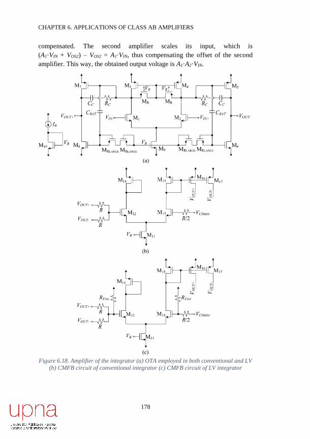
CHAPTER 6. APPLICATIONS OF CLASS AB AMPLIFIERS
178
compensated. The second amplifier scales its input, which is
(A1·VIN + VOS2) – VOS2 = A1·VIN, thus compensating the offset of the second
amplifier. This way, the obtained output voltage is A1·A2·VIN.
Figure 6.18. Amplifier of the integrator (a) OTA employed in both conventional and LV
(b) CMFB circuit of conventional integrator (c) CMFB circuit of LV integrator

CHAPTER 6. APPLICATIONS OF CLASS AB AMPLIFIERS
179
Figure 6.19. Preamplifier of the Delta-Sigma converter
Single-stage differential pairs with LCFMB active load have been
employed as amplifiers, which are shown in Figure 6.20. Since the amplitude of
input differential signal is small, there is no need to modify the topology to
achieve rail-to-rail operation, thus the same schematic works for both
conventional and low supply voltage versions.
Figure 6.20. Single stage amplifier used in pre-amplifier block
After the preamplifier, a track and latch stage is employed as
comparator. Its schematic is displayed in Figure 6.21. When VIN+ > VIN-,
transistors M24 and M26 are off, whereas M25 and M27 are on. In 1 switches SW8
are closed, the voltage at node B is VDD, and that of node A is VSS. However, in
2, the voltage at these nodes becomes VSS due to switches SW9. Thus, voltage
at node A is VSS but node B experiences swings between VDD (in 1) and VSS (in
2). Switches SW10 are closed a bit later than SW9, making voltage at node C to

CHAPTER 6. APPLICATIONS OF CLASS AB AMPLIFIERS
180
maintain a constant voltage VDD in both phases while node D toggles between
VSS (in 1) and VDD (in 2), just the opposite of node B. Finally, as SW11 close at
next 1 (a bit delayed), the inverted output is VSS for both phases, and VOUT is
VDD. When VIN+ < VIN-, nodes A and B exchange their behavior, as well as nodes
C and D. Note that when there is a transition at the output of the comparator, it
happens one cycle after input signals have changed. Delayed clocks have been
used to connect the inverters to ensure their proper operation. In addition, this
topology is also suitable for low supply voltages, as transistors are acting as
switches.
Figure 6.21. Track and Latch comparator
The last block to design is the 1-bit DAC. Although the output of the
Sigma Delta modulator is already a digital signal, its amplitude has to be
reconditioned in order to be comparable with that of the input signal.
Figure 6.22(a) indicates the conceptual scheme of the DAC. Its output must be
VREF+ or VREF-, depending on a control signal, which in this case is the output of
the Delta-Sigma modulator. The implementation of the DAC is shown in
Figure 6.22(b), employing transistors as switches.
Figure 6.22. 1-bit Digital-to-Analog converter
Two Delta-Sigma modulators are built with the previously presented
blocks: the first one will be supplied by two ±0.6 V complementary voltage

CHAPTER 6. APPLICATIONS OF CLASS AB AMPLIFIERS
181
sources, and the second one is the low-voltage version of the former, whose
supply voltages are half of the conventional, i.e. ±0.3 V. Bias current IB is
10 μA. Table 6.3 indicates the values of different devices employed. The
inverter block has been implemented in conventional configuration, whose
PMOS and NMOS transistors have aspect radios of 60 μm/210 nm and
30 μm/210 nm, respectively. Reference voltages VCMREF of Figure 6.18(b) and
Figure 6.18(c) are both connected to ground, as the modified LCFMB circuit
shifts the voltage at gates of differential pair thanks to RVDD. The reference
voltages VREF+ and VREF- of the conventional Sigma Delta modulator are
±0.45 V and that of the proposed one are ±225 mV, respectively.
Component Value Component Value
M1-M2 40 μm / 210nm MSW8 60 μm / 210 nm
M3-M4 75 μm / 210 nm MSW9 20 μm / 210 nm
M5, M7 150 μm / 210 nm MSW10-11 500nm / 130 nm
M6, M8 120 μm / 210 nm MSW12-15 1.5 μm / 160 nm
M9-M11 80 μm / 210 nm MRlarge 300 nm / 160 nm
M12-M13 40 μm / 210 nm MR 5 μm / 130 nm
M14-M17 75 μm / 210 nm R 50 k
M18-M19 40 μm / 210 nm RVDD 15 k
M20-M21 75 μm / 210 nm RC 5 k
M22-M23 80 μm / 210 nm RLCMFB 40 k
M24-M27 60 μm / 210 nm CC 4 pF
M28-M29 20 μm / 210 nm C1 1 pF
MSW1-4 500nm / 130 nm C2 3.5 pF
MSW5-7 1.5 μm / 160 nm C3 2 pF
Table 6.3. Parameter values of Sigma-Delta modulator
Figure 6.23 and Figure 6.24 show the response of both Delta-Sigma
modulators to a 50 kHz 450 mVpp and 225 mVpp sinusoidal signal, respectively.
These signals should be demodulated in order to obtain (𝑡). However, this
process requires a lot of samples (leading to a huge computational load).

CHAPTER 6. APPLICATIONS OF CLASS AB AMPLIFIERS
182
Thus, an improved Sigma Delta has been obtained by applying a low
voltage low power technique, which was explained in Section 2.2.1. Thanks to
this, the supply voltage was reduced to half of that of the conventional block.
Figure 6.23. Conventional Delta-Sigma response
Figure 6.24. Proposed Low-Voltage Delta-Sigma response

CHAPTER 6. APPLICATIONS OF CLASS AB AMPLIFIERS
183
6.4 Conclusions
In this Chapter, three low voltage subsystem blocks have been
introduced. First block is a low power buffer, which is based on switched
capacitors. The second and third blocks are related to A/D conversion: a Sample
and Hold and a Sigma Delta modulator. The three proposed circuits are capable
of operating in low voltage conditions, making them suitable for energy
harvesting supplied systems.

CHAPTER 6. APPLICATIONS OF CLASS AB AMPLIFIERS
184
Bibliography of the Chapter
[1] J. Crols and M. Steyaert, “Switched-opamp: an approach to realize full
CMOS switched-capacitor circuits at very low power supply voltages”,
IEEE Journal of Solid-State Circuits, vol. 29, no. 8, 1994.
[2] A. Baschirotto, R. Castello and G. P. Montagna, “Active series switch
for switched-opamp circuits”, Electronics Letters, vol. 34, no. 14,
1998.
[3] J. Ramirez-Angulo, R. G. Carvajal, J. Tombs and A. Torralba, “Simple
technique for opamp continuous-time 1 V supply operation”,
Electronics Letters, vol. 35, no. 4, 1999.
[4] K. R. Stafford, R. A. Blanchard and P. R. Gray, “A complete
monolithic sample/hold amplifier”, IEEE Journal of Solid-State
Circuits, vol. 9, no. 6,1974.
[5] J. Ramirez-Angulo, C. I. Lujan-Martinez, C. Rubia-Marcos,
R. G. Carvajal and A. Lopez-Martin, “Rail-to-rail fully differential
simple and hold based on differential difference amplifier”, Electronics
Letters, vol. 44, no. 11, 2008.

185
Chapter 7
CONCLUSIONS AND FUTURE
WORK
In this Chapter, the most significant results and conclusions reported
throughout this thesis are summarized. The objective of Section 7.1 is to provide
a compilation of the main contributions to verify the fulfillment of the objectives
proposed in Chapter 1. In addition, future research directions related to this work
are proposed and briefly analyzed in Section 7.2.
7.1 Conclusions
Almost all the work done in this Ph. D. thesis has been based on the
application of low voltage low power techniques to analog design, and more
specifically to amplifiers, in order to obtain different blocks suitable for systems
with strict energy constraints, such as those employing energy harvesting. The
motivation is the growing demand of portable devices supplied by batteries in
IoT scenarios, which require to extend the lifetime of the battery or even to get
rid of such battery in some cases. In the following paragraphs, general
conclusions are provided following the structure of this document, i.e. first the
proposed new cells are addressed to end with the design of complete subsystems.
Chapter 2 has presented the state of the art of low voltage low power
methodologies, in order to achieve class AB amplifiers with high current
efficiency and rail-to-rail operation. Note that these techniques can be applied

CHAPTER 7. CONCLUSIONS AND FUTURE WORK
186
at device level (in this case, at transistor level) or at circuit level. Special
attention has been paid to Quasi-Floating Gate (QFG) transistors, the adaptive
biasing of the input pair (especially that formed by two cross-coupled floating
batteries) and the Local Common Mode Feedback (LCMFB) configuration.
In Chapter 3, the conventional CMOS logic gate family has been
revisited and adapted to subthreshold operation by using QFGMOS transistors.
Besides, two applications of these logic gates have been presented: a ring
oscillator and a clock doubler. Thanks to QFGMOS transistors, the voltage
supply requirements have been relaxed, and faster subthreshold logic gates have
been obtained.
Several single-ended amplifiers have been proposed in Chapter 4,
which is formed by three subsections, depending on the topology these
amplifiers are based on: telescopic cascode amplifier, folded cascode amplifier
and recycling folded cascode. All the proposed amplifiers presented higher
transconductance (thus GBW), higher SR values, lower input referred noise
density (mainly caused by the higher Gm) and nearly ideal current efficiency
(CE). It is worth mentioning the particular case of a RFC combining an adaptive
bias scheme at the input stage and a Local Common-Mode Feedback topology
at the folding stage, which achieved an increase factor on the SR of 66 vs. the
conventional folded cascode amplifier. In Section 4.2, not only the proposed
OTAs have been compared, but also other opamps previously published by other
authors. In order to ease that comparison, two Figure of Merits have been
employed, evidencing the improvements of the proposed blocks.
Chapter 5 contains different blocks related to fully differential
amplifiers. First, an improved Common-Mode Feedback (CMFB) circuit has
been proposed, which has been used to control the output common-mode
voltage of a super class AB OTA. After that, several class AB fully differential
OTAs have been proposed, all of them with improved transconductance (thus
ADC and GBW) and SR. As happened in Chapter 4, a final Section has been
included, addressing a comparison of the proposed OTAs and other ones
previously published by other authors, in which the former ones presented
higher values of Figures of Merit.
Finally, subsystem level blocks have been presented in Chapter 6, two
of them related with Analog to Digital converters (ADCs): a Sample and Hold
and a Delta Sigma modulator. Apart from that, a low voltage buffer has been
proposed, which despite using switched capacitors, it is suitable for continuous

CHAPTER 7. CONCLUSIONS AND FUTURE WORK
187
time applications. In the three cases, although their supply voltages have been
decreased, they enhance their respective conventional versions.
7.2 Future Work
Although different proposals have been made throughout this thesis at
device, circuit and subsystem level, much work is still to be made. Some new
possible directions are specified below.
For some of the blocks, only simulation results have been provided, as
they have not been fabricated. Thus, these blocks can be fabricated in
order to validate their advantages by measurements.
Most of the prototype chips have been fabricated in a 0.5m CMOS
technology, which is very reliable but also old-fashioned and with large
threshold voltages. More modern technologies can be employed to
obtain faster designs able to operate at lower supply voltages.
The majority of the proposed amplifiers have been designed following
single-ended topologies. In Chapter 5, the advantages of fully
differential implementations have been enumerated, such as higher
input range and lower THD. Thus, the proposed amplifiers can be
redesigned with differential output in order to improve their features
even more.
Several amplifiers have been proposed at cell level, obtaining
improved performance when compared with conventional topologies.
These amplifiers can be employed at system level to take advantage of
its characteristics.
In Chapter 6, a low voltage Sigma Delta Modulator was presented.
However, only simulated time response graphs have been included.
Thus, a more in-depth analysis must be performed.

CHAPTER 7. CONCLUSIONS AND FUTURE WORK
188

189
Appendix A
SETUP DESCRIPTION
In this Appendix, the experimental setup employed for the different
measurements carried out is going to be explained. However, before addressing
the different setups, some extra circuitry will be described. When fully
differential OTAs are measured, two additional blocks may be needed
depending on the test equipment available: a voltage subtractor and a differential
signal generator.
Figure A.1. Subtractor circuit (a) Schematic (b) Implementation
A well-known structure of a subtractor is shown in Figure A.1(a). The
resulting output voltage is VOUT = VIN+-VIN-. Thanks to the use of an AMP03
Precision Unity-Gain Differential Amplifier from Analog Devices, an easy
implementation is obtained, as depicted in Figure A.1(b). Voltages V+ and V-

APPENDIX A: SETUP DESCRIPTION
190
represent the positive and negative supply voltages, respectively. These voltages
are defined in the datasheet of the AMP03, which are typically 15 V.
The second block is a differential signal generator. For AC
measurements, VIN+ = VCM + Vid/2 and VIN- = VCM – Vid/2 are required. However,
in practice, a vector signal analyzer is employed for AC input generation, which
provides a chirp signal in one of its ports. This signal must be converted from
single-ended to differential form. For that purpose, circuit in Figure A.2 is
used. The obtained output signals are
𝑉𝐼𝑁+ = 𝑉𝐶𝑀 +𝑅2
𝑅1𝑉𝑖𝑑 (A.1)
𝑉𝐼𝑁− = 𝑉𝐶𝑀 −𝑅2
𝑅1𝑉𝑖𝑑 (A.2)
As in the AMP03, R1 = R2 = 25 k, factor R2/R1 = 1. Thus, the
amplitude of the differential input voltage Vid should be half to compensate this
effect.
Figure A.2. Differential signal generator (a) Schematic (b) Implementation

APPENDIX A: SETUP DESCRIPTION
191
Figure A.3. Output current measurements setup (a) Single-ended (b) Fully-differential
The setup employed for output current measurements is depicted in
Figure A.3. The OTAs in open loop configuration are driven by the differential
output of an Agilent 33522A arbitrary waveform generator, and the output of
the device under test is connected to a transresistance amplifier for
voltage-to-current conversion. The resulting voltage is applied to a Textronix
TDS 5104 oscilloscope for capture and display. In the case of fully differential
topologies, a subtractor circuit is placed between the target OTA and the
transresistence amplifier, as shown in Figure A.3(b).
As shown in Figure A.4, for time-domain measurements the Agilent
33522A signal is applied to the OTAs in unity-gain closed-loop configuration
and the unbuffered output is directly connected to the TDS 5104 oscilloscope
using a conventional test probe. For distortion analysis the output signal is
applied to a Hewlett Packard 89410A Vector Signal Analyzer. Note that when
the topology of the amplifier is fully differential, the unity-gain close-loop
configuration requires four matched R resistors, which are always fabricated on-
chip.
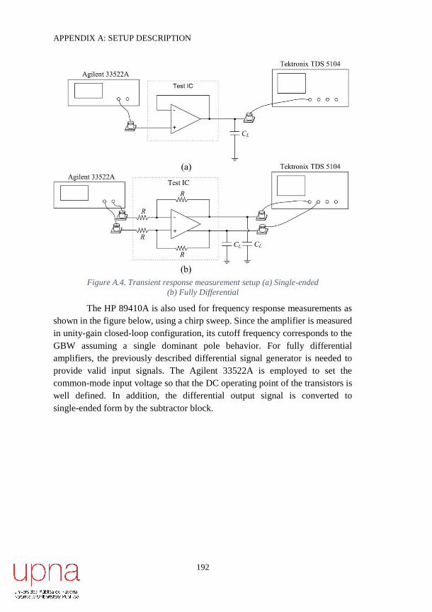
APPENDIX A: SETUP DESCRIPTION
192
Figure A.4. Transient response measurement setup (a) Single-ended
(b) Fully Differential
The HP 89410A is also used for frequency response measurements as
shown in the figure below, using a chirp sweep. Since the amplifier is measured
in unity-gain closed-loop configuration, its cutoff frequency corresponds to the
GBW assuming a single dominant pole behavior. For fully differential
amplifiers, the previously described differential signal generator is needed to
provide valid input signals. The Agilent 33522A is employed to set the
common-mode input voltage so that the DC operating point of the transistors is
well defined. In addition, the differential output signal is converted to
single-ended form by the subtractor block.
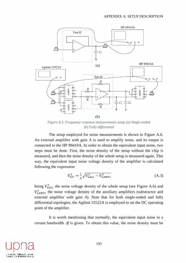
APPENDIX A: SETUP DESCRIPTION
193
Figure A.5. Frequency response measurements setup (a) Single-ended
(b) Fully differential
The setup employed for noise measurements is shown in Figure A.6.
An external amplifier with gain A is used to amplify noise, and its output is
connected to the HP 89410A. In order to obtain the equivalent input noise, two
steps must be done. First, the noise density of the setup without the chip is
measured, and then the noise density of the whole setup is measured again. This
way, the equivalent input noise voltage density of the amplifier is calculated
following the expression
𝑉𝑛𝐼𝐶2 =
1
𝐴√𝑉𝑛𝐴𝐿𝐿
2 − 𝑉𝑛𝐴𝑀𝑃𝑠2 (A.3)
being 𝑉𝑛𝐴𝐿𝐿2 the noise voltage density of the whole setup (see Figure A.6) and
𝑉𝑛𝐴𝑀𝑃𝑠2 the noise voltage density of the auxiliary amplifiers (substractor and
external amplifier with gain A). Note that for both single-ended and fully
differential topologies, the Agilent 33522A is employed to set the DC operating
point of the amplifier.
It is worth mentioning that normally, the equivalent input noise in a
certain bandwidth f is given. To obtain this value, the noise density must be

APPENDIX A: SETUP DESCRIPTION
194
integrated in f. Since the flicker noise is not considered (due to the relatively
high bandwidth of the tested devices) and the thermal noise is constant, the
input-referred noise is calculated as the product of the noise density and the
squared root of f.
Figure A.6. Noise measurements setup (a) Single-ended (b) Fully differential

195
Appendix B
NOISE ANALYSIS OF THE
IMPROVED RFC The most relevant noise sources in CMOS analog circuits are thermal
and flicker noise. Assuming operation in saturation, a simplified expression of
the mean square value of the noise current of a MOS transistor is [1]
𝐼𝑛2(𝑓) = 4𝛿𝑘𝐵𝑇𝑔𝑚 +
𝐾𝑓𝑔𝑚2
𝑊𝐿𝐶𝑜𝑥𝑓= 4𝛿𝑘𝐵𝑇𝑔𝑚 +
2𝜇𝐾𝑓𝐼𝐷
𝐿2𝑓 (B.1)
with kB the Boltzmann's constant, T the absolute temperature, μ the carrier
mobility and Kf a technology-dependent parameter which is also dependent on
device characteristics. Factor δ varies from 1/2 to 2/3 from weak to strong
inversion. The first and second terms in Equation B.1 correspond to the thermal
and flicker noise, respectively. The expression B.1 represents a good trade-off
between simplicity, accuracy and validity in all the inversion regions.
Assuming as usually that all noise sources are uncorrelated, and for
simplicity the same δ factor for all transistors, the input-referred thermal noise
of the FC OTA is
𝑣𝑛𝑡,𝑖𝑛𝐹𝐶2 =
2𝛿𝑘𝐵𝑇𝛥𝑓
𝑔𝑚1𝐴(2 +
𝑔𝑚3𝐴
𝑔𝑚1𝐴+
𝑔𝑚3𝐵
𝑔𝑚1𝐴+
𝑔𝑚9
𝑔𝑚1𝐴) (B.2)

APPENDIX B. NOISE ANALYSIS OF THE IMPROVED RFC
196
and that of the RFC OTA is
𝑣𝑛𝑡,𝑖𝑛𝑅𝐹𝐶2 =
8𝛿𝑘𝐵𝑇𝛥𝑓
𝑔𝑚1𝐴(1+𝐾)2 (1 + 𝐾2 + (1 + 𝐾)𝑔𝑚3𝐴
𝑔𝑚1𝐴+
𝑔𝑚9
𝑔𝑚1𝐴) (B.3)
which for the implemented value of K=3 becomes
𝑣𝑛𝑡,𝑖𝑛𝑅𝐹𝐶2 =
2𝛿𝑘𝐵𝑇𝛥𝑓
𝑔𝑚1𝐴(
5
2+
𝑔𝑚3𝐴
𝑔𝑚1𝐴+
1
4
𝑔𝑚9
𝑔𝑚1𝐴) (B.4)
The expression for the super class AB RFC OTA is
𝑣𝑛𝑡,𝑖𝑛𝐴𝐵2 =
2𝛿𝑘𝐵𝑇𝛥𝑓
𝑔𝑚1𝐴[
𝑔𝑚3𝐴+𝑔𝑚9
𝑔𝑚1𝐴(1+𝑔𝑚3𝐴𝑅)2 +1+2(𝑔𝑚3𝐴𝑅)2
(1+𝑔𝑚3𝐴𝑅)2
+1
𝑔𝑚1𝐴(
𝑔𝑚3𝐴𝑅
1+𝑔𝑚3𝐴𝑅)
2
(𝑔𝑚3𝐵 +1
𝛿𝑅)
] (B.5)
which for R>>1/gm3A becomes
𝑣𝑛𝑡,𝑖𝑛𝐴𝐵2 =
2𝛿𝑘𝐵𝑇𝛥𝑓
𝑔𝑚1𝐴[2 +
𝑔𝑚3𝐴
𝑔𝑚1𝐴+
1
𝛿𝑔𝑚1𝐴𝑅] (B.6)
Concerning flicker noise, assuming again uncorrelated noise sources
and the same Kf for all the transistors of the same type (NMOS or PMOS) the
resulting expression for the FC OTA is:
𝑉𝑛𝑓,𝑖𝑛𝐹𝐶2 (𝑓) =
2𝐾𝑓𝑝
𝐶𝑜𝑥𝑓𝑊1𝐿1[1 + (
𝐿1
𝐿9)
2
+ 2𝐾𝑓𝑛
𝐾𝑓𝑝
𝜇𝑛
𝜇𝑝(
𝐿1
𝐿3)
2
] (B.7)
and for the RFC OTA it is
𝑉𝑛𝑓,𝑖𝑛𝑅𝐹𝐶2 (𝑓) =
2𝐾𝑓𝑝
𝐶𝑜𝑥𝑓𝑊1𝐴𝐿1𝐴[
1+𝐾2
(1+𝐾)2 +2
(1+𝐾)2 (𝐿1𝐴
𝐿9)
2
+𝐾𝑓𝑛
𝐾𝑓𝑝
𝜇𝑛
𝜇𝑝
𝐾
1+𝐾(
𝐿1𝐴
𝐿3𝐵)
2 ] (B.8)
The input-referred flicker noise of the super class AB RFC OTA is
𝑉𝑛𝑓,𝑖𝑛𝐴𝐵2 (𝑓) =
𝐾𝑓𝑝
2𝐶𝑜𝑥𝑓𝑊1𝐴𝐿1𝐴(1+𝑔𝑚3𝐴𝑅)2
1 + 2 (𝐿1𝐴
𝐿9)
2
+ 3𝐾𝑓𝑛
𝐾𝑓𝑝
𝜇𝑛
𝜇𝑝(
𝐿1𝐴
𝐿3𝐵)
2
+
+(𝑔𝑚3𝐴𝑅)2 [2 +𝐾𝑓𝑛
𝐾𝑓𝑝
𝜇𝑛
𝜇𝑝(
𝐿1𝐴
𝐿3𝐵)
2
]
(B.9)
In this design, all the transistors were implemented with the same L (the
minimum one available in the technology), so that expressions for the flicker
noise of the FC OTA, RFC OTA with K=3 and super class AB RFC OTA with
R>>1/gm3A are

APPENDIX B. NOISE ANALYSIS OF THE IMPROVED RFC
197
𝑉𝑛𝑓,𝑖𝑛𝐹𝐶2 (𝑓) =
4𝐾𝑓𝑝
𝐶𝑜𝑥𝑓𝑊1𝐿1(1 +
𝐾𝑓𝑛
𝐾𝑓𝑝
𝜇𝑛
𝜇𝑝) (B.10)
𝑉𝑛𝑓,𝑖𝑛𝑅𝐹𝐶2 (𝑓) =
4𝐾𝑓𝑝
𝐶𝑜𝑥𝑓𝑊1𝐴𝐿1𝐴
3
8(1 +
𝐾𝑓𝑛
𝐾𝑓𝑝
𝜇𝑛
𝜇𝑝) (B.11)
𝑉𝑛𝑓,𝑖𝑛𝐴𝐵2 (𝑓) =
4𝐾𝑓𝑝
𝐶𝑜𝑥𝑓𝑊1𝐴𝐿1𝐴
3
8(
2
3+
1
3
𝐾𝑓𝑛
𝐾𝑓𝑝
𝜇𝑛
𝜇𝑝) (B.12)

APPENDIX B. NOISE ANALYSIS OF THE IMPROVED RFC
198
Bibliography
[1] D. A. Johns and K. Martin, “Analog integrated circuit design”, John
Wiley & Sons, 1997.
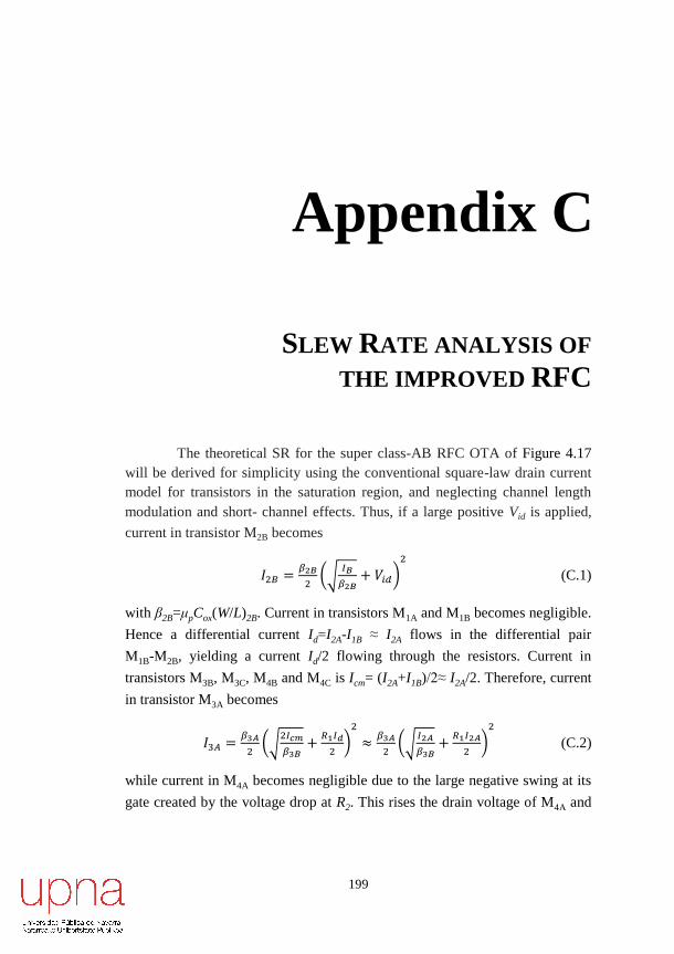
199
Appendix C
SLEW RATE ANALYSIS OF
THE IMPROVED RFC
The theoretical SR for the super class-AB RFC OTA of Figure 4.17
will be derived for simplicity using the conventional square-law drain current
model for transistors in the saturation region, and neglecting channel length
modulation and short- channel effects. Thus, if a large positive Vid is applied,
current in transistor M2B becomes
𝐼2𝐵 =𝛽2𝐵
2(√
𝐼𝐵
𝛽2𝐵+ 𝑉𝑖𝑑)
2
(C.1)
with β2B=μpCox(W/L)2B. Current in transistors M1A and M1B becomes negligible.
Hence a differential current Id=I2A-I1B ≈ I2A flows in the differential pair
M1B-M2B, yielding a current Id/2 flowing through the resistors. Current in
transistors M3B, M3C, M4B and M4C is Icm= (I2A+I1B)/2≈ I2A/2. Therefore, current
in transistor M3A becomes
𝐼3𝐴 =𝛽3𝐴
2(√
2𝐼𝑐𝑚
𝛽3𝐵+
𝑅1𝐼𝑑
2)
2
≈𝛽3𝐴
2(√
𝐼2𝐴
𝛽3𝐵+
𝑅1𝐼2𝐴
2)
2
(C.2)
while current in M4A becomes negligible due to the large negative swing at its
gate created by the voltage drop at R2. This rises the drain voltage of M4A and
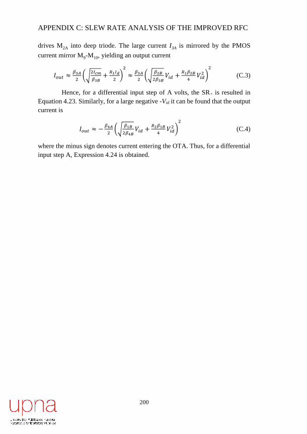
APPENDIX C: SLEW RATE ANALYSIS OF THE IMPROVED RFC
200
drives M2A into deep triode. The large current I3A is mirrored by the PMOS
current mirror M9-M10, yielding an output current
𝐼𝑜𝑢𝑡 ≈𝛽3𝐴
2(√
2𝐼𝑐𝑚
𝛽3𝐵+
𝑅1𝐼𝑑
2)
2
≈𝛽3𝐴
2(√
𝛽2𝐵
2𝛽3𝐵𝑉𝑖𝑑 +
𝑅1𝛽2𝐵
4𝑉𝑖𝑑
2 )2
(C.3)
Hence, for a differential input step of A volts, the SR+ is resulted in
Equation 4.23. Similarly, for a large negative -Vid it can be found that the output
current is
𝐼𝑜𝑢𝑡 ≈ −𝛽4𝐴
2(√
𝛽1𝐵
2𝛽4𝐵𝑉𝑖𝑑 +
𝑅2𝛽1𝐵
4𝑉𝑖𝑑
2 )2
(C.4)
where the minus sign denotes current entering the OTA. Thus, for a differential
input step A, Expression 4.24 is obtained.

201
Appendix D
INTRODUCTION TO A/D
CONVERSION
Nowadays, analog and digital signals have to coexist, as both are used
to transmit information by transforming it into electric signals. The difference
between analog and digital technologies is that in analog technology,
information is translated into electric signals of varying amplitude, whereas in
digital domain, translation of information is into binary format, represented by
two different amplitude levels.
Conversion between the analog and digital domain is a common
process in communication systems, either from digital to analog domain, such
as the reproduction of an mp3 audio file though a speaker, or from analog to
digital, e.g. a sound picked up by a microphone or light entering a digital camera.
As its name indicates, Analog-to-Digital converters (ADC) convert
analog information into a digital signal, making these discrete data suitable for
digital systems [1]. As Figure D.1 displays [1], the conversion implies three
steps: sampling, quantization and coding.

APPENDIX D: INTRODUCTION TO A/D CONVERSION
202
Figure D.1. Analog to Digital Conversion Process
Analog signals are characterized by being continuous in amplitude (and
usually also in time) and it is necessary to convert them to a sequence of numbers
that are only defined at determined (or discrete) instants of time, which are
proportional to the sampling period TS [1]. A discrete-time signal x*(t) can be
represented by a sampled continuous-time signal x(t) as:
𝑥∗(𝑡) = ∑ 𝑥(𝑡)𝛿(𝑡 − 𝑛𝑇)∞𝑛=−∞ (D.1)
where (t) is known as Dirac’s delta, and is defined as (t) = 1 only for t = 0,
and 0 in any other case.
Most ADCs can be divided into two groups: Nyquist rate converters
and oversampling converters. In the former ones, the maximum frequency of the
analog signal is slightly less than the Nyquist frequency, fN = fS/2, where fS is the
sampling frequency, whereas the latter ones perform the sampling process at a
much higher rate, fN << fS.
Figure D.2. Conventional Analog to Digital Conversion Process
A very common practice, as shown in Figure D.2, is to use an anti-
aliasing filter before sampling the signal. The anti-aliasing filter consists on a
low-pass filter whose response is flat over the frequency band of interest and
attenuates the frequencies above the Nyquist frequency. This way, signal
distortion due to aliasing is avoided. Figure D.3(a) and Figure D.3(b) show
aliasing distortion and the effects of the anti-aliasing filter, respectively [1].
After an anti-aliasing filter, a Sample and Hold circuit is employed
(Figure D.2). The purpose of this block is to maintain its output constant

APPENDIX D: INTRODUCTION TO A/D CONVERSION
203
between samples so that the signal can be quantized properly. If the output of
the sample and hold varies during TS, it can limit the performance of the ADC
converter subsystem.
(a)
(b)
Figure D.3. Aliasing distortion and result of using an anti-aliasing filter
The final block of a conventional ADC is the quantizer. It compares the
sampled analog signal to a set of reference levels, which are assigned to a digital
code. Depending on the result of the comparison, a digital encoder generates the
code corresponding to the level the input signal is closest to. The number of
quantization levels is dependent on the number of bits of resolution, N = 2B,
being N the number of voltage intervals and B the number of bits used by the
encoder. One of the most relevant parameters of an ADC is the resolution, which
is the minimum change in voltage required to guarantee a change in the output
code level. The voltage resolution is the overall voltage measurement range
divided by the number of intervals: Q = EFSR/N, with EFSR the full scale voltage
range or span, given by the difference between the upper and lower voltages that

APPENDIX D: INTRODUCTION TO A/D CONVERSION
204
can be coded: EFSR = VRefHi – VRefLow. This Q value is also known as Less
Significant Bit, or LSB. The greater the number of bits N, the smaller the error
of quantization, improving the accuracy [3].
Hence, the relationship between the sampled discrete signal x(n), the
sampled continuous signal x*(t) and the quantization noise or quantization error
is:
𝑥(𝑛) = 𝑥∗(𝑡) + 𝑒(𝑛) (D.2)
When the input signal is low (comparable to LSB), the quantization
error is dependent on the input signal, resulting in distortion, known as dither.
This distortion is created after the anti-aliasing filter, and if they are above half
the sample rate, they will alias back into the band of interest. In order to make
quantization error independent of the input signal, noise with an amplitude of
2·Q is often added to the signal, reducing signal to noise ratio (SNR), but ideally,
completely eliminating the distortion.
However, in the typical case where the original signal is much larger
than one LSB, the quantization error is not significantly correlated with the
signal, and has an approximately uniform distribution. Its value depends on the
quantization method: in the rounding case, the quantization error has a mean of
zero and the RMS value is the standard deviation of this distribution, given by
𝜎𝑒 = (1 √12⁄ ) · 𝑄 ≈ 0.289 · 𝑄, whereas in the truncation case, the mean is
𝜇𝑒 = (1 2⁄ ) · 𝑄 and the RMS value is 𝜎𝑒 = (1 √3⁄ ) · 𝑄. From the standard
deviation, quantization noise power, or variance is directly obtained as 𝜎𝑒2.
Since the noise power 𝜎𝑒2 is spread over the entire frequency range
equally, noise power spectral density can be expressed as 𝑁(𝑓) = 𝜎𝑒2/𝑓𝑠. If the
input signal is larger than the LSB step, the noise power spectral density is
defined in Equation D.3. In addition, Figure D.4 shows the noise spectrum of
Nyquist samplers.
𝑁(𝑓) = 𝑄2
12𝑓𝑠 (D.3)

APPENDIX D: INTRODUCTION TO A/D CONVERSION
205
Figure D.4. Noise PDF of Nyquist samplers
On the other hand, oversampling converters present some benefits
versus Nyquist samplers. One of them concerns the anti-aliasing filter. Nyquist-
rate converters require a low pass filter with stringent requirements, as its pass-
band response must be flat with not phase distortion (linear phase), and for
frequencies above its cutoff frequency, the frequency response must decay
abruptly, which in practice is difficult to achieve. Nevertheless, if the sampling
rate is N·fS, the requirements of the anti-aliasing filter are relaxed, as the
transition band of the filter can be much wider.
Besides, oversampling has beneficial effects on noise power, because
the total noise power for both samplers is the same (defined in Equation D.3),
but the percentage of this noise that is in the bandwidth of interest in
oversampling converters is smaller, which is defined by Equation D.4. The
bigger FS compared to fB, the smaller the noise. This concept is depicted in
Figure D.5.
𝑁𝐵 = ∫ 𝑁(𝑓)𝑑𝑓𝑓𝐵
−𝑓𝐵=
𝑄2
12
2𝑓𝐵
𝐹𝑠 (D.4)
Figure D.5. Noise Spectrum of Oversampling A/D Converters
Delta-Sigma modulation is one of the most effective forms of
conversion in the data converter world. Its applications include communication
systems, professional audio and precision measurements. But for a better
understanding, here is a brief explanation about how delta modulation works.
Figure D.6 includes delta modulation and demodulation schemes and their
corresponding signals. A higher transmission efficiency is achieved by

APPENDIX D: INTRODUCTION TO A/D CONVERSION
206
quantifying only the changes (delta) in value between consecutive samples,
rather than the actual samples themselves, assuming that contiguous samples are
highly correlated.
Figure D.6. Delta modulation (a) Modulator (b) Demodulator
The integrator of the feedback loop works as a predictor, as the output
of the integrator tries to predict input. The difference between the input x(t) and
the predicted signals (t) (also known as prediction error) is quantized and used
to make the next prediction. In order to recover the analog input signal, the
receiver must accumulate the bits and low pass filter that signal.

APPENDIX D: INTRODUCTION TO A/D CONVERSION
207
Figure D.7. Delta-Sigma Modulation (a) Two-integrators (b) Only one integrator
However, delta modulation requires two integrators for modulation and
demodulation. Since integration is a linear operation, the second integrator can
be moved before the modulator without altering the overall characteristics. In
addition, the two integrators can be combined into a single integrator by the
linear operation property. Figure D.7 shows this transformation. Scheme in
Figure D.7(b) is known as Delta-Sigma modulator, or -.
Sigma-Delta converters present a very advantageous feature. They
perform a quantization noise-shaping, resulting in an improved output signal.
This property is very useful in signal processing applications. When the -
modulator is analyzed in s-domain (see Figure D.8), the integrator becomes 1/s.
Figure D.8. S-Domain analysis of Sigma-Delta Modulator
If signal transfer function is calculated, a low-pass filter response is
observed, while as for the noise transfer function, a high-pass filter is obtained.
Equations D.5 and D.6 express signal and noise transfer functions respectively.

APPENDIX D: INTRODUCTION TO A/D CONVERSION
208
Hence, the input signal does not change as long as its frequency is not higher
than the low-pass filter cutoff frequency and the noise is pushed to higher
frequencies, so most of it is rejected by the low-pas filter.
𝑌(𝑠) = [𝑋(𝑠) − 𝑌(𝑠)]1
𝑠→
𝑌(𝑠)
𝑋(𝑠)=
1
𝑠
1+1
𝑠
=1
𝑠+1 (D.5)
𝑌(𝑠) = −𝑌(𝑠)1
𝑠+ 𝑁(𝑠) →
𝑌(𝑠)
𝑁(𝑠)=
1
1+1
𝑠
=𝑠
𝑠+1 (D.6)

APPENDIX D: INTRODUCTION TO A/D CONVERSION
209
Bibliography
[1] B. Razavi, “Design of analog CMOS integrated circuits”,
McGraw-Hill, 2001.
[2] S. Park, “Principles of Sigma-Delta Modulation for Analog-to-Digital
Converters”, Motorola.
[3] S. Haykin and M. Moher, “Introduction to Analog and Digital
Communications”, John Wiley & Sons, 2nd Edition, 2007.
[4] R. Lyons, “Understanding Digital Signal Processing”, Prentice Hall,
2001.

APPENDIX D: INTRODUCTION TO A/D CONVERSION
210

211
LIST OF PUBLICATIONS
International Journals
1. J. M. Algueta-Miguel, A. Lopez-Martin, M. P. Garde, C. A. De la Cruz
and J. Ramirez-Angulo, “±0.5 V 15 μW recycling folded cascode
amplifier with 34767 MHz·pF/mA FOM”, IEEE Solid-State Circuits
Letters, Jan. 2019.
2. M. P. Garde. A. Lopez-Martin, R. G. Carvajal, J. A. Galan and
J. Ramirez-Angulo, “Super class AB RFC OTA using nonlinear current
mirrors”, Electronics Letters, vol. 54, no. 23, pp. 1317-1318,
Nov. 2018.
3. M. P. Garde. A. J. Lopez-Martin, R. G. Carvajal and
J. Ramirez-Angulo, “Super class AB RFC OTA with adaptive local
common-mode feedback”, Electronics Letters, vol. 54, no. 22,
pp. 1272-1274, Nov. 2018.
4. M. P. Garde. A. Lopez-Martin, R. G. Carvajal and J. Ramirez-Angulo,
“Super class AB recycling folded cascode OTA”, IEEE Journal of
Solid-State Circuits, vol. 53, no. 9, pp. 2614-2623, Jun. 2018.
5. A. Lopez-Martin, M. P. Garde, J. M. Algueta, C. A. De la Cruz-Blas,
R. G. Carvajal and J. Ramirez-Angulo, “Enhanced single-stage folded
cascode OTA suitable for large capacitive loads”, IEEE Transactions
on Circuits and Systems II: Express Briefs, vol. 65, no. 4, pp. 441-445,
Apr. 2018.

LIST OF PUBLICATIONS
212
6. M. P. Garde, A. Lopez-Martin and J. Ramirez-Angulo,
“Power-efficient class AB telescopic cascode opamp”, Electronics
Letters, vol. 51, no. 10, pp- 620-622, May 2018.
7. J. M. Saso, A. Lopez-Martin, M. P. Garde and J. Ramirez-Angulo,
“Power-efficient single-stage class AB fully differential amplifier”,
Electronics Letters, vol. 53, no. 19, pp. 1298-1300, Sep. 2017.
8. A. Lopez-Martin, M. P. Garde and J. Ramirez-Angulo, “Class AB
differential difference amplifier for enhanced common-mode
feedback”, Electronics Letters, vol. 53, no. 7, pp. 454-456, Mar. 2017.
International Conferences
1. M. P. Garde, A. Lopez-Martin, R. G. Carvajal and J. Ramirez-Angulo,
“Micropower single-stage amplifier based on adaptive biasing and
class AB current follower”, XXXIII Conference on Design of Circuits
and Integrated Systems (DCIS 2018), Lyon, France, 2018.
2. M. Pilar Garde, A. López-Martín, D. Orradre and J. Ramirez-Angulo,
“Ultra-low power subthreshold quasi floating gate CMOS logic family
for energy harvesting”, 28th International Symposium on Power and
Timing Modeling, Optimization and Simulation (PATMOS), Platja
d’Aro, Spain, 2018.
3. M. P. Garde, A. Lopez-Martin, R. G. Carvajal and J. Ramirez-Angulo,
“Folded cascode OTA with 5540 MHz·pF/mA FoM”, IEEE
International Symposium on Circuits and Systems (ISCAS), Florence,
Italy, 2018.

LIST OF PUBLICATIONS
213
4. A. Lopez-Martin, M. P. Garde, R. G. Carvajal and J. Ramirez-Angulo,
“On the optimal current followers for wide-swing current-efficient
amplifiers”, IEEE International Symposium on Circuits and Systems
(ISCAS), Florence, Italy, 2018.
5. J. M. Algueta, A. Lopez-Martin, C. A. De la Cruz Blas, M. P. Garde,
J. R. Garcia-Oya, J. Garcia-Doblado, F. Muñoz-Chavero, V. Baena-
Lecuyer and E. Hidalgo-Fort, “Ultrasonic communication through
metallic walls for monitoring applications”, 32nd Conference on Design
of Circuits and Integrated Systems (DCIS), Barcelona, Spain, 2017.
6. A. Lopez-Martin, M. P. Garde and Jaime Ramirez-Angulo,
“Micropower class AB folded cascode OTA”, 32nd Conference on
Design of Circuits and Integrated Systems (DCIS), Barcelona, Spain,
2017.
7. C. A. De La Cruz-Blas, M. P. Garde and A. Lopez-Martin, “Super class
AB transconductor with slew-rate enhancement using QFG”, 2017
European Conference on Circuit Theory and Design (ECCTD),
Catania, Italy, 2017.
8. M. P. Garde, A. Lopez-Martin and J. Ramirez-Angulo, “Enhanced
differential super class AB OTA”, 13th Conference on PhD Research
in Microelectronics and Electronics (PRIME), Taormina, Italy, 2017.
9. M. P. Garde, A. Lopez-Martin and J. Ramirez-Angulo, “Improved
common-mode feedback based on LCMFB techniques”,
13th Conference on PhD Research in Microelectronics and Electronics
(PRIME), Taormina, Italy, 2017.

LIST OF PUBLICATIONS
214
10. M. P. Garde, A. Lopez-Martin and J. Ramirez-Angulo, “A power
efficient fully differential super class AB OTA”, 31st Conference on
Design of Circuits and Integrated Systems (DCIS), Granada, Spain,
2016.
11. J. M. Saso, A. Lopez-Martin and M. P. Garde, “Single-stage class AB
fully-differential amplifier with high current efficiency”,
31st Conference on Design of Circuits and Integrated Systems (DCIS),
Granada, Spain, 2016.
12. A. Lopez-Martin, D. Orradre, M. P. Garde, P. Sanchis, E. Gubia, G.
Perez, D. Astrain and J. Ramirez-Angulo, “Energy-harvesting
microsystems based on the QFG MOS transistors”, 15th International
Conference on Environment and Electrical Engineering (EEEIC),
Rome, Italy, 2015.
13. D. Orradre, A. Lopez-Martin, M. P. Garde, J. Ramirez-Angulo and R.
G. Carvajal, “High-performance digital subthreshold logic”,
29th Conference on Design and Integrated Systems (DCIS), Madrid,
Spain, 2014.