Design of an Optimized Low Power Vedic Multiplier Unit for ...Vedic Mathematics is a set of...
75
Design of an Optimized Low Power Vedic Multiplier Unit for Digital Signal Processing Applications A Project Report submitted by Nandita Bhaskhar Roll no - EDM10B009 in partial fulfillment for the award of the degree of Bachelor of Technology in Electronics Engineering (Design & Manufacturing) Indian Institute of Information Technology Design & Manufacturing, Kancheepuram Chennai May, 2014
-
Upload
truongthuan -
Category
Documents
-
view
219 -
download
2
Transcript of Design of an Optimized Low Power Vedic Multiplier Unit for ...Vedic Mathematics is a set of...

Design of an Optimized Low PowerVedic Multiplier Unit
for Digital Signal ProcessingApplications
A Project Report
submitted by
Nandita BhaskharRoll no - EDM10B009
in partial fulfillment for the award of the degreeof
Bachelor of Technology
in
Electronics Engineering(Design & Manufacturing)
Indian Institute of Information TechnologyDesign & Manufacturing, Kancheepuram
Chennai
May, 2014

BONAFIDE CERTIFICATE
Certified that this project report titled Design of an Optimized Low Power Vedic
Multiplier Unit for Digital Signal Processing Applications is the bonafide work
of Ms. Nandita Bhaskhar who carried out the research under my guidance. Certified
further, that to the best of my knowledge the work reported herein does not form part
of any other project report or dissertation on the basis of which a degree or award was
conferred on an earlier occasion on this or any other candidate.
(Dr. Binsu J Kailath)
Project GUIDE
Assistant Professor
IIITD&M, Kancheepuram
Chennai 600-127
Place: Chennai
Date: 26th May, 2014

ACKNOWLEDGEMENTS
I am deeply grateful to my guide and mentor, Prof. Dr. Binsu J Kailath, for her
invaluable guidance, support and encouragement, without which this project could not have
been completed successfully. Her incredible patience and helpful advice, combined with her
care and friendship made my project work truly satisfying and pleasurable. I am indeed
very privileged to have got this opportunity to work with her.
I would also like to thank all the faculty members in the Electronics Department for their
timely suggestions, positive criticism and insightful remarks which encouraged me to give
more depth to my project. I am very grateful to my lab technicians and other staff members
for obligingly acquiescing to all my requests. Their assistance and support truly made my
work easier. I’d like to extend my gratitude to the Computer Science Department for let-
ting me use the labs full time. And I thank the Director for giving me this great opportunity.
The acknowledgements wouldn’t be complete without mentioning my family and friends.
I’d like to thank my parents and sister for giving me their love & support despite all my
grouchiness and I’d like to extend it to my close friends who put up with my peeves very
cheerfully. And I am forever indebted to a very special friend of mine for encouraging me
throughout & for coming to my rescue especially when I needed it. I couldn’t have done my
report without you.
Nandita Bhaskhar
i

ABSTRACT
Digital multipliers play a crucial role in various Digital Signal Processing units. They
carry the major responsibility of power expenditure in the system and ultimately determine
its speed. As a result, it is always beneficial to develop high performance, low power
multipliers.
Vedic Mathematics is a set of mathematical rules, derived from ancient Indian scripts
that makes arithmetic calculations extremely fast and simple. There are 16 rules or Sutras
expounded in Vedic Mathematics. This report presents novel designs of a multiplier based
on the Vedic Sutras on multiplication - Urdhva Tiryakbhyam and Nikhilam.
The objective of this report is to develop an optimum Vedic multiplier for 128−bit inputs.
Various fresh algorithms and strategies based on both the sutras as well as a combination
of them are propounded and implemented to develop the most optimum multiplier in terms
of power consumption, delay and area occupied. The proposed multipliers are designed for
synthesis using Carry Look Ahead Adders and compared with other existing multipliers
like Array, Booth and Modified Booth multipliers and the performances are evaluated. The
design of a novel integrated 128− bit multiplier is presented along with its mathematical
analysis of power and is validated by its optimum time delay, area occupancy and minimum
power consumption of 4.971 ns, 75013 nm2 and 28.73 mW respectively.
KEYWORDS: Integrated digital multiplier, Vedic Mathematics, Vedic Sutras, Urdhva
Tiryakbyam, Nikhilam, low power, optimum area, reduced time delay, 128 − bit, Array,
Booth, Modified Booth
ii

Contents
Acknowledgements i
Abstract ii
List of Tables vi
List of Figures viii
List of Abbreviations ix
List of Notations x
1 Introduction 11.1 Vedic Mathematics - An Overview . . . . . . . . . . . . . . . . . . . . . . . 31.2 Motivation . . . . . . . . . . . . . . . . . . . . . . . . . . . . . . . . . . . . 31.3 Objective . . . . . . . . . . . . . . . . . . . . . . . . . . . . . . . . . . . . 51.4 Organization of the Report . . . . . . . . . . . . . . . . . . . . . . . . . . . 6
2 Literature Review 7
3 Theoretical Background – Algorithms 103.1 Urdhva Tiryakbhyam . . . . . . . . . . . . . . . . . . . . . . . . . . . . . . 103.2 Nikhilam . . . . . . . . . . . . . . . . . . . . . . . . . . . . . . . . . . . . . 123.3 Karatsuba-Ofman Algorithm . . . . . . . . . . . . . . . . . . . . . . . . . . 133.4 Carry Look Ahead Adder . . . . . . . . . . . . . . . . . . . . . . . . . . . 15
4 Design & Implementation 194.1 Synthesizable Code for Hardware Efficiency . . . . . . . . . . . . . . . . . 194.2 Vedic UT . . . . . . . . . . . . . . . . . . . . . . . . . . . . . . . . . . . . 204.3 Scaling – The overall plan . . . . . . . . . . . . . . . . . . . . . . . . . . . 20
4.3.1 Where have the optimizations taken place? . . . . . . . . . . . . . . 224.4 UT Squaring . . . . . . . . . . . . . . . . . . . . . . . . . . . . . . . . . . 22
4.4.1 Scaling – Adapted for Squares . . . . . . . . . . . . . . . . . . . . . 224.5 Proposed Design D . . . . . . . . . . . . . . . . . . . . . . . . . . . . . . . 234.6 Thresholding Nikhilam . . . . . . . . . . . . . . . . . . . . . . . . . . . . . 244.7 Successive Nikhilam . . . . . . . . . . . . . . . . . . . . . . . . . . . . . . . 25
iii

5 Sampoornam – the Proposed Integrated Multiplier 285.1 Sampoornam: Specifications . . . . . . . . . . . . . . . . . . . . . . . . . . 285.2 Sampoornam: Logic . . . . . . . . . . . . . . . . . . . . . . . . . . . . . . 295.3 Sampoornam: Implementation . . . . . . . . . . . . . . . . . . . . . . . . . 305.4 Sampoornam: Advantages . . . . . . . . . . . . . . . . . . . . . . . . . . . . 31
6 Simulations and Results 326.1 Vedic UT . . . . . . . . . . . . . . . . . . . . . . . . . . . . . . . . . . . . 32
6.1.1 RTL Schematics . . . . . . . . . . . . . . . . . . . . . . . . . . . . . 326.1.2 RTL Results . . . . . . . . . . . . . . . . . . . . . . . . . . . . . . . 36
6.2 Vedic Square . . . . . . . . . . . . . . . . . . . . . . . . . . . . . . . . . . 366.2.1 RTL Schematics . . . . . . . . . . . . . . . . . . . . . . . . . . . . . 366.2.2 RTL Results . . . . . . . . . . . . . . . . . . . . . . . . . . . . . . . 38
6.3 Design D . . . . . . . . . . . . . . . . . . . . . . . . . . . . . . . . . . . . . 386.3.1 RTL Results . . . . . . . . . . . . . . . . . . . . . . . . . . . . . . . 38
6.4 Nikhilam GG . . . . . . . . . . . . . . . . . . . . . . . . . . . . . . . . . . 386.4.1 RTL Schematics . . . . . . . . . . . . . . . . . . . . . . . . . . . . . 386.4.2 RTL Results . . . . . . . . . . . . . . . . . . . . . . . . . . . . . . . 40
6.5 Nikhilam - SG . . . . . . . . . . . . . . . . . . . . . . . . . . . . . . . . . . 406.5.1 RTL Schematics . . . . . . . . . . . . . . . . . . . . . . . . . . . . . 406.5.2 RTL Results . . . . . . . . . . . . . . . . . . . . . . . . . . . . . . . 42
6.6 Nikhilam SS . . . . . . . . . . . . . . . . . . . . . . . . . . . . . . . . . . . 426.6.1 RTL Schematics . . . . . . . . . . . . . . . . . . . . . . . . . . . . . 426.6.2 RTL Results . . . . . . . . . . . . . . . . . . . . . . . . . . . . . . . 43
6.7 Logic Block . . . . . . . . . . . . . . . . . . . . . . . . . . . . . . . . . . . 446.7.1 RTL Schematics . . . . . . . . . . . . . . . . . . . . . . . . . . . . . 446.7.2 RTL Results . . . . . . . . . . . . . . . . . . . . . . . . . . . . . . . 44
6.8 CLA Blocks . . . . . . . . . . . . . . . . . . . . . . . . . . . . . . . . . . . 456.8.1 RTL Analysis . . . . . . . . . . . . . . . . . . . . . . . . . . . . . . 45
6.9 Test Bench Output . . . . . . . . . . . . . . . . . . . . . . . . . . . . . . . 45
7 Inferences 477.1 Comparison –
Vedic UT, Vedic Square & Design D . . . . . . . . . . . . . . . . . . . . . 477.2 A look at the 3 cases of Nikhilam . . . . . . . . . . . . . . . . . . . . . . . 497.3 Analytical Comparisons with the Vedic UT . . . . . . . . . . . . . . . . . . 507.4 Analysis of the Logic Block and CLA Adder . . . . . . . . . . . . . . . . . . 51
7.4.1 Logic Block . . . . . . . . . . . . . . . . . . . . . . . . . . . . . . . . 517.4.2 CLA Adder . . . . . . . . . . . . . . . . . . . . . . . . . . . . . . . . 51
8 Comparison with Existing Work 53
9 Power Analysis 559.1 Power analysis – Sampoornam . . . . . . . . . . . . . . . . . . . . . . . . . 56
iv

10 Conclusion 5810.1 Future Scope . . . . . . . . . . . . . . . . . . . . . . . . . . . . . . . . . . 59
Bibliography 60
Appendix A - Vedic Sutras 62
Appendix B - Cadence Encounter 63
v

List of Tables
3.1 Adder Comparison – N : input size, k: group size . . . . . . . . . . . . . . 18
4.1 Thresholds for various multipliers . . . . . . . . . . . . . . . . . . . . . . . 244.2 Multiplication of m× n, base r . . . . . . . . . . . . . . . . . . . . . . . . 244.3 Multiplication of m× n, base r . . . . . . . . . . . . . . . . . . . . . . . . 254.4 Multiplication of m× n, base r . . . . . . . . . . . . . . . . . . . . . . . . 254.5 Nikhilam – 1111× 1111, base = 1000 . . . . . . . . . . . . . . . . . . . . . 264.6 Total No. of Adders Required – Successive Nikhilam . . . . . . . . . . . . 27
5.1 Designs and their input constraints . . . . . . . . . . . . . . . . . . . . . . 295.2 Priority Encoder – Output . . . . . . . . . . . . . . . . . . . . . . . . . . . 30
6.1 Vedic UT . . . . . . . . . . . . . . . . . . . . . . . . . . . . . . . . . . . . 366.2 Vedic Square . . . . . . . . . . . . . . . . . . . . . . . . . . . . . . . . . . 386.3 Design D . . . . . . . . . . . . . . . . . . . . . . . . . . . . . . . . . . . . . 386.4 Nikh GG . . . . . . . . . . . . . . . . . . . . . . . . . . . . . . . . . . . . . 406.5 Nikh SG . . . . . . . . . . . . . . . . . . . . . . . . . . . . . . . . . . . . . 426.6 Nikh SS . . . . . . . . . . . . . . . . . . . . . . . . . . . . . . . . . . . . . 436.7 Logic . . . . . . . . . . . . . . . . . . . . . . . . . . . . . . . . . . . . . . . 446.8 CLA Analysis . . . . . . . . . . . . . . . . . . . . . . . . . . . . . . . . . . 45
7.1 Vedic UT to Vedic Square: % reduction . . . . . . . . . . . . . . . . . . . . 507.2 Vedic UT to Design D: % reduction . . . . . . . . . . . . . . . . . . . . . . 507.3 Vedic UT to Nikhilam (maximum): % reduction . . . . . . . . . . . . . . . 50
8.1 As reported in Literature . . . . . . . . . . . . . . . . . . . . . . . . . . . . 538.2 Vedic UT . . . . . . . . . . . . . . . . . . . . . . . . . . . . . . . . . . . . 54
9.1 Submodules & their Power consumption . . . . . . . . . . . . . . . . . . . 559.2 Submodules – Sampoornam . . . . . . . . . . . . . . . . . . . . . . . . . . 56
vi

List of Figures
1.1 A typical Digital Processing System . . . . . . . . . . . . . . . . . . . . . . . 11.2 A MAC unit . . . . . . . . . . . . . . . . . . . . . . . . . . . . . . . . . . . 21.3 Array Multiplier – Algorithm . . . . . . . . . . . . . . . . . . . . . . . . . 41.4 Booth Multiplier – Algorithm . . . . . . . . . . . . . . . . . . . . . . . . . 5
3.1 UT for a 3× 3 Decimal Multiplication . . . . . . . . . . . . . . . . . . . . 103.2 UT for a 4− bit multiplication . . . . . . . . . . . . . . . . . . . . . . . . . . 113.3 Nikhilam Example in Decimal Numbers . . . . . . . . . . . . . . . . . . . . 123.4 Standard Scaling Multiplication Algorithm . . . . . . . . . . . . . . . . . . 143.5 Karatsuba-Ofman Algorithm . . . . . . . . . . . . . . . . . . . . . . . . . . 143.6 Partial Full Adder (PFA) . . . . . . . . . . . . . . . . . . . . . . . . . . . . 153.7 4− bit CLA . . . . . . . . . . . . . . . . . . . . . . . . . . . . . . . . . . . 163.8 16− bit CLA adder from 4− bit CLA adders . . . . . . . . . . . . . . . . . 163.9 Critical Path of a 16− bit CLA . . . . . . . . . . . . . . . . . . . . . . . . 17
4.1 Structural Programming . . . . . . . . . . . . . . . . . . . . . . . . . . . . 194.2 Multiplication of two 2n− bit numbers . . . . . . . . . . . . . . . . . . . . 204.3 2n− bit Squaring Unit . . . . . . . . . . . . . . . . . . . . . . . . . . . . . 22
5.1 Sampoornam Logic – Flowchart . . . . . . . . . . . . . . . . . . . . . . . . 295.2 Sampoornam – Implementation . . . . . . . . . . . . . . . . . . . . . . . . 30
6.1 2− bit Vedic UT . . . . . . . . . . . . . . . . . . . . . . . . . . . . . . . . 326.2 4− bit Vedic UT . . . . . . . . . . . . . . . . . . . . . . . . . . . . . . . . 326.3 8− bit Vedic UT . . . . . . . . . . . . . . . . . . . . . . . . . . . . . . . . 336.4 16− bit Vedic UT . . . . . . . . . . . . . . . . . . . . . . . . . . . . . . . . 336.5 32− bit Vedic UT . . . . . . . . . . . . . . . . . . . . . . . . . . . . . . . . 346.6 64− bit Vedic UT . . . . . . . . . . . . . . . . . . . . . . . . . . . . . . . . 346.7 128− bit Vedic UT . . . . . . . . . . . . . . . . . . . . . . . . . . . . . . . 356.8 2− bit Vedic Square . . . . . . . . . . . . . . . . . . . . . . . . . . . . . . 366.9 4− bit Vedic Square . . . . . . . . . . . . . . . . . . . . . . . . . . . . . . 366.10 8− bit Vedic Square . . . . . . . . . . . . . . . . . . . . . . . . . . . . . . 376.11 16− bit Vedic Square . . . . . . . . . . . . . . . . . . . . . . . . . . . . . . 376.12 8− bit Nikh GG . . . . . . . . . . . . . . . . . . . . . . . . . . . . . . . . . 386.13 16− bit Nikh GG . . . . . . . . . . . . . . . . . . . . . . . . . . . . . . . . 396.14 32− bit Nikh GG . . . . . . . . . . . . . . . . . . . . . . . . . . . . . . . . 396.15 64− bit Nikh GG . . . . . . . . . . . . . . . . . . . . . . . . . . . . . . . . 39
vii

6.16 8− bit Nikh SG . . . . . . . . . . . . . . . . . . . . . . . . . . . . . . . . . 406.17 16− bit Nikh SG . . . . . . . . . . . . . . . . . . . . . . . . . . . . . . . . . 416.18 32− bit Nikh SG . . . . . . . . . . . . . . . . . . . . . . . . . . . . . . . . . 416.19 8− bit Nikh SS . . . . . . . . . . . . . . . . . . . . . . . . . . . . . . . . . 426.20 16− bit Nikh SS . . . . . . . . . . . . . . . . . . . . . . . . . . . . . . . . 426.21 32− bit Nikh SS . . . . . . . . . . . . . . . . . . . . . . . . . . . . . . . . 436.22 8− bit Nikh SS . . . . . . . . . . . . . . . . . . . . . . . . . . . . . . . . . 446.23 64− bit Vedic UT . . . . . . . . . . . . . . . . . . . . . . . . . . . . . . . 456.24 128− bit Vedic UT . . . . . . . . . . . . . . . . . . . . . . . . . . . . . . . 46
7.1 Power Consumption in nW . . . . . . . . . . . . . . . . . . . . . . . . . . . 477.2 Area occupied in nm2 . . . . . . . . . . . . . . . . . . . . . . . . . . . . . . 487.3 Worst Path Delay in ps . . . . . . . . . . . . . . . . . . . . . . . . . . . . . 487.4 Comparison between the 3 cases of Nikhilam . . . . . . . . . . . . . . . . . 497.5 Logic Modules – Variation of Parameters . . . . . . . . . . . . . . . . . . . . 517.6 CLA Adder – Variation of Parameters . . . . . . . . . . . . . . . . . . . . 52
viii

List of Abbreviations
DSP Digital Signal Processing
MAC Multiplication Accumulation Unit
UT Urdhva Tiryakbhyam
Nikh Nikhilam
CLA Carry Look Ahead
RCA Ripple Carry Adder
CSKA Carry Skip Adder
CSLA Linear Carry Select Adder
HDL Hardware Description Language
av Average
dev Deviation
GG Greater than Base, Greater than Base
SG Smaller than Base, Greater than Base
SS Smaller than Base
RTL Register Transfer Logic
nW nano Watts
ps pico seconds
nm2 nano square meters
DNG Data not given
MSB Most significant Bit
LSB Least Significant Bit
ASIC Application Specific Integrated Circuit
ix

List of Notations
⊗ XOR
# number of
r’b0 r − bit number is 0
A[(n− 1) : 0] n− bit number with ith bit given by A[i]
→ implies / leads to
a a complement
x

Chapter 1
Introduction
Digital signal processing (DSP) is firmly being established as an extremely vibrantand vital field in the Electronics industry. The past few decades have seen an exponentialgrowth in the number of products and applications that involve DSP, with a wide reach intodiverse domains such as audio signal processing, digital image processing, video compression,speech processing, speech recognition, digital communications, RADAR, SONAR, financialsignal processing, seismology and even biomedicine. Especially since computers have evolvedinto powerful machines capable of high computational complexity, almost all the signalprocessing takes place in the Digital Domain.
Frequently used algorithms include the Convolution operation, Finite Impulse Response(FIR) Filter, Infinite Impulse Response (IIR) Filter, and Fast Fourier Transform (FFT), allof which require intensive computation. DSP algorithms generally require a large numberof mathematical operations to be performed quickly and repeatedly on a series of incomingdata. The signals are constantly converted from analog to digital, digitally manipulated,and then converted back to analog.
Figure 1.1: A typical Digital Processing System
Most general–purpose microprocessors and operating systems can execute DSP algo-rithms successfully, but consume more power and occupy a larger area which is not suitablefor most portable applications like those on mobile phones, biomedical devices, etc. Aspecialized digital signal processor, the Digital Signal Processor (DSP processor),having different architectures and features optimized specifically for digital signal processing,is hence preferred. This will tend to provide a lower-cost solution, with better performance,lower latency and lesser power consumption. Thus, the efficiency in the design of the under-lying hardware in the DSP processors will reflect in the performance of the applications.
1

One of the most important hardware structures in a DSP processor is the Multiply-Accumulate (MAC) unit. A conventional MAC unit consists of an n− bit multiplier, theoutput of which is added to/subtracted from the contents of an Accumulator that storesthe result. Thus, the MAC unit implements functions of the type A + BC. The abilityto compute with a fast MAC unit is essential to achieve high performance in many DSPalgorithms, and which is why there is at least one dedicated MAC unit in all of the moderncommercial DSP processors.
Figure 1.2: A MAC unit
Hence as it can be observed, Digital Multipliers are the core components of all MACunits and hence all DSP processors. The multiplier lies in the Critical Delay Pathand ultimately determines the performance of any algorithm in the processor. Currently,multiplication time is still the major factor in determining the instruction cycle time of aDSP chip apart from contributing to the bulk of its power expenditure. Since multiplicationdrains power quickly and dominates the execution time of most DSP algorithms, thereis a need for Low–Power, High–Speed Multipliers. In this concern, design of efficientmultipliers has long been a topic of interest to digital design engineers.
The other function that a MAC unit inherently performs is the addition operation.It is one of the most essential operations in the instruction set of any processor. Otherinstructions such as subtraction and multiplication employ addition in their operations,and their underlying hardware is primarily dependent on the addition hardware. Hencethe performance of a design will be often be limited by the performance of its adders. Itis therefore as important to choose the correct adder to implement in a design as it is tochoose a multiplier because of the many factors it affects in the overall chip.
2

The main expected features of any DSP block, be it an adder or a multiplier, arespeed, accuracy and easy integrability. A number of interesting algorithms have beenreported in literature, each offering different advantages and having trade-offs in termsof speed, circuit complexity, area and power consumption, forming an active area of research.
1.1 Vedic Mathematics - An Overview
Vedic Mathematics is the name given to a set of rules derived from Ancient IndianScriptures, elucidating different mathematical results and procedures in simple and un-derstandable forms. The word Vedic is derived from the word Veda which means thestore–house of all knowledge.
It is claimed to be a part of the Sthapatya Veda , a book on civil engineeringand architecture, which is an Upaveda (supplement) of the Atharva Veda . It coversexplanations of several modern mathematical terms including arithmetic, geometry (plane,co-ordinate), trigonometry, quadratic equations, factorization and even calculus.
The beauty of Vedic mathematics lies in the fact that it reduces the otherwise cumbersome-looking calculations in conventional mathematics to very simple ones. This is because theVedic formulae are claimed to be based on the natural principles on which the human mindworks.
Vedic mathematics is mainly based on 16 Sutras (or aphorisms) dealing with variousbranches of mathematics like arithmetic, algebra, geometry, etc. Of these, there are twoVedic Sutras meant for quicker multiplication. They have been traditionally used for themultiplication of two numbers in the decimal number system. They are –
1. Nikhilam Navatashcaramam Dashatah : All from 9 and last from 10
2. Urdhva Tiryakbhyam : Vertically and crosswise
1.2 Motivation
Multiplication involves two basic operations – the generation of partial products andtheir accumulation. Clearly, a smaller number of partial products reduces the complexity,and, as a result, reduces the partial products accumulation time.
When two n − bit numbers are multiplied, a 2n − bit product is produced. Previousresearch on multiplication, i.e. shift and add techniques, focused on multiplying two n− bitnumbers to produce n partial products and then adding the n partial products to generatea 2n− bit product. In which case, the process is sequential and requires n processor cyclesfor an n×n multiplication. Advances in VLSI have rendered Parallel Multipliers – fullycombinational multipliers, which minimize the number of clock cycles/steps required, feasible.
3

Two most common multiplication algorithms followed in the digital hardware are theArray multiplication algorithm and Booth multiplication algorithm. The computationtime taken by the array multiplier is comparatively less because the partial products arecalculated independently in parallel. The delay associated with the array multiplier is thetime taken by the signals to propagate through the gates that form the multiplication array.In the case of Booth multiplication algorithm, it multiplies two signed binary numbers intwo’s complement notation. Andrew Donald Booth used desk calculators that were fasterat shifting than adding and created the algorithm to increase their speed. It is possible toreduce the number of partial products by half, by using the technique of Radix-4 Boothrecoding. But both do have their own limitations. The search for a new design of a multiplierwhich will radically improve the performance is always on.
Figure 1.3: Array Multiplier – Algorithm
4
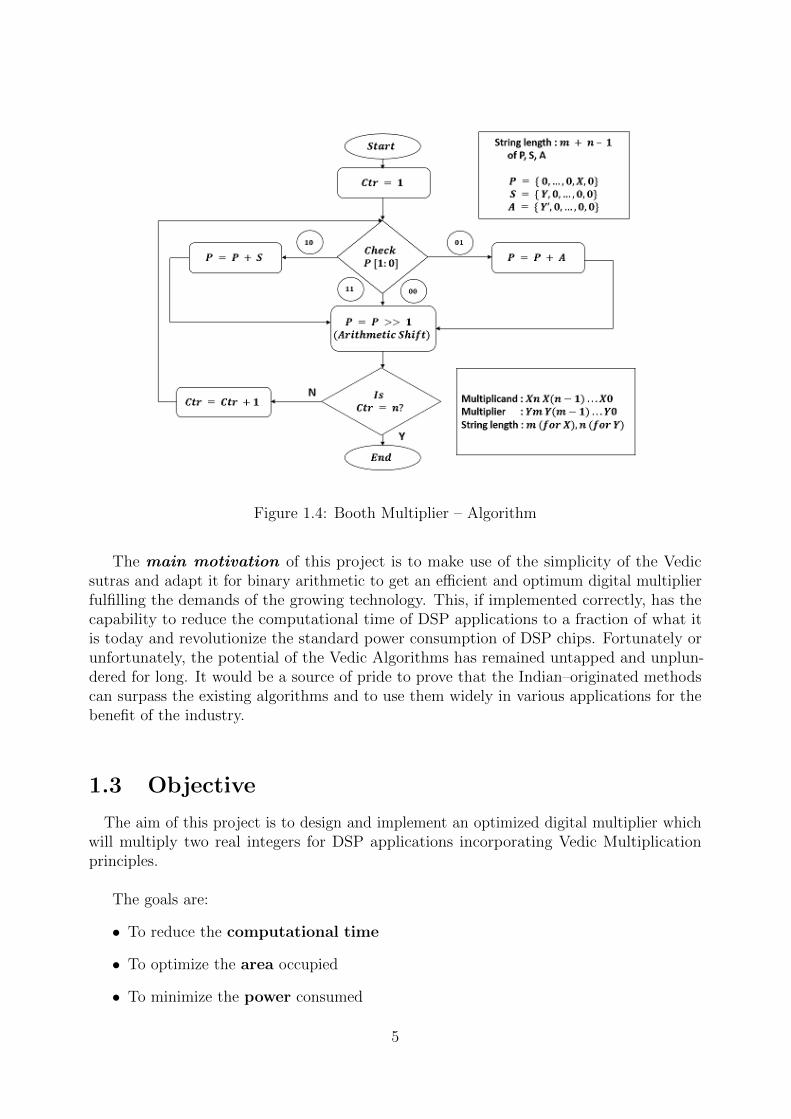
Figure 1.4: Booth Multiplier – Algorithm
The main motivation of this project is to make use of the simplicity of the Vedicsutras and adapt it for binary arithmetic to get an efficient and optimum digital multiplierfulfilling the demands of the growing technology. This, if implemented correctly, has thecapability to reduce the computational time of DSP applications to a fraction of what itis today and revolutionize the standard power consumption of DSP chips. Fortunately orunfortunately, the potential of the Vedic Algorithms has remained untapped and unplun-dered for long. It would be a source of pride to prove that the Indian–originated methodscan surpass the existing algorithms and to use them widely in various applications for thebenefit of the industry.
1.3 Objective
The aim of this project is to design and implement an optimized digital multiplier whichwill multiply two real integers for DSP applications incorporating Vedic Multiplicationprinciples.
The goals are:
• To reduce the computational time
• To optimize the area occupied
• To minimize the power consumed
5

• To realize it for 128 bits
• To develop novel algorithms for obtaining a highly optimum multiplier
• To design and implement an integrated multiplier which will decide the algorithm tobe used depending on the given inputs
• To finalize on an optimum adder and use it to implement all the addition operations
1.4 Organization of the Report
Chapter 1, the Introduction describes the need for efficient multipliers followed by abrief overview of Vedic Sutras. It illustrates the motivation behind taking up this projectand states the objectives.
Chapter 2, Literature Review, deals with all the multiplication and addition schemesreported in literature. It puts forward the concepts already proposed on related areas injournals and conferences.
Chapter 3, Theoretical Background - Algorithms presents the Vedic Multiplica-tion Algorithms – Urdhva Tiryakbhyam and Nikhilam, in detail, then proceeds with anexplanation of the Karatsuba-Ofman Algorithm and concludes by justifying the selection ofthe Carry Look Ahead (CLA) Adder.
Chapter 4, Design & Implementation, expounds on the main work done in theproject, beginning with an explanation of the modular hierarchy followed in this project,and the moving on to the actual logic employed in writing synthesizable code for eachmodule and finally concluding with an emphasis on Structural modelling as compared tobehavioural modelling.
Chapter 5, Sampoornam – the Proposed Integrated Multiplier presents a novelmultiplier designed such that the logic decides which algorithm is to be used based on theinput along with techniques employed to build this optimum, smart multiplier.
Chapter 6 gives all the Simulations and Results while Chapter 7 presents the Infer-ences of the results.
Chapter 8 is dedicated to Power Analysis, which gives a true picture of the powerconsumed in real time, based on mathematical analyses.
Finally, Chapter 9, the Conclusion completes the report by summarizing the work andconsidering the future scope .
6

Chapter 2
Literature Review
Here, a brief summary of the work that has already been done in this field with VedicMultipliers is presented. A few results are noted down for comparison later.
The implementation of an 8 − bit Vedic multiplier enhanced in terms of propagationdelay when compared with conventional multipliers like Array multiplier, Braun multiplier,Modified Booth multiplier and Wallace tree multiplier has been given by Pavan KumarU.C.S, et al, 2013. Here, they have utilized an 8− bit barrel shifter which requires only oneclock cycle for n number of shifts. The design could achieve propagation delay of 6.781 nsusing barrel shifter in base selection module and multiplier.
S. Deepak, et al, 2012, have proposed a new multiplier design which reduces the numberof partial products by 25 %. This multiplier has reported to have been used with differentadders available in literature to implement multiplier accumulator (MAC) unit and parame-ters such as propagation delay, power consumed and area occupied have been comparedin each case. From the results, Kogge Stone adder was been chosen as it was claimed tohave provided optimum values of delay and power dissipation. The results obtained havebeen compared with that of other multipliers and it has been reported that the proposedmultiplier has the lower propagation delay when compared with Array and Booth multipliers.
A high speed complex multiplier design (ASIC) using Vedic Mathematics has also beenreported by Prabir Soha, et al, 2011. A complex number multiplier design based on theformulas of the ancient Indian Vedic Mathematics, was said to have been implemented inSpice spectre and compared with the mostly used architecture like distributed arithmetic,parallel adder based implementation, and algebraic transformation based implementation.It claims to have combined the advantages of the Vedic mathematics for multiplicationwhich encounters the stages and partial product reduction. The proposed complex numbermultiplier has been reported to offer 20% and 19% improvement in terms of propagationdelay and power consumption respectively, in comparison with parallel adder based im-plementation. The corresponding improvement in terms of delay and power was reportedto be 33% and 46% respectively, with reference to the algebraic transformation basedimplementation.
Mohammed Hasmat Ali, et al, 2013, have presented a detailed study of different multipli-
7

ers based on Array Multiplier, Constant coefficient multiplication (KCM) and multiplicationbased on Vedic Mathematics. The reported multipliers have been coded in Verilog HDL(Hardware Description Language) and simulated in ModelSimXEIII6.4b and synthesized inEDA tool Xilinx ISE12. All multipliers are compared based on LUTs (Look up table) andpath delays. Results report that Vedic Urdhva Tiryakbhyam sutra is the fastest Multiplierwith least path delay. The computational path delay for proposed 8× 8 bit Vedic UrdhavaTiryakbhyam multiplier was reported to be 17.995 ns.
Karatsuba-Ofman algorithm has been reported to have been used by M.Ramalatha, etal, 2009, in the implementation of an efficient Vedic multiplier which is meant to have highspeed,less complexity and consuming less area. Also after using this multiplier module aVedic MAC unit was constructed and both these modules were integrated into an arithmeticunit along with the basic adder subtractor.
A generalized algorithm for multiplication has been reported by Ajinkya Kala, 2012,through recursive application of the Nikhilam Sutra from Vedic Mathematics, operatingin radix - 2 number system environment suitable for digital platforms. Statistical analysishas been carried out based on the number of recursions profile as a function of the smallermultiplicand. The proposed algorithm was claimed to be efficient for smaller multiplicandsas well, unlike most of the asymptotically fast algorithms. It was implemented for samesized inputs but an algorithm was presented which could be used to compute multiplicationof two variable bit numbers. The algorithm was reported to solely depend on the ratio of thenumber of 1’s and 0’s used to represent a number in binary, rather than on the magnitudeof the number. It was mentioned that as the ratio approaches 1, the number of operationsrequired for the multiplication increases and decreases as the ratio tends to move close to 0.
Ramachandran.S, et al, 2012, have thought of an Integrated Vedic multiplier architecture,which by itself selects the appropriate multiplication sutra (UT or Nikhilam) based on theinputs. So depending on inputs, whichever sutra is faster, that sutra is to be selected bythe proposed integrated Vedic multiplier architecture. It was implemented for 16 bits butthere has not been a clear report on the results or the design.
Kabiraj Sethi, et al, 2012, have proposed a high speed squaring circuit for binary numbersis proposed. High speed Vedic multiplier is used for design of the proposed squaring circuit.Only one Vedic multiplier is used instead of four multipliers as reported previously. Inaddition, one squaring circuit is used twice.
In paper presented by G.Ganesh Kumar, et al, 2012, the Verilog HDL coding of Urdhvatiryakbhyam Sutra for 32×32 bits multiplication and their FPGA implementation by XilinxSynthesis Tool on Spartan 3E kit have been done and the output has been displayed on LCDof Spartan 3E kit. The synthesis results show that the computation time for calculating theproduct of 32× 32 bits is 31.526 ns.
The designs of 16 × 16 bits, 32 × 32 bits and 64 × 64 bits Vedic multiplier havebeen implemented as reported by Vinay Kumar, 2009 on Spartan XC3S500-5-FG320 and
8

XC3S1600-5-FG484 device according to this thesis. The computation delay for 16× 16 bitsBooth multiplier was 20.09 ns and for 16× 16 bits Vedic multiplier was 6.960 ns. Alsocomputation delays for 32× 32 bits and 64× 64 bits Vedic multiplier was obtained 7.784ns and 10.241 ns respectively.
A new reduced-bit multiplication algorithm based on Vedic mathematics has beenproposed by Honey Durga Tiwari, et al, 2008. The framework of the proposed algorithmis taken from Nikhilam Sutra and is further optimized by use of some general arithmeticoperations such as expansion and bit shifting to take full advantage of bit-reduction in mul-tiplication. The computational efficiency of the algorithm has been illustrated by reducinga general 44 multiplication to a single 22 multiplication operation.
Manoranjan Pradhan, et al, 2011, have presented the concepts behind the ”UrdhvaTiryagbhyam Sutra” and ”Nikhilam Sutra” multiplication techniques in their paper. Itthen shows the architecture for a 1616 Vedic multiplier module using Urdhva TiryagbhyamSutra. The paper then extends multiplication to 1616 Vedic multiplier using ”NikhilamSutra” technique. The 1616 Vedic multiplier module using Urdhva Tiryagbhyam Sutra usesfour 88 Vedic multiplier modules; one 16− bit carry save adders, and two 17− bit full adderstages. The carry save adder in the multiplier architecture increases the speed of additionof partial products. The 1616 Vedic multiplier is reported to have been coded in VHDL,synthesized and simulated using Xilinx ISE 10.1 software. This multiplier is implementedon Spartan 2 FPGA device XC2S30-5pq208.
An integer multiplication algorithm was proposed by Shri Prakesh Dwivedi, 2013, usingNikhilam method of Vedic mathematics which can be used to multiply two binary numbersefficiently taking advantage of the fact that this sutra can convert large-digit multiplicationto corresponding small digit multiplication.
Himanshu Thapliyal, et al, 2009, have proposed parallel architectures for computingsquare and cube of a given number based on Vedic mathematics. For the Xilinx FPGAfamily, it is observed that for8− bit, the gate delay of the proposed square architecture is28 ns with area of 90(device utilized) while it is 70 ns for previously reported squares witharea of 77. For the same operand size, the gate delay in the proposed cube architecture is28 ns with area of 90 while for the cube previously reported is 79 ns with area of 768.As the operand width is increased to 16, the gate delay of the proposed square architectureincreases slightly to 38 ns with area of 348(device utilized) while for the square proposedearlier, it significantly increases to 70 ns with area of 441. For the operand size of 16, thecube statistics are found to be 54 ns with area of 1336 for the proposed Vedic cube whileit is 186 ns with area of 6550 for the cube proposed before.
9

Chapter 3
Theoretical Background – Algorithms
3.1 Urdhva Tiryakbhyam
This multiplication scheme is best understood by using an example. To illustrate, considerthe multiplication of two decimal numbers 325× 738. As shown in figure 3.1, the digits oneither side of a line are multiplied and the products from each line are added along with thecarry from the previous step. This generates one bit of the result as well as a carry. Thiscarry is added in the next step and the process goes on. In each step, the least significantbit (LSB) acts as the result bit and all other bits act as carry for the next step. Initially,the carry is taken to be zero. (Vinay Kumar, 2009 )
Figure 3.1: UT for a 3× 3 Decimal Multiplication
10

The UT algorithm is based on a novel concept through which the generation of allpartial products can be done with the concurrent addition of these partial products. Thealgorithm can be easily generalized for n× n bit multiplication due to its highly modularstructure. Since the partial products and their sums are calculated in parallel, the multiplieris independent of the clock frequency of the processor in case of a synchronous design.Thus the multiplier will require the less amount of time to calculate the product. The netadvantage is that it reduces the need of microprocessors to operate at increasingly highclock frequencies. (Vinay Kumar, 2009 )
While a higher clock frequency generally results in increased processing power, itsdisadvantage is that it also increases power dissipation which results in higher device oper-ating temperatures. By adopting the Vedic multiplier, microprocessor designers can easilycircumvent these problems to avoid catastrophic device failures. The processing power ofmultiplier can easily be increased by increasing the input and output data bus widths sinceit has a quite a regular structure. Due to this, layout can be made on a silicon chip easily.The multiplier has the advantage that as the number of bits increases, gate delay and areaincreases very slowly as compared to other multipliers. Therefore it is time, space andpower efficient. (Vinay Kumar, 2009 )
Figure 3.2: UT for a 4− bit multiplication
11

3.2 Nikhilam
Nikhilam Sutra literally means “All from 9 and last from 10”. Although it is applicableto all cases of multiplication, it is more efficient when the numbers involved are close tothe base. It finds the complement of the large number from its nearest base to perform themultiplication operation on it and thus nearer the original number to the base, lesser thecomplexity of the multiplication. This can be mathematically proven very easily as well.(Honey Durga Tiwari, et al, 2008 )
Let the two numbers be n and m. Consider a base, b.
b− n = p (3.1)
b−m = q (3.2)
n×m = (b− p) (b− q) = b2 − (p+ q) b+ pq (3.3)
n×m = b (b− p− q) + pq (3.4)
To illustrate, consider the example of multiplying 96× 93 in figure 3.3. The base is 100and hence the complements are 4 and 7 respectively. The product of the complements isgiven by 4 × 7 = 28. The common difference is given by 96 − 7 = 93 − 4 = 89. This ismultiplied with the base and added with the previous product, which turns out to be just asimple concatenation, 8928.
Figure 3.3: Nikhilam Example in Decimal Numbers
12

3.3 Karatsuba-Ofman Algorithm
The Karatsuba-Ofman algorithm is considered as one of the fastest ways to multiply longintegers. It is fundamentally useful in scaling lower bit multipliers to higher bit multipliers.It is based on the ‘Divide and Conquer’ strategy and has been proved to be asymptoticallyfaster than the standard multiplication algorithm. (M.Ramalatha, et al, 2009 )
For a 2n−bit multiplication, consider X and Y to be the the multiplicand and multiplierrespectively. Then, when XH , XL, YH and YL are n− bit numbers, we can write,
X = 2nXH +XL (3.5)
Y = 2nYH + YL (3.6)
Thus the product of X and Y can be computed as follows,
P = X.Y = (2nXH +XL).(2nYH + YL) (3.7)
Or,
P = 22n(XH .YH) + 2n(XH .YL +XL.YH) +XL.YL (3.8)
It can be observed that
XH .YL +XL.YH = (XH +XL)(YH + YL)−XH .YH −XL.YL (3.9)
i.e.,
P = 22n(XH .YH) + 2n{(XH +XL)(YH + YL)−XH .YH −XL.YL}+XL.YL (3.10)
The standard multiplication algorithm requires four n− bit multiplications. But thishas just three n− bit multiplications along with additions and subtractions as comparedto the previous four. But since each multiplication causes more delay as compared to anadder or a subtractor, this will hence result in a more optimized multiplier.
The figures 3.4 & 3.5 show the block diagram for the standard scaling multiplicationalgorithm and the Karatsuba-Ofman Algorithm respectfully.
13

Figure 3.4: Standard Scaling Multiplication Algorithm
Figure 3.5: Karatsuba-Ofman Algorithm
14

3.4 Carry Look Ahead Adder
The Carry Look Ahead (CLA) Adder generates carries before the sum is produced usingthe propagate and generate logic to make addition much faster. Thus the carry chain (thelogic that propagates the carry through the full adders of the RCA) is separated from thesum logic (the part of the full adders that produce the sum).
Figure 3.6: Partial Full Adder (PFA)
Consider a 4− bit CLA. There are two additional variables called the Generate (G) andPropagate (P ) which are fundamental for the CLA logic.
Let A and B be the two 4− bit input variables.
Gi = Ai.Bi (3.11)
Pi = Ai ⊗Bi (3.12)
C1 = G0 + P0.C0 (3.13)
C2 = G1 + P1.C1 = G1 + P1.G0 + P1.P0.C0 (3.14)
C3 = G2 + P2.C2 = G2 + P2.G1 + P2.P1.G0 + P2.P1.P0.C0 (3.15)
C4 = G3 + P3.C3 = G3 + P3.G2 + P3.P2.G1 + P3.P2.P1.G0 + P3.P2.P1.P0.C0 (3.16)
Si = Pi ⊗ Ci (3.17)
GG = G3 + P3.G2 + P3.P2.G1 + P3.P2.P1.G0 (3.18)
PG = P3.P2.P1.P0 (3.19)
These equations show that every carryout in the adder can be determined with just theinput operands and initial carryin (C0). The size of a CLA adder block is chosen as 4 bits.An 8− bit CLA can be built from two 4− bit CLA blocks, a 16− bit CLA from four whilea 32− bit CLA can be built from two 16− bit CLA blocks and so on with the help of theGroup Generate (GG) and Group Propagate (PG) pins.
15

Figure 3.7: 4− bit CLA
Figure 3.8: 16− bit CLA adder from 4− bit CLA adders
16

Critical Path Determination
Assuming that all gate delays are the same, the delay for a 4− bit CLA adder includesone gate delay to calculate the propagate and generate signals, two gate delays to calculatecarry signals, and one gate delay to calculate the sum signals; i.e four gate delays. (MichaelAndrew Lai, 2002 )
For a 16 − bit CLA adder there is one gate delay to calculate the propagate andgenerate signal (from the PFA), two gate delays to calculate the group propagate andgenerate in the first level of carry logic, two gate delays for the carryout signals in thesecond level of carry logic, and one gate delay for the sum signals. The second level of carrylogic for the 16− bit CLA adder contributes an additional two gate delays over the 4− bitCLA adder, thus increasing the total to six gate delays. Hence,
CLA levels (groupsize = 4) = log4N (3.20)
CLA levels (groupsize = k) = logkN (3.21)
CLA gate delay = 2 + 2.log4N (3.22)
Figure 3.9: Critical Path of a 16− bit CLA
In table 3.1, the delay of a CLA adder is logarithmically dependent on the size ofthe adder which theoretically results in one of the fastest adder architectures. And it has theregularity that will allow size adjustment of the adder without much additional design time.It is for these reasons that the CLA architecture is chosen as the adder after comparisonwith the Ripple Carry Adder (RCA), the Carry Skip Adder (CSKA) and the Linear CarrySelect Adder (CSLA). Power consumption of the CLA might be slightly higher as comparedto Kogge-Stone Adders, etc but the ease of scaling higher bit adders, the lower area andthe lesser delay make this trade-off very slight. (Michael Andrew Lai, 2002 )
17

Table 3.1: Adder Comparison – N : input size, k: group size
Adder Delay Normalized Area Normalized Design Time
RCA N 1 1CSKA N/k 1.14 2CLA logkN 1.88 8
CSLA logkN(N/k)
2.56 10
The Delay column expresses how the delay of the adder is proportional to the length(input size). The next column, Area, normalizes the area for the RCA (based on the subcells)and compares the relative sizes of the other adders to this normalized value. And finally, theDesign Time column is an estimate of the normalized time required to design the particularadder based on the RCA design time. (Michael Andrew Lai, 2002 )
18

Chapter 4
Design & Implementation
4.1 Synthesizable Code for Hardware Efficiency
The process of automatically converting the description in RTL to gates from the targettechnology is called Synthesis . It converts the design from a higher level description to alower one. Normal programming and HDL (Hardware Description Language) programmingare usually built over the same platform C. But both are fundamentally different. HDL’s(eg. Verilog) are aimed at both simulation and synthesis of digital circuits. All descriptionscan be simulated, but only some can be synthesized. And by changing the method of coding,the synthesized design can be made optimum.
Figure 4.1: Structural Programming
Verilog has two major programming models - Behavioural and Structural, the formermore useful for simulations and the latter for hardware level. However, structural mode ismore time consuming and requires more effort. An overall plan is required for implementingstructural codes. Developing code as the project progresses will not yield optimal results.But for making the codes truly synthesizable as well as for true hardware optimization,structural programming is a must.
19

Here, the design of each of the modules along with its implementation using variousoptimization methods and logical techniques is presented. Also, several new designs andoriginal combinations of existing designs have also been implemented in order to increasethe efficiency.
4.2 Vedic UT
The basic unit of the 128− bit multiplier is the 4− bit Vedic multiplier built using theUrdhva Tiryakbhyam logic which was explained for decimal numbers in the previous chapter.
Consider the inputs to be the 4− bit numbers A[3 : 0] and B[3 : 0].
A[3 : 0] = a3a2a1a0 (4.1)
B[3 : 0] = b3b2b1b0 (4.2)
Then we have,
c0p0 = a0b0 (4.3)
c1p1 = a1b0 + a0b1 + c0 (4.4)
c2p2 = a2b0 + a1b1 + a0b2 + c1 (4.5)
c3p3 = a3b0 + a2b1 + a1b2 + a0b3 + c2 (4.6)
c4p4 = a3b1 + a2b2 + a1b3 + c3 (4.7)
c5p5 = a3b2 + a2b3 + c4 (4.8)
c6p6 = a3b3 + c5 (4.9)
Here, the ci’s can be multi-bit numbers while the pi’s are single-bit numbers. Theadditions are performed using CLA adders as mentioned before. The code is optimized forsynthesis with power and delay in consideration. Higher order UT blocks are built accordingto the proposed scaling plan mentioned below.
4.3 Scaling – The overall plan
Figure 4.2: Multiplication of two 2n− bit numbers
20

An n− bit multiplier is used to build a 2n− bit multiplier. This uses the Karatsuba-Ofman Algorithm mentioned before, as well as innovative logic and coding techniques formaximum efficiency. After this is implemented, 8−bit, 16−bit, 32−bit, 64−bit and 128−bitmultipliers can easily be built by substituting n = 4, 8, 16, 32 and 64 respectively startingwith the basic 4− bit UT multiplier as the building block. The n− bit additions are doneusing n− bit CLA’s.
The scaling up procedure is as follows:
Given:
A[(n− 1) : 0]×B[(n− 1) : 0]→ Prod[(2n− 1) : 0] n-bit multiplier
To build:
A[(2n− 1) : 0]×B[(2n− 1) : 0]→ Prod[(4n− 1) : 0] 2n-bit multiplier
The input operands are split into higher order and lower order terms as shown.
AH [(n− 1) : 0] = A [(2n− 1) : n] (4.10)
AL [(n− 1) : 0] = A [(n− 1) : 0] (4.11)
BH [(n− 1) : 0] = B [(2n− 1) : n] (4.12)
BL [(n− 1) : 0] = B [(n− 1) : 0] (4.13)
X = AH ×BH (4.14)
Y = AL×BL (4.15)
P = X + Y (4.16)
Z1 = AH + AL (4.17)
Z2 = BH +BL (4.18)
T1 = Z1 [(n− 1) : 0]× Z2 [(n− 1) : 0] (4.19)
T2 = Z1 [(n− 1) : 0] << n.Z2 [n] (4.20)
T3 = Z2 [(n− 1) : 0] << n.Z1 [n] (4.21)
TX = T1 + T2 (4.22)
TY = TX + T3 (4.23)
x = Z1[n] . Z2[n] (4.24)
y = x+ TX [2n] + TY [2n] (4.25)
Z = {y, TY } (4.26)
R = Z + P + 1 (4.27)
Prod = {X, Y }+ (R << n) (4.28)
21

4.3.1 Where have the optimizations taken place?
1. A more efficient 4− bit Vedic Multiplier is developed in structural modelling
2. The faster and efficient CLA adder is used throughout
3. The traditional behavioural left shift operator (<<) is replaced with AND logic
4. (2n+ 1)− bit addition (which will have to be done by a 4n− bit adder) is convertedto a 2n− bit addition and a single bit addition (Full adder)
5. An efficient combiner logic is developed which requires only one addition and aconcatenation
4.4 UT Squaring
It can be seen easily that a special case of multiplication, i.e. Squaring, is much simplerin terms of hardware and software design as compared to the normal situations. This canbe exploited to build the integrated multiplier.
For squaring a 4− bit number, i.e A[3 : 0] = B[3 : 0]
c0p0 = a0 (4.29)
c1p1 = 2.a1a0 + c0 (4.30)
c2p2 = 2.a2a0 + a1a1 + c1 (4.31)
c3p3 = 2.a3a0 + 2.a2a1 + c2 (4.32)
c4p4 = 2.a3a1 + a2a2 + c3 (4.33)
c5p5 = 2.a3a2 + c4 (4.34)
c6p6 = a3a3 + c5 (4.35)
Thus, since multiplication by 2 is just a left shift by 1 bit, the square is a very specialcase that is easy to implement and which consumes less area, power and delay as comparedto the normal Vedic multiplier.
4.4.1 Scaling – Adapted for Squares
Figure 4.3: 2n− bit Squaring Unit
22

Building a 2n − bit squaring unit from an n − bit squaring unit is much easier thanbuilding a 2n− bit multiplier from an n− bit multiplier.
AH [(n− 1) : 0] = A [(2n− 1) : n] (4.36)
AL [(n− 1) : 0] = A [(n− 1) : 0] (4.37)
X = AH2 (4.38)
Y = AL2 (4.39)
Z = 2 (AH × AL) (4.40)
Prod = {X, Y }+ (Z << n) (4.41)
As can be seen, the 15 steps in scaling the normal UT multiplier have been reduced tojust 4 for scaling the UT square. Again, the multiplication by 2 is just a left shift by 1 bitas mentioned before.
4.5 Proposed Design D
Given two operands A and B, assuming without loss of generality, A > B, it can beobserved that,
A×B =4.AB
4(4.42)
=(A+B)2 − (A−B)2
4(4.43)
=(A+B
2
)2
−(A−B
2
)2
(4.44)
=(A+B
2
)2
−(A+B
2−B
)2
(4.45)
(4.46)
Thus,A×B = (av)2 − (dev)2 (4.47)
A multiplication is broken down into the difference between two squares. Since onlyintegers are being dealt with here, this would work only when the operands are both evenor both odd. Otherwise the average would turn out to be a floating point.
Squaring is less costly in power expenditure, area occupancy and delay. This designtakes advantage of this fact and makes it possible for it to be used for non-square integerstoo.
23

4.6 Thresholding Nikhilam
Here the basic idea of Nikhilam is extended to binary. Since Nikhilam is efficient when theinputs are very near to the base, a threshold is chosen, upto which we can consider Nikhilamto be better. It is estimated that the most optimum threshold would be (1/4)th the input size.
For a 16 − bit multiplier, a possible threshold can be 4 bits. This means that if thedifference between the base and number comes out to be a 4− bit integer, then Nikhilam isconsidered better. For the multiplication of the 4− bit complements, the already optimized4− bit Vedic Multiplier will be used. Thus, a 16− bit multiplication will be reduced to a4− bit multiplication along with addition & subtraction.
Table 4.1: Thresholds for various multipliers
Input size Threshold Value
8 bits 2 bits16 bits 4 bits32 bits 8 bits64 bits 16 bits128 bits 32 bits
Range of Inputs
Since Nikhilam is efficient for a certain range of inputs, it should be determined if thegiven inputs belong to that range.
Given the size of the input as is and the threshold size as ts, we can find the range ofvalues that can be used effectively with Nikhilam, range, as follows. Base, B = 2(is−1) andthreshold value, Th = 2ts − 1
range ε [B − Th,B + Th] (4.48)
Consider the input to be m and n, and the base, b.
Case 1: Both inputs are greater than the base
Table 4.2: Multiplication of m× n, base r
Integer Base difference
Multiplicand m m− r = aMultiplier n n− r = b
m+ n− r a× bResult r(m+ n− r) + ab
24

Case 2: Both inputs are less than the base
Table 4.3: Multiplication of m× n, base r
Integer Base difference
Multiplicand m r −m = aMultiplier n r − n = b
r −m− n a× bResult r(r −m− n) + ab
Case 3: One input (m) is greater than the base & the other (n), less
Table 4.4: Multiplication of m× n, base r
Integer Base difference
Multiplicand m m− r = aMultiplier n [n− r = b = −q]→ [r − n = q]
m+ n− r a× (−q)Result r(m+ n− r)− aq
Steps to be followed
1. Choose base r for the inputs m and n
2. Decide if the inputs belong to the correct range of inputs for Nikhilam
3. Decide which case of Thresholding Nikhilam to use
Optimization Points
1. Base can always be chosen as 2(is−1) for optimum performance.
2. The adders used are CLA adders.
3. A higher order multiplication is reduced to a few addition operations and a lowerorder multiplication.
4.7 Successive Nikhilam
Instead of applying Nikhilam only for a select few numbers as given by the threshold,we can use it for all integers by applying it successively. In this case, the entire process ofmultiplication is broken down into addition and subtraction.
25

Table 4.5: Nikhilam – 1111× 1111, base = 1000
Bits Base Difference Next Difference Next Difference
m = 1111 1111− 1000 = 111 111− 100 = 11 11− 10 = 1n = 1111 1111− 1000 = 111 111− 100 = 11 11− 10 = 1
1× 1 = 110(11 + 1) + 1 = x1
100(111 + 11) + x1 = x21000(1111 + 111) + x2 = x3
Ans = 11100001
Consider the example in table 4.5 – 1111× 1111. This has reduced to just one AND(1− bit) operation, additions and shifting (multiplying by the base is basically left-shifting).To account for multiplications which involve different sizes, a little more thought has to begiven. The final algorithm designed is as given below.
Given is− bit inputs, m and n
p = m⊗ n (4.49)
q = m⊗ (is)′b0 (4.50)
S0 = m[0]× n[0] (4.51)
for −→ i = 1 : (is− 1) (4.52)
case(p[i], q[i]) (4.53)
00 → Si = 0 (4.54)
01 → Si = m[i : 0] + n[(i− 1) : 0] (4.55)
10 → Si = m[(i− 1) : 0] (4.56)
11 → Si = n[(i− 1) : 0] (4.57)
endcase (4.58)
m× n =(is−1)∑i=0
Si (4.59)
Optimization Points
1. Since only one 1− bit AND operation is required along with aditions and shiftings, asthe input size increases, Successive Nikhilam will grow more efficient.
2. One disadvantage is for an n− bit input, it requires n steps.
3. This is basically recursion. Hence implementing it in Structural Modelling is moredifficult and it can prove costly in terms of power and delay.
26

Since addition is performed using CLA’s, for an n− bit multiplier,
Table 4.6: Total No. of Adders Required – Successive Nikhilam
CLA Type # required
CLA(2n) n/2CLA(n) n/2CLA(n/2) n/4
. .
. .CLA(2) 1
Because the number of adders can be predetermined for a multiplier based on its inputsize, it is very easy to give a nearly estimate of the power consumption and the area occupied,given the details of the adders. More than any other multiplier, Successive Nikhilam almostsolely depends on the adders since the only multiplication that takes place is a 1− bit ANDoperation.
27

Chapter 5
Sampoornam – the ProposedIntegrated Multiplier
A novel multiplier, which will integrate maximum of the advantages in each designimplemented in the above chapter, is proposed. It is designed to have a specialized logic unitthat will decide which multiplier is to be used for optimum results of all the given choices,based on the input values. This will be a thorough multiplier with no human interventionrequired. Since it is meant to be absolute and completely based on Vedic roots, it would beapt to name it as “Sampoornam” or the “Absolute Vedic” multiplier.
5.1 Sampoornam: Specifications
There are around 7 possible designs to choose from, as proposed in this report, in orderto multiply two given integers, apart from the case when one of the inputs is a 0 (Output 0).
They are:
1. Vedic multiplier based solely on Urdhva Tiryakbhyam – Vedic UT
2. Proposed design D for multiplication derived from squaring logic – Design D
3. Nikhilam multiplier with both inputs above the base – Nikh GG
4. Nikhilam multiplier with both inputs below the base – Nikh SS
5. Nikhilam multiplier with one input above and one below – Nikh SG
6. Squaring logic based on Urdhva Tiryakbhyam – UT Square
7. When either of the numbers is equal to the base – Left Shift
The Successive Nikhilam is not a good candidate for integrating into the Sampoornammultiplier since it is based on recursion while rest of the blocks are not. And the powerconsumed, area occupied and the delay will be more than normal if it is to be included. Sothe only possible options are those listed above. Henceforth in this report, Nikhilam refersto Thresholding Nikhilam unless otherwise specified.
28

5.2 Sampoornam: Logic
Consider the inputs to be x and y, with the base as b. Let t be the threshold value forNikhilam.
Table 5.1: Designs and their input constraints
Design Input Constraints
Left Shift x or y = bUT Square x = yNikh SG x ε (b, b+ t) and y ε (b− t, t)Nikh GG x, y ε (b, b+ t)Nikh SS x, y ε (b− t, b)Design D x− y = 2k, k is an integerOutput 0 x or y = 0
However, on performing the analyses, as will be seen in the Chapter 6, it is found thatDesign D implemented with CLA Adder comes to be less optimum than the Vedic UTmultiplier. For this reason, the Design D is not included in the final integrated multiplier –Sampoornam . Other inferences about this will be pointed out in Chapter 7.
Figure 5.1: Sampoornam Logic – Flowchart
29

5.3 Sampoornam: Implementation
Figure 5.2: Sampoornam – Implementation
The code is implemented according to the algorithm given above. A point to be noted isthat, this is implemented completely using Combinational Logic Gates along with compara-tors. This could have been very simply written as a set of if conditions, which would givethe same output. However, then the logic block will not be optimum and will tend to drawmore power, as well as occupy more area. This is so designed in order to be in accordancewith Structural Programming.
Table 5.2: Priority Encoder – Output
S2S1S0 Design Selected
111 Left Shift y110 Left Shift x101 UT Square100 Nikh SG011 Nikh SS010 Nikh GG001 Vedic UT000 Output 0
30

5.4 Sampoornam: Advantages
1. Only one of the designed modules will be ON at any given time. Hence, the powerdrawn overall will be split among them.
2. The Logic block (which decides which module will be ON) is completely separatedfrom the modules. That is, the modules and the logic block can be independentlyoptimized.
3. Since some modules are very highly optimum for a given range of inputs, using themonly for those inputs is going to increase the overall efficiency of the multiplier.
4. This multiplier is easily hardware realizable as well, having proper modularity andstructure. Multiplexers can be employed instead of the Priority Encoder in certainsituations.
5. No manual intervention is required during any step for implementing the logic.
It is hoped that the Sampoorna Multiplier will be truly complete and absolute. Theresults of various analyses that was done on it is given in the following chapters.
31

Chapter 6
Simulations and Results
The code is written in Verilog HDL using the Xilinx ISE 14.3 Design Suite. Test benchesare written to validate the codes. Then the codes are fed to the Cadence Encounter RCCompiler, i.e RTL Compiler and the parameters and paths are specified to perform thepower analysis, to determine the area occupancy and the worst path delay for each module.
6.1 Vedic UT
6.1.1 RTL Schematics
Figure 6.1: 2− bit Vedic UT
Figure 6.2: 4− bit Vedic UT
32

Figure 6.3: 8− bit Vedic UT
Figure 6.4: 16− bit Vedic UT
33

Figure 6.5: 32− bit Vedic UT
Figure 6.6: 64− bit Vedic UT
34

Figure 6.7: 128− bit Vedic UT
35

6.1.2 RTL Results
Table 6.1: Vedic UT
# bits Area(nm2) Power(nW) Delay(ps)
2 10 954.171 62.84 71 7782.601 3408 454 63223.888 814.9016 1913 360307.407 1500.2032 6909 1688282.769 2321.5064 23346 7212137.495 3522.10128 75013 28739302.317 4970.80
6.2 Vedic Square
6.2.1 RTL Schematics
Figure 6.8: 2− bit Vedic Square
Figure 6.9: 4− bit Vedic Square
36

Figure 6.10: 8− bit Vedic Square
Figure 6.11: 16− bit Vedic Square
37

6.2.2 RTL Results
Table 6.2: Vedic Square
# bits Area(nm2) Power(nW) Delay(ps)
2 4 378.573 39.24 35 3285.703 240.38 187 19757.673 51816 943 119473.143 1029.1032 4049 663927.624 179164 15542 3231041.100 2615.60128 55720 14399463.453 3933.2
6.3 Design D
6.3.1 RTL Results
Table 6.3: Design D
# bits Area(nm2) Power(nW) Delay(ps)
8 527 77934.629 787.2016 2259 445024.996 1446.8032 8944 23973.226 2343.4064 32880 109168939.094 3336.30128 115260 47426654.289 4811.20
6.4 Nikhilam GG
6.4.1 RTL Schematics
Figure 6.12: 8− bit Nikh GG
38

Figure 6.13: 16− bit Nikh GG
Figure 6.14: 32− bit Nikh GG
Figure 6.15: 64− bit Nikh GG
39

6.4.2 RTL Results
Table 6.4: Nikh GG
# bits Area(nm2) Power(nW) Delay(ps)
8 18 1663.124 62.816 87 9331.961 34032 497 68958.150 814.9064 2011 370320.247 1500.2128 7121 1738297.467 2326.70
6.5 Nikhilam - SG
6.5.1 RTL Schematics
Figure 6.16: 8− bit Nikh SG
.
.
40

Figure 6.17: 16− bit Nikh SG
Figure 6.18: 32− bit Nikh SG
41

6.5.2 RTL Results
Table 6.5: Nikh SG
# bits Area(nm2) Power(nW) Delay(ps)
8 52 4700.96 262.4016 155 16786.435 590.4032 635 80516.342 1185.0064 2276 396173.188 1968.90128 7649 1706659.996 2915.60
6.6 Nikhilam SS
6.6.1 RTL Schematics
Figure 6.19: 8− bit Nikh SS
Figure 6.20: 16− bit Nikh SS
.
42

Figure 6.21: 32− bit Nikh SS
.
.
.
6.6.2 RTL Results
Table 6.6: Nikh SS
# bits Area(nm2) Power(nW) Delay(ps)
8 28 2739.485 144.1016 122 13466.568 40832 575 81261.636 960.1064 2174 379401.386 1691.20128 7452 1760731.869 2577.60
.
.
43

6.7 Logic Block
6.7.1 RTL Schematics
Figure 6.22: 8− bit Nikh SS
6.7.2 RTL Results
Table 6.7: Logic
# bits Area(nm2) Power(nW) Delay(ps)
8 51 3605.177 190.6016 88 5701.256 209.5032 165 9414.358 367.3064 307 17494.020 382.40128 608 33077.098 775.50
44
6.8 CLA Blocks
6.8.1 RTL Analysis
Table 6.8: CLA Analysis
CLA Area(nm2) Power(nW) Delay(ps)
cla2 10 1222.249 76cla4 27 2740.212 112cla8 82 7792.435 189cla16 115 12547.3 252cla32 232 26374.588 359cla64 464 50265.548 407cla128 938 104861.319 511cla256 1882 210065.503 568
6.9 Test Bench Output
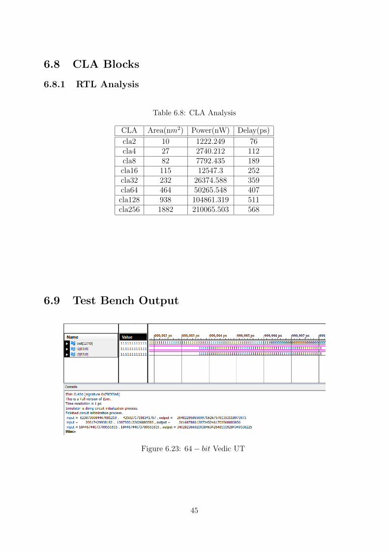
Figure 6.23: 64− bit Vedic UT
45

Figure 6.24: 128− bit Vedic UT
46

Chapter 7
Inferences
The schematics and the RTL results for each of the blocks were given in the previouschapter. However, just the results alone are insufficient to gain a complete understandingof the project. Rather, knowing what blocks/what codes/what logic caused these resultsand how they caused the results to come, can help us to evaluate it as well as predict theoutcomes for optimization if the project is expanded to a higher scale in the future.
Not only this, but a complete analysis of the results can be made only by comparing eachblock with the other as well as comparing with the existing literature. These comparisonscan yield insight into knowing which module would be most optimum in which situation aswell as for estimating the efficiency and the drawbacks.
7.1 Comparison –
Vedic UT, Vedic Square & Design D
Power Consumption
Figure 7.1: Power Consumption in nW
47

Area occupancy
Figure 7.2: Area occupied in nm2
Delay
Figure 7.3: Worst Path Delay in ps
It is clear that the Vedic Square is the most optimum – having a clean, almost lineargraph with a very low slope. It is not surprising too that values increase less rapidly withthe increase in number of bits as compared to the other two, for after all, the input size isjust a fraction of what it is for the rest.
It is observed that the increase is more for Design D in both Area and Power as comparedto Vedic UT when the number of bits increases. However, for the Delay, it is seen thatDesign D is slightly better than Vedic UT. Thus it is more advisable to go for Design Donly when the speed is of primary importance and power dissipation and area occupancyare of no concern. Then, better delay will be obtained, however slight it may be.
48

7.2 A look at the 3 cases of Nikhilam
With the power given in nW, Area in nm2 and the delay in ps.
Figure 7.4: Comparison between the 3 cases of Nikhilam
All the 3 cases of Nikhilam have almost the same Power Consumption curve. The Areacurves are slightly different while maximum variance can be observed in the Delay curves.When both the inputs are larger than the base with the Nikhilam threshold (Nikhilam GG),the delay is the least, followed by Nikhilam SS which requires both the inputs to be belowthe base within the said threshold. Nikhilam SG which deals with one input being largerand the other being smaller than the base has the maximum delay associated with it. Thiscan be put to use in application specific design of multipliers.
Another important fact the graphs of Nikhilam yield is that all the 3 cases have thesame power, more or less. This has a huge impact while doing the power analysis, sinceall the 3 cases can be considered as one and need not be dealt as separate cases. This willsimplify the power analysis tremendously.
49

7.3 Analytical Comparisons with the Vedic UT
Table 7.1: Vedic UT to Vedic Square: % reduction
# bits Power(%) Area(%) Delay(%)
2 60.3 60 37.64 58.1 50.7 29.48 68.8 58.8 36.416 66.8 50.7 36.432 60.7 41.4 22.964 55.2 33.4 25.7128 49.9 25.7 20.9
Table 7.2: Vedic UT to Design D: % reduction
# bits Power(%) Area(%) Delay(%)
8 -23.2 -16.1 4.316 -23.5 -18.1 3.632 -42.0 -29.5 -0.964 -51.4 -40.8 5.3128 -65.0 -53.7 3.2
Table 7.3: Vedic UT to Nikhilam (maximum): % reduction
# bits Power(%) Area(%) Delay(%)
8 92.6 88.5 67.816 735.3 91.9 60.632 95.2 91.9 60.664 94.5 90.3 49.0128 94.0 89.8 41.3
The above tables indicate the exact percentage of improvement of the designs from theVedic UT. Since the values of Design D are negative, it can be inferred that
The performance of
Nikhilam > V edic Square > V edic UT > Design D
50

7.4 Analysis of the Logic Block and CLA Adder
7.4.1 Logic Block
Figure 7.5: Logic Modules – Variation of Parameters
As can be seen, there is a linear relationship between the Power and number of bitsas well as between the area and number of bits. The delay is almost linear with just oneoutlier. This fact can be used for estimating the values for larger logic blocks.
This linearity probably comes from the fact that all the logic blocks have the samedependence on comparators and the comparators are built linearly.
7.4.2 CLA Adder
Another block that shows linearity is the CLA adder.
51

Figure 7.6: CLA Adder – Variation of Parameters
The power and area again follow a linear relationship with the number of bits while thedelay is completely non-linear. This should not be surprising as we proved that CLA adderhas a logarithmically growing delay. Hence, for lower power applications of the multiplier,some other adder should be chosen but for most of its part, the CLA is an excellent choice.
52

Chapter 8
Comparison with Existing Work
On comparison with other reported multipliers, it is seen that even the Vedic UT, themaximum valued block in Sampoornam is more efficient. Hence, it can be concluded thatthe Sampoornam multiplier is very efficient.
Table 8.1: As reported in Literature
# bits Power(uW) Area(nm2) Delay(ps) Reference
8 2342 13555 2342 Proposed Design [19]8 2654 22674 2816 Array [19]8 1688 12374 2632 Booth [19]8 - - 17995 Vedic [13]8 - - 15416 Vedic [14]16 - - 22604 Vedic [14]32 - - 35760 Vedic [14]64 - - 44870 Vedic [14]8 - - 18699 Nikhilam [17]16 - - 20094 Nikhilam [17]32 - - 24075 Nikhilam [17]64 - - 32816 Nikhilam [17]8 168000 - 26825 Array [4]8 99000 - 23079 UT [4]8 148000 - 27878 Nikh [4]16 250000 - 53276 Array [4]16 118000 - 41350 UT [4]16 118000 - 51323 Nikh [4]32 382000 - 107128 Array [4]32 315000 - 72332 UT [4]32 315000 - 90747 Nikh [4]
- −→ Data not given.
53

Table 8.2: Vedic UT
# bits Area(nm2) Power(uW) Delay(ps)
2 10 0.954171 62.84 71 7.782601 3408 454 63.223888 814.9016 1913 360.307407 1500.2032 6909 1688.282769 2321.5064 23346 7212.137495 3522.10128 75013 28739.302317 4970.80
As can be seen from the tables, the Vedic UT (and hence the Sampoornam) multiplierare more efficient than those reported in the literature.
With the 21 multipliers compared here, only one 64− bit bit multiplier is reported. Itsdelay, 32.82 ns is even more than the 128− bit Vedic UT’s delay of 4.97 ns. That is almosta 84.72% reduction for a higher order multiplier. Similarly, there’s a steep change from theexisting multipliers to the proposed multiplier.
Thus we can conclude that the multipliers designed in this report are more optimumthan the current multipliers.
54

Chapter 9
Power Analysis
The disadvantage with performing the power analysis in software, like Cadence here, isthat they won’t give accurate results as will occur in real life in a few cases. One such case iswhen many submodules are present but only one of them should be ON at a time based onindividual ENABLE pins dependent on the input values. Since conditional instantiationof a module is not possible in Verilog, the power as calculated by the software will invariablyassume all the submodules are ON at the same time and thus give an exorbitantly high value.
However, this is an inaccurate result. The Sampoornam multiplier precisely fallsunder the above category. And power analysis is a must for Sampoornam in order tojudge its performance.
A novel method of analysis is proposed based on mathematical principles of probability.Since the multiplier is now input dependent, consider the following mathematical modelpresented below.
Let the submodules be A1, A2, . . . , Am with power as given below.
Table 9.1: Submodules & their Power consumption
Module Power
A1 P1
A2 P2
. .
. .Ai Pi
. .
. .Am Pm
55

Let the range of inputs for the module be denoted by range = [p, q] and let
|range| = R (9.1)
Let the inputs be denoted by x, y.
Let the range (set of inputs for which the submodule should be ON) of each submoduleAi be given by Si.
And let pi be the probability that x, y ∈ Si.
Note,S1 ∪ S2 . . . ∪ Sm = range (9.2)
m∑i=1
pi = 1 (9.3)
Now the actual power dissipated contributed by the submodules can be found by
Pmod =m∑i=1
pi.Pi (9.4)
= p1.P1 + p2.P2 + . . .+ pm.Pm (9.5)
Adding the power dissipated by the logic block, we get
Pnet = Pmod + Plogic
9.1 Power analysis – Sampoornam
Considering the 3 cases of Nikhilam as one, since their power consumption is almost thesame, we have the modules as Vedic UT, Nikhilam and Vedic Square (say). If Design D,Left Shift, or any other modules are to be added, they can be done by following the samesteps as shown below.
Table 9.2: Submodules – Sampoornam
Module Power
A1 Vedic SquareA2 NikhilamA3 Vedic UT
56

Let the inputs be n− bit in size. Let the threshold size be k bits.
Probabilities that the inputs belong to a module are given by,
p1 = prob (inputs ∈ Vedic Square set)
p2 = prob (inputs ∈ Nikhilam set)
p3 = prob (inputs ∈ Vedic UT set)
For Vedic Square, to find the probability when the inputs are to be equal, consider thatyou are selecting out out of 2n first. The probability of doing so is 1. Now the probability ofpicking the same number chosen before again implies now the choices are just one number,i.e, that which was picked before. So, the probability is given by
p1 = 1.1
2n=
1
2n(9.6)
For Nikhilam, the number of favourable outcomes is given by 2(2k − 1) for one input.The total number of outcomes are 2n. So the probability is given by,
p2 =
(2(2k − 1)
2n
)2
=
(2k − 1
22n−1
)2
(9.7)
For Vedic UT, finding probability is easy. From eq (8.3), it is given by
p3 = 1− p1 − p2 (9.8)
After this, the parameters are substituted in eq (8.4) and Pnet is then calculated byadding Plogic
For a 16−bitmultiplier, the value comes to 366004.256 nW as compared to 502273.461
nW given by Cadence RTL analysis.
57

Chapter 10
Conclusion
A 128− bit digital multiplier is built stage by stage starting with a 2− bit and a 4− bitmultiplier. The Vedic algorithms – Urdhva Tiryakbyam and Nikhilam are effectively utilizedin order to increase its efficiency. Along with the Vedic principles, the Karatsuba-Ofmanalgorithm is implemented to scale a higher order multiplier from a lower order multiplier.
Many designs based on known Vedic algorithms for decimal numbers are adapted fordigital systems and implemented with many innovations. To summarize, the major designsare the Vedic UT – based purely on the Urdhva Tiryakbyam, Vedic Square – whichexploits the ease of squaring digital numerbs using Vedic principles, the ThresholdingNikhilam which uses the Nikhilam algorithm with a threshold, the Successive Nikhilamwhich recursively uses Nikhilam to reduce the multiplication to just a 1− bit AND operationand Design D – which is based on a famous algebraic manipulation.
A unique integrated multiplier – the Sampoornam multiplier is proposed and a sepa-rate logic block is built to make use of all the modules mentioned above. These variousdesigns proposed above are most optimum for a specific set of inputs particularly. Thishas been incorporated into Sampoornam in order to make it a complete multiplier. Thefeatures of Sampoornam include the presence of a logic block to determine which designis to be used for a given set of inputs along with well optimized multiplier designs whichmakes it unique.
Each module of the integrated multiplier is compared with other modules designed aswell those reported in literature. A detailed analysis has been done and parameters suchas time delay, power dissipation and area occupied are found for each case. These arecompared with the existing multipliers and the proposed multiplier is found to be moreoptimum than many of the existing multipliers.
58

10.1 Future Scope
The multiplier can be made more optimum by using different adders apart from the oneproposed using CLA. This is possible because of its modularity. Each multiplier modulecan be made more optimum by designing a more efficient adder since almost every blockdepends on an adder. Better designed comparators can also highly optimize the integratedmultiplier since the Logic unit makes use of comparators.
The multiplier can be extended for signed numbers (which just involves an XOR op-eration of the MSBs) as well as for floating point numbers. Globally synchronous, locallyasynchronous or globally asynchronous, locally synchronous MAC units can be developedusing this multiplier.
This multiplier can be fabricated after making the layout. Also, the results obtainedfrom the RTL analysis can be made better by using more updated technology like 90nm processes. Like in ASIC design, the multiplier can be customized for each constraintcriterion with respect to specific applications.
There is always a huge demand for an optimized multiplier in the industry and it is trulyamazing to see that the ancient centuries-old Vedic principles can be used to satisfy thepresent day demands. More research should be done to uncover these hidden facts whichcan reshape our future completely.
59

Bibliography
[1] Ajinkya Kale, Shaunak Vaidya, Ashish Joglekar, A Generalized Recursive Algorithmfor Binary Multiplication based on Vedic Mathematics
[2] Devika Jaina, Kabiraj Sethi, Rutuparna Panda, Vedic Mathematics based MultiplyAccumulate Unit, 2011 International Conference on Computational Intelligence andCommunication Systems
[3] G.Ganesh Kumar, V.Charishma, Design of High Speed Vedic Multiplier using VedicMathematics Techniques, International Journal of Scientific and Research Publications,Volume 2, Issue 3, March 2012
[4] Harish Kumar, Implementation and Analysis of power, area and delay of Array, Urdhvaand Nikhilam Vedic Multipliers, International Journal of Scientific and ResearchPublications, Volume 3, Issue 1, January 2013
[5] Harpreet Singh Dhillon and Abhijit Mitra, A Reduced-Bit Multiplication Algorithmfor Digital Arithmetic, World Academy of Science, Engineering and Technology 19,2008
[6] Himanshu Thapliyal, Saurabh Kotiyal* and M.B Srinivas, Design and Analysis ofA Novel Parallel Square and Cube Architecture Based On Ancient Indian VedicMathematics
[7] Honey Durga Tiwari, Ganzorig Gankhuyag, Chan Mo Kim, Yong Beom Cho, Multiplierdesign based on ancient Indian Vedic Mathematics, 2008 IEEE International SOCDesign Conference
[8] Jagadguru Swami Sri Bharath, Krishna Tirathji, Vedic Mathematics or Sixteen SimpleSutras from The Vedas, Motilal Banarsidas, Varanasi (India), 1992.
[9] Jan M. Rabaey, Low power design essentials
[10] Kabiraj Sethi, Rutuparna Panda, An Improved Squaring Circuit for Binary Numbers,International Journal of Advanced Computer Science and Applications, Vol. 3, No.2,2012
[11] Manoranjan Pradhan, Rutuparna Panda, Sushanta Kumar Sahu, Speed Comparisonof 16× 16 Vedic Multipliers, International Journal of Computer Applications (09758887), Volume 21 No.6, May 2011
60

[12] Michael Andrew Lai, 2002, Arithmetic units for a high performance digital signalprocessor, B.S. (University of California, Davis), Thesis report
[13] Mohammed Hasmat Ali, Anil Kumar Sahani, June 2013 Study, Implementation andComparison of Different Multipliers based on Array, KCM and Vedic MathematicsUsing EDA Tools, International Journal of Scientific and Research Publications,Volume 3, Issue 6
[14] M. Ramalatha, K. Deena Dayalan, P. Dharani, S. Deborah Priya, High Speed EnergyEfficient ALU Design using Vedic Multiplication Techniques, ACTEA 2009, July15-17, 2009 Zouk Mosbeh, Lebanon
[15] Pavan Kumar U.C.S, Saiprasad Goud A, A.Radhika, FPGA Implementation of HighSpeed 8-bit Vedic Multiplier Using Barrel Shifter, International Journal of EmergingTechnology and Advanced Engineering, Volume 3, Issue 3, March 2013
[16] Prabir Saha, Arindam Banerjee , Partha Bhattacharyya , Anup Dandapat, 2011. HighSpeed ASIC Design of Complex Multiplier Using Vedic Mathematics, IEEE Students’Technology Symposium, IIT Kharagpur
[17] Ramachandran.S, Kirti.S.Pande, Design, Implementation and Performance Analysis ofan Integrated Vedic Multiplier Architecture, International Journal Of ComputationalEngineering Research, May-June 2012, Vol. 2. Issue No.3, 697-703
[18] Shri Prakash Dwivedi, 2013, An Efficient Multiplication Algorithm Using NikhilamMethod, (arxiv:1307.2731v5)
[19] S. Deepak and Binsu J Kailath, 2012, Optimized MAC unit design, (2012) IEEEEDSSC 2012, IEEE International Conference on Electron Devices and Solid-StateCircuits held from 3-5 Dec. 2012
[20] Vinay Kumar, 2009 Analysis, Verification and FPGA Implementation Of VedicMultiplier With Bist Capability, Thapar University
61

APPENDIX A
Vedic Sutras
The 16 Vedic Sutras as mentioned in (.....) are as follows
1. (Anurupye) Shunyamanyat - If one is in ratio, the other is zero.
2. Chalana Kalanabyham - Differences and Similarities.
3. Ekadhikina Purvena - By one more than the previous One.
4. Ekanyunena Purvena - By one less than the previous one.
5. Gunakasamuchyah - The factors of the sum is equal to the sum of the factors.
6. Gunitasamuchyah - The product of the sum is equal to the sum of the product.
7. Nikhilam Navatashcaramam Dashatah - All from 9 and last from 10.
8. Paraavartya Yojayet - Transpose and adjust.
9. Puranapuranabyham - By the completion or noncompletion.
10. Sankalana vyavakalanabhyam - By addition and by subtraction.
11. Shesanyankena Charamena - The remainders by the last digit.
12. Shunyam Saamyasamuccaye - When the sum is the same that sum is zero.
13. Sopaantyadvayamantyam - The ultimate and twice the penultimate.
14. Urdhva tiryakbhyam - Vertically and crosswise.
15. Vyashtisamanstih - Part and Whole.
16. Yaavadunam - Whatever the extent of its deficiency.
62

APPENDIX B
Cadence Encounter
In this project, the various modules are designed in Verilog using Xilinx ISE Design
Suite 14.3 (Project Navigator and ISim Simulator in particular) and then are synthesized
using the Cadence Encounter EDA tool called RTL Complier (Cadence 6.1 RC Compiler
is the commercial name which uses 180 nm technology). RTL Compiler also gives other
necessary information like Propagation Delay (PD), Area occupied by the circuit and Power
consumed by the circuit.
Cadence Design Systems, Inc. is an electronic design automation (EDA) software and
engineering services company, founded in 1988 by the merger of SDA Systems and ECAD,
Inc. For years it had been the largest company in the EDA industry producing software for
designing chips and printed circuit boards.
Encounter RTL Compiler is a key technology of the Cadence Encounter digital design
and implementation platform. Encounter RTL Compiler offers a unique set of patented
global-focus algorithms that perform true top-down global RTL design synthesis to accelerate
silicon realization. With concurrent multi objective optimization (timing, area, and power
intent) and support for advanced low-power design techniques, Encounter RTL Compiler
reduces chip power consumption while meeting frequency goals.
According to Cadence, RTL Compiler, “with its combination of breakthrough algorithms,
efficient data structures, and modern programming techniques” delivers “the best speed, area,
and power after physical implementation for the most challenging designs. New advanced
global synthesis technology further improves these results while delivering even faster run
times. At the core of Encounter RTL Compiler is a breakthrough synthesis algorithmglobal
focus mapping (GFM). This technique devotes more time to examining the overall solution
space to deliver an optimized netlist for meeting the design intent goals throughout physical
design”.
63