Design of a Novel Glitch-Free Integrated Clock Gating …emre/papers/Tasnuva_MS_Thesis.pdfDesign of...
44
Design of a Novel Glitch-Free Integrated Clock Gating Cell for High Reliability A Thesis Presented by Tasnuva Noor to The Graduate School in Partial Fulfillment of the Requirements for the Degree of Master of Science in Electrical Engineering Stony Brook University May 2016
Transcript of Design of a Novel Glitch-Free Integrated Clock Gating …emre/papers/Tasnuva_MS_Thesis.pdfDesign of...

Design of a Novel Glitch-Free Integrated Clock Gating Cell forHigh Reliability
A Thesis Presented
by
Tasnuva Noor
to
The Graduate School
in Partial Fulfillment of the
Requirements
for the Degree of
Master of Science
in
Electrical Engineering
Stony Brook University
May 2016

Stony Brook University
The Graduate School
Tasnuva Noor
We, the thesis committee for the above candidate for the
Master of Science degree, hereby recommend
acceptance of this thesis.
Dr. Emre Salman - Thesis AdvisorAssistant Professor, Electrical and Computer Engineering
Department
Dr. Sangjin Hong - Second ReaderProfessor, Electrical and Computer Engineering Department
This thesis is accepted by the Graduate School
Charles TaberDean of the Graduate School
ii

Abstract of the Thesis
Design of a Novel Glitch-Free Integrated Clock Gating Cell forHigh Reliability
by
Tasnuva Noor
Master of Science
in
Electrical Engineering
Stony Brook University
2016
A novel glitch-free integrated clock gating (ICG) cell is developed and
demonstrated in 45 nm CMOS technology. The proposed cell is more reliable
as it produces an uninterrupted gated clock signal in cases where glitches oc-
cur in the enable signal during clock transitions. A detailed comparison of
the proposed cell with the existing integrated clock gating cells is also pre-
sented. Glitch-free operation (and therefore high reliability) is achieved at the
expense of larger power and delay, as quantified for 45 nm CMOS technology.
Several design issues and different glitch characteristics are also discussed. The
proposed ICG cell is shown to be highly applicable to dual edge triggered flip-
flops where existing ICGs fail if there are glitches in the enable during clock
transitions.
iii

To the best sister in the world,Azmeeri Noor
And my wonderful husband,Raqeebul Islam Ketan
iv

Table of Contents
Abstract iv
Dedication iv
List of Figures vii
List of Tables viii
Acknowledgements ix
1 Introduction 1
2 Existing Integrated Clock Gating Cells 62.1 Latch-AND based ICG . . . . . . . . . . . . . . . . . . . . . . 72.2 Latch-NOR based ICG . . . . . . . . . . . . . . . . . . . . . . 9
3 Proposed Glitch-Free Integrated Clock Gating Cell 123.1 Limitation of the Existing ICGs . . . . . . . . . . . . . . . . . 123.2 Proposed ICG Cell Design . . . . . . . . . . . . . . . . . . . . 143.3 Use of the Proposed ICG Cell for Dual Edge Triggered Flip-flops 173.4 Behavior of the Proposed ICG Cell When Clock is Gated . . . 203.5 Sensitivity of the Proposed ICG Cell to Glitch Pulse-Width . 213.6 Performance Comparison . . . . . . . . . . . . . . . . . . . . . 23
4 Conclusion 25
A Schematic Figures 26
Bibliography 32
v

List of Figures
1.1 Generic clock tree with ICG cells in front of registers. . . . . . 31.2 A practical example of clock gating strategy in the clock tree. 5
2.1 Latch-AND based ICG cell for positive edge triggered flip-flops. 72.2 Clock gating using only AND gate. . . . . . . . . . . . . . . . 72.3 Clock gating using latch-AND based ICG cell. . . . . . . . . . 82.4 Layout of the latch-AND based ICG cell. . . . . . . . . . . . . 82.5 Latcth-NOR ICG cell for negative edge triggered flip-flops. . . 92.6 Clock gating using only NOR gate. . . . . . . . . . . . . . . . 92.7 Clock gating using latch-NOR based ICG cell. . . . . . . . . . 102.8 Layout of the latch-NOR based ICG cell. . . . . . . . . . . . . 10
3.1 Gated clock from latch-AND based ICG cell when En has glitches. 133.2 Gated clock from latch-NOR based ICG cell when En has glitches. 143.3 Gate level schematic of the proposed ICG cell. . . . . . . . . . 153.4 Gated clock of the proposed ICG cell when En has glitches. . . 153.5 Gated clock of the proposed ICG cell including the intermediate
signals. . . . . . . . . . . . . . . . . . . . . . . . . . . . . . . . 163.6 Layout of the proposed ICG cell. . . . . . . . . . . . . . . . . 173.7 A traditional dual edge triggered flip-flop using latches and MUX. 183.8 Faulty operation of a dual edge triggered flip-flop when gated
by a latch-AND based ICG cell. . . . . . . . . . . . . . . . . . 193.9 Faulty operation of a dual edge triggered flip-flop when gated
by a latch-NOR based ICG cell. . . . . . . . . . . . . . . . . . 193.10 Proper operation of a dual edge triggered flip-flop when gated
by the proposed ICG cell. . . . . . . . . . . . . . . . . . . . . 203.11 GClk if there are glitches when En is zero. . . . . . . . . . . . 213.12 A smaller pulse-width in gated clock signal when there is a glitch
in En during the rising transition of the clock. . . . . . . . . . 22
vi

A.1 Schematic diagram of the proposed ICG cell. . . . . . . . . . . 26A.2 Schematic diagram of the latch-AND ICG cell. . . . . . . . . . 27A.3 Schematic diagram of the latch-NOR ICG cell. . . . . . . . . . 27A.4 Schematic diagram of the dual edge triggered flip-flop. . . . . 28A.5 Schematic diagram of the positive level sensitive latch . . . . . 29A.6 Schematic diagram of the negative level sensitive latch . . . . 30A.7 Schematic diagram of the 2 to 1 multiplexer . . . . . . . . . . 31
vii

List of Tables
3.1 Performance comparison of the proposed ICG cell with the ex-isting ICG cells. . . . . . . . . . . . . . . . . . . . . . . . . . . 23
viii
ACKNOWLEDGEMENTS
I would like to take this opportunity to express my gratitude towards the
incredible people I met, and had a chance to work with during the last two
years of my endeavor at Stony Brook University.
First of all, I would like to thank my thesis advisor, Dr. Emre Salman for
his patience and diligence towards the completion of this thesis. It was an
honor to be able to work under his guidance and gain practical knowledge at
every step during the course of the thesis work. His valuable guidance has not
only made it possible for me to complete my degree successfully but, I believe,
will also help in my professional career.
It was my pleasure to have been a member of the NANOCAS lab. I would
like to acknowledge the support of all the lab members, especially Weicheng
Liu and Chen Yan for lending me a hand whenever I needed help with problem
solving. A very special thanks to Sushil Panda and Krithika Yethiraj, for being
such amazing friends and for supporting me throughout the last two years.
Last but not the least, I would like to thank my parents and my sisters for
encouraging me in every possible way. And finally, a mere thanks wouldn’t be
enough to express my gratitude to Ketan, my wonderful partner, for everything
he has done for me. This thesis and indeed my Masters degree at Stony Brook
University wouldn’t have been possible without their boundless support.
ix

Chapter 1
Introduction
In modern system-on-chip (SoC) design, power consumption has become a
major issue. As the feature size has been shrinking and the demand of high
speed processors has been increasing, the effect of power consumption has
become one of the major obstacles in integrated circuit design process.
The overall power consumption in a circuit is divided into static and dy-
namic power. Although static power is of great significance in the design of
nanoscale CMOS digital circuits, managing dynamic power consumption is
currently the most effective strategy for power reduction in digital circuits,
particularly for nanoscale FinFET technologies where leakage power has been
significantly reduced [1,2]. Overall power dissipation in a digital CMOS circuit
is
Ptotal = Pdynamic + Pstatic,
where,
Pdynamic = Pswitching + Pshort−circuit.
The energy consumed due the switching (charging and discharging) of the load
1
capacitance contributes to the Pswitching. If a capacitance of C is charged and
discharged by a clock signal with frequency of f and peak voltage of V , the
dynamic power consumption is
P = αCV 2f,
where α is the activity factor. Activity factor is the average probability of 0
to 1 transition in a cycle. For example, if a signal switches once every cycle,
the activity factor α = 12. As clock signal makes two transitions every cycle, it
has the maximum activity factor of 1. Therefore, if the clock signal switching
can be controlled, the dynamic power consumption can also be significantly
reduced.
There are various techniques to reduce dynamic power consumption such
as reducing the operating frequency, voltage swing or the capacitive load of the
clock distribution network [3–9]. Power consumption can be further reduced
by introducing techniques to reduce the supply voltage although it can be
challenging due to the difficulty in scaling the threshold voltage [10]. Each of
these techniques exhibits different tradeoffs with performance and reliability.
Alternatively, reducing the activity factor of the clock signal by ensuring that
it does not switch when not needed can significantly reduce the dynamic power
consumption without affecting the supply voltage or the frequency.
Clock gating refers to shutting off the clock signal when the flip-flops are
idle. It has been successfully used in custom ASICs, microprocessors, and
FPGAs [11]. The most primitive way to achieve clock gating is to include
an enable signal and gate the clock signal by using an AND or a NOR gate,
depending on the type of flip-flops used. The output of this gate is referred to
2

Figure 1.1: Generic clock tree with ICG cells in front of registers.
as a gated clock, which does not switch when the enable signal is active [12].
The enable signal is achieved internally or externally from a combinational
circuit depending on the approach used.
The use of a single gate such as AND or NOR has a significant limitation
as it introduces unwanted glitches in the gated clock signal [13]. Since the
enable signal can change any time, which may not be synchronous with the
clock signal, it can cause a glitch in the gated clock. To avoid this situation,
a latch is added in front of the logic gate in order to synchronize the enable
signal with the clock edge. The latch and the logic gate form a new standard
cell, referred to as an integrated clock gating (ICG) cell. There are multiple
ICG cell implementations using latches/flip-flops with logic gates that aim at
reducing power consumption for flip-flops.
3
A typical method of inserting ICG cells throughout the clock tree is shown
in Fig. 1.1. Although ICG cells were initially added adjacent to the regis-
ters, alternative approaches to insert ICG cells further up the clock tree have
reduced the dynamic power consumption to a greater extent [14].
A practical approach to implementing clock gating technique can be seen
in [15], where a 1.15 Gb/s fully parallel non-binary low density parity check
(LDPC) decoder with dynamic clock gating is presented. The decoder imple-
ments a number of complex check nodes and variable nodes, which are mostly
dominated by sequential circuits. As these sequential circuits consume most
of the clock switching power, each variable node is designed to detect its con-
vergence and apply clock gating to save power. The clock tree and the clock
gating strategy are illustrated in Fig. 1.2. The application of this clock gat-
ing method is reported to have reduced energy consumption by 62% at a 1 V
supply.
The existing ICG cells designed for single edge triggered flip-flops are com-
pact and effective. However, these existing ICGs are not entirely reliable if the
enable signal exhibits glitches during clock transitions. Hence, a new design
is proposed in this thesis to obtain a glitch-free ICG cell for high reliability.
The enable signal, produced from a combinational circuit, can be prone to
glitches at any point in time. Thus, the proposed ICG cell is simulated with an
enable signal that exhibits glitches at different times. It is demonstrated that,
irrespective of the occurrence time of the glitch, the proposed ICG cell gener-
ates a glitch-free gated clock signal, thereby enhancing the overall reliability
of the circuit.
The rest of the thesis is organized as follows. The existing, most commonly
4

Figure 1.2: A practical example of clock gating strategy in the clock tree [15].
used ICG cells (primarily for single edge triggered flip-flops) are summarized
in Chapter 2. The proposed more reliable ICG cell is described in Chapter 3
including the performance analysis compared with the two existing topologies.
The conclusion and future works are included in Chapter 4.
5

Chapter 2
Existing Integrated ClockGating Cells
The particular clock gating strategy that would be implemented in a circuit
is decided during the synthesis stage and depends primarily on the specific
design characteristics such as the number of registers that use the clock signal,
choice of symmetrical cells and the threshold voltage of the ICG cells [16].
There are multiple available ICG cell topologies [17, 18]. Among these cells,
the two most commonly used are the latch-based ICG cells. Latch based ICG
cells are improved versions of the previous approaches that use only an AND
or NOR gate. The outputs of the flip-flops driven by these ICG cells have one
clock cycle delay added to the propagation time due to the latch insertion [13].
These designs, however, are preferred as they reduce the possibility of a hazard
in the gated clock signal (GClk) due to the transition time difference between
enable (En) and clock signal (Clk).
6

Figure 2.1: Latch-AND based ICG cell for positive edge triggered flip-flops.
2.1 Latch-AND based ICG
A latch-AND ICG cell consists of an active low latch followed by an AND
gate, and is primarily used to drive positive edge triggered flip-flops. The
latch is added to eliminate any hazard in the En signal which otherwise could
propagate to the GClk.
0 1 2 3 4 5 6 7 8Time (ns) ×10-9
0
0.5
1
Clo
ck (V
)
0 1 2 3 4 5 6 7 8Time (ns) ×10-9
0
0.5
1
Enab
le (V
)
0 1 2 3 4 5 6 7 8Time (ns) ×10-9
0
0.5
1
Gat
ed C
lock
(V)
Figure 2.2: Clock gating using only AND gate.
As shown in Fig. 2.2, using only an AND gate is not sufficient for proper
clock gating, as the glitch propagates to the gated clock signal (GClk). How-
7

0 1 2 3 4 5 6 7 8Time (ns) ×10-9
0
0.5
1
Clo
ck (V
)
0 1 2 3 4 5 6 7 8Time (ns) ×10-9
0
0.5
1
Enab
le (V
)
0 1 2 3 4 5 6 7 8Time (ns) ×10-9
0
0.5
1
Gat
ed C
lock
(V)
Figure 2.3: Clock gating using latch-AND based ICG cell.
ever, the GClk in Fig. 2.3 is free of glitches since a latch-AND based ICG is
used. Using the active low latch helps to synchronize the GClk and prevents
Figure 2.4: Layout of the latch-AND based ICG cell.
the propagation of any glitches that occur in the En signal. The layout of this
ICG cell in 45 nm technology is illustrated in Fig. 2.4. Note that a NAND gate
can be used instead of the AND to achieve a gated high ICG cell, if needed.
8

2.2 Latch-NOR based ICG
A latch-NOR ICG cell performs similar to the latch-AND based ICG cell with
the exception that this latch is active high and there is a NOR gate instead of
an AND at the output stage, as depicted in Fig. 2.5. This ICG cell topology is
Figure 2.5: Latcth-NOR ICG cell for negative edge triggered flip-flops.
0 1 2 3 4 5 6 7 8Time (ns) ×10-9
0
0.5
1
Clo
ck (V
)
0 1 2 3 4 5 6 7 8Time (ns) ×10-9
0
0.5
1
Enab
le (V
)
0 1 2 3 4 5 6 7 8Time (ns) ×10-9
0
0.5
1
Gat
ed C
lock
(V)
Figure 2.6: Clock gating using only NOR gate.
primarily used for circuits having negative edge triggered flip-flops. The latch
eliminates the propagation of any hazard in the En to the GClk signal. Also
note that this ICG changes the polarity of the global clock signal.
9

As shown in Fig. 2.6, having only a NOR gate causes the glitch in the En
to propagate to the GClk signal. A glitch-free GClk is obtained after adding
an active high latch, as shown in Fig. 2.7. Finally, the layout of this ICG cell
0 1 2 3 4 5 6 7 8Time (ns) ×10-9
0
0.5
1
Clo
ck (V
)
0 1 2 3 4 5 6 7 8Time (ns) ×10-9
0
0.5
1
Enab
le (V
)
0 1 2 3 4 5 6 7 8Time (ns) ×10-9
0
0.5
1
Gat
ed C
lock
(V)
Figure 2.7: Clock gating using latch-NOR based ICG cell.
is illustrated in Fig. 2.8. Note that if the NOR gate is replaced by an OR gate,
the circuit works as a gated high ICG cell.
These existing ICG cells are popular as they can provide an almost glitch-
free GClk without conserving much energy and area. However, under par-
Figure 2.8: Layout of the latch-NOR based ICG cell.
10

ticular conditions, these ICG cells may sacrifice reliability and cause faulty
operations, as demonstrated in this thesis. These issues are discussed in the
following chapter and a new ICG cell is proposed that can eliminate these
reliability issues.
11

Chapter 3
Proposed Glitch-Free IntegratedClock Gating Cell
3.1 Limitation of the Existing ICGs
An ICG cell is used in the clock tree to achieve lower power consumption by
controlling the clock (Clk) signal. It incorporates an enable (En) signal that
controls the clock operation. As a result, a new gated clock (GClk) signal is
achieved which does not switch when En is active. The En signal is generated
from a combinational circuit and can have glitches at arbitrary points in time.
In Figs. 3.1 and 3.2, the En is considered to have glitches at four different
time instances: when Clk is high, when Clk is low and during both the high-to-
low and low-to-high transitions of the Clk signal. Note that a latch-AND based
ICG is used in Fig. 3.1 whereas a latch-NOR based ICG is used in Fig. 3.2. As
shown in Fig. 3.1, if there is a glitch in the En during the rising transition of
the global clock, that particular clock cycle does not propagate to the GClk.
This issue makes a latch-AND based ICG cell effective for only positive edge
triggered flip-flops where glitches are not expected to occur during the rising
transition of the clock. However, for a negative or dual edge triggered flip-flop
12

0 1 2 3 4 5 6 7 8Time (ns) ×10-9
0
0.5
1
Clo
ck (V
)
0 1 2 3 4 5 6 7 8Time (ns) ×10-9
0
0.5
1
Enab
le (V
)
0 1 2 3 4 5 6 7 8Time (ns) ×10-9
0
0.5
1
Gat
ed C
lock
(V)
Figure 3.1: Gated clock from latch-AND based ICG cell when En has glitches.
based design, using this ICG cell degrades reliability due to the faulty GClk
signal.
As shown in Fig. 3.2 (where latch-NOR based ICG cell is used), the GClk
misses one clock cycle if there is a glitch in the En signal during the falling
transition of the global clock. Thus, a latch-NOR based ICG cell can be
effectively used to drive negative edge triggered flip-fops, where glitches are
not expected to occur during the falling transition of the clock.
As seen from the figures, the ICG cells currently used for single edge trig-
gered flip-flops cannot be fully reliable as En signal can exhibit glitches during
both the rising and falling transitions of the clock signal. This phenomenon
is particularly true for dual edge triggered flip-flops that latch data at both
clock edges. Thus, it is critical to have an uninterrupted GClk when the En
is high, but exhibit glitches.
13

0 1 2 3 4 5 6 7 8Time (ns) ×10-9
0
0.5
1
Clo
ck (V
)
0 1 2 3 4 5 6 7 8Time (ns) ×10-9
0
0.5
1
Enab
le (V
)
0 1 2 3 4 5 6 7 8Time (ns) ×10-9
0
0.5
1
Gat
ed C
lock
(V)
Figure 3.2: Gated clock from latch-NOR based ICG cell when En has glitches.
3.2 Proposed ICG Cell Design
The proposed ICG cell is shown in Fig. 3.3. The gated clock signals at the
output of an active low latch-NAND ICG (A) and an active high latch-NOR
ICG (B) cells are selected by a MUX. The select signal of the MUX is the AND-
ed output of the Clk and the En signals, so that the final GClk is sensitive to
the state of En. The result is an inverted GClk, which is then connected to
an inverter to obtain the final GClk signal.
Using the latch-NAND based ICG instead of the latch-AND helps to elim-
inate one inverter. The timing diagram depicted in Fig. 3.4 demonstrates that
the proposed design eliminates any glitches in the GClk while the En signal
exhibits similar type of glitches shown for the existing ICG cells.
A detailed timing diagram and waveforms are shown in Fig. 3.5 where the
14
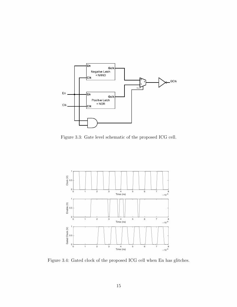
Figure 3.3: Gate level schematic of the proposed ICG cell.
0 1 2 3 4 5 6 7 8Time (ns) ×10-9
0
0.5
1
Clo
ck (V
)
0 1 2 3 4 5 6 7 8Time (ns) ×10-9
0
0.5
1
Enab
le (V
)
0 1 2 3 4 5 6 7 8Time (ns) ×10-9
0
0.5
1
Gat
ed C
lock
(V)
Figure 3.4: Gated clock of the proposed ICG cell when En has glitches.
15

0 0.1 0.2 0.3 0.4 0.5 0.6 0.7 0.8 0.9 1Time (ns) ×10-8
0
0.5
1
Clo
ck (V
)
0 0.1 0.2 0.3 0.4 0.5 0.6 0.7 0.8 0.9 1Time (ns) ×10-8
0
0.5
1
Enab
le (V
)
0 0.1 0.2 0.3 0.4 0.5 0.6 0.7 0.8 0.9 1Time (ns) ×10-8
0
0.5
1
A (V
)
0 0.1 0.2 0.3 0.4 0.5 0.6 0.7 0.8 0.9 1Time (ns) ×10-8
0
0.5
1
B (V
)
0 0.1 0.2 0.3 0.4 0.5 0.6 0.7 0.8 0.9 1Time (ns) ×10-8
0
0.5
1
Sele
ct (V
)
0 0.1 0.2 0.3 0.4 0.5 0.6 0.7 0.8 0.9 1Time (ns) ×10-8
0
0.5
1
GC
lk (V
)
Figure 3.5: Gated clock of the proposed ICG cell including the intermediatesignals.
proper functionality of the proposed ICG cell is illustrated. When En is at
logic high, the output of the MUX follows the clock signal. When clock is 0,
signal A is selected ensuring that no clock edge is missed if there is a glitch
in the En signal during the falling transition of the clock. Alternatively, when
clock is 1, signal B is selected to ensure that all of the clock edges are present
at GClk even when there is a glitch at the En during the rising clock transition.
16

Figure 3.6: Layout of the proposed ICG cell.
In summary, each of the ICG cells for single edge triggered flip-flops ensures
that the glitches propagated to the GClk by the other one are eliminated. The
final result of the circuit is an uninterrupted gated clock signal when the En
is high. The layout of the proposed ICG cell in 45 nm CMOS technology is
depicted in Fig. 3.6.
3.3 Use of the Proposed ICG Cell for Dual
Edge Triggered Flip-flops
The use of dual edge triggered flip-flops has gained popularity in low voltage,
low power circuits for its ability to provide the same throughput while oper-
ating at half the clock frequency [19, 20]. Furthermore, registers having dual
edge triggered flip-flops are more efficient in saving energy than the single edge
triggered flip-flops [21, 22]. Thus, dual edge triggered flip-flops are frequently
used in SoCs for low power applications that require high throughput. There
are various approaches for dual edge triggered flip-flops with inherent clock
gating techniques [23]. One important aim of this thesis is to design an ICG
cell that can be used for any kind of flip-flop. The proposed cell is particularly
effective for dual edge triggered flip-flops as the glitches that may occur in
17

QD
Clk
QD
Clk
0
1Y
SEL0
Positive
Latch[Object]
Negative
Latch[Object]
Clock[Object]
Output[Object]
Data[Object]
Figure 3.7: A traditional dual edge triggered flip-flop using latches and MUX[24].
the En signal at any clock transition are eliminated at the gated clock signal,
thereby ensuring that the dual edge triggered flip-flop does not miss any of
the clock edges to properly latch data.
A traditional dual edge triggered flip-flop is used in this thesis [24]. The
flip-flop incorporates two opposite latches and a MUX, as shown in Fig. 3.7.
The select of the MUX is the clock signal so that the output of the positive
level sensitive latch is selected when clock is 0 and the output of the negative
level sensitive latch is selected when the clock is 1. The output of the MUX
produces the output of the flip-flop.
Figs. 3.8, 3.9 and 3.10 are shown simultaneously to illustrate the difference
between using the proposed ICG cell for clock gating as opposed to using the
existing ICGs. As the latch-AND and latch-NOR ICGs miss clock edges when
En signal has glitches during the clock transitions, the dual edge triggered
flip-flop cannot latch the data for those clock edges, thus providing a wrong
18

0 0.1 0.2 0.3 0.4 0.5 0.6 0.7 0.8 0.9 1Time (ns) ×10-8
00.5
1
Clo
ck (V
)
0 0.1 0.2 0.3 0.4 0.5 0.6 0.7 0.8 0.9 1Time (ns) ×10-8
00.5
1
Enab
le (V
)
0 0.1 0.2 0.3 0.4 0.5 0.6 0.7 0.8 0.9 1Time (ns) ×10-8
00.5
1
Gat
ed C
lock
(V)
0 0.1 0.2 0.3 0.4 0.5 0.6 0.7 0.8 0.9 1Time (ns) ×10-8
00.5
1
Dat
a (V
)
0 0.1 0.2 0.3 0.4 0.5 0.6 0.7 0.8 0.9 1Time (ns) ×10-8
00.5
1
Out
put (
V)
Figure 3.8: Faulty operation of a dual edge triggered flip-flop when gated bya latch-AND based ICG cell.
0 0.1 0.2 0.3 0.4 0.5 0.6 0.7 0.8 0.9 1Time (ns) ×10-8
00.5
1
Clo
ck (V
)
0 0.1 0.2 0.3 0.4 0.5 0.6 0.7 0.8 0.9 1Time (ns) ×10-8
00.5
1
Enab
le (V
)
0 0.1 0.2 0.3 0.4 0.5 0.6 0.7 0.8 0.9 1Time (ns) ×10-8
00.5
1
Gat
ed C
lock
(V)
0 0.1 0.2 0.3 0.4 0.5 0.6 0.7 0.8 0.9 1Time (ns) ×10-8
00.5
1
Dat
a (V
)
0 0.1 0.2 0.3 0.4 0.5 0.6 0.7 0.8 0.9 1Time (ns) ×10-8
00.5
1
Out
put (
V)
Figure 3.9: Faulty operation of a dual edge triggered flip-flop when gated bya latch-NOR based ICG cell.
19
0 0.1 0.2 0.3 0.4 0.5 0.6 0.7 0.8 0.9 1Time (ns) ×10-8
00.5
1
Clo
ck (V
)
0 0.1 0.2 0.3 0.4 0.5 0.6 0.7 0.8 0.9 1Time (ns) ×10-8
00.5
1
Enab
le (V
)
0 0.1 0.2 0.3 0.4 0.5 0.6 0.7 0.8 0.9 1Time (ns) ×10-8
00.5
1
Gat
ed C
lock
(V)
0 0.1 0.2 0.3 0.4 0.5 0.6 0.7 0.8 0.9 1Time (ns) ×10-8
00.5
1
Dat
a (V
)
0 0.1 0.2 0.3 0.4 0.5 0.6 0.7 0.8 0.9 1Time (ns) ×10-8
00.5
1
Out
put (
V)
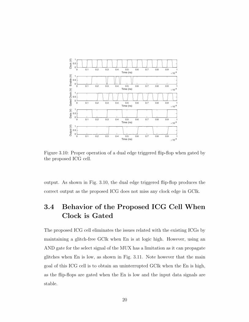
Figure 3.10: Proper operation of a dual edge triggered flip-flop when gated bythe proposed ICG cell.
output. As shown in Fig. 3.10, the dual edge triggered flip-flop produces the
correct output as the proposed ICG does not miss any clock edge in GClk.
3.4 Behavior of the Proposed ICG Cell When
Clock is Gated
The proposed ICG cell eliminates the issues related with the existing ICGs by
maintaining a glitch-free GClk when En is at logic high. However, using an
AND gate for the select signal of the MUX has a limitation as it can propagate
glitches when En is low, as shown in Fig. 3.11. Note however that the main
goal of this ICG cell is to obtain an uninterrupted GClk when the En is high,
as the flip-flops are gated when the En is low and the input data signals are
stable.
20

0 1 2 3 4 5 6 7 8Time (ns) ×10-9
0
0.5
1
Clo
ck (V
)
0 1 2 3 4 5 6 7 8Time (ns) ×10-9
0
0.5
1
Enab
le (V
)
0 1 2 3 4 5 6 7 8Time (ns) ×10-9
0
0.5
1
Gat
ed C
lock
(V)
Figure 3.11: GClk if there are glitches when En is zero.
3.5 Sensitivity of the Proposed ICG Cell to
Glitch Pulse-Width
Another important issue in the proposed ICG cell is the shortened pulse-width,
as shown in Fig. 3.12 where a glitch occurs during the rising transition of the
clock. As the En becomes zero for a short time interval, the MUX selects
signal A rather than signal B. Thus, the pulse width of the gated clock signal
is shortened in proportional to the pulse width of the glitch. In practice, the
glitches are fast with sufficiently small pulse widths, and this effect can be
ignored, provided that the gated clock signal does not miss any transitions.
As discussed above, the proposed ICG cell provides a glitch-free and un-
interrupted gated clock signal for all of the three kinds of flip-flops when the
En signal is high. The proposed cell is compared with the existing ICG cells
21

0 1 2 3 4 5 6 7 8Time (ns) ×10-9
0
0.5
1
Clo
ck (V
)
0 1 2 3 4 5 6 7 8Time (ns) ×10-9
0
0.5
1
Enab
le (V
)
0 1 2 3 4 5 6 7 8Time (ns) ×10-9
0
0.5
1
Gat
ed C
lock
(V)
Figure 3.12: A smaller pulse-width in gated clock signal when there is a glitchin En during the rising transition of the clock.
in terms of power consumption, delay and layout area, as discussed in the
following section.
22

3.6 Performance Comparison
The performance of the proposed ICG cell is compared with the existing ICG
cells. All of the ICG cells are simulated using 45 nm CMOS technology and
are operated by a supply voltage of 1.0 V at a clock frequency of 1 GHz.
Avg. Power Avg. PowerConsump- Consump- Clk to Glitch
ICG tion when tion when GClk Layout Character-cell Clock is Clock is Delay Area istics
Not Gated Gated(µW ) (µW ) (ps) (µm2)
Latch- glitchesAND 9.13 2.22 51.11 3.816 occur1
basedLatch- glitchesNOR 7.47 1.72 42.36 3.816 occur2
basedProposed no
ICG 22.31 4.09 86.14 10.137 glitches3
cell
Table 3.1: Performance comparison of the proposed ICG cell with the existingICG cells.
A comparative analysis between the proposed ICG cell and the existing
ICG cells are listed in Table 3.1. According to Table 3.1, the proposed ICG
cell has higher latency and increased power consumption (by almost a factor
of 2 to 2.5 when compared to the existing ICGs). However, note that a reliable
1When there is a glitch in the En during rising clock transition.2When there is a glitch in the En during falling clock transition.3When there is a glitch in the En during both rising and falling clock transitions.
23
and glitch-free gated clock signal is obtained despite the glitches in the enable
signal. Furthermore, the proposed ICG cell is particularly applicable to dual
edge triggered flip-flops since the enable signal may exhibit glitches during
both transitions.
24

Chapter 4
Conclusion
Integrated clock gating cell is an important component of low power circuits
since clock gating is a typical practice to reduce dynamic power consumption.
New techniques such as intelligent clock gating and energy recovery clock gat-
ing have been proposed to satisfy the demand of low power and high speed
circuits [25,26].
In this thesis, a new ICG cell is proposed with guaranteed glitch-free gated
clock signal for both single edge and dual edge triggered flip-flops. The pro-
posed cell is compared with the existing ICG cells. The existing ICG cells
produce a faulty gated clock signal if glitches occur in the enable signal during
the transitions of the clock. The proposed ICG cell eliminates this issue and
ensures an uninterrupted gated clock. As dual edge triggered flip-flops are
preferable for high throughput circuits, the proposed ICG cell can be highly
useful for these applications.
All of the three ICG cells were designed and simulated in 45 nm CMOS
technology. The comparison results demonstrate that higher reliability is
achieved at the expense of higher delay and greater power consumption.
25

Appendix A
Schematic Figures
Figure A.1: Schematic diagram of the proposed ICG cell.
26

Figure A.2: Schematic diagram of the latch-AND ICG cell.
Figure A.3: Schematic diagram of the latch-NOR ICG cell.
27

Figure A.4: Schematic diagram of the dual edge triggered flip-flop.
28
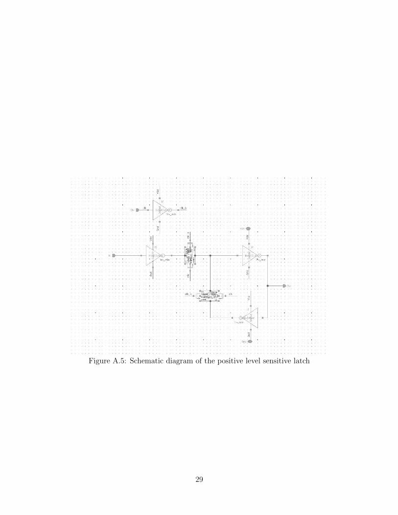
Figure A.5: Schematic diagram of the positive level sensitive latch
29

Figure A.6: Schematic diagram of the negative level sensitive latch
30

Figure A.7: Schematic diagram of the 2 to 1 multiplexer
31

Bibliography
[1] L. Benini, G. D. Micheli, E. Macii, M. Poncino, and R. Scarsi, “Symbolic
synthesis of clock-gating logic for power optimization of control-oriented
synchronous networks,” in European Design and Test Conference, Mar
1997, pp. 514–520.
[2] M. Saint-Laurent and A. Datta, “A low-power clock gating cell optimized
for low-voltage operation in a 45-nm technology,” in Proceedings of the
ACM/IEEE International Symposium on Low-Power Electronics and De-
sign (ISLPED), Aug 2010, pp. 159–163.
[3] M. Horowitz, T. Indermaur, and R. Gonzalez, “Low-power digital design,”
in Low Power Electronics, Digest of Technical Papers., IEEE Symposium,
Oct 1994, pp. 8–11.
[4] W. Liu, E. Salman, B. Taskin, and C. Sitik, “Clock skew scheduling
in the presence of heavily gated clock networks,” in Proceedings of the
ACM/IEEE Great Lakes Symposium on VLSI, May 2015, pp. 283–288.
[5] W. Liu, E. Salman, C. Sitik, and B. Taskin, “Exploiting useful skew in
gated low voltage clock trees for high performance,” in Proceedings of the
IEEE Int. Symposium on Circuits and Systems, May 2016.
32

[6] C. Sitik, W. Liu, B. Taskin, and E. Salman, “Design methodology for
voltage-scaled clock distribution networks,” IEEE Transactions on Very
Large Scale Integration (VLSI) Systems, vol. PP, no. 99, pp. 1–14, 2016.
[7] C. Sitik, L. Filipini, E. Salman, and B. Taskin, “High performance low
swing clock tree synthesis with custom d flip-flop design,” in Proceedings
of the IEEE Computer Society Annual Symposium on VLSI, July 2014,
pp. 498–503.
[8] C. Sitik, E. Salman, L. Filippini, S. J. Yoon, and B. Taskin, “Finfet-
based low-swing clocking,” ACM Journal on Emerging Technologies in
Computing Systems (JETC), vol. 12, no. 13, August 2015.
[9] M. Rathore, W. Liu, E. Salman, C. Sitik, and B. Taskin, “A novel
static d flip-flop topology for low swing clocking,” in Proceedings of the
ACM/IEEE Great Lakes Symposium on VLSI, May 2015, pp. 301–306.
[10] E. Salman and E. G. Friedman, High Performance Integrated Circuit De-
sign. Mcgraw-Hill, 2012.
[11] S. Huda, M. Mallick, and J. H. Anderson, “Clock gating architectures
for fpga power reduction,” in International Conference on Field Pro-
grammable Logic and Applications, Aug 2009, pp. 112–118.
[12] V. Tiwari, D. Singh, S. Rajgopal, G. Mehta, R. Patel, and F. Baez,
“Reducing power in high-performance microporecessors,” in Proceedings
of the 35th annual Design Automation conference, 1998, pp. 732–737.
33

[13] J. Kathuria, M. Ayoubkhan, and A. Noor, “A review of clock gating tech-
niques,” MIT International Journal of Electronics and Communication
Engineering, vol. 1, no. 2, pp. 106–114, 2011.
[14] B. Pangrie and P.-H. Ho, “Placement driven power optimization at 90nm
and below,” SOCcentral, 2005.
[15] Y. S. Park, Y. Tao, and Z. Zhang, “A 1.15gb/s fully parallel nonbinary
ldpc decoder with fine-grained dynamic clock gating,” in IEEE Inter-
national Solid-State Circuits Conference Digest of Technical Papers, Feb
2013, pp. 422–423.
[16] A. Shrivastava, “Clock gating: Smart use ensures smart returns,”
www.embedded.com, 2009.
[17] A. G. M. Strollo, E. Napoli, and D. D. Caro, “New clock-gating techniques
for low-power flip-flops,” in Proceedings of the International Symposium
on Low Power Electronics and Design, 2000, pp. 114–119.
[18] R. Bhutada and Y. Manoli, “Complex clock gating with integrated clock
gating logic cell,” in Proceedings of the International Conference on De-
sign Technology of Integrated Systems in Nanoscale Era, Sept 2007, pp.
164–169.
[19] W. Chung, T. Lo, and M. Sachdev, “A comparative analysis of low-power
low-voltage dual-edge-triggered flip-flops,” IEEE Transactions on Very
Large Scale Integration (VLSI) Systems, vol. 10, no. 6, pp. 913–918, Dec
2002.
34

[20] C. Kim and S.-M. Kang, “A low-swing clock double-edge triggered flip-
flop,” IEEE Journal of Solid-State Circuits, vol. 37, no. 5, pp. 648–652,
May 2002.
[21] R. Hossain, L. D. Wronski, and A. Albicki, “Low power design using
double edge triggered flip-flops,” IEEE Transactions on Very Large Scale
Integration (VLSI) Systems, vol. 2, no. 2, pp. 261–265, June 1994.
[22] N. Nedovic, M. Aleksic, and V. G. Oklobdzija, “Timing characterization
of dual-edge triggered flip-flops,” in Proceedings of the International Con-
ference on Computer Design, 2001, pp. 538–541.
[23] X. Wang and W. H. Robinson, “A low-power double edge-triggered flip-
flop with transmission gates and clock gating,” in Proceedings of IEEE
International Midwest Symposium on Circuits and Systems, Aug 2010,
pp. 205–208.
[24] T. A. Johnson and I. S. Kourtev, “A single latch, high speed double-edge
triggered flip-flop (detff),” in The 8th IEEE International Conference on
Electronics, Circuits and Systems, vol. 1, 2001, pp. 189–192.
[25] F. Rivoallon and J. Balasubramanian, “Reducing switching power with
intelligent clock gating,” Xilinx WP370 (v1.1), 2010.
[26] V. Tirumalashetty and H. Mahmoodi, “Clock gating and negative edge
triggering for energy recovery clock,” in IEEE International Symposium
on Circuits and Systems, May 2007, pp. 1141–1144.
35