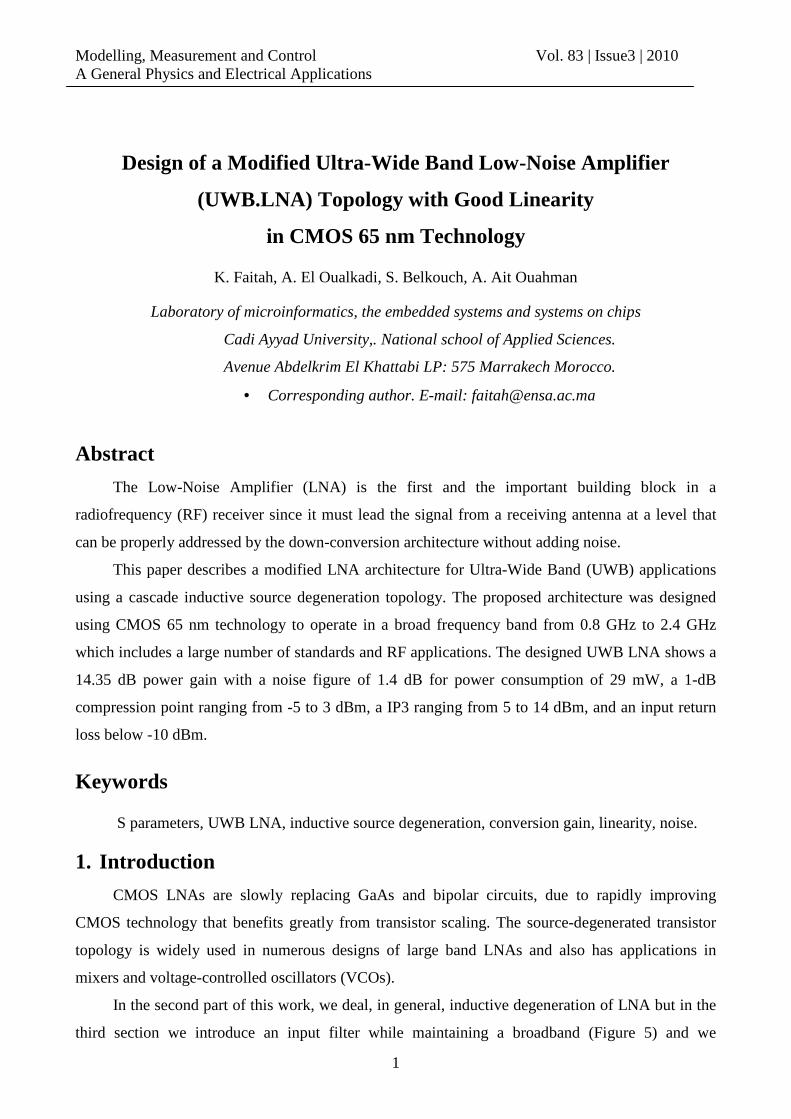
Design of a Modified Ultra-Wide Band Low-Noise Amplifier ...
24
HAL Id: hal-00947382 https://hal.inria.fr/hal-00947382 Submitted on 15 Feb 2014 HAL is a multi-disciplinary open access archive for the deposit and dissemination of sci- entific research documents, whether they are pub- lished or not. The documents may come from teaching and research institutions in France or abroad, or from public or private research centers. L’archive ouverte pluridisciplinaire HAL, est destinée au dépôt et à la diffusion de documents scientifiques de niveau recherche, publiés ou non, émanant des établissements d’enseignement et de recherche français ou étrangers, des laboratoires publics ou privés. Design of a Modified Ultra-Wide Band Low-Noise Amplifier (UWB.LNA) Topology with Good Linearity in CMOS 65 nm Technology Khalid Faitah, Ahmed El Oualkadi, Said Belkouch, Abdellah Ait Ouhaman To cite this version: Khalid Faitah, Ahmed El Oualkadi, Said Belkouch, Abdellah Ait Ouhaman. Design of a Modified Ultra-Wide Band Low-Noise Amplifier (UWB.LNA) Topology with Good Linearity in CMOS 65 nm Technology. Modelling, Measurement and Control, A General Physics and Electrical Applications, AMSE, 2010, 83 (3). hal-00947382
Transcript of Design of a Modified Ultra-Wide Band Low-Noise Amplifier ...

HAL Id: hal-00947382https://hal.inria.fr/hal-00947382
Submitted on 15 Feb 2014
HAL is a multi-disciplinary open accessarchive for the deposit and dissemination of sci-entific research documents, whether they are pub-lished or not. The documents may come fromteaching and research institutions in France orabroad, or from public or private research centers.
L’archive ouverte pluridisciplinaire HAL, estdestinée au dépôt et à la diffusion de documentsscientifiques de niveau recherche, publiés ou non,émanant des établissements d’enseignement et derecherche français ou étrangers, des laboratoirespublics ou privés.
Design of a Modified Ultra-Wide Band Low-NoiseAmplifier (UWB.LNA) Topology with Good Linearity in
CMOS 65 nm TechnologyKhalid Faitah, Ahmed El Oualkadi, Said Belkouch, Abdellah Ait Ouhaman
To cite this version:Khalid Faitah, Ahmed El Oualkadi, Said Belkouch, Abdellah Ait Ouhaman. Design of a ModifiedUltra-Wide Band Low-Noise Amplifier (UWB.LNA) Topology with Good Linearity in CMOS 65 nmTechnology. Modelling, Measurement and Control, A General Physics and Electrical Applications,AMSE, 2010, 83 (3). hal-00947382
Modelling, Measurement and Control Vol. 83 | Issue3 | 2010 A General Physics and Electrical Applications
1
Design of a Modified Ultra-Wide Band Low-Noise Amplifier
(UWB.LNA) Topology with Good Linearity
in CMOS 65 nm Technology
K. Faitah, A. El Oualkadi, S. Belkouch, A. Ait Ouahman
Laboratory of microinformatics, the embedded systems and systems on chips
Cadi Ayyad University,. National school of Applied Sciences.
Avenue Abdelkrim El Khattabi LP: 575 Marrakech Morocco.
• Corresponding author. E-mail: [email protected]
Abstract
The Low-Noise Amplifier (LNA) is the first and the important building block in a
radiofrequency (RF) receiver since it must lead the signal from a receiving antenna at a level that
can be properly addressed by the down-conversion architecture without adding noise.
This paper describes a modified LNA architecture for Ultra-Wide Band (UWB) applications
using a cascade inductive source degeneration topology. The proposed architecture was designed
using CMOS 65 nm technology to operate in a broad frequency band from 0.8 GHz to 2.4 GHz
which includes a large number of standards and RF applications. The designed UWB LNA shows a
14.35 dB power gain with a noise figure of 1.4 dB for power consumption of 29 mW, a 1-dB
compression point ranging from -5 to 3 dBm, a IP3 ranging from 5 to 14 dBm, and an input return
loss below -10 dBm.
Keywords
S parameters, UWB LNA, inductive source degeneration, conversion gain, linearity, noise.
1. Introduction
CMOS LNAs are slowly replacing GaAs and bipolar circuits, due to rapidly improving
CMOS technology that benefits greatly from transistor scaling. The source-degenerated transistor
topology is widely used in numerous designs of large band LNAs and also has applications in
mixers and voltage-controlled oscillators (VCOs).
In the second part of this work, we deal, in general, inductive degeneration of LNA but in the
third section we introduce an input filter while maintaining a broadband (Figure 5) and we

Modelling, Measurement and Control Vol. 83 | Issue3 | 2010 A General Physics and Electrical Applications
2
eventually interpreted source noises and how to optimize over several papers including the most
recent like [8] which decreased the noise taking into account a certain capacity nodal Cx
representing all parasitic capacitances between the two transistors cascade. As against in our work,
we chose an output resonant filter with inductors mostly very low values to reduce further the noise.
The fourth part, by the Figure 10, we proposed our LNA architecture using two filters and the
transistors with sizes appropriate to have a high transconductance and possibly gain still at
reasonable level while ensuring a minimum of noise along our frequency range 0.8 GHz to 2.42
GHz.
2. Review of the LNA architectures using inductive source degeneration topology
The LNAs are classified into four categories. They are defined by the type of the input
impedance showed at the input building block. Indeed, the compromise between the noise figure
and the gain is essentially resolved by matching the LNA input. Figure 1 shows various LNA
topologies commonly encountered in the bibliography [1] [2].
0 0
.
M
RZin.
(a) Resistor ending
M
0
Zin
0
R
R
.
.
(b) Amplifier with resistors
Zin
0
.M
.
(c) Amplifier with mg
1
ending
Lg
.
.
Zin
Ls
0
M
(d) Inductively degenerated common-
source
Figure 1: Different topologies of LNAs.
In this paper, a LNA architecture using inductive source degeneration topology is proposed
and designed. As has been illustrated in several publications [3.4.7.8.9.], this architecture using
inductive source degeneration gives a perfect matching without adding noise to the system and
without imposing any restrictions on the gm conductance. This perfect matching can be obtained by
using two inductors: the source inductor LS and the gate inductor Lg, as shown in Figure 2.

Modelling, Measurement and Control Vol. 83 | Issue3 | 2010 A General Physics and Electrical Applications
3
.
Vs
Iout
.Ve
Ls
M1
Rs Lg
0
Zin
Figure 2: LNA architecture using inductive source degeneration topology
From Figure 2, the input impedance of the LNA is defined by Zin = ei
Ve (1)
By replacing the transistor M1 by its equivalent small signal circuit and taking into account
the no quasi-static resistor of the gate transistor, the obtained equivalent circuit is shown in Figure 3:
. v
Ve
Rg gsnqs
Zin
0
Lg..
g
ie
m
Ls
0
Cgs
Figure 3: Equivalent circuit of LNA taking into account the nqsgR resistor
In our frequency range a small signal analysis remains appropriate while neglecting the Cgd capacitor of the transistor M1, this gives:
( )gsmesegegs
ege VgijLiRijC
1ijLV
nqs+ω++
ω+ω= (2)
as : egs
gs ijC
1V
ω= , then : ( )
nqsgsTgs
sgin RLCj
1LLjZ +ω+
ω++ω= (3)
where gs
mT C
g=ω .
At the resonant frequency, the capacitive effect cancels the inductive effect; the input
impedance can be given by:
( )nqsgsTeqRin RLRZ +ω==ω (4)

Modelling, Measurement and Control Vol. 83 | Issue3 | 2010 A General Physics and Electrical Applications
4
where: ( ) gssgR
CLL += 1ω is the resonance frequency. In fact, the L.C resonator improves the
gain of the LNA. Then, as can be shown at the input of the circuit (figure 3), the quality factor is
given by: eqRgs RC
1Q
ω= (5)
At the resonance frequency, the voltage magnitude across gsC is Q multiplied by the voltage
across the input, which has the effect of increasing the effective transconductance Gm of the circuit:
Gm = Q.gm (6)
Typically this Q factor reduces the noise returned by the input while increasing the gain. But
the biggest handicap of this topology remains its application narrowband and bad isolation.
In Figure 4, a cascode stage is added to reduce both the interaction between the input and
output and the reverse gain (form output to the input). This reduction has the effect of increasing the
stability of the amplifier [2].
.
Lg
0
Vout
Vdd
.
L
Vcas
Rs.
M2
L
Ls
Vs M1
Ve
.
Zin
Figure 4: LNA using a cascode inductive source degeneration topology
Moreover, the cascode topology reduces the effect of the capacitor gdC of M1 by presenting a
low-impedance at the drain of M1. The output inductor LL is chosen to resonate at the frequency of
the input signal with the output capacitor.
By using this topology, we could have a wider and a smoother frequency response by aligning
the resonance at the input with that of the output, which also has the effect of achieving a high gain.

Modelling, Measurement and Control Vol. 83 | Issue3 | 2010 A General Physics and Electrical Applications
5
3. Theoretical study of the proposed UWB LNA
In the literature, a large number of the LNA architectures are narrowband and are optimized
to work for a single frequency [17], [18], [19], [20], [21]. In the proposed architecture, as shown in
Figure 5, an extension of the inductive source degeneration topology is adopted to achieve a broad
frequency band matching impedance.
0
Ve
0
3L
Cp
C
Lg
Vs
1
.
2
Zin
C
.
L
0
M1
2
Ls
1
Iout
3NN
Rs
L
L
0
C
C
Figure 5: UWB LNA with an inductive source degeneration topology
The equation (3) can be written:
Tt
tt
sm
ttin R
CjLj
C
Lg
CjLjZ ++=++=
ωω
ωω 11
(7)
where Ct = Cp + Cgs , Lt = Lg + Ls and t
smT C
LgR = , the capacitor Cp has been added to increase
the degree of freedom of the system, this could increases the total capacity between the gate and the
source of M1.
By combining Li , Ci et Zin (Figure 5), the architecture will be equivalent, as shown in
Figure 6, to a passband filter with a output load RT.
To ensure the design of an UWB LNA and to facilitate the implementation of inductors, a
compromise must be made between the choice of the number of LC elements and the values of
inductors [3], [4].

Modelling, Measurement and Control Vol. 83 | Issue3 | 2010 A General Physics and Electrical Applications
6
0
2
0
Z's
0
t
1
0
L
Z'in
C3
Zin
L
R
N
T
NC 3 C1L
Lg + Ls2L C C
Figure 6: Input building block of the LNA
3.1 Gain calculation
The gain of the cascode LNA in Figure 4 is equal to the multiplication product of the
amplification due to the transistor M1 and that produced by the transistor M2.
The transistor M2 is mounted on a common base, known by the amplification of mg
1. Then,
this topology makes a good impedance matching to 50 Ω, its gain is given by:
22M2
.AV MM loadm Zg= (8)
The transfer function of the filter in Figure 6 is:
in
Rpb V
VjTF T=)( ω (9)
Therefore the input current i in is:
T
inpbin R
VjTFi ).( ω= (10)
The voltage Vgs of M1 can be found directly by multiplying the current iin by the impedance
across the source-gate of M1:
tT
pbin
t
ings CRj
jTFV
Cj
iV
ωω
ω)(
== (11)
Using the equation (6), the effective transconductance of M1 is given by:
tT
pbm
in
gsmm CRj
jTFg
V
VgjG M
MM ωω
ω)(.
)( 1
11== (12)
At the resonance frequency, the Q factor of the circuit in figure 6 is similar to that found in
equation (5):
tRt RC
Qω1= (13)

Modelling, Measurement and Control Vol. 83 | Issue3 | 2010 A General Physics and Electrical Applications
7
then )(..11
ωjTFQgG pbmm MM= (14)
The advantage of this circuit is its effective transconductance which is depended to the quality
factor Q, which will allow to increase its value.
The voltage amplification of M1 is:
111
.MMM loadmV ZGA −= (15)
However, M2 is mounted on a common base, therefore, 2
1
1
MM
mload
gZ = represents its input
impedance. So the voltage amplification of the LNA cascode is:
22
2
1
21...
MMM
M
MM loadmm
mVVV Zg
g
GAAA −== , then :
21
.MM loadmV ZGA −= (16)
3.2 Noise analysis
In this topology, two types of noise may persist, one comes from the quality factor of the
input network, and the other comes from both the gate source noise and the drain source noise of
M1. To study the effect of noise coming from the transistor, we will follow an analysis similar to
that made in reference [3].
The input transistor with source degeneration including its gate and drain noises are shown in
Figure 7.a. These two sources of noise, as shown in Figure 7.b, may be replaced by a voltage source
and a current source at the input:
Ls
00
*
n
*
(a)
i²M1
n
nd
(b)
v²
ng
M1Cpi²
Ls
*i²
0
* Cp
Figure 7: Models of noise in transistor M1 with source degeneration

Modelling, Measurement and Control Vol. 83 | Issue3 | 2010 A General Physics and Electrical Applications
8
These sources have expressions like:
ndm
tngn i
g
Cjii
ω+= and ( ) nsm
nd
m
ndtsndsn iLj
g
i
g
iCLiLjv ωωω +=−+= 21
Their spectral densities can be given by:
fgTKi dBnd ∆= 02 4 γ and f
g
CTKi
d
gsBng ∆=
0
222
54
ωδ correlated with a coefficient:
jii
iic
ndng
ndng 395.0.
.
22
*
−≈= with 0dg is the drain-source conductance at Vds = 0V.
The value of the technological parameter γ is typically 2 to 3, because of heating due to the
intense electric field in short channels of CMOS transistors.
δ = 2.γ is the noisy coefficient of the gate.
Indeed, there is a correlation between the noise generator current and voltage thus:
in = ic + iu , where ic is the correlated part with vn and iu is the correlated part with in, then:
ic=Yc.vn , Yc is the admittance of correlation.
However, the noise figure is given [5]:
2
22
s
nsns
i
vYiiF
++=
(17)
With is and Ys are respectively the current and the admittance of source. Thus:
2
222
2
22
1)(
s
ncsu
s
ncsus
i
vYYi
i
vYYiiF
+++=
+++= (18)
This last expression shows that the noise is caused by three independent sources whose
resistance and the admittances defined by:
fTK
vR
B
nn ∆
=4
2 ,
fTK
iG
B
uu ∆
=4
2 and
fTK
iG
B
ss ∆
=4
2. (19)
(18) and (19) imply : ( ) ( )[ ]
s
nscscu
s
ncsu
G
RBBGGG
G
RYYGF
222
11+++++=
+++= (20)
where Yc = Gc + j Bc and Ys= Gs+ jBs . To design an optimal source which allows to generate the
minimum of noise, it is important to derive the equation (20) according to its conductance Gs and its
susceptance "reactance" Bs and to put the derivative to zero, the optimal values are the following:

Modelling, Measurement and Control Vol. 83 | Issue3 | 2010 A General Physics and Electrical Applications
9
=+=
=−=
optn
ucs
optcs
GR
GGG
BBB
2 (21)
This gives a minimum of noise : ( )coptn GGRF ++= 21min .
If we replace this in the general equation (20) of the noise, we get:
( ) ( )[ ]22min optsopts
s
n BBGGG
RFF −+−+= (22)
The expression (22) is a circle of center (Gopt , Bopt) and radius ( )minFFR
G
n
s − , when F tends
towards its minimum, this circle coincides with the center, but when the noise source generates a
variable factor F, it will have a contour which is no longer a circle but a conical.
In the case of our circuit and considering: t
gs
C
C=ρ ,
γδχ5
= and 0d
m
g
g=α (considerable
factor for the short channels), the admittance of correlation between in and vn and is: [3]
222221
1.
ωχαρραχ
ραχω
ts
tcc
n
cc
CLc
c
jCBjG
v
iY
−++
+=+== (23)
n
u
n
ucopt R
G
R
GGG =+= 2 , in references [6] and [7] a similar calculation gives:
( )2
222
1
21
c
cCG t
opt−
++=
ραχ
χαρραχω (24)
2222
21
1
χαρραχραχ
ω
ω
++
+−
=−=
c
cCL
CBB
ts
tcopt (25)
as ( )
−
++=
2222
2220
2
1.
21.
c
cgG d
uχαργ
χαρραχα and ( )22222
2
21.. χαρραχωγα
++=
cC
gR
t
dàn
Like in reference [4] the optimal source which will generate less noise must verifies the
following relation 12 =ωtsCL
Then: ( ) ( )αγωω .1
11
1 smn
s
su Rg
P
R
R
RGF
M
+=++= (26)

Modelling, Measurement and Control Vol. 83 | Issue3 | 2010 A General Physics and Electrical Applications
10
Where ( ) ( )222222222
2222
2121
1χαρραχω
χαρραχ
χαρω +++
++
−
= cCRc
cP ts (27)
In fact, such analysis was made only for M1 but the cascode stage generates also a noise
source which is due to the "presence" of a parasite Nodal capacitor Cx at the drain of M2 [8]. In our
proposed design which uses a CMOS 65 nm technology, the noise due to Cx can be neglected
compared to the noise of the amplifier stage based on M1.
4. Design of the proposed UWB LNA (0.8-2.4 GHz)
The proposed UWB LNA design, using a cascade inductive source degeneration topology, is
shown in Figure 8. This modified architecture contains a second order passband filter at the input.
This passband filter allows achieving the desired frequency band with inductors whose values
below 7 nH which permits to reach a stable gain. The modified architecture includes also a bias
circuit which can be demonstrated thereafter.
L
Ls
Vcas
L
C
Vin
C
.
0
Vdd
0
L
Lg
L
.
1L
Cp
Z'in
M1
.
R
M2
Vout
1
.
Figure 8: UWB LNA with a second order passband filter

Modelling, Measurement and Control Vol. 83 | Issue3 | 2010 A General Physics and Electrical Applications
11
The transistor M1 is designed so as to have a high 1Mmg to ensure a satisfactory amplification
with a minimal noise, while the transistor M2 represents a point of a low impedance to minimize the
effect of the capacitor Cgd and to increase the isolation of the circuit.
The output of the circuit is a parallel RLC should resonate, as we will see in paragraph
( ∫ c.2.4 ), at a high frequency than the maximum of the useful frequency band. The choice of this
circuit as output network to replace the "shunt peaking" method [7] comes from the reasonable
value of inductance in the band 0.8-2.4GHz.
4.1. Design of the input building block (passband filter)
Figure 9 shows the passband filter which uses four poles.
t
R
Zin
C
0
L
Z'in
Lg + Ls
T
C
0
11
Figure 9: Equivalent circuit of the input passband filter
The calculation of the transfer function of such a filter gives:
1....
.
12111
3111
411
21
+
++
+++
++=
pR
LCRp
R
CLRCLCLp
R
CLLCLCRpCLCL
pCLR
R
V
V
tTtT
tttt
tTtt
tT
e
RT (28)
Ve is the voltage across the source which has an intern resistor R = 50 Ω and p = jω is the
Laplace operator.
The equation (28) can be expressed by:
1..2.2
..2
.1
.
)(
20
22
20
20
340
440
22
20
+∆+
∆++∆+
∆
=
pppp
p
pFTpb
ωω
ωω
ωωω
ω
ωω
(29)
ω0 is the central frequency of the filter and ∆ω is the passband of the filter (difference between the
high and low cutoff frequencies).

Modelling, Measurement and Control Vol. 83 | Issue3 | 2010 A General Physics and Electrical Applications
12
By identification, we can obtain the system of equations (30) which will allow calculating the
elements of the filter.
∆=
∆=+
∆+=++
∆=+
=
2
20
1
20
1
2
20
20
111
40
111
40
11
.2
2
.2
1
ωω
ωω
ωω
ω
ωω
ω
R
CLR
R
LCR
R
CLRCLCL
R
CLLCLCR
CLCL
tT
tT
tTtt
tttT
tt
(30)
(30.c) – (30.e) ⇒ 20
112
ω=+ ttCLCL , considering
40
111
ω=ttCLCL then:
20
111
ω== ttCLCL (31)
By substituting (31) in (30.b), we get:
20
1 .2ω
ω∆=+R
LCR tT (32)
(32) and (30.e) imply:
20
1
ωω∆==
R
LCR tT (33)
We have three equations (31), (32) and (33) linearly independent and five unknown, a choice
must be made to set two unknowns and therefore find the values of others. Indeed, the values of RT
and R (the source resistor) have been set to 50 Ω, this could achieve a good impedance matching.
What gives:
==
nHL
nHL
t 97.4
49.61 and
==
pFC
pFCt
99.1
6.2
1 considering sgt LLL += and gspt CCC +=
RT is equal to t
sm
C
LgM
.1 then :
(30.a)
(30.b)
(30.c)
(30.d)
(30.e)

Modelling, Measurement and Control Vol. 83 | Issue3 | 2010 A General Physics and Electrical Applications
13
1Mm
tTs
g
CRL = (34)
To set the values of Ls and Cp, we have configured the size of the transistor M1 in order to
deduce the values of 1Mmgand Cgs .
4.2. Sizes of M1 and M2
a. Transistor M1
Considering the useful frequency band (0.8 GHz - 2.4 GHz) and the technology adopted
(CMOS 65nm), we can write:
( )Tgsm
D VVg
i M −=1
1
21 (35)
Where iD1 is the current drain of M1 and VT is its threshold voltage conduction.
( )TgsOXnm VVL
WCg
M−=
11.µ (36)
Where COX is the surface capacitor of the gate-channel of M1, µn is the mobility of carriers; L and
W are respectively the gate length and the channel width of the M1 transistor.
From the reference [10] and by considering the CMOS 65 nm technology with a voltage
supply VDD equals to 1.8 V, we can have: sVmn ./0218.0 2=µ and 215 /106.18 mFCOX µ−×= .
The current iD1 is fixed equal to 16 mA to minimize the power consumption lower than a
threshold of 30 mW.
To minimize the variation effect of VT according to the temperature, a series of simulation
have been realized. The result is that, for a difference of potential Vgs1 – VT approximately equal to
0.16 V the quotient L
W is sufficiently higher. This gives, from relation (35), a suitable
transconductance 1Mmg which is roughly equal to 200 mA/V.
By replacing the value of 1Mmg in (36) we obtain. 77.3082=
L
W.
By considering L = 0.1 µm this gives 2.308≈W µm.
LWCC OXgs ...3
21 = then Cgs1 = 0.382 pF.
Cp = Ct – Cgs1 = 2.22 pF. From equation (34) Ls = 650 pF, then Lg = Lt – Ls = 4.32 nH.
b. Transistor M2
The size of the transistor M2 has been chosen equal to that of M1 to improve its isolation and
ensure the stability of the circuit while minimizing the effect of capacitor Cgd.

Modelling, Measurement and Control Vol. 83 | Issue3 | 2010 A General Physics and Electrical Applications
14
c. Design of the output building block
In the relation (16) 2MloadZ is a RLC parallel circuit, as illustrated on Figure 8, its
components must be sized according to the total gain of the circuit.
1..
.
22
++=
pR
LpCL
PLZ
L
LLL
LloadM
(37)
)37(
)16(
)12(
⇒ ( )pTFpCRp
R
LpCL
PLgA pb
tT
L
LLL
LmV M
.1
.1..
..
21
++−= (38)
Knowing that t
smT C
LgR M1= then the total gain AV writes as:
( )pTFp
R
LpCLL
LA pb
L
LLL
s
LV .
1..
1.
2 ++−= (39)
Ls is set equal to 4.32 nH, to increase the gain AV we can adjust the value of LL but an
excessive value may deteriorate the frequency response of the gain. This may occur if the cutoff
frequency of the lowpass filter, produced by the RLC parallel circuit, becomes lower than the high
cutoff frequency of the passband filter.
A compromise must be made, a cutoff pulsation ωc of the RLC network roughly equal to
3 GHz has been choosing. Then:
=
=
cL
L
cLL
R
L
CL
ωζω
.2
12
(40)
where ζ is the damping coefficient which must be less than 2 to ensure a resonance at the
cutoff frequency. We have considering that 2.ζ = 1 and RL = 50 Ω to ensure a perfect impedance
matching. Then:
LL = 2.65 nH and CL = 1.06 pF.
4.3. Full schematic of the proposed UWB LNA
In figure 10, the bias circuit is a current mirror cascode, with transistors Mb1 and Mb2 identical
to those of the LNA.

Modelling, Measurement and Control Vol. 83 | Issue3 | 2010 A General Physics and Electrical Applications
15
0
2
M1.
big1
L
VcasMb
1L
M2
in
Iin
C
RL
big2
.
b1
RF
0
L
C
1
Vdd
RF
Ls0
C
0
L
out
R
C
2 Lg
.
Mb
2
C
1
L
.
Cp
Figure 10: Full schematic of the circuit (LNA and the bias circuit)
The values of the components founded, by theoretical calculation, don’t really reach the
performance needed. Indeed, the power gain is below 10 dB and the matching at the input is above
than -10 dB.
After several simulations, optimal results are found and illustrated in Table 1.
L1(nH) C1(pF) Lg(nH) LS(pH) Cp(pF) Cgs(pF) LL(nH) CL(pF) RL(Ω)
Theoretical value
6.49 1.99 4.32 650 2.22 0.382 2.65 1.06 50
Adjusted value
4.97 2 4.277 700 1.673 0.382 4 1 350
Table 1 : Theoretical and adjusted values of input and output of the LNA network
For the isolation of RF signal and the circuit, a LC circuit has been added at the input of the
passband filter which has the same values as Lt and Ct in order to not affect the transfer function of
the input filter.
The table 2 shows a performance comparison with the results obtained in recent publications.

Modelling, Measurement and Control Vol. 83 | Issue3 | 2010 A General Physics and Electrical Applications
16
Paper Tech S11[dB] Gmax [dB]
B[GHz] N.F[dB] IIP3
[dBm] ICP
[dBm] Pdiss
[mW]
[11] 0.18µm CMOS
<-10 17.8 2.4∼ 3.3 3.5∼ 5 -13 -17 39.6
[12] TCMC0.1
8µm <-10 17.5 0.86∼ 0.96 4.1 5.4∼ 14.3 -4.5 15.5
[13] 0.18µm CMOS
<-8.7 13.1 3.1∼ 12.2 2.7∼ 4.9 -- -- 13.9
[14] 90 nm CMOS
-10 14.6 <5.5 -- -- 24
[15] 0.13µm CMOS
-15 12 8.8 -- -- 54
[16] 65nm -16.84 10.02 8.68 -- -- 18.5 This Work
65 nm CMOS
<-10 14.35 0.8∼ 2.4 1.4 5 à 14 -5 à 3 29
Table 2: Comparison of the UWB LNA performance with recent publications
5. Design results and discussions
5.1 Gain of the UWB LNA
The figure 11 shows the gain versus the input frequency for various input powers ranging
from -40 dBm to -5 dBm. It is shown that the gain has a form similar to a passband filter amplified
by approximately 14.35 dB.
Figure 11: Gain versus frequency for different values of the power input
Frequency (GHz)
Gain (dB)

Modelling, Measurement and Control Vol. 83 | Issue3 | 2010 A General Physics and Electrical Applications
17
5.2 Non-linearity of the UWB LNA
As has been shown, the gain decreases depending on the input power. This can explain the
non-linearity of the system illustrated by figures 12 and 13.
Figure 12 shows that the compression of the gain comes from the saturation of the output
power.
The 1-dB compression point (for which the gain decreases by 1 dB compared to its maximum
value) is located at 1.6 GHz around an input power roughly equal to 0 dBm.
Figure 12: Gain and output power versus input power
Gain (dB)
Input Power (dBm)
Output Power (dBm)
Input Power (dBm)

Modelling, Measurement and Control Vol. 83 | Issue3 | 2010 A General Physics and Electrical Applications
18
To illustrate the behavior of the 1-dB compression point. Different 1-dB compression points
have been simulated for various frequencies. The results are shown in figure 13.
Figure 13: 1-dB compression point versus frequency Then, the 1-dB compression point (ICP) does not depend exclusively on the input RF power
but also on the RF frequency. For our frequency range [0.8 GHz, 2.4 GHz], the ICP varies between
-3 and 3 dBm.
Figure 14 shows both the 3rd order interception and the 3rd intermodulation points versus
frequency for different values of the input power.
1-dB compression point (dBm)
Frequency (GHz)

Modelling, Measurement and Control Vol. 83 | Issue3 | 2010 A General Physics and Electrical Applications
19
Figure 14: IIP3 and IM3 versus frequency
From these results, a very good linearity values have been achieved. This shows the high level
of linearity of this designed UWB LNA.
5.3 S parameters
These parameters give an idea in term of both the gain of the circuit (S21) and insertion loss
between the input and the output ports of the circuit.
As illustrated in Figure 15, the S11 and S21 parameters are simulated for frequencies ranging
from 0.6 to 2.6 GHz and for input powers ranging from -40 dBm to 0 dBm
Frequency (GHz)
Frequency (GHz)
3rd order interception point (dBm)
3rd intermodulation point (dBm)

Modelling, Measurement and Control Vol. 83 | Issue3 | 2010 A General Physics and Electrical Applications
20
Figure 15: S11 and S21 parameters versus frequency
It is shown that the S11 parameter is largely below -10 dB for all frequencies in the band and
for input powers below-10 dBm. However, the S21 parameter, which reflects the performance of the
system in terms of gain, is above 11 dB.
5.4 Noise
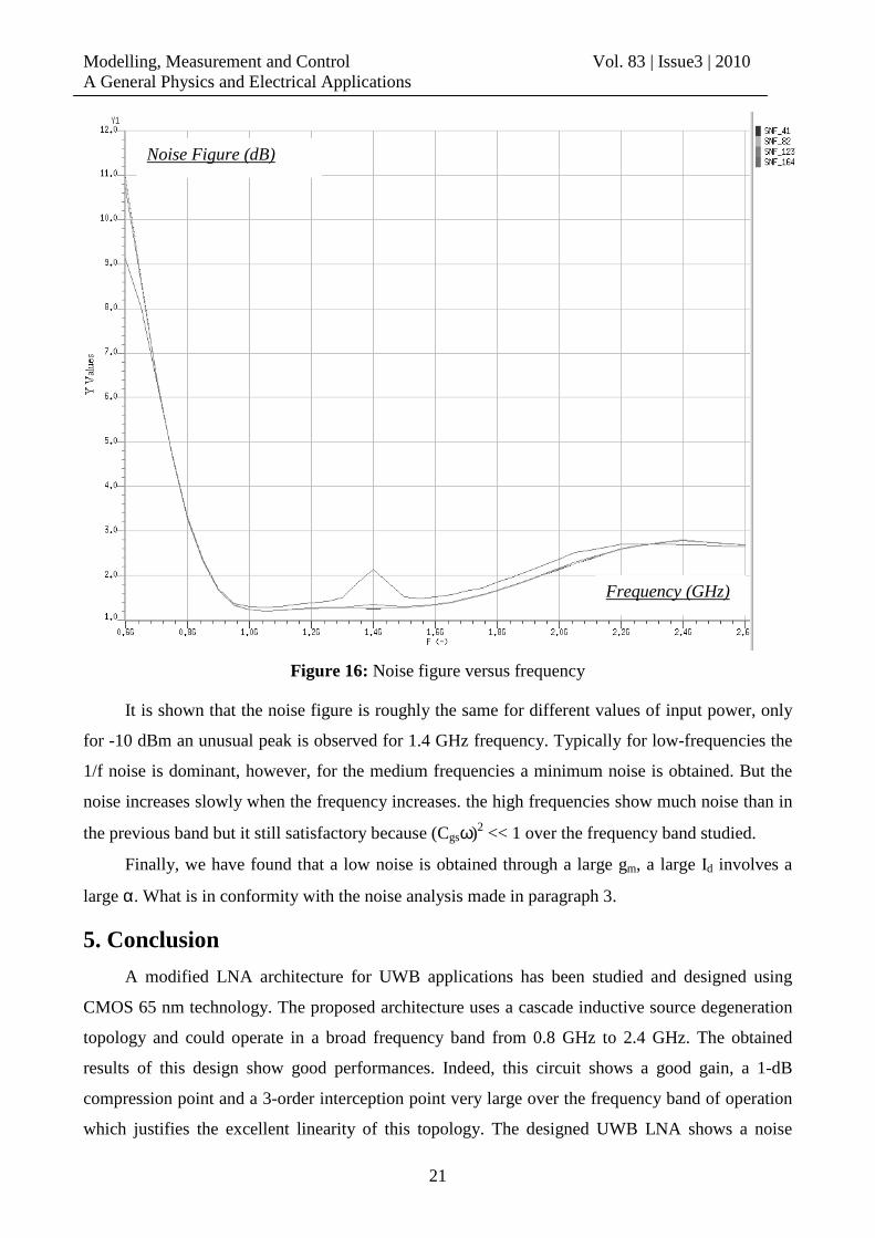
Figure 16 shows the noise figure of the UWB LNA over the frequency band from 0.6 to 2.6
GHz with various input power values ranging from -40 dBm to -10 dBm.
Frequency (GHz)
S11 parameter (dB)
S21 parameter (dB)
Frequency (GHz)
Modelling, Measurement and Control Vol. 83 | Issue3 | 2010 A General Physics and Electrical Applications
21
Figure 16: Noise figure versus frequency
It is shown that the noise figure is roughly the same for different values of input power, only
for -10 dBm an unusual peak is observed for 1.4 GHz frequency. Typically for low-frequencies the
1/f noise is dominant, however, for the medium frequencies a minimum noise is obtained. But the
noise increases slowly when the frequency increases. the high frequencies show much noise than in
the previous band but it still satisfactory because (Cgsω)2 << 1 over the frequency band studied.
Finally, we have found that a low noise is obtained through a large gm, a large Id involves a
large α. What is in conformity with the noise analysis made in paragraph 3.
5. Conclusion
A modified LNA architecture for UWB applications has been studied and designed using
CMOS 65 nm technology. The proposed architecture uses a cascade inductive source degeneration
topology and could operate in a broad frequency band from 0.8 GHz to 2.4 GHz. The obtained
results of this design show good performances. Indeed, this circuit shows a good gain, a 1-dB
compression point and a 3-order interception point very large over the frequency band of operation
which justifies the excellent linearity of this topology. The designed UWB LNA shows a noise
Frequency (GHz)
Noise Figure (dB)

Modelling, Measurement and Control Vol. 83 | Issue3 | 2010 A General Physics and Electrical Applications
22
figure equals to 1.4 dB and a good isolation lower than -10 dB with an acceptable power
consumption which not exceeds 29 mW.
References
1. W. Sansen, J.H. Huijsing and R.J. Van de Plassche, “Analog Circuit Design MOST RF Circuits,
Sigma-Delta Converters and Translinear Circuits,” Kluwer Academic Publishers, Netherlands,
pp. 3-20 and 121-126, 1996.
2. D. Leenaerts, J. van der Tang and C. Vaucher, “Circuit Design for RF Transceivers,” Kluwer
Academic Publishers, Boston, pp. 79-109, 2001.
3. A. Bevilacqua and A. M. Niknejad, “An Ulta widebande CMOS Low Noise Amplifier for 3.1 –
10.6 GHz Wireless Receivers,” IEEE J. Solid-State Circuit, vol. 39 no. 12, pp 2259-2268,
December 2004.
4. D. K. Sheffer and T. H. Lee, “A 1.5 V, 1.5 GHz CMOS low-noise amplifier,” IEEE J. Solid-
State Circuits, vol. 32, no. 5, pp. 745–759, May 1997.
5. J. Auvray, “Electronique des signaux analogiques,” Edition Dunod, pp. 121-128, 1980.
6. T. H. Lee, “The Design of CMOS Radio-Frequency Integrated Circuits,” UK Cambridge Univ.
Press, Cambridge, 1998.
7. D. K. Sheffer and T. H. Lee, “A 1.5 V, 1.5 GHz CMOS low-noise amplifier,” IEEE J. Solid-
State Circuits, vol. 32, no. 5, pp. 745–759, May 1997.
8. X. Fan, H. Zhang and E. Sánchez-Sinencio, “A Noise Reduction and Linearity Improvement
Technique for a Differential Cascode LNA,” IEEE Journal of Solid-State Circuits, vol. 43,
no. 3, pp. 588-599 March 2008.
9. L. Belostotski and J. W. Haslett, “Noise Figure Optimization of Inductively Degenerated
CMOS LNAs With Integrated Gate inductors,” Transactions on circuits and systems, vol. 53,
no. 7, pp. 1409-1422, July 2006.
10. M. Abdmouleh, “Design of 65nm CMOS Ring Oscillator with Low Phase Noise,” Final
Graduation Project, National Engineering School of Sfax, Tunisia, Septembre 2006.
11. C. Chung-Ping, Y. Cheng-Chi and C. Huey-Ru, “A 2.4~6GHz CMOS Broadband High-Gain
Differential LNA for UWB and WLAN Receiver,” Ref 0-7803-9162-4/05.IEEE,
pp. 469-472, 2005.
12. S. Lou, H.C. Luong, “A Linearization Technique for RF Receiver Front-End Using Second-
Order-Intermodulation Injection,” IEEE Journal of Solid-State Circuits, vol. 43, no. 11,
pp. 2404-2412, 2008.

Modelling, Measurement and Control Vol. 83 | Issue3 | 2010 A General Physics and Electrical Applications
23
13. H. Zhe-Yang, H. Che-Cheng, H. Yeh-Tai and C. Meng-Ping, “A CMOS Current Reused Low-
Noise Amplifier for Ultra-Wideband Wireless Receiver,” Ref 978-1-4244-1880-0/08 ICMMT
Proceedings, 2008.
14. T. Yao, et al., “Algoritmic Design of CMOS LNAs and Pas for 60-GHz Radio,” IEEE JSSC,
vol. 42, no. 5, pp. 1044-1057, May 2007.
15. C.H. Doan, S. Emami, A.M. Niknejad, R.W. Brodersen, “Millimeter-Wave CMOS Design,”
IEEE Journal of Solid-State Circuits, vol. 40, no. 1, pp. 144-155, 2005.
16. D. Zito, D. Pepe, B. Neri, T. Taris, J.-B. Begueret, Y. Deval, D. Belot, “A Novel LNA
Topology with Transformer-based Input Integrated Matching and its 60-GHz Millimeter-
wave CMOS 65-nm Design,” 14th IEEE International Conference on Electronics, Circuits
and Systems, Marrakech, Morocco, pp. 1340-1343, 2007.
17. F. Azevedo, F. Fortes, M. J. Rosário, “A New On-Chip CMOS Active Balun Integrated With
LNA,” 14th IEEE International Conference on Electronics, Circuits and Systems, Marrakech,
Morocco, pp. 1213-1216, 2007.
18. M. Rajashekharaiah et all, “A New Gain Controllable On-Chip Active Balun for 5GHz Direct
Conversion Receiver,” IEEE Trans. Microwave Theory Tech, vol. 50, no. 1, pp. 377-383,
January 2002.
19. H. Ta-Tao and K. Chien-Nan, “Low Power 8GHz Ultra-Wideband Active Balun,” SiRF press
2006, January 2006.
20. C. Vialon et all, “Design of an Original K-Band Active Balun With Improved Broadband
Balanced Bheavior,” IEEE Microwave and Wireless Comp. Letters, vol. 15, no. 4, pp. 280-
282, April 2005.
21. B. Welch, K.T. Kornegay, P. Hyun-Min, J. Laskar, “A 20-GHz Low-Noise Amplifier With
Active Balun in a 0.25-µm SiGe BICMOS Technology,” IEEE Journal of Solid-State
Circuits, vol. 40, no. 10, pp. 2092- 2097, 2005.