Design of a 10 kW Inverter for a Fuel Cell - search...
52
Design of a 10 kW Inverter for a Fuel Cell 2001 Future Energy Challenge Authors: Troy Nergaard, Jeremy Ferrell, Leonard Leslie, Brandon Witcher, Heath Kouns, and Dr. Jason Lai Submitted by: Virginia Tech Submitted on: June 15 th , 2001 Revised on: August 31 st , 2001
Transcript of Design of a 10 kW Inverter for a Fuel Cell - search...

Design of a 10 kW Inverter for a Fuel Cell
2001 Future Energy Challenge
Authors: Troy Nergaard, Jeremy Ferrell, Leonard Leslie, Brandon Witcher, Heath Kouns, and Dr. Jason Lai
Submitted by: Virginia Tech Submitted on: June 15th, 2001 Revised on: August 31st, 2001

VT 2001 FEC 2
Summary
The Virginia Tech Future Energy Challenge (FEC) Team has designed and built a 10-kW inverter
for a fuel cell system to enter into the 2001 Future Energy Challenge. The inverter accepts 48 V DC from a
fuel cell source and converts it to 120/240 V AC. This is accomplished by first using two full-bridge phase-
shifted converters and a multiple-output transformer to boost the low voltage to two split-200 V buses. The
split-200 V buses are the input to a half-bridge inverter, which creates the pulse width modulated (PMW)
sinusoidal output. A digital signal processor (DSP) is used for system control and to create the PWM signals
for the inverter. The fuel cell input is supplemented by a set of ultracapacitors, which help maintain bus
voltage during transients and start-up. A low-cost approach was used throughout the design and the price at
high quantity is projected to be under $500. However, it must be noted that low cost does not mean poor
performance; the efficiency of the inverter is around 90% at a 1.5 kW level. The unique features of the low-
cost design include:
1. Highly integrated system: The power stage, gate driver, auxiliary power supplies, sensors, and sensor
conditioning circuits are all integrated for both front-end DC-DC converter and DC-AC inverter.
2. Highly integrated circuit components: Many highly integrated commercially available ICs are used
to reduce the parts count. For example, (1) the entire front-end DC-DC converter is implemented
with a phase-shift modulation IC and a four-channel gate driver IC; (2) the inverter gate driver IC not
only performs device driving functions, but also provides protection and isolation; (3) the auxiliary
power supply ICs contain functions that include start up, PWM, high voltage MOSFET, over-current
protection, and over-temperature protection.
3. Discrete power components rather than power modules: The discrete power MOSFET and IGBT are
difficult to mount, but save substantial cost over their power module counterparts. Because the
power device is the major cost item in the system, the focus was on efficient utilization of power
devices and developing a unique mounting method with sufficient heat sinking capacity. Then
discrete power components can be used and the cost target can be met.

VT 2001 FEC 3
Table of Contents 1) INTRODUCTION ........................................................................................................................................................ 4
1.1) THE CHALLENGE ...................................................................................................................................................... 5 2) TEAM ORGANIZATION, MANAGEMENT, AND EDUCATIONAL IMPACT................................................. 5
2.1) TEAM ORGANIZATION .............................................................................................................................................. 5 2.2) MANAGEMENT ......................................................................................................................................................... 6 2.3) EDUCATIONAL IMPACT............................................................................................................................................. 6
3) SPECIFICATIONS ...................................................................................................................................................... 7
4) DESIGN......................................................................................................................................................................... 8 4.1) OVERVIEW ............................................................................................................................................................... 8 4.2) THEORY.................................................................................................................................................................. 10
Front End.................................................................................................................................................................. 10 Transformer .............................................................................................................................................................. 11 Inverter ..................................................................................................................................................................... 12 Output Filter ............................................................................................................................................................. 13 Sensing...................................................................................................................................................................... 13 Auxiliary Power Supplies.......................................................................................................................................... 15 Ultracapacitors......................................................................................................................................................... 16 Control ...................................................................................................................................................................... 17 Packaging ................................................................................................................................................................. 20
4.3) SIMULATION........................................................................................................................................................... 22 4.4) EXPERIMENTAL RESULTS ....................................................................................................................................... 26
5) COMPARISON .......................................................................................................................................................... 38
6) COST EVALUATION ............................................................................................................................................... 39 6.1) COST ANALYSIS ..................................................................................................................................................... 39 6.2) MANUFACTURABILITY ........................................................................................................................................... 42 6.3) RELIABILITY........................................................................................................................................................... 43
7) CONCLUSION ........................................................................................................................................................... 43
8) APPENDIX ................................................................................................................................................................. 45 8.1) CALCULATIONS ...................................................................................................................................................... 45 8.2) SIMULATION DIAGRAMS ........................................................................................................................................ 48 8.3) PRINTED CIRCUIT BOARDS..................................................................................................................................... 50
9) REFERENCES ........................................................................................................................................................... 51

VT 2001 FEC 4
1) Introduction
As the energy crisis around the world becomes more relevant, new renewable energy sources
become more enticing. One of these sources that has recently been revived and shows promising results for
applications as small as cellular phones to as large as utility power generation. This renewable energy source
is the hydrogen fuel cell. One particular interest for medium power fuel cell systems is distributed power
generation. Distributed power will allow the utility company to locate small, energy-saving units closer to
the customer [1]. It may even involve stand-alone systems for residential use. A block diagram of a fuel cell
system used for stand-alone or utility connect is shown in Figure 1.
Fuel CellLoad/Grid
Battery/UltraCap
DC/DCConverter
DC LinkCap Inverter
Figure 1. Block Diagram of Fuel Cell System
Fuel cells are an environmentally clean, quiet, and an efficient method for generating electricity. A
fuel cell is an electrochemical device that converts chemical energy of fuel directly to usable energy without
combustion. Often a hydrogen-rich fuel, typically natural gas or methanol, is first reformed into hydrogen.
The hydrogen is sent to the fuel cell where it combines with oxygen to produce electricity and water. Fuel
cells, themselves, are very complicated structures, which introduce many design challenges into the system.
More often than not, fuel cells require some type of power conditioning circuit to be useful. The power
conditioning circuit is shown in the blue, dashed box above. Currently, the cost of fuel cell systems is high,
which limits their popularity and availability. In order to make use of this clean energy, much work must be
done to reduce the price and increase the reliability.

VT 2001 FEC 5
1.1) The Challenge
The Future Energy Challenge (FEC) is a student competition whose goals are to design and build a
low-cost, efficient inverter for a 48-volt fuel cell application. Fourteen universities from across the country
will compete in this year’s challenge, which is sponsored by US Department of Energy, the National
Association of State Energy Officials, the Institute of Electrical and Electronic Engineers, and the
Department of Defense.
2) Team Organization, Management, and Educational Impact
2.1) Team Organization
Virginia Polytechnic Institute and State University (VT) has formed a multi-disciplinary team
consisting of ten students and three faculty advisors. The students are divided into seven main groups and
overseen by a student team leader. The three faculty advisors are specialized in (1) power electronics, (2)
fuel cell and thermal management, and (3) energy and power systems. The seven student groups are divided
into (1) auxiliary power supplies, (2) inverter and gate drivers, (3) front-end DC-DC converter, (4) case and
heat sink, (5) DSP and PWM control, and (6) sensor, conditioning, and interface. Each group was
responsible for the design and simulation verification of their section. The team leader coordinates all the
technical efforts, participates in some of the key designs, and leads in system integration and testing. An
organizational chart is shown in Figure 2. This chart lists all of the members of the team who helped VT
complete the FEC requirements.

VT 2001 FEC 6
Faculty AdvisorsDr. Jason Lai (ECE)Dr. Doug Nelson (ME)Dr. Lamine Mili (ECE)
Team Leader and System IntegrationTroy Nergaard (ECE, G)
Auxiliary Power SuppliesRobert Gannett (ECE, G)Mike Pochet (ECE, UG)
Inverter and Gate DriversJeremy Ferrell (ECE, UG)Tom Shearer (ECE, UG)
Front-End DC-DC ConverterLeonard Leslie (ECE, UG)Troy Nergaard (ECE, G)
Case and Heat SinkHeath Kouns (ECE, G)Steve Gurski (ME, G)
DSP and PWM ControlHeath Kouns (ECE, G)Leonard Leslie(ECE, UG)
Sensor, Conditioning, and InterfaceBrandon Witcher (ECE, UG)John Reichl (ECE, UG)
Figure 2. VT FEC Team Organization Chart
2.2) Management The Virginia Tech FEC team held weekly meetings with all of its members to discuss the interaction
and relevant timing of the project. The first person listed in each group took the lead in technical design and
sought help from other members when necessary. Faculty advisors provided appropriate guidance in
technical directions and sought funding sources for expenses in parts and travel. The entire system was
designed, built, and tested by the student team members.
2.3) Educational Impact All electrical and computer engineering (ECE) students on the team received credits in senior
electronic design courses (ECE 4205 and 4206) that involve design, simulation, fabrication, and testing of
power supplies and inverters. The ECE 4205 emphasizes theoretical analysis and design, and ECE4206 is a
senior capstone course that allows students to work on special projects. All of our ECE team members took
one or both of these courses and were interested in participating in the Future Energy Challenge Competition.
All team members volunteered to be part of the competition.

VT 2001 FEC 7
This competition not only helps promote and implement alternative energy sources, it also introduces
students to the power electronics field and gives them an excellent opportunity to apply what they learn in
the classroom to a real engineering project. Perhaps the most significant impact from a societal point of view
is the creation of well-educated power electronics engineers. Through this competition, all the team
members felt that they learned practical application of classroom material and are now better prepared for
their future careers in the power electronics area.
The success of the VT FEC team from an educational standpoint can be found in the number of
students joining the graduate program in power electronics. In Fall 2000, this competition attracted three
graduate students, Troy Nergaard, Heath Kouns, and Robert Gannett, who came from ECE 4205 and 4206
courses. In Spring 2001, four team members applied for the graduate program and will become graduate
student in the Fall of 2001: they are Leonard Leslie, Jeremy Ferrell, Brandon Witcher, and John Reichl.
3) Specifications
The main goal of the 2001 Future Energy Challenge was to design a 10 kW inverter at a minimum
cost, yet still maintain acceptable levels of performance, reliability, and safety. The schools were allowed to
demonstrate their concept by building a scaled inverter that could be powered by a 1.5 kW fuel cell. The
specifications for the 10 kW system are shown in Table 1.
Table 1. Design Specifications
Parameter Target Requirement Output Power Capability
10 kW continuous, Single-phase 120/240 V, 60 Hz output suitable for domestic applications
Input Source 48 V DC nominal source (tolerance range 42 V- 72 V) with slow transient characteristics.
Manufacturing Cost $500 maximum when scaled to a 10kW design in high volume production Package Size Volume less than 50L Package Weight Mass less then 32 kg, not including energy sources or batteries Overall Efficiency Higher then 90% for 10 kW resistive load Total Harmonic Distortion
Output voltage: less than 5% when supplying a standard nonlinear test load
Safety The system is intended for safe, routine use in a home or small business by non-technical customers.
Voltage Regulation Output voltage tolerance no wider than ±6% over the entire line voltage and temperature range, from no-load to full-load. Frequency 60±0.1 Hz.

VT 2001 FEC 8
Acoustic Noise No louder than conventional domestic refrigerator. Less than 50 dBA sound level measured 1.5 m from the unit.
Electrical Noise Able to meet FCC Class A--industrial requirements for conducted and radiated EMI.
Protection Self-protection against output short circuit, over current, over temperature, over voltage, and under voltage or loss of input source with no damage caused by any of these.
Environment Suitable for indoor installation in domestic applications, 10°C to 40°C possible ambient range.
Lifetime The system should function for at least ten years with routine maintenance when subjected to normal use in a 20°C to 30°C ambient environment.
4) Design
4.1) Overview
The VT Team designed and built a complete 10 kW inverter system. The team decided that building
a smaller prototype was not an accurate assessment of the larger design. The design emphasis was on
integration and cost reduction, but without sacrificing performance. The entire electrical and mechanical
design was done in-house; from the auxiliary power supplies to the gate drive circuit to the power stage.
Even the Printed Circuit Boards (PCBs) were designed entirely by the students.
A detailed topology evaluation was done to find the optimum converter from a cost standpoint. The
goal was to minimize the number of components and choose devices that were highly integrated and low in
cost. Manufacturability also played a major role in the overall design. Several topologies for the DC-DC
converter were considered, including push-pull, half bridge, and full bridge. At a 10 kW level, the full bridge
topology was determined to be the most practical.
The system developed, consists of three main sections: two full bridge DC-DC converters (front
end), two half-bridge inverters, and the DSP control. A block diagram of the VT design is shown in Figure
3. The front-end section is a full bridge, phase-shifted, PWM controlled DC-DC converter. Adding a
transformer allows the 48 volts from the fuel cell to be boosted to two split 200 V DC buses for the DC link
to the inverter. The split 200 V DC buses are both well regulated by the front-end converter and are different
from splitting two voltages from one 400 V bus with bulk capacitors. This design allows full utilization of
600 V IGBTs, reduces device and associated component counts, and minimizes device losses. The major

VT 2001 FEC 9
challenge in this design is how to achieve low-leakage inductance from a multiple tapped high frequency
transformer. The inverter section takes the output of the transformer, rectifies it, and then filters it into high
voltage DC so that it can be inverted to 120 volt, 60 Hz AC. There are two 120-volt inverters, operating at
180° out of phase so that they can be connected together for a 240-volt output. An Analog Devices DSP
evaluation board is used to generate the PWM signals for the inverters, to generate the control signals for the
front end, and to do system level control including fuel cell and user interface communication.
Full BridgePhase
Shifted FrontEnd
UltraCap
Transformer
Half BridgeInverter
Half BridgeInverter
Filter
Filter
120 Vac
120 Vac240 Vac
Rectifierand DC
Link
Rectifierand DC
Link
48 Vdc
DSP Control
Full BridgePhase
Shifted FrontEnd
Figure 3. Block Diagram of Inverter System
There are many features of the system, but probably the most impressive is the integration. There
are three PCBs that make up the entire system. The only connections that are necessary, besides input and
output, are from front end to the transformer, from transformer to the inverter, and then a few plug-in cables
from the control board to each of the other boards. The auxiliary power supplies, gate drives, sensing
circuits, and filters are completely integrated into the power stage boards. The main transformers are planar
and consist of PCBs that drop directly into the core. This provides complete isolation from input to output
and from power to control. A complete list of the features is shown in Table 2.
Table 2. Features of System
Feature Description Output Power 10 kW continuous, Single-phase 120/240 V, 60 Hz output Integration Sensors, gate drivers, power stage, and filters are integrated into PCB Isolation Complete isolation between input and output and between power and
control. Soft Switching Capability
Devices on front end can achieve zero voltage switching at heavy load with no added components.

VT 2001 FEC 10
Completely enclosed All of the components, including the heat sinks are enclosed in a metal case.
Soft Start The system can limit inrush current from the fuel cell and slowly charge up the internal DC bus.
Ease of Manufacturability
Minimum number of physical connections, no winding of transformer necessary.
Simple Interface Two switches, three LED indicators and a RS-232 port for diagnostics and programming.
Protection Protection against input under and over voltage. Desaturation protection via inverter gate drivers for output short circuit protection.
An electrical schematic of the entire power stage is shown in Figure 4.
Vfc
Q1
Cdc1D2
Q2
D1 Ldc1
Vac1
Q3
Q4
X1
Cdc2Ldc2
Vac2
Cin1
D4
D3
Cdc3
D6
D5 Ldc3
Cdc4Ldc4D8
D7
IGBT1
IGBT2
Lo1
Co1
IGBT3
IGBT4
Lo2
Co2
Q5
Q6
Q7
Q8 X2
Cin2
Figure 4. Power Stage Schematic
4.2) Theory
Front End As mentioned previously, the front end consists of a phase-shifted full bridge circuit. A schematic of
this topology is shown in Figure 5 below. Given the low input voltage and high input current, the device of
choice is the MOSFET. Therefore, MOSFETs rated at 75 volts, 148 amps, and having a low on resistance
were chosen. Specific part numbers of all components can be found in Table 5 under the cost analysis
section. A single Intersil HIP4081A, which uses a bootstrap supply, provides the gate drive for the
MOSFETs. The phase-shifted control is done with the UC3895 from Texas Instruments. Device pairs Q1

VT 2001 FEC 11
and Q2 are complementary and Q3 and Q4 are complementary, which allows for one leg to be phase shifted
resulting in a varying duty cycle. The phase shifted full bridge topology allows the leading phase leg
switches to turn on under zero voltage conditions for most loads. The lagging leg switches can also achieve
zero voltage switching (ZVS) under heavy load conditions; ZVS reduces the losses in the switches,
increasing overall system efficiency. The UC3895 provides an error amplifier for the voltage control
compensator. Over current protection for the front end is provided by the control chip. Also, shown in
Figure 5 are two high frequency, polypropylene capacitors across the input bus. These are located as close to
the devices as possible so to minimize the inductance and keep the voltage overshoot low.
D2
D1
X1
Cin15 mF
D4
D3
Chf1 Chf2
Q3
Q4
Q1
Q2
Vdc48 V
Figure 5. Front End Circuit
Transformer The full bridge circuit creates a quasi-square wave for the primary of the transformer. The input is
boosted and then full bridge rectification takes place via a center tap and two diodes. Given a minimum
input voltage of 42 volts, the output of each half bridge inverter is required to be 120 volts rms, and the loss
of effective duty cycle due to leakage inductance in the transformer, the transformer turns ratio can be
determined to perform correctly at 85% modulation index. With the cores available, two turns on the primary
were necessary, so the final turns ratio is 2:13. This ratio corresponds to (2) and allows for some losses in
the circuit.
VModIndexVV ac
dc 4002*max
min == (1)
168.0*5.0
*
min
min ==dc
lossin
VDV
N (2)

VT 2001 FEC 12
The transformer looks quite complicated and unique, but is made out of a simple ferrite planar core
and a 14-layer printed circuit board. The planar windings are interleaved to reduce the leakage inductance
and therefore reduce the duty cycle loss of the front end that is associated with the charging of the leakage
inductance. The single input is actually transformed into two sets of center-tapped windings acting as though
there were two separate voltage sources. The center tap also allows a minimum number of rectifier diodes to
be used. This device must be fast recovery, so a Hexfred device from IR is used. After the rectification, the
full wave rectification is filtered through an inductor and a capacitor to create a 400 V DC bus.
Inverter The inverters are half bridge topologies utilizing a split capacitor bus. As mentioned above,
however, this split bus is not like the typical half bridge configuration powered by one source. Because of
the way the transformer was designed, the capacitors do not divide the source in half. This prevents any
imbalance issues and helps reduce the number of components needed. The LC filter used after the rectifier
was designed with a low cutoff frequency in order to minimize the ripple on the DC link. The inductor was
also designed with optimum operation of the front-end DC-DC converter in mind.
The voltage is larger on the secondary side, so IGBTs were chosen to meet this criterion and again
devices from IR were used. These IGBTs are extremely fast and capable of 60 amps of continuous current.
The gate drive circuit uses a very functional integrated circuit, HCPL316J, which provides sufficient driving
current and optical isolation for both input and fault signals. Because of the high current output capability the
output of the drive chip can directly drive the IGBTs without an extra driving stage. The HCPL316J gate
driver chip provides de-saturation (de-sat) protection when the device is over current or short-circuited. The
de-sat function reduces the gate drive power supply to zero so that the device turns off when the voltage
exceeds a limit, which is typically caused by over-current or short circuit. The turn-off action does not need
to go through logic or the DSP, and as a result, trips the device on a micro-second time scale so that the
device will always be saved. With such fast protection, the unit will not fail even with the inverter output
short-circuited.

VT 2001 FEC 13
Output Filter The PWM output from the IGBT half-bridge is then filtered using an inductor and a capacitor to get
a sinusoidal output. It is desired to have the cutoff frequency of the filter around 1 kHz to eliminate high
frequency switching ripple, yet still maintain reasonably sized components. It is also very important to have
the characteristic impedance of the filter match the load impedance, so that the inrush current to the filter
capacitor is limited. Using (3) and (4), the filter component values can be selected and the inductor can be
designed.
kHz 12
1 ≈=oo
c CLf
π
(3)
Ω=== 88.25_ kWLo
oo R
CL
Z (4)
The output inductors were designed using high permeability Kool Mu cores and careful
consideration was taken to avoid saturation. The core loss is minimal because the fundamental frequency is
60 Hz. Figure 6 shows the two inverters with the output filters values.
Cdc12.2m
Vac1120 V
Cdc22.2m
Vac2120 V
IGBT1
IGBT2
Lo1330 uH
Co140 uF
IGBT3
IGBT4 Lo2330 uH
Co240 uF
Cdc32.2m
Cdc42.2m
Chf3
Chf4
Vac3240 V
Figure 6. Inverter Circuit
Sensing Sensing circuits were designed to feedback all of the necessary information for system control. The
front end PCB has fuel cell voltage and input voltage sensing information integrated onto it. Integrated onto

VT 2001 FEC 14
the inverter board are sensing circuits for both DC link voltages, both AC output voltages and both AC
output currents. All of these sensing circuits are designed for low cost and are isolated from the power stage.
The AC voltage sense circuit consists of two gain stages, an offset stage, an isolation stage, and a
filtering stage. The circuit is shown below in Figure 7. The first gain stage is a voltage divider at each of
the terminals of the output voltage. The second gain stage is an instrumental amplifier (IA), which was
utilized for its high common mode rejection characteristic. The output of the IA is sent to the offset stage,
which is necessary because the isolation stage will clip negative voltage. The next stage provides isolation
between the high voltage circuitry and the circuitry on the control board. This stage consists of a voltage-to-
current converter to interface the voltage gain and offset stages to the HCNR201 (a linear optocoupler) and a
current-to-voltage converter to translate the current out of the optocoupler back to voltage. The last stage is a
4th order, 3 dB Chebyshev filter. The filter is designed so that there is less than 3º of phase shift at 60 Hz and
better than 80 dB of attenuation at the inverter stage switching frequency (24 kHz). Since the A/D voltage
range is –2 to 2 V, the previously created offset is nullified via a capacitor that couples the output of the AC
voltage sense circuit to the A/D input.
The operation of the DC link voltage sense circuit and the fuel cell voltage sense circuit is very
similar to that of the AC voltage sense. Again, there are gain stages, filtering stages, and isolation stages.
The front end of the sense circuit also contains a common mode filter for both the positive and negative legs
of the differential input, as well as a differential mode filter. The common mode filter has a cutoff frequency
of 3 kHz (one decade below the DC-DC converter switching frequency), and the differential filter has a
cutoff of 600 Hz (two decades below the ripple frequency). For the DC bus voltage, phase shift is not a
concern, so passive filtering at the input can easily be implemented and should aid circuit performance.
Again, the HCNR201 is utilized to provide isolation with the help of a V-I converter and an I-V converter.
After the isolation stage the overall gain of the circuit is 0.004 V/V. The last stage of the circuit is a simple
KRC filter. This filter will further reduce the noise injected at the input and any noise picked up by the wires
connecting the inverter board (where most of the DC link sense circuit will be) and the control board (where
the filter will be) before allowing the signal to reach the A/D. Again, this filter will reduce the noise to well

VT 2001 FEC 15
below the resolution of the A/D, meaning that there will be better than 80 dB of attenuation before the
switching frequency of the DC-DC converter (24 kHz).
The output current is measured via a current transformer whose primary winding is in series with the
load. The secondary of the CT is terminated via a small resistor to convert the signal to voltage, and a simple
op amp gain stage is used to set the overall circuit gain to 0.03 V/A. Again, filtering will be used to reduce
the noise seen by the A/D.
+15
AC
To ControlBoard
HCNR201
LM833LM833
LM833
IA
Figure 7. AC Voltage Sensing Circuit
Auxiliary Power Supplies Small auxiliary power supplies are integrated onto each of the main boards. Because a highly
integrated controller chip is used, these supplies are simple, inexpensive, and produce about 10 W. The
auxiliary supplies are used to provide power to the gate drivers, control chips, and sensing op amps. The
design utilizes a TOPswitch that combines start-up, PWM regulator, power MOSFET, internal
compensation, and protection. Therefore, it allows minimum parts count for low-cost manufacturing. This
auxiliary power supply chip is protected against over current and over temperature. To provide proper
isolation, three power supplies had to be created. All three operate from the 48 volt input bus, which allows
the entire system to function before power is drawn. Each of the supplies begins to operate, and is regulated,
at approximately 60% of the voltage. This allows all of the chips to be operating before full voltage is
applied and the DSP to start regardless of the initial ultracapacitor voltage. A schematic of one of the
auxiliary power supplies is shown in Figure 8.

VT 2001 FEC 16
D10
D13
D15
D14
D11
TL431
D12
C14 C15
C16 C17
C18 C19
R11
R12
R13
R10
C10
C11
C12
C13
DC+
DC-
+15
15COM
-15
+12
12GND
TOPswitchD
S
Figure 8. Auxiliary Power Supply
Ultracapacitors The fuel cell requires some type of backup during start up and transient conditions. Typically a
battery is used, but often requires additional circuitry for charging and state-of-charge monitoring. These
additional circuits consume space and add cost to the system. Ultracapacitors are another option that can be
paralleled with the fuel cell with little or no additional circuitry. This will reduce the part count and increase
the reliability of the system. Ultracapacitors across the input bus also allow for easy start-up without the fuel
cell being online. In this design, ultracapacitors are capable of holding charge over long periods of time and
can be used as the supplementary power source.
Wh55.0 Ws10*98.1* 3 === −− upstartupstart tPE (5)
Wh121 Ws10*36.4 55
010_10 ==∆= ∫
−ττ dtePEt
kWtransientkW
(6)
Wh18 Ws10*56.6 45
05.1_5.1 ==∆= ∫
−ττ dtePEt
kWtransientkW
(7)
Assuming the time response of the fuel cell is 40 seconds, the max energy required during transients
is shown in (6). The ultracapacitor bank needed for the 10 kW design is 440 kJ, which will allow the system
to be started off of the ultracapacitors and run at least 90 seconds until the fuel cell is ready. The
ultracapacitors will also provide energy when transients occur and when the fuel cell is in transition. The

VT 2001 FEC 17
four ultracapacitors that are integrated in this system are sized for a 3 kW system, and are 13 V and 35 kJ per
module. This gives a total of 38 Wh and easily meets the criteria given in (7). The ultracapacitor bank is
limited to a peak voltage of 56 volts, so if the input voltage is on the high end (light load condition) the
ultracapacitors will be switched out of the circuit.
Control The control for the entire inverter system is done with the Analog Devices ADMC401 DSP. The
ADMC401 is a 26 MIPS, fixed-point processor. This DSP chip has six PWM signals available, 12 general-
purpose I/O pins, and 8 analog to digital inputs.
As mentioned above, the phase shift control of the front-ends are performed by Texas Instruments’
chips. The control loop for the front-end was designed using a small signal model developed for this
topology by Tsai [3]. The control loop is implemented with a digital PI compensator in the ADMC401. The
input to the control loop is the error between a reference and the sensed DC link voltage. The output of the
control loop is sent to the digital to analog converter (DAC) on the control board. The output of the DAC is
sent to the UC3895, which uses the 0-5 volt signal to determine the required phase shift for the front-end
converter. By having a separate front-end converter for each of the inverters, the problem of controlling the
DC link voltage when the system is under unbalanced load conditions is eliminated.
The two inverters are controlled entirely by the DSP. Again the output voltage is fed back to the
DSP and a sine wave reference is subtracted from it. This error signal is input into a PI compensator and
then written to the PWM generator. Four sinusoidal PWM signals are generated and sent to the gate drivers.
The DSP will also adjust the modulation index of the two inverter legs to keep the output voltages regulated
under unbalanced load conditions. An interface board was designed to integrate the DSP with the entire
system. It has its own ±5/±15 volt isolated power supply for the DSP, filters, and drivers.

VT 2001 FEC 18
Control Board
Fuel CellUltraCaps
DSPAuxSupply
SmallUltraCaps
Front End Board Inverter Board
AuxSupply
On Off
Figure 9. Control Diagram
From a system standpoint, the DSP board is in complete control. A small PCB interfaces the DSP
with the rest of the system, filters the A/D inputs, and buffers the digital outputs. All of the sensing
parameters are sent back to the DSP and are monitored for control and for fault conditions. If a fault is
detected by the DSP from the IGBT gate drivers, it will try to restart twice more to make sure it wasn’t noise,
and then it will immediately shut down the inverter and front-end stages and light up the fault LED. It will
also send a signal to the fuel cell indicating no power is needed. Finally, it will turn on the coil to the
normally closed relay in the path with the switch, which will open that path and effectively cause the DSP to
turn the power off on itself. An overview of the system control is shown in Figure 9, where all of the blue
arrows represent control data.
The external communication between the fuel cell and the inverter will be done by the DSP. When
the switch on the front panel is pressed on, the relay will close bypassing the switch and the switch can be
released. The DSP will then power up off of the ultracapacitor and will immediately send a digital signal to
the fuel cell telling it to turn on. Then a power request will be sent to the fuel cell and it will send back a
power available signal. With the ultracapacitors in parallel with the fuel cell, the power available signal can
be ignored and power control is extremely simple. Initially, the inrush current to the inverter could cause an
over current fault in the fuel cell. To avoid this condition, the inverter will soft start the fuel cell by allowing
the current to flow through a power resistor in the circuit. When the fuel cell voltage and the ultracapacitor
voltage match, the relay will be closed and the resistors will be bypassed. Next the front-end will be enabled
VT 2001 FEC 19
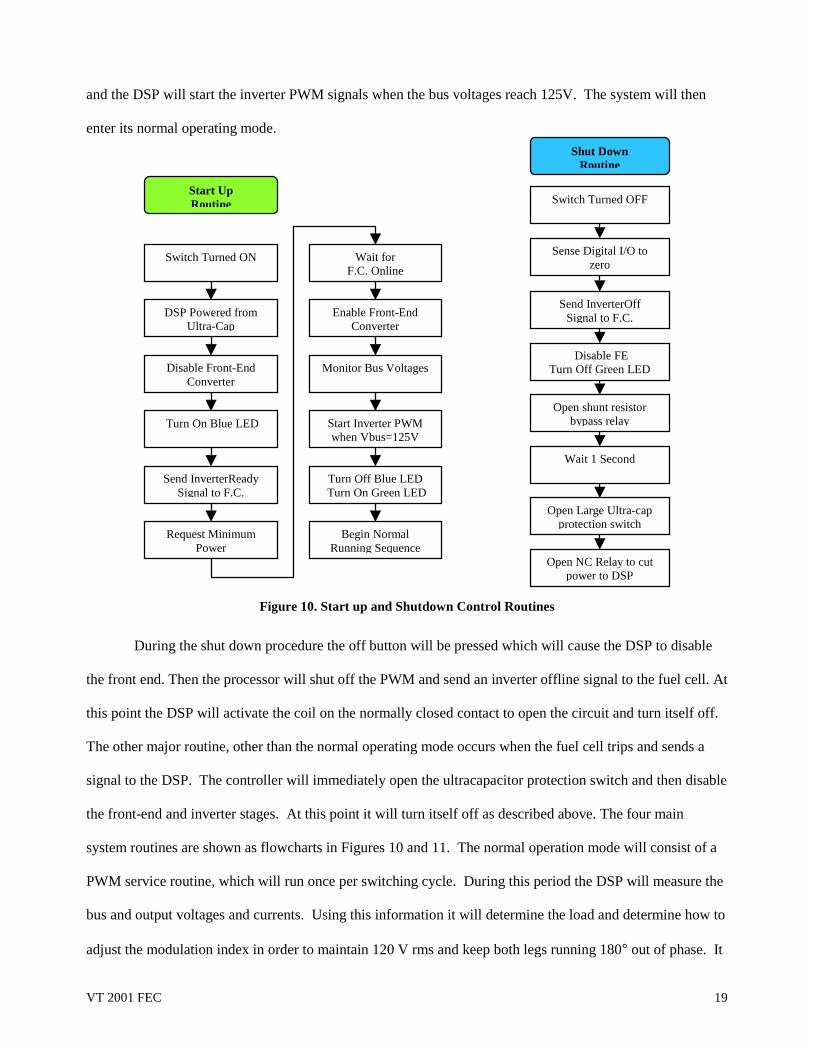
and the DSP will start the inverter PWM signals when the bus voltages reach 125V. The system will then
enter its normal operating mode.
Figure 10. Start up and Shutdown Control Routines
During the shut down procedure the off button will be pressed which will cause the DSP to disable
the front end. Then the processor will shut off the PWM and send an inverter offline signal to the fuel cell. At
this point the DSP will activate the coil on the normally closed contact to open the circuit and turn itself off.
The other major routine, other than the normal operating mode occurs when the fuel cell trips and sends a
signal to the DSP. The controller will immediately open the ultracapacitor protection switch and then disable
the front-end and inverter stages. At this point it will turn itself off as described above. The four main
system routines are shown as flowcharts in Figures 10 and 11. The normal operation mode will consist of a
PWM service routine, which will run once per switching cycle. During this period the DSP will measure the
bus and output voltages and currents. Using this information it will determine the load and determine how to
adjust the modulation index in order to maintain 120 V rms and keep both legs running 180° out of phase. It
Shut Down Routine
Switch Turned OFF
Send InverterOff Signal to F.C.
Open shunt resistor bypass relay
Wait 1 Second
Open Large Ultra-cap protection switch
Disable FE Turn Off Green LED
Open NC Relay to cut power to DSP
Sense Digital I/O to zero
Start Up Routine
Switch Turned ON
DSP Powered from Ultra-Cap
Send InverterReady Signal to F.C.
Request Minimum Power
Wait for F.C. Online
Enable Front-End Converter
Monitor Bus Voltages
Start Inverter PWM when Vbus=125V
Begin Normal Running Sequence
Turn Off Blue LED Turn On Green LED
Turn On Blue LED
Disable Front-EndConverter

VT 2001 FEC 20
will also look at communication signals and determine if any corrective action should occur. If the load has
changed, the processor will send the correct power request to the fuel cell. If a fault is observed then the unit
will enter one of the special modes shown in Figure 11.
Figure 11. Fault Control Routines
Packaging
Packaging of power electronic circuits is a feature that can easily be overlooked. This is a major
source of cost and complication in a system if it is not addressed correctly. Virginia Tech’s system was
designed to minimize manual labor required to construct the unit and to reduce cost. Cooling and layout are
two areas that must be looked at to obtain an effective design.
Three heat sinks are necessary to keep the device temperatures at an acceptable level. The heat sinks
are sized assuming 90% overall efficiency at 10 kW, so each heat sink should dissipate approximately 300
Inverter Fault Routine
Detect Gate Drive Fault
Let Inverter Operate
Send Minimum Power Request
Send Inverter Off Signal
Disable Front-End Converter
Reset Gate Drive Chip
Check Fault Signal
Continue Normal Operation
Open shunt resistor bypass relay
Open Large Ultra-capprotection switch
Wait 20 seconds
Turn Off Green LED Turn On Red LED
Open NC Relay to cut power to DSP
Fuel Cell Trip Routine
Receive F.C. Trip Signal
Turn Off Green LED Turn On Red LED
Turn Off Inverter PWM
Open Large Ultra-capprotection switch
Wait for DC Bus voltage < 50
Wait 20 seconds
Disable Front-End Converter
Open NC Relay to cut power to DSP
Let Inverter Operate
Reset Gate Drive Chip
Voltage Fault Routine
DC Bus > 500 V or F.C. voltage < 42 V
Turn Off Green LED Turn On Red LED
Turn Off Inverter PWM
Open Large Ultra-cap protection switch
Wait for DC Bus voltage < 50
Wait 20 seconds
Disable Front-End Converter
Open NC Relay to cut power to DSP

VT 2001 FEC 21
watts. Three small fans are added to keep air flowing throughout the enclosure and to provide a minimum
load to the system.
Figure 12. Physical Layout
A CAD representation of the entire inverter system without the ultracapacitors is shown in Figure 12.
There are three large input connections for the fuel cell and the ultracapacitor. These are water tight and
capable of accepting a standard #4 AWG wire. There is also a six-pin signal connector that goes to the fuel
cell for communication purposes. Located on the side of the box are three LEDs that indicate the status of
the system. Separate on and off buttons are also located on the side for easy access. There is a RS-232 port
available for communicating with the DSP. The output consist of two NEMA 5-15R standard 120 V and one
NEMA 6-15R standard 240 V receptacles, both of which are fused accordingly.
The package was designed assuming assembly line construction techniques will ultimately be used to
build the unit. First, the fans and receptacles will be attached to the base and the cabling will be run. Then
the front-end board and inverter board would be attached to their respective heat sinks. Both boards will be
dropped into the base of the unit and attached from the top to brackets, and then bolts would be added
through the bottom of the case into the heat sinks to hold everything secure. A plate will be attached

VT 2001 FEC 22
between the front-end board and inverter board and the transformer will be bolted in place. Next, the pre-
assembled wiring harness will be connected and the top of the case will be secured. Because of the high level
of integration and the ability to pre-assemble the separate boards, the manual labor to construct the unit is
minimized. Minimizing labor leads to lower prices for the customer. Also, because PEM style fasteners
were used and holes were tapped in the heat sink, bolts with captive washers can to be screwed in with an
electric nut driver to speed assembly.
4.3) Simulation
After completing the theoretical design, the power stage of the system was simulated using Saber in
order to verify the design. The simulation schematics are shown in the appendix. The system was simulated
under several different load conditions and input voltages. Some of the system output waveforms are shown
below. Initially, an ideal voltage source was used as the fuel cell. The system was simulated using ideal
switches and an ideal transformer. Small parasitic components were inserted in the system to make it more
realistic.
Figure 13. 120 V Output Waveforms at Full Load

VT 2001 FEC 23
Figure 14. 240 V Output Waveforms at Full Load
As shown from Figure 13 and Figure 14, the simulations verify the design and produce 120 and 240
Vac output. All of the device currents and voltages were also simulated to make sure the component choices
were the correct ones. The efficiency was also calculated using the 10 kW simulation, shown in Figure 15,
and was determined to be about 85%. There is a large ripple on the input current, which may be eliminated
with the addition of the ultracapacitors. Therefore the efficiency could be slightly higher than 85%.

VT 2001 FEC 24
Figure 15. Efficiency of System at 10 kW
To help verify the effect of the fuel cell on the system, a simple model of the 1.5 kW fuel cell was
developed using the V-I curves supplied by NETL [2] and assuming a fuel utilization of about 70%. This
curve is shown below and is used in the fuel cell model created in Saber.
V-I Curve for 1.5 kW Fuel Cell
0
10
20
30
40
50
60
70
0 10 20 30 40 50 60 70Current (amps)
Volta
ge (v
olts
)
Figure 16. Fuel Cell Characteristic at 70% H2 Utilization

VT 2001 FEC 25
A simulation was run with the fuel cell model and the ultracapacitor to verify transient behavior.
The circuit used was simplified for convergence reasons, and is shown in the Appendix. Figure 17 shows
that when a load is increased, and the fuel cell can not provide enough power the ultracapacitors will do a
sufficient job to provide the rest of the power until the fuel flow can be increased.
Figure 17. Fuel Cell and Ultracapacitor Transient Simulation
The control loop of the full bridge phase shifted converter was simulated in PSPICE using a small
signal model [3] for the full bridge circuit. The simulation circuit is shown in the appendix and the Loop
Gain Bode Plot is shown in Figure 18.

VT 2001 FEC 26
Frequency
10mHz 1.0Hz 100Hz 10KHz 1.0MHz1 DB(V(DRETURN)/V(D)) 2 P(V(DRETURN)/V(D))
-100
-50
0
50
1001
0d
40d
80d
120d2
>>
(614.415,102.982)
(614.415,61.210m)
Figure 18. Front-End Loop Gain Bode Plot
With the compensator designed, the loop gain bode plot exhibits a phase margin of 102° and a gain margin of
about 60 dB. Since the front-end control does not need to be very fast, a crossover frequency of 614 Hz is
acceptable.
4.4) Experimental Results
A picture of the 10 kW prototype inverter on a test bench is shown in Figure 19. The fuel cell input
would be on the left and the 120 V/240 V outputs are on the right. Since a fuel cell was not available, this
system was tested with a DC power supply as the input source. The unit was tested open loop and closed
loop, using the DSP for PWM generation, at several different load conditions and input voltages. Resistive,
inductive, rectified, and unbalanced loads were used and the waveforms are shown on the previous pages.
Load steps were also performed to evaluate transient response. Using a balanced resistive load, the efficiency
of the unit was measured over the range of 300 W to 3.2 kW and the results are shown in Figure 20.

VT 2001 FEC 27
Figure 19. Prototype Inverter System
Because this is a 10 kW inverter, the efficiency will be lower at loads between 300 W and 1 kW.
These are only 5% to 10% of rated load, so the front end runs in discontinuous mode and the switching loss
plays a major role in the overall power loss. Also the duty cycle of the front-end is low, so the circulating
current is large.
10 kW Inverter Efficiency at Light Load
70
75
80
85
90
95
0 500 1000 1500 2000 2500 3000 3500Total Power(W)
Effic
ienc
y(%
)
Figure 20. Efficiency Curve

VT 2001 FEC 28
Figure 21 and Figure 22 show the output voltage and current waveforms at different load conditions.
The current is the light green color (number 3) and 1 volt is equal to 1 amp. The waveforms clearly show
that the system operates at 120 and 240 volts.
Figure 21. 120 V Output Voltage and Current at 150 W

VT 2001 FEC 29
Figure 22. Output Voltage and Current at 240 V and 960 W
The waveforms shown in Figure 23 are the voltages across a diagonal pair of MOSFETS in the front-
end circuit (Q2 and Q3) at an input voltage of 45.6 V. This clearly shows the phase shift of one leg to the
other; the current is transferred to the load when both of these waveforms are low. Although, there is some
parasitic ringing, the voltage spike is less than 10%. This overshoot will keep the devices safe throughout
the entire input voltage range.
Figure 24 is the quasi-square wave of the primary voltage, which correlates quite nicely with the
MOSFET voltages shown in Figure 23.

VT 2001 FEC 30
Figure 23. MOSFET Drain to Source Voltage Waveforms at 1.8 kW
Figure 24. Primary Transformer Voltage at 1.8 kW

VT 2001 FEC 31
Figure 25. Secondary Transformer Voltage at 1.8 kW
Figure 26. IGBT Drain to Source Voltage at 1.8 kW
VT 2001 FEC 32
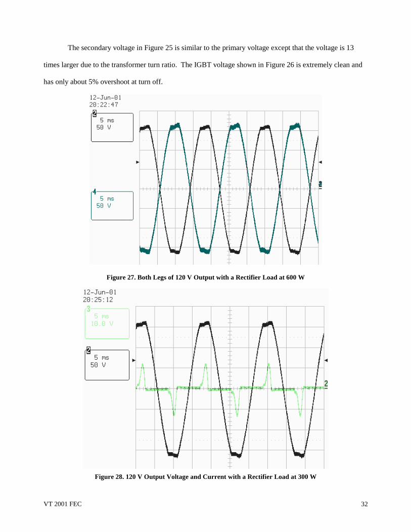
The secondary voltage in Figure 25 is similar to the primary voltage except that the voltage is 13
times larger due to the transformer turn ratio. The IGBT voltage shown in Figure 26 is extremely clean and
has only about 5% overshoot at turn off.
Figure 27. Both Legs of 120 V Output with a Rectifier Load at 600 W
Figure 28. 120 V Output Voltage and Current with a Rectifier Load at 300 W

VT 2001 FEC 33
Figure 27-Figure 29 show the waveforms with a standard full bridge rectifier load. The tops of the
waveforms are clipped, but this is to be expected. A fast Fourier transform (FFT) was performed and the
harmonics are shown in Figure 29. The fundamental is off of the screen, so the others could be determined
more accurately. The total harmonic distortion (THD) can be calculated from the FFT and is shown in (8).
The THD is only 4.36%, which is well within the specification.
%36.4%100*170
5.05.025.45.5 22222
1
2
=++++== ∑h
hTHD i
(8)
Figure 29. FFT of Rectified Load

VT 2001 FEC 34
Figure 30. Output Voltage and Current at 3.2 kW
Figure 30 shows the output waveforms for 3.2 kW as the total output power. The top two
waveforms show the output voltage and current for one leg. Channel 1 and 3 are the current waveforms, in
which 1 volt corresponds to 1 ampere of current.
Figure 31. Inductive Load Leg 1 Resistive Load Leg 2
Voltage Leg 1
Current Leg 1
Voltage Leg 2
Current Leg 2
Voltage Leg 1
Current Leg 1
Voltage Leg 2
Current Leg 2
VT 2001 FEC 35
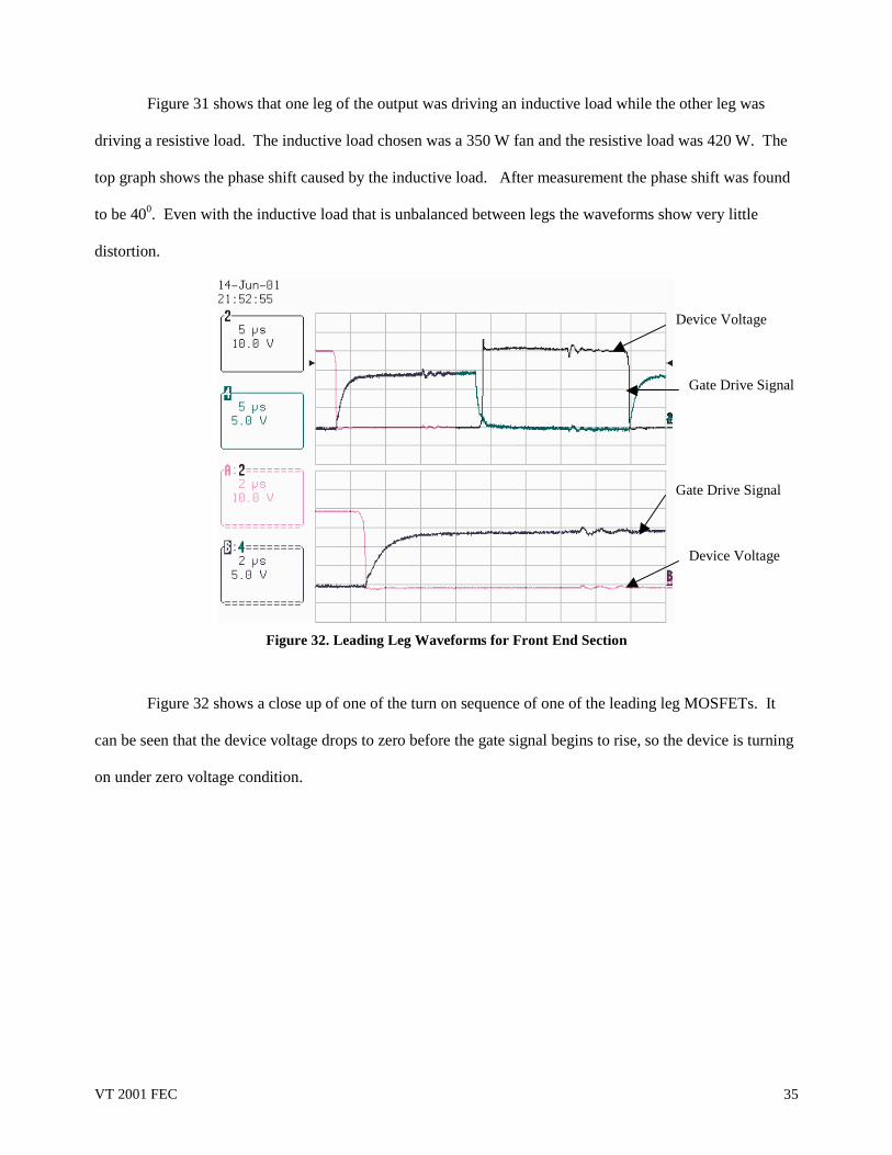
Figure 31 shows that one leg of the output was driving an inductive load while the other leg was
driving a resistive load. The inductive load chosen was a 350 W fan and the resistive load was 420 W. The
top graph shows the phase shift caused by the inductive load. After measurement the phase shift was found
to be 400. Even with the inductive load that is unbalanced between legs the waveforms show very little
distortion.
Figure 32. Leading Leg Waveforms for Front End Section
Figure 32 shows a close up of one of the turn on sequence of one of the leading leg MOSFETs. It
can be seen that the device voltage drops to zero before the gate signal begins to rise, so the device is turning
on under zero voltage condition.
Device Voltage
Gate Drive Signal
Gate Drive Signal
Device Voltage

VT 2001 FEC 36
Figure 33. Lagging Leg Waveforms for Front End Section
Figure 33 details one of the MOSFETs in the lagging leg of the front-end section of the circuit. The
device voltage begins to drop before the gate signal rises, but the voltage does not reach zero before the gate
turns on the device. This switch is in partial ZVS. The leading leg achieves ZVS at low load because the
output capacitance of the switch is discharged with the energy in the relatively large output inductance. The
lagging leg switch capacitance is discharged with the energy in the small primary leakage inductance. ZVS
will only occur in the lagging leg switches when a large current flows in the primary, storing sufficient
energy in the leakage inductance to fully discharge the output capacitance of the switches.
Gate Drive Signal Device Voltage
Device Voltage
Primary Current
Gate Drive Signal

VT 2001 FEC 37
Figure 34. Load Dump from 1.5 kW to 1.0 kW
Figure 34 and Figure 35 show the transient response of the inverter. The orange line is the power
request signal to the fuel cell and it is averaged over 10 line cycles. The response during a load dump is
virtually unnoticeable; however, the response during a large load increase shows a small oscillation in the
sine wave output. This oscillation could be corrected by tuning the control loop.
Figure 35. Load Step from 750 W to 1.5 kW
Output Power
Output Voltages
Output Power
Output Voltages

VT 2001 FEC 38
5) Comparison
The VT system has currently been tested at a 3.2 kW level. In the near future, higher power will be
attempted when a load that is capable of dissipating 10 kW becomes available. The testing was done with
unbalanced loads, rectified loads, and inductive loads in attempt to replicate a typical household load profile.
At this level the system meets all of the specifications except for efficiency, which was within 2%. The
Virginia Tech’s system exceeded all the other specifications; this performance was achieved by
implementing the latest techniques and design philosophies, which optimized the performance and reliability
of the system.
Since the final unit is to be used by the average homeowner, the Virginia Tech team wanted the unit
to be safe and easy to operate with little or no maintenance. This will make a transition from the power grid
to a fuel cell application invisible to the user. The specifications and experimental results are compared in
Table 3.
Table 3. Performance vs. Specification
Parameter Specification Experimental Output Power Capability
10 kW continuous, Single-phase 120/240 V, 60 Hz output
10 kW capability & 3.2 kW tested, Single-phase 120/240 V
60 Hz output Package Size Volume less than 50L Approximately 50L Package Weight Mass less then 32 kg ≈≈≈≈ 32 kg Overall Efficiency Higher then 90% for 10 kW resistive load ≈≈≈≈ 88% Total Harmonic Distortion
Output voltage: less than 5% when supplying a standard nonlinear load
4.36 %
Voltage Regulation Output voltage tolerance no wider than ±6% over the entire line voltage and temperature range, from no-load to full-load. Frequency 60±0.1 Hz.
Yes
Acoustic Noise No louder than conventional domestic refrigerator. Less than 50 dBA sound level measured 1.5 m from the unit.
Very little audible noise, less than 50 dBA
Protection Self-protection against output short circuit, over current, over temperature, over voltage, and under voltage or loss of input source with no damage caused by any of these.
Yes

VT 2001 FEC 39
6) Cost Evaluation
6.1) Cost Analysis Cost analysis of a design is extremely important and must always be considered if the prototype is to
have any chance of becoming a product. However, cost is also a very difficult thing to determine and
compare. Purchasing power, volume levels, and market trends are some of the factors that can affect the cost
of a design. The following table uses a relative comparison based on the component stresses to evaluate the
cost of a particular design. Keep in mind that this table is not a cost in dollars and just considers the power
capability of components.
Table 4. Relative Cost Spreadsheet
2001 FUTURE ENERGY CHALLENGE
UNIVERSITY: Virginia Tech
NAME OF MAIN CONTACT: Troy Nergaard
PROJECT NAME: FEC
DATE: 8/31/01
VOLT VOLT CUR CUR UNIT EXTENDEDDEVICE QTY DESIG UNIT MEASURE (Vpk) (Vrms) (Avg) (Arms) COST COSTDIODE 8 D1-8 600 6.03 2.39 19.11IGBT 4 IGBT1-4 400 42 6.76 27.03MOSFET 8 Q1-8 72 60 6.13 49.01CAP (ALUM) 2 Cin 6800 uF 72 4.98 9.96CAP (ALUM) 4 Cdc1-4 2200 uF 200 12.29 49.14CAP (FILM) 2 Co1-2 40 uF 200 7.98 15.96CAP (FILM) 2 Cq1-2 25 uF 72 1.23 2.45CHOKE 4 LDC1-4 300 UH 16 44.86 179.42CHOKE 2 Lo1-2 330 UH 42 73.54 147.08TRANSFORMER 2 X1 40 125 11.77 23.55CONTACTORS 1 Cont1 12 40 3.18 3.18LOSSES 900 W 75.00 75.00CONTROL 120.18PACKAGING 90.13TOTAL 811.21
The Virginia Tech team placed a lot of emphasis on cost throughout the design process. It can be
determined that the number and the size of components is directly related to cost. Therefore the goal was to
optimize the ratio between quantity and size. For instance, discrete components are priced considerable less
than modules; so discrete devices are used throughout the design. Also, the number of large passive
components is an important consideration in cost. Although four large electrolytic capacitors are used for the
DC link, it essentially allows the elimination of 8 diodes and 4 IGBTs. This tradeoff is a definite cost
reduction, not to mention a reliability improvement.

VT 2001 FEC 40
This cost optimization is difficult to do for an inverter rated at 10 kW. The Virginia Tech team
decided to go with two separate 5 kW units, which will increase the number of components by 6, yet will
decrease their size and in fact may increase reliability.
Since the spreadsheet in Table 4 does not give an absolute cost, a detailed bill of materials was
created with all of the major components used in the design. This cost estimate is based on quotes given by
common distributors of 10,000 units. Although a few prices are just estimates, Table 5 clearly shows that the
cost of the Virginia Tech design is under the $500 specification.

VT 2001 FEC 41
Table 5. Absolute Cost Spreadsheet
Component Manufacturer Part # ManufacturerPrice in 10000
Qty ($) QtyExtendedCost
($)POWER SEMICONDUCTORS
75 V, 209 A (130 A) MOSFET IRFP2907 IR 3.9 10 39.00$ 600 V, 100A (60 A) IGBT IRG4PSC71UD IR 7.8 4 31.20$
DIODES1200 V, 32 A Dual Ultrafast HFA32PA120C IR 3.5 8 28.00$
GATE DRIVES2A w/ DSAT HCPL-316J Agilent 3.32 4 13.28$ 2.5 A Charge Pump HIP4081A Intersil 3.21 2 6.42$
INDUCTORS300uH MPP Core 55104-A2 Magnetics 4.5 8 36.00$ 330 uH MPP Core 55866-A2 Magnetics 13 4 52.00$
TRANSFORMERFerrite Pot Core Custom Ceramic Magnetic 16 1 16.00$
CAPACITORS400 V, 40u Polypropolene UL30AX0400 Elcon 20 2 40.00$ 80 V, 15000u Electrolytic ECET1KA153FA Panasonic 5.45 1 5.45$ 250 V, 2200u Electrolytic ECET2EA222EA Panasonic 6 4 24.00$ 600 V, 0.15u Polypropolene 376KP/MMKP Phillips 0.43 2 0.86$ 100 V, 30u Polypropolene 3MP-16219K Elcon 4 2 8.00$
CONTROLDSP ADMC401 Analog Devices 18 1 18.00$ Phase Shift Controller UC3895 Unitrode 4.8 2 9.60$
AUX POWER SUPPLY12 V Top-Switch Circuit NA 4 1 4.00$ 15 V Top-Switch Circuit NA 4 1 4.00$ 5 V Top-Switch Circuit NA 4 1 4.00$ Isolated Gate Drive Supply NA 1 2 2.00$
SENSINGCurrent Transformer CS60-050 CoilCraft 2 2 4.00$ Linear Optocoupler HCNR201-300 Agilent 2.4 6 14.40$ Instrumentation Amplifier INA126U TI 1.1 6 6.60$ Op Amp LM833M National Semi 0.32 15 4.80$
PCB6 Layer Inverter Board Custom 4.5 1 4.50$ 4 Layer Front End Board Custom 2 2 4.00$ Control Board Custom 2 1 2.00$ 14 Layer Transformer Board Custom 15 2 30.00$
PACKAGING13" Extruded Heat Sink 420003 u2 1500 Aavid 4 3 12.00$ Case Custom 15 1 15.00$
FANS120 Vac, 9W 3906 EBM PAPST 6 3 18.00$
MISCPTC Thermistors RL5510-2560120 Keystone 1 5 5.00$ DPDT 30 A Relay T92P11D22-12 Potter & Brumfield 3 1 3.00$ 2.5 V, 4 F Ultracap PC5 Power Cache 2 4 8.00$
MANUFACTURINGLabor, Resources, ect. 8.00$
Total 481.11$
Estimated System Cost Based on Available Price Quotes

VT 2001 FEC 42
6.2) Manufacturability
There are many other factors that go into the cost of a design, including manufacturing and life-cycle
costs. The integration of the power stage with control and sensor circuits on a single PCB is a tremendous
manufacturing advantage. PCBs are relatively inexpensive to produce and can be populated almost entirely
by machines on an assembly line. Also, the planar transformer core allows a PCB to be used for the
windings, which can practically eliminate any physical labor normally involved in the construction. This
elimination of labor greatly reduces the cost and increases the reliability. The time that it takes to manually
assembly a unit will have a large impact in price because paying an employee hourly wages plus overhead
can get expensive. Thus, it is critical to make a design that can be put together with minimal manual labor.
Using a simple structure and having wiring harnesses that are pre-made and easy to connect aids this effort.
The mounting of the power devices to the heat sinks is one manufacturing challenge, but can be dealt
with if the devices are attached to the heat sinks prior to being attached to the PCBs. The final assembly
would involve connecting the front-end to the transformer via bus bars and then the transformer to the
inverter section via a single adapter board. The entire assembly would be bolted to the bottom of the case
and then the ultracapacitors and fuses could be connected to the input and output respectively. The packaged
inverter without the cover is shown in Figure 36.
Figure 36. Final Assembly

VT 2001 FEC 43
6.3) Reliability
The lifetime of the system is hard to predict accurately without years of testing. However, the
lifetime of most devices is based on thermal and electrical stress. The maximum temperature of the devices
at steady state during an average load (about 2 kW) is 40° C. During the same average load, the current
through the devices is well under rated device current. The lifetime of a capacitor is also largely dependent
on temperature; therefore, all of the capacitors used are rated at 105° C. If the ambient temperature does not
exceed 30° C, then the components should not be subjected to temperature stresses that would reduce their
lifetime. The HCPL316 gate driver will help preserve the lifetime of the system. As mentioned earlier it has
the ability to save the IGBTs even if the output is short-circuited.
The ultracapacitors are relatively new, so their standard lifetime is not well documented. However,
theoretically it has unlimited charging capability and can except large pulses of current, so the lifetime
should be much longer than the standard lead-acid battery. Some of the components that may cause the most
trouble could be the fans. To help increase the lifetime of the fans, they will be controlled with thermal
switches when the temperature gets above 50° C. This condition should only occur when the system is
operating above 3 kW. The expected lifetime of the unit should be at least 10 years with routine
maintenance and minor part replacement.
7) Conclusion
The Virginia Tech Future Energy Challenge Team has successfully designed and built a 10 kW unit
that meets or exceeds all the specifications set forth by the FEC committee. The entire design focus for the
VT Team was to build a low cost unit that exceeded all of the design specifications. This low cost approach
involved choosing a topology that minimized both part count and device ratings without sacrificing
performance or reliability. After researching many different topologies, the Team chose a 5 kW modular
design. Each module consists of a full-bridge phase shifted DC-DC converter followed by a 120 V AC half-

VT 2001 FEC 44
bridge inverter. Planar transformers are used to isolate the two stages and boost the voltage. This minimized
the part count, made 10 kW easy to achieve, and proved to meet all the specifications.
The low cost approach continued with every aspect of the system. The design philosophy of the team
was to design a system that was highly integrated. This approach lowers cost by (1) reducing manufacturing
cost, (2) part count, and (3) connections to other components. Not only does the integration decrease cost but
also greatly increases the reliability of the system. To do this printed circuit boards were designed that
incorporated both the power stage with all the sensing and driving circuits in one complete unit.
From the experimental results, it is evident that the VT Team’s design philosophy works very well.
The unit has been tested up to 3.2 kW and is projected to be less than 500 dollars in large-scale production.

VT 2001 FEC 45
8) Appendix
8.1) Calculations DCM/CCM boundary calculations based on averaged switch model of front end.
The small signal model developed by Tsai [3] for this topology was used to find the ouput powerwhere the DC/DC converter will enter CCM. The DC link filter inductor value can be adjusted to lower the power level where the converter will enter CCM. When the DCM curve in the graph crosses 1, the converter enters CCM, and the current at this duty cycle is the output current atthe boundary condition. The input and output voltages were fixed for this calculation. The filter inductor value (Lf) must be divided by two because the system has two DC links, so the there are effectively two inductors in parallel. The ripple frequency (fr) is the output ripple, which istwice the switching frequency due to the recification of the output of the converter.
fr 48kHz:= Vin 48V:=
Lk 100 10 9− H⋅:= Lf330 10 6− H⋅
2:=
n1
6.5:= Vo 200V:=
io d( )d2 Vin2⋅ Vo Vin⋅ d2⋅ n⋅−( )
2 Vo⋅ Lf⋅ fr⋅ n2⋅:= iout 4.53A:=
Pccm Vo iout⋅:= Pccm 906 W=
DCM d( ) d2 Lf⋅ io d( )⋅ fr⋅ n⋅
d Vin⋅+:=
0 0.2 0.4 0.6 0.8 10
2
4
6
8
DCM d( )
io d( )
d

VT 2001 FEC 46
FEC TRANSFORMER DESIGN
Given:
Vin 48 V. Po 10000W.
Vinmin 42 V. mod .85Vinmax 72 V.
fsmos 24 kHz Ts 1fsmos
fsigbt 24 kHz.
Cmos 2 2320. pF.
Assume:
N 213
Turns ratio = Np/Ns
η 0.90 Assuming 90% Efficiency
Vdc 400 V.
Then:
Pin Poη
Pin 1.111 104. W= Ts 4.167 10 5. s=
D
Vdc2
Vinmin 1N
. η.D 0.814= Approximate maximum rectifier
duty cycle [Note: this is twice the switch duty cycle]
Iin_ave_max PinVinmin
Iin_ave_max 264.55A=
Io Iin_ave_max N2
. Io 20.35 A=
∆ B 0.5 T. ∆ T max Ts D2
. ∆ T max 1.696 10 5. s=
VuS Vinmin∆ T max.VuS 7.123 10 4. V s.=
NA Vinmin∆ T max
∆ B.
NA 1.425 103. mm2=

VT 2001 FEC 47
Core Selection
Using E Core
60 20. 1.2 103.= Dimensions of Cross Section
E65 window area is too small
Using Planar Circular Core
Acir π 142. Acir 615.752= mm2 Need 2 turn primary
Wcir 1150 Width of Core Window
Ip 200 Is 20
k .036 .048 for outerlayer or .024 for innerlayer
t 20 Temp rise in C
oz 1.4 Thickness of 1oz copper in mils
Ap Ip
k t.44.
1.725
Ap 2.374 104.= mils^2
As Is
k t.44.
1.725
As 991.381= mils^2
Cp ApWcir oz.
Cp 14.748= Use 15 oz Copper
Cs AsWcir
7oz.
Cs 4.31= Use 5 oz Copper
10 13. 3 oz. 6. 6 oz. 8. 222.4= Board Height
Vdcmin 120 2. 2mod
. Vdcmin 399.307=
Dloss .80 Front End Duty Cycle Loss
N VinminDloss.
Vdcmin2
N 0.168 kg m2. s 3 A 1..= N = 2/13 works

VT 2001 FEC 48
8.2) Simulation Diagrams Inverter System Saber Model:
Fuel Cell and Ultracapacitor Saber Model:

VT 2001 FEC 49
Full Bridge Average Model used for Compensator Design:
vds
AC = 0TRAN =
DC = .5
0.4
C3
33.9p
-+ +
-
E2
E
vss
AC = 1TRAN =
DC =
0
Dbreak
D2
V1
5V
R2
.01
0
Rc1
9.8k
Lf
40u
1 2
Rdiv1
39k
C1
2.7n
d
Rc2
78.2k
R3
.02
Rdiv2
1k
ios
AC = 0TRAN = DC =
C2
4n
Cf
2.2m
NODESET= 200+
Rl
4
dreturn
U1
IOPAMP
01
23
PN
OUTGND
Vin42Vdc
0
0PARAMETERS:fr = 48klf = 40ulk = .1unr = 1/6.5
HB1
ZVSPWMSW
A
Dp
P
C
0
Rg
118k
0
CCMDCMtest
table((V(%IN+,%IN-)+V(D)),-1k,0,.999,0,1,1,1k,1)EVALUE
OUT+OUT-
IN+IN-
0
0
0
0
DL
Dp
+-
IA
G
0
P
0
TP
(2*I(VZC)*fr)/(V(A,P)+1u)EVALUE
OUT+OUT-
IN+IN-
VZC
0
D
-+ +
-
ECP
E
0
VDandD2
limit((V(%IN+,%IN-)+V(D)),0,1)EVALUE
OUT+OUT-
IN+IN-
Dlimit
limit(V(%IN+,%IN-),0,1)EVALUE
OUT+OUT-
IN+IN-
NUP
limit((V(D)-((V(%IN+,%IN-)+1u)*V(DL))),0,1)
EVALUE
OUT+OUT-
IN+IN-
0
0
A C
DandD2
EDL
(V(%IN+,%IN-)*lk)/nrEVALUE
OUT+OUT-
IN+IN-
CIA
v(18)*i(VZC)EVALUE
OUT+OUT-
IN+IN-
VZA
D2
(V(%IN+,%IN-)*nr*lf)/(V(D)+1u)EVALUE
OUT+OUT-
IN+IN-
CECP
V(A,P)*V(18)EVALUE
OUT+OUT-
IN+IN-
V18
V(%IN+,%IN-)/(nr*(V(DandD2)+1u))EVALUE
OUT+OUT-
IN+IN-
00
RD
1meg
18

VT 2001 FEC 50
8.3) Printed Circuit Boards The following pictures are of the PCBs that were designed by the Virginia Tech Team:

VT 2001 FEC 51
9) References [1] S. Thomas and M. Zalbowitz, “Fuel Cells-Green Power,” Los Alamos National Laboratory (LA-UR-
99-3231), 1999. [2] R. Gemmen, “Fuel Cell Dynamics and Control,” National Energy Technology Laboratory (Power
Point Presentation), January 2001. [3] F. Tsai, “Small-Signal and Transient Analysis of a Zero-Voltage-Switched, Phase-Controlled PWM
Converter Using Averaged Switch Model,” IEEE Transactions on Industry Applications, Vol. 29, No. 3, May/June 1993.
[4] S. Busquets-Monge, G. Soremekun, E. Hertz, et al., "Design of a boost power factor correction
converter using genetic algorithms," in Proc. of the Center for Power Elec. Sys. (CPES) Seminar, 2001, pp. 99-104.
[5] Franco, Sergio. Design with Operational Amplifiers and Analog Integrated Circuits. 2nd Ed. New York: McGraw-Hill, 1998.

You have reached the endof this final report.
Use the button below toreturn to the Main Document