DESIGN OF 5V DIGITAL STANDARD CELLS AND I/O...
146
DESIGN OF 5V DIGITAL STANDARD CELLS AND I/O LIBRARIES FOR MILITARY STANDARD TEMPERATURES By VIBHOR JAIN Bachelor of Engineering Electronics and Instrumentation Devi Ahilya University Madhya Pradesh, India 2006 Submitted to the Faculty of the Graduate College of the Oklahoma State University in partial fulfillment of the requirements for the Degree of MASTER OF SCIENCE July, 2008
Transcript of DESIGN OF 5V DIGITAL STANDARD CELLS AND I/O...

DESIGN OF 5V DIGITAL STANDARD CELLS
AND I/O LIBRARIES FOR MILITARY
STANDARD TEMPERATURES
By
VIBHOR JAIN
Bachelor of Engineering
Electronics and Instrumentation
Devi Ahilya University
Madhya Pradesh, India
2006
Submitted to the Faculty of the
Graduate College of the
Oklahoma State University
in partial fulfillment of
the requirements for
the Degree of
MASTER OF SCIENCE
July, 2008

DESIGN OF 5V DIGITAL STANDARD CELLS
AND I/O LIBRARIES FOR MILITARY
STANDARD TEMPERATURES
Thesis Approved:
Dr. Chris Hutchens
Thesis Advisor
_______________________________
Dr. Louis G. Johnson
_______________________________
Dr. Weili Zhang
_______________________________
Dr. A. Gordon Emslie
_______________________________
Dean of the Graduate College

iii
ACKNOWLEDGEMENTS
I would like to take this opportunity to thank my committee chair and advisor Dr. Chris
Hutchens and express my sincere gratitude for his valuable advice, patience and
understanding. I wish to express my sincere thanks to Dr. Louis Johnson and Dr. Weili
Zhang for serving on my graduate committee.
I feel proud to have served as a research assistant in the Mixed Signal VLSI Design Lab
at Oklahoma State University. It has been a wonderful and exciting learning opportunity
to work at MSVLSI Lab. I would also like to thank Dr. Chia-Ming Liu,
Mr.Vijayraghavan Madhuravasal, Dr. Hooi Miin Soo, Mr. Singaravelan Viswanathan,
Ms Usha Badam, Mr. Zhe Yuan, Mr. Srikanth Vellore, Mr. Srinivasan Venkataraman,
Ms Pratibha Kota and Mr. Rehan Ahmed and for all their help and suggestions along the
course of this work.
I am grateful to my father Mr. Keshrimal Jain, my mother Mrs. Vimla Jain and sweet
little sister Kritika Jain for their constant encouragement, love and support.
To all of them I dedicate this work.

iv
TABLE OF CONTENTS CHAPTER PAGE
CHAPTER 1 INTRODUCTION ............................................................................................................1
1.1 INTRODUCTION .............................................................................................................................1 1.2 5V DESIGN FOR MILITARY SPEC TEMPERATURES.........................................................................1 1.3 STANDARD CELL BASED ASIC DESIGN FLOW..............................................................................2 1.4 THESIS ORGANIZATION .................................................................................................................4
CHAPTER 2 SILICON ON INSULATOR WAFER TECHNOLOGY .........................................6
2.1 INTRODUCTION .............................................................................................................................6 2.2 SOI AND BULK- DEVICE STRUCTURE AND CHARACTERISTICS......................................................7
2.2.1 High Speed, Low Power and High Device Density .................................................................8 2.2.2 The Floating Body Effect [7].................................................................................................10 2.2.3 Latch-up in Bulk ....................................................................................................................11 2.2.4 SOI - Potential for lower threshold voltages (VT) .................................................................12 2.2.5 Gate Oxide Breakdown in SOI ..............................................................................................13 2.2.6 ESD Protection in SOI...........................................................................................................15
CHAPTER 3 STANDARD CELL LIBRARY CHARACTERIZATION .......................................17
3.1 INTRODUCTION ...........................................................................................................................17 3.2 DESIGN ASPECTS OF STANDARD CELL LIBRARY OPERATING AT 5V ...........................................18 3.3 STANDARD CELL LIBRARY .........................................................................................................22
3.3.1 Cell Library Design Flow......................................................................................................22 3.3.2 What's in the Box? - Components of a Cell Library ..............................................................24 3.3.3 The Layout Procedure ...........................................................................................................26
3.4 SNAPSHOTS OF CELLS..................................................................................................................28 3.5 CHARACTERIZATION OF A STANDARD CELL LIBRARY ................................................................29
3.5.1 The Library Characterizer – SignalStorm.............................................................................30 3.5.2 Gate Delay Models ................................................................................................................34 3.5.3 Characterization of Cells with Sequential Logic...................................................................37 3.5.4 Library Formats ....................................................................................................................42
3.6 ABSTRACTION OF THE STANDARD CELLS ...................................................................................43 3.6.1 Launching the Abstract Generator from layout view (Virtuoso Preview) .............................44 3.6.2 Requirements to start the Abstract Generation .....................................................................44 3.6.3 Creating Cell Abstracts .........................................................................................................46 3.6.4 Exporting LEF (Library Exchange Format)..........................................................................50 3.6.5 Optimizing the performance of Abstract Generator ..............................................................50
CHAPTER 4 CELL LIBRARY TIMING VALIDATION.................................................................52
4.1 INTRODUCTION ...........................................................................................................................52 4.2 WHY VALIDATION? ....................................................................................................................52 4.3 THE VALIDATION PROCESS.........................................................................................................53
4.3.1 Test Chip design ....................................................................................................................53 4.3.2 Test Chip Simulation .............................................................................................................56
4.4 TEST CHIP CHARACTERIZATION..................................................................................................58 4.4.1 Analysis of Delay Chains.......................................................................................................59
4.5 TEST DATA .................................................................................................................................60 4.6 DATA INTERPRETATION ..............................................................................................................64
CHAPTER 5 I/O LIBRARY – DESIGN AND CHARACTERIZATION.........................................66

v
5.1 INTRODUCTION ...........................................................................................................................66 5.2 TYPES OF I/O PADS .....................................................................................................................67 5.3 DESIGN CONSTRAINTS AND EQUATIONS:-...................................................................................69 5.4 ELECTROSTATIC DISCHARGE (ESD) PROTECTION CIRCUIT ........................................................70
5.4.1 Introduction ...........................................................................................................................70 5.4.2 What is ESD?.........................................................................................................................71 5.4.3 ESD Failures .........................................................................................................................71 5.4.4 Design of ESD Input Protection Circuit ................................................................................72 5.4.5 ESD Robustness Testing ........................................................................................................75 5.4.6 Plots and Summary of Results ...............................................................................................84 5.4.7 Conclusions on ESD robustness ............................................................................................89
5.5 CHARACTERIZATION OF I/O PADS...............................................................................................89 5.6 ABSTRACTION OF I/O PADS.........................................................................................................90
CHAPTER 6 CONCLUSION AND FUTURE WORK ......................................................................91
6.1 CONCLUSION...............................................................................................................................91 6.2 FUTURE WORK............................................................................................................................91 APPENDIX A ...............................................................................................................................................92 LIBRARY CELLS AND DRIVE STRENGTHS SPECIFICATION ..............................................................................92
Table 1: List of core cells ....................................................................................................................92 Table 2: Core cell count ......................................................................................................................96 Table 3: IO cell count ..........................................................................................................................97
APPENDIX B ...............................................................................................................................................98 INPUTS TO SIGNALSTORM LIBRARY CHARACTERIZER ....................................................................................98 APPENDIX C.............................................................................................................................................105 ABSTRACTION TUTORIAL ...................................................................................................................105

vi
LIST OF TABLES
Table 2.1 Comparison of SOI Vs Bulk .the bulk device is given a reference ‘0’, ‘+’ and
‘-’ mean “similar to bulk”, “better than bulk”, and “worse than bulk”, respectively. ...... 16
Table 3.1Cell geometry definitions and values................................................................. 25
Table 4.1 Number of load cells in the delay chains. ......................................................... 54
Table 4.2 Percent Shift in Measured data of rising delays with respect to simulated data
for FAST process at 27ºC ................................................................................................. 64
Table 4.3 Percent Shift in Measured data of Falling delays with respect to simulated data
for FAST process at 27ºC ................................................................................................. 64
Table 4.4 Percent Shift in Measured data of rising delays with respect to simulated data
for FAST process at 125ºC ............................................................................................... 65
Table 4.5 Percent Shift in Measured data of falling delays with respect to simulated data
for FAST process at 125ºC ............................................................................................... 65
Table 5.1 Measured data “Normalized” for W=10um & L=0.8um, 4 fingers.................. 74
Table 5.2 Summary of ESD testing results ...................................................................... 84

vii
LIST OF FIGURES
Figure 1.1ASIC Design Flow [4]........................................................................................ 3
Figure 2.1 Comparison between Bulk CMOS and Peregrine UTSi CMOS process [6] .... 8
Figure 2.2 Cross section of Bulk and SOI MOS devices from left to right, respectively [7]
............................................................................................................................................. 8
Figure 2.3 Layout of a CMOS inverter circuit using SOI and bulk technologies ............ 10
Figure 3.1 Plots for Ion at 27C and 125C (from left to right respectively) for NMOS
device with length of 1um, 1.3um, and 1.6um, from top to bottom respectively. [3] ...... 21
Figure 3.2 Standard Cell Library Generation Flow .......................................................... 22
Figure 3.3 The Layout format of the Standard Cell Library............................................. 24
Figure 3.4 (a) NMOS2AND (b) PMOS2AND (c) NMOS2X (d) Layout View of a
positive Edge Triggered D Flip-Flop with negative set and reset .................................... 28
Figure 3.5 Schematic and Symbol view of a positive edge triggered D Flip-Flop with
negative set and reset ........................................................................................................ 29
Figure 3.6 Inputs and Outputs to SignalStorm Library Characterizer .............................. 30
Figure 3.7 pin to pin Delays............................................................................................. 34
Figure 3.8 Delay components of a combinational logic gate............................................ 35
Figure 3.9 Measurements of propagation time and output transition time [15] ............... 36
Figure 3.10 Setup and Hold time constraints for a positive edge triggered flip-flop ....... 38
Figure 3.11 Setup time measurements using binary search [15] ...................................... 40
Figure 3.12 Basic Abstract generator flow ....................................................................... 43
Figure 3.13 Types of Layout and Logical data that can be imported into the abstract
generator and the format of data that can be exported...................................................... 46
Figure 3.14 Cell Pane showing various warning signs and progress in Abstraction Steps
........................................................................................................................................... 49
Figure 3.15 Abstract view of Tristate buffer with 8X drive strength and inverted output 50
Figure 4.1 Design of NAND Delay Chains ...................................................................... 54
Figure 4.2 Load cell - NAND, NOR or Inverter followed by inverter ............................. 55
Figure 4.3 Layout of the delay chain circuits ................................................................... 56
Figure 4.4 Simulation Set up for the Delay Chains .......................................................... 57
Figure 4.5 Schematic of the Pad Frame ............................................................................ 57
Figure 4.6 Inverter timing waveforms recorded on Oscilloscope showing the input
padded out and pulses showing rising and falling delay of the input waveform.............. 58
Figure 4.7 Rise and fall delay plots (left and right, respectively) for Inverter followed by
Inverter module at 27C and 125C (upper two plots and lower two plots, respectively). . 61
Figure 4.8 Rise and fall delay plots(left and right ,respectively) for Nand followed by
Inverter module at 27C and 125C (upper two plots and lower two plots, respectively). . 62
Figure 4.9 Rise and fall delay plots (left and right, respectively) for Inverter followed by
Inverter module at 27C and 125C (upper two plots and lower two plots, respectively). . 63
Figure 5.1 Snapshot of Layout of a Bidirectional pad, with an Active pull-up transistor of
20kOhms........................................................................................................................... 68
Figure 5.2 Snapshot of Schematic of a Bidirectional pad, with an Active pull-up transistor
of 20kOhms....................................................................................................................... 69

viii
Figure 5.3Drain-junction damage in an NMOS after HBM stress. Figure 5.4 Gate-oxide
damage to an input buffer after Note the thermal damage to silicon.
CDM stress. Note the rupture in gate oxide. [17] ............................................................. 72
Figure 5.5 Conceptual ESD protection circuit for an Input pad ....................................... 73
Figure 5.6 Input pad test structure with drive strength of 1X and input capacitance of13fF
........................................................................................................................................... 75
Figure 5.7 ESD Test modes .............................................................................................. 76
Figure 5.8 Human Body cause a electric discharge on a device under test (DUT) .......... 81
Figure 5.9 The Human Body Model set up circuit ........................................................... 81
Figure 5.10 Set up for Pre and post Exposure gate leakage and VTC measurements ...... 82
Figure 5.11 Flowchart describing the ESD test procedure for Human Body Model........ 83
Figure 5.12 Post ESD exposure test results for test structures with clamp NMOS
transistor of length 1.4um at 125C and 27C ..................................................................... 86
Figure 5.13 Post ESD exposure test results for test structures with clamp NMOS
transistor of length 1.5um at 125C and 27C ..................................................................... 87
Figure 5.14 Post ESD exposure test results for test structures with clamp NMOS
transistor of length 1.6 um at 125C and 27C .................................................................... 88

CHAPTER 1 INTRODUCTION
1.1 Introduction
Application Specific Integrated Circuits are used to design entire systems on a single
chip. ASICs are interconnection of standard cells which have been standardized by
fabrication houses. With the integration of more and more system components on a single
IC, the complexity of IC fabrication has increased. Modern day system design involves
complex layout issues. Specifications of cells are provided by the vendors in form of a
technology library which contains information about geometry, delay and power
characteristics of cells. Design flow of ASICs is highly automated. The automation tools
such as library characterizer, Abstract view generators, Automatic Place and Route tools
etc., provide excellent performance and cost advantages over manual design process.
1.2 5V Design for Military Spec Temperatures
As the operating temperature increases, bulk Silicon devices fail to operate due to
substrate diode leakage currents. Silicon on Insulator (SOI) is found to overcome most of
the problems of bulk silicon at temperatures of military spec and above [2] including
radiation tolerance. The operating voltage of the designs was chosen to be 5V based on
proper device behavior with this operating voltage and temperatures as high as 125°C.
This was followed by selecting the device geometries to minimize the leakage, punch
through, and avalanche at 5V operation and 125°C.

2
1.3 Standard Cell Based ASIC Design Flow
As designs grow in complexity day by day, it is becoming increasingly difficult to layout
these circuits by hand. Hence a custom ASIC (Application Specific Integrated Circuit)
cell library approach is desirable. Standard cell based design provides reusability of basic
cells for various designs and gives optimal level of abstraction. The cell based ASIC
design flow diagram shown in Figure 1.1 categorizes the entire design procedure into
tasks that fall under several design teams. The design procedure for ASICs given a fully
characterized standard cell library is as follows [3]:
1. A synthesizable behavioral description of design in high-level description language
(VHDL or Verilog) is written. This is called RTL (register transfer level) design.
2. The suitable functionality of the RTL code is verified by simulation.
3. Design partitioning into fewer smaller blocks is performed. This provides easy
handling of design, efficient synthesis results with reduced time to market and reusability
and fewer errors.
4. Logic synthesis on the RTL description is performed. This maps design on to standard
cells and connectivity between them. This provides a gate-level net list depicting standard
cells and electrical connections between them.
5. Functional simulation and static timing analysis are performed on the synthesized
code.
6. A gate-level net list is imported into a place & route tool. Floor planning, power
planning, placement, In Place Optimization (IPO) and trial route are performed on RTL
level netlist imported. Clock tree synthesis and timing analysis are performed. All the

3
partitioned blocks are brought together at place & route level either with individual
blocks placed & routed to give a block.
Figure 1.1ASIC Design Flow [4]

4
7. Post layout simulation is performed and static timing is back annotated. Testing is
performed demonstrating the functional correctness of the design over all extremes of
process, voltage and temperature.
8. Physical verification (DRC and LVS) is performed at the end before the design is sent
to semiconductor facility for fabrication. As designs grow in complexity day by day, it is
becoming increasingly difficult to layout these circuits by hand. Hence a custom ASIC
(Application Specific Integrated Circuit) cell library approach is desirable. This approach
enables the designer to convert a design from its functional description in high level RTL
(Register Transfer Level) code such as Verilog or VHDL to layout with minimum effort
using automatic Placement & Routing (PNR) tools. The cell library would contain a set
of combinatorial and sequential logic cells of different drive strengths with their
corresponding layout, schematic and symbol views and their characterized timing and
power models.
1.4 Thesis Organization
This thesis consists of 6 chapters. Chapter 2 describes the details of Silicon on Insulator
(SOI) implementation and its advantages over a typical bulk CMOS process. Chapter 3
describes the details of the cell library, its format, and library design guidelines,
characterization of cells for timing and Abstraction of cells. Chapter 4 deals with
Validation of the cell library. Chapter 5 deals with the I/O Pads Design and
Characterization followed by the significance of Electro Static Discharge (ESD)
protection circuits and its design. This is further followed by the testing scheme of

5
Human Body Model (HBM) at room temperature and military spec temperature at 125C
followed by the ESD measurement results. Chapter 6 discusses future work in the
direction of I/O pad design and ESD structures.

6
CHAPTER 2 SILICON ON INSULATOR WAFER
TECHNOLOGY
2.1 Introduction
Silicon-On-Insulator (SOI) is a semiconductor fabrication technique that uses pure crystal
silicon and silicon oxide for integrated circuits (ICs) and microchips. An SOI microchip
processing speed is often 30% faster than today's complementary metal-oxide
semiconductor (CMOS)-based bulk chips of equal dimension and power consumption is
reduced 80%, which makes them ideal for mobile devices. SOI chips also reduce the soft
error rate, data corruption resulting from cosmic rays and natural radioactive background
signals striking the IC. The SOI performance advantage over bulk is caused by the
elimination of the junction capacitance, and the lack of reverse body effect in stacked
circuits and the fact that the SOI body is slightly forward biased under most operating
conditions [5]. At elevated temperatures such as 100 C – 300 C, the bulk devices fail to
operate in contrast to SOI devices, typically owing to its device leakage characteristics.

7
2.2 SOI and Bulk- Device Structure and Characteristics
In bulk processes, individual devices are fabricated in the body of silicon and large area p
n junctions are used for isolating drain and source of P/N type MOS transistors from the
substrate. In an n-well process, N type MOSFETs are fabricated in p type silicon
substrate and P type MOSFETs are fabricated in an n-well diffused in p type silicon
substrate. Drain and source of NMOS transistors are isolated from substrate by p-n
junction formed by drain or source itself with silicon substrate. Drain and source of
PMOS transistors isolated from silicon substrate using an n-well. On the other hand,
devices in SOI process are fabricated in silicon thin film active layer over a buried oxide
layer (BOX). The BOX layer being an insulator providing isolation of transistors from
silicon substrate underneath it and local oxidation of silicon (LOCOS) or removing of
unused silicon between transistors isolating individual transistors. In fully depleted SOI
process, thickness of silicon film over insulator is less than approximately 50nm.Thus the
entire silicon film is taken by source/drain depletion region leaving no body. Whereas in
partially depleted SOI process, silicon film thickness is around 100nm to 200nm or
thicker giving rise to the existence of a body that is floating.

8
Figure 2.1 Comparison between Bulk CMOS and Peregrine UTSi CMOS process [6]
2.2.1 High Speed, Low Power and High Device Density
N
plusN
plus
CSB CDB
P-substrate
N
plus
N
plus
silicon
substrate
Oxide
P
Figure 2.2 Cross section of Bulk and SOI MOS devices from left to right, respectively [7]
SOI can reduce the capacitance at the source and drain junctions significantly by
eliminating the depletion regions extending into the substrate, as shown in Figure 2.2.
This is responsible for reduction in the RC delay due to parasitic capacitance which

9
accounts for higher speed performance of the SOI CMOS devices compared to bulk
CMOS, particularly at the downscale power supply voltage.
Owing to the buried oxide structure, the source/drain regions of the SOI NMOS/PMOS
devices can be placed in closer proximity each other without the possibility of latch up.
Therefore, SOI CMOS devices typically have a much higher device density. Figure 2.3
shows the layout of a CMOS inverter circuit using SOI and bulk technologies [8]. As
shown in Figure 2.3, since wells are not required to separate the N+ region from the P+
region, the smaller layout area of the SOI CMOS circuits leads to smaller leakage current
and smaller parasitic capacitances. Since SOI devices do not need the reverse biased
junctions and well isolations, their device density can be even higher. As a result, a
higher speed at smaller power consumption can be obtained from the SOI CMOS circuits
for device of equal channel lengths. Consequently, SOI CMOS devices are appropriate to
integrate low-power circuits.

10
Figure 2.3 Layout of a CMOS inverter circuit using SOI and bulk technologies
2.2.2 The Floating Body Effect [7]
Despite supporting higher speeds, low power and high device density in circuit design,
SOI technology possesses certain structural issues. The MOS device is always
accompanied by a parasitic transistor connected in parallel. Unlike the case in bulk
silicon, the base of the bipolar transistor is not connected to ground and is floating. When

11
the MOS transistor is biased in the saturation region and the drain voltage exceeds a
certain value, the bipolar transistor turns on where the drain current suddenly rises with a
discontinuity in the drain current on the I-V curves [9], this is referred to as the kink
effect. Kink effects are unique in the partial depletion (PD) SOI devices, which means
when the body of the device is not depleted fully. In Fully Depleted (FD) devices, the
silicon film is fully depleted at threshold and due to the full depletion of the film the
source to body potential barrier is very small. As a result, on applying drain voltage high
enough to create electron hole pairs the holes readily moves to the source without raising
the body potential. Hence, the body potential doesn’t change and thus FD devices are
virtually free of the Kink effect.
In order to reduce the kink effect, one method is to provide a body contact for the device
to the supply rail, but this greatly increases the area of the circuit and degrades the feature
advantage of high device density and small parasitic capacitance.
2.2.3 Latch-up in Bulk
In bulk silicon, the formation of a thyristor like PNPN structure with a parasitic PNP and
NPN transistor connected back to back results in latch-up. Latch-up is the creation of a
low impedance path between the power and ground rails by triggering the thyristor
structure. Once triggered both transistors start conducting and large amounts of current
start flowing through the devices until the power is switched off. Latch-up degrades
circuit performance typically resulting in destruction of the device due to over currents.
In SOI, there is no direct path between the various devices and the devices are isolated by

12
a layer of thick oxide which surrounds each device [10]. Hence latch-up can never occur
in SOI.
Figure 2.5 Cross-sectional view of an inverter showing parasitic bipolar transistors
connected back to back [11]
2.2.4 SOI - Potential for lower threshold voltages (VT)
The inverse subthreshold slope which is defined as the inverse of the slope of ID (VG)
curve in subthreshold regime is given by equation 2.1
),1)(10ln()/(
)(log/
α+=
=
qkT
IddVS DG
(2.1)
Here α represents the ratio of the capacitance between inversion channel and the back
gate electrode, and the gate oxide capacitance. Typically, α fully depleted SOI < α bulk
As a result, inverse subthreshold slope has the lowest (i.e. better) value in the fully
depleted device than in bulk device. Typically, the value obtainable for fully depleted
SOI is 65mV/ decade [18] in comparison to 90mV/ decade [12] for bulk process. The
lower values of inverse subthreshold slope in fully depleted SOI devices allows one to
use smaller values of threshold voltage than in bulk devices without increasing the

13
leakage current at Vg = 0. As a result, better speed performances can be obtained,
especially at low supply voltages.
2.2.5 Gate Oxide Breakdown in SOI
At high supply voltages both leakage currents and avalanche currents can be increased
leading to circuit malfunction. As a result considerations must be under taken to avoid,
avalanche breakdown, gate oxide break down and excessive leakage current as a result of
the bipolar kink effect. Due to reduced gate oxide thickness, a high voltage applied across
gate and substrate results in high electric fields across the oxide. When the oxide is
subjected to high electric fields, electrons will tunnel through oxide layer and contribute
to gate current. With increase an in electric field across the oxide, for values greater than
a certain threshold, oxide starts breaking down completely giving rise to very large gate
currents thereby causing the device to fail. Gate tunneling was not found troublesome
when the NMOS and PMOS devices were tested for Peregrine process (A Fully Depleted
Silicon on Sapphire process). It can be seen in Figures 2.6 and 2.7 that the devices show
no signs of gate tunneling when powered up to 8V[3].

14
Figure 2.6 Gate Break down Voltage of Regular PMOS @ 275 C [3]
Figure 2.7 Gate Break down Voltage of Regular NMOS @ 275 C [3]

15
2.2.6 ESD Protection in SOI
While electrostatic discharge protection devices have been implemented as ancillary
circuits on MOS type integrated circuit chips, an additional concern arises with SOI
chips. Traditionally, the energy of an electrostatic discharge was maintained at a safe
voltage level by such ancillary protection circuits, and the energy was dissipated in the
bulk semiconductor substrate on which the circuits were fabricated. In contrast, for SOI
circuits, the thin silicon layer is electrically and thermally insulated from the substrate by
a buried oxide (BOX) layer. Since most electrically insulating materials are poor thermal
conductors, substantially all the energy must be dissipated within the thin polysilicon
layer which overlies the insulator (buried oxide). A floating body field effect transistor
having a defined breakdown voltage, and a lower holding voltage, serves to clamp
electrostatic discharge voltages to a low voltage level, thereby minimizing thermal power
dissipation within the thin semiconductor layer of SOI circuits. NMOS devices have
been used predominantly for ESD protection circuits over PMOS devices owing to lower
snapback voltages of NMOS devices [16].

16
In summary, a comparison of SOI Vs Bulk can be tabulated as shown in table 2.1
BULK SOI
Source & Drain Cap/ Speed 0 +
Device Density 0 +
Inverse Sub-threshold Slope 0 0/+ (partially depleted/
fully depleted)
Latchup 0 +
Kink 0 -
Conventional
ESD protection methods
0 -
Table 2.1 Comparison of SOI Vs Bulk .the bulk device is given a reference ‘0’, ‘+’ and
‘-’ mean “similar to bulk”, “better than bulk”, and “worse than bulk”, respectively.

17
CHAPTER 3 STANDARD CELL LIBRARY
CHARACTERIZATION
3.1 Introduction
The requirement of a Standard Cell Library (SCL) in the ASIC Design world is
unavoidable. A standard cell library is comprised of combinatorial and sequential logic
cells of different drive strengths with their corresponding layout, schematic and symbol
views and their characterized timing and power models. A SCL enables a designer to
easily translate a design from its high level description in Verilog or VHDL to a layout
using placement and routing tools. At the early design stage, cells are targeted to meet
certain function and performance requirements. Typically, the cells can be designed with
the intent to either optimizing for area or in optimizing speed. The former typically uses
minimum sized transistors to achieve the smallest area while the latter uses larger
transistors to provide good drive qualities since the “on” resistance of the transistors is
inversely proportional to the width of the transistor. An optimum scaling ratio (3 in case
of our buffers) of the driven and the driving transistors allow for higher drive currents
along with tolerable input capacitance for the drive transistor. As a result it takes less
time to charge a lower capacitance and hence increment in speed is achieved.

18
3.2 Design Aspects of Standard Cell Library operating at 5V
There are certain factors that need to be considered when designing a standard cell library
for 5V and military spec temperature applications. The factors that need to be considered
are:
1. Selection of proper lengths for transistors to meet leakage current, bandwidth and
noise margin requirements at temperatures such as 125C. Operating conditions for
the intended use of the cell library and its performance requirements dictate
geometries for NMOS and PMOS devices to be used in the library. The cell
library project was designed to operate at 5V and up to temperatures of 125°C.
The Peregrine processes are designed to be a 4V process. At high supply voltages
both leakage currents and avalanche currents can be large leading to circuit
malfunction. As a result considerations must be under taken to avoid, avalanche
breakdown, gate oxide break down and excessive leakage current as a result of the
bipolar kink effect. Avalanche breakdown is a current multiplication process that
occurs in the presence of strong electric fields caused by even moderate voltages
over very short distances like in semiconductor devices. The voltage at which
avalanche breakdown occurs in a given device poses an upper limit on the
operating voltages because; the associated electric fields can start the process and
cause excessive current flow resulting in destruction or rapid aging of the device.
Several NMOS devices with gate lengths starting 1µm and PMOS devices with
gate lengths starting from 0.5µm have been tested on silicon at room temperature
and 125°C with drain voltage of 5V [3]. The data shows that the electric field to
which the carriers are subjected to, by applying up to 5V across drain and source

19
does not start the avalanche breakdown process for NMOS devices with channel
lengths in excess of 1.6um and for PMOS devices with lengths greater than
0.8um. Thus avalanche is not a problem even for minimum length PMOS devices
for a 5.5V of power supply both at room and 125°C [3] while 1.6um devices were
used for the NMOS devices.
2. Of several process-level and circuit-level techniques available for reducing
leakage currents, controlling lengths of the devices is used for this work. Since
NMOS devices were found to avalanche and leak more than the PMOS at shorter
channel lengths, design starts by choosing channel length for NMOS device that
would give an acceptable Ion/Ioff ratio and control avalanche. Hardware testing
was performed on several NMOS devices with different lengths at room
temperature and 125°C to obtain Ion/Ioff ratios. Plots for on-state current and off-
state current are shown in figure 3.1. A channel length of 1.6µm was selected for
the NMOS device that is tested to demonstrate Ion/Ioff ratio of more than 80 at
125°C as is evident from plots shown in figure 3.1 for NMOS device with gate
length of 1.6µm. Channel length of 0.8µm is chosen for PMOS device while both
devices were designed with equal device widths of 1.4um. This resulted in the
logic devices being approximately beta matched the transistors.[3]
3. Gates were beta matched to maximize the noise margins over optimal delay or
minimum geometry given the application environment.
4. Avoiding or minimizing usage of transmission gates to eliminate potential
floating body problems in SOS.

20
5. Limiting the number of series connected transistors to four or less. When the
number of series connected transistors is large, the rise/fall times degrade due to
higher resistance and greater self capacitance.

21
Figure 3.1 Plots for Ion at 27C and 125C (from left to right respectively) for NMOS
device with length of 1um, 1.3um, and 1.6um, from top to bottom respectively. [3]

22
3.3 Standard Cell Library
3.3.1 Cell Library Design Flow
The standard cell library design process broadly involves three stages which are
illustrated in Figure 3.1 and explained in detail below [13].
Figure 3.2 Standard Cell Library Generation Flow
1. Standard Cell Generation – As the name suggests, standard cells perform certain
combinatorial and/or sequential logic function such as NAND, NOR, Latch etc, which
are considered as standards in ASIC design industry. This involves selection of the
correct device (transistors) geometries, creating schematics and symbol views (Logical
view), drawing layouts (Physical view) according to specifications followed by Design
rule Check (DRC) and Layout Versus Schematic (LVS) checks, further followed by
extraction of the SPICE netlist for each cell.
Design
Layout
Characterization Physical Abstraction
1. Standard Cell
Generation
2. Timing and
Power
3. Physical
Description of Cells

23
2. Generating Timing and Power Data – The timing values which are categorized as
intrinsic rise/fall time, rise resistance, fall resistance, setup and hold time (for sequential
cells) for the cells, are characterized using SignalStorm (a Cadence Design Suite tool).
Power consumption refers to three types of power:
• Switching power, this is due to the charging and discharging of the loading
capacitance.
• Short-circuit power, this is due to the current drawn from supply to ground when
the output switches. Short-circuit power depends on both the input slew rate and
the output loading capacitance.
• Static leakage power, which is due to the static current drawn from supply to
ground when the circuit is stable.
SignalStorm library characterizer characterizes all three types of power consumption and
saves the results in tabular format in the database. The timing and power information is
put together to form a “.lib” file (Synopsis Liberty File, this format is an industry
standard) which can be used by the synthesis tool to convert the behavioral code to a
Verilog netlist that meets the timing constraints.
3. Physical Description of Cells – This step involves creating the abstract view of each
cell which is basically a physical description of the cell having the information about the
different layers of metals used in the layout, the different metal layers available and the
preferences of these layers for routing, the area of each cell along with the dimension of
the power and ground rails and the pin positions so that the router can route the I/O pins.

24
3.3.2 What's in the Box? - Components of a Cell Library
Irrespective of the vendor, the standard cell library must have:-
1. Circuit Schematics, Symbols, Layouts, Parasitic Extraction and Abstracted views
of each standard cell.
2. Technology Libraries giving the Timing and Power specifications for the Worst,
Normal and Best case in terms of threshold voltage, temperature, Process and
operating voltage in a format that is accurate and acceptable industry wide for
synthesis and Place & Route (P&R).
3. A routing model for proper routing of the design in order to avoid design rule
errors.
4. A behavioral model which describes the functionality of each cell.
5. A model in Verilog /VHDL for all the cells.
6. Cell Library Documentation highlighting the relevant information and guiding the
user through the timing and power data.
Figure 3.3 The Layout format of the Standard Cell Library

25
Table 3.1Cell geometry definitions and values
Parameter Value for a single
height cell
Comment
gx 2.2um Horizontal grid spacing. (isolated metal width)
gy 2.2um Vertical grid spacing.
Sy , Sx 0.9um (NMOS rail)
0.4um (PMOS rail)
0.4um
Safety zone required to avoid abutting DRC errors.
Safety Zone to avoid abutting errors from left and right
side of the cell
wp 2.4um Power rail width
h 24.2 um
(m*gy)
m vertical grids equals 11
wuse (n-1)gx n horizontal grid points must be an integer

26
3.3.3 The Layout Procedure
This section illustrates how the cells were created using manual layout techniques in
cadence virtuoso layout editor. Layout uses standard cell techniques where signals are
routed in polysilicon, nominally perpendicular to the power rails. Layout format followed
in developing the standard cell library is shown in figure 3.2 with geometry definitions
and values summarized in Table 3.1. This approach results in a dense layout for CMOS
gates. Once lengths and widths of transistors are finalized, the following steps are
followed:-
1. Cell height is chosen to be the lowest possible integer multiple of metal1 routing
grid that could accommodate the most complex cell in the library such as a flip-
flop or a full adder. In this way it is ensured that any other cell in the entire library
would fit in that fixed cell height. The finalized height was 24.2um.
2. All the pins of each should be placed on grid points (multiples of 2.2 um in our
case), thus avoiding slow off-grid routing.
3. Pins are staggered wherever possible allowing for easier pin access by the routing
tool.
4. Contacts are merged for improved density but kept at greater than two to provide
greater reliability.
5. Verification is performed to make sure that each cell passes DRC and LVS
checks.
6. Care has to be taken to keep apposition error in mind, i.e. when two NMOS
device in the cells are placed side by side and apposition abutting errors can
result. Hence there has to be some spacing (generally half the spacing required to
avoid any DRC error) left for each layer in the layout at each cell’s boundary area.

27
The power rails are 2.4um wide, routed horizontally in metal1. The I/O of the cell is
routed vertically in metal2 over the cell, connecting to terminal pins defined by labeled
metal2-metal1 pins. As the routing of the I/O is over the cell, the I/O terminals can be
placed anywhere on the predefined grid points. All I/O pins are placed on a ‘gx’ by ‘gy’
grid to get increased efficiency with place and route tool. All cells are ‘n’ times ‘gx’ wide
where ‘n’ is the lowest possible integer that accommodates the cell. Also since routing
tools use fixed-grid three-level routing, the terminals must have a center-to-center
spacing along both axes. All metal1 must be wholly contained between the power rails;
only polysilicon and locos are allowed to extend to within ‘ss’ of the cell boundary.
Metalthick when used runs horizontally while metal2 runs vertically. The grid spacing gx
and ‘gy’ are set respectively by the minimum spacing requirement between two m1-m2
vias and m2-mt vias. The routing grid is chosen to be 2.2um for metal1 and metal2.
A practice of creating instances of small cells has been followed throughout the cell
library. These cells include NMOS and PMOS with 1X, 2X, 4X drive strengths and P/N
ratio is set so as to have the transistors beta matched. There are cells with NAND
Function of strengths 0.5 X, 1X, 2X and3X. Such usage reduces the manual design time
to a great extent at a minor or no expense in area.

28
3.4 Snapshots of cells
(a)
(b) (c)
(d)
Figure 3.4 (a) NMOS2AND (b) PMOS2AND (c) NMOS2X (d) Layout View of a
positive Edge Triggered D Flip-Flop with negative set and reset
PMOS2AND Merged Contacts ensure
greater reliability
NMOS2X NMOS2AND
Pins on grid (2.2um)

29
Figure 3.5 Schematic and Symbol view of a positive edge triggered D Flip-Flop with
negative set and reset
3.5 Characterization of a Standard Cell Library
Characterization is the process of exhaustively analyzing an entity at a low level of
abstraction to extract all relevant and meaningful information about it, and then to
faithfully represent that information in a model at a higher level of abstraction. Cell
characterization is the foundation on which the entire high-level RTL-to-GDSII flow has
been built. Without accurately modeled ASIC cells IC design would take longer, require
more people and software licenses, and suffer even more problems with failing
prototypes than it does today. High quality, accurate and robust ASIC cell libraries enable
implementation and verification flows for ASIC designers. A cell library needs to be
characterized for timing and power to generate a detailed timing model file for use by the
30
synthesizer to optimize the design and to verify that the timing constraints are met. Once
a design has been completed through P&R, the next step is to understand the inherent
delays associated with the completed routing.
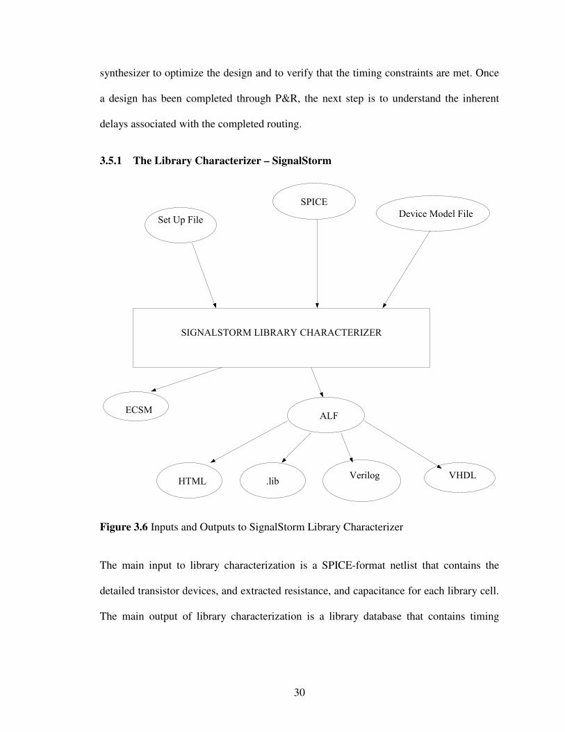
3.5.1 The Library Characterizer – SignalStorm
SIGNALSTORM LIBRARY CHARACTERIZER
Set Up File
SPICE
Device Model File
ECSMALF
HTML .libVerilog VHDL
Figure 3.6 Inputs and Outputs to SignalStorm Library Characterizer
The main input to library characterization is a SPICE-format netlist that contains the
detailed transistor devices, and extracted resistance, and capacitance for each library cell.
The main output of library characterization is a library database that contains timing

31
models for each of the cells. These timing models are used in delay calculation.(see
Figure 3.6). Sample input and output files used in SignalStorm are shown in Appendix B
SignalStorm performs the following steps for automatic cell library characterization [14]:
1. Analysis of Spice models of transistor circuits and recognition of the logic
structure and functionality.
2. Generation of the logic model or function model for combinatorial, sequential and
tristate circuits.
3. Generation of specification definitions in the circuit such as pin directions and
properties, pin to pin delays etc.
4. Generation of Delay Vectors.
5. Generation of Power Vectors.
6. Defining the cell library characterization environment by specifying parameters
such as the supply voltage, temperature, input slew rate, output load and process
corners (Fast ,Typical and Slow)
7. Execution of Spice netlist and summarizes the results.
8. Generation of Abstract Library Format (ALF) file which can be further converted
to .LIB, .VHDL, .V and HTML files.
A standard cell is usually characterized in terms of input slew rate “tin” and output load
capacitance “CL” for different supply voltages, temperatures and process corners such as
slow, typical and fast corners. The standard cells are characterized for output transition
time, propagation delay from each input pin to the outputs, internal switching power,

32
leakage power dissipation and input pin capacitances. In addition to these, sequential
cells are characterized for setup time and hold time.
The various factors that are taken into account to characterize a cell for its Timing are:-
• Intrinsic Delay – It is an important benchmark of transistor performance. Given
by τ= CV/I, where C is the gate capacitance, V = Vdd, and I is ON current Ion.
As defined, τ represents the fundamental RC (where R is the device “on”
resistance and C is the capacitance) delay of the device and provides a frequency
limit for transistor operation that is relatively insensitive to gate dielectrics and
device width. It is the delay of a logic gate driving its own gate (transistor gate).
This parameter is estimated by the user and is to be taken care of while setting the
values of different parameters in the set up file for characterization. Running the
tools for slew times faster than intrinsic delay or 1/ωT is merely wasting the run
time of the tool as the gate can not respond to slew times faster than intrinsic
delay.
• Input Slew –The delay of a gate is determined by the rate at which the input is
rising / falling and also on the output loading capacitance that gate is driving. The
lower limit of the slew time is fixed by the intrinsic delay or 1/ωT of the simplest
gate (inverter) and the maximum limit is determined by the maximum allowable
output slew for the library selected by the designer. As a general rule the selected
maximum input slew rate for characterization should not be faster than 2/ωT.
• Output Loading Capacitance LC -The pin capacitance seen by the cell
determines the output slew. The load capacitance should be selected as
normalized load for each gate drive strength from 1X to 8X or 16X, i.e. 1X, 2X,

33
3X, 4X, 8X. The exception is when determining intrinsic delay in which case the
normalized load must be small i.e X/20.
Since the amount of delay and rise/fall times depends upon both the input slew rate
and the output pin capacitance (loading), library characterization executes simulations
by using different input slew rates and output loading capacitance combinations.
• The input slew rate, output loading and calculated pin to pin delay (see Figure
3.7 [14]) is saved as a two dimensional delay table.
• The output slew rate which is also calculated by these SignalStorm SPICE
simulations, is saved in a second table.
Using the characterization data contained in these two tables, the SignalStorm library
characterizer provides the delay/ driver model for specific pin –to pin delays. Pin-to-pin
delay is the time that it takes a change at an input pin to effect a change at an output pin.
The time is measured from the point when an input signal switches through an input
threshold voltage (Vthi) to the point when an output signal switches through an output
threshold voltage (Vtho), as shown in Figure 3.7 and explained in detail the section 3.5.2.

34
Unloaded
or intrinsic
delay
INPUT
OUTPUT
Vthl
VthO
Loaded
delay
Loaded
delay
OUTPUT
VthO
Unloaded
or intrinsic
delay
Figure 3.7 pin to pin Delays
3.5.2 Gate Delay Models
The accuracy of the synthesized circuit depends upon the level of details and accuracy
with which the individual cells have been characterized. There are a number of delay
models with a trade off between accuracy and performance. In general, the delay of a
standard cell is a function of the fan-out and the rise and fall times of the input signals.
One of the popular delay models is illustrated in Figure 3.8 and is briefly described here.
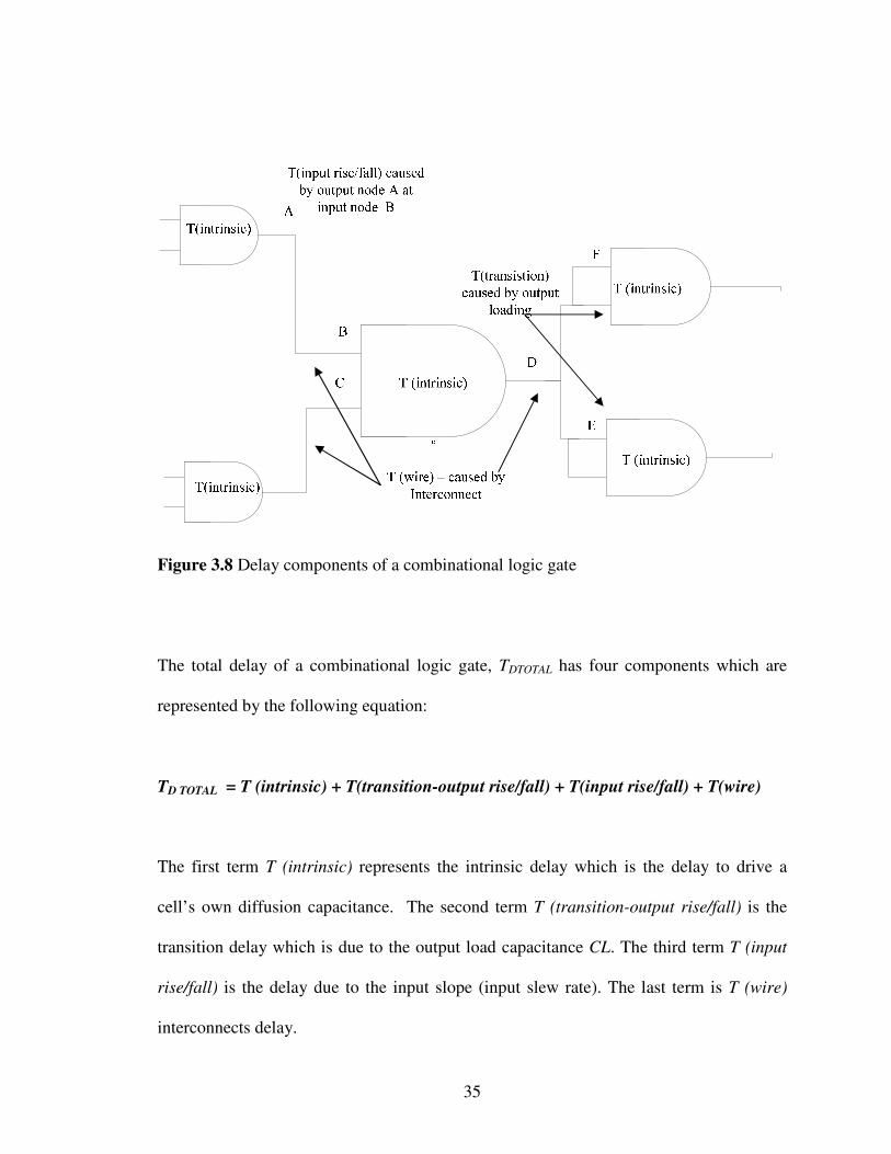
35
Figure 3.8 Delay components of a combinational logic gate
The total delay of a combinational logic gate, TDTOTAL has four components which are
represented by the following equation:
TD TOTAL = T (intrinsic) + T(transition-output rise/fall) + T(input rise/fall) + T(wire)
The first term T (intrinsic) represents the intrinsic delay which is the delay to drive a
cell’s own diffusion capacitance. The second term T (transition-output rise/fall) is the
transition delay which is due to the output load capacitance CL. The third term T (input
rise/fall) is the delay due to the input slope (input slew rate). The last term is T (wire)
interconnects delay.

36
Each standard cell is characterized to determine the propagation delay from each input
pin to the output pin and the output transition time. These values are usually measured
between pre-determined threshold values of the signal edges (10% - 90% in our case).
The methodology of measuring these two delay values is illustrated in Figure 3.8. In
simple terms gate transition time consist of intrinsic delays and transition delays were
transition delay are effected by the input transition and loading of the gate and by the
wire delay.
Figure 3.9 Measurements of propagation time and output transition time [15]
The propagation time is often measured from 50% of the input voltage to 50% of output
voltage signal. The output transition time is measured from either 10 – 90 % or 20 – 80%
to have the simulation with realistic values. The values of output transition time and
propagation time are required for gate level synthesis and delay calculation tools. In
synthesis, the output transition time is used for estimating the input slew rates of
successive cells and the propagation time of each cell is extracted from the delay table
based on the input slew rate and output load (see Appendix B- ALF and LIB formats).

37
Hence, the delay between two nodes in a design can be calculated with the propagation
time and output transition time of each cell on the path between two nodes.
3.5.3 Characterization of Cells with Sequential Logic
Input Constraints of Sequential Logic : For sequential logic cells, SignalStorm library
characterizer characterizes the input signal constraints, including setup time, hold time,
release time, removal time, recovery time, and minimum pulse width. It characterizes the
constraints by using a delay-tolerance-based binary search method. The results are saved
as a table of input slew rates. From a cell’s sequential logic, SignalStorm library
characterizer determines the properties of the clock signal, data signal, preset signal, and
clear signal and generates the constraint definitions [14] :
Setup Time:-is defined as the minimum time for which the input is stable before arrival
of clock signal. If the data makes a transition during the setup time, an incorrect value
will be latched at the output of the cell. The setup time should also be such that it does
not degrade the Clock - Q propagation time beyond a pre-determined tolerance value. (In
Signal Storm library characterization, to ensure that set up time chosen is not so close to
the switching point that the simulation fails, it performs a delay tolerance check by
multiplying the delay from clock (CK) to the output Q by factor specified with
SG_BI_DRATIO variable. As soon as the CK- Q delay is more than the product of delay
corresponding to the Start as the set up time and the delay tolerance variable, the
simulation is considered a failure and next iteration follows. It is evident in the example
shown in fig 3.11.

38
Hold Time: - is defined as the minimum time that an input signal must remain stable
after the active clock signal to ensure that input value is correctly latched at the output.
Figure 3.10 Setup and Hold time constraints for a positive edge triggered flip-flop
The Binary Search Statement
Start End Step
Start - The value chosen for this parameter is a simulation point of data transition lead
with respect to an active clock edge for which setup timing constraint is guaranteed to
meet. One can be liberal in choosing this value except that it might take bit more of a
time for convergence. One should perform preliminary simulations to know before hand
that what is being fed in the search statement is a pass point.
End - The value chosen for this parameter is a simulation point of data transition lag with
respect to active clock edge for which setup timing is guaranteed to fail. The explanation

39
under "Start" field holds l for "End" field as well. Performance of preliminary
simulations applies here as well.
Step - The maximum value of error in setup/hold time that is tolerable for the library.
The resolution step should be a value less than ½ to 1/3 the delay of fastest gate, 1X
inverter with a 1X load in the cell library.
The setup time is measured using a binary search method (see example in Fig3.10),
which is an optimization method to find the value of an input variable associated with a
target value of an output variable. In this method a binary search is done to locate the
output variable target value within a search range of the input variable by iteratively
halving that range to converge rapidly on the target value. The measured value of the
output variable is compared with the target value for each iteration.
In a binary search for setup time, the initial Latest Pass Point equals -Start, and the initial
Latest Fail Point equals end. In a binary search for hold time, the initial Latest Pass Point
equals end, and the initial Latest Fail Point equals -Start. If the simulation result for the
output Q is the same as the expected waveform (rise or fall), and the CK to Q delay
satisfies the delay tolerance check, the simulation passes. Otherwise, the simulation fails.

40
Figure 3.11 Setup time measurements using binary search [15]
In our case of setup time measurement, the goals are output transition time and
permissible Clock-to-Q propagation delay. To start the binary search, a lower bound and
an upper bound are specified by the user. As seen in the example of Fig 3.11 [15]. Data
transition 1 at the lower bound is early enough to cause an acceptable output signal. Data
transition 2 at the upper bound is too late to change the output signal. Hence the setup
time constraint lies between the upper and lower bounds. The binary search algorithm
tests data transition at the midpoint between the upper and lower boundaries, points 1 and
2. Data transition 3 at the midpoint changes the output signal but causes a longer Clock-
to-Q propagation delay and hence does not satisfy the setup time constraint. The
algorithm now sets point 3 as the upper boundary and tests the data transition at the new
41
midpoint. If the data output has an acceptable Clock-to-Q delay, the new midpoint is set
as the new lower boundary. Then the algorithm tests data transition at the new midpoint
within the new range again. In this way the binary search algorithm, iterates by setting a
new boundary and a midpoint until the binary search reaches the correct value of setup
time. The data transition 4 is found to be the latest point that satisfies the setup time
constraint with an acceptable Clock-to-Q delay. Hold time measurement is identical to
setup time which follows the iterative binary search technique.
Negative Set up and Hold Times
It is also possible to have setup and hold times as a negative value for a sequential cell.
Negative set up time implies that the input can change after the Clock edge and still the
input would be properly latched at the output. A negative Set up time in a cell is due to
the internal delay of the Data signal with respect to the Clock signal For example, if a D
flip flop has a setup time of –1 ns, the data present at the D input from 1 ns after the clock
edge is the data latched at the output Q, provided the data remains stable from that
moment. A negative hold time in a cell is due to the internal delay of the Clock signal.
This means that the input can change before the Clock edge and the input would be
latched correctly. It can be seen in Appendix B, in the html format that the hold time for
the falling edge of clock to the falling input is negative.

42
3.5.4 Library Formats
There are several types of standard formats in the industry for describing Cell Library’s
characterized data. Different tools from different vendors read the same information from
the technology libraries in their corresponding formats.
.Lib – Synopsis Liberty Library is used by Synopsys products for synthesis, timing and
power information. This format supports most of the models; and is more or less it is a
standard.
ALF- Advanced Library Format is more descriptive than .lib format file. SignalStorm
generates this file as an output from its database. ALF can be further converted to .lib or
.html format using ‘alf2lib’ and ‘alf2html’ commands.
The datasheets consist of the html format of timing and power, the truth table and also the
logic function. [Appendix B]

43
3.6 Abstraction of the Standard Cells
An abstract is a high-level representation of a layout or auto Layout view. The abstracts
generated are based on physical layout and logical data, process technology information,
and specific cell-modeling requirements. The abstracts can be exported in the LEF format
and used in place of full layouts to improve the performance of place-and-route tools,
such as Cadence Encounter and Cadence Silicon Ensemble.
We have used Cadence Abstract Generator to generate the abstract views of our layouts.
Figure 3.12 Basic Abstract generator flow
Load standard
Cell library /
IO Cells
Import layout Distribute Cells
into Bins
Create Abstracts
Export Abstract LEF
Attach
Technology Data

44
3.6.1 Launching the Abstract Generator from layout view (Virtuoso Preview)
1. Attach the standard cell library to the existing technology library pscPNR which
stands for Peregrine Semiconductor Place and Route library.
2. Only layout and logical views are required to generate abstract views. So it is
suggested that all the views are copied to a new library and then attached to the
P&R technology library.
3. Open the layout of any cell and go to Tools � Abstract Generator
4. The display on the layout window shows a tab of Abstract. Go to Abstract�
Create Abstract.
5. An abstract generator GUI will pop up and load up all the cells in the window.
6. If we are doing the abstraction of core cells then we need to put all the cells to be
abstracted in Core bin. On the Abstract window Go to Cells� Move, a window
pops up prompting the user to select the bin where he needs to move the cell.
Select Core.
7. Select the cell/cells in the core bin and start the steps to generate Abstract view.
NOTE: - Refer to Appendix C for a tutorial on Abstraction Steps.
3.6.2 Requirements to start the Abstract Generation
This topic outlines the basic steps required to start generating cell abstracts for cell
libraries:-
1. Ensure that you have all the necessary process technology information required
by your cell library Technology information provides details of the process
technology used during IC fabrication, including names of layers, colors, and fill

45
patterns, GDSII layer mapping data, and design rules for various layers and vias.
Attach to the technology library pscPNR in our case (as shown in Fig 3.12).
2. Provide the abstract generator with information about the physical (layout) or
logical construction of the cells in the library you want to process. You can do this
by importing various types of data, such as LEF, DEF, and GDSII. You can also
import logical information, typically represented in Verilog or Timing Library
Format (TLF) and also available for Compiled Timing Library Format (CTLF)
and Encrypted Timing Library Format (ETLF). This type of information includes
data on which pins should be created and the terminal directions assigned.
Because the abstract generator does not perform any timing analysis, the main
difference between Verilog and TLF logical data is that TLF has a broader range
of terminal types defined. For example, by default Verilog has input and output
terminals defined whereas TLF also has tristate, clock, power, and ground
terminals defined. TLF/Verilog. In our case we have imported layouts of cells.
3. Once all your library cells have been distributed into the correct system and/or
user bins, you begin creating cell abstracts for your cells.
4. After creating abstract views for cells, you can export the LEF abstracts for use in
place and route tools.

46
Figure 3.13 Types of Layout and Logical data that can be imported into the abstract
generator and the format of data that can be exported
3.6.3 Creating Cell Abstracts
One can initially focus on a small subset of cells, establish option settings for this subset,
and then process the remaining cells in a single run. See Appendix C for the abstraction
tutorials.
Generating Abstracts
Each of the four main flow steps–Pins, Extract, Abstract, and Verify–has its own set of
options that control the way in which any cell is processed. You can make your initial
option settings either before you start generating abstracts or when you run any of the
individual steps.
The two forms used for option settings are described here.
Stream GDSII
LEF
DEF
Logical
(TLF/Verilog)
Abstract
Generator
LEF
Report
Options
EXPORT IMPORT

47
1. Bin Options Form: - You can access this form by using the Bins - Options menu
command. In this form, you can view and modify all options associated with the
entire abstract generation flow.
2. Running Form: - Whenever you run any flow step, the abstract generator opens
the Running step form. This form allows you to modify only the options that are
relevant to the steps about to be run. When you are satisfied with the options
settings, use the four flow steps to generate abstracts for the selected cells. You
can run the steps either one at a time or all at once for any or all of the cells.
The Four Main Steps
1. Pins: In the Pins Step, the abstract generator creates a place-and-route boundary
for the cell and the starting pin shapes for each of the nets to be extracted. It then
matches the pins created against those described in any logical view present and
appends the appropriate pin direction.
2. Extract: In the Extract Step, the abstract generator derives which shapes are
connected to which nets by tracing the connectivity from the pin purpose shapes
created during the Pins step. The tool creates a shape with purpose net in the top
level of the extract view, and for each such shape creates a pin on the appropriate
net. The overlap boundary is also calculated if required.

48
3. Abstract: In this step, the abstract generator adjusts the pin shapes created during
the Extract step to create the final shapes required by place-and-route tools. It then
fractures these pin shapes into rectangles. Next, the abstract generator applies a
layer blockage model selected by the user to create the final blockage geometry in
the abstract. The blockage geometry is then optionally fractured into rectangles. It
then removes from the abstract all layers other than those with purpose pin,
blockage, or boundary and deletes the instance hierarchy. At this stage, all the
required geometry is at the top level of the abstract.
4. Verify: This step involves a series of functionality checks designed to detect any
problems in the abstracts generated. During the Verify step, terminals are
compared for any differences that might exist between logical and abstract views.
Pin and geometry information on manufacturing grids is checked, and each
abstract is tested within the target place-and-route system.
Inspecting the Results
The abstract generator provides various features to help us verify our abstracts.
1. Cell Pane: - The abstract generator uses color-coded symbols in the Cell Pane to
indicate the result of a particular abstract generation flow step. A color-coded
symbol against a cell corresponding to a particular step indicates if the step
completed without problems or whether warnings or errors were generated during
the step. See Fig 3.15.
2. Layout Editor: - If you want to see a detailed graphical representation of any
view, you can use the Layout Editor. You can use the Layout Editor functions to

49
examine the pin and blockage geometry generated, the sizing and spacing applied,
and to make minor edits. To launch the Layout Editor, select Cells – Edit and
select a view. See fig 3.16
Figure 3.14 Cell Pane showing various warning signs and progress in Abstraction Steps

50
Figure 3.15 Abstract view of Tristate buffer with 8X drive strength and inverted output
3.6.4 Exporting LEF (Library Exchange Format)
When we finish generating abstract cell views, we can export this data in the form of LEF
abstracts for use in place-and-route tools. The menu command File – Export – LEF
provides the functionality to translate cell abstracts into LEF, which can be used as input
to place-and-route tools. (See Appendix C)
3.6.5 Optimizing the performance of Abstract Generator
Following guidelines have been helpful in getting non erroneous abstract views. Since we
abstracted for standard cells and IO pads, care had to be taken to run only the steps that
were necessary.

51
1. Mention the power and ground options in the Abstract step to be “Abutment” for
Standard Cells and “Feedthrough” for VDDD and VSSD pins in the IO Cells.(See
Appendix C – Abstract Step)
2. In the Abstract step, do not turn on Grid analysis mode for IO cells.
3. Make sure to choose the right grid option in the Abstract step so as to have correct
abstraction.
4. In the Extract step, do not switch on the Extract signal nets or Extract power nets
functions for blocks or IO cells, unless you are sure that you need to do so. For
example, you must extract signal nets if you want to perform antenna extraction,
while you might need to extract power nets if you want to create ring pins.

52
CHAPTER 4 CELL LIBRARY TIMING VALIDATION
4.1 Introduction
The nature of today's ASIC designs requires very high performance libraries. With a
high-performance library, simulation accuracy is essential. Without this accuracy, a
customer cannot be guaranteed that a successful simulation will result in a functional
device. The need to correlate simulation models precisely to silicon mandates the
manufacturing, testing, and characterization of test chips specifically designed for that
purpose. Without accurate library validation, ASIC customers cannot be assured that their
design will perform to specifications by just using the simulation results.
4.2 Why Validation?
In validating cell libraries, one can:
• Prove that simulation with timing models bounds silicon.
• Provide a method to hone their cell model generation methodology.
Effectively, simulation results are only as accurate as the database given to the simulator.
Hence by comparing silicon to simulations, the designer can fine tune and automate its
entire cell library model generation system.

53
4.3 The Validation Process
The validation process includes the following exhaustive steps:-
4.3.1 Test Chip design
The test chip design was done pretty much the same way as were the other designs – In
Cadence Design Environment. Designing, simulating, fabricating and testing a test chip
in the customer’s environment provides a high level of confidence in the entire ASIC
design flow at very little additional cost as compared to simply testing the standard cells
alone.
For timing delay analysis, the test chip contained delay chains of consecutive,
identical cells. The chains were designed as pulse generators with the pulse width being
large enough to ensure accurate rise and fall delay measurements. The test chip consisted
of three chains of the following - an inverter followed by another inverter, a NAND
followed by an inverter and a NOR followed by an inverter. These three chains were
designed to determine the load dependent delay effect as well as the intrinsic delay of the
three gate types, Figure 4.1.

54
Figure 4.1 Design of NAND Delay Chains
Table 4.1 Number of load cells in the delay chains.
Loads
No. of
Inv cells
No. of NAND
cells
No. of
NOR cells
1X 110 60 55
3X 63 54 50
6X 63 54 50
ENB
ENB
ENB
4 X 16
DECODER
3x 3x 3x 3x 3x 3x 3x 3x
1x 1x 1x 1x 1x 1x 1x 1x
6x 6x 6x 6x 6x 6x 6x 6x
Inp
ut
Output

55
Figure 4.2 Load cell - NAND, NOR or Inverter followed by inverter
These delay chains have load capacitors placed at the internal node of each cell type
being tested (cell here refers to a NAND, NOR and Inverter, each followed by another
inverter). These additional capacitors input capacitance of driven cells. NMOS devices
were used as capacitors in designing this test chip. The I/O pad cells are place at the input
and output with the power cells placed at power pads. As Shown in the Figure 4.1, the
two inputs of each NAND and NOR gate used in the test chip were shorted allowing each
to function as a non inverting buffer. The test chip layout is shown in Fig 4.3.
DUT –
INV,NAND,NORIn
1, 3 or
6
Loads
DUT – INV,
NAND, NORIn

56
Figure 4.3 Layout of the delay chain circuits
4.3.2 Test Chip Simulation
After schematic capture, extensive simulations were completed in the Cadence-Analog
Design Environment. Transient analysis was conducted across all process corners,
temperatures and Voltages. Simulations were conducted with parasitic extractions and
without parasitic extractions in order to confirm the accuracy of the simulator with the
test results.
The simulation set up is shown in the Figure 4.4 and Pad frame is shown in Figure4.5
Decoder Inputs
Power Supply
Input (Waveform generator)
Input Padded Out
Output

57
Figure 4.4 Simulation Set up for the Delay Chains
Figure 4.5 Schematic of the Pad Frame

58
4.4 Test Chip Characterization
The Test chip was manufactured at Peregrine Semiconductor fabrication facility on a
3mm x 3mm die. The test chip was then measured at 27°C and 125°C with a supply
voltage of 5V, and pulse widths were measured to extract intrinsic as well as load
dependent configurations for both rise and fall transition delays. Test data was recorded
for 10 dies and tabulated in an excel sheet for further analysis. Since the delay of the
chain is given by width of the pulse, it is only a function of the pulse generator circuit and
does not depend on input, output and control circuits. An Agilent arbitrary waveform
generator, a Tektronix programmable power supply and an Agilent Infiniium
oscilloscope were used for measuring test data on a 8” Cascade Alessi (Rel-6130) semi
automatic probe station. A DC wedge is used to supply power to the delay chains and
inputs to the decoder.
Figure 4.6 Inverter timing waveforms recorded on Oscilloscope showing the input
padded out and pulses showing rising and falling delay of the input waveform

59
4.4.1 Analysis of Delay Chains
In Elmore’s delay model, a chain of transistors are represented as an RC ladder which is
arrived at by approximating nonlinear current-voltage characteristics of a transistor fairly
well as a switch in series with a resistor (effective resistance is chosen to match the
average amount of current delivered by the transistor). Though Elmore delay model
works remarkably well for many practical applications, because it is based on linear delay
model it has some limitations. The largest source of error in this model is the input slope
effect. A Transistor is said to be off for gate voltages less than transistor threshold voltage
with transistor drawing minimum current and fully on for gate voltages equal to supply
voltage with transistor drawing maximum current. As the rise time of the input increases,
an active transistor is not fully on for intermediate values of gate voltage during input
transition with transistor currents lower than their maximum values thereby giving
increased delays. Since SignalStorm library characterizer generates delays in two
dimensional lookup table format based on input slew rates and output loads, slew rate
also has to be accounted for while analyzing data for better accuracy. This is made
possible by comparing timing data at a single delay module level shown in figure 4.2
rather than by trying to derive coefficients for an equation as a function of output load
and input slew using curve-fitting techniques. Thus for verifying simulation data
accuracy, timing data obtained per delay module is not further decomposed into intrinsic
and transition delays but compared with SignalStorm data evaluated for each delay
module using delay tables generated by SignalStorm.

60
4.5 Test Data
Delay measurements were taken for inverter, NAND and NOR delay chains for 1X, 3X
and 6X loads at 27°C and 125°C and then were normalized per load cell (refer to figure
4.2) by dividing with the number of modules present in each chain (see table 4.1) and the
data plotted. Plots for fall delays (output of DUT is falling while input is falling) and rise
delays (output of DUT is rising while input is rising) are generated in separate plots.
Simulation is performed for the entire test chip taking into account the extracted
parasitics in the Cadence Analog Environment at all process corners (fast, slow and
typical) to encompass process variation range that might have occurred during test chip
measurement on probe station. Obtained simulated data is plotted on the same plots as
that of the measured data for easy comparison. Since the delay chains are long with the
same module repeated over, it can be approximated that the input transition time for each
delay module is same as the corresponding output transition time. Thus several iterations
are performed in SignalStorm while generating delay tables to ensure that the input slew
value that is converging with the output slew value is indexed in the generated tables. The
plots of Inverter, NAND and NOR delay modules for rising and falling inputs at
temperatures 27C and 125C can be seen in Figures 4.7,4.8 and 4.9, respectively.

61
Figure 4.7 Rise and fall delay plots (left and right, respectively) for Inverter followed by
Inverter module at 27C and 125C (upper two plots and lower two plots, respectively).

62
Figure 4.8 Rise and fall delay plots(left and right ,respectively) for Nand followed by
Inverter module at 27C and 125C (upper two plots and lower two plots, respectively).

63
Figure 4.9 Rise and fall delay plots (left and right, respectively) for Inverter followed by
Inverter module at 27C and 125C (upper two plots and lower two plots, respectively).

64
4.6 Data Interpretation
As seen in the plots in last section, a window was of simulated data with parasitics
extraction for Slow and Fast process was created and the Measured data was expected to
fall in somewhere in between the window. In the simulation the supply voltage was kept
as 5V for both fast and slow processes. The Measured data (black curve in the plots of
figure 4.7-4.9) falls outside the window near to the simulated Fast process delay plots.
Hence it is so concluded that the models provided in the simulation using Cadence
Analog Design Environment are slower.
1X 3X 6X
INV 4 2 1
NAND 9 6 4
NOR 8 4 4
Table 4.2 Percent Shift in Measured data of rising delays with respect to simulated data
for FAST process at 27ºC
1X 3X 6X
INV -7 -5 0
NAND -10 -12 -10
NOR -1 -4 1
Table 4.3 Percent Shift in Measured data of Falling delays with respect to simulated data
for FAST process at 27ºC

65
1X 3X 6X
INV 16 13 12
NAND 22 19 16
NOR 19 16 14
Table 4.4 Percent Shift in Measured data of rising delays with respect to simulated data
for FAST process at 125ºC
1X 3X 6X
INV 14 16 15
NAND 10 11 11
NOR 17 18 19
Table 4.5 Percent Shift in Measured data of falling delays with respect to simulated data
for FAST process at 125ºC
The percentage shift from the fast process simulation at 5V at temperatures 27ºC and
125ºC are tabulated in the tables 4.2-4.5. It was observed that at room temperature the
maximum deviation was observed to be 9% faster than Fast simulation results for rising
delay and 10% slower than the FAST process simulation results at 5V. At 125ºC the
maximum deviation was 22% faster than Fast process simulation for rising delay and the
maximum deviation was 19% faster than the FAST process simulation result at 5V.This
shift indicates the inaccuracy of model files of the process that were used by the
simulation tools using parasitic extractions.

66
CHAPTER 5 I/O Library – Design and Characterization
5.1 Introduction
The input /output (I/O) circuits are essential to VLSI chip design. The design quality of
these circuits is a critical factor that determines the reliability, signal integrity and inter-
chip communication speed of the systems environment. If the package is considered a
protection layer of the silicon chip, then the I/O frame containing input and output
circuits and clock circuits can be considered a second protection layer. Any external
hazards such as electrostatic discharge (ESD) and noises should be filtered out before
propagating to the internal circuits for their protection. Also in some cases, chips have to
communicate with Transistor-Transistor Logic (TTL) or Emitter Coupled Logic (ECL)
bipolar chips and in such cases the I/O circuits must provide proper level shifting so that
the transmitted signal contents can be correctly received or sent by the CMOS chip.
A good I/O subsystem has the following properties:
1. Drives large capacitances typical of off chip signals.
2. Operates at voltage levels compatible with other chips.
3. Provides adequate bandwidth support i.e rise/fall time verses required loads.
4. Limits slew rates and proper damping to control high frequency noise.

67
5. Protects chip against damage from electrostatic discharge (ESD)
6. Have a small number of pins (low cost).
5.2 Types of I/O Pads
Basic I/O pads include:-
1. VDD and VSS pads
2. Input Pads
3. Output pads
4. Bidirectional Pads
5. Decoupling/blank
6. Corner
1. VDD and VSS Pads: - Power and ground pads are simply squares of metal
connected to the package and the on chip power grid. Most high performance chips
devote about half of their pins to power and ground. This large number of pins is
required to carry the high current and to provide low supply inductance.
2. Output Pads: - An output pad must have sufficient drive capability to deliver
adequate rise/fall times (25ns in our case) into a given capacitive load. If the pad
drives resistive loads, it must also deliver enough current to meet the required dc
transfer characteristics. Given a load capacitance and a rise/fall time specification,
the output transistor widths can be calculated and confirmed through simulation.
Typically these transistors are wide and are folded into many legs. Output pads
contain additional buffering to reduce the load seen by the on chip circuitry driving
the pad.

68
3. Input Pads: - Input Pads also contain an inverter or a buffer as a level of isolation
between the pad and the core circuitry. The buffer can perform some level
conversion or noise filtering as well. (Fig 5.6)
4. Bidirectional Pads:-It has an output driver that can be tristated and an input
receiver. The output driver consists of independently controlled NMOS and PMOS
transistors. When the Enable is ‘1’, one of the two transistors turns on providing
either a pull-p or pull down function. When the Enable is ‘0’, both transistors are
off so the pad is tristated. (Fig 5.2).
Figure 5.1 Snapshot of Layout of a Bidirectional pad, with an Active pull-up transistor of
20kOhms

69
Figure 5.2 Snapshot of Schematic of a Bidirectional pad, with an Active pull-up transistor
of 20kOhms
5.3 Design Constraints and Equations:-
Design constraints included a fixed load to be driven and slew < = 25ns.
We know that the time taken for a charging a load capacitor ‘C’ from 10% to 90% of
the applied voltage ,with a series resistance R is given by equations (5.1)
LRC2.2=τ

70
Where R ≈ VDD/ID and LC = 10pF
After finding DI we can find the width of the last stage assuming the transistors are β
matched
2/)( 2VIDD ∆×= β 5.1
oxonpnp
npnpnp
Ck
LWk
××=
×=
µµ
β
//
/// .
Putting the value of ID in Equation 5.2 in Equation 5.1 we get,
2/)/( 2VVR DD ∆×= β - 5.2
Further, the widths of the last stages were calculated and with a step-down ratio of 3, the
output pads were buffered down to the basic inverter of the cell library with an input
capacitance of 13fF approximately. Moreover the constraints were simulated to confirm
the calculated width and the optimum width was chosen.
5.4 Electrostatic Discharge (ESD) Protection Circuit
5.4.1 Introduction
There is growing interest in the effects of ESD on the performance of semiconductor
integrated circuits (ICs) because of the impact ESD has on production yields and product
quality. ESD problems are increasing in the electronics industry because of the trends
toward higher speed and smaller device sizes. This is primarily a result of thinning
oxides. ESD is a major consideration in the design and manufacture of ICs.

71
5.4.2 What is ESD?
Static charge is an unbalanced electrical charge at rest. Typically, it is created by
insulator surfaces rubbing together or pulling apart. One surface gains electrons, while
the other surface loses electrons. This results in an unbalanced electrical condition known
as static charge. When a static charge moves from one surface to another, it becomes an
electrostatic discharge or ESD. ESD is a miniature lightning bolt of charge that moves
between two surfaces that have different potentials. It can occur only when the voltage
differential between the two surfaces is sufficiently high to break down the dielectric
strength of the medium (typically air and occasionally including the thin oxide layer as in
this case) separating the two surfaces. When a static charge moves, it becomes a current
that damages or destroys gate oxide, metallization, and junctions. ESD can occur in any
one of four ways: a charged body can touch an IC, a charged IC can touch a grounded
surface, a charged machine can touch an IC, or an electrostatic field can induce a voltage
across a dielectric sufficient to break it down.
5.4.3 ESD Failures
5.4.3.1 Latent Failures
ESD events not only reduce assembly yields, but also can produce device damage that
goes undetected by factory testing, and later, is the cause of a latent failure. Devices with
latent ESD defects are called walking wounded because they have been degraded, but not
destroyed, by ESD. This occurs when an ESD pulse is not sufficiently strong to destroy a
device, but nevertheless causes damage. Often, the device suffers junction degradation
through increased leakage or a decreased reverse breakdown, but the device continues to

72
function and is still within data-sheet limits. A device can be subjected to numerous weak
ESD pulses, with each successive pulse further degrading a device until, finally, there is a
catastrophic failure. There is no known practical way to screen for walking-wounded
devices. To avoid this type of damage, devices must be given continuous ESD protection.
5.4.3.2 ESD Failure Modes
Different ESD models tend to produce different types of failure and require different
types of control and protection. Basic failure mechanisms include oxide punch through,
junction burnout, and metallization burnout. Some typical ESD damage phenomena are
shown in (figure5.3 and 5.4) [17].
Figure 5.3Drain-junction damage in an NMOS after HBM stress. Figure 5.4 Gate-oxide damage to an
input buffer after Note the thermal damage to silicon. CDM stress. Note the rupture
in gate oxide. [17]
5.4.4 Design of ESD Input Protection Circuit
Figure 5.3 shows a typical ESD input protection circuit. In general, ESD protection must
remain inactive until triggered by an ESD event voltage upon which it conducts current

73
and holds a low voltage. Any device featuring these kinds of characteristics can
potentially be used as an ESD protection device. During a high-voltage event at the I/O
pad, the ESD protection circuitry switches to a low-impedance state to discharge the ESD
event and hold the pad voltage at a level safe for all I/O circuitry.
Figure 5.5 Conceptual ESD protection circuit for an Input pad
In our efforts the basic Peregrine design was slightly modified. In Figure 5.5, gated
diodes (NG and PG in Peregrine process) were used as ESD protection devices and large

74
width (8 fingers of 30 um) gate source shorted reverse biased NMOS transistors were
used as clamp transistors between the power and ground rails. The NMOS transistor
length was fixed to be 1.6 um based on the leakage measurement data at 27 °C and at 125
°C for a NMOS device (see Table 5.1 and Table 5.2) at 5.0V. The modification to the
existing Peregrine design was to increase the NMOS channel length to mitigate NMOS
leakage
Table 5.1 Measured data “Normalized” for W=10um & L=0.8um, 4 fingers
Vd (Volts) I leak (uA/um) @27C I leak (uA/um) @125C
3.3 0.59 0.6
4.0 0.21 1.42
4.5 22.03 64.46
5.0 62.41 807
.
Table 5.2 Scaled data for W= 30um & L=0.8um, 4 fingers
Vd (Volts) I leak (A) @27C I leak (A) @125C
3.3 7.08 7.2
4.0 2.544u 17.04
4.5 264.4u 773.6u
5.0 0.748m 9.68m

75
Figure 5.6 Input pad test structure with drive strength of 1X and input capacitance of13fF
As shown in Figure 5.6, the ESD test structure consisted of an input pad with Primary
and a Secondary ESD protection gated diodes separated by a 208.7 ohm resistor (NP
resistor with sheet resistance of 145 ohms/Sq. and Contact resistance of 50 ohms/Sqr.
This was done to provide a secondary limit on the current in case of an ESD event.
5.4.5 ESD Robustness Testing
The mechanism by which the ESD protection discharges an ESD event is dependent upon
polarity of the event and the event reference. ESD events are categorized into four modes:
PS, NS, PD, and ND. The first letter of these categories represents the polarity of the
event at the input pad (Positive or Negative) and the second defines the event reference
(D for VDDD or S for VSSD). See Figure 5.5

76
VDDD
IN
VSSD
VesdVDDD
IN
VSSD
Vesd
VDDD
IN
VSSD
VesdVDDD
IN
VSSD
Vesd
(a) NS (b) ND
(c) PD (d) PS
Figure 5.7 ESD Test modes

77
Out of these modes there are two worst case modes namely PS and ND – modes where
the protection diodes are reverse biased during these modes and protection is strongly
dependent on the NMOS clamp transistors. This is explained below along with the
discussion of all the four test modes.
1. PD:-When the ESD event involves the application of a positive voltage to input
pad relative to VDD voltage supply rail, diodes D1 and D2 are forward biased and
diodes D3 and D4 are not active because VSSD voltage supply rail is floating. As
a result, the associated ESD current is discharged to the VDD voltage supply rail
through diodes D1 and D2 and resistor R. The voltage drop between input pad IN
and the VDD voltage supply rail is limited by the forward turn-on voltage of
diodes D1 and D2, the forward diode on-resistances and the current limiting
resistor R (208.7 ohms).
2. NS: - When the ESD event involves the application of a negative voltage to input
pad relative to VSSD voltage supply rail, diodes D3 and D4 are forward biased
and diodes D1 and D2 are not active because VDDD voltage supply rail is
floating. As a result, the associated ESD current is discharged to the VSSD
voltage supply rail through diodes D3 and D4 and the current limiting resistor R.
The voltage drop between input pad IN and the VSSD voltage supply rail is
limited by the forward turn-on voltage of diodes D3 and D4, the forward diode
on-resistances and the resistance of the current limiting resistor R (208.7 ohms).
3. ND: - When the ESD event involves the application of a negative voltage to input
pad relative to VDD voltage supply rail, diodes D1 and D2 are reverse biased.
The reverse break down voltage of diodes D1 and D2 should be typically higher

78
than the voltage at which the gate oxide of transistors of input buffer and elements
within the protected circuit will be damaged (the gate oxide break down voltage�
8V in our case). Because the reverse breakdown voltage of diode is greater than
the gate oxide breakdown voltage, cross power supply clamp – the NMOS clamp
transistor, is used to limit the voltage during this ESD event. Since the VSSD rail
is floating, the voltage on VSSD rail substantially follows the negative voltage
applied to the input pad IN. There is a slight voltage difference that exists because
of the turn on voltage of diodes D3 and D4 and their forward on-resistances. The
negative voltage on VSSD rail causes the NMOS clamp transistor to turn off.
However, current will flow through the NMOS clamp transistor when the voltage
across the VDDD and VSSD rails exceeds the avalanche breakdown voltage of
the clamp transistor. Transistor should typically not be damaged while operating
in avalanche breakdown mode. The breakdown voltage should be selected to be
lower than gate oxide breakdown voltage (i.e. < 8V) and greater than the voltage
applied across VDDD and VSSD supply rails during normal operation (5V). Thus
during this mode of ESD event (ND), the ESD current is routed through the series
combination of the NMOS clamp transistor and forward biased diodes D3 and D4
and the current limiting resistor R. Consequently, NMOS clamp transistor must be
able to conduct as much current as diodes D3 and D4 conduct when forward
biased.
4. PS: - When the ESD event involves the application of a positive voltage to input
pad relative to VSSD voltage supply rail, diodes D3 and D4 are reverse biased.
The reverse break down voltage of diodes D3 and D4 should be typically higher

79
than the voltage at which the gate oxide of transistors of input buffer and elements
within the protected circuit will be damaged (the gate oxide break down voltage�
8.5V in our case). Because the reverse breakdown voltage of diode is greater than
the gate oxide breakdown voltage, cross power supply clamp – the NMOS clamp
transistor, is used to limit the voltage during this ESD event. Since the VDDD rail
is floating, the voltage on VDDD rail substantially follows the negative voltage
applied to the input pad IN. There is a slight voltage difference hat exists because
of the turn on voltage of diodes D1 and D2 and their forward on-resistances. The
positive voltage on VDDD rail causes the NMOS clamp transistor to turn off.
However, current will flow through the NMOS clamp transistor when the voltage
across the VDDD and VSSD rails exceeds the avalanche breakdown voltage of
the clamp transistor. Transistor should typically not be damaged while operating
in avalanche breakdown mode. The breakdown voltage should be selected to be
lower than gate oxide breakdown voltage (i.e. < 8V) and greater than the voltage
applied across VDDD and VSSD supply rails during normal operation (5V). Thus
during this mode of ESD event (ND), the ESD current is routed through the series
combination of the NMOS clamp transistor and forward biased diodes D1 and D2
and the current limiting resistor R. Consequently, the NMOS clamp transistor
must be able to conduct as much current as diodes D1 and D2 conduct when
forward biased.
The NMOS and the PMOS devices with length 1.6 um have been tested by SPWAR for
avalanche breakdown and it was observed that NMOS avalanches at 7.1 V where as
PMOS with same device length avalanches at 8.7 V which is greater than the gate oxide

80
breakdown voltage (8.5V) of our devices in the cell library. Hence NMOS device was
chosen as the cross supply clamp transistor.
5.4.5.1 The Human Body Model
To classify the device sensitivity to ESD, the most commonly used model is the Human
Body model. The HBM testing model represents the discharge from the fingertip of a
standing individual delivered to the device. According to the standards the military
standard – MIL_STD_883 Method 3015 and of the ESD Association ESD STM5.1:
Electrostatic Discharge Sensitivity Testing—Human body Model, a 100pF capacitor is
initially charged to 2.5kVolts and is then discharged through a switching component and
a1.5kOhm series resistor in to the component.[20]

81
DUT
Rh= 1.5Kohms
Ch=100pF
Figure 5.8 Human Body cause a electric discharge on a device under test (DUT)
5.4.5.2 The HBM Model Test Set Up
Figure 5.9 The Human Body Model set up circuit

82
Figure 5.10 Set up for Pre and post Exposure gate leakage and VTC measurements
The human body test model was made using the components shown in figure 5.7 and a
PS350 High Voltage Power Supply which could supply up to +/- 5kV and deliver a
maximum output current of 5mA.
Three Test structures with different channel lengths (1.4um, 1.5um, 1.6um) of the NMOS
clamp transistor were used to observe the ESD performance of the circuit.
The testing was performed for all the four test modes mentioned in the previous section.
The test structures were exposed to various high voltages ranging from 1kV to 2.5kV and
the device behavior was monitored and recorded using Keithley. ESD Robustness of
input pads was tested at 27°C and 125° C.

83
The overall test plan that was followed is shown in the flowchart below:-
Figure 5.11 Flowchart describing the ESD test procedure for Human Body Model
Take a new batch of dies
Test for Proper operation
Pass
Record the VTC
Apply High Volatge ESD
through the HBM test set
Post ESD
Exposure Validation
Pass
Halve the last applied
ESD peak voltage
Take the mean of last passed and last failed
ESD peak voltages
HBM Test
Record VTC and Gate
Current
No
Yes
No
Yes

84
For the test structure with most successful normal operation post exposure to high voltage
with the HBM test set. ESD robustness was to be further confirmed by selecting 10 new
structures for test with the HBM test set. The intent here is to find the best out of the three
test structures that is robust to ESD.
Best post exposure is defined a least shift between pretest VTC and post exposure
VTC i.e. the VTC for both the times, overlap .Note since the VTCs overlapped, the
VTC for pre test is not included in the plots shown in Figures 5.11, 5.12 and 5.13.
Look for legend Vout_avg in the plots that shows the VTC averaged out for 8 dies.
5.4.6 Plots and Summary of Results
The results are summarized in the table below:-
No. of pads Temperature ESD Failure Peak
Voltage
Last Pass ESD Peak
Voltage
8(L= 1.4,1.5,1.6) 27ºC 1400 V 1300 V
(8 of 10 total tested
Passed)
8(L= 1.4,1.5,1.6) 125 ºC 1200 V 1125V
(8 of 10 total tested
Passed)
Total pads = 48
Table 5.2 Summary of ESD testing results

85
Averaged Gate currents and VTC for worst case post ESD exposure (PS and ND modes,
refer to section1.4.5) are plotted (see figure 5.9 – Figure5.11) at 125C for 1125V &1200
V and at 27C for 1125 V.

86
Figure 5.12 Post ESD exposure test results for test structures with clamp NMOS
transistor of length 1.4um at 125C and 27C
ESD_1.4_125C
-1.00
0.00
1.00
2.00
3.00
4.00
5.00
6.00
0.00 1.00 2.00 3.00 4.00 5.00 6.00
Vin
Vout
-14.00
-12.00
-10.00
-8.00
-6.00
-4.00
-2.00
0.00
Log (|Iin|)
Vout_avg
Log_Iin_avg_ND_125_ 1125
Log_Iin_avg_PS_125_
1125
Log_Iin_avg_PS_125_
1200
Log_Iin_avg_ND_125_ 1200
ESD_1.4_27C
-1.00
0.00
1.00
2.00
3.00
4.00
5.00
6.00
0.00 1.00 2.00 3.00 4.00 5.00 6.00
Vin
Vout
-14.00
-12.00
-10.00
-8.00
-6.00
-4.00
-2.00
0.00
Log (|Iin|)
Vout
Iin_avg_ND_1125
Iin_avg_PS_1125

Figure 5.13 Post ESD exposure test results for test structures with clamp NMOS
transistor of length 1.5um at 125C and 27C
ESD_1.5_125C
-1.00
0.00
1.00
2.00
3.00
4.00
5.00
6.00
0.00 1.00 2.00 3.00 4.00 5.00 6.00
Vin
Vout
-16.00
-14.00
-12.00
-10.00
-8.00
-6.00
-4.00
-2.00
0.00
Log (|Iin|)
Vout
Log_Iin_avg_ND_ 1125 Log_Iin_avg_PS_1125 Log_Iin_avg_ND_ 1200 Log_Iin_avg_PS_1200
ESD_1.5_27C
-1.00
0.00
1.00
2.00
3.00
4.00
5.00
6.00
0.00 1.00 2.00 3.00 4.00 5.00 6.00
Vin
Vout
-14.00
-12.00
-10.00
-8.00
-6.00
-4.00
-2.00
0.00
Log(|Iin|)
Vout
Log_Iin_avg_PS1125
Log_Iin_avg_ND 1125
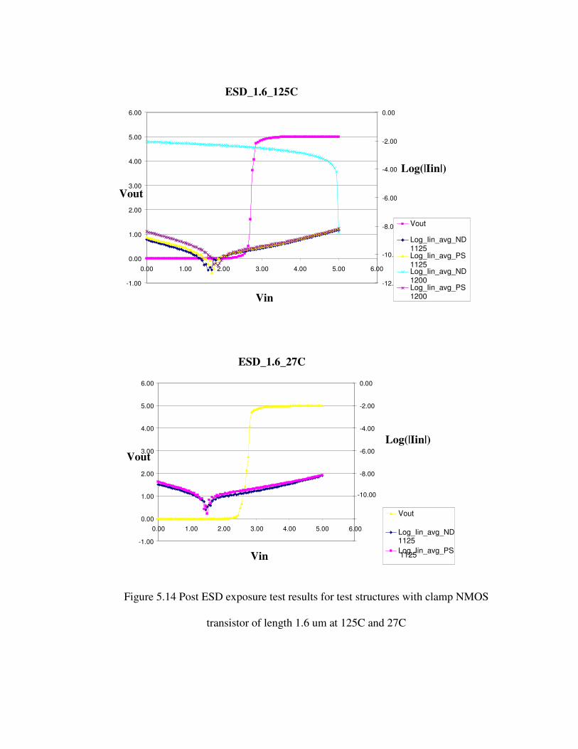
Figure 5.14 Post ESD exposure test results for test structures with clamp NMOS
transistor of length 1.6 um at 125C and 27C
ESD_1.6_125C
-1.00
0.00
1.00
2.00
3.00
4.00
5.00
6.00
0.00 1.00 2.00 3.00 4.00 5.00 6.00
Vin
Vout
-12.00
-10.00
-8.00
-6.00
-4.00
-2.00
0.00
Log(|Iin|)
Vout
Log_Iin_avg_ND 1125 Log_Iin_avg_PS 1125 Log_Iin_avg_ND 1200 Log_Iin_avg_PS 1200
ESD_1.6_27C
-1.00
0.00
1.00
2.00
3.00
4.00
5.00
6.00
0.00 1.00 2.00 3.00 4.00 5.00 6.00
Vin
Vout
-14.00
-12.00
-10.00
-8.00
-6.00
-4.00
-2.00
0.00
Log(|Iin|)
Vout
Log_Iin_avg_ND 1125 Log_Iin_avg_PS1125

5.4.7 Conclusions on ESD robustness
The test structures were found to be robust up to 1300V at room temperature and up to
1125 volts at 125°C for the worst case ESD test modes (PS and ND). It implies that the
NMOS clamp transistors are not able to sink all the ESD current and hence are
responsible of not being able to hold the voltage at the gates of the input buffer, below
8.5V which is the oxide break down strength of our NMOS and PMOS devices as
mentioned in Chapter 2 (see figure 2.7).As a result we need wider NMOS transistors with
greater number of fingers ensuring increased number of parallel paths for the ESD
currents to sink. The test results showing the ESD failure at peak ESD voltage of 1125V
call for better clamping techniques in order to increase robustness to higher ESD peak
voltages and to speed up the time taken to clamp down to voltages lower than gate oxide
break down voltage.
5.5 Characterization of I/O Pads
The methodology followed for the pads was same as it was for the Standard Cells. The
difference lies in the drive strengths. The pads were designed to drive loads as large as
160pF [Appendix A]. This huge load size demands for large transient simulation times
(1us as compared to 100ns for standard cells) which is fed in the Set up file (See Figure
3.5).also see Appendix B, look for A sample Set up File for Pads .
It was observed that while using Signal Storm for characterization, a complex cell is not
recognized and it generated some garbage timing values for the corresponding standard
cell or I/O pad cell. In our case it was the pads with tristate functionalities and also the

90
pads with active pull-up or pull-down circuit [Appendix 1].This was confirmed while
reading the .lib file format generated by signal storm (see Figure 3.5). The command that
was followed to read the .lib file in Unix environment was:-
bgx_shell > read_dotlib filename
This was followed by corrections completed in the sub-circuit file that is input to the
library characterizer. Since the pull-up and pull-down transistors affect the timing of the
I/O cells very little, they were removed from the sub-circuit files to generate the error free
timing in the .lib format.
5.6 Abstraction of I/O Pads
The abstraction of I/O pads followed the same methodology as mentioned in Chapter 3
(see section 3.6) except in the extraction and abstraction steps of the Abstract generator.
(see section 3.6.5). The steps to abstraction of I/O pads are detailed in Appendix C.
It is important here to state that the pins that at the input to the Tristate pads and output
pads, are supposed to be created at the input edge of the pad so as avoid problems
encountered by Place and Route tool. The Pin metal is extended to the edge of the input
side of the pad and this facilitates convenience to the PNR tool for locating the input pin
and routing it.

CHAPTER 6 Conclusion and Future Work
6.1 Conclusion
5V Digital Standard Cell Library and I/O Cell Library have been developed for ASIC
operable up to 125°C.The exhaustive libraries consist of 430 standard cells and 39 I/O
cells with different drive strengths. Output pads in I/O library are capable of driving 10pF
- 160pF load with a normalized output slew of 25ns. Both the libraries have been
characterized for timing and power, and abstracted for use with the place and route tool.
The Cell library has been validated on silicon using delay chain modules at 27°C and
125°C which is explained in Chapter 4. The input pad test structures have been designed
and tested for their robustness to ESD at room temperature and at 125°C for the Human
Body Model. The entire test plan and results are shown in Chapter5.
6.2 Future Work
The protection circuitry used in the I/O cell Library can be improved by using different
voltage clamping techniques between the power and ground supply rails. Better voltage
clamping techniques refers to such techniques that can clamp to voltage levels that are
lower than gate oxide break down voltage (8.5V in our case) and more importantly they
should be fast in clamping to lower voltages (than 8.5V)

Appendix A
Library Cells and Drive Strengths Specification
The definition of a 1X gate by drive is the current provided by an inverter comprised of a
1.8um/0.8um RP device and a 1.4um/1.6um RN device while by load it is the capacitance
presented by the same 1X inverter or approximately 12fF. By way of example a nand2 or
AND2X1 presents a load of approximately 21fF or approximately 1.6 loads. Note to
develop a 1X drive with AND2X1 the NMOS devices must be 2X wider, this along with
the some what longer NMOS devise account for the loading being slightly larger than
normally loading. NOR2X2 loading is 36fF or 2.7 loads.
1. Drive Strengths
• For inverters, clock tree buffers, and buffers: 1X, 2X, 3X, 4X, 6X, 8X, 12X, 16X
• Three State Buffers/Inverting and noninverting: 1X, 2X, 3X, 4X and 8X.
2. For others: Four drive strengths: 1X, 2X, 3X and 4X, where typical 2X through
4X loads are 24fF, 36fFand 48fF respectively.
3. Core Cell List
• See cell count after list.
Table 1: List of core cells
CELL TYPE CELL NAME FUNCTION
Inverters inv_X Y = not (A)
Buffers buf_X Y = A
Tie high/low tiehigh, tielow Y = VDD, Y = VSS
nand2_X Y = not (A.B)
nand3_X Y = not (A.B.C)
NAND gates
nand4_X Y = not (A.B.C.D)
nor2_X Y = not (A+B)
nor3_X Y = not (A+B+C)
NOR gates
nor4_X Y = not (A+B+C+D)
and2_X Y = A.B
and3_X Y = A.B.C
AND gates
and4_X Y = A.B.C.D
or2_X Y = A+B
or3_X Y = A+B+C
OR gates
or4_X Y = A+B+C+D

93
CELL TYPE CELL NAME FUNCTION
XOR gates xor_X Y = A⊕B
XNOR gates xnor_X Y = not(A⊕B)
ao21_X Y = (A0.A1)+B0
ao22_X Y = (A0.A1)+(B0.B1)
ao211_X Y = (A0.A1)+B0+C0
ao221_X Y = (A0.A1)+(B0.B1)+C0
ao222_X Y = (A0.A1)+(B0.B1)+(C0.C1)
ao31_X Y = (A0.A1.A2)+B0
ao32_X Y = (A0.A1.A2)+(B0.B1)
ao33_X Y = (A0.A1.A2)+(B0.B1.B2)
ao311_X Y = (A0.A1.A2)+B0+C0
ao321_X Y = (A0.A1.A2)+(B0.B1)+C0
ao331_X Y = (A0.A1.A2)+(B0.B1.B2)+C0
ao322_X Y = (A0.A1.A2)+(B0.B1)+(C0.C1)
ao332_X Y = (A0.A1.A2)+(B0.B1.B2)+(C0.C1)
AO gates
ao333_X Y = (A0.A1.A2)+(B0.B1.B2)+(C0.C1.C2)
oa21_X Y = (A0+A1).B0
oa22_X Y = (A0+A1).(B0+B1)
oa211_X Y = (A0+A1).B0.C0
oa221_X Y = (A0+A1).(B0+B1).C0
oa222_X Y = (A0+A1).(B0+B1).(C0+C1)
oa31_X Y = (A0+A1+A2).B0
oa32_X Y = (A0+A1+A2).(B0+B1)
oa33_X Y = (A0+A1+A2).(B0+B1+B2)
oa311_X Y = (A0+A1+A2).B0.C0
oa321_X Y = (A0+A1+A2).(B0+B1).C0
oa331_X Y = (A0+A1+A2).(B0+B1+B2).C0
oa322_X Y = (A0+A1+A2).(B0+B1).(C0+C1)
oa332_X Y = (A0+A1+A2).(B0+B1+B2).(C0+C1)
OA gates
oa333_X Y = (A0+A1+A2).(B0+B1+B2).(C0+C1+C2)
aoi21_X Y = not((A0.A1)+B0)
aoi22_X Y = not((A0.A1)+(B0.B1))
aoi211_X Y = not((A0.A1)+B0+C0)
aoi221_X Y = not((A0.A1)+(B0.B1)+C0)
AOI gates
aoi222_X Y = not((A0.A1)+(B0.B1)+(C0.C1))

94
CELL TYPE CELL NAME FUNCTION
aoi31_X Y = not((A0.A1.A2)+B0)
aoi32_X Y = not((A0.A1.A2)+(B0.B1))
aoi33_X Y = not((A0.A1.A2)+(B0.B1.B2))
aoi311_X Y = not((A0.A1.A2)+B0+C0)
aoi321_X Y = not((A0.A1.A2)+(B0.B1)+C0)
aoi331_X Y = not((A0.A1.A2)+(B0.B1.B2)+C0)
aoi322_X Y = not((A0.A1.A2)+(B0.B1)+(C0.C1))
aoi332_X Y = not((A0.A1.A2)+(B0.B1.B2)+(C0.C1))
aoi333_X Y =
not((A0.A1.A2)+(B0.B1.B2)+(C0.C1.C2))
oai21_X Y = not((A0+A1).B0)
oai22_X Y = not((A0+A1).(B0+B1))
oai211_X Y = not((A0+A1).B0.C0)
oai221_X Y = not((A0+A1).(B0+B1).C0)
oai222_X Y = not((A0+A1).(B0+B1).(C0+C1))
oai31_X Y = not((A0+A1+A2).B0)
oai32_X Y = not((A0+A1+A2).(B0+B1))
oai33_X Y = not((A0+A1+A2).(B0+B1+B2))
oai311_X Y = not( (A0+A1+A2).B0.C0)
oai321_X Y = not( (A0+A1+A2).(B0+B1).C0)
oai331_X Y = not( (A0+A1+A2).(B0+B1+B2).C0)
oai322_X Y = not( (A0+A1+A2).(B0+B1).(C0+C1))
oai332_X Y = not(
(A0+A1+A2).(B0+B1+B2).(C0+C1))
OAI gates
oai333_X Y = not(
(A0+A1+A2).(B0+B1+B2).(C0+C1+C2))
mux21_X Multiplexer 2 to 1
muxi21_X Multiplexer 2 to 1 with inverted output
muxi41_X Multiplexer 4 to 1
Multiplexers
muxI41_X Multiplexer 4 to 1 with inverted output
msdff_X D-type flip-flop with positive clock edge
msdffnr_X D-type flip-flop with positive clock edge and
negative asynchronous reset
Flip-Flops
msdffns_X D-type flip-flop with positive clock edge and
negative asynchronous set

95
CELL TYPE CELL NAME FUNCTION
msdffnrns_X D-type flip-flop with positive clock edge and
negative asynchronous reset and set
msdffn_X D-type flip-flop with negative clock edge
msdffnnr_X D-type flip-flop with negative clock edge and
negative asynchronous reset
msdffnns_X D-type flip-flop with negative clock edge and
negative asynchronous set
msdffnnrns_X D-type flip-flop with negative clock edge and
negative asynchronous reset and set
scanmsdff_X D-type flip-flop with positive clock edge with
scan inputs
scanmsdffnr_X D-type flip-flop with positive clock edge and
negative asynchronous reset with scan inputs
scanmsdffns_X D-type flip-flop with positive clock edge and
negative asynchronous set with scan inputs
scanmsdffnrns_
X
D-type flip-flop with positive clock edge and
negative asynchronous reset and set with scan
inputs
scanmsdffn_X D-type flip-flop with negative clock edge with
scan inputs
scanmsdffnnr_
X
D-type flip-flop with negative clock edge and
negative asynchronous reset with scan inputs
scanmsdffnns_
X
D-type flip-flop with negative clock edge and
negative asynchronous set with scan inputs
Scan Flip-Flops
scanmsdffnrnns
_X
D-type flip-flop with negative clock edge and
negative asynchronous reset and set with scan
inputs
latch_X D-type transparent latch with positive clock
level
latchnr_X D-type transparent latch with positive clock
level and negative asynchronous reset
latchns_X D-type transparent latch with positive clock
level and negative asynchronous set
Latches
latchnrns_X D-type transparent latch with positive clock
level and negative asynchronous reset and set

96
CELL TYPE CELL NAME FUNCTION
latchn_X D-type transparent latch with negative clock
level
latchnnr_X D-type transparent latch with negative clock
level and negative asynchronous reset
latchnns_X D-type transparent latch with negative clock
level and negative asynchronous set
latchnnrns_X D-type transparent latch with negative clock
level and negative asynchronous reset and set
Clock Tree Buffers Use buf_X Y = A
Three State Buffers Tribuf_X Y = A.E; Y=HiZ for not E
Three State Inv.
Buffers
Tribufi_X Y = not(A.E); Y=HiZ for not E
Table 2: Core cell count
Cell Type Number of Logic Types Total Number of Cells
Inverters 1 8
Buffers 1 8
Clkbuffers 1 8
3-State Buffers/Inverting 2 12
Tie_high/low 2 2
NAND 3 12
NOR 3 12
AND 3 12
OR 3 12
XOR 1 4
XNOR 1 4
AO 14 56
OA 14 56
AOI 14 56
OAI 14 56
MUX 4 16
Flip-Flops 8 32
Scan Flip-Flops 8 32
Latches 8 32
TOTAL 105 430

4. IO List
• See cell count at the end of list
• IO cells
o Input = pad with ESD structure and level shifter (e.g. CMOS),
optional pull-up or pull-down.
o Output = pad with ESD structure, output transistors, drivers, and
level shifter as needed.
o Bidirectional pads are made as a unification of the input and
output pads
• Input buffers have 5 drive strengths like the core cells: 1X, 2X, 3X, 4X
and 7X, where typical 2X through 7X loads are 24fF, 36fF, 48fF and
144fF respectively.
• Output buffers have 5 drive strengths: 1.6mA, 3.2mA, 4.8mA, 8.00mA
and 12.8mA (<25nS rise/fall times into 20pF, 40pF, 80pF, 120pF, and
160pF loads.)
• Outputs buffers have 1 normalized slew rate. 25ns
o Bidirectional pads have 1 normalized slew rate with CMOS inputs with
optional pull-up or pull-down.
Table 3: IO cell count
Cell Type Number of Logic Types Total Number of Cells
PAD_BIDIR_CMOS 3 15
PAD_IN_CMOS 3 15
PAD_OUT 1 5
VDD Pad (Pvdd) 1 1
VSS Pad (Pvss) 1 1
Corner Pad (Pcorner_dec) 1 1
Decoupling Pad(Pfill5) 1 1
TOTAL 12 39

Appendix B
Inputs to SignalStorm library Characterizer
A sample sub-circuit (netlist – aoi322_4) file as an input to SignalStorm
simulator lang=spectre
global 0
include "/export/home/liuc/pscmodel/tol.scs"
// Library name: Navy_Cells
// Cell name: aoi322_4
// View name: schematic
subckt aoi322_4 A B C D E F G VDDD VSSD Y
M39 (Y net74 VSSD) rnx w=5.6u l=1.6u mt=1
M40 (net74 net62 VSSD) rnx w=1.4u l=1.6u mt=1
M41 (net71 E VSSD) rnx w=2.8u l=1.6u mt=1
M53 (net62 F net50) rnx w=2.8u l=1.6u mt=1
M54 (net62 D net71) rnx w=2.8u l=1.6u mt=1
M55 (net62 A net59) rnx w=4.2u l=1.6u mt=1
M56 (net59 B net56) rnx w=4.2u l=1.6u mt=1
M57 (net56 C VSSD) rnx w=4.2u l=1.6u mt=1
M59 (net50 G VSSD) rnx w=2.8u l=1.6u mt=1
M52 (Y net74 VDDD) rp w=7.2u l=800n mt=1
M60 (net74 net62 VDDD) rp w=1.8u l=800n mt=1
M61 (net62 F net82) rp w=4.5u l=800n mt=1
M62 (net82 E net95) rp w=4.5u l=800n mt=1
M63 (net95 A VDDD) rp w=4.5u l=800n mt=1
M64 (net95 B VDDD) rp w=4.5u l=800n mt=1
M65 (net95 C VDDD) rp w=4.5u l=800n mt=1
M67 (net62 G net82) rp w=4.5u l=800n mt=1
M68 (net82 D net95) rp w=4.5u l=800n mt=1
ends aoi322_4
// End of subcircuit definition.

A sample Setup file- for standard cells in typical process
Look for different aspects of the simulation to be run by SignalStorm, ex transient
time, Process, Binary search , load, slew mentioned in Chapter 3.
Process typical{
voltage = 5 ;
temp = 27 ;
Corner = "tt" ;
Vtn = 0.755 ;
Vtp = 0.654 ;
};
Signal std_cell {
unit = REL;
Vh=1.0 1.0;
Vl=0.0 0.0;
Vth=0.5 0.5;
Vsh=0.9 0.9;
Vsl=0.1 0.1;
tsmax=10.0n;
};
Simulation std_cell{
transient = 0.1n 50n 50p;
//(start, stop, step)
dc = 0.26 5 0.03;
bisec = 12.0n 12.0n 150p;
//
resistance = 10MEG;
};
Index X1{
Slew = 1n 2n 4n 6n 8n;
// Input slews 10 to 90%
Load = 0.005p 0.013p 0.026p 0.04p 0.052p 0.104p;
// Output load capacitances nx1X, nx2X, nx3X, nx4X and nx8X
//for a nX drive, n = 1 in the above example.
};
Index X2{
Slew = 1n 2n 4n 6n 8n;
Load = 0.005p 0.026p 0.052p 0.08p 0.106p 0.208p;
};
Index X3{
Slew = 1n 2n 4n 6n 8n;
Load = 0.005p 0.04p 0.078p 0.12p 0.16p 0.312p;
};
Index X4{
Slew = 1n 2n 4n 6n 8n;
Load = 0.005p 0.052p 0.104p 0.16p 0.212p 0.416p;

100
};
Index X5{
Slew = 1n 2n 4n 6n 8n;
Load = 0.005p 0.065p 0.130p 0.2p 0.260p 0.520p;
};
Index X6{
Slew = 1n 2n 4n 6n 8n;
Load = 0.005p 0.08p 0.156p 0.24p 0.32p 0.624p;
};
Index X7{
Slew = 1n 2n 4n 6n 8n;
Load = 0.005p 0.091p 0.182p 0.273p 0.364p 0.728p;
};
Index X8{
Slew = 1n 2n 4n 6n 8n;
Load = 0.005p 0.104p 0.208p 0.32p 0.424p 0.832p;
};
Index X9{
Slew = 1n 2n 4n 6n 8n;
Load = 0.005p 0.117p 0.234p 0.351p 0.468p 0.936p;
};
Index X10{
Slew = 1n 2n 4n 6n 8n;
Load = 0.005p 0.130p 0.26p 0.39p 0.52p 1.04p;
};
Index X11{
Slew = 1n 2n 4n 6n 8n;
Load = 0.005p 0.143p 0.286p 0.429p 0.572p 1.114p;
};
Index X12{
Slew = 1n 2n 4n 6n 8n;
Load = 0.005p 0.158p 0.316p 0.474p 0.632p 1.264p;
};
Index X14{
Slew = 1n 2n 4n 6n 8n;
Load = 0.005p 0.185p 0.370p 0.554p 0.739p 1.478p;
};
Index X15{
Slew = 1n 2n 4n 6n 8n;
Load = 0.005p 0.198p 0.396p 0.594p 0.792p 1.584p;

101
};
Index X18{
Slew = 1n 2n 4n 6n 8n;
Load = 0.005p 0.238p 0.475p 0.713p 0.950p 1.90p;
};
Index X20{
Slew = 1n 2n 4n 6n 8n;
Load = 0.005p 0.264p 0.528p 0.792p 1.056p 2.112p;
};
Index X22{
Slew = 1n 2n 4n 6n 8n;
Load = 0.005p 0.29p 0.58p 0.871p 1.160p 2.323p;
};
Index X24{
Slew = 1n 2n 4n 6n 8n;
Load = 0.005p 0.317p 0.634p 0.950p 1.270p 2.53p;
};
Index Clk_Slew{
bslew = 0.5n 2n 10.0n;
};
Group X1{
CELL = *1;
};
Group X2{
CELL = *2;
};
Group X3{
CELL = *3;
};
Group X4{
CELL = *4;
};
Group X5{
CELL = *5;
};
Group X6{
CELL = *6;
};
Group X7{
CELL = *7;
};
Group X8{
CELL = *8;
};
Group X9{

102
CELL = *9;
};
Group X10{
CELL = *10;
};
Group X11{
CELL = *11;
};
Group X12{
CELL = *12;
};
Group X14{
CELL = *14;
};
Group X15{
CELL = *15;
};
Group X18{
CELL = *18;
};
Group X20{
CELL = *20;
};
Group X22{
CELL = *22;
};
Group X24{
CELL = *24;
};
Group X1a{
CELL = *1a;
};
Group X5a{
CELL = *5a;
};
Group Clk_Slew{
PIN = *.CLK ;
};
Margin m0 {
setup = 1.0 0.0 ;
hold = 1.0 0.0 ;
release = 1.0 0.0 ;
removal = 1.0 0.0 ;

103
recovery = 1.0 0.0 ;
width = 1.0 0.0 ;
delay = 1.0 0.0 ;
power = 1.0 0.0 ;
cap = 1.0 0.0 ;
} ;
Nominal n0 {
delay = 0.5 0.5 ;
power = 0.5 0.5 ;
cap = 0.5 0.5 ;
} ;
set process(typical){
simulation = std_cell;
signal = std_cell;
margin = m0;
nominal = n0;
};
set index(typical){
Group(X1) = X1;
Group(X2) = X2;
Group(X3) = X3;
Group(X4) = X4;
Group(X5) = X5;
Group(X6) = X6;
Group(X7) = X7;
Group(X8) = X8;
Group(X9) = X9;
Group(X10) = X10;
Group(X11) = X11;
Group(X12) = X12;
Group(X14) = X14;
Group(X15) = X15;
Group(X18) = X18;
Group(X20) = X20;
Group(X22) = X22;
Group(X24) = X24;
Group(X1a) = X1;
Group(X5a) = X5;
Group(Clk_Slew) = Clk_Slew;
};

104
A sample Step file or batch file, which is used to specify the commands and set
values to SignalStorm-
Look for the command in bold – specifies the sub-circuit filename (Appendix A .1. )
and the set up file name (Appendix A. 2.)
set_var SG_SPICE_SUPPLY1_NAMES "VDDD"
set_var SG_SPICE_SUPPLY0_NAMES "VSSD"
set_var SG_SPICE_SIMPLIFY true
set_var SG_SIM_TYPE "spectre"
set_var SG_CASE_SENSITIVITY 1
db_open typical
db_install -subckt aoi_m.scs -model model_tt.scs
db_gsim -force
db_setup -s setup_typical.ss
db_spice -p typical -keep_log

Appendix C
ABSTRACTION TUTORIAL
1. Attach the standard cell library to the existing technology library pscPNR which
stands for Peregrine Semiconductor Place and Route library.
2. Only layout and logical views are required to generate abstract views. So it is
suggested that all the views are copied to a new library and then attached to the
P&R technology library.
3. Open the layout of any cell and go to Tools � Abstract Generator


4. The display on the layout window shows a tab of Abstract. Go to Abstract�
Create Abstract.
5. An abstract generator GUI will pop up and load up all the cells in the window.

108
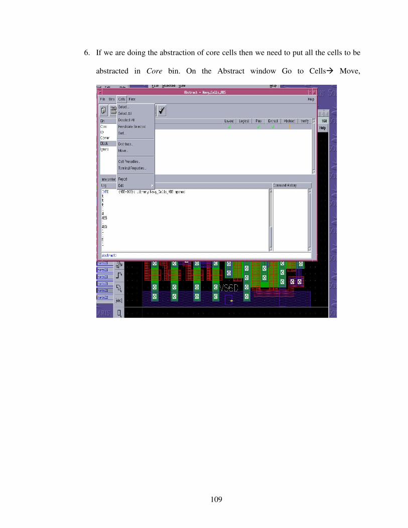
109
6. If we are doing the abstraction of core cells then we need to put all the cells to be
abstracted in Core bin. On the Abstract window Go to Cells� Move,

110
7. a window pops up prompting the user to select the bin where he needs to move
the cell. Select Core.

111
8. Select the cell/cells in the core bin and start the steps to generate Abstract view.
9. Choose Flow � Pins

112
• Choose the Map tab, On the Map tab you can specify the text labels to be
used for creating starting pin shapes for each of the nets to be extracted.
You can also specify Pins that are power (VDDD), ground (VSSD), clock,
analog or output pins. Unless there are terminals already present one must
specify a value in Map text labels to pins field to generate a valid pins
view. Note: - If the field is left empty, the abstract generator automatically
assumes a default value for the field before proceeding.

113
• Choose the Text tab.
The text tab allows you to change the name of the pins created in the Pins
view from the original value in the layout. The field ‘Label search depth’ and
‘Geometry search depth’ allows you to specify the search depth for labels and
geometries. The default values are 0 and 20 respectively. Keep them at default
values. By default, the option of preserving the text labels is disabled. If you
want the text labels from the layout to be retained in the final abstract then
you might consider enabling this option.

114
• Choose the Boundary tab
The options in the Boundary tab control the calculation of the place-and-route
(PR) boundary, which defines the size of a single cell. Specify the creation of
the PR Boundary to always.

115
Leave the Adjust Boundary and Fix Boundary sections empty unless you want
to fix individual cell boundary edges. Since we are abstracting all the cells at
the same time, fixing a value in Fix Boundary or Adjust Boundary sections is
not recommended.

116
• Choose the Blocks tab
The options on the Blocks tab are intended for use with any layout view that
has existing routing. Typically it is used for routed blocks, so we don’t need
this as we are abstracting standard cell layouts. If you are using blocks then
you can check preserve local blockages in routed blocks and also enable the
create Power Pins from routing option. Look at the following snapshot.

117
• Now click RUN to run the PIN step.Look for a � ‘√’ or ‘!’ for a correct
running of the step – PIN. Its an error if ‘x’ shows up.
10. Go to Flow � Extract
This step extracts each terminal net.
• Choose the Signal tab
Check the Extract signal Option while abstracting the standard cells and
disable it while abstracting IO cells..
The Signal tab allows you to view and modify the options for extracting signal
nets. You can specify the layers through which you want the abstract
generator to extract, the layers on which pins are to be created, the limits of
extraction, and the way in which must-connect relationships are to be handled.
Choose the Connectivity to be Strong and check the create Pins options.

118
• Select the Power Tab
Check the Extract Power nets option when abstracting Standard Cells. It is on
by default when abstracting standard cells and not for IO cells.
Mention the names of the layers under the Layer field and also check the
Create Pins option.

119
• elect the Antenna tab
It is disabled by default and is recommended to be switched off by the
Cadence Abstract Generator for standard cells and IO cells.
.

120
• Select General
The Layer connectivity field is used to specify the connectivity between
layers. This allows you to specify the layer connectivity without having to add
via definitions in the technology file.

121
• Now select Run tab in the extract window. Look for a � ‘√’ or ‘!’ for a
correct running of the step – Extract. Its an error if ‘x’ shows up
11. Go to Flow � Abstract
• Select Adjust

122
In this tab only option available for abstraction in Core bin is to mention the
power rail widths, offsets and shape.
The nets VDDD and VSSD are provided with Shape field as abutment

123
• Select the Blockage tab
The options on this tab control the final blockage geometry in the abstract
view. The Layer column prompts the user to enter the layers on which he
wants the blockages. Enter the Geometry Specification that applies to the
blockage model (see the following snapshot) .Choose the type of blockage
you want to create on the specified layer: Cover, Detailed, or Shrink. The
default is- Detailed for the Core bin (standard cells).
A Cover blockage blocks the entire area that is not occupied by pin
shapes, effectively blocking a layer for routing. Cover blockages are
typically used on the metal1 layer for blocks or IO cells where you want to
prevent over-the-cell routing in order to improve performance or to avoid
electrical effects between tracks.
The Detailed blockage model generates blockages only where there are
real shapes in the cell on that layer. It is used for standard cells. Using the
detailed blockage model can adversely affect the performance of the
abstract generator because of the number of individual shapes that need to
be processed.
Shrink The Shrink blockage model fills in smaller, less useful free spaces
and leaves larger spaces in the cell open. This allows over-the-cell routing
without modeling each obstruction individually. The Shrink blockage
model leads to slower abstract generation but significantly faster routing
times than the- Detailed blockage model.

124
One can use the Cut window around pins large enough to drop via option
to control the size of the window cut into a blockage around a pin. This
option is selected by default. When this option is selected, the abstract
generator cuts a window large enough for a via to be dropped to that pin.

125
• Select Fracture tab
Check the Fracture Pins and Fracture Blockages option.
This option controls whether the abstract generator creates each pin /
blockage shape as a set of maximum rectangles or as a polygon. This
option is available for all bins.

126
• Select Site tab
Sites tell the placer where it can place cells. All cells that are located in a
particular bin share a common set of properties: symmetry, class (for
example, pad or core), width, and height. These properties are used by the
placer to assist in the placement process.
The site name appears based on the bin. User doesn’t need to give input
unless he wants a different Site name.

127
• Select Overlap tab.
The overlap boundary is a second, more detailed boundary used by
placement tools to test whether cells overlap. Unlike the PR boundary,

128
which is always rectangular, the overlap boundary can be a rectilinear
polygon. This helps the placement tools achieve better placement density
for certain types of standard cells and rectilinear blocks. The options on
this tab control whether the abstract generator is to update the overlap
boundary geometry.
Note: The abstract generator can create an overlap boundary only if there
is an overlap layer defined in the technology information. If there is no
overlap layer present, the abstract generator issues a warning.
You can use the Create overlap boundary option to specify whether the
abstract generator should create an overlap boundary – always, as needed
or off. Select - always.
This option is enabled when the Create overlap boundary option is set to
always or as needed. The default values depend on the current bin. The
default for the Core bin is half the minimum separation defined for the
metal1 layer. You can use this option to ensure that the placement of cells
with abutting overlap layers does not lead to geometry contained in these
cells causing violations. In our case it is 0.4.

129

130
• Select Grids tab
The options on this tab control the grid analysis function that calculates
the best metal1 and metal2 routing grid pitches and offsets for the user’s
standard cells.
Grid analysis is intended for use with standard cell Core bins for which
the default mode is report. For all other bins, the default is off, that is, no
grid reporting or calculation is done.
The four pitch and offset fields in the Routing Grid Values section on the
Grids tab show the current routing grid values. See the values in the
snapshot for our library. If the pitch mentioned by user is not in coherence
with the cell height and width, the abstract generator issues the warning
regarding a possibility of inefficient routing.

131
• Select Run on the Abstract window to run the Abstract step.
Look for a � ‘√’ or ‘!’ for a correct running of the step –Abstract. It is an
error if ‘x’ shows up.

132
12. Go to File � Export � LEF

133
• Select LEF � give a name to LEF file to be exported and click OK.

134
REFERENCES
1. J. Goetz, "High temperature electronics for sensor interface and data
acquisition," Solid State Electronics Center, Honeywell 1998.
2. V.Madhuravasal, J.Wang, C.Hutchens, X.Zhu and Y.Zhang, "High Temperature
Silicon-on-Insulator (SOI) Deep Submicron Device Performance," HITEC 2006
Conference, Santa Fe, New Mexico, May 2006.
3. “Development of a 5V digital cell library For Use With ThePeregrine
Semiconductor Silicon on Sapphire (SOS) Process”, by Usha Badam,Thesis
,Oklahoma State University,2007.
4. Michael John and Sebastian Smith, “Application-Specific Integrated Circuits”,
Addison-Wesley Publishing Company, VLSI Design Series, June 1997.
5. “SOI Technology for the GHz Era” Ghavam G; Shahidi.
6. P. McAdam and B.G. Goldberg, "CMOS SOS for Mixed Signal ICs," Peregrine
Semiconductor Corporation, June 2001.
7. SOI VS CMOS for Analog Circuit Vivian Ma, 961347420, University of Toronto

135
8. J.M. Stern, P. A. Ivey, S. Davidson, and S. N. Walker, “Silicon-On-Insulator
(SOI): A High Performance ASIC Technology,” (1992).
9. R. Howes, W.Redman-White, “A Small-Signal Model for the Frequency-
dependent Drain Admittance in Floating Substrate MOSFETs”, IEEE J. Sol. St.
Ckts, 27( 8), Aug 1992.
10. J.-P. Colinge, "Silicon-On-Insulator Technology: Materials to VLSI," 2 ed.:
Kluwer Academic Publishers, 2000.
11. “Proposal for a 3.3V/5V Low Leakage High Temperature Digital Cell Library
Usign Stacked Transistors”, by Singaravelan Vishwanathan, Oklahoma State
University 2007.
12. “CMOS VLSI Design,A Circuits and Sytems Perspective”, by Neil .H.E.Weste
and David Harris ,Third Edition.
13. “Characterizing a Cell Library Using ICCS”, Teri Hike McFaul Karl Perry, Intel
Corporation, ASIC Seminar and Exhibit, Sep 1990 Proceedings Third Annual
IEEE.
14. SignalStorm Characterization Manual

136
15. “Automated Standard Cell Library Generation & study of Cell Library Functional
Content”, Yunbum Jung, University of Michigan
16. “Comparison of ESD Protection Capability of SOI and Bulk CMOS Output
Buffers”, Mansun Chan, Selina S. Yuen, Zhi-Jian Ma, Kelvin Y. Hui, Ping K. KO
and Chenming Hu Department of Electrical Engineering and Computer Science
University of California at Berkeley.
17. “Application Report SSYA010” - January 2001, Electrostatic Discharge (ESD)
18. “SILICON ON INSULATOR TECHNOLOGY: Materials toVLSI,2nd
Edition”,
Jean-Pierre Colinge, Kluwer Academic Publishers
19. “Method and Structure for Providing ESD Protection for Silicon On Insulator
Integrated Circuits”, David R. Staab, Sheau-Suey Li, United States Patent , Patent
number- 5610,790.
20. “ Fundamentals Of ESD” , Part Five – Device Sensitivity and Testing , 2001,
ESD association, Rome, NY

VITA
Vibhor Jain
Candidate for the Degree of
Master of Science
Thesis: DESIGN OF 5V DIGITAL STANDARD CELLS AND I/O LIBRARIES FOR
MILITARY STANDARD TEMPERATURES
Major Field: Electrical and Computer Engineering
Biographical:
Personal Data: Born in Neemuch, (M.P) India on August 16th
, 1983 the son of Mr.
Keshrimal Jain and Mrs. Vimla Jain.
Education: Graduated from higher secondary school in Kota, India; received a
bachelor’s degree from Devi Ahilya University, India in May 2006
in the field of Electronics & Instrumentation Engineering.
Completed the requirements for the Master of Science degree with a
major in Electrical & Computer Engineering at Oklahoma State
University in July, 2008.z
Experience: Worked as a Graduate Research Assistant in Mixed Signal VLSI
Design Lab in Department of Electrical & Computer Engineering at
Oklahoma State University from January 2007 to March 2008.
Worked as a Graduate Assistant in the Department of Electrical
Engineering and Technology, University Research Compliance at
Oklahoma State University from October 2006 to July 2008.

Name: Vibhor Jain Date of Degree: July, 2008
Institution: Oklahoma State University Location: Stillwater, Oklahoma
Title of Study: DESIGN OF 5V DIGITAL STANDARD CELLS AND I/O LIBRARIES
FOR MILITARY STANDARD TEMPERATURES
Pages in Study: 136 Candidate for the Degree of Master of Science
Major Field: Electrical Engineering
Scope and Method of Study:
The scope of this research work is to develop digital standard cell and I/O cell
libraries operable at 5V power supply and operable up to 125°C using Peregrine
0.5um 3.3 V process. Device geometries are selected based on Ion/Ioff ratios at
125°C. The cell schematic, layout and abstracted views are generated for both the
libraries The Standard cell and I/O libraries are characterized for timing and
power and the characterization data is realized in various formats compatible with
logic synthesis and place and route tools. The pads have been tested for
robustness to ESD. A tutorial on abstraction of standard cells and IO cells is
prepared using the Cadence Abstract Generator.
Findings and Conclusions:
Three input pad test structures were designed and fabricated on a test chip, with
different lengths (1.4um, 1.5um, 1.6um) of NMOS clamp transistor to test the
robustness of the pads to ESD for a Human Body Model at 27°C and 125°C.
Measured Data shows the robustness of the pads to ESD peak voltages of 1200V
at 125°C and up to 1300V at 27°C. A test chip for delay chain with single input
and multiple input combinatorial gates was designed and fabricated as part of
validation on silicon. Measured data shows a shift across temperatures relative to
the simulation for fast process suggesting the inaccuracy in model files used for
simulation.
ADVISER’S APPROVAL: Dr. Chris Hutchens