Design fabrication and calibration of MEMS actuators for ...
112
University of New Mexico UNM Digital Repository Mechanical Engineering ETDs Engineering ETDs 1-29-2009 Design fabrication and calibration of MEMS actuators for in-situ materials testing Khawar Abbas Follow this and additional works at: hps://digitalrepository.unm.edu/me_etds is esis is brought to you for free and open access by the Engineering ETDs at UNM Digital Repository. It has been accepted for inclusion in Mechanical Engineering ETDs by an authorized administrator of UNM Digital Repository. For more information, please contact [email protected]. Recommended Citation Abbas, Khawar. "Design fabrication and calibration of MEMS actuators for in-situ materials testing." (2009). hps://digitalrepository.unm.edu/me_etds/34
Transcript of Design fabrication and calibration of MEMS actuators for ...

University of New MexicoUNM Digital Repository
Mechanical Engineering ETDs Engineering ETDs
1-29-2009
Design fabrication and calibration of MEMSactuators for in-situ materials testingKhawar Abbas
Follow this and additional works at: https://digitalrepository.unm.edu/me_etds
This Thesis is brought to you for free and open access by the Engineering ETDs at UNM Digital Repository. It has been accepted for inclusion inMechanical Engineering ETDs by an authorized administrator of UNM Digital Repository. For more information, please contact [email protected].
Recommended CitationAbbas, Khawar. "Design fabrication and calibration of MEMS actuators for in-situ materials testing." (2009).https://digitalrepository.unm.edu/me_etds/34

Khawar Abbas
Candidate
Mechanical Engineering Department
Department
This thesis is approved, and it is acceptable in quality
and form for publication on microfilm:
Approved by the Thesis Committee:
Dr. Zayd C. Leseman Committee Chair
Dr. Yu-Lin Shen Committee Member
Dr. Marwan Al-Haik Committee Member
Accepted:
Dean, Graduate School
Date

DESIGN FABRICATION AND CALIBRATION OF
MEMS ACTUATORS FOR IN-SITU MATERIALS TESTING
BY
KHAWAR ABBAS
B.E. Mechanical, National Univ. of Sc. & Tech., Pakistan, 2000
THESIS
Submitted in Partial Fulfillment of the
Requirements for the Degree of
Master of Science
Mechanical Engineering
The University of New Mexico
Albuquerque, New Mexico
December, 2008

iii
ACKNOWLEDGEMENTS
This thesis would not have been possible without the countless contributions of
so many people that I came across during my MS at the University of New
Mexico. I would like to thank them and let them know that I appreciate their help
from the bottom of my heart.
I am thankful to Allah Subhana wa Ta’ala (God the Almighty and the Greatest) for
everything that I am blessed with in life, for giving me this opportunity to learn
and answering my prayers in times of frustration and desperation when nothing is
going as planned.
I am grateful to my research advisor Dr. Zayd C. Leseman. He introduced me to
this exciting field of MEMS and Micro-mechanics, provided technical guidance,
necessary financial support and overlooked my mistakes. He has been a
constant source of inspiration for me and this work would not have been possible
without his support, encouragement and suggestions.
I am thankful for the support provided by UNM Manufacturing Training and
Technology Center (MTTC). The cleanroom staff at MTTC was extremely helpful
and insightful. Harold Madsen helped me in developing the fabrication process
and at the same time keeping myself safe from chemicals in the cleanroom. Sam
Kriser was very instrumental in keeping the equipment that I required in perfect
working order. Without their support this work would have been impossible.
Thanks to Mark Atwater for helping me out in obtaining SEM images and
measurements. I am thankful to Maheshwar R. Kashamola for letting me use his

iv
optical components for my experimental setup. I want to express my gratitude to
Dr. Lumia and his graduate student Brian Schmitt for allowing me to use their
CCD camera. Brian was also very helpful to me in maintaining my sanity in the
Lab. Our brain storming sessions were very insightful and the short trips to Cold
Stone and Dunkin’ Donuts were very helpful in boosting my morale after a failed
experiment.
I would like to thank my fellow students Drew Goettler and Edidson Lima for their
help, support, friendship and comradeship. They made me feel at home and
welcomed at the time when everything around me was totally new in a foreign
land. I wish both of them best of luck in their future endeavors.
Last, and most importantly my parents deserve much credit for my success. They
raised me in an atmosphere of appreciation of science, for learning and for
striving to understand the world around me. I am especially grateful to my mother
for her constant encouragement, unconditional support and genuine love.
I have inevitably missed some people but I would like all of them to know that
their help is no less appreciated - “Thanks a lot.”
DESIGN FABRICATION AND CALIBRATION OF
MEMS ACTUATORS FOR IN-SITU MATERIALS TESTING
BY
KHAWAR ABBAS
ABSTRACT OF THESIS
Submitted in Partial Fulfillment of the
Requirements for the Degree of
Master of Science
Mechanical Engineering
The University of New Mexico
Albuquerque, New Mexico
December, 2008

vi
DESIGN FABRICATION AND CALIBRATION OF MEMS ACTUATORS FOR IN-SITU MATERIALS TESTING
BY
KHAWAR ABBAS B.E. Mechanical, National Univ. of Sc. & Tech., Pakistan, 2000
M.S., Mechanical Engineering, University of New Mexico, 2008
ABSTRACT
Many MEMS devices utilize thin metallic films as mechanical structures. The
elastic and plastic properties of these thin films (thickness < 1µm) are
significantly different from those of the bulk material. At these scales the volume
fraction of material defects such as: grain boundaries, dislocations and
interstitials become quite significant and become a chief contributor the physical
and mechanical material properties of the thin films. Aluminum (Al), Copper
(Cu), Nickel (Ni) and Gold (Au) are popular thin film materials used in
MEMS/NEMS. Various studies have been conducted in recent years to study the
mechanical properties of freestanding thin films in situ in TEM to study their
failure mechanisms. Some of these studies utilize MEMS devices as actuators.
These actuators are often co-fabricated with the specimen being tested therefore
limiting the type of specimen that could be tested. Also these MEMS actuators
are almost never traceably calibrated and their response is calculated. This
thesis describes the design and fabrication process of a MEMS actuator for
materials testing in-situ in TEM. The actuator is fabricated independent of the
specimen. A setup was designed to calibrate these devices with a method that
can be traced back to NIST standards. It has been shown that the calibrated

vii
response of these MEMS actuators is different from its calculated response and
the use of un-calibrated devices for materials testing can lead to misleading
results.

viii
Table of Contents Chapter 1 ........................................................................................................................................ 1
1. INTRODUCTION ................................................................................................................... 1
1.1. Background and Motivation ......................................................................................... 1
1.2. Scope .............................................................................................................................. 5
1.3. Overview / Organization ............................................................................................... 5
Chapter 2 ........................................................................................................................................ 6
2. THEORY OF MEMS COMB DRIVE ACTUATORS ......................................................... 6
2.1. Flexure Springs.............................................................................................................. 6
2.1.1. Fixed-fixed flexure ..................................................................................................... 7
2.1.2. Crab-Leg Flexure .................................................................................................... 11
2.1.3. Folded Flexure ......................................................................................................... 13
2.1.4. Serpentine Flexure .................................................................................................. 16
2.2. Electrostatic Force ...................................................................................................... 18
2.2.1. Side (Axial) Instability ............................................................................................. 20
2.2.2. Front (Lateral) Instability......................................................................................... 21
Chapter 3 ...................................................................................................................................... 23
3. DESIGN AND FABRICATION ........................................................................................... 23
3.1. Design specifications .................................................................................................. 23
3.2. Fabrication .................................................................................................................... 28
3.2.1. Mask Design and Development ............................................................................ 28
3.2.2. Actuator Fabrication ................................................................................................ 28
Chapter 4 ...................................................................................................................................... 33
4. TESTING AND CALIBRATION ......................................................................................... 33
4.1. Side Instability Voltage ............................................................................................... 33
4.1.1. Setup ......................................................................................................................... 33
4.1.2. Procedure ................................................................................................................. 35
4.2. Calibration .................................................................................................................... 35
4.2.1. Setup ......................................................................................................................... 38
4.2.2. Procedure ................................................................................................................. 41
Chapter 5 ...................................................................................................................................... 45
5. EXPERIMENTAL RESULTS AND DISCUSSION .......................................................... 45

ix
5.1. Compressive Residual Forces .................................................................................. 45
5.2. Side Instability Voltage ............................................................................................... 46
5.3. Calibration .................................................................................................................... 47
5.3.1. Fixed-fixed flexure ................................................................................................... 49
5.3.2. Folded flexure .......................................................................................................... 53
Chapter 6 ...................................................................................................................................... 56
6. CONCLUSION ..................................................................................................................... 56
6.1. Future Work.................................................................................................................. 57
Bibliography ................................................................................................................................. 58
Appendix ‘A’ ................................................................................................................................. 62
A. FABRICATION PROCEDURE .......................................................................................... 62
Appendix ‘B’ ................................................................................................................................. 65
B. MATLAB CODES ................................................................................................................ 65
Appendix ‘C’ ................................................................................................................................. 82
C. TEM HOLDER DESIGN DRAWINGS .......................................................................... 82

x
List of Figures
FIGURE 1: (A) FIXED-FIXED FLEXURE DESIGN. (B) FREE BODY DIAGRAM OF A FIXED-FIXED
BEAM ........................................................................................................................ 8
FIGURE 2: DEFLECTION OF FIXED-FIXED BEAM WITH DIMENSION (H X B X 2L) ......................10
FIGURE 3: CRAB-LEG FLEXURE DESIGN ............................................................................11
FIGURE 4: DEFLECTION OF CRAB-LEG FLEXURE (IN Y- DIRECTION) WITH DIMENSIONS LA =
500µM LB = 50µM WA = WB =2µM AND T=20UM .........................................................13
FIGURE 5: FOLDED FLEXURE DESIGN ................................................................................14
FIGURE 6: DEFLECTION OF FOLDED FLEXURE ( IN Y-DIRECTION) WITH DIMENSIONS LT =
500µM; LB 50µM WT = WB =2µM AND T=20UM ...........................................................15
FIGURE 7: DESIGN OF SERPENTINE FLEXURE ....................................................................16
FIGURE 8: DEFLECTION OF SERPENTINE FLEXURE (IN Y-DIRECTION) WITH DIMENSIONS A =
20µM, B = 20µM, W = 2µM, N = 20 AND T = 20µM .........................................................18
FIGURE 9: SCHEMATIC DETAILS OF COMB FINGERS. ...........................................................19
FIGURE 10: SCHEMATIC DESIGN OF A COMB DRIVE ACTUATOR WITH FIXED-FIXED FLEXURE .26
FIGURE 11: SCHEMATIC OF A CUSTOM SPECIMEN HOLDER FOR JEOL 2010 AND THE
PLACEMENT OF THE MEMS DEVICE ...........................................................................27
FIGURE 12: CUSTOM MANUFACTURED TEM HOLDER .........................................................27
FIGURE 13: A SCHEMATIC SHOWING THE FABRICATION PROCESS OF THE MEMS ACTUATOR 30
FIGURE 14: OPTICAL MICROGRAPH OF THE ACTUATOR WITH FIXED-FIXED FLEXURE, L=800,
N=600 .....................................................................................................................31

xi
FIGURE 15: OPTICAL MICROGRAPH OF THE ACTUATOR WITH SERPENTINE FLEXURE AND
N=600 .....................................................................................................................31
FIGURE 16: OPTICAL MICROGRAPH OF THE ACTUATOR WITH FOLDED FLEXURE AND N=2000 32
FIGURE 17: EXPERIMENTAL SETUP USED TO DETERMINE THE SIDE INSTABILITY ...................34
FIGURE 18: PROBE TIPS IN CONTACT WITH BONDING PADS OF A MEMS ACTUATOR .............34
FIGURE 19: MEMS ACTUATOR MOUNTED ON THE GLASS SLIDE ..........................................38
FIGURE 20: GLASS SLIDE MOUNTED ON THE GONIOMETER AND INDEPENDENT LINEAR STAGE
FOR MOVEMENT IN Z-DIRECTION ................................................................................39
FIGURE 21: MICROSCOPE MOUNTED ON SEPARATE LINEAR STAGES FOR INDEPENDENT X-Y-Z
MOVEMENT ..............................................................................................................39
FIGURE 22: THE COMPLETE CALIBRATION SETUP ...............................................................40
FIGURE 23: OPTICAL MICROGRAPH OF 790 µM SAPPHIRE SPHERE ATTACHED TO THE
ACTUATOR ...............................................................................................................42
FIGURE 24: ACTUATOR TIP DIPPED IN PHOTORESIST DROPLET ...........................................44
FIGURE 25: OPTICAL MICROGRAPH OF THE STRAIN GUAGE AT THE CENTRE OF THE WAFER ..46
FIGURE 26: CALIBRATION CURVE FOR THE FIXED-FIXED FLEXURE .......................................50
FIGURE 27: RANGE OF UNCERTAINTY IN ACTUATOR RESPONSE WITH ELASTIC MODULUS 150 –
170 GPA .................................................................................................................52
FIGURE 28: COMPARISON BETWEEN THE CALIBRATED RESPONSE AND THE UNCERTAINTY DUE
TO DIMENSIONAL VARIATION OF DEVICE WITH FIXED-FIXED FLEXURE ............................52
FIGURE 29: CALIBRATION CURVE FOR THE FOLDED FLEXURE .............................................53

xii
FIGURE 30: RANGE OF UNCERTAINTY IN ACTUATOR RESPONSE WITH ELASTIC MODULUS 150 –
170 GPA .................................................................................................................54
FIGURE 31: COMPARISON BETWEEN THE CALIBRATED RESPONSE AND THE UNCERTAINTY DUE
TO DIMENSIONAL VARIATION OF DEVICE WITH FOLDED FLEXURE ...................................55

1
Chapter 1
1. INTRODUCTION
1.1. Background and Motivation
Advancements in the semiconductor fabrication technology particularly the
advancement in bulk and surface micromachining techniques of silicon (Si)
during the 1980’s and early 1990’s opened doors to a new era of miniaturized
electro-mechanical structures and devices that are now known as “MEMS (Micro
Electro-Mechanical Systems)” [1-5]. These devices offered new capabilities,
improved performance and lower cost due to batch production over traditional
transducers and sensors. Perhaps the greatest advantage that MEMS had to
offer was their ability to be fabricated compatibly with an integrated circuit (IC)
thereby reducing the overall size and power requirements of a complete system
to that of a mere IC chip. Since then, this field of science has transformed into an
industry of its own which perhaps one day will be as great as its parent
semiconductor industry. There are now numerous MEMS devices that are
commercially available and are being used in our daily lives. They are being used
in many physical, chemical and biological applications. Some of the novel
applications of the MEMS devices are provided by Madou [6].
Very often these MEMS devices are micro-actuators and can be classified in one
of the following classes: (i) Electrostatic, or (ii) Thermal actuators. Electrostatic
actuators are further classified into linear and rotary actuators. Electrostatic

2
micro-actuators have broad range of applications they are used as micro-loading
devices [7,8], micro-mirror and x-y stage manipulators [9,10], strain sensors [11],
resonators [12,13], RF switches [14], pressure sensors and accelerometers [15].
These actuators have also been used to deform diaphragms and membranes in
micro-pumps and micro-valves [16-18] and have numerous other applications.
Due to their widespread use these electrostatic actuators have been subjected to
extensive research over past many years and studies ranging from the design
and modeling [19-25] to fabrication issues [26,27] and performance
enhancement [28-30] are available. However, not much attention has been paid
to characterize the static and dynamic properties of these devices or any other
MEMS devices through methods that can be traced back to the National Institute
of Standards and Technology (NIST). Typically, the theoretical behavior of these
devices is calculated and any deviation from the theoretical response is
compensated by designing enough margin in their applications.
On the other hand many of these MEMS devices also utilize metallic thin films as
mechanical structures. The elastic and plastic properties of these thin films are
significantly different from those of the bulk material [31-33]. At these scales the
volume fraction of material defects such as: grain boundaries, dislocations and
interstitials become quite significant and become a chief contributor the physical
and mechanical material properties of the thin films. Aluminum (Al), Copper
(Cu), Nickel (Ni) and Gold (Au) are popular thin film materials used in
MEMS/NEMS. Various studies have been conducted in recent years to study the
mechanical properties of freestanding thin films. Vinci et al [33] developed and

3
described several specialized techniques to determine the mechanical properties
and stress strain states of both free standing and films bonded to substrate. He
described nano-indentation as a popular and effective way of determining the
elastic and plastic properties as well as hardness of free standing thin films.
Landman et al [34] provides detailed theoretical and experimental research of the
atomistic and molecular mechanism of adhesion, contact formation,
nanoindentation, and fracture that occurs when a Ni diamond shaped
nanoindenter interacts with the Au surface. Kalkman et al [32] made
measurements of Young’s modulus on free standing thin films and observed the
relaxation of thin films at room temperature with frequency dependence. They
attribute this anelastic behavior to the grain boundary sliding. Haque et al [35]
studied the relaxation of freestanding nano-crystalline Au films at room
temperature and used an analytical model based on a spring and a dashpot to
predict an instantaneous Young’s modulus. They also demonstrate the effect of
size in nanoscale solids by comparing the relaxation time at room temperature
with that of bulk solids. Also very few studies have been conducted so far that
explain the failure mechanism of free standing thin films due to fatigue.
Hadboletz et al [36] studied the crack growth in free standing Cu foils of different
thicknesses when subjected to high cycle bending fatigue. Different studies
indicate the fatigue behavior of thin films is dependent upon their thickness.
From the overview presented above it appears that the best method to study the
failure of thin films both in tension and fatigue is to study the failure in-situ in a
transmission electron microscope (TEM). The small size of the MEMS comb

4
drive actuators render them perfect for testing thin films in-situ in TEM. Also as
oppose to the piezo-electric actuators they do not creep over time. Already some
studies have started to appear [37,38]. Zhu et al [37] used a unique parallel plate
actuator to study a poly silicon specimen and a carbon nano-wire. Poly silicon
sample was co-fabricated with the actuator while the nano-wire was “welded” on
the device using the focused ion beam (FIB) probe. Haque et al [38] also co-
fabricated thinner Al samples along with the actuator and tested the thicker Au
samples using a piezoelectric actuator. The problem with co-fabricating sample
with the actuator is that the processing of the sample is limited by the processing
of the actuator. Also it renders the actuator useless once the sample has been
tested. It also makes it impossible to calibrate the individual actuator prior to the
test and therefore there is no way to determine the variation in behavior of the
actuator from its theoretical behavior. Piezoelectric actuators creep over time and
hence it makes it very difficult to estimate the actual displacements. In this
author’s opinion welding the sample to the actuator as done by Zhu et al [37] has
potential to alter the material properties of the samples especially near the welds
by heating. This can be very problematic in cases where the material to be tested
is metallic. Hence there is a need to design a method to test the thin films in-situ
in TEM such that the actuator and specimen processing are independent of each
other and the measurement and results can be traced to a common standard so
that the results from different research groups can be compared.

5
1.2. Scope
The scope of this thesis is to design and develop a MEMS actuator capable of
testing thin film samples in-situ in TEM, such that the processing of the actuator
and the sample are independent of each other. Also a method is devised to
calibrate these devices that can be traced back to NIST standards [39].
1.3. Overview / Organization
This thesis is divided into six chapters. The second chapter presents the theory
of the electrostatic MEMS comb drive actuators. It gives the basic principles
behind their operation; some of the common design rules and constraints; as well
as the shapes of the most commonly used spring elements used in the MEMS
comb-drive actuators. Chapter three provides a detailed explanation the design
fabrication process used to develop and later fabricate these devices in the lab.
Chapter four describes the setup and procedure used to test and calibrate the
fabricated devices. Chapter five of this thesis and presents the experimental
results, their deviation from the calculated behavior and a discussion on the
reasons for this deviation. Chapter six is the last chapter of this thesis and
presents the conclusion and future work.

6
Chapter 2
2. THEORY OF MEMS COMB DRIVE ACTUATORS
Comb drive actuators consist of two sets of inter-digitated fingered structures;
one of which is fixed while other is suspended and connected to compliant
springs. The voltage difference across the comb fingers causes the movement of
compliant part of the structure due to the electrostatic / electrodynamics force.
There are two components that govern the motion of a comb drive: stiffness of
the flexure spring and the electrostatic force between the fingers. This chapter
presents an overview of the theory of comb drive actuators, equations of stiffness
for the most common type of flexures springs, electrostatic force as well as the
common problems and design rules.
2.1. Flexure Springs
In most cases it is desirable for a MEMS actuator to move in a single plane.
Therefore the structure is typically designed to be compliant in one dimension
which is typically in the plane of the wafer, and relatively stiff orthogonal to the
plane of the wafer. This is normally expressed as the ratio of stiffness in non-
compliant direction to the stiffness in compliant direction (/) respectively. A
very large stiffness ratio subsequently leads to the displacement in one plane
only. This displacement is related to the force by:
∑ (1)

7
Where and are the stiffness and the displacement of the structure in y-
direction i can equal integer values between 1 and ∞. The possible values of i are
dictated by the assumptions made during the derivation of the representative form of
Equation 1. are discrete values of the stiffness that are also determined this
derivation. In its simplest linear form i is equal to 1 and δ and hence called the
“Linear Model” or “Linear Deflection theory”. For a fixed-fixed beam with the load ‘F’
applied at the center of the beam, Equation (1) becomes [40]:
(2)
Where is the deflection at the centre of the beam.
There could be many different types of flexure springs, the most commonly used flexure
springs are [41]:
a) Fixed-fixed flexure
b) Crab-leg flexure
c) Folded flexure
d) Serpentine flexure
2.1.1. Fixed-fixed flexure
Fixed-fixed flexure shown in Figure1 has a very stiff non-linear spring constants
because of the extensional axial stress in the beam. They also have a very high
stiffness ratio.

8
Figure 1: (a) Fixed-fixed flexure design. (b) Free body diagram of a fixed-fixed beam
The derivation of the behavior of the fixed-fixed beams is given by [42] the
applied load ‘F’ at the center of the beam and the deflection can be found by
solving the following equations simultaneously.
( )2
1
22
1
tanh
2
3tanh
2
1
2
3tanh
22
−
−−−
=
u
uuuu
A
Iδ (3)
21
232
1
3
tanh
2
3tanh
2
1
2
328−
−−
=
u
uuu
A
I
L
EIF (4)
2
L
EI
Su = (5)

9
Pisano et. al. [25] approximate the expressions for the nonlinear spring constants
as:
1 1
1
! " (6)
1 1
1
! " (7)
Where ‘A’ is the cross-sectional area, ‘S’ is the axial force, ‘E’ is the Young’s
modulus and ‘I’ is second moment of inertia of the beam. ‘x’ and ‘δ ’ are the
displacements in x and y directions respectively. Equations (6) and (7) are both
scaled by 4%& ' and are coupled together. There is no way to de-couple these
two equations and express and independently. Thus the fixed-fixed flexure
has highly nonlinear characteristics.
Comparison of this non-linear behavior to the linear theory (Eqn. (2), with L=500)
is shown in Figure 2. It can be noted that for small deflection roughly up-to the ¼
of the width of the beam the behavior of the fixed-fixed beams can be estimated
by using the linear deflection theory [19].

10
Figure 2: Deflection of Fixed-fixed beam with dimension (h X b x 2L)
20 x 2 x 1000µm under the force applied at the centre
Compressive residual stresses are often induced in the beams during the
fabrication and they can cause these beams to buckle. This post buckling force
was related to the δ in [43] as:
* *+, 1 3 . ! / (8)
*+, 011 (9)
‘P’ is the compressive residual force acting in the in the x direction and adds to
the normal force ‘S’ (5) that develops in the beam as a result of the applied force
‘F’.
A ratio of force to displacement allows for the examination of this system’s
stiffness.

11
A ratio of F/:
565789:5; (10)
Where < = √? (Equation (5)), and implies that the increase in ‘S’ due to the
addition of ‘P’ increases the beam is stiffness. Therefore it can be concluded that
the compressive residual stresses in the post buckled beam tend to increase the
stiffness of the fixed-fixed flexure.
2.1.2. Crab-Leg Flexure
A novel variation of the fixed-fixed flexure is the crab-leg flexure shown in the
Figure 3. The added thigh section, length ‘La’ minimizes the peak stresses in the
flexure at the cost of minimized stiffness in the x direction which is mostly
undesired. The deflection of the thigh also reduces the extensional stresses [25].
Figure 3: Crab-Leg flexure design

12
Fedder [41] derives and presents the stiffness of the crab-leg flexure as:
@AB6C DB;B 6C DB; (11)
@AC6C DB;C 6C DB; (12)
Where α is defined as:
F G CB G ACAB! (13)
‘Ia’ and ‘Ib’ are the second moments of inertia of the thigh and shin segments
respectively and ‘t’ is the thickness of the structure.
From (11) and (12) it can be noted that the stiffness, and of the crab-leg
flexure unlike the fixed-fixed flexure, can be varied almost independently of each
other by varying the values of lengths and widths of thigh and shin segments.
The crab-leg flexure has linear characteristics closely matching the linear
deflection model (Eqn. (2), with L = Lb) for small deflections as shown in Figure 4,
with a compromise of compliant behavior in undesired x-direction. Compliance in
the x-direction is undesirable because the motion in the x-direction could offset
application of load in y-direcion.

13
Figure 4: Deflection of crab-leg flexure (in y- direction) with dimensions La = 500µm Lb = 50µm Wa = Wb =2µm and
t=20um
2.1.3. Folded Flexure
Folded flexure shown in Figure 5 is another design which offers a good
compromise of linear behavior to an extent in the desired y-direction and added
stiffness in the undesired x-direction. The problems associated with the residual
stresses are also minimized because the trusses that connect the beams
together allow for the contraction and elongation while the beams are anchored
at the center.

14
Figure 5: Folded flexure design
Detailed derivation of the stiffness is given by [41] where it is defined as:
KLL6MNL1 MNLD D1;6NL1 ONLD .D1; (14)
KCC6NL1 NLD !PD1;6NL1 NLD !PD1; (15)
Where '@ '@ '@ ; 'Q 'Q 'Q ; F KLKC ; 'N LC Izt and Izb are the
second moment of inertia of the beam and truss elements.
Judy [44] has also presented a review of several variations of folded flexure
along with the analysis.
Comparison of the folded flexure with the linear deflection model is presented in
Figure 6.
15
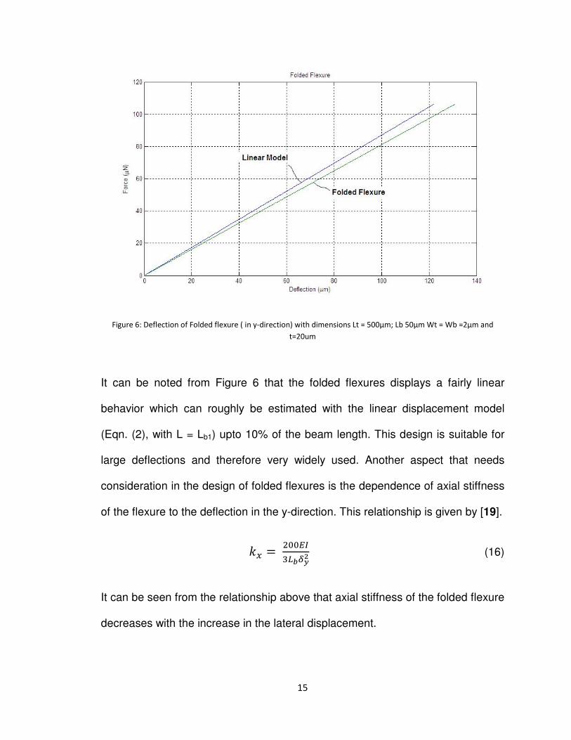
Figure 6: Deflection of Folded flexure ( in y-direction) with dimensions Lt = 500µm; Lb 50µm Wt = Wb =2µm and
t=20um
It can be noted from Figure 6 that the folded flexures displays a fairly linear
behavior which can roughly be estimated with the linear displacement model
(Eqn. (2), with L = Lb1) upto 10% of the beam length. This design is suitable for
large deflections and therefore very widely used. Another aspect that needs
consideration in the design of folded flexures is the dependence of axial stiffness
of the flexure to the deflection in the y-direction. This relationship is given by [19].
OO!CT1 (16)
It can be seen from the relationship above that axial stiffness of the folded flexure
decreases with the increase in the lateral displacement.

16
2.1.4. Serpentine Flexure
The serpentine flexure shown in Figure 7 gets its name from the snake like
pattern of the spring elements. Each meander has a length of ‘a’ and width of ‘b’.
The first and last segments of the meander can be of different length ‘c’ (usually
b/2) or they can be of same length as that of the other segments. Beam
segments that span the meander are called “spans” and the beams that connect
the spans are called connector beams.
Figure 7: Design of Serpentine flexure
Serpentine flexure design offers the advantage of a compliant structure compact
space. The stiffness ratio of the flexure can be adjusted by changing the width of

17
the meander ‘a’. The meandering structure also relieves the residual and
extensional stresses. The formulas for the stiffness of the serpentine flexure are
presented by [41].
For an even number of ‘n’ meanders the stiffness are defined as:
MKCU6!VW Q;XQYV1XU6!VW1 VWQ Q1;XQ6.VW Q;X1 6.Q1 PVWQ VW1;XQ1Y (17)
MKCU6VW Q;X1!QX QYQ1U6!VW1 VWQ Q1;XQ6.VW Q;X1 6.Q1 PVWQ VW1;XQ1Y (18)
For odd number of ‘n’ meanders the stiffness is defined as:
MKCV1XU6VW Q;X1!QX QY (19)
MKCU6VW Q;XQYQ16X;U6!VW1 VWQ Q1;X !VW1Q1Y (20)
Where
F G Z[Q\Z[V
Iza and Izb are the second moment of inertia of the connector and span elements
respectively. Comparison of serpentine flexure to the linear model shown in
Figure 8 below indicates that linear model (Eqn. (2), with L = 500µm) can be
used to estimate the small deflections of serpentine flexure.

18
Figure 8: Deflection of serpentine flexure (in y-direction) with dimensions a = 20µm, b = 20µm, w = 2µm, n = 20 and
t = 20µm
2.2. Electrostatic Force
To simplify the modeling, the electrostatic field between the fixed set of combs
and the compliant set of combs is approximated by one dimensional parallel
plate model between engaged parts of the combs. Therefore the 3D complex
fringing fields, comb finger end effect, ground plane effects and levitation are
neglected for simplicity [45]. This simplification results in the underestimation of
lateral electrostatic force by about 5% [19]. The Capacitance between the comb
fingers in configuration shown in figure 9 is:
] X^_@6`_ `;a (21)

19
Where ‘n’ is the number of combs, ‘ε0’ is the dielectric constant, ‘t’ is the height of
the comb fingers, ‘g’ is the gap spacing between the fingers, ‘l0’ and ‘l’ are the
initial overlap and the comb displacement as a result of the application of the
voltage.
The lateral electrostatic force in the y-direction is equal to the negative derivative
of the electrostatic co-energy with respect to displacement in y direction:
b` c+c` d X^_@a d (22)
Note the relationship between force and voltage is nonlinear and that the other
terms are constants. In the case of parallel plate capacitors (another less
common method of actuation) not only is the force nonlinear with respect to the
applied voltage, but also with the gap (g) between the opposing electrodes. This
is the main reason for the popularity of the comb capacitor configuration.
Figure 9: Schematic details of comb fingers.

20
This electrostatic force produced as a result of the application voltage causes the
movement of the compliant set of comb structure to move in the lateral (y-
direction). This deflection given by:
e X^_@fTa d (23)
2.2.1. Side (Axial) Instability
When the voltage is applied across the opposing comb structures, besides the
electrostatic forces along y-direction electrostatic force is also produced in the x-
direction. This axial electrostatic force tends pull the fingers together. The
electrostatic force generated by both side of the parallel plate capacitor assuming
‘g’ displacement in x-direction is given as:
X^_@6`_ `;6a;1 d X^_@6`_ `;6a ;1 d (24)
Hirano [24] showed that a critical spring constant when the side instability occurs
and fingers stick together is stated as:
hi jcklc mnO X^_@6`_ `;a d (25)
As long as || p qgrsq , instability would not occur. Both the terms are
independently controlled. is determined by the flexure design and hi is

21
determined by the overlap length, finger gap, and the applied voltage. Therefore
the maximum applied voltage bias and hence the allowable maximum deflection
is limited by the side instability.
2.2.2. Front (Lateral) Instability
In addition to the side instability, sometimes the front instability causes the
fingers stick at the front end. This occurs because there is also an electrostatic
force at the front end of the finger. A rough estimation of this force is given by:
t X^_@Q6u`;1 d (26)
Where ‘d’ is the distance from the front end of the moving finger to the base of
the stationary finger, ‘ b’ is the finger width. ‘v’ is the displacement of the finger in
y-direction when no actuation occurs. For an actuator to be in equilibrium the
total electrostatic force produced should then be equal to the restoring force of
the flexure’s spring(s).
w b` t (27)
Also the change in the spring force has to be greater than the electrostatic force
at the front end [21].
ckxc` y ckzc` (28)
By eqns. (26) and (27) maximum allowable displacement gVof the actuator
system can be calculated. The equation of gV is usually a third order

22
polynomial with finger width ‘b’, finger gap ‘g’ and the initial distance ‘d’ as the
variables.

23
Chapter 3
3. DESIGN AND FABRICATION
3.1. Design specifications
To design a MEMS comb drive actuator capable of material testing in-situ in a
TEM, it is important that its design specifications are identified. In order to do so
we assume a specimen made of gold. Gold is very widely used in MEMS devices
as its chemical inertness and resistance to oxidation makes it preferable over
Aluminum. At the macro scale, the most commonly used test for the
determination of the material properties is subjecting of the standard dog-boned
shaped specimens to tensile test. Similar method can be utilized for the material
testing at the micro scale however the cross section of the specimen is changed
from being circular to square for the ease of fabrication using the standard
MEMS fabrication techniques. The equipment at Manufacturing Training and
Technology Center (MTTC) clean room at the University of New Mexico limits the
minimum line width that could be fabricated to 1µm. therefore the sample is
assumed to have the width of 1µm - 2 µm. The thin film thicknesses of interest
for most research groups range between 50nm to 500nm (the upper limit has
been exaggerated in order to overdesign the actuator). 450µm was deemed an
appropriate length for the specimen.
Once the dimensions and the material for the specimen to be tested are specified
the specifications for the actuator are very easily determined. We assume the
maximum displacement that the actuator would have to displace is 10µm. If 0.1%

24
strain to the specimen is required for the study and since the Young’s modulus of
gold is 78GPa then strain is related to the elastic modulus as:
& | (29)
Where the engineering stress ‘σ’ is defined as the force (F) per unit cross
sectional area (A) of the specimen
~ k (30)
Therefore, for a specimen of cross sectional area 2µmx500nm, the actuator
should be capable of producing approximately 78µN of force in addition to the
force required to overcome the restoring force of the spring flexure.
In order to avoid arcing between the opposing comb fingers or between the
comb and the substrate the required force should be generated at low voltage
say ~40 Volts. This electrical breakdown voltage of air depends on the geometry
of the electrode gap, the gas and the pressure in the gap. A generalized
relationship for this breakdown voltage is given by “Paschen’s Law”. The value of
40 Volts is based on this author’s prior experience with MEMS devices of similar
geometry and physical dimensions.
The design of the MEMS comb drive actuator should also accommodate features
that can be used for the calibration. Also the overall size of the device is such
that it can fit into a TEM Holder for JEOL 2010 with the position of the specimen
in the right place in order to conduct in-situ studies. There is also a need to etch
25
a through window in the substrate such as to allow the electron beam to pass
through the specimen to be studied unhindered on to the TEM observation
camera below. As mentioned earlier in Chapter 1 it is also required that the
fabrication of the actuator and the specimen to be tested is to be done separately
which provides more flexibility to the over-all design of in terms of the type of the
specimen that can be tested by ensuring that the fabrication procedure of the
specimen is not restricted by that of the actuator. Due to restriction of minimum
resolvable line width by the available equipment it was concluded that the comb
fingers on the actuator will be 2 µm wide and there will be 2 µm spacing between
them. 10 µm overlap of the opposite fingers was considered sufficient. A vernier
was also accommodated in the design so that the displacement of the compliant
structure can be measured optically.
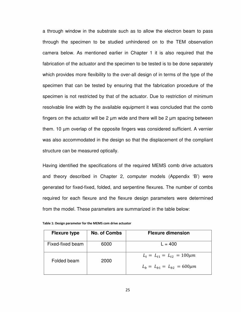
Having identified the specifications of the required MEMS comb drive actuators
and theory described in Chapter 2, computer models (Appendix ‘B’) were
generated for fixed-fixed, folded, and serpentine flexures. The number of combs
required for each flexure and the flexure design parameters were determined
from the model. These parameters are summarized in the table below:
Table 1: Design parameter for the MEMS com drive actuator
Flexure type No. of Combs Flexure dimension
Fixed-fixed beam 6000 L = 400
Folded beam 2000 '@ '@ '@ 100
'Q 'Q 'Q 600

26
Serpentine beam 600
\ 20; ;
r V ; 20
A schematic of the proposed design with fixed- fixed flexure is shown in figure
10 and 11 below:
Figure 10: Schematic design of a Comb Drive Actuator with fixed-fixed flexure
As shown in figure 10 the device consists of a two sets of inter-digitated fingered
structures, one set of fingers connected to the free standing backbone is
anchored to the substrate via flexure (fixed in the figure above) making the
complete structure complaint. Other set of the fingers is rigidly connected to the
substrate.

27
.
Figure 11: Schematic of a custom specimen holder for JEOL 2010 and the placement of the MEMS device
Figure 11 shows a schematic of a custom fabricated specimen holder for JEOL
2010 TEM with feed-thru wires to power and retrieve data from the MEMS device
while under observation in TEM. The detailed manufacturing drawings for this
custom TEM holder are included to this thesis as Appendix ‘C’. Figure 12 below
shows the actual TEM holder.
Figure 12: Custom manufactured TEM holder

28
3.2. Fabrication
3.2.1. Mask Design and Development
The first step in development and fabrication of a MEMS device is the design and
development of photolithography masks. The mask is flat glass plate with the
desires pattern usually of chrome. The mask is required to transfer the required
pattern onto the light sensitive photoresist. The chrome pattern blocks the light
exposure on the part of the wafer coated with photoresist underneath. Making
parts of the photoresist soluble in the developer solution, thereby transferring
pattern.
The mask was designed using the AutoCAD software and all the design
considerations described above were accommodated in the design. As the
MTTC cleanroom facility is equipped for 6 inch wafers the masks designed were
all 7”x7” suitable for 6” wafers. Three masks were designed 1) The basic actuator
pattern, 2) Specimen cavity pattern and 3) A pattern to etch through the wafer to
let the Electron beams pass through a requirement for the TEM analysis. After
the completion of the design the CAD files were sent out to photomask
manufacturer for fabrication.
3.2.2. Actuator Fabrication
The fabrication of the MEMS actuator was carried on Silicon on Insulator (SOI)
wafer whose device layer was 20 µm, buried oxide (BOX) 1 µm and the handle
layer was 600 µm thick. All crystal orientations were (100) and both device and
handle layers were p-type doped with boron. The resistivity of the device layer

29
was 0.01 - 0.02 Ω–cm and >10 Ω–cm for the handle layer. The actuator structure
was then patterned using a layer of photoresist (PR). The device layer was then
etched to the BOX layer by deep reactive ion etching (DRIE) of Si, using the
Bosch [46] Process. This process creates high aspect ratio structures by etching
vertically down from the edge of the PR layer. Next, the PR layer is removed
using acetone, isopropyl alcohol, and de-ionized water rinses respectively.
Finally, an O2 plasma is used to remove any small remaining amount of PR on
the Si surface. Next, the specimen etch structure is patterned on to the wafer by
using a thick photoresist and device layer is again etched 10 µm deep to form a
specimen cavity. Later, the through etch is patterned on the handle layer and the
handle layer is etched all the way to the BOX layer. The photoresist is then
stripped in photoresist stripper. Finally the free standing structure on the actuator
is released by etching the BOX layer in HF bath. For the detailed process
parameters please see Appendix ‘A’. A schematic of the fabrication process is
shown in Figure 13. The actual images of the fabricated devices are shown in
Figure 14-16.

30
Figure 13: A schematic showing the fabrication process of the MEMS actuator

31
Figure 14: Optical micrograph of the actuator with fixed-fixed flexure, L=800, n=600
Figure 15: Optical micrograph of the actuator with serpentine flexure and n=600

32
Figure 16: Optical micrograph of the actuator with Folded flexure and n=2000

33
Chapter 4
4. TESTING AND CALIBRATION
This chapter describes the setup and the procedure employed for testing and
calibrating the fabricated MEMS actuators.
4.1. Side Instability Voltage
The determination of the side instability voltage is important because the
instability voltage limits the amount of force that can be generated by the comb
fingers before they stick to each other and electrically short out the device. This
determination of the side instability voltage and hence the maximum force that
the device can be used to apply is a major factor in determining the application
for which a particular device can be used.
4.1.1. Setup
The testing for the side instability voltage of the MEMS actuator was done on a
Probe-station. The wafer was placed on the probe station stage and held with
the vacuum. The probe tips were brought in contact with the bonding pads on the
device. The probe station tips were connected to the Agilent E3612A power
supply to operate the device. The probe station microscope was used to observe
the device while in operation. The complete setup is shown in the Figure 17 and
18 below:

34
Figure 17: Experimental setup used to determine the side instability
Figure 18: Probe tips in contact with bonding pads of a MEMS actuator

35
4.1.2. Procedure
In order to determine the side instability voltage of the MEMS actuator positive
bias was applied to the fixed structure and while compliant structure was
grounded. The substrate (handle layer of the wafer) was also grounded by
grounding the probe station stage. The voltage was increased in the increments
of 1V and the combs on the actuator were observed through the microscope. The
voltage at which the opposite comb fingers start to come closer to each other
laterally is the side instability voltage. The laterally movement of the comb fingers
can be observed through the microscope and corresponding voltage is noted.
4.2. Calibration
Measurement of small forces (fN to nN) are the cause of numerous scientific
breakthroughs in the last few decades. The vast majority of force measurements
made below a µN are for the purpose of determining material properties.
Examples are: measurement of single ligand-receptor interactions (~fN–pN)
using the Surface Force Apparatus (SFA) [47,48], measurement of the
mechanical properties of nanostructures (nN–mN) using Nano /
Microelectromechanical Systems (NEMS/MEMS) [49,38,43], and a plethora of
measurements have been made on the range of pN to nN using the Atomic
Force Microscope (AFM). These measurements are becoming increasingly
common, yet there is no traceable method of calibrating this full range of forces
[50]
The NanoManufacturing Industry is not prepared for mass production of products
utilizing nanotechnology. Scientists are constantly synthesizing and fabricating

36
novel nanomaterials and nanodevices (NEMS). Clearly transitioning these
NanoScience discoveries into the NanoManufacturing realm would allow society
to reap the reward of decades of scientific work. Yet NanoManufacturing of such
products requires a nanometrology infrastructure that is lacking in many
respects. Nanometrology is a term that, currently, implies measurements at the
nanoscale and below. As such force metrology at sub-nN scales is considered to
be a part of the nanometrology world.
Why is nanometrology important? Materials with dimensions on the nanoscale
can have drastically different properties from their bulk counterparts. For
example, bulk gold is a noble metal, i.e. it is inert. Yet nanoparticles (~2 nm) of
gold have a high chemical reactivity and are employed as catalysts. Similarly,
shrinking down to the nanoscale changes the density of electronic states of a
material giving to different electrical and optical properties and it also affects the
mechanical properties of the material [51].
Traceable force calibrations are necessary to allow for the measurement of the
mechanical properties of materials. More specifically, it is essential that
measurements of mechanical properties be made using standardized methods
with International System of Units (SI) traceable equipment. Without
standardized testing methods and SI traceable equipment, bridges and building
would fall and pressure vessels would explode as a result of improper design.
As an example of this necessity, consider the elastic modulus of steel. Using
standard testing methodologies (ASTM E 111) and SI traceable equipment we
know that the elastic modulus of steel is typically 200 GPa. This value is

37
repeatable all over the world and is of extreme importance to Mechanical and
Civil Engineers alike.
Next consider the elastic modulus of gold, an element that is particularly
important to the semiconductor industry. The bulk value, measured using
standard methods and SI traceable equipment is 77 GPa [52], whereas samples
with cross-sectional dimensions under 1 micron have values that vary
considerably. For example, Wu et al. report values for elastic moduli of gold
between 45 and 107 GPa [53], while Espinosa reports that Egold is “consistently”
between 53-55 GPa [54], and Leseman et al. found that the Egold was 76 GPa
[49].
Are all these researchers correct? It may be that all measurements were correct,
but in order to remove all doubt use of standard testing methods and SI traceable
equipment should be undertaken. Again, shrinking dimensions to the nanoscale
will change the behavior of materials and systems, thus establishing standard
testing methods and utilizing SI traceable equipment with proper force resolution
is necessary. Because of the vast number of different methodologies of material
growth, and geometries to which they conform, it will be some time before
standard testing methodologies are developed for every material type and
geometry. Therefore, because of the ingenuitive growth methods for materials, it
can only be asked that researchers’ equipment be SI traceable and not force
them to conform to standard testing methodologies. This is the more realistic and
attainable short-term goal. Therefore all the MEMS devices fabricated for this

38
study were calibrated by employing a recently developed method traceable to
NIST standards [39].
4.2.1. Setup
The calibration setup consists of two components, the MEMS actuator mount and
the alignment setup. The actuator mount is prepared by cleaving the substrate
just below the lamp-shade shaped feature on the actuator. The actuator is then
carefully adhered to a glass microscope slide using double sided adhesive tape.
In order to measure the capacitance change between the comb figures
wirebonds are made from the bonding pads on the actuator to the copper tape on
the glass (Figure 19). The leads from the Agilent 4980A precision LCR meter
were later connected to the mounted actuator.
Figure 19: MEMS actuator mounted on the glass slide
The alignment setup consists of set of precision linear translation stages and a
goniometer (Figure 20-22).

39
Figure 20: Glass slide mounted on the goniometer and independent linear stage for movement in z-direction
Figure 21: Microscope mounted on separate linear stages for independent x-y-z movement

40
The actuator was mounted onto a fixture that translates in the z-direction with a
goniometer that allow for rotation around the x-axis. The alignment of ball lenses
was carried out by mounting them on another set of x–y linear translation stages.
A tube microscope with a CCD camera was also mounted on a separate set x-y-
z linear translation stages for the ease of observation. An observation
microscope with a CCD camera is mounted on separate x-y-z stages which
makes it independent from the rest of the setup. The complete setup is shown in
Figure 22 below:
Figure 22: The complete calibration setup

41
4.2.2. Procedure
Calibration of the actuators is accomplished by recently developed calibration
technique [55,39]. In order to calibrate known weights are hung from the portion
of the actuator that extends beyond the cleave line of the wafer. After hanging
the weight the change in capacitance between the comb fingers is measured with
the LCR meter. Capacitance measurement provides very accurate displacement
measurements with a tolerance of +100nm. Hanging the weights, not
surprisingly, requires extreme care. The weight is first properly aligned to the
load cell using linear translation stages and goniometer. Weights were adhered
to the load cell by using ‘‘secondary forces’’ and adhesives.
The calibration weights are commercially available sapphire ball lenses. These
ball lenses are manufactured to tight specifications that allow great confidence in
the weight of each sphere. The manufacturer’s specification for density, q, is 3.98
± 0.01 g/cm3. Tolerances on all diameters was ±2.54µm. Independent
verification was performed on several samples, through the use of a precision
balance that is traceable to the National Institute of Standards and Technology
(NIST), and it was found that all samples tested fall within the manufacturer’s
specifications.
To attain a centrally loaded structure, proper alignment between the actuator and
the ball lenses is necessary. This was accomplished through the use of three
linear translation stages and a goniometer (Figure 19). The actuator was
mounted onto a fixture that translates in the z-direction with goniometer that allow
for rotation around the x-axis (axis perpendicular to the plane of the die). The ball

42
lenses were mounted onto a custom stage that allowed for the rigid temporary
attachment of the ball lens to the x–y linear translation stages. Upon proper
alignment of the actuator and ball lens to gravity the ball lens was adhered to the
load cell.
A non-linear force–displacement response for the fixed-fixed beam structure was
anticipated, thus a range of weights was hung from each load cell to capture the
load cell’s non-linear response. For ball lenses measuring, 300 and 500 µm in
diameter, it was possible, when the humidity was relatively low, to attach the
balls using static electricity. When the humidity was relatively high, it was
possible to attach the balls using water menisci formed by the condensed water
from the humidity. Figure 23 shows an optical micrograph of a 790 µm sapphire
ball lens attached in this manner to the load cell.
Figure 23: Optical micrograph of 790 µm sapphire sphere attached to the actuator

43
Images of spheres attached by static electricity are similar. Detachment of these
smaller spheres was possible through the use of surface tension. A droplet of
water was placed onto a substrate and the sphere was brought near. When the
sphere was placed into contact with the water, the water quickly pulled the ball
from the actuator without damage.
At the extreme end of our load range the large diameter spheres (1000 µm, 1500
µm) were attached using photoresist as an adhesive. These spheres were
attached by dipping the load cell’s tip into a droplet of photoresist (Figure 24).
The photoresist wicked into the load cell’s specially designed ‘lamp-shade’ tip,
this ‘wet’ tip was then lowered into contact with a large diameter sapphire sphere.
Solvents quickly escape the small volume of resist needed to adhere the ball lens
to the load cell, especially under the intense light of the microscope. It was
possible to detach the spheres by vibrating the load cell. This was done at some
risk though, as some devices were damaged in this process. An alternate
method of removal of the ball lens and photoresist was performed by placing a
dish of acetone under the load cell and ball lens assembly. The acetone vapor
quickly weakens the positive photoresist because of the large dose of light it has
received from the focused light of the microscope. Submersion of the ball lens
and device was not necessary for ball lens removal.

44
Figure 24: Actuator tip dipped in photoresist droplet
It should be noted at this point that the weight of the member from which the
weights hang and the liquids used for attachment never total to greater than
0.1% of the minimum weight hung from the load cell. Therefore, this additional
weight can be safely neglected.

45
Chapter 5
5. EXPERIMENTAL RESULTS AND DISCUSSION
5.1. Compressive Residual Forces
After the fabrication was completed, physical inspection of the wafer was
conducted under the optical microscope. Buckling was observed on almost all of
the flexure beams. It is believed that this buckling is due to the compressive
residual forces. These residual forces could not have been induced during the
device fabrication due to lack of high temperature processing. These forces are
believed to be intrinsic to the wafer itself, induced, during its production perhaps
during the oxide growth or bonding with the handle layer.
In order to quantify the buckling several strain gauges were purposefully
designed on the masks. It was observed that these compressive residual forces
vary from location to location on the wafer and hence buckling on the beams
depended on the location of the device on the wafer. These strain gauges
consisted of fixed-fixed beams of various lengths with a vernier at the center, the
point that would be point of inflection after the buckling. It was observed that the
deflection on 800µm beam (the same length as that on the fixed flexure) was
approx 1.5µm near the edges of the wafer and approx 5µm at the centre of the
wafer. Figure 25 below shows the buckled strain gauges at the center of the
wafer. In an unbuckled beam both the verniers would have been aligned, the fact
they are not means that the residual stress in the wafer increased the critical
stress value for the beams and caused buckling. The displacement at the center
of the beam is related to the compression by Saif et. al. in [43].

46
Figure 25: Optical micrograph of the strain guage at the centre of the wafer
These residual stresses were not accounted for in any of the models and with the
beams buckled the actual response is different from what is expected. It was
observed that the devices with fixed-fixed flexure and folded flexure were still
usable but the effect of compressive residual stresses on the devices with the
serpentine flexure was so large that it had rendered the devices unusable.
5.2. Side Instability Voltage
The parameter that is most affected by the existence of the residual forces and
buckling is the side instability voltage. The presence of uneven compressive
residual forces and the buckled beams generates moments which brings the side

47
instability voltage down from hundreds of volts to on the order of 10 volts in most
cases. The observed value of side instability voltage on the actuators with fixed-
fixed flexures is 15-18V, while for the actuators with folded flexure is 5-7V. As the
side instability voltage depends on the amount of the compressive residual
stresses in the wafer it varies for each kind of actuator depending upon its
location on the wafer. This low side instability voltage severely affects the
maximum force that can be applied and the maximum allowable comb
displacement of the MEMS actuators.
5.3. Calibration
There are number of factors that can affect the response of the actuators. The
first source of uncertainty is the dimensional uncertainty. The designed values of
the spring and comb finger widths and on the mask is 2 +/-0.2µm, assuming that
photolithographic process was meticulously fine tuned and dimensions
transferred on the wafer are exactly the same as that on the mask (not the actual
case of course!) then the width of the springs in the flexure can be anywhere
between 1.8 - 2.2µm. Similarly the comb finger gap can be anything between 1.6
- 2.4µm. The wafer tolerance on the handle layer thickness was 20 +/- 0.5 µm,
which means that the height of the structure after it has been released could vary
between 19.5 - 20.5 µm.
The second source of uncertainty is the uncertainty in the material properties of
the silicon. The value for the Young’s Modulus for the Single Crystal Silicon
(SCS) varies between 62 - 179 GPa [56]. The elastic modulus depends on the
crystal orientation and type and amount of doping. The moduli expected for these

48
devices, which correspond to 110 plane varies between 150-170 GPa [57].
These variations in dimensions and physical properties of the silicon lead to
uncertainty in the actual response of the actuator.
A general method to deal with the propagation of uncertainties is given by [58].
Suppose if ‘R’ is function of variable g, v and with uncertainties:
6g, v, ; (31)
Then the uncertainty in ‘R’ due to g alone would be:
∆ 6g ∆g, v, ; 6g, v, ; (32)
Where ∆g is the uncertainty in g, similarly the uncertainty in ‘R due to v and will
be:
∆ 6g, v ∆v, ; 6g, v, ; (33)
∆[ 6g, v, ∆; 6g, v, ; (34)
Therefore the net uncertainty is calculated as a square root of the sum of
squares of the individual contributions:
∆ 6∆; 6∆; 6∆[; (35)
The formal justification for this statement comes from the theory of statistical
distributions and assumes that the distribution of successive variable values is
described by the so-called Gaussian distribution. Note that this general method

49
applies no matter what functional relationship between R and the various
variables. It is not restricted to additive and multiplicative relationship as are the
usual simple rules for handling uncertainties.
The above uncertainty analysis can be used to calculate the uncertainty in the
device response due to the variation in the physical dimensions and material
properties of the MEMS device. But there is a third and unpredictable source of
uncertainty, the residual stresses in the wafer. These residual stresses induce
residual forces in the device and make the response from each device unique.
Modeling these residual stresses also presents a challenge. And even if they are
accurately modeled, the combined uncertainty of all the three sources of variation
will be very large making the accurate prediction of the actuator response
impossible.
In order to eliminate this huge uncertainty in the calculated response each MEMS
device can be individually calibrated by the method described in the previous
chapter. It not only gives a very accurate response (very small uncertainty) for
the device but also the calibration method can be traced back to the NIST
standards ensuring that the results from different experiments can be compared.
5.3.1. Fixed-fixed flexure
A MEMS actuator with fixed-fixed flexure was calibrated using the method
described in the previous chapter. Force vs. Capacitance change was noted.
Later, the same device was measured in a SEM. Using the measured

50
dimensions the capacitive measurements were transformed to the equivalent
displacement using equation (21).
] X^_@6`_ `;a (21)
Figure 26 gives Force versus displacement curve for the calibrated fixed-fixed
flexure.
Figure 26: Calibration curve for the fixed-fixed flexure
Curve fit equation and value for the calibrated device is:
0.4385g! 0.3024 g 0.2272
0.9997

51
The error bars on the displacement (x-axis) are due to the measurement
uncertainty and are equal to +/- 100nm. The uncertainty on the force (y-axis) is
very small to display on the chart above. Table below gives the uncertainty on
force for each diameter sphere. This uncertainty is due to the manufacturing
tolerance of +/-2.542µm on the diameter of the sphere.
Sphere Diameter
(µm)
Force (µN)
Force Uncertainty
(µN)
790 10.07 +/- 0.09uN
1000 20.42 +/- 0.15uN
1500 6.8.92 +/- 0.35uN
1580 80.55 +/- 0.38uN
Figure 27 shows the uncertainty in the response of the actuator due to the
dimensional variations for elastic modulus of 150GPa and 170GPa. The
uncertainty increases with higher modulus.

52
Figure 27: Range of uncertainty in actuator response with elastic modulus 150 – 170 GPa
Comparison between the calibrated response of the MEMS actuator and the
modeled uncertainty is shown in Figure 28.
Figure 28: Comparison between the calibrated response and the uncertainty due to dimensional variation of device
with fixed-fixed flexure
0
10
20
30
40
50
60
70
80
90
100
0 2 4 6 8
Fo
rce
(uN
)
Displacement (um)
Comparision between the calibrated response and
the uncertainaty due to dimensional variation

53
It can be seen on the curves above that there exist an uncertainty of 1-2µm at
large deflections. Also despite the residual stresses on the wafer the response of
the MEMS actuator closely follows the predicted curves for very small
deflections. Making this type of the actuator ideal for testing metals where
maximum required elongation is less than 0.5 µm.
5.3.2. Folded flexure
A MEMS actuator with folded flexure was also calibrated and the analysis similar
to the one described in the section above was performed. Figure 29 gives Force
versus displacement curve for the calibrated folded flexure.
Figure 29: Calibration curve for the folded flexure
Curve fit equation and value for the calibrated device is:
0.8198 g 0.0033

54
0.9993
The error bars on the displacement (x-axis) are due to the measurement
uncertainty and are equal to +/- 100nm. The uncertainty on the force (y-axis) is
very small to display on the chart above. Table below gives the uncertainty on
force for each diameter sphere. This uncertainty is due to the manufacturing
tolerance of +/-2.542µm on the diameter of the sphere.
Sphere Diameter
(µm)
Force (µN)
Force Uncertainty
(µN) 300 0.55 +/- 0.01uN
500 2.55 +/- 0.04uN
790 10.07 +/- 0.09uN
Figure 30: Range of uncertainty in actuator response with elastic modulus 150 – 170 GPa

55
Comparison between the calibrated response of the MEMS actuator and the
modeled uncertainty is shown in Figure 31.
Figure 31: Comparison between the calibrated response and the uncertainty due to dimensional variation of device
with folded flexure
It can be seen on the curves above that there exist a huge uncertainty at all
deflections. Therefore use of this type of flexure for any kind of testing would give
misleading results unless the actuator is calibrated and its response is noted and
accounted for prior to testing. This kind of flexure can be used for applications
with very large deflections thus making it a good candidate for testing polymers
or biological materials.
-2
0
2
4
6
8
10
12
0 5 10 15 20 25
Fo
rce
(uN
)
Displacement (um)
Comparision between the calibrated response
and the uncertainaty due to dimensional
variation

56
Chapter 6
6. CONCLUSION
This thesis gives the detailed account of the design process employed to design,
fabricate and calibrate MEMS comb drive actuators that could be used for in-situ
materials testing. Since this actuator is processed separately from the test
specimen therefore, the processing of the specimen is not dependent on the
actuator itself. The reasons have been discussed which make the actual
response of the MEMS devices deviate from the modeled response. The
presence of residual stresses on the wafer makes the behavior of each device
unique. The unique behavior of these devices necessitates their calibration
before they could be used for material testing. Three different flexure designs the
fixed-fixed, folded and serpentine flexure were fabricated for the purpose of this
study. Of the three, the compressive residual stresses on the wafer rendered the
devices with the serpentine flexure unusable. A recently developed method of
calibration that can be traced back to the NIST standards was employed to
calibrate the devices with fixed-fixed and folded flexures [39]. Their actual
behavior was compared to their modeled behavior. It has been shown devices
with the fixed-fixed flexure can be used for testing materials that do not require
large elongation like metals even without calibration. The devices with folded
flexure can be used to test the materials that require large elongation like
polymers and biological cells. But these devices must be calibrated and their
force versus displacement curves must be determined before using them as
actuators for materials testing.

57
6.1. Future Work
The devices have very low side instability voltage. Further study is required to
investigate methods through which the devices could be made to operate on
voltages up to 40 Volts. Further investigations are also required on methods to
measure the capacitance change across the comb finger while a DC is bias is
applied across them to actuate the device.

58
Bibliography
[1] K. E. Petersen, "Silicon as a mechanical material," in Proceedings of the IEEE, vol.
70, May 1982, pp. 420-457.
[2] R. S. Muller, "From IC's to microstructure: materials and technologies," in IEEE
Micro Robots and Teleoperators Workshop, Hyannis, Mass., Nov. 9-11, 1987.
[3] M. Mehregany, K. J. Gabriel, and W. S. N. Trimmer, "Integrated fabrication of
polysilicon fabrication," IEEE Trans. Electron Devices, vol. ED-35, pp. 719-723,
1988.
[4] T. A. Lober and R. T. Howe, "Surface micromachining processes for electrostatic
microactuator fabrication," in Technical digest, IEEE Solid-State snsors and
Actuators Workshop, Hilton Head Island, SC., June 1988, pp. 59-62.
[5] J. A. Schweitz, K. Hijrot, and B. Hok, "Bulk and surface micromachining of GaAs
structures," in Technical Digest, IEEE Micro Elctro Mechanical Systems Workshop,
Napa Valley, CA, Feb. 1990, pp. 73-76.
[6] M. J. Madou, Fundamentals of Microfabrication: the science of miniturization, 2nd
ed.. Washington, D.C., US: CRC Press LLC, 2002.
[7] M. T. A. Saif and N. C. MacDonald, "A millinewton microloading device," Sensors
and Actuators A, vol. 53, pp. 65-75, 1996.
[8] A. Jazairy and N. C. MacDolnald, "Planar Very High Aspect Ratio
Microstructuresfor Large Loading Forces," Microelectronic Engineering, vol. 30,
pp. 527-530, 1996.
[9] D. Hah, P. R. Patterson, H. D. Nguyen, H. Toshiyoshi, and M. C. Wu, "Theory and
Experiments of Angular Verticle Comb Drive Actuators for Scanning Micrmirrors,"
Journal of selected topics in Quantum Electronics, vol. 10, no. 3, pp. 505-513, May
2004.
[10] C. S. B. Lee, S. Han, and N. C. MacDonald, "Single Crystal Silicon (SCS) XY-Stage
Fabricated by DRIE and IR Allignment," in The 13th Annual International
Conference on Micro Electro Mechanical Systems, Miyazaki, Japan, Jan 2000, pp.
28-33.
[11] M. Suster, J. Guo, N. Chaimanonart, W. H. Ko, and D. J. Young, "High Performance
MEMS Capacitive Strain sensing System," Journal of Microelectromechanical
Systems, vol. 15, no. 5, pp. 1069-1077, Oct. 2006.
[12] W. C. Tang, T. H. Nguyen, and R. T. Howe, "Laterally Driven Polysilicon Resonant
Micrstructures," Sensors and Actuators, vol. 20, pp. 25-32, 1989.
[13] W. C. Tang, "Electrostatic Comb Drive for Resonant Sensor and Actuator
Applications," PhD Dissertation, Faculty of Electrical Engineering and Computer
Sciences, University of California, Berkeley, CA, 1990.
[14] S. P. Pacheco, L. P. B. Katehi, and C. T. Nguyen, "Design of Low Actuation
Voltage RF MEMS Switch," in IEEE MTT-S International Microwave Symposium,

59
Boston, MA, 2000 , pp. 165-168.
[15] S. Renard, C. Pisella, J. Collet, V. Gaff, and J. .-L. Lauront, "Capacitive pressure and
Intertial Sensor by Epi-SOI Surface," in Proceedings of IEEE Sensors, 2002, pp.
1385-1388.
[16] M. Esashi, S. Shoji, and A. Nakano, "Normally Close Microvalve and Micropump
fabricated on Silicon Wafer," in Technical Digest, IEEE Microelectromechanical
Systems Workshop, Salt Lake City, UT, Feb 1989, pp. 29-34.
[17] H. Jerman, "Electrically Activated Micromachined diaphragm valves," in Technical
Digest, IEEE Solid State Sensors and Actuators Workshop, Hilton Head Island, SC.,
Jun 1990, pp. 65-69.
[18] M. A. Huff, M. S. Mettner, T. A. Lober, and M. A. Schmidt, "A Pressure Balanced
Electrostatically Actuated Microvalve," in Technical Digest, IEEE Solid State
Sensors and Actuators Workshop, Hilton Head Island, SC., Jun 1990, pp. 123-127.
[19] R. Legtenberg, A. W. Groeneveld, and M. Elwenspoek, "Comb Drive Actuators for
Large Displacements," J. Micromech. Microeng, vol. 6, p. 320–329, Jun. 1996.
[20] Y. H. Cho and P. A. Pisano, "Optimum Structural Design of Micrmechanical Crab-
Leg Flexures with microfabrication constraints," in Proceedings of ASME Winter
Annual Meeting, DSC 19, 1990, pp. 31-49.
[21] V. P. Jaecklin, C. Linder, N. F. de Rooij, and J. M. Moret, "Micromechanical comb
actuators with low driving voltage," J. Micrmech. Microeng., vol. 2, pp. 250-255,
1992.
[22] W. Ye, S. Mukherjee, and N. C. MacDonald, "Optimal Shape Design of an Electric
Comb Drive in Microelectromechanical Systems," Journal of
Microelectromechanical Systems, vol. 7, no. 1, pp. 16-26, Mar. 1998.
[23] J. D. Grade, H. Jerman, and T. W. Kenny, "Design of Large Deflection Electrostatic
Actuators," Journal of Micrelectromechanical Systems, vol. 12, no. 3, pp. 335-343,
Jun. 2003.
[24] T. Hirano, T. Furuhata, and K. J. Gabriel, "Design, fabrication and operation of
submicron gap comb-drive microactuators," J. Microelectromech. Syst., vol. 1, no. 1,
pp. 52-59, 1992.
[25] A. P. Pisano and Y. H. Cho, "Mechanical design issues in laterally driven
microstructures," Sensors and Actuators A: Physical, vol. 23, no. 1-3, pp. 1060-
1064, Apr. 1990.
[26] M. T. A. Saif and N. C. MacDonald, "Design Considerations for Large MEMS," in
Proceedings of SPIE, Vol 2448, San Deigo, CA, 1995, pp. 93-104.
[27] M. T. A. Saif and N. C. MacDonald, "Planarity of Large MEMS," Journal of
Microelectromechanical Systems, vol. 5, no. 2, pp. 79-97, Jun. 1996.
[28] J. J. Sniegowski and C. Smith, "An Application of Mechanical Leverage to
Microactuation," in Proceedings of TRANSDUCERS'95 EUROSENSORS IX,
Stockholm, Sweden, June 1995, pp. 364-367.
[29] W. A. Moussa, H. Ahmad, W. Badawy, and M. Moussa, "Investigating the
Reliability of Electrostatic Comb-Drive Actuators Utilized in Microfluidic and
Space systems Using Finite Element Analysis," Canadian Journal of Electrical and

60
Computer Engineering, vol. 27, no. 4, pp. 195-200, Oct. 2002.
[30] S. Krylov, N. Moussay, and Y. Bernstein, "Sensitivity Study of Comb-drive
Actuator with Folded Suspension," in Proceedings of 11th International Conference
on Fracture, Turin, Italy, Mar 2005.
[31] H. Huang and F. Spaepen, "Tensile testing of free standing Cu, Ag and Al thin films
and Ag/Cu multilayers," Acta Materialia, pp. 3261-3269, 2000.
[32] A. J. Kalkman, A. H. Verbruggen, and C. A. M. Janssen, "Young's modulus
measeurement and grain boundary sliding in free standing thin metal films," Applied
Physics Letters, vol. 78, pp. 2673-2675, 2001.
[33] R. J. Vinci and J. J. Vlassak, "Mechanical behaviour of thin films," Annual Review
of Material Science, pp. 431-462, 1996.
[34] U. Landman, W. D. Luedtke, N. A. Burnham, and R. J. Colton, "Atomistic
mechanism and dynamic adhesion, nanoindentation and fracture," Science, New
series, vol. 248, pp. 454-461, 1990.
[35] M. A. Haque and B. A. Samuel, "Room temperature relaxation of free standing
nanocrystaline gold film," Journal of micromechanics and microengineering, vol.
16, pp. 929-934, 2006.
[36] A. Hadrboletz, B. Weiss, and G. Khatibi, "Fatigue and fracture properties of thin
metalic foil," International Journal of Fatigue, vol. 109, no. 1, pp. 68-89, 2001.
[37] Y. Zhu and H. D. Espinosa, "An elecomechanical material testing system for in situ
electron microscopy and applications," Preceedings of National Academy of
Sciences, vol. 102, no. 41, pp. 14503-14508, Oct. 2005.
[38] M. A. Haque and M. T. A. Saif, "Microscale materials testing using MEMS
actuator," Journal of Microelectromechanical Systems, vol. 10, no. 1, pp. 146-152,
2001.
[39] K. Abbas, Z. C. Leseman, and T. J. Mackin, "A novel method for the calibration of
MEMS load cells," International Journal of Mechanics and Materials in Design,
vol. 4, pp. 383-389, Mar. 2008.
[40] W. C. Young, Roark's Formulas for Stress and Strian, 6th ed.. McGraw Hill, 1989.
[41] G. K. Fedder, "Simulation of microelectromechanical systems," PhD. Dissertation,
Faculty of Electrical Engineering and Computer Sciences, University of California,
Berkeley, CA, 1994.
[42] R. Frisch-Fay, Flexible Bars. Ryde, New South wales, Australia: Butterworths &
Co. Limited, 1962.
[43] M. T. A. Saif and N. C. MacDonald, "Measurement of forces and spring constants of
microinstruments," Review of Scientific Instruments, vol. 60, no. 3, pp. 1410-1422,
Mar. 1998.
[44] M. W. Judy, "Micromechanisms using sidewall beams," PhD Dissertation, Faculty
of Electrical and Computer Sciences, University of California, Berkeley, CA, 1994.
[45] W. C. Tang, M. G. Lim, and R. T. Howe, "Electrostatic comb drive levitation and
control method," J. Microelectromech. Syst., vol. 1, pp. 170-178, 1992.
[46] F. Larmer and A. Schilp, "Method for anisotropically etching silicon," Patent
DE4241045, US 5501893, and EP 625285, 1992.

61
[47] J. N. Israelacvili and G. E. Adams, "Direct measurement of long range forces
between two mica surfaces in aqueous KNO3 solutions," Nature (London), vol. 262,
pp. 774-776, 1976.
[48] C. A. Helm, W. Knoll, and J. N. Israelachvili, "Measurement of Ligand-Receptor
Interactions," in Proceedings of the National Academy of Sciences of the United
States of America, vol. 88, 1991, pp. 8169-8173.
[49] Z. C. Leseman and T. J. Mackin, "Determination of the mechanical properties of
freestanding nano-thickness gold membranes using a novel MEMS based load cell,"
Sensors & Actuators A, vol. 134, pp. 264-270, 2007.
[50] J. R. Pratt, D. B. Newell, J. A. Kramar, and E. Whitenton, "Calibration of
piezoresistive cantilever force sensors using the NIST electrostatic force balance," in
Proceedings of the IMECE 2003 ASME International Mechanical Engineering
Congress, Washing D. C., 2003, pp. 289-292.
[51] J. Rajagopalan, J. Han, and M. T. A. Saif, "Plastic Deformation Recovery in
Freestanding Nanocrystalline Aluminum and Gold Thin Films," Science, vol. 315,
pp. 1831-34, 2007.
[52] J. R. Davis, Metals Handbook, 2nd ed.. ASM International, 1998.
[53] B. Wu, A. Heidelberg, and J. J. Boland, "Mechanical properties of ultrahigh-strength
gold nanowires," Nature Materials, 2005.
[54] H. D. Espinosa, B. C. Prorok, and B. Peng, "Plasticity size effects in free-standing
submicron polycrystalline FCC films subjected to pure tension," Journal of the
Mechanics and Physics of Solids, vol. 52, pp. 667-689, 2004.
[55] Z. C. Leseman and T. J. Mackin, "Indentation testing of axisymmetric freestanding
nanofilms using a MEMS load cell ," Sensors and Actuators A: Physical, vol. 134,
no. 1, pp. 264-270, Feb. 2007.
[56] B. Bhushan and X. Li, "Micromechanical and tribological characterization of doped
single crystal silicon and polysilicon films for microelectromechanical systems,"
Journal of Material Research, vol. 12, no. 1, pp. 54-63, Jan. 1997.
[57] J. J. Wortman and R. A. Evans, "Young's modulus, Shear modulus and Poisson's
Ratio in Silicon and Germanium," Journal of Applied Physics, vol. 36, no. 1, pp.
153-156, Jun. 1964.
[58] J. Taylor, An Introduction to Uncertainty Analysis, 2nd ed. Boulder, Colorado: Univ
Science Books, 1996.

62
Appendix ‘A’
A. FABRICATION PROCEDURE
HF Cleaning
Process
Step Tool Program Parameters Comments
BHF
Cleaning Acid Bench
6:1 BOE 60 sec
6 Pts 40% NH4F; 1 Pt 49%
HF Acid
QDR
Caustic
Bench 5 cycles
Spin Rinse
Dryer Verteq Program 1
Resistivity DI water: 15 - 18
mega ohm
Dehydration
Bake Hot Plate 200o C, 5 min
Actuator Pattern
Process
Step Tool Program Parameters Comments
HMDS Spin
CEE
Coater Program 4
500 rpm, 5
sec
5000 rpm, 20
s HMDS single Dispense with
repeater setting 3ml
PR Spin
CEE
Coater Program 4
500 rpm, 5
sec
5000 rpm, 20
s AZ5214 Double Dispense
with repeater setting 10ml
Soft Bake Hot Plate 105o C, 90 s
Expose Karl Suss
Hard
Contact Mask: Actuator, Exp: 6 sec
Intensity: @365nm =
5.8mW/cm2; @405nm =
11.3mW/cm2
Develop
Caustic
Bench 2min AZ400K; 4:1 with slight agitation
QDR
Caustic
Bench 5 cycles
Spin Rinse
Dryer Verteq Program 1
Resistivity DI water: 15 - 18
mega ohm

63
Inspection
Nikon
Microscope
DRIE Etch (Device) & Cleaning
Process
Step Tool Program Parameters Comments
DRIE Etch
Adixen
DRIE
Std 15 Min
Si
1800W,
C4F6, SF6 2-3u/min
Remove PR
Solvent
Bench Acetone, Methano, IPA, N2
PR Stripping Acid Bench 15 min H2SO4+H2O2
QDR
Caustic
Bench 5 cycles
Spin Rinse
Dryer Verteq Program 1
Resistivity DI water: 15 - 18
mega ohm
Descumming
March RIE
Etcher Program 1
152 watt; 60
sec
83% O2 (Gas
4)
Backside Photo Lithography
Process
Step Tool Program Parameters Comments
HMDS Spin
CEE
Coater Program 2 500 rpm, 5 s
1000 rpm, 60
s HMDS single Dispense with
repeater setting 3ml
PR Spin
CEE
Coater Program 2 500 rpm,5 s
1000 rpm, 60
s AZ9260 Triple Dispense
with repeater setting 8ml
Soft Bake Hot Plate 120o C, 2min
Expose Karl Suss
Vacuum
Contact
Mask: Backside Etch, Exp:
300 sec
Intensity: @365nm =
5.8mW/cm2; @405nm =
11.3mW/cm2
Develop
Caustic
Bench 5 min AZ400K; 3:1 With agitation
QDR
Caustic
Bench 5 cycles

64
Spin Rinse
Dryer Verteq Program 1
Resistivity DI water: 15 - 18
mega ohm
Inspection
Nikon
Microscope
DRIE Etch (Backside)
Process Step
Tool Program Parameters Comments
DRIE Etch Adixen DRIE
Std 90 Min Si
1800W, C4F6 (150 sccm, 3 sec), SF6 (300 sccm 7sec)
Pbias (~70W), Valve/pressure (48%/3.8 Pa), He (10mbar),Temp ( 20oC)
DRIE Etch Adixen DRIE
Std 30 Min Si
1500W, C4F6 (320 sccm, 2 sec), SF6 (400 sccm 5sec)
Pbias (90W, 10%-10ms), Valve/pressure (100% / 4 Pa), He (10mBar), Temp (20oC)
Remove PR Solvent Bench
Acetone, Methanol, IPA, N2
PR Stripping Solvent Bench
80o C, 15min EKC 830
QDR Caustic Bench
5 cycles without sprinklers
Hand Drying
Dehydration Bake
Hot Plate 180o C, 5 min
Cool 20 sec
HF Release
Process Step
Tool Program Parameters Comments
BHF release Acid Bench
6:1 BOE 20 mins 6 Pts 40% NH4F; 1 Pt 49% HF Acid
QDR Caustic Bench
5 cycles without sprinklers
Hand Drying

65
Appendix ‘B’
B. MATLAB CODES
%
//---------------------------------------------------------------------
---
Mathematical model for Comb Drive Actuators with Fixed-Fixed beams of rectangular cross sections
-----------------------------------------------------------------------
--//
%
Close all clear all clc
% //--------------Variable Definitions--------------//
n = 600; %No. of teeth OL = 10e-6; %Intial teeth overlap k = 2; %No. of springs L = 400e-6; %Half Length of Spring w = 2e-6; %Spring Width b = 2e-6; %Tooth width d = 2e-6; %Teeth Spacing h = 20e-6; %Height of structure eo = 1.00059 * 8.8541878176e-12; %Dielectric constant E = 170e9; %Young's Modulus I = (h*w^3)/12; %Second Moment of Inertia A = w*h; %Area of Beam In_Disp = 0e-006; %Initial Disp due to wafer
compressive forces
V = 1:0.5:41; %Generating Voltages V = V';
F1 = n*eo*h*(V.^2)/d; %Electrostatic Force F = F1/(2*k); %Force on single spring

66
% //---------Linear Deflection Model----------//
Def_Lin = In_Disp + (F)*(L^3)/(12*E*I);
% //--------Non Linear Deflection Model--------//
Const1 = 8*E*I/(L^3); %Equations from "Flexible bars" by R.
Frisch Fay, 1962 Const2 = sqrt((2*I)/A); for i=1:1:length(V) f = @(u)Const1*Const2*(u.^3).*(1.5-0.5*(tanh(u).^2)-
1.5*(tanh(u)./u)).^(-0.5)-(F(i)); z(i) = fzero(f,0.3); end
z = z';
N = E*I*(2*z/L).^2 ;
Def_NLin = In_Disp + 2*Const2*(z-tanh(z)).*(1.5-0.5*(tanh(z).^2)-
1.5*(tanh(z)./z)).^(-0.5);
C = (2*n*eo*h*(OL+Def_NLin))/d;
Data(:,1) = V; %Voltage Data(:,2) = F1/1e-6; %Force Data(:,3) = Def_Lin/1e-6; %Linear Deflection Data(:,4) = Def_NLin/1e-6; %Non-linear Deflection Data(:,5) = C/1e-12; %Capacitance
% //--------------------------Axial Stiffness for Side Instability --
-------------------//
Pcr = E*I*(pi())^2/(4*(2*L)^2); %Critical Load for Buckling
Roark's Stress Strain Formulas
%Nc = (Pcr* (1 + (Def_NLin/(2*L))+ 3*(Def_NLin/(2*L)).^2
+(25/2)*(Def_NLin/(2*L)).^3)); %Saif Buckling Paper Nc = N;
%Delta = (3*(Def_NLin-In_Disp).^2/(5*L).*(1./(1-Nc./Pcr).^2-1));
% Legtenberg Paper Delta = (3*(Def_NLin).^2/(5*L))*2.* Nc./Pcr;

67
%Delta = (pi()* Def_NLin).^2/(4*L) ; %Saif
Buckling Paper kx = ( k*Nc./Delta ); %Hook's
Law multiplied by k to calculate the total stiffness
% //--------------------------Side Instability due to Voltage
Instability---------------------//
ky = F1./Def_NLin;
kcr = ((2*n*eo*h/d^3)*(OL + Def_NLin).*(V.^2));
%kx = 200*E*I./(3*L*(Def_NLin).^2);
ysi = -(OL/2)+ d*sqrt(0.5*kx./ky);
Vsi = sqrt((kx.*d^3)./(2*n*eo*h.*(OL + Def_NLin)));
%Data(:,6) = ysi/1e-6; %Side Instability displacement
% //---------------Plots-----------------------//
figure plot(Data(:,1), Data(:,3),Data(:,1), Data(:,4)) legend('Linear Deflection Model','Non-Linear Deflection Model') title('Fixed-Fixed Beam') xlabel('Voltage (V)'), ylabel('Deflection (\mum)'), grid, shg
figure plot(Data(:,3), Data(:,2),Data(:,4), Data(:,2)) legend('Linear Deflection Model','Non-Linear Deflection Model') title('Fixed-Fixed Beam') xlabel('Deflection (\mum)'), ylabel('Force (\muN)') grid, shg
figure plot(Data(:,1), Data(:,5)) legend('Non-Linear Deflection Model') title('Beam Deflection Model') xlabel('Voltage (V)'), ylabel('Capacitance (pF)'), grid, shg
figure plot(Data(:,4), Vsi, Data(:,4), Data(:,1)) legend('Vsi','Non Linear Deflection') title('Beam Deflection Model') xlabel('Deflection (\mum)'), ylabel('Voltage (V)'),

68
grid, shg
figure plot(Data(:,1), Data(:,2)) title('Beam Deflection Model') xlabel('Voltage (\mum)'), ylabel('Force Generated (\muN)') grid, shg
% //-------Normalized Plot(Legtenberg Paper)------//
% F2 = (F*L^3)/(E*I*h); % DN2 = Def_NLin/h; % D2 = Def_Lin/h; % figure % plot(2*F2, DN2, 2*F2 ,D2) % legend('Non-Linear Deflection Model','Linear Deflection Model') % title('Beam Deflection Model') % xlabel('PL^3/EIh'), ylabel('\delta/h'), % grid, shg

69
%
//---------------------------------------------------------------------
---
Mathematical model for Comb Drive Actuators with Fixed-Fixed flexure of rectangular cross sections with the sample
-----------------------------------------------------------------------
--//
%
Close all clear all clc
% //--------------Actuator Parameters--------------//
n = 6000; %No. of teeth OL = 10e-6; %Intial teeth overlap kn = 2; %No. of springs w = 2e-6; %Spring Width b = 2e-6; %Tooth width d = 2e-6; %Teeth Spacing eo = 8.9062386e-12; %Dielectric constant L = 400e-6; %Length of Spring h = 20e-6; %Height of structure E = 170e9; %Young's Modulus I = (h*w^3)/12; %Second Moment of Inertia A = w*h; %Area of Beam
% //---------------Sample Parameters---------------//
ws = 2e-6; %Sample width hs = 500e-9; %Sample thickness Ls = 450e-6; %Sample length As = ws*hs; %X sec area of sample Es = 78e9; %Young's Modulus of sample Strain_elas = 0.10 ; %required Elasic strain in percentage
D_elas_max = Strain_elas*Ls/100; %Max Elastic Deflection for sample
% //---------Generationg Deflection---------------//
j=0; for i=0.1e-9:.05e-9:D_elas_max j=j+1; Data(j,1) = i; %Deflection

70
end [m,g] = size(Data);
% //------------------Sample Calculations-------------//
F_Sam = Es*As*Data(:,1)/Ls; %Elastic Force on sample
% //------------------Actuator Calculations-------------//
Const1 = 8*E*I/(L^3); %Equations from "Flexible bars" by R.
Frisch Fay, 1962 Const2 = sqrt((2*I)/A); for k=1:1:m
f = @(z)(2*Const2*(z-tanh(z)).*(1.5-0.5*(tanh(z).^2)-
1.5*(tanh(z)./z)).^(-0.5))-Data(k,1); u(k) = fzero(f,1);
end
u = u';
F_Act = Const1*Const2*(u.^3).*(1.5-0.5*(tanh(u).^2)-
1.5*(tanh(u)./u)).^(-0.5);
N = E*I*(2*u/L).^2;
% //----------------------------Total Force-----------------------//
Data(:,2) = 2*kn*F_Act + F_Sam; %Total Force required
Data(:,3) = sqrt(Data(:,2)*d/(n*eo*b)); %Voltage required to
generate the force
Data(:,4) = 2*n*eo*b*(OL+Data(:,1))/d; %Capacitance
Def_NLin = Data(:,1);
Stress_sam = F_Sam/As;
Strain_sam = Data(:,1)./Ls;
% //--------------------------Axial Stiffness for Side Instability --
-------------------//
Pcr = E*I*(pi())^2/(4*(2*L)^2); %Critical Load for Buckling
Roark's Stress Strain Formulas

71
Nc = N; %Legtenberg Paper
Delta = (3*(Def_NLin).^2/(5*L))*2.* Nc./Pcr; %Derivation
similar to Legtenberg Paper
kx = ( k*Nc./Delta ); %Hook's
Law multiplied by k to calculate the total stiffness %Hook's Law multiplied by k to calculate
the total stiffness
% //--------------------------Side Instability due to Voltage
Instability---------------------//
ky = Data(:,2)./Def_NLin;
kcr = ((2*n*eo*h/d^3)*(OL + Def_NLin).*(Data(:,3).^2));
ysi = -(OL/2)+ d*sqrt(0.5*kx./ky);
Vsi = sqrt((kx.*d^3)./(2*n*eo*h.*(OL + Def_NLin)));
% //---------------Plots-----------------------//
figure plot(Data(:,3), Data(:,1)/1e-6) title('Beam Deflection Model') xlabel('Voltage (V)'), ylabel('Deflection (\mum)'), grid, shg
figure plot(Data(:,1)/1e-6, Data(:,2)/1e-6) legend('Linear Deflection Model') title('Beam Deflection Model') xlabel('Deflection (\mum)'), ylabel('Force (\muN)') grid, shg
figure plot(Data(:,3), Data(:,4)/1e-12) legend('Non-Linear Deflection Model') title('Beam Deflection Model') xlabel('Voltage (V)'), ylabel('Capacitance (pF)'), grid, shg
figure plot(Data(:,1)/1e-6, Vsi, Data(:,1)/1e-6, Data(:,3)) legend('Vsi','Non Linear Deflection') title('Beam Deflection Model') xlabel('Deflection (\mum)'), ylabel('Voltage (V)'), grid, shg
figure

72
plot(Data(:,1), Data(:,2)/1e-6) title('Beam Deflection Model') xlabel('Displacement (\mum)'), ylabel('Force Required (\muN)'), grid, shg
figure plot(Data(:,3), Stress_sam/1e6) title('Gold Stress Strain Curve') xlabel('Voltage (V)'), ylabel('Stress (MPa)'), grid, shg
% //-------Normalized Plot(Legtenberg Paper)------//
% F2 = (F*L^3)/(E*I*h); % DN2 = Def_NLin/h; % D2 = Def_Lin/h; % figure % plot(2*F2, DN2, 2*F2 ,D2) % legend('Non-Linear Deflection Model','Linear Deflection Model') % title('Beam Deflection Model') % xlabel('PL^3/EIh'), ylabel('\delta/h'), % grid, shg

73
% //---------------------------------------------------------------------
---
Mathematical model for Comb Drive Actuators with Folded Flexure of rectangular cross sections
-----------------------------------------------------------------------
--//
%
Close all clear all clc
% //--------------Variable Definitions--------------//
n = 2000; %No. of teeth OL = 10e-6; %Intial teeth overlap kn = 2; %No. of flexures Lb = 600e-6; %Length of Beam Lt = 100e-6; %Length of Truss w = 2e-6; %Spring Width b = 2e-6; %Tooth width d = 2e-6; %Teeth Spacing h = 20e-6; %Height of structure eo = 1.00059 * 8.8541878176e-12; %Dielectric constant E = 170e9; %Young's Modulus Izb = (h*w^3)/12; %Second Moment of Inertia beam
around z- axis Izt = (h*Lt^3)/12; %Second Moment of Inertia truss
around z- axis A = w*h; %Area of Beam In_Disp = 0e-006; % Initial Disp due to wafer
compressive forces
V = 1:.1:20; %Generating Voltages V = V';
F1 = n*eo*h*(V.^2)/d; %Electrostatic Force F = F1/(kn); %Force on single Flexure
% //---------Linear Deflection Model----------//
Def_Lin = (F1)*(Lb^3)/(kn*4*12*E*Izb);

74
%----------------------Calculated Variables---------------------------
L = Lt/Lb;
a = Izt/Izb;
ky = kn* ((24*E*Izb/Lb^3)*((L^2+14*L*a+36*a^2)/(4*L^2+41*L*a+36*a^2)));
kx_max = kn* (24*E*Izt/Lt^3)*((8*L^2+8*L*a+a^2)/(4*L^2+10*L*a+5*a^2));
Disp_y = F1./ky;
C = 2*n*eo*h*(OL+Disp_y)/d;
kx = kn*200*E*Izb./(3*Lb*Disp_y.^2);
ysi = -(OL/2)+ d*sqrt(0.5*kx./ky);
Vsi = sqrt((kx.*d^3)./(2*n*eo*h.*(OL + Disp_y)));
% //---------------Plots-----------------------//
Data(:,1) = V; %Voltage Data(:,2) = F1/1e-6; %Force Data(:,3) = Disp_y/1e-6; %Deflection in y direction Data(:,4) = C/1e-12; %Capacitance Data(:,5) = Vsi; %Side Instability voltage
figure plot(Data(:,1), Data(:,3)) title('Beam Deflection Model') xlabel('Voltage (V)'), ylabel('Deflection (\mum)'), grid, shg
figure plot(Data(:,1), Data(:,4)) legend('Non-Linear Deflection Model') title('Beam Deflection Model') xlabel('Voltage (V)'), ylabel('Capacitance (pF)'), grid, shg
figure plot(Data(:,3),Vsi , Data(:,3),Data(:,1)) legend('Vsi','Non Linear Deflection') title('Beam Deflection Model') xlabel('Deflection (\mum)'), ylabel('Voltage (V)'), grid, shg
figure plot(Data(:,1), Data(:,2))

75
title('Beam Deflection Model') xlabel('Voltage (V)'), ylabel('Force (\muN)'), grid, shg
figure plot(Def_Lin/1e-6, F1/1e-6,Disp_y/1e-6, F1/1e-6) legend('Linear Deflection Model','Folded flexure Deflection Model') title('Folded Flexure') xlabel('Deflection (\mum)'), ylabel('Force (\muN)') grid, shg

76
% //---------------------------------------------------------------------
---
Mathematical model for Comb Drive Actuators with Folded Flexure of rectangular cross sections with Gold Specimen
-----------------------------------------------------------------------
--//
%
Close all clear all clc
% //--------------Variable Definitions--------------//
n = 2000; %No. of teeth OL = 10e-6; %Intial teeth overlap kn = 2; %No. of flexures Lb = 600e-6; %Length of Beam Lt = 100e-6; %Length of Truss w = 2e-6; %Spring Width b = 2e-6; %Tooth width d = 2e-6; %Teeth Spacing h = 20e-6; %Height of structure eo = 1.00059 * 8.8541878176e-12; %Dielectric constant E = 170e9; %Young's Modulus Izb = (h*w^3)/12; %Second Moment of Inertia beam
around z- axis Izt = (h*Lt^3)/12; %Second Moment of Inertia truss
around z- axis A = w*h; %Area of Beam In_Disp = 0e-006; % Initial Disp due to wafer
compressive forces
% //---------------Sample Parameters---------------//
ws = 2e-6; %Sample width6 hs = 500e-9; %Sample thickness Ls = 450e-6; %Sample length As = ws*hs; %X sec area of sample Es = 78e9; %Young's Modulus of sample ks = As*Es/Ls; %Stiffness of the Sample
V = 1:.5:25; %Generating Voltages V = V';

77
F1 = n*eo*h*(V.^2)/d; %Electrostatic Force F = F1/(kn); %Force on single spring
%----------------------Calculated Variables---------------------------
L = Lt/Lb;
a = Izt/Izb;
ky = kn* (24*E*Izb/Lb^3)*((L^2+14*L*a+36*a^2)/(4*L^2+41*L*a+36*a^2)) +
ks;
kx_max = kn* (24*E*Izt/Lt^3)*((8*L^2+8*L*a+a^2)/(4*L^2+10*L*a+5*a^2));
Disp_y = F1./ky;
F_Sam = ks*Disp_y;
C = 2*n*eo*h*(OL+Disp_y)/d;
kx = kn*200*E*Izb./(3*Lb*Disp_y.^2);
ysi = -(OL/2)+ d*sqrt(0.5*kx./ky);
Vsi = sqrt((kx.*d^3)./(2*n*eo*h.*(OL + Disp_y)));
Stress_sam = F_Sam/As; %Stress on Sample
% //---------------Plots-----------------------//
Data(:,1) = V; %Voltage Data(:,2) = F1/1e-6; %Force Data(:,3) = Disp_y/1e-6; %Linear Deflection in y direction Data(:,4) = C/1e-12; %Capacitance Data(:,5) = Vsi; %Side Instability voltage
figure plot(Data(:,1), Data(:,3)) title('Beam Deflection Model') xlabel('Voltage (V)'), ylabel('Deflection (\mum)'), grid, shg
figure plot(Data(:,1), Data(:,4)) legend('Non-Linear Deflection Model') title('Beam Deflection Model') xlabel('Voltage (V)'), ylabel('Capacitance (pF)'), grid, shg

78
figure plot(Data(:,3),Vsi , Data(:,3),Data(:,1)) legend('Vsi','Non Linear Deflection') title('Beam Deflection Model') xlabel('Deflection (\mum)'), ylabel('Voltage (V)'), grid, shg
figure plot(V, Stress_sam/1e6) title('Gold Stress Strain Curve') xlabel('Voltage (V)'), ylabel('Stress (MPa)'), grid, shg

79
% //---------------------------------------------------------------------
---
Mathematical model for Comb Drive Actuators with Serpentine flexure of rectangular cross sections
-----------------------------------------------------------------------
--//
%
Close all clear all clc
% //--------------Variable Definitions--------------//
n = 600; %No. of teeth OL = 10e-6; %Intial teeth overlap kn = 1; %No. of flexure consiting of 4
springs a = 20e-6; %Length of Connector Beam s = 20e-6; %Length of Span Beam j = 20; %No. of Connector Beams on each
side of the backbone w = 2e-6; %Spring Width b = 2e-6; %Tooth width d = 2e-6; %Teeth Spacing h = 20e-6; %Height of structure eo = 1.00059 * 8.8541878176e-12; %Dielectric constant E = 170e9; %Young's Modulus Izs = (h*w^3)/12; %Second Moment of Inertia beam
around z- axis Iza = (h*w^3)/12; %Second Moment of Inertia beam
around z- axis A = w*h; %Area of Beam In_Disp = 0e-006; % Initial Disp due to wafer
compressive forces L= a*j;
V = 1:.5:25; %Generating Voltages V = V';
F1 = n*eo*h*(V.^2)/d; %Electrostatic Force F = F1/(kn); %Force on single spring
% //---------Linear Deflection Model----------//
Def_Lin = In_Disp + (F)*(L^3)/(2*12*E*Iza);

80
%----------------------Calculated Variables---------------------------
%Stiffness calculations are based on the equations from G. K. Fedder's
PhD %Dissertaion, UC Berkley 1994
a1 = a* Izs/Iza;
ky = (48*E*Izs*(j*(3*a1+s)-s))/(a^2*j*((3*a1^2+4*a*s+s^2)*j^3-
2*s*(5*a1+2*s)*j^2+(5*s^2+6*a*s-9*a1^2)*j-2*s^2));
kx = (48*E*Izs*((a1+s)*j^2-3*s*j+2*s))/(s^2*((3*a1^2+4*a1*s+s^2)*j^3-
2*s*(5*a1+2*s)*j^2+(5*s^2+6*a1*s-9*a1^2)*j-2*s^2));
Disp_y = F1./ky; %Hook's Law
C = 2*n*eo*h*(OL+Disp_y)/d;
ysi = -(OL/2)+ d*sqrt(0.5*kx./ky);
Vsi = sqrt((kx.*d^3)./(2*n*eo*h.*(OL + Disp_y)));
% //---------------Plots-----------------------//
Data(:,1) = V; %Voltage Data(:,2) = F1/1e-6; %Force Data(:,3) = Disp_y/1e-6; %Linear Deflection in y direction Data(:,4) = C/1e-12; %Capacitance Data(:,5) = Vsi; %Side Instability voltage
figure plot(Data(:,1), Data(:,3)) title('Beam Deflection Model') xlabel('Voltage (V)'), ylabel('Deflection (\mum)'), grid, shg
figure plot(Data(:,1), Data(:,4)) legend('Non-Linear Deflection Model') title('Beam Deflection Model') xlabel('Voltage (V)'), ylabel('Capacitance (pF)'), grid, shg
figure plot(Data(:,3),Vsi , Data(:,3),Data(:,1)) legend('Vsi','Non Linear Deflection') title('Beam Deflection Model') xlabel('Deflection (\mum)'), ylabel('Voltage (V)'),

81
grid, shg
figure plot(Def_Lin/1e-6, F1/1e-6,Disp_y/1e-6, F1/1e-6) legend('Linear Deflection Model','Serpentine flexure Deflection Model') title('Serpentine Flexure') xlabel('Deflection (\mum)'), ylabel('Force (\muN)') grid, shg

82
Appendix ‘C’
C. TEM HOLDER DESIGN DRAWINGS

83

84
85

86

87

88

89

90

91

92

93

94

95

96

97

98

99