Design Example Report - Power Integrations - AC-DC ... Date September 12, 2017 Revision 1.0 Summary...
80
Power Integrations 5245 Hellyer Avenue, San Jose, CA 95138 USA. Tel: +1 408 414 9200 Fax: +1 408 414 9201 www.power.com Design Example Report Title 30 W Power Supply Using InnoSwitch3 TM -CP INN3268C-H202 Specification 90 VAC – 132 VAC Input; 5.1 V / 6 A, 9.2 V / 3.3 A, 15.3 V / 2 A Output Application AC Outlet with USB Ports Author Applications Engineering Department Document Number DER-631 Date September 12, 2017 Revision 1.0 Summary and Features 30 W compact power supply for high power USB Type-A/C port charging >90% average efficiency at nominal AC input <30 mW no-load input power All the benefits of secondary side control with the simplicity of primary side regulation Insensitive to transformer variation Extremely fast transient response independent of load timing Synchronous rectification for higher efficiency Accurate thermal protection with hysteretic shutdown Input voltage monitor with accurate brown-in/brown-out and overvoltage protection Meets IEC 2.0 kV common mode surge, 1.0 kV differential surge and EN55022 conducted EMI PATENT INFORMATION The products and applications illustrated herein (including transformer construction and circuits external to the products) may be covered by one or more U.S. and foreign patents, or potentially by pending U.S. and foreign patent applications assigned to Power Integrations. A complete list of Power Integrations' patents may be found at www.powerint.com. Power Integrations grants its customers a license under certain patent rights as set forth at <http://www.powerint.com/ip.htm>.
Transcript of Design Example Report - Power Integrations - AC-DC ... Date September 12, 2017 Revision 1.0 Summary...
Power Integrations 5245 Hellyer Avenue, San Jose, CA 95138 USA. Tel: +1 408 414 9200 Fax: +1 408 414 9201
www.power.com
Design Example Report
Title 30 W Power Supply Using InnoSwitch3TM-CP INN3268C-H202
Specification 90 VAC – 132 VAC Input; 5.1 V / 6 A, 9.2 V / 3.3 A, 15.3 V / 2 A Output
Application AC Outlet with USB Ports
Author Applications Engineering Department
Document Number DER-631
Date September 12, 2017
Revision 1.0 Summary and Features 30 W compact power supply for high power USB Type-A/C port charging >90% average efficiency at nominal AC input <30 mW no-load input power All the benefits of secondary side control with the simplicity of primary side regulation
Insensitive to transformer variation Extremely fast transient response independent of load timing
Synchronous rectification for higher efficiency Accurate thermal protection with hysteretic shutdown Input voltage monitor with accurate brown-in/brown-out and overvoltage protection Meets IEC 2.0 kV common mode surge, 1.0 kV differential surge and EN55022 conducted EMI
PATENT INFORMATION The products and applications illustrated herein (including transformer construction and circuits external to the products) may be covered by one or more U.S. and foreign patents, or potentially by pending U.S. and foreign patent applications assigned to Power Integrations. A complete list of Power Integrations' patents may be found at www.powerint.com. Power Integrations grants its customers a license under certain patent rights as set forth at <http://www.powerint.com/ip.htm>.
DER-631 30 W USB Charger Using InnoSwitch3-CP 12-Sep-17
Page 2 of 80
Power Integrations, Inc. Tel: +1 408 414 9200 Fax: +1 408 414 9201 www.power.com
Table of Contents Introduction ...................................................................................................... 5 1 Power Supply Specification ................................................................................. 6 2 Schematic ......................................................................................................... 7 3 Circuit Description .............................................................................................. 8 4
Input Circuit Description ............................................................................... 8 4.1 Primary Circuit ............................................................................................ 8 4.2 Secondary Circuit ........................................................................................ 9 4.3 Design Key Points ...................................................................................... 10 4.4
PCB Layout ...................................................................................................... 12 5 Bill of Materials ................................................................................................ 13 6 Transformer (T2) Specification .......................................................................... 14 7
Electrical Diagram ...................................................................................... 14 7.1 Electrical Specifications .............................................................................. 14 7.2 Material List .............................................................................................. 14 7.3 Transformer Build Diagram ......................................................................... 15 7.4 Transformer Construction ........................................................................... 15 7.5 Winding Illustrations .................................................................................. 16 7.6
Inductor Design Spreadsheet ............................................................................ 21 8 Performance Data ............................................................................................ 25 9
Efficiency .................................................................................................. 25 9.1 Efficiency vs. Line ............................................................................... 25 9.1.1 Efficiency vs. Load .............................................................................. 26 9.1.2 No-Load Input Power .......................................................................... 27 9.1.3
Line and Load Regulation ........................................................................... 28 9.2 5.1 V Line Regulation at 6 A Load ......................................................... 28 9.2.1 9.2 V Line Regulation at 3.3 A Load ...................................................... 29 9.2.2 15.3 V Line Regulation at 2 A Load ....................................................... 30 9.2.3 5.1 V Load Regulation ......................................................................... 31 9.2.4 9.2 V Load Regulation ......................................................................... 32 9.2.5 15.3 V Load Regulation ....................................................................... 33 9.2.6 CP Profile vs. Line (5.1 V / 6 A) ............................................................ 34 9.2.7 CP Profile vs. Line (9.2 V / 3.3 A) ......................................................... 35 9.2.8 CP Profile vs. Line (15.3 V / 2 A) .......................................................... 36 9.2.9
Test Data ..................................................................................................... 37 10 Test Data Efficiency vs. Line, 5.1 V / 6 A (PCB End)...................................... 37 10.1 Test Data Efficiency vs. Line, 9.2 V / 3.3 A (PCB End) ................................... 37 10.2 Test Data Efficiency vs. Line, 15.3 V / 2 A (PCB End) .................................... 37 10.3 Test Data Efficiency vs Percent Load, 5.1 V / 6 A @ 115 VAC (PCB End) ........ 38 10.4 Test Data Efficiency vs Percent Load, 9 V / 3.3 A @ 115 VAC (PCB End) ........ 38 10.5 Test Data Efficiency vs Percent Load, 15.3 V / 2 A @ 115 VAC (PCB End) ...... 38 10.6 Test Data Line Regulation, 5.1 V / 6 A ......................................................... 39 10.7 Test Data Line Regulation, 9.2 V / 3.3 A ...................................................... 39 10.8 Test Data Line Regulation, 15.3 V / 2 A ....................................................... 39 10.9
12-Sep-17 DER-631 30 W USB Charger Using InnoSwitch3-CP
Page 3 of 80
Power Integrations Tel: +1 408 414 9200 Fax: +1 408 414 9201
www.power.com
Test Data Load Regulation, 5.1 V @ 115 VAC ........................................... 40 10.10 Test Data Load Regulation, 9.2 V / 3.3 A @ 115 VAC ................................ 40 10.11 Test Data Load Regulation, 15.3 V / 2 A @ 115 VAC ................................. 41 10.12 Test Data No-Load Consumption, 5.1 V / 0 A ............................................ 41 10.13
Thermal Performance .................................................................................... 42 11 Open Case at 5.1 V / 6 A (30 ºC) ................................................................ 42 11.1
100 VAC @ 30 ºC Ambient ................................................................... 42 11.1.1 132 VAC @ 30 ºC Ambient ................................................................... 43 11.1.2
Open Case at 9.2 V / 3.3 A (30 ºC) ............................................................. 44 11.2 100 VAC @ 30 ºC Ambient ................................................................... 44 11.2.1 132 VAC @ 30 ºC Ambient ................................................................... 45 11.2.2
Open Case at 15.3 V / 2 A (30 ºC) .............................................................. 46 11.3 100 VAC @ 30 ºC Ambient ................................................................... 46 11.3.1 132 VAC @ 30 ºC Ambient ................................................................... 47 11.3.2
Open Case at 5.1 V / 6 A (50 ºC) ................................................................ 48 11.4 100 VAC @ 50 ºC Ambient ................................................................... 48 11.4.1 115 VAC @ 50 ºC Ambient ................................................................... 49 11.4.2 132 VAC @ 50 ºC Ambient ................................................................... 50 11.4.3
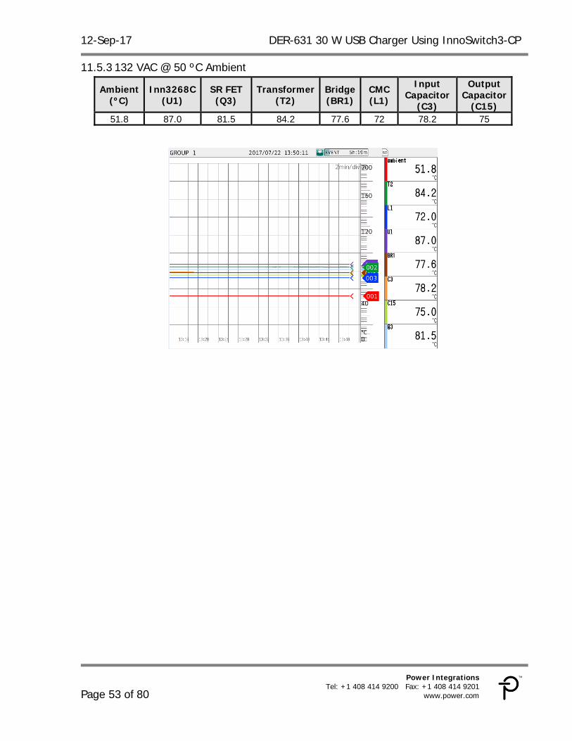
Open Case at 9.2 V / 3.3 A (50 ºC) ............................................................. 51 11.5 100 VAC @ 50 ºC Ambient ................................................................... 51 11.5.1 115VAC @ 50 ºC Ambient .................................................................... 52 11.5.2 132 VAC @ 50 ºC Ambient ................................................................... 53 11.5.3
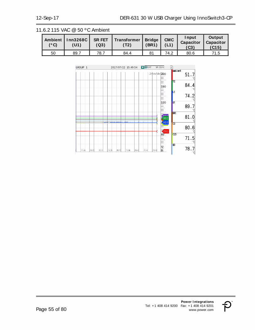
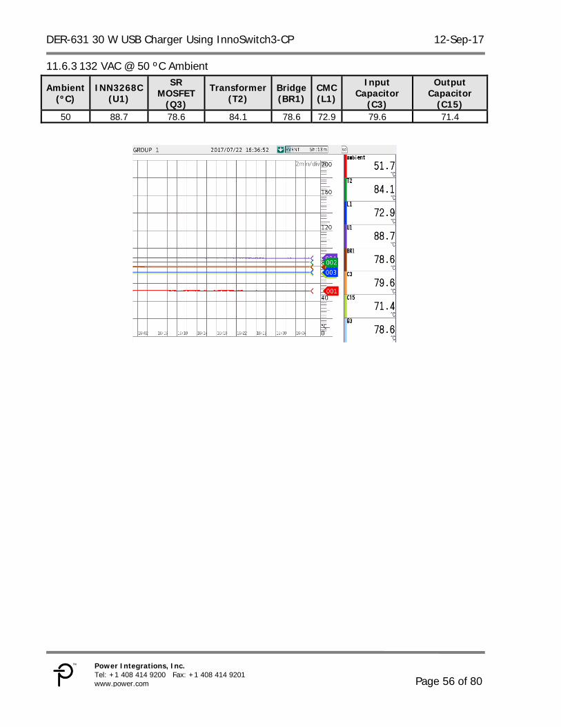
Open Case at 15.3 V / 2 A (50°C) ................................................................ 54 11.6 100 VAC @ 50 ºC Ambient ................................................................... 54 11.6.1 115 VAC @ 50 ºC Ambient ................................................................... 55 11.6.2 132 VAC @ 50 ºC Ambient ................................................................... 56 11.6.3
Waveforms ................................................................................................... 57 12 Load Transient Response (PCB End) ............................................................ 57 12.1
5.1 V Output ....................................................................................... 57 12.1.1 9.2 V Output ....................................................................................... 57 12.1.2 15.3 V Output ..................................................................................... 58 12.1.3
Switching Waveforms ................................................................................. 59 12.2 Drain Voltage and Current (Normal Operation) ...................................... 59 12.2.1 Drain Voltage and Current (Start-up) .................................................... 61 12.2.2 SR MOSFET Voltage ............................................................................ 63 12.2.3 Output Voltage and Current Start-up (End of 100 mΩ Cable) .................. 65 12.2.4
Output Ripple Measurements ...................................................................... 67 12.3 Ripple Measurement Technique ............................................................ 67 12.3.1
Conducted EMI ............................................................................................. 70 13 Test Set-up ............................................................................................... 70 13.1
Equipment and Load Used ................................................................... 70 13.1.1 EMI Test Result ......................................................................................... 71 13.2
Floating Output ................................................................................... 71 13.2.1 Artificial Hand ..................................................................................... 74 13.2.2
DER-631 30 W USB Charger Using InnoSwitch3-CP 12-Sep-17
Page 4 of 80
Power Integrations, Inc. Tel: +1 408 414 9200 Fax: +1 408 414 9201 www.power.com
Line Surge .................................................................................................... 77 14 ESD Test ...................................................................................................... 78 15 Revision History ............................................................................................ 79 16
Important Note: Although this board is designed to satisfy safety isolation requirements, the engineering prototype has not been agency approved. Therefore, all testing should be performed using an isolation transformer to provide the AC input to the prototype board.

12-Sep-17 DER-631 30 W USB Charger Using InnoSwitch3-CP
Page 5 of 80
Power Integrations Tel: +1 408 414 9200 Fax: +1 408 414 9201
www.power.com
Introduction 1This engineering report describes an output power supply intended for USB wall outlet charger. The 30 W output (selectable 5.1 V / 6 A or 9.2 V / 3.3 A or 15.3 V / 2 A) rail is designed for a high power USB charging with Type-A or Type-C ports. The output utilizes INN3268C from the InnoSwitch3-CP family of ICs. This design shows high power density and efficiency that is possible due to the high level of integration of the InnoSwitch3-CP controller providing exceptional performance. DER-631 is a low-line input flyback converter design. The key design goals were high power density, high efficiency, low no load consumption, and best in class thermal performance. This is intended for wall outlet USB chargers. This document contains the power supply specification, schematic diagram, bill of materials, printed circuit layout, and performance data.
Figure 1 – Populated Circuit Board, Top View.
Figure 2 – Populated Circuit Board, Bottom View.

DER-631 30 W USB Charger Using InnoSwitch3-CP 12-Sep-17
Page 6 of 80
Power Integrations, Inc. Tel: +1 408 414 9200 Fax: +1 408 414 9201 www.power.com
Power Supply Specification 2The table below represents the minimum acceptable performance of the design. Actual performance is listed in the results section.
Description Symbol Min Typ Max Units Comment Input
Voltage VIN 100 115 132 VAC 2 Wire – no P.E.
Frequency fLINE 47 60 63 Hz
No-load Input Power (115 VAC) 30 mW Measured at 115 VAC.
5 V Output
Output Voltage VOUT 5.1 V 3%
Output Ripple Voltage VRIPPLE 150 mV At End of Cable. Cable Needs a Resistance of 100 mΩ.
Output Current IOUT 6 6.3 A 20 MHz Bandwidth.
9 V Output
Output Voltage VOUT 9.2 V 5%
Output Ripple Voltage VRIPPLE 150 mV At End of Cable. Cable Needs a Resistance of 100 mΩ.
Output Current IOUT 3.3 A 20 MHz Bandwidth.
15 V Output
Output Voltage VOUT 15.3 V 5%
Output Ripple Voltage VRIPPLE 150 mV At End of Cable. Cable Needs a Resistance of 100 mΩ.
Output Current IOUT 2 A 20 MHz Bandwidth.
Continuous Output Power POUT 30 W
Conducted EMI Meets CISPR22B / EN55022B
Safety Designed to meet IEC60950 / UL1950 Class II
Ambient Temperature TAMB 0 50 oC Free Convection, Sea Level.
12-Sep-17 DER-631 30 W USB Charger Using InnoSwitch3-CP
Page 7 of 80
Power Integrations Tel: +1 408 414 9200 Fax: +1 408 414 9201
www.power.com
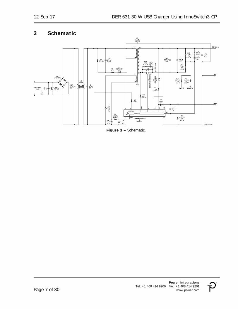
Schematic 3
Figure 3 – Schematic.
DER-631 30 W USB Charger Using InnoSwitch3-CP 12-Sep-17
Page 8 of 80
Power Integrations, Inc. Tel: +1 408 414 9200 Fax: +1 408 414 9201 www.power.com
Circuit Description 4The InnoSwitch3-CP IC combines primary, secondary and feedback circuits in a single surface mounted off-line flyback switcher IC. The IC incorporates the primary MOSFET, the primary-side controller, the secondary-side controller for synchronous rectification and the FluxlinkTM technology that eliminates the need for an optocoupler needed on a secondary sensed feedback system.
Input Circuit Description 4.1Fuse F1 isolates the circuit and provides protection from component failure, and the capacitor C1 provides attenuation for EMI. Common mode inductor L1 and capacitors C3 and C17 form a –filter that provides filtering for both common mode and differential mode noise. Bridge rectifiers BR1 rectifies the AC line voltage and provides a full wave rectified DC across the input capacitors C3 and C17.
Primary Circuit 4.2One end of the transformer T2 primary is connected to the rectified DC bus; the other is connected to the drain terminal of the MOSFET inside the INN3268C (U1). A low cost RCD clamp formed by diode D1, resistors R5 and R21, and capacitor C18 limits the peak Drain voltage of U1 at the instant turn-off of the MOSFET. The clamp helps dissipate the energy stored in the leakage reactance of transformer T2. The IC is kick-started by an internal high-voltage current source that charges the BPP pin capacitor C5 when AC is first applied. During normal operation the primary-side block is powered from an auxiliary winding on the transformer. The output of this is configured as a flyback winding which is rectified and filtered using diode D2 and capacitor C6. Resistor R8 limits the current being supplied to the BPP pin of the InnoSwitch3-CP (U1). An R-C network can be placed across D2 to offer damping of the high frequency ringing, which can reduce radiated EMI. The primary-side controller has a current limit threshold ramp that is inversely proportional to time from the end of the last primary switching cycle. The nature of this characteristic introduces a primary current limit that reduces as the switching frequency reduces. It is similar to the state machine of ON/OFF control but the reduction is now linear in nature rather than the discrete jumps in current limit that the ON/OFF state machine introduces. This produces a primary MOSFET switching pulse train that looks similar to a traditional PWM waveform under steady state conditions with consistent time and peak current between cycles rather than the ON/OFF cycle skipping. This algorithm enables the most efficient use of the primary switch with the benefit that this algorithm responds to digital feedback information where the start of the next switching cycle is immediate when a feedback switching cycle request is received.
12-Sep-17 DER-631 30 W USB Charger Using InnoSwitch3-CP
Page 9 of 80
Power Integrations Tel: +1 408 414 9200 Fax: +1 408 414 9201
www.power.com
Resistor R19 provides line voltage sensing and supplies a current to the V pin of U1, which is proportional to the DC voltage across capacitor C3. At approximately 55 V DC, the current through this resistor exceeds the line undervoltage threshold, which results in enabling of U1. At approximately 250 V DC, the current through this resistor exceeds the line overvoltage threshold, which results in disabling of U1.
Secondary Circuit 4.3The secondary-side of the INN3268C IC provides output voltage, output current sensing and drive a MOSFET providing synchronous rectification. The secondary of the transformer is rectified by MOSFET Q3 and filtered by capacitors C14 and C15. High frequency ringing during switching transients that would otherwise create radiated EMI is reduced via RC snubber, R13 and C8. The gate of Q3 is turned on by the secondary-side controller inside IC U1, based on the winding voltage sensed via resistor R10 and fed into the FWD pin of the IC. In continuous conduction mode operation, the power MOSFET is turned off just prior to the secondary-side controller commanding a new switching cycle from the primary. In discontinuous mode the MOSFET is turned off when the voltage drop across the MOSFET falls below ground. Secondary-side control of the primary-side MOSFET ensures that it is never on at the same time with the synchronous rectification MOSFET on time. The MOSFET drive signal is the output on the SR pin. The secondary side of the IC is self-powered from either the secondary winding forward voltage or the output voltage. The output voltage powers the device then fed into VO pin and charges the decoupling capacitor C9 via an internal regulator. During CC operation, when the output voltage falls, the device will power itself from the secondary winding directly. During the on-time of the primary-side power MOSFET, the forward voltage that appears across the secondary winding is used to charge the decoupling capacitor C9 via resistor R10 and an internal regulator. This allows output current regulation to be maintained down to ~3.0 V. Below this level the unit enters auto-restart until the output load is reduced. Output current is sensed by monitoring the voltage drop across resistors R16 between the IS and GND pins with a threshold of approximately 30 mV to reduce losses. Once the internal current sense threshold is exceeded the device adjusts the number of switch pulses to maintain a fixed output current. If no fixed current requirement, the IS and GND pins can be shorted. Below the CC threshold, the device operates in constant voltage mode. Output voltage is regulated so as to achieve an internal reference voltage of 1.265 V on the FB pin. Capacitor C12 form a phase-lead network that ensures stable operation and minimizes

DER-631 30 W USB Charger Using InnoSwitch3-CP 12-Sep-17
Page 10 of 80
Power Integrations, Inc. Tel: +1 408 414 9200 Fax: +1 408 414 9201 www.power.com
output voltage overshoot and undershoot during transient load conditions. Capacitor C11 provides noise filtering of the signal at the FB pin. Resistors R14 and R15 form the feedback divider network to sense the output voltage. To change the output to 9 V, resistor R22 is added in parallel to the bottom resistor R15. And to change the output to 15 V, resistor R23 is added in parallel to the bottom resistor R15.To vary the output voltage using a USB PD interface, the ports must be connected to the terminals 9V_FB and GND to make it a 9 V output and to the terminals 15V_FB and GND to make it a 15 V output. VR1 protects the power supply from output overvoltage. If the output voltage exceeds VR1 + BPS voltage, current will flow through the BPS pin that will result to auto-restart. A 15 V Zener regulator was used to not exceed the voltage rating of the output capacitors. In order to improve conversion efficiency and reduce switching losses, InnoSwitch3-CP introduces a secondary-based QR functionality. The secondary controller has a means to allow switching when the voltage across the primary switch is near its minimum voltage when the converter operates in critical (CRM) or discontinuous conduction mode (DCM). Rather than detecting the magnetizing ring valley on the primary-side, the peak voltage of the FW pin voltage as it rises above the output voltage level is used to gate secondary request to initiate the switch “on” cycle in the primary controller.
Design Key Points 4.4The design targets greater than 90% average efficiency for the 3 outputs. Efficiency was optimized with transformer design, chosen active devices and bias voltages. For the transformer design, it is best to keep the reflected voltage (VOR) low to decrease the RMS current on the secondary side. Lower VOR also means lower drain to source voltage on the primary side MOSFET that can reduce switching loss. In this design, the VOR was set to 50 V for the 5 V output. This will make the operation of the 5 V output in continuous mode (CCM), but this will ensure the 9 V and 15 V output operations in discontinuous mode (DCM) with valley switching. InnoSwitch3-CP switches up to the 4th valley to achieve better efficiency. Always note that further lowering the VOR can lead to a very large leading edge spike on the primary current because of deep CCM operation. This can trigger the SOA peak limit protection that will result to auto-restart. Aside from the VOR consideration it is also important to lower the leakage inductance of the transformer. The energy being stored in the leakage inductance which is dissipated on the clamping circuit contributes to lower efficiency. Reducing the leakage is an utmost important in this design, to significantly increase the efficiency. A sandwich winding was used to lower the leakage inductance to a value less than 5 H (< 2% of magnetizing inductance). Detailed transformer construction is described on section 7 of this report.
12-Sep-17 DER-631 30 W USB Charger Using InnoSwitch3-CP
Page 11 of 80
Power Integrations Tel: +1 408 414 9200 Fax: +1 408 414 9201
www.power.com
For higher efficiency, it is also necessary to choose the active devices that offer lower conduction losses. For the InnoSwitch3-CP family, INN3268C offers the lowest RDS(On). For the secondary rectifier (SR), a MOSFET was chosen instead of a Schottky diode. A MOSFET of 2.8 mΩ RDS(ON) was used in the design. An added Schottky diode in parallel with the SR MOSFET gives a slight improvement on the efficiency. This diode conducts instead of the MOSFET body diode during the start of secondary MOSFET ON and before the secondary current reaches zero or secondary MOSFET OFF. These delays on transition are needed to avoid cross-conduction with the primary MOSFET. The sweet spot (efficiency and small form factor consideration) for switching frequency operation is at the range from 70 kHz to 80 kHz. An EQ20 transformer with AE of 60 mm2
is enough without saturating the core. The design chooses the minimum number of secondary turns at 390 mT flux density. Auxiliary bias voltage was chosen at range from 8 V to 10 V at no-load condition. This helps improves no load consumption as well as light load efficiency.

DER-631 30 W USB Charger Using InnoSwitch3-CP 12-Sep-17
Page 12 of 80
Power Integrations, Inc. Tel: +1 408 414 9200 Fax: +1 408 414 9201 www.power.com
PCB Layout 5
Figure 4 – Top Side.
Figure 5 – Bottom Side.

12-Sep-17 DER-631 30 W USB Charger Using InnoSwitch3-CP
Page 13 of 80
Power Integrations Tel: +1 408 414 9200 Fax: +1 408 414 9201
www.power.com
Bill of Materials 6
Item Qty Ref Des Description Mfg Part Number Mfg
1 1 BR1 RECT BRIDGE, GP, 600V, 2A, Z4-D Z4GP206L-HF Comchip 2 1 C1 47 nF, 310 VAC, Polyester Film, X2 BFC233920473 Vishay 3 2 C3 C17 27 F, 200 V, Electrolytic, (10 x 16), EKXJ201ELL270MJ16S Nippon Chemi-Con 4 1 C5 0.47 F, 10%, 16V, X7R, 0603 GRM188R71C474KA88D Murata 5 1 C6 22 F, 35 V, Ceramic, X5R, 1206 C3216X5R1V226M160AC TDK 6 1 C7 2.2 nF, Ceramic, Y1 CD90ZU2GA222MYNKA TDK 7 1 C8 470 pF, 200 V, Ceramic, X7R, 0603 06032C471KAT2A AVX 8 1 C9 2.2 F, 10 V, Ceramic, X7R, 0603 GRM188R71A225KE15D Murata 9 1 C11 330 pF 50 V, Ceramic, X7R, 0603 CC0603KRX7R9BB331 Yageo 10 1 C12 4.7 nF 50 V, Ceramic, X7R, 0603 GRM188R71H472KA01D Murata 11 1 C13 1 F 35 V, Ceramic, X7R, 0603 C1608X7R1V105M TDK
12 2 C14 C15 560 F, 25 V,±20%, Al Organic Polymer, A750MS567M1EAAE015 Kemet
13 1 C18 470 pF, ±10%, 500 V, X7R, Ceramic Capacitor, CC1206KKX7RBBB471 Yageo 14 1 D1 600 V, 1 A, Rectifier, Glass Passivated, POWERDI123 DFLR1600-7 Diodes, Inc. 15 1 D2 250 V, 0.2 A, Fast Switching, 50 ns, SOD-323 BAV21WS-7-F Diode, Inc. 16 1 D4 100 V, 2 A, Schottky, SMA STPS2H100AY ST Micro 17 1 F1 1 A, 250 V, Slow, Long Time Lag, RST 1 RST 1 Belfuse 18 1 L1 10 mH, 0.7 A, Common Mode Choke 744821110 Wurth 19 1 Q3 MOSFET, N-CH, 60 V, 100 A , SMD, PG-TDSON-8 BSC028N06LS3GATMA1 Infineon 20 1 R5 RES, 51 , 5%, 1/4 W, Thick Film, 1206 ERJ-8GEYJ510V Panasonic 21 1 R8 RES, 10 k, 5%, 1/10 W, Thick Film, 0603 ERJ-3GEYJ103V Panasonic 22 1 R10 RES, 47 , 5%, 1/10 W, Thick Film, 0603 ERJ-3GEYJ470V Panasonic 23 1 R13 RES, 4.7 , 5%, 1/10 W, Thick Film, 0603 ERJ-3GEYJ4R7V Panasonic 24 1 R14 RES, 100 k, 1%, 1/16 W, Thick Film, 0603 ERJ-3EKF1003V Panasonic 25 1 R15 RES, SMD, 33 k, 1%, 1/10 W, ±100ppm/°C, 0603 RC0603FR-0733KL Yageo 26 1 R16 RES, 0.005 , 0.5 W, 1%, 0805 PMR10EZPFU5L00 Rohm 27 1 R19 RES, 2.2 M, 5%, 1/4 W, Thick Film, 1206 ERJ-8GEYJ225V Panasonic 28 1 R21 RES, 200 k, 5%, 1/4 W, Thick Film, 1206 ERJ-8GEYJ204V Panasonic 29 1 R22 RES, 32.4 k, 1%, 1/16 W, Thick Film, 0603 ERJ-3EKF3242V Panasonic 30 1 R23 RES, 12.4 k, 1%, 1/16 W, Thick Film, 0603 ERJ-3EKF1242V Panasonic 31 1 R24 RES, 0 , 5%, 1/10 W, Thick Film, 0603 ERJ-3GEY0R00V Panasonic 32 1 R25 RES, 1 k, 5%, 1/10 W, Thick Film, 0603 ERJ-3GEYJ102V Panasonic 33 1 RV1 275 VAC, 23 J, 7 mm, RADIAL V275LA4P Littlefuse 34 1 T2 Bobbin, EQ20, 10 pins, 5pri, 5sec P-2042 Pinshine 35 1 U1 InnoSwitch3-CP, InSOP24 INN3268C-H202 Power Integrations 36 1 VR1 15 V, 5%, 500 mW, SOD-123 MMSZ5245B-E3-08 Vishay
DER-631 30 W USB Charger Using InnoSwitch3-CP 12-Sep-17
Page 14 of 80
Power Integrations, Inc. Tel: +1 408 414 9200 Fax: +1 408 414 9201 www.power.com
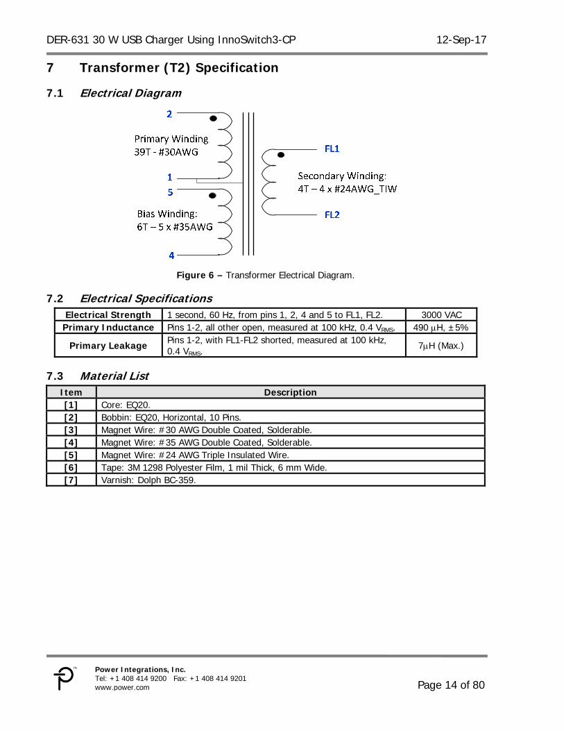
Transformer (T2) Specification 7
Electrical Diagram 7.1
Figure 6 – Transformer Electrical Diagram.
Electrical Specifications 7.2Electrical Strength 1 second, 60 Hz, from pins 1, 2, 4 and 5 to FL1, FL2. 3000 VAC
Primary Inductance Pins 1-2, all other open, measured at 100 kHz, 0.4 VRMS. 490 H, ±5%
Primary Leakage Pins 1-2, with FL1-FL2 shorted, measured at 100 kHz, 0.4 VRMS.
7H (Max.)
Material List 7.3Item Description [1] Core: EQ20. [2] Bobbin: EQ20, Horizontal, 10 Pins. [3] Magnet Wire: #30 AWG Double Coated, Solderable. [4] Magnet Wire: #35 AWG Double Coated, Solderable. [5] Magnet Wire: #24 AWG Triple Insulated Wire. [6] Tape: 3M 1298 Polyester Film, 1 mil Thick, 6 mm Wide. [7] Varnish: Dolph BC-359.

12-Sep-17 DER-631 30 W USB Charger Using InnoSwitch3-CP
Page 15 of 80
Power Integrations Tel: +1 408 414 9200 Fax: +1 408 414 9201
www.power.com
Transformer Build Diagram 7.4
Figure 7 – Transformer Build Diagram.
Transformer Construction 7.5Winding
preparation Place the bobbin Item [2] on the mandrel with the pin side is on the left side. Winding direction is clockwise direction.
WD1 1st Primary
Start at pin 2, wind 20 turns of wire Item [3] in 1 layer. At the last turn, bring wire back to the left side.
Insulation Place 1 layer of tape Item [6] for insulation.
WD2 Bias/Shield
Start at pin 5, wind 6 (5-filars) turns of wire Item [4] in 1 layer. At the last turn, bring bifilar wire back to the left finish at pin 4. Cut the remaining trifilar wire then no connect.
Insulation Place 1 layer of tape Item [6] for insulation. WD3
Secondary Start at FL1 from the left side of the bobbin, wind 4 bifilar turns of wire Item [5] in 1 layer. At the last turn, finish winding at FL2.
Insulation Place 1 layer of tape Item [6] for insulation. WD4
2nd Primary Continue primary winding of 19 turns from left to right. At the last turn finish at pin 1.
Insulation Place 1 layer of tape Item [6] for insulation. WD5
2nd Primary Start at FL1 from the left side of the bobbin, wind 4 bifilar turns of wire Item [5] in 1 layer. At the last turn, finish winding at FL2.
Insulation Place 3 layers of tape Item [6] for insulation and secure the windings.
Core shield Gap core halves to get 490 H inductance. Secure core and wind bifilar tin wire around the core. Terminate the wire at pin 1.
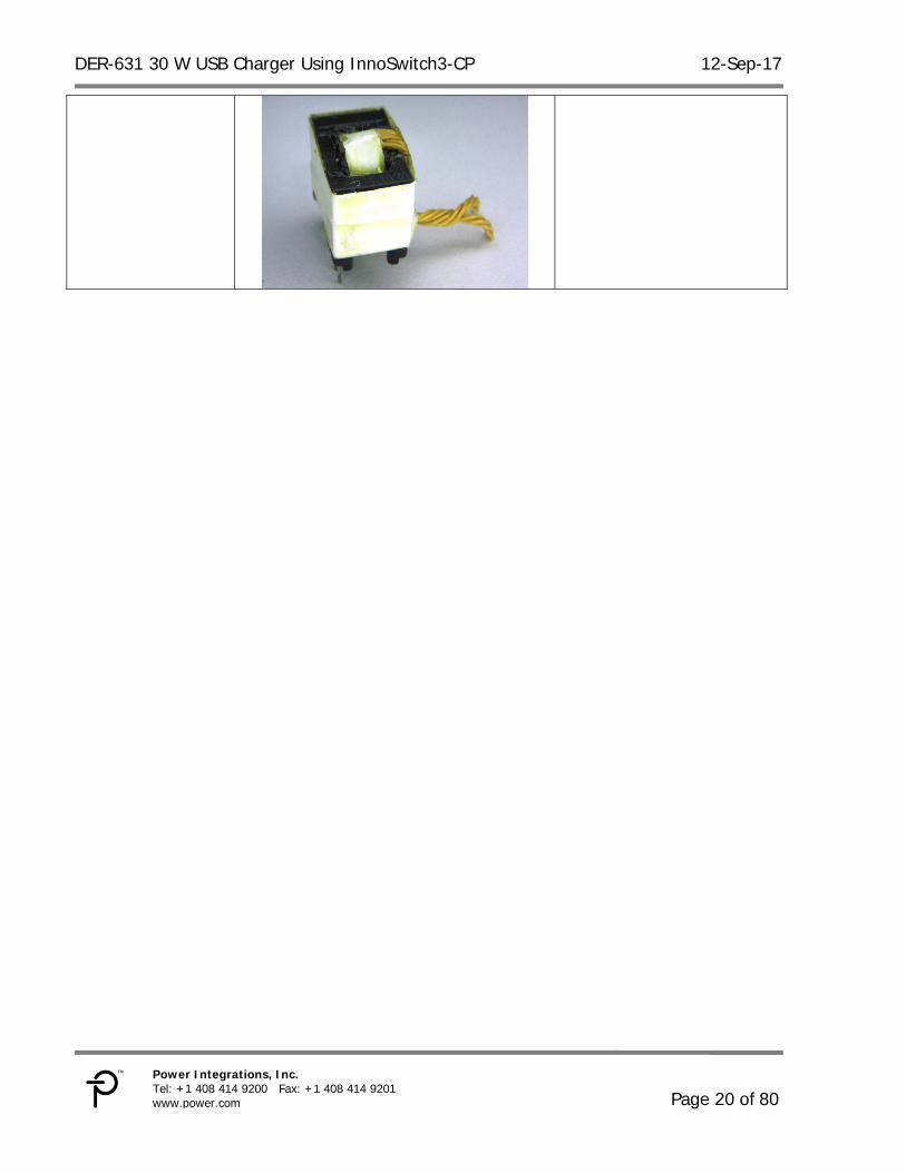
Finish Assembly Cover core with 2 layers of tape. Varnish Item [7].
DER-631 30 W USB Charger Using InnoSwitch3-CP 12-Sep-17
Page 16 of 80
Power Integrations, Inc. Tel: +1 408 414 9200 Fax: +1 408 414 9201 www.power.com
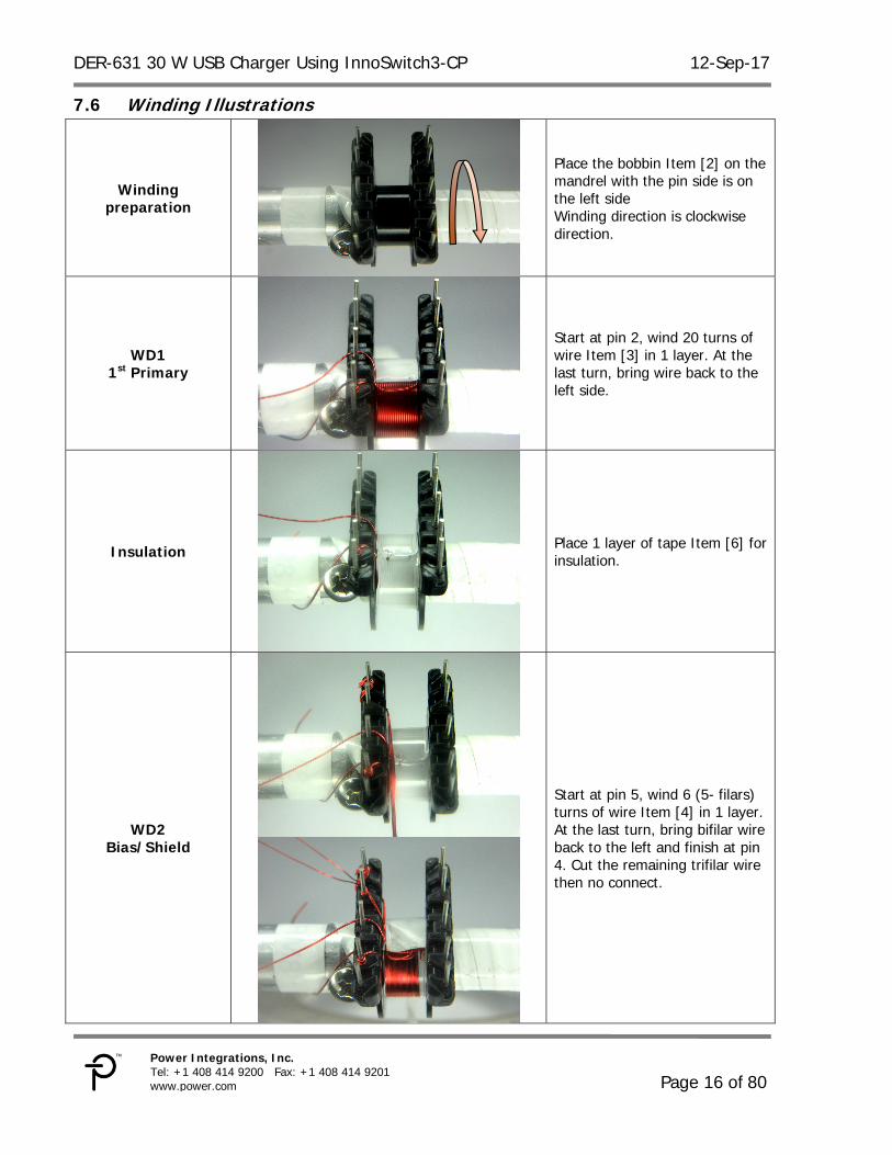
Winding Illustrations 7.6
Winding preparation
Place the bobbin Item [2] on the mandrel with the pin side is on the left side Winding direction is clockwise direction.
WD1 1st Primary
Start at pin 2, wind 20 turns of wire Item [3] in 1 layer. At the last turn, bring wire back to the left side.
Insulation
Place 1 layer of tape Item [6] for insulation.
WD2 Bias/Shield
Start at pin 5, wind 6 (5- filars) turns of wire Item [4] in 1 layer. At the last turn, bring bifilar wire back to the left and finish at pin 4. Cut the remaining trifilar wire then no connect.
12-Sep-17 DER-631 30 W USB Charger Using InnoSwitch3-CP
Page 17 of 80
Power Integrations Tel: +1 408 414 9200 Fax: +1 408 414 9201
www.power.com
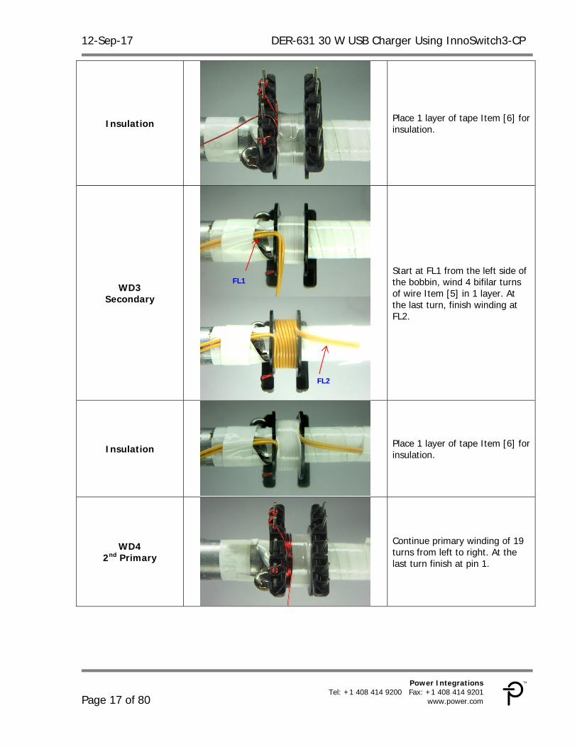
Insulation
Place 1 layer of tape Item [6] for insulation.
WD3 Secondary
Start at FL1 from the left side of the bobbin, wind 4 bifilar turns of wire Item [5] in 1 layer. At the last turn, finish winding at FL2.
Insulation
Place 1 layer of tape Item [6] for insulation.
WD4 2nd Primary
Continue primary winding of 19 turns from left to right. At the last turn finish at pin 1.
FL1
FL2

DER-631 30 W USB Charger Using InnoSwitch3-CP 12-Sep-17
Page 18 of 80
Power Integrations, Inc. Tel: +1 408 414 9200 Fax: +1 408 414 9201 www.power.com
Insulation
Place 1 layer of tape Item [6] for insulation.
WD5 Secondary
Start at FL1 from the left side of the bobbin, wind 4 bifilar turns of wire Item [5] in 1 layer. At the last turn, finish winding at FL2.
Insulation
Place 3 layers of tape Item [6] for insulation and bring FL1 to right side then secure the windings.
FL1
FL2
12-Sep-17 DER-631 30 W USB Charger Using InnoSwitch3-CP
Page 19 of 80
Power Integrations Tel: +1 408 414 9200 Fax: +1 408 414 9201
www.power.com
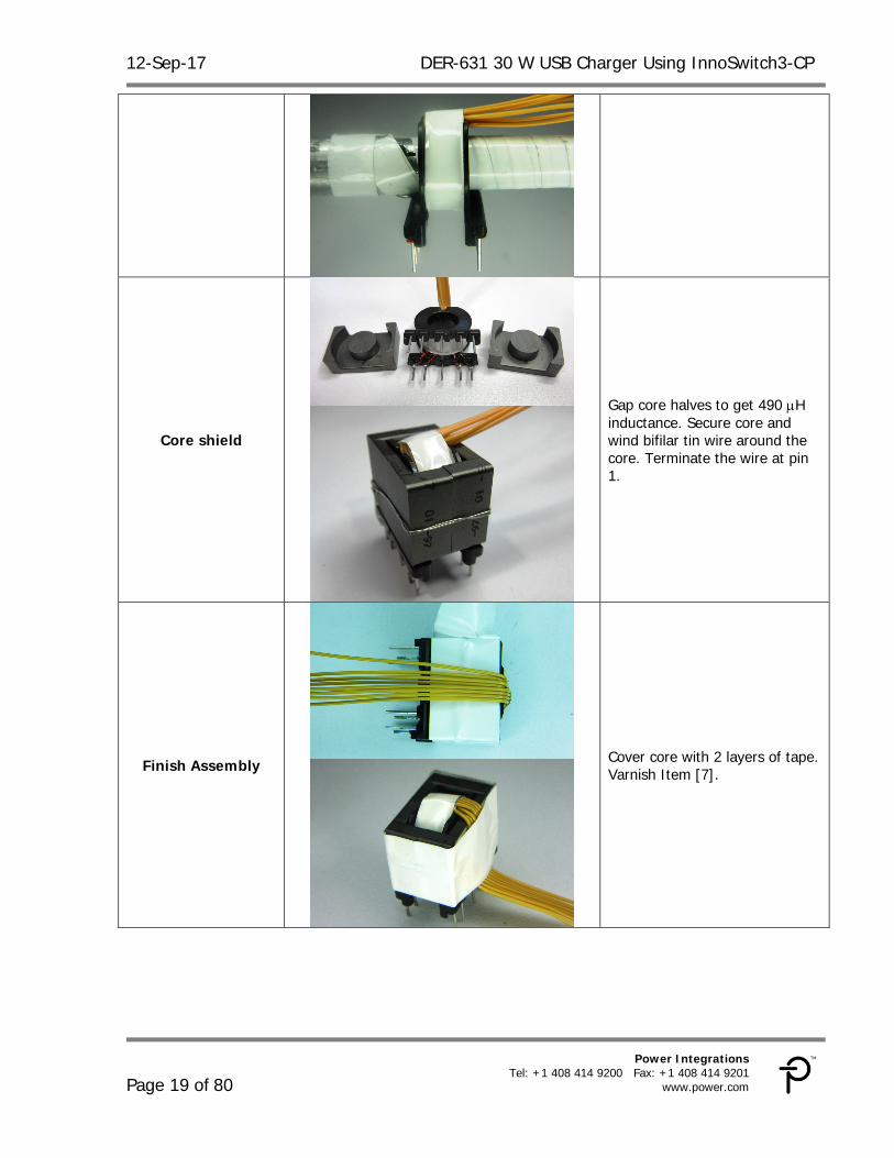
Core shield
Gap core halves to get 490 H inductance. Secure core and wind bifilar tin wire around the core. Terminate the wire at pin 1.
Finish Assembly
Cover core with 2 layers of tape. Varnish Item [7].
DER-631 30 W USB Charger Using InnoSwitch3-CP 12-Sep-17
Page 20 of 80
Power Integrations, Inc. Tel: +1 408 414 9200 Fax: +1 408 414 9201 www.power.com
12-Sep-17 DER-631 30 W USB Charger Using InnoSwitch3-CP
Page 21 of 80
Power Integrations Tel: +1 408 414 9200 Fax: +1 408 414 9201
www.power.com
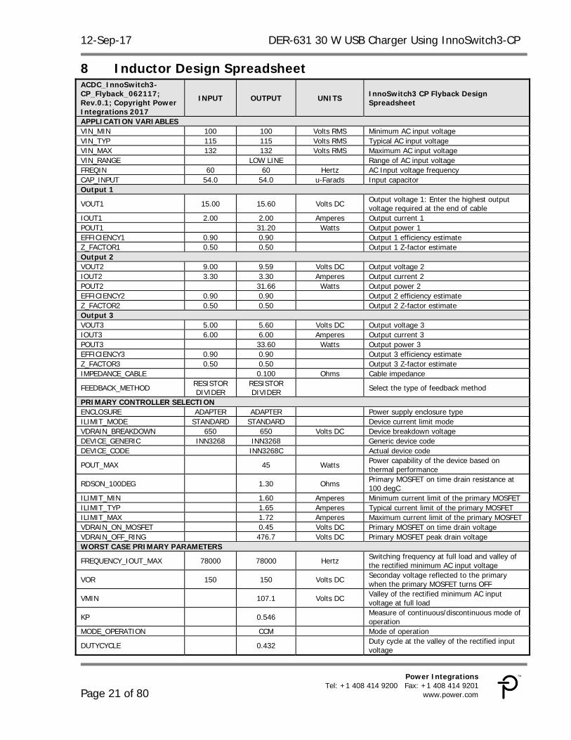
Inductor Design Spreadsheet 8ACDC_InnoSwitch3-CP_Flyback_062117; Rev.0.1; Copyright Power Integrations 2017
INPUT OUTPUT UNITS InnoSwitch3 CP Flyback Design Spreadsheet
APPLICATION VARIABLES VIN_MIN 100 100 Volts RMS Minimum AC input voltage VIN_TYP 115 115 Volts RMS Typical AC input voltage VIN_MAX 132 132 Volts RMS Maximum AC input voltage VIN_RANGE LOW LINE Range of AC input voltage FREQIN 60 60 Hertz AC Input voltage frequency CAP_INPUT 54.0 54.0 u-Farads Input capacitor Output 1
VOUT1 15.00 15.60 Volts DC Output voltage 1: Enter the highest output voltage required at the end of cable
IOUT1 2.00 2.00 Amperes Output current 1 POUT1 31.20 Watts Output power 1 EFFICIENCY1 0.90 0.90 Output 1 efficiency estimate Z_FACTOR1 0.50 0.50 Output 1 Z-factor estimate Output 2 VOUT2 9.00 9.59 Volts DC Output voltage 2 IOUT2 3.30 3.30 Amperes Output current 2 POUT2 31.66 Watts Output power 2 EFFICIENCY2 0.90 0.90 Output 2 efficiency estimate Z_FACTOR2 0.50 0.50 Output 2 Z-factor estimate Output 3 VOUT3 5.00 5.60 Volts DC Output voltage 3 IOUT3 6.00 6.00 Amperes Output current 3 POUT3 33.60 Watts Output power 3 EFFICIENCY3 0.90 0.90 Output 3 efficiency estimate Z_FACTOR3 0.50 0.50 Output 3 Z-factor estimate IMPEDANCE_CABLE 0.100 Ohms Cable impedance
FEEDBACK_METHOD RESISTOR DIVIDER
RESISTOR DIVIDER Select the type of feedback method
PRIMARY CONTROLLER SELECTION ENCLOSURE ADAPTER ADAPTER Power supply enclosure type ILIMIT_MODE STANDARD STANDARD Device current limit mode VDRAIN_BREAKDOWN 650 650 Volts DC Device breakdown voltage DEVICE_GENERIC INN3268 INN3268 Generic device code DEVICE_CODE INN3268C Actual device code
POUT_MAX 45 Watts Power capability of the device based on thermal performance
RDSON_100DEG 1.30 Ohms Primary MOSFET on time drain resistance at 100 degC
ILIMIT_MIN 1.60 Amperes Minimum current limit of the primary MOSFET ILIMIT_TYP 1.65 Amperes Typical current limit of the primary MOSFET ILIMIT_MAX 1.72 Amperes Maximum current limit of the primary MOSFET VDRAIN_ON_MOSFET 0.45 Volts DC Primary MOSFET on time drain voltage VDRAIN_OFF_RING 476.7 Volts DC Primary MOSFET peak drain voltage WORST CASE PRIMARY PARAMETERS
FREQUENCY_IOUT_MAX 78000 78000 Hertz Switching frequency at full load and valley of the rectified minimum AC input voltage
VOR 150 150 Volts DC Seconday voltage reflected to the primary when the primary MOSFET turns OFF
VMIN 107.1 Volts DC Valley of the rectified minimum AC input voltage at full load
KP 0.546 Measure of continuous/discontinuous mode of operation
MODE_OPERATION CCM Mode of operation
DUTYCYCLE 0.432 Duty cycle at the valley of the rectified input voltage
DER-631 30 W USB Charger Using InnoSwitch3-CP 12-Sep-17
Page 22 of 80
Power Integrations, Inc. Tel: +1 408 414 9200 Fax: +1 408 414 9201 www.power.com
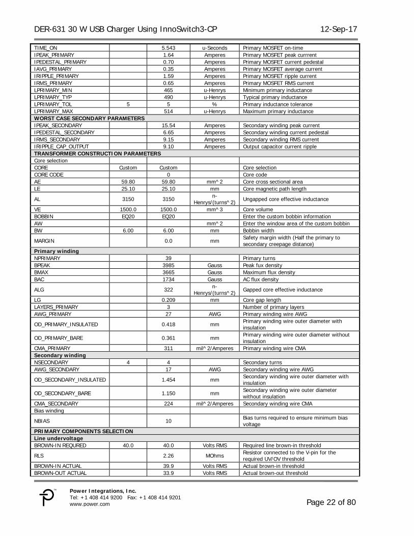
TIME_ON 5.543 u-Seconds Primary MOSFET on-time IPEAK_PRIMARY 1.64 Amperes Primary MOSFET peak currrent IPEDESTAL_PRIMARY 0.70 Amperes Primary MOSFET current pedestal IAVG_PRIMARY 0.35 Amperes Primary MOSFET average current IRIPPLE_PRIMARY 1.59 Amperes Primary MOSFET ripple current IRMS_PRIMARY 0.65 Amperes Primary MOSFET RMS current LPRIMARY_MIN 465 u-Henrys Minimum primary inductance LPRIMARY_TYP 490 u-Henrys Typical primary inductance LPRIMARY_TOL 5 5 % Primary inductance tolerance LPRIMARY_MAX 514 u-Henrys Maximum primary inductance WORST CASE SECONDARY PARAMETERS IPEAK_SECONDARY 15.54 Amperes Secondary winding peak current IPEDESTAL_SECONDARY 6.65 Amperes Secondary winding current pedestal IRMS_SECONDARY 9.15 Amperes Secondary winding RMS current IRIPPLE_CAP_OUTPUT 9.10 Amperes Output capacitor current ripple TRANSFORMER CONSTRUCTION PARAMETERS Core selection CORE Custom Custom Core selection CORE CODE 0 Core code AE 59.80 59.80 mm^2 Core cross sectional area LE 25.10 25.10 mm Core magnetic path length
AL 3150 3150 n-Henrys/(turns^2) Ungapped core effective inductance
VE 1500.0 1500.0 mm^3 Core volume BOBBIN EQ20 EQ20 Enter the custom bobbin information AW mm^2 Enter the window area of the custom bobbin BW 6.00 6.00 mm Bobbin width
MARGIN 0.0 mm Safety margin width (Half the primary to secondary creepage distance)
Primary winding NPRIMARY 39 Primary turns BPEAK 3985 Gauss Peak fux density BMAX 3665 Gauss Maximum flux density BAC 1734 Gauss AC flux density
ALG 322 n-Henrys/(turns^2) Gapped core effective inductance
LG 0.209 mm Core gap length LAYERS_PRIMARY 3 Number of primary layers AWG_PRIMARY 27 AWG Primary winding wire AWG
OD_PRIMARY_INSULATED 0.418 mm Primary winding wire outer diameter with insulation
OD_PRIMARY_BARE 0.361 mm Primary winding wire outer diameter without insulation
CMA_PRIMARY 311 mil^2/Amperes Primary winding wire CMA Secondary winding NSECONDARY 4 4 Secondary turns AWG_SECONDARY 17 AWG Secondary winding wire AWG
OD_SECONDARY_INSULATED 1.454 mm Secondary winding wire outer diameter with insulation
OD_SECONDARY_BARE 1.150 mm Secondary winding wire outer diameter without insulation
CMA_SECONDARY 224 mil^2/Amperes Secondary winding wire CMA Bias winding
NBIAS 10 Bias turns required to ensure minimum bias voltage
PRIMARY COMPONENTS SELECTION Line undervoltage BROWN-IN REQURED 40.0 40.0 Volts RMS Required line brown-in threshold
RLS 2.26 MOhms Resistor connected to the V-pin for the required UV/OV threshold
BROWN-IN ACTUAL 39.9 Volts RMS Actual brown-in threshold BROWN-OUT ACTUAL 33.9 Volts RMS Actual brown-out threshold
12-Sep-17 DER-631 30 W USB Charger Using InnoSwitch3-CP
Page 23 of 80
Power Integrations Tel: +1 408 414 9200 Fax: +1 408 414 9201
www.power.com
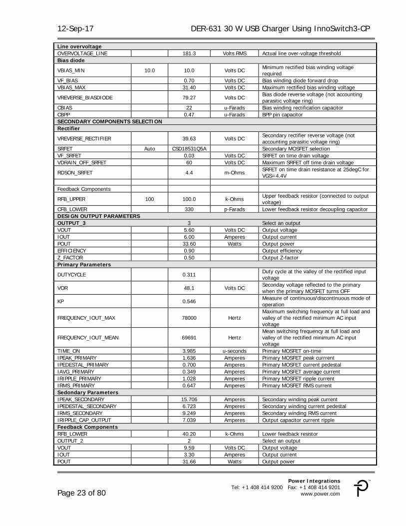
Line overvoltage OVERVOLTAGE_LINE 181.3 Volts RMS Actual line over-voltage threshold Bias diode
VBIAS_MIN 10.0 10.0 Volts DC Minimum rectified bias winding voltage required
VF_BIAS 0.70 Volts DC Bias winding diode forward drop VBIAS_MAX 31.40 Volts DC Maximum rectified bias winding voltage
VREVERSE_BIASDIODE 79.27 Volts DC Bias diode reverse voltage (not accounting parasitic voltage ring)
CBIAS 22 u-Farads Bias winding rectification capacitor CBPP 0.47 u-Farads BPP pin capacitor SECONDARY COMPONENTS SELECTION Rectifier
VREVERSE_RECTIFIER 39.63 Volts DC Secondary rectifier reverse voltage (not accounting parasitic voltage ring)
SRFET Auto CSD18531Q5A Secondary MOSFET selection VF_SRFET 0.03 Volts DC SRFET on time drain voltage VDRAIN_OFF_SRFET 60 Volts DC Maximum SRFET off time drain voltage
RDSON_SRFET 4.4 m-Ohms SRFET on time drain resistance at 25degC for VGS=4.4V
Feedback Components
RFB_UPPER 100 100.0 k-Ohms Upper feedback resistor (connected to output voltage)
CFB_LOWER 330 p-Farads Lower feedback resistor decoupling capacitor DESIGN OUTPUT PARAMETERS OUTPUT_3 3 Select an output VOUT 5.60 Volts DC Output voltage IOUT 6.00 Amperes Output current POUT 33.60 Watts Output power EFFICIENCY 0.90 Output efficiency Z_FACTOR 0.50 Output Z-factor Primary Parameters
DUTYCYCLE 0.311 Duty cycle at the valley of the rectified input voltage
VOR 48.1 Volts DC Seconday voltage reflected to the primary when the primary MOSFET turns OFF
KP 0.546 Measure of continuous/discontinuous mode of operation
FREQUENCY_IOUT_MAX 78000 Hertz Maximum switching frequency at full load and valley of the rectified minimum AC input voltage
FREQUENCY_IOUT_MEAN 69691 Hertz Mean switching frequency at full load and valley of the rectified minimum AC input voltage
TIME_ON 3.985 u-seconds Primary MOSFET on-time IPEAK_PRIMARY 1.636 Amperes Primary MOSFET peak currrent IPEDESTAL_PRIMARY 0.700 Amperes Primary MOSFET current pedestal IAVG_PRIMARY 0.349 Amperes Primary MOSFET average current IRIPPLE_PRIMARY 1.028 Amperes Primary MOSFET ripple current IRMS_PRIMARY 0.647 Amperes Primary MOSFET RMS current Sedondary Parameters IPEAK_SECONDARY 15.706 Amperes Secondary winding peak current IPEDESTAL_SECONDARY 6.723 Amperes Secondary winding current pedestal IRMS_SECONDARY 9.249 Amperes Secondary winding RMS current IRIPPLE_CAP_OUTPUT 7.039 Amperes Output capacitor current ripple Feedback Components RFB_LOWER 40.20 k-Ohms Lower feedback resistor OUTPUT_2 2 Select an output VOUT 9.59 Volts DC Output voltage IOUT 3.30 Amperes Output current POUT 31.66 Watts Output power
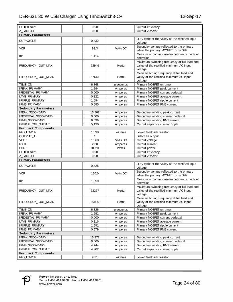
DER-631 30 W USB Charger Using InnoSwitch3-CP 12-Sep-17
Page 24 of 80
Power Integrations, Inc. Tel: +1 408 414 9200 Fax: +1 408 414 9201 www.power.com
EFFICIENCY 0.90 Output efficiency Z_FACTOR 0.50 Output Z-factor Primary Parameters
DUTYCYCLE 0.432 Duty cycle at the valley of the rectified input voltage
VOR 92.3 Volts DC Seconday voltage reflected to the primary when the primary MOSFET turns OFF
KP 1.114 Measure of continuous/discontinuous mode of operation
FREQUENCY_IOUT_MAX 62949 Hertz Maximum switching frequency at full load and valley of the rectified minimum AC input voltage
FREQUENCY_IOUT_MEAN 57613 Hertz Mean switching frequency at full load and valley of the rectified minimum AC input voltage
TIME_ON 6.868 u-seconds Primary MOSFET on-time IPEAK_PRIMARY 1.594 Amperes Primary MOSFET peak currrent IPEDESTAL_PRIMARY 0.000 Amperes Primary MOSFET current pedestal IAVG_PRIMARY 0.322 Amperes Primary MOSFET average current IRIPPLE_PRIMARY 1.594 Amperes Primary MOSFET ripple current IRMS_PRIMARY 0.585 Amperes Primary MOSFET RMS current Sedondary Parameters IPEAK_SECONDARY 15.302 Amperes Secondary winding peak current IPEDESTAL_SECONDARY 0.000 Amperes Secondary winding current pedestal IRMS_SECONDARY 6.099 Amperes Secondary winding RMS current IRIPPLE_CAP_OUTPUT 5.130 Amperes Output capacitor current ripple Feedback Components RFB_LOWER 16.90 k-Ohms Lower feedback resistor OUTPUT_1 1 Select an output VOUT 15.60 Volts DC Output voltage IOUT 2.00 Amperes Output current POUT 31.20 Watts Output power EFFICIENCY 0.90 Output efficiency Z_FACTOR 0.50 Output Z-factor Primary Parameters
DUTYCYCLE 0.425 Duty cycle at the valley of the rectified input voltage
VOR 150.0 Volts DC Seconday voltage reflected to the primary when the primary MOSFET turns OFF
KP 1.859 Measure of continuous/discontinuous mode of operation
FREQUENCY_IOUT_MAX 62257 Hertz Maximum switching frequency at full load and valley of the rectified minimum AC input voltage
FREQUENCY_IOUT_MEAN 56995 Hertz Mean switching frequency at full load and valley of the rectified minimum AC input voltage
TIME_ON 6.826 u-seconds Primary MOSFET on-time IPEAK_PRIMARY 1.591 Amperes Primary MOSFET peak currrent IPEDESTAL_PRIMARY 0.000 Amperes Primary MOSFET current pedestal IAVG_PRIMARY 0.316 Amperes Primary MOSFET average current IRIPPLE_PRIMARY 1.591 Amperes Primary MOSFET ripple current IRMS_PRIMARY 0.579 Amperes Primary MOSFET RMS current Sedondary Parameters IPEAK_SECONDARY 15.272 Amperes Secondary winding peak current IPEDESTAL_SECONDARY 0.000 Amperes Secondary winding current pedestal IRMS_SECONDARY 4.744 Amperes Secondary winding RMS current IRIPPLE_CAP_OUTPUT 4.302 Amperes Output capacitor current ripple Feedback Components RFB_LOWER 9.31 k-Ohms Lower feedback resistor

12-Sep-17 DER-631 30 W USB Charger Using InnoSwitch3-CP
Page 25 of 80
Power Integrations Tel: +1 408 414 9200 Fax: +1 408 414 9201
www.power.com
Performance Data 9
Efficiency 9.1Note: Output voltage measured at PCB end. This considers the 300 mV cable drop compensation.
Efficiency vs. Line 9.1.1
Figure 8 – Efficiency vs. Input Line Voltage.
84
86
88
90
92
94
96
95 100 105 110 115 120 125 130 135
Effi
cien
cy (
%)
Input Voltage (VAC)
5.1 V Output9.2 V Output15.3 V Output

DER-631 30 W USB Charger Using InnoSwitch3-CP 12-Sep-17
Page 26 of 80
Power Integrations, Inc. Tel: +1 408 414 9200 Fax: +1 408 414 9201 www.power.com
Efficiency vs. Load 9.1.2Note: Output voltage measured at PCB end. This considers the 300mV cable drop compensation.
Figure 9 – Efficiency vs. Percent Load.
76
78
80
82
84
86
88
90
92
94
0 10 20 30 40 50 60 70 80 90 100
Effi
cien
cy (
%)
Load (%)
5.1 V Output9.2 V Output15.3 V Output

12-Sep-17 DER-631 30 W USB Charger Using InnoSwitch3-CP
Page 27 of 80
Power Integrations Tel: +1 408 414 9200 Fax: +1 408 414 9201
www.power.com
No-Load Input Power 9.1.3Note: 5 V outputs at no-load.
Figure 10 – No Load Power vs. Input Line Voltage.
0
5
10
15
20
25
30
95 100 105 110 115 120 125 130 135
No-
Load
Pow
er (
mW
)
Input Voltage (VAC)

DER-631 30 W USB Charger Using InnoSwitch3-CP 12-Sep-17
Page 28 of 80
Power Integrations, Inc. Tel: +1 408 414 9200 Fax: +1 408 414 9201 www.power.com
Line and Load Regulation 9.2
5.1 V Line Regulation at 6 A Load 9.2.1Note: Output voltage measured at PCB end. This considers the 300 mV cable drop compensation.
Figure 11 – 5.1 V Output Regulation vs. Input Line Voltage.
-3%
-2%
-1%
0%
1%
2%
3%
5.25
5.30
5.35
5.40
5.45
5.50
5.55
95 100 105 110 115 120 125 130 135
Out
put
Vol
tage
(V
)
Load (%)

12-Sep-17 DER-631 30 W USB Charger Using InnoSwitch3-CP
Page 29 of 80
Power Integrations Tel: +1 408 414 9200 Fax: +1 408 414 9201
www.power.com
9.2 V Line Regulation at 3.3 A Load 9.2.2Note: Output voltage measured at PCB end. This considers the 300 mV cable drop compensation.
Figure 12 – 9.2 V Output Regulation vs. Input Line Voltage
-3%
-2%
-1%
0%
1%
2%
3%
9.2
9.3
9.4
9.5
9.6
9.7
9.8
95 100 105 110 115 120 125 130 135
Out
put
Vol
tage
(V
)
Load (%)
DER-631 30 W USB Charger Using InnoSwitch3-CP 12-Sep-17
Page 30 of 80
Power Integrations, Inc. Tel: +1 408 414 9200 Fax: +1 408 414 9201 www.power.com
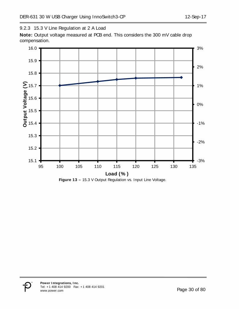
15.3 V Line Regulation at 2 A Load 9.2.3Note: Output voltage measured at PCB end. This considers the 300 mV cable drop compensation.
Figure 13 – 15.3 V Output Regulation vs. Input Line Voltage.
-3%
-2%
-1%
0%
1%
2%
3%
15.1
15.2
15.3
15.4
15.5
15.6
15.7
15.8
15.9
16.0
95 100 105 110 115 120 125 130 135
Out
put
Vol
tage
(V
)
Load (%)

12-Sep-17 DER-631 30 W USB Charger Using InnoSwitch3-CP
Page 31 of 80
Power Integrations Tel: +1 408 414 9200 Fax: +1 408 414 9201
www.power.com
5.1 V Load Regulation 9.2.4Note: Output voltage measured at PCB end. This considers the 300 mV cable drop compensation.
Figure 14 – 5.1 V Output Regulation vs. Percent Load.
5.00
5.05
5.10
5.15
5.20
5.25
5.30
5.35
5.40
5.45
5.50
0 10 20 30 40 50 60 70 80 90 100
Out
put
Vol
tage
(V
)
Load (%)

DER-631 30 W USB Charger Using InnoSwitch3-CP 12-Sep-17
Page 32 of 80
Power Integrations, Inc. Tel: +1 408 414 9200 Fax: +1 408 414 9201 www.power.com
9.2 V Load Regulation 9.2.5Note: Output voltage measured at PCB end. This considers the 300 mV cable drop compensation.
Figure 15 – 9.2 V Output Regulation vs. Percent Load.
9.0
9.1
9.2
9.3
9.4
9.5
0 10 20 30 40 50 60 70 80 90 100
Out
put
Vol
tage
(V
)
Load (%)

12-Sep-17 DER-631 30 W USB Charger Using InnoSwitch3-CP
Page 33 of 80
Power Integrations Tel: +1 408 414 9200 Fax: +1 408 414 9201
www.power.com
15.3 V Load Regulation 9.2.6Note: Output voltage measured at PCB end. This considers the 300 mV cable drop compensation.
Figure 16 – 15.3 V Output Regulation vs. Percent Load.
15.0
15.1
15.2
15.3
15.4
15.5
15.6
15.7
15.8
15.9
16.0
0 10 20 30 40 50 60 70 80 90 100
Out
put
Vol
tage
(V
)
Load (%)
DER-631 30 W USB Charger Using InnoSwitch3-CP 12-Sep-17
Page 34 of 80
Power Integrations, Inc. Tel: +1 408 414 9200 Fax: +1 408 414 9201 www.power.com
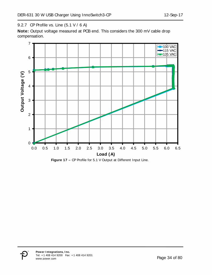
CP Profile vs. Line (5.1 V / 6 A) 9.2.7Note: Output voltage measured at PCB end. This considers the 300 mV cable drop compensation.
Figure 17 – CP Profile for 5.1 V Output at Different Input Line.
0
1
2
3
4
5
6
7
0.0 0.5 1.0 1.5 2.0 2.5 3.0 3.5 4.0 4.5 5.0 5.5 6.0 6.5
Out
put
Vol
tage
(V
)
Load (A)
100 VAC115 VAC135 VAC
12-Sep-17 DER-631 30 W USB Charger Using InnoSwitch3-CP
Page 35 of 80
Power Integrations Tel: +1 408 414 9200 Fax: +1 408 414 9201
www.power.com
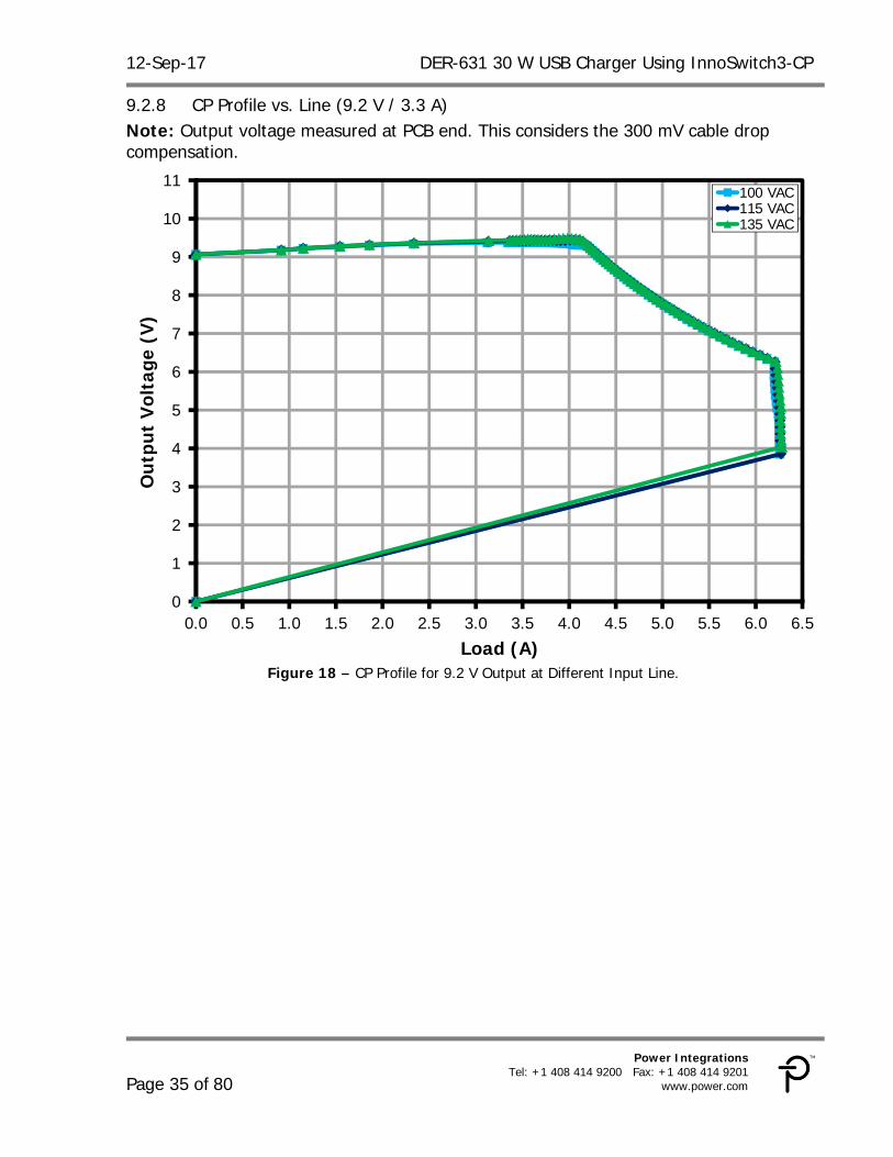
CP Profile vs. Line (9.2 V / 3.3 A) 9.2.8Note: Output voltage measured at PCB end. This considers the 300 mV cable drop compensation.
Figure 18 – CP Profile for 9.2 V Output at Different Input Line.
0
1
2
3
4
5
6
7
8
9
10
11
0.0 0.5 1.0 1.5 2.0 2.5 3.0 3.5 4.0 4.5 5.0 5.5 6.0 6.5
Out
put
Vol
tage
(V
)
Load (A)
100 VAC115 VAC135 VAC
DER-631 30 W USB Charger Using InnoSwitch3-CP 12-Sep-17
Page 36 of 80
Power Integrations, Inc. Tel: +1 408 414 9200 Fax: +1 408 414 9201 www.power.com
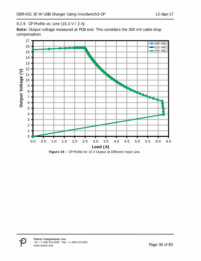
CP Profile vs. Line (15.3 V / 2 A) 9.2.9Note: Output voltage measured at PCB end. This considers the 300 mV cable drop compensation.
Figure 19 – CP Profile for 15 V Output at Different Input Line.
0123456789
1011121314151617
0.0 0.5 1.0 1.5 2.0 2.5 3.0 3.5 4.0 4.5 5.0 5.5 6.0 6.5
Out
put
Vol
tage
(V
)
Load (A)
100 VAC115 VAC135 VAC
12-Sep-17 DER-631 30 W USB Charger Using InnoSwitch3-CP
Page 37 of 80
Power Integrations Tel: +1 408 414 9200 Fax: +1 408 414 9201
www.power.com
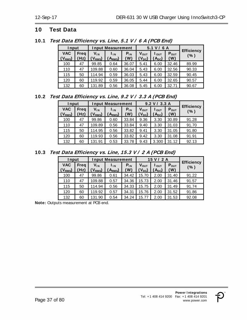
Test Data 10
Test Data Efficiency vs. Line, 5.1 V / 6 A (PCB End) 10.1Input Input Measurement 5.1 V / 6 A
Efficiency (%) VAC
(VRMS) Freq (Hz)
VIN (VRMS)
IIN (ARMS)
PIN (W)
VOUT (VDC)
IOUT (ADC)
POUT (W)
100 47 99.85 0.64 36.07 5.41 6.00 32.46 89.99 110 47 109.88 0.60 36.04 5.43 6.00 32.56 90.33 115 50 114.94 0.59 36.03 5.43 6.00 32.59 90.45 120 60 119.92 0.59 36.05 5.44 6.00 32.65 90.57 132 60 131.89 0.56 36.08 5.45 6.00 32.71 90.67
Test Data Efficiency vs. Line, 9.2 V / 3.3 A (PCB End) 10.2Input Input Measurement 9.2 V / 3.3 A
Efficiency (%) VAC
(VRMS) Freq (Hz)
VIN (VRMS)
IIN (ARMS)
PIN (W)
VOUT (VDC)
IOUT (ADC)
POUT (W)
100 47 99.86 0.60 33.84 9.36 3.30 30.89 91.28 110 47 109.89 0.56 33.84 9.40 3.30 31.03 91.70 115 50 114.95 0.56 33.82 9.41 3.30 31.05 91.80 120 60 119.93 0.56 33.82 9.42 3.30 31.08 91.91 132 60 131.91 0.53 33.78 9.43 3.300 31.12 92.13
Test Data Efficiency vs. Line, 15.3 V / 2 A (PCB End) 10.3Input Input Measurement 15 V / 2 A
Efficiency (%) VAC
(VRMS) Freq (Hz)
VIN (VRMS)
IIN (ARMS)
PIN (W)
VOUT (VDC)
IOUT (ADC)
POUT (W)
100 47 99.86 0.61 34.42 15.70 2.00 31.40 91.22 110 47 109.88 0.57 34.36 15.73 2.00 31.46 91.57 115 50 114.94 0.56 34.33 15.75 2.00 31.49 91.74 120 60 119.92 0.57 34.31 15.76 2.00 31.52 91.86 132 60 131.90 0.54 34.24 15.77 2.00 31.53 92.08
Note: Outputs measurement at PCB end.

DER-631 30 W USB Charger Using InnoSwitch3-CP 12-Sep-17
Page 38 of 80
Power Integrations, Inc. Tel: +1 408 414 9200 Fax: +1 408 414 9201 www.power.com
Test Data Efficiency vs Percent Load, 5.1 V / 6 A @ 115 VAC (PCB End) 10.4Load Settings Input Measurement 5.1 V / 6 A Measurement Variable
% Load VIN (VRMS)
IIN (ARMS)
PIN (W)
VOUT (VDC)
IOUT (ADC)
POUT (W)
Efficiency (%)
100 114.96 0.61 36.04 5.44 6.00 32.62 90.51 90 114.96 0.55 32.21 5.41 5.40 29.21 90.70 80 114.97 0.50 28.52 5.42 4.80 26.02 91.23 70 114.97 0.45 24.86 5.39 4.20 22.65 91.12 60 114.98 0.40 21.22 5.38 3.60 19.36 91.22 50 114.99 0.35 17.59 5.36 3.00 16.07 91.34 40 114.99 0.29 13.98 5.32 2.40 12.78 91.41 30 115.00 0.23 10.40 5.29 1.80 9.52 91.49 20 115.00 0.17 6.87 5.23 1.20 6.27 91.28 10 115.01 0.10 3.42 5.16 0.60 3.09 90.43
Test Data Efficiency vs Percent Load, 9 V / 3.3 A @ 115 VAC (PCB End) 10.5Load Settings Input Measurement 9.2 V / 3.3 A Measurement Variable
% Load VIN (VRMS)
IIN (ARMS)
PIN (W)
VOUT (VDC)
IOUT (ADC)
POUT (W)
Efficiency (%)
100 114.96 0.58 33.83 9.43 3.30 31.10 91.92 90 114.97 0.53 30.39 9.41 2.97 27.94 91.95 80 114.97 0.48 26.95 9.38 2.64 24.77 91.89 70 114.98 0.43 23.51 9.36 2.31 21.62 91.96 60 114.99 0.38 20.08 9.33 1.98 18.47 91.98 50 114.99 0.33 16.68 9.29 1.65 15.33 91.88 40 115.00 0.28 13.29 9.24 1.32 12.20 91.78 30 115.00 0.22 9.94 9.20 0.99 9.10 91.56 20 115.01 0.16 6.61 9.12 0.66 6.02 91.04 10 115.01 0.10 3.34 9.06 0.33 2.99 89.45
Test Data Efficiency vs Percent Load, 15.3 V / 2 A @ 115 VAC (PCB End) 10.6Load Settings Input Measurement 9.2 V / 3.3 A Measurement Variable
% Load VIN (VRMS)
IIN (ARMS)
PIN (W)
VOUT (VDC)
IOUT (ADC)
POUT (W)
Efficiency (%)
100 114.96 0.58 34.30 15.75 2.00 31.49 91.82 90 114.96 0.54 30.85 15.73 1.80 28.30 91.75 80 114.97 0.49 27.39 15.70 1.60 25.11 91.67 70 114.98 0.44 23.94 15.66 1.40 21.92 91.57 60 114.98 0.39 20.50 15.63 1.20 18.75 91.46 50 114.99 0.34 17.07 15.59 1.00 15.58 91.29 40 114.99 0.28 13.68 15.55 0.80 12.44 90.90 30 115.00 0.23 10.28 15.48 0.60 9.28 90.23 20 115.01 0.17 6.91 15.40 0.40 6.16 89.11 10 115.01 0.10 3.58 15.33 0.20 3.06 85.37
Note: Outputs measurement at PCB end.

12-Sep-17 DER-631 30 W USB Charger Using InnoSwitch3-CP
Page 39 of 80
Power Integrations Tel: +1 408 414 9200 Fax: +1 408 414 9201
www.power.com
Test Data Line Regulation, 5.1 V / 6 A 10.7Input 5.1 V / 6 A
VAC (VRMS)
Freq (Hz)
VOUT (VDC)
IOUT
(ADC) POUT (W)
100 47 5.41 6.00 32.46 110 47 5.43 6.00 32.56 115 50 5.43 6.00 32.59 120 60 5.44 6.00 32.65 132 60 5.45 6.00 32.71
Test Data Line Regulation, 9.2 V / 3.3 A 10.8Input 9.2 V / 3.3 A
VAC (VRMS)
Freq (Hz)
VOUT (VDC)
IOUT
(ADC) POUT (W)
100 47 9.36 3.30 30.89 110 47 9.40 3.30 31.03 115 50 9.41 3.30 31.04 120 60 9.42 3.30 31.08 132 60 9.43 3.30 31.12
Test Data Line Regulation, 15.3 V / 2 A 10.9Input 15.3 V / 2 A
VAC (VRMS)
Freq (Hz)
VOUT (VDC)
IOUT
(ADC) POUT (W)
100 47 15.70 2.00 31.40 110 47 15.73 2.00 31.46 115 50 15.75 2.00 31.50 120 60 15.76 2.00 31.52 132 60 15.77 2.00 31.53
Note: Output voltage measurement at PCB end.

DER-631 30 W USB Charger Using InnoSwitch3-CP 12-Sep-17
Page 40 of 80
Power Integrations, Inc. Tel: +1 408 414 9200 Fax: +1 408 414 9201 www.power.com
Test Data Load Regulation, 5.1 V @ 115 VAC 10.10Load Settings 5.1 V / 6 A Measurement Variable
% Load VOUT (VDC)
IOUT (ADC)
POUT (W)
100 5.43 6.00 32.62 90 5.41 5.40 29.21 80 5.42 4.80 26.01 70 5.39 4.20 22.65 60 5.37 3.59 19.35 50 5.35 2.99 16.06 40 5.32 2.40 12.77 30 5.28 1.80 9.51 20 5.22 1.19 6.27 10 5.15 0.60 3.09 0 5.11 0.00 0.00
Test Data Load Regulation, 9.2 V / 3.3 A @ 115 VAC 10.11Load Settings 5.1 V / 6 A Measurement Variable
% Load VOUT (VDC)
IOUT (ADC)
POUT (W)
100 9.43 3.30 31.10 90 9.41 2.97 27.94 80 9.38 2.64 24.77 70 9.36 2.31 21.62 60 9.33 1.98 18.47 50 9.29 1.65 15.33 40 9.24 1.32 12.20 30 9.20 0.99 9.10 20 9.12 0.66 6.02 10 9.06 0.33 2.99 0 9.07 0.00 0.00
Note: Output voltage measurement at PCB end.

12-Sep-17 DER-631 30 W USB Charger Using InnoSwitch3-CP
Page 41 of 80
Power Integrations Tel: +1 408 414 9200 Fax: +1 408 414 9201
www.power.com
Test Data Load Regulation, 15.3 V / 2 A @ 115 VAC 10.12Load Settings 5.1 V / 6 A Measurement Variable
% Load VOUT (VDC)
IOUT (ADC)
POUT (W)
100 15.75 2.00 31.49 90 15.73 1.80 28.30 80 15.70 1.60 25.11 70 15.66 1.40 21.92 60 15.63 1.20 18.75 50 15.59 1.00 15.58 40 15.55 0.80 12.44 30 15.48 0.60 9.28 20 15.40 0.40 6.16 10 15.33 0.20 3.06 0 15.40 0.00 0.00
Note: Output voltage measurement at PCB end.
Test Data No-Load Consumption, 5.1 V / 0 A 10.13Input Input Measurement
VAC (VRMS)
Freq (Hz)
VIN (VRMS)
IIN (mARMS)
PIN (mW)
100 60 99.95 19.32 13.49 110 60 109.97 19.30 16.09 115 60 115.02 19.13 17.95 120 60 119.99 19.04 18.99 132 60 131.95 20.17 21.20

DER-631 30 W USB Charger Using InnoSwitch3-CP 12-Sep-17
Page 42 of 80
Power Integrations, Inc. Tel: +1 408 414 9200 Fax: +1 408 414 9201 www.power.com
Thermal Performance 11
Open Case at 5.1 V / 6 A (30 ºC) 11.1
100 VAC @ 30 ºC Ambient 11.1.1Ambient
(ºC) Inn3268C
(U1) SR FET (Q3)
Transformer (T2)
Bridge Diode (BR1)
27 83.0 80.6 76.7 71.5
Figure 20 – Ambient = 27 ºC.
INN3168C, U1 = 83 ºC. Figure 21 – Ambient = 26 ºC.
SR FET, Q3 = 80.6 ºC.
Figure 22 – Ambient = 26 ºC.
Transformer, T2 = 76.7 ºC. Figure 23 – Ambient = 27 ºC.
Bridge Diode, BR1 = 71.5 ºC.

12-Sep-17 DER-631 30 W USB Charger Using InnoSwitch3-CP
Page 43 of 80
Power Integrations Tel: +1 408 414 9200 Fax: +1 408 414 9201
www.power.com
132 VAC @ 30 ºC Ambient 11.1.2Ambient
(ºC) Inn3268C
(U1) SR FET (Q3)
Transformer (T2)
Bridge Diode (BR1)
27 81.7 80.6 76.7 64.3
Figure 24 – Ambient = 27 ºC.
INN3168C, U1 = 81.7 ºC. Figure 25 – Ambient = 28 ºC.
SR FET, Q3 = 80.6 ºC.
Figure 26 – Ambient = 26 ºC.
Transformer, T2 = 76.7 ºC. Figure 27 – Ambient = 27 ºC.
Bridge Diode, BR1 = 64.3 ºC.

DER-631 30 W USB Charger Using InnoSwitch3-CP 12-Sep-17
Page 44 of 80
Power Integrations, Inc. Tel: +1 408 414 9200 Fax: +1 408 414 9201 www.power.com
Open Case at 9.2 V / 3.3 A (30 ºC) 11.2
100 VAC @ 30 ºC Ambient 11.2.1Ambient
(ºC) Inn3268C
(U1) SR FET (Q3)
Transformer (T2)
Bridge Diode (BR1)
27 70.7 63.4 71 67.3
Figure 28 – Ambient = 27 ºC.
INN3168C, U1 = 70.7 ºC. Figure 29 – Ambient = 28 ºC.
SR FET, Q3 = 63.4 ºC.
Figure 30 – Ambient = 26 ºC.
Transformer, T2 = 71 ºC. Figure 31 – Ambient = 27 ºC.
Bridge Diode, BR1 = 67.3 ºC.
12-Sep-17 DER-631 30 W USB Charger Using InnoSwitch3-CP
Page 45 of 80
Power Integrations Tel: +1 408 414 9200 Fax: +1 408 414 9201
www.power.com
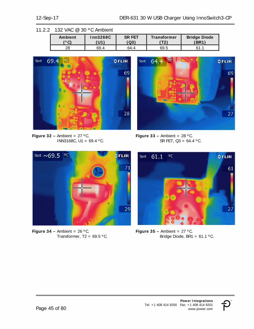
132 VAC @ 30 ºC Ambient 11.2.2Ambient
(ºC) Inn3268C
(U1) SR FET (Q3)
Transformer (T2)
Bridge Diode (BR1)
28 69.4 64.4 69.5 61.1
Figure 32 – Ambient = 27 ºC.
INN3168C, U1 = 69.4 ºC. Figure 33 – Ambient = 28 ºC.
SR FET, Q3 = 64.4 ºC.
Figure 34 – Ambient = 26 ºC.
Transformer, T2 = 69.5 ºC. Figure 35 – Ambient = 27 ºC.
Bridge Diode, BR1 = 61.1 ºC.
DER-631 30 W USB Charger Using InnoSwitch3-CP 12-Sep-17
Page 46 of 80
Power Integrations, Inc. Tel: +1 408 414 9200 Fax: +1 408 414 9201 www.power.com
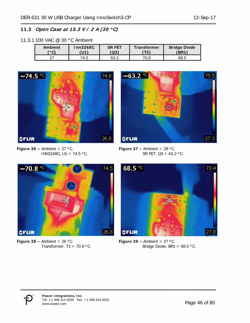
Open Case at 15.3 V / 2 A (30 ºC) 11.3
100 VAC @ 30 ºC Ambient 11.3.1Ambient
(ºC) Inn3268C
(U1) SR FET (Q3)
Transformer (T2)
Bridge Diode (BR1)
27 74.5 63.2 70.8 68.5
Figure 36 – Ambient = 27 ºC.
INN3168C, U1 = 74.5 ºC. Figure 37 – Ambient = 28 ºC.
SR FET, Q3 = 63.2 ºC.
Figure 38 – Ambient = 26 ºC.
Transformer, T2 = 70.8 ºC. Figure 39 – Ambient = 27 ºC.
Bridge Diode, BR1 = 68.5 ºC.

12-Sep-17 DER-631 30 W USB Charger Using InnoSwitch3-CP
Page 47 of 80
Power Integrations Tel: +1 408 414 9200 Fax: +1 408 414 9201
www.power.com
132 VAC @ 30 ºC Ambient 11.3.2Ambient
(ºC) INN3268C
(U1) SR MOSFET
(Q3) Transformer
(T2) Bridge Diode
(BR1) 27 73.4 63.6 68.2 62.2
Figure 40 – Ambient = 27 ºC.
Inn3168C, U1 = 73.4 ºC. Figure 41 – Ambient = 28 ºC.
SR FET, Q3 = 63.6 ºC.
Figure 42 – Ambient = 26 ºC.
Transformer, T2 = 68.2 ºC. Figure 43 – Ambient = 27 ºC.
Bridge Diode, BR1 = 62.2 ºC.
DER-631 30 W USB Charger Using InnoSwitch3-CP 12-Sep-17
Page 48 of 80
Power Integrations, Inc. Tel: +1 408 414 9200 Fax: +1 408 414 9201 www.power.com
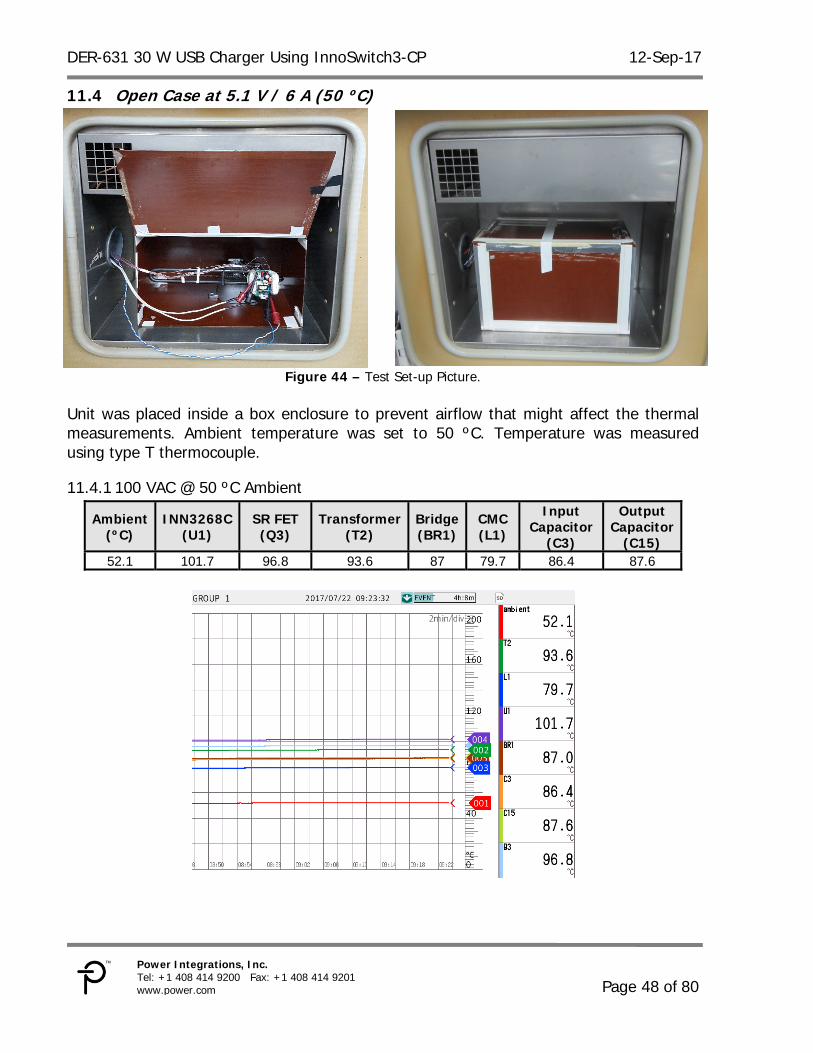
Open Case at 5.1 V / 6 A (50 ºC) 11.4
Figure 44 – Test Set-up Picture.
Unit was placed inside a box enclosure to prevent airflow that might affect the thermal measurements. Ambient temperature was set to 50 ºC. Temperature was measured using type T thermocouple.
100 VAC @ 50 ºC Ambient 11.4.1
Ambient (ºC)
INN3268C (U1)
SR FET (Q3)
Transformer (T2)
Bridge (BR1)
CMC (L1)
Input Capacitor
(C3)
Output Capacitor
(C15) 52.1 101.7 96.8 93.6 87 79.7 86.4 87.6
12-Sep-17 DER-631 30 W USB Charger Using InnoSwitch3-CP
Page 49 of 80
Power Integrations Tel: +1 408 414 9200 Fax: +1 408 414 9201
www.power.com
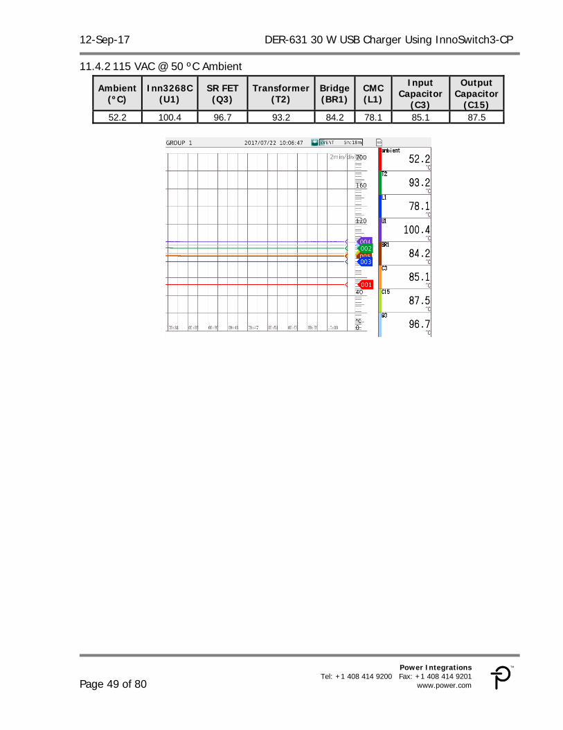
115 VAC @ 50 ºC Ambient 11.4.2
Ambient (ºC)
Inn3268C (U1)
SR FET (Q3)
Transformer (T2)
Bridge (BR1)
CMC (L1)
Input Capacitor
(C3)
Output Capacitor
(C15) 52.2 100.4 96.7 93.2 84.2 78.1 85.1 87.5
DER-631 30 W USB Charger Using InnoSwitch3-CP 12-Sep-17
Page 50 of 80
Power Integrations, Inc. Tel: +1 408 414 9200 Fax: +1 408 414 9201 www.power.com
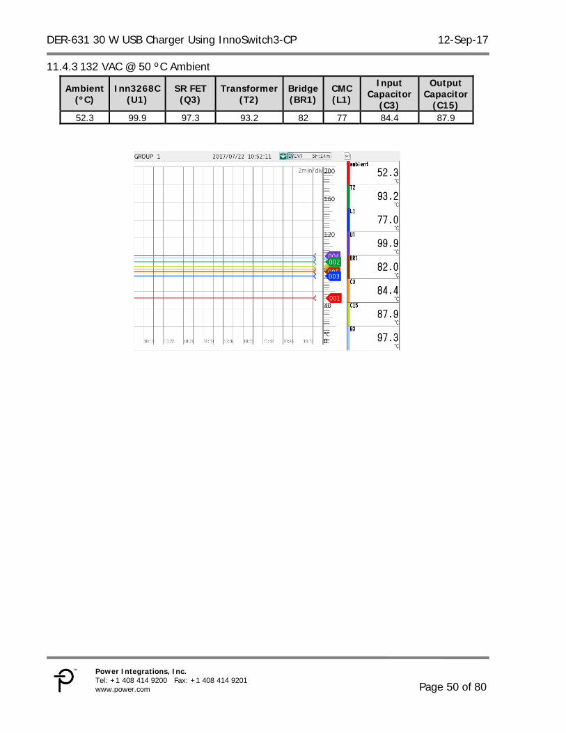
132 VAC @ 50 ºC Ambient 11.4.3
Ambient (ºC)
Inn3268C (U1)
SR FET (Q3)
Transformer (T2)
Bridge (BR1)
CMC (L1)
Input Capacitor
(C3)
Output Capacitor
(C15) 52.3 99.9 97.3 93.2 82 77 84.4 87.9

12-Sep-17 DER-631 30 W USB Charger Using InnoSwitch3-CP
Page 51 of 80
Power Integrations Tel: +1 408 414 9200 Fax: +1 408 414 9201
www.power.com
Open Case at 9.2 V / 3.3 A (50 ºC) 11.5
100 VAC @ 50 ºC Ambient 11.5.1
Ambient (ºC)
Inn3268C (U1)
SR FET (Q3)
Transformer (T2)
Bridge (BR1)
CMC (L1)
Input Capacitor
(C3)
Output Capacitor
(C15) 51.9 89.4 81.9 85.2 82.9 75.1 80.5 75.2
DER-631 30 W USB Charger Using InnoSwitch3-CP 12-Sep-17
Page 52 of 80
Power Integrations, Inc. Tel: +1 408 414 9200 Fax: +1 408 414 9201 www.power.com
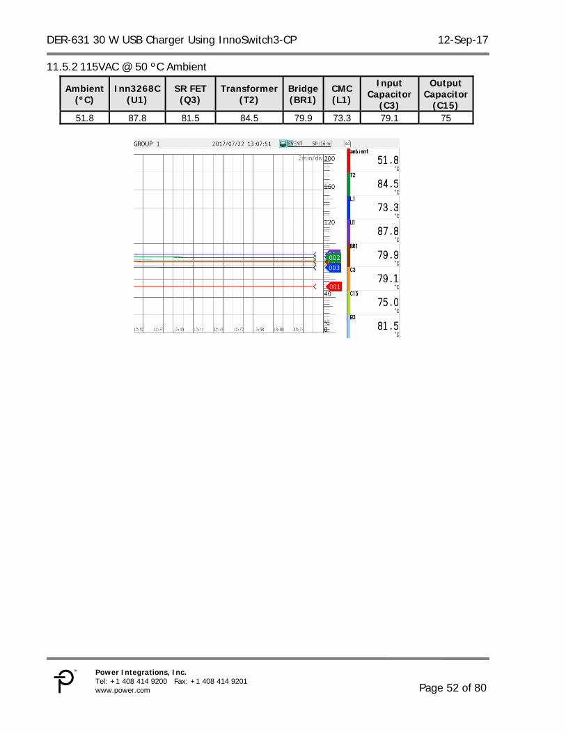
115VAC @ 50 ºC Ambient 11.5.2
Ambient (ºC)
Inn3268C (U1)
SR FET (Q3)
Transformer (T2)
Bridge (BR1)
CMC (L1)
Input Capacitor
(C3)
Output Capacitor
(C15) 51.8 87.8 81.5 84.5 79.9 73.3 79.1 75
12-Sep-17 DER-631 30 W USB Charger Using InnoSwitch3-CP
Page 53 of 80
Power Integrations Tel: +1 408 414 9200 Fax: +1 408 414 9201
www.power.com
132 VAC @ 50 ºC Ambient 11.5.3
Ambient (ºC)
Inn3268C (U1)
SR FET (Q3)
Transformer (T2)
Bridge (BR1)
CMC (L1)
Input Capacitor
(C3)
Output Capacitor
(C15) 51.8 87.0 81.5 84.2 77.6 72 78.2 75

DER-631 30 W USB Charger Using InnoSwitch3-CP 12-Sep-17
Page 54 of 80
Power Integrations, Inc. Tel: +1 408 414 9200 Fax: +1 408 414 9201 www.power.com
Open Case at 15.3 V / 2 A (50°C) 11.6
100 VAC @ 50 ºC Ambient 11.6.1
Ambient (ºC)
Inn3268C (U1)
SR FET (Q3)
Transformer (T2)
Bridge (BR1)
CMC (L1)
Input Capacitor
(C3)
Output Capacitor
(C15) 51.8 91.4 79.1 85.1 84.1 76.1 82 71.7
12-Sep-17 DER-631 30 W USB Charger Using InnoSwitch3-CP
Page 55 of 80
Power Integrations Tel: +1 408 414 9200 Fax: +1 408 414 9201
www.power.com
115 VAC @ 50 ºC Ambient 11.6.2
Ambient (ºC)
Inn3268C (U1)
SR FET (Q3)
Transformer (T2)
Bridge (BR1)
CMC (L1)
Input Capacitor
(C3)
Output Capacitor
(C15) 50 89.7 78.7 84.4 81 74.2 80.6 71.5
DER-631 30 W USB Charger Using InnoSwitch3-CP 12-Sep-17
Page 56 of 80
Power Integrations, Inc. Tel: +1 408 414 9200 Fax: +1 408 414 9201 www.power.com
132 VAC @ 50 ºC Ambient 11.6.3
Ambient (ºC)
INN3268C (U1)
SR MOSFET
(Q3)
Transformer (T2)
Bridge (BR1)
CMC (L1)
Input Capacitor
(C3)
Output Capacitor
(C15) 50 88.7 78.6 84.1 78.6 72.9 79.6 71.4
12-Sep-17 DER-631 30 W USB Charger Using InnoSwitch3-CP
Page 57 of 80
Power Integrations Tel: +1 408 414 9200 Fax: +1 408 414 9201
www.power.com
Waveforms 12
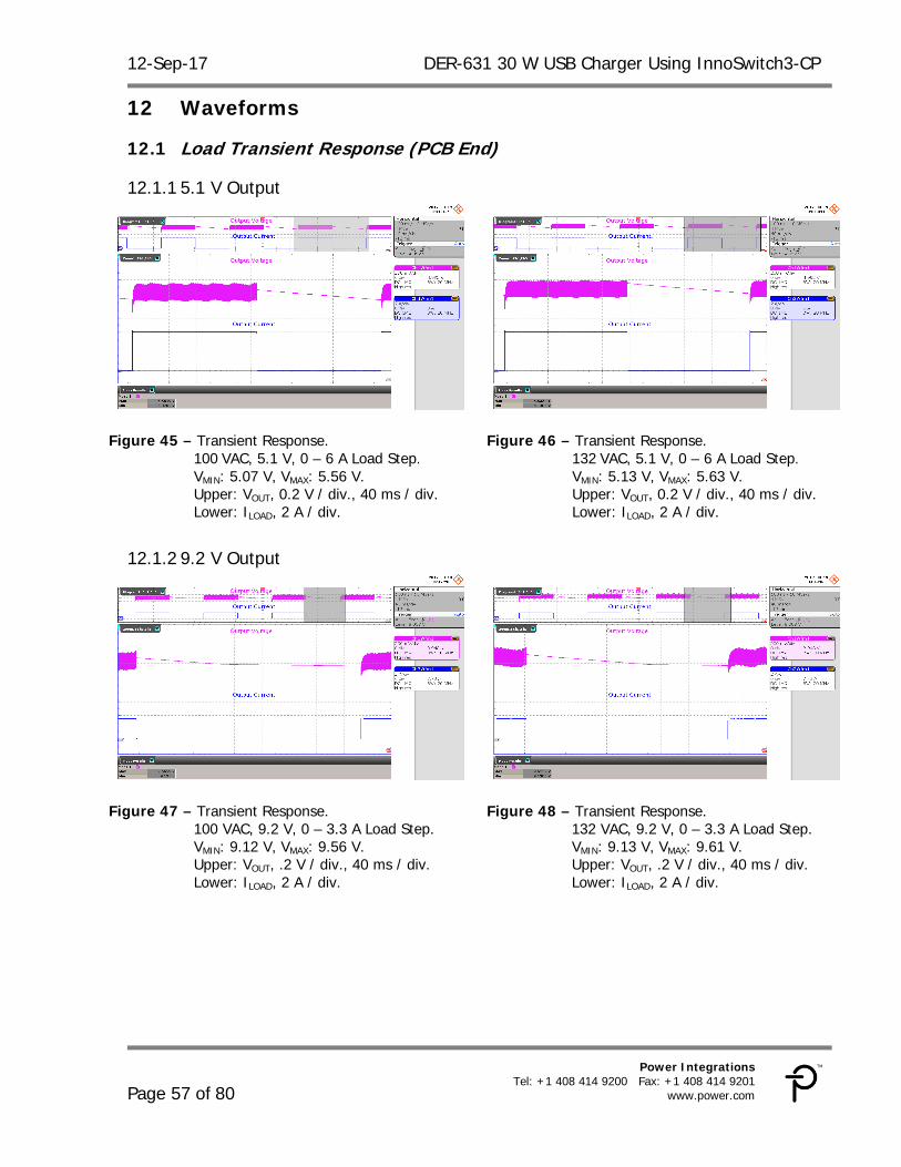
Load Transient Response (PCB End) 12.1
5.1 V Output 12.1.1
Figure 45 – Transient Response.
100VAC, 5.1 V, 0 – 6 A Load Step. VMIN: 5.07 V, VMAX: 5.56 V. Upper: VOUT, 0.2 V / div., 40 ms / div. Lower: ILOAD, 2 A / div.
Figure 46 – Transient Response. 132VAC, 5.1 V, 0 – 6 A Load Step. VMIN: 5.13 V, VMAX: 5.63 V. Upper: VOUT, 0.2 V / div., 40 ms / div. Lower: ILOAD, 2 A / div.
9.2 V Output 12.1.2
Figure 47 – Transient Response.
100 VAC, 9.2 V, 0 – 3.3 A Load Step. VMIN: 9.12 V, VMAX: 9.56 V. Upper: VOUT, .2 V / div., 40 ms / div. Lower: ILOAD, 2 A / div.
Figure 48 – Transient Response. 132 VAC, 9.2 V, 0 – 3.3 A Load Step. VMIN: 9.13 V, VMAX: 9.61 V. Upper: VOUT, .2 V / div., 40 ms / div. Lower: ILOAD, 2 A / div.
DER-631 30 W USB Charger Using InnoSwitch3-CP 12-Sep-17
Page 58 of 80
Power Integrations, Inc. Tel: +1 408 414 9200 Fax: +1 408 414 9201 www.power.com
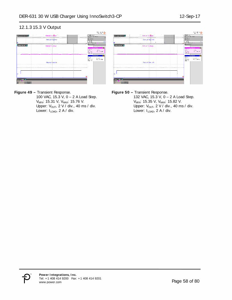
15.3 V Output 12.1.3
Figure 49 – Transient Response.
100 VAC, 15.3 V, 0 – 2 A Load Step. VMIN: 15.31 V, VMAX: 15.76 V. Upper: VOUT, 2 V / div., 40 ms / div. Lower: ILOAD, 2 A / div.
Figure 50 – Transient Response. 132 VAC, 15.3 V, 0 – 2 A Load Step. VMIN: 15.35 V, VMAX: 15.82 V. Upper: VOUT, 2 V / div., 40 ms / div. Lower: ILOAD, 2 A / div.
12-Sep-17 DER-631 30 W USB Charger Using InnoSwitch3-CP
Page 59 of 80
Power Integrations Tel: +1 408 414 9200 Fax: +1 408 414 9201
www.power.com
Switching Waveforms 12.2
Drain Voltage and Current (Normal Operation) 12.2.1
5 V Output 12.2.1.1
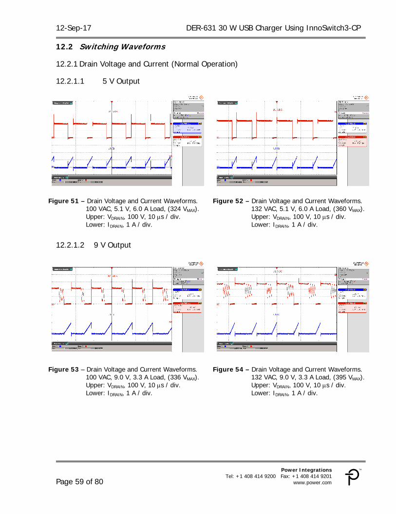
Figure 51 – Drain Voltage and Current Waveforms.
100 VAC, 5.1 V, 6.0 A Load, (324 VMAX). Upper: VDRAIN, 100 V, 10 s / div. Lower: IDRAIN, 1 A / div.
Figure 52 – Drain Voltage and Current Waveforms. 132 VAC, 5.1 V, 6.0 A Load, (360 VMAX). Upper: VDRAIN, 100 V, 10 s / div. Lower: IDRAIN, 1 A / div.
9 V Output 12.2.1.2
Figure 53 – Drain Voltage and Current Waveforms. 100 VAC, 9.0 V, 3.3 A Load, (336 VMAX). Upper: VDRAIN, 100 V, 10 s / div. Lower: IDRAIN, 1 A / div.
Figure 54 – Drain Voltage and Current Waveforms. 132 VAC, 9.0 V, 3.3 A Load, (395 VMAX). Upper: VDRAIN, 100 V, 10 s / div. Lower: IDRAIN, 1 A / div.
DER-631 30 W USB Charger Using InnoSwitch3-CP 12-Sep-17
Page 60 of 80
Power Integrations, Inc. Tel: +1 408 414 9200 Fax: +1 408 414 9201 www.power.com
15 V Output 12.2.1.3
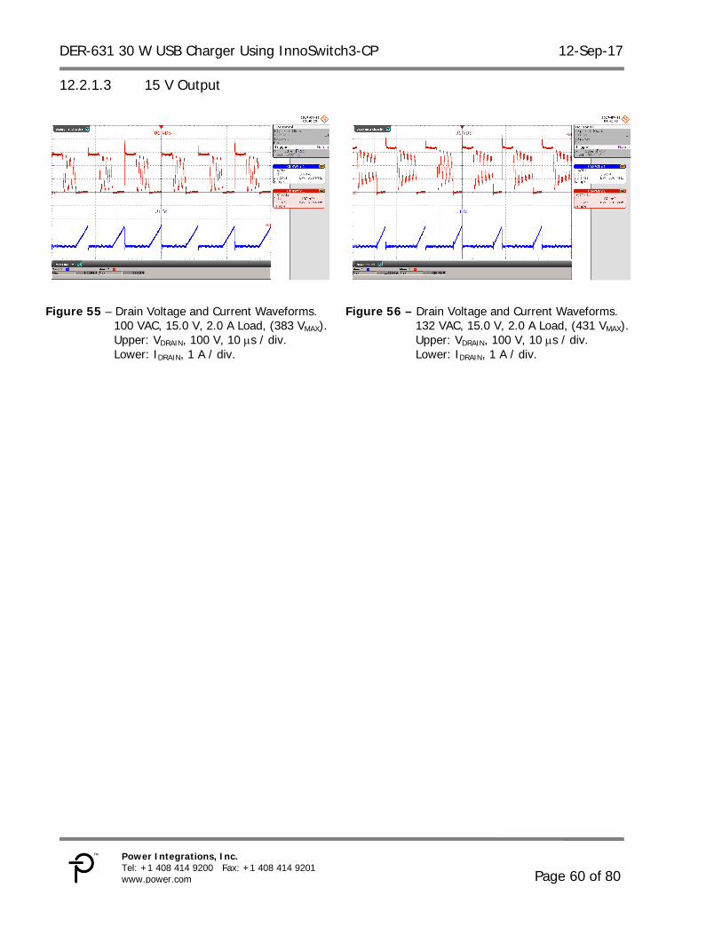
Figure 55 – Drain Voltage and Current Waveforms. 100 VAC, 15.0 V, 2.0 A Load, (383 VMAX). Upper: VDRAIN, 100 V, 10 s / div. Lower: IDRAIN, 1 A / div.
Figure 56 – Drain Voltage and Current Waveforms. 132 VAC, 15.0 V, 2.0 A Load, (431 VMAX). Upper: VDRAIN, 100 V, 10 s / div. Lower: IDRAIN, 1 A / div.
12-Sep-17 DER-631 30 W USB Charger Using InnoSwitch3-CP
Page 61 of 80
Power Integrations Tel: +1 408 414 9200 Fax: +1 408 414 9201
www.power.com
Drain Voltage and Current (Start-up) 12.2.2
5 V Output 12.2.2.1
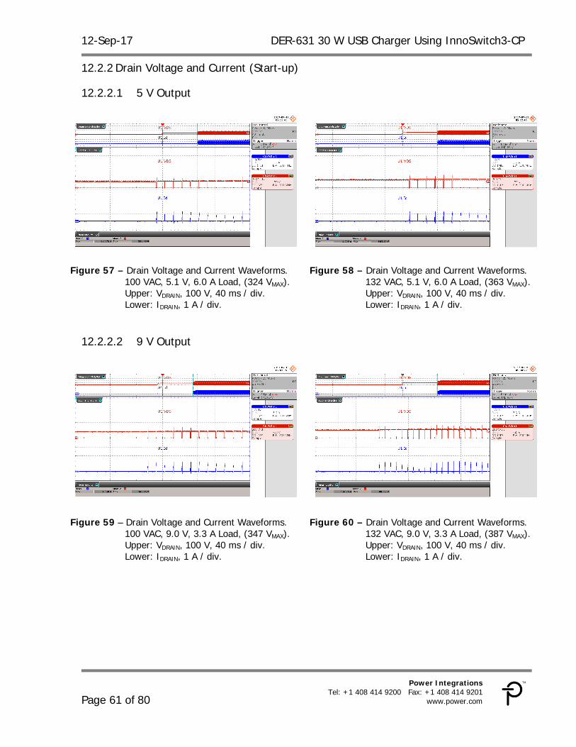
Figure 57 – Drain Voltage and Current Waveforms. 100 VAC, 5.1 V, 6.0 A Load, (324 VMAX). Upper: VDRAIN, 100 V, 40 ms / div. Lower: IDRAIN, 1 A / div.
Figure 58 – Drain Voltage and Current Waveforms. 132 VAC, 5.1 V, 6.0 A Load, (363 VMAX). Upper: VDRAIN, 100 V, 40 ms / div. Lower: IDRAIN, 1 A / div.
9 V Output 12.2.2.2
Figure 59 – Drain Voltage and Current Waveforms. 100 VAC, 9.0 V, 3.3 A Load, (347 VMAX). Upper: VDRAIN, 100 V, 40 ms / div. Lower: IDRAIN, 1 A / div.
Figure 60 – Drain Voltage and Current Waveforms. 132 VAC, 9.0 V, 3.3 A Load, (387 VMAX). Upper: VDRAIN, 100 V, 40 ms / div. Lower: IDRAIN, 1 A / div.

DER-631 30 W USB Charger Using InnoSwitch3-CP 12-Sep-17
Page 62 of 80
Power Integrations, Inc. Tel: +1 408 414 9200 Fax: +1 408 414 9201 www.power.com
15 V Output 12.2.2.3
Figure 61 – Drain Voltage and Current Waveforms. 100 VAC, 15.0 V, 2.0 A Load, (387 VMAX). Upper: VDRAIN, 100 V, 40 ms / div. Lower: IDRAIN, 1 A / div.
Figure 62 – Drain Voltage and Current Waveforms. 132 VAC, 15.0 V, 2.0 A Load, (434 VMAX). Upper: VDRAIN, 100 V, 40 ms / div. Lower: IDRAIN, 1 A / div.

12-Sep-17 DER-631 30 W USB Charger Using InnoSwitch3-CP
Page 63 of 80
Power Integrations Tel: +1 408 414 9200 Fax: +1 408 414 9201
www.power.com
SR MOSFET Voltage 12.2.3
5 V Output 12.2.3.1
Figure 63 – SR FET Voltage Waveform.
100 VAC, 5.1 V, 6.0 A Load, (38.9 VMAX). VDRAIN, 10 V, 10 s / div.
Figure 64 – SR FET Voltage Waveform. 132 VAC, 5.1 V, 6.0 A Load, (50.1 VMAX). VDRAIN, 10 V, 10 s / div.
9 V Output 12.2.3.2
Figure 65 – SR1 FET Voltage Waveform.
100 VAC, 9.0 V, 3.3 A Load, (29.5 VMAX). VDRAIN, 10 V, 10 s / div.
Figure 66 – SR1 FET Voltage Waveform. 132 VAC, 9.0 V, 3.3 A Load, (39.7 VMAX). VDRAIN, 10 V, 10 s / div.

DER-631 30 W USB Charger Using InnoSwitch3-CP 12-Sep-17
Page 64 of 80
Power Integrations, Inc. Tel: +1 408 414 9200 Fax: +1 408 414 9201 www.power.com
15 V Output 12.2.3.3
Figure 67 – SR FET Voltage Waveform.
100 VAC, 15.0 V, 2.0 A Load, (35.4 VMAX). VDRAIN, 10 V, 10 s / div.
Figure 68 – SR FET Voltage Waveform. 132 VAC, 15.0 V, 2.0 A Load, (46.1 VMAX). VDRAIN, 10 V, 10 s / div.
12-Sep-17 DER-631 30 W USB Charger Using InnoSwitch3-CP
Page 65 of 80
Power Integrations Tel: +1 408 414 9200 Fax: +1 408 414 9201
www.power.com
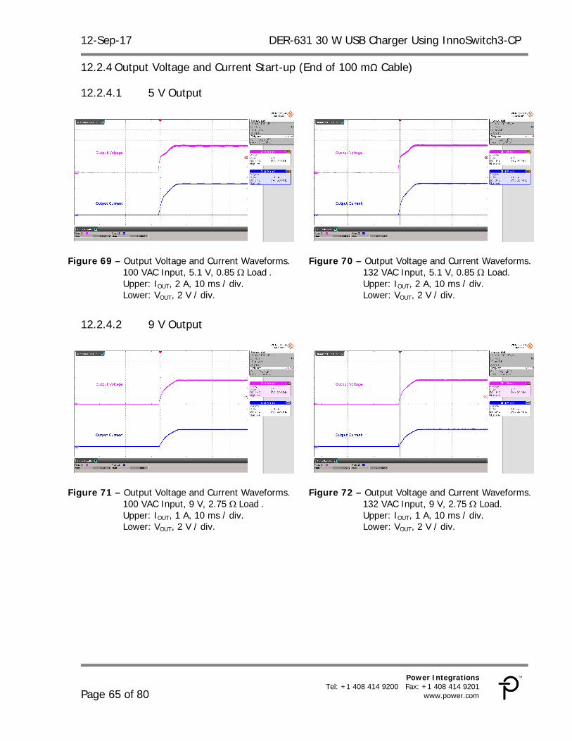
Output Voltage and Current Start-up (End of 100 mΩ Cable) 12.2.4
5 V Output 12.2.4.1
Figure 69 – Output Voltage and Current Waveforms.
100 VAC Input, 5.1 V, 0.85 Load. Upper: IOUT, 2 A, 10 ms / div. Lower: VOUT, 2 V / div.
Figure 70 – Output Voltage and Current Waveforms. 132 VAC Input, 5.1 V, 0.85 Load. Upper: IOUT, 2 A, 10 ms / div. Lower: VOUT, 2 V / div.
9 V Output 12.2.4.2
Figure 71 – Output Voltage and Current Waveforms.
100 VAC Input, 9 V, 2.75 Load. Upper: IOUT, 1 A, 10 ms / div. Lower: VOUT, 2 V / div.
Figure 72 – Output Voltage and Current Waveforms. 132 VAC Input, 9 V, 2.75 Load. Upper: IOUT, 1 A, 10 ms / div. Lower: VOUT, 2 V / div.
DER-631 30 W USB Charger Using InnoSwitch3-CP 12-Sep-17
Page 66 of 80
Power Integrations, Inc. Tel: +1 408 414 9200 Fax: +1 408 414 9201 www.power.com
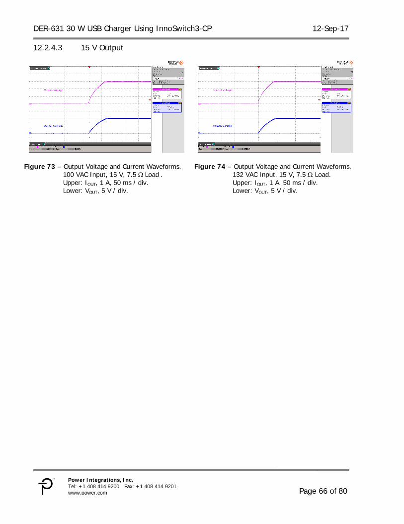
15 V Output 12.2.4.3
Figure 73 – Output Voltage and Current Waveforms.
100 VAC Input, 15 V, 7.5 Load. Upper: IOUT, 1 A, 50 ms / div. Lower: VOUT, 5 V / div.
Figure 74 – Output Voltage and Current Waveforms. 132 VAC Input, 15 V, 7.5 Load. Upper: IOUT, 1 A, 50 ms / div. Lower: VOUT, 5 V / div.

12-Sep-17 DER-631 30 W USB Charger Using InnoSwitch3-CP
Page 67 of 80
Power Integrations Tel: +1 408 414 9200 Fax: +1 408 414 9201
www.power.com
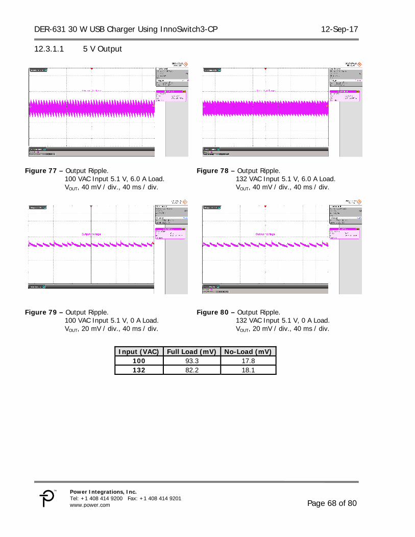
Output Ripple Measurements 12.3
Ripple Measurement Technique 12.3.1For DC output ripple measurements, a modified oscilloscope test probe must be utilized in order to reduce spurious signals due to pick-up. Details of the probe modification are provided in the Figures below. The 4987BA probe adapter is affixed with two capacitors tied in parallel across the probe tip. The capacitors include one (1) 0.1 F/50 V ceramic type and one (1) 47 F/50 V aluminum electrolytic. The aluminum electrolytic type capacitor is polarized, so proper polarity across DC outputs must be maintained (see below). Ripple measurement done at the end of a 100m cable.
Figure 75 – Oscilloscope Probe Prepared for Ripple Measurement. (End Cap and Ground Lead Removed)
Figure 76 – Oscilloscope Probe with Probe Master (www.probemaster.com) 4987A BNC Adapter.
(Modified with wires for ripple measurement, and two parallel decoupling capacitors added)
Probe Ground
Probe Tip
DER-631 30 W USB Charger Using InnoSwitch3-CP 12-Sep-17
Page 68 of 80
Power Integrations, Inc. Tel: +1 408 414 9200 Fax: +1 408 414 9201 www.power.com
5 V Output 12.3.1.1
Figure 77 – Output Ripple.
100 VAC Input 5.1 V, 6.0 A Load. VOUT, 40 mV / div., 40 ms / div.
Figure 78 – Output Ripple. 132 VAC Input 5.1 V, 6.0 A Load. VOUT, 40 mV / div., 40 ms / div.
Figure 79 – Output Ripple. 100 VAC Input 5.1 V, 0 A Load. VOUT, 20 mV / div., 40 ms / div.
Figure 80 – Output Ripple. 132 VAC Input 5.1 V, 0 A Load. VOUT, 20 mV / div., 40 ms / div.
Input (VAC) Full Load (mV) No-Load (mV)
100 93.3 17.8 132 82.2 18.1
12-Sep-17 DER-631 30 W USB Charger Using InnoSwitch3-CP
Page 69 of 80
Power Integrations Tel: +1 408 414 9200 Fax: +1 408 414 9201
www.power.com
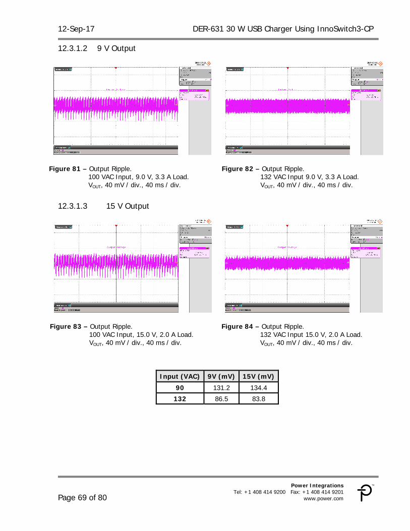
9 V Output 12.3.1.2
Figure 81 – Output Ripple.
100 VAC Input, 9.0 V, 3.3 A Load. VOUT, 40 mV / div., 40 ms / div.
Figure 82 – Output Ripple. 132 VAC Input 9.0 V, 3.3 A Load. VOUT, 40 mV / div., 40 ms / div.
15 V Output 12.3.1.3
Figure 83 – Output Ripple.
100 VAC Input, 15.0 V, 2.0 A Load. VOUT, 40 mV / div., 40 ms / div.
Figure 84 – Output Ripple. 132 VAC Input 15.0 V, 2.0 A Load. VOUT, 40 mV / div., 40 ms / div.
Input (VAC) 9V (mV) 15V (mV)
90 131.2 134.4
132 86.5 83.8

DER-631 30 W USB Charger Using InnoSwitch3-CP 12-Sep-17
Page 70 of 80
Power Integrations, Inc. Tel: +1 408 414 9200 Fax: +1 408 414 9201 www.power.com
Conducted EMI 13
Test Set-up 13.1
Equipment and Load Used 13.1.11. Rohde and Schwarz ENV216 two line V-network. 2. Rohde and Schwarz ESRP EMI test receiver. 3. Hioki 3322 power hitester. 4. Chroma measurement test fixture, model A662003. 5. Resistor load with input voltage set at 115 VAC.
Figure 85 – Conducted EMI Test Set-up.
12-Sep-17 DER-631 30 W USB Charger Using InnoSwitch3-CP
Page 71 of 80
Power Integrations Tel: +1 408 414 9200 Fax: +1 408 414 9201
www.power.com
EMI Test Result 13.2
Floating Output 13.2.1
Output 5.1 V / 6 A 13.2.1.1
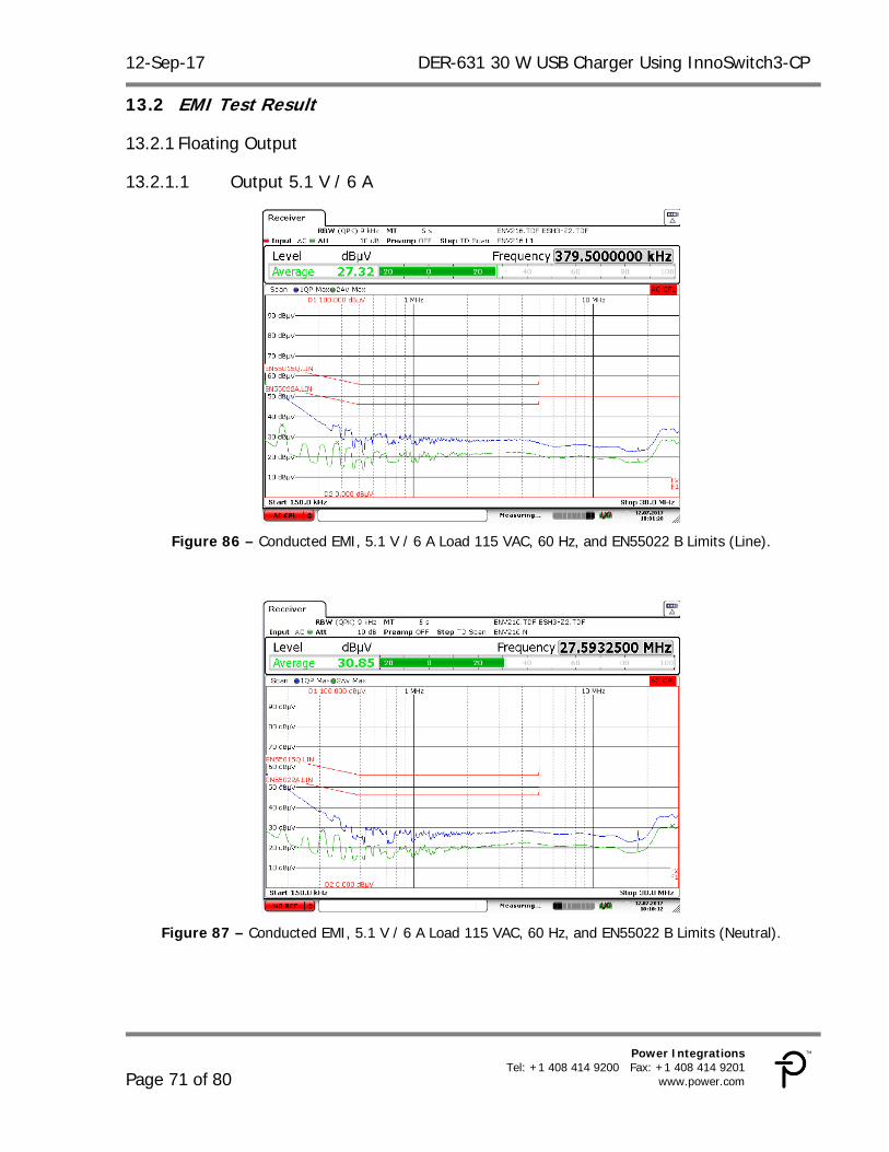
Figure 86 – Conducted EMI, 5.1 V / 6 A Load 115 VAC, 60 Hz, and EN55022 B Limits (Line).
Figure 87 – Conducted EMI, 5.1 V / 6 A Load 115 VAC, 60 Hz, and EN55022 B Limits (Neutral).

DER-631 30 W USB Charger Using InnoSwitch3-CP 12-Sep-17
Page 72 of 80
Power Integrations, Inc. Tel: +1 408 414 9200 Fax: +1 408 414 9201 www.power.com
Output 9 V / 3.3 A 13.2.1.2
Figure 88 – Conducted EMI, 9 V / 3.3 A Load 115 VAC, 60 Hz, and EN55022 B Limits (Line).
Figure 89 – Conducted EMI, 9 V / 3.3 A Load 115 VAC, 60 Hz, and EN55022 B Limits (Neutral).
12-Sep-17 DER-631 30 W USB Charger Using InnoSwitch3-CP
Page 73 of 80
Power Integrations Tel: +1 408 414 9200 Fax: +1 408 414 9201
www.power.com
Output 15 V / 2 A 13.2.1.3
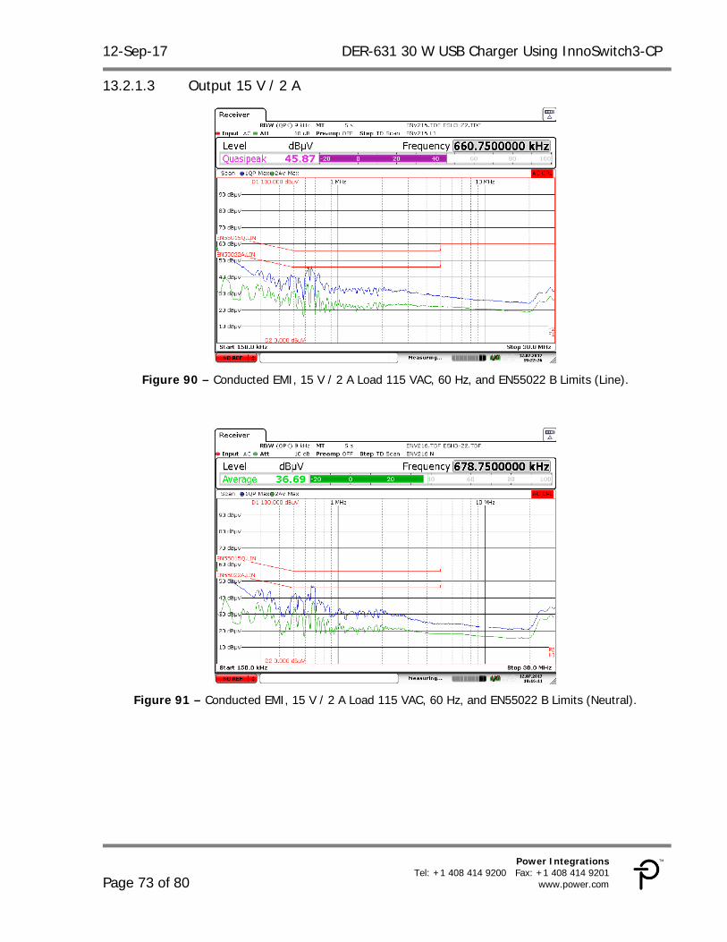
Figure 90 – Conducted EMI, 15 V / 2 A Load 115 VAC, 60 Hz, and EN55022 B Limits (Line).
Figure 91 – Conducted EMI, 15 V / 2 A Load 115 VAC, 60 Hz, and EN55022 B Limits (Neutral).
DER-631 30 W USB Charger Using InnoSwitch3-CP 12-Sep-17
Page 74 of 80
Power Integrations, Inc. Tel: +1 408 414 9200 Fax: +1 408 414 9201 www.power.com
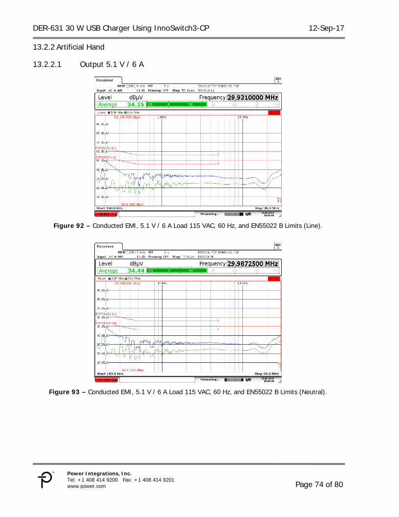
Artificial Hand 13.2.2
Output 5.1 V / 6 A 13.2.2.1
Figure 92 – Conducted EMI, 5.1 V / 6 A Load 115 VAC, 60 Hz, and EN55022 B Limits (Line).
Figure 93 – Conducted EMI, 5.1 V / 6 A Load 115 VAC, 60 Hz, and EN55022 B Limits (Neutral).
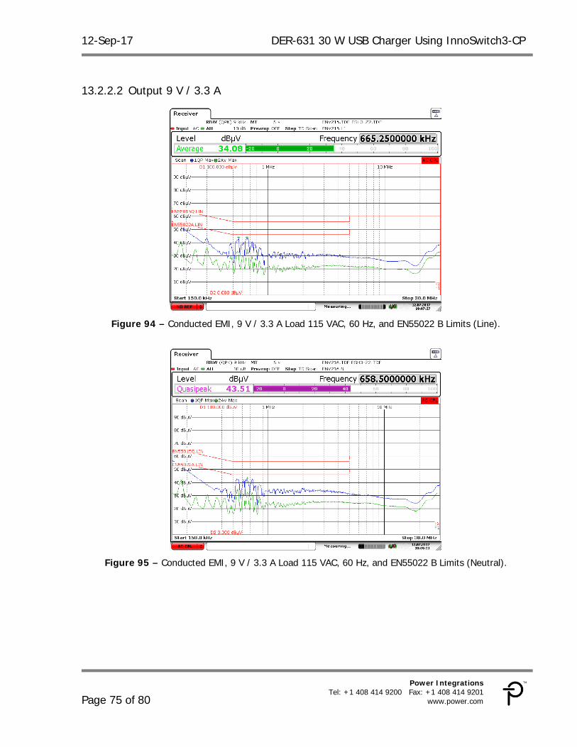
12-Sep-17 DER-631 30 W USB Charger Using InnoSwitch3-CP
Page 75 of 80
Power Integrations Tel: +1 408 414 9200 Fax: +1 408 414 9201
www.power.com
Output 9 V / 3.3 A 13.2.2.2
Figure 94 – Conducted EMI, 9 V / 3.3 A Load 115 VAC, 60 Hz, and EN55022 B Limits (Line).
Figure 95 – Conducted EMI, 9 V / 3.3 A Load 115 VAC, 60 Hz, and EN55022 B Limits (Neutral).
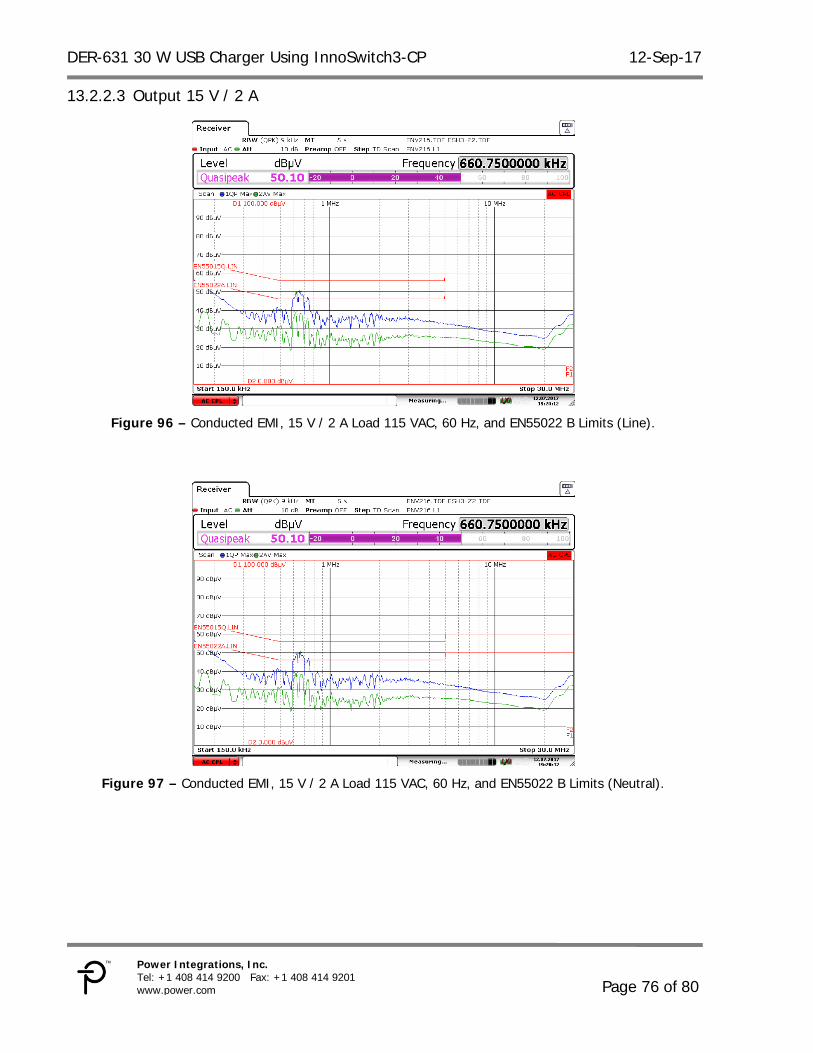
DER-631 30 W USB Charger Using InnoSwitch3-CP 12-Sep-17
Page 76 of 80
Power Integrations, Inc. Tel: +1 408 414 9200 Fax: +1 408 414 9201 www.power.com
Output 15 V / 2 A 13.2.2.3
Figure 96 – Conducted EMI, 15 V / 2 A Load 115 VAC, 60 Hz, and EN55022 B Limits (Line).
Figure 97 – Conducted EMI, 15 V / 2 A Load 115 VAC, 60 Hz, and EN55022 B Limits (Neutral).

12-Sep-17 DER-631 30 W USB Charger Using InnoSwitch3-CP
Page 77 of 80
Power Integrations Tel: +1 408 414 9200 Fax: +1 408 414 9201
www.power.com
Line Surge 14The unit was subjected to ±2000 V, common mode surge and ±1000 V differential surge using 10 strikes at each condition. A test failure was defined as a non-recoverable interruption of output requiring repair or recycling of input voltage.
Surge Level (V)
Input Voltage (VAC)
Injection Location
Injection Phase
(°)
Test Result (Pass/Fail)
+1000 115 L to N 0 Pass -1000 115 L to N 0 Pass +1000 115 L to N 90 Pass -1000 115 L to N 90 Pass +2000 115 L to PE 0 Pass -2000 115 L to PE 0 Pass +2000 115 L to PE 90 Pass -2000 115 L to PE 90 Pass
Note: Output ground of output connected to PE.
Figure 98 – U1 Drain to Source Voltage, 15 V / 2 A Load 115 VAC, 60 Hz, and Line Input Surge Test.

DER-631 30 W USB Charger Using InnoSwitch3-CP 12-Sep-17
Page 78 of 80
Power Integrations, Inc. Tel: +1 408 414 9200 Fax: +1 408 414 9201 www.power.com
ESD Test 15Passed ±8 kV contact test.
Contact Voltage (kV) Applied to Number
of Strikes Test Result
8 5 V 10 PASS -8 5 V 10 PASS 8 9 V 10 PASS -8 9 V 10 PASS 8 15 V 10 PASS -8 15 V 10 PASS
Passed ±15 kV air test.
Differential Voltage (kV) Applied to Number
of Strikes Test Result
15 5 V 10 PASS -15 5 V 10 PASS 15 9 V 10 PASS -15 9 V 10 PASS 15 15 V 10 PASS -15 15 V 10 PASS
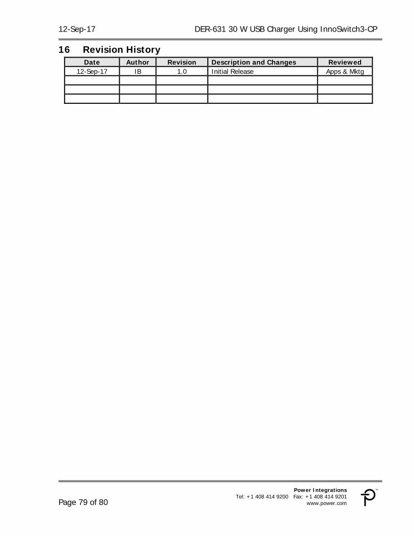
12-Sep-17 DER-631 30 W USB Charger Using InnoSwitch3-CP
Page 79 of 80
Power Integrations Tel: +1 408 414 9200 Fax: +1 408 414 9201
www.power.com
Revision History 16Date Author Revision Description and Changes Reviewed
12-Sep-17 IB 1.0 Initial Release Apps & Mktg

DER-631 30 W USB Charger Using InnoSwitch3-CP 12-Sep-17
Page 80 of 80
Power Integrations, Inc. Tel: +1 408 414 9200 Fax: +1 408 414 9201 www.power.com
For the latest updates, visit our website: www.power.com Reference Designs are technical proposals concerning how to use Power Integrations’ gate drivers in particular applications and/or with certain power modules. These proposals are “as is” and are not subject to any qualification process. The suitability, implementation and qualification are the sole responsibility of the end user. The statements, technical information and recommendations contained herein are believed to be accurate as of the date hereof. All parameters, numbers, values and other technical data included in the technical information were calculated and determined to our best knowledge in accordance with the relevant technical norms (if any). They may base on assumptions or operational conditions that do not necessarily apply in general. We exclude any representation or warranty, express or implied, in relation to the accuracy or completeness of the statements, technical information and recommendations contained herein. No responsibility is accepted for the accuracy or sufficiency of any of the statements, technical information, recommendations or opinions communicated and any liability for any direct, indirect or consequential loss or damage suffered by any person arising therefrom is expressly disclaimed. Power Integrations reserves the right to make changes to its products at any time to improve reliability or manufacturability. Power Integrations does not assume any liability arising from the use of any device or circuit described herein. POWER INTEGRATIONS MAKES NO WARRANTY HEREIN AND SPECIFICALLY DISCLAIMS ALL WARRANTIES INCLUDING, WITHOUT LIMITATION, THE IMPLIED WARRANTIES OF MERCHANTABILITY, FITNESS FOR A PARTICULAR PURPOSE, AND NON-INFRINGEMENT OF THIRD PARTY RIGHTS. Patent Information The products and applications illustrated herein (including transformer construction and circuits’ external to the products) may be covered by one or more U.S. and foreign patents, or potentially by pending U.S. and foreign patent applications assigned to Power
Integrations. A complete list of Power Integrations’ patents may be found at www.power.com. Power Integrations grants its
customers a license under certain patent rights as set forth at http://www.power.com/ip.htm.
The PI Logo, TOPSwitch, TinySwitch, LinkSwitch, LYTSwitch, InnoSwtich, DPA-Switch, PeakSwitch, CAPZero, SENZero, LinkZero, HiperPFS, HiperTFS, HiperLCS, Qspeed, EcoSmart, Clampless, E-Shield, Filterfuse, FluxLink, StackFET, PI Expert and PI FACTS are trademarks of Power Integrations, Inc. Other trademarks are property of their respective companies. ©Copyright 2015 Power Integrations, Inc.
Power Integrations Worldwide Sales Support Locations
WORLD HEADQUARTERS 5245 Hellyer Avenue San Jose, CA 95138, USA. Main: +1-408-414-9200 Customer Service: Phone: +1-408-414-9665 Fax: +1-408-414-9765 e-mail: [email protected]
CHINA (SHANGHAI) Rm 2410, Charity Plaza, No. 88, North Caoxi Road, Shanghai, PRC 200030 Phone: +86-21-6354-6323 Fax: +86-21-6354-6325 e-mail: [email protected]
CHINA (SHENZHEN) 17/F, Hivac Building, No. 2, Keji Nan 8th Road, Nanshan District, Shenzhen, China, 518057 Phone: +86-755-8672-8689 Fax: +86-755-8672-8690 e-mail: [email protected]
GERMANY (AC-DC/LED Sales) Lindwurmstrasse 114 80337, Munich Germany Phone: +49-895-527-39110 Fax: +49-895-527-39200 e-mail: [email protected]
GERMANY (IGBT Driver Sales) HellwegForum 1 59469 Ense, Germany Tel: +49-2938-64-39990 Email: [email protected]
INDIA #1, 14th Main Road Vasanthanagar Bangalore-560052 India Phone: +91-80-4113-8020 Fax: +91-80-4113-8023 e-mail: [email protected]
ITALY Via Milanese 20, 3rd. Fl. 20099 Sesto San Giovanni (MI) Italy Phone: +39-024-550-8701 Fax: +39-028-928-6009 e-mail: [email protected]
JAPAN Kosei Dai-3 Building 2-12-11, Shin-Yokohama, Kohoku-ku, Yokohama-shi, Kanagawa 222-0033 Japan Phone: +81-45-471-1021 Fax: +81-45-471-3717 e-mail: [email protected]
KOREA RM 602, 6FL Korea City Air Terminal B/D, 159-6 Samsung-Dong, Kangnam-Gu, Seoul, 135-728 Korea Phone: +82-2-2016-6610 Fax: +82-2-2016-6630 e-mail: [email protected]
SINGAPORE 51 Newton Road, #19-01/05 Goldhill Plaza Singapore, 308900 Phone: +65-6358-2160 Fax: +65-6358-2015 e-mail: [email protected]
TAIWAN 5F, No. 318, Nei Hu Rd., Sec. 1 Nei Hu District Taipei 11493, Taiwan R.O.C. Phone: +886-2-2659-4570 Fax: +886-2-2659-4550 e-mail: [email protected]
UK Cambridge Semiconductor, a Power Integrations company Westbrook Centre, Block 5, 2nd Floor Milton Road Cambridge CB4 1YG Phone: +44 (0) 1223-446483 e-mail: [email protected]