Design and Optimization of Efficient Wireless Power Transfer Links
97
DESIGN AND OPTIMIZATION OF EFFICIENT WIRELESS POWER TRANSFER LINKS FOR IMPLANTABLE BIOTELEMETRY SYSTEMS (Thesis format: Monograph) by Shawon Senjuti Graduate Program in Electrical and Computer Engineering A thesis submitted in partial fulfillment of the requirements for the degree of Master of Engineering Science The School of Graduate and Postdoctoral Studies The University of Western Ontario London, Ontario, Canada c Shawon Senjuti 2013
Transcript of Design and Optimization of Efficient Wireless Power Transfer Links

DESIGN AND OPTIMIZATION OF EFFICIENT WIRELESS POWERTRANSFER LINKS FOR IMPLANTABLE BIOTELEMETRY SYSTEMS
(Thesis format: Monograph)
by
Shawon Senjuti
Graduate Program in Electrical and Computer Engineering
A thesis submitted in partial fulfillmentof the requirements for the degree of
Master of Engineering Science
The School of Graduate and Postdoctoral StudiesThe University of Western Ontario
London, Ontario, Canada
c© Shawon Senjuti 2013

Abstract
Wireless power transmission is a technique that converts energy from radio frequency (RF)
electromagnetic (EM) waves into DC voltage, which has been used here for the purpose of
providing a power supply to bio–implantable batteryless sensors. The main constraints of the
design are to achieve the minimum power required by the application, by still keeping the
implant size small enough for the living subject’s body. Resonance–based inductive coupling
is a method being actively researched for the use in this type of power transmission, which uses
two pairs of inductor coils in the external and implant circuits.
In this work, we have employed the resonance–based inductive coupling technique in or-
der to develop a design and optimization procedure for the inductors. We have designed two
systems with different configurations, and have achieved power transfer efficiencies of around
80% at a coil distance of 50mm for both systems. We have also optimized the power delivered
to the load (implant) and developed a power harvesting unit. Misalignment issues due to the
subject’s movements have been modeled for calculating the worst–case alignment, and finite
element modeling of the inductors has been performed.
Keywords: biomedical implants, wireless power transfer, inductive coupling, resonance–
based power delivery, power harvesting, coil misalignment, mutual inductance, finite element
method.
ii

Acknowledgments
I would like to express my sincere gratitude to a number of individuals and institutions,
whose generous support has led me to this successful endeavor.
Firstly, I would like to thank Dr. Robert Sobot, my supervisor, for guiding me along the
research process and graciously supporting me throughout the course of the degree.
My thanks also go to my undergraduate instructors at Queen Mary, University of London
for paving my way to becoming an electrical engineer, by enriching my knowledge base with
their expertise and experience.
My gratitude goes to the Electrical and Computer Engineering department at The Uni-
versity of Western Ontario for providing the necessary funding, facilities and a suitable work
environment. I would like to thank all of my industrial sponsors as well as Ontario Graduate
Scholarship (OGS) committee, for partial sponsorship of this degree.
I would also like thank my instructors and my colleagues at the university, for making this
an enriching yet enjoyable journey.
Last but not the least, I give thanks to my parents, for everything they have done for my
education, my husband Rezwan, for his ongoing support that has made this degree possible,
and my son Sameed, for making everything a worthwhile experience.
iii

Contents
Abstract ii
Acknowledgments iii
List of Figures vii
List of Tables ix
List of Abbreviations and Symbols x
1 Introduction 11.1 Review on Inductive Power Transfer Links . . . . . . . . . . . . . . . . . . . . 21.2 Motivation and Research Objectives . . . . . . . . . . . . . . . . . . . . . . . 41.3 Organization of the Thesis . . . . . . . . . . . . . . . . . . . . . . . . . . . . 6
2 Inductor Modeling and Optimization 72.1 Overview . . . . . . . . . . . . . . . . . . . . . . . . . . . . . . . . . . . . . 82.2 Modeling Terms . . . . . . . . . . . . . . . . . . . . . . . . . . . . . . . . . . 9
2.2.1 Mutual Inductance . . . . . . . . . . . . . . . . . . . . . . . . . . . . 92.2.2 Self Inductance . . . . . . . . . . . . . . . . . . . . . . . . . . . . . . 122.2.3 Parasitic Capacitance and SRF . . . . . . . . . . . . . . . . . . . . . . 122.2.4 AC Resistance . . . . . . . . . . . . . . . . . . . . . . . . . . . . . . . 132.2.5 Quality Factor . . . . . . . . . . . . . . . . . . . . . . . . . . . . . . . 15
2.3 Litz Wire and Operating Fequency . . . . . . . . . . . . . . . . . . . . . . . . 162.4 Power Transfer Efficiency . . . . . . . . . . . . . . . . . . . . . . . . . . . . . 162.5 Design Flow and Optimization . . . . . . . . . . . . . . . . . . . . . . . . . . 17
2.5.1 System 1 . . . . . . . . . . . . . . . . . . . . . . . . . . . . . . . . . 212.5.2 System 2 . . . . . . . . . . . . . . . . . . . . . . . . . . . . . . . . . 22
2.6 Results and Analysis . . . . . . . . . . . . . . . . . . . . . . . . . . . . . . . 232.6.1 Quality Factor of Coils . . . . . . . . . . . . . . . . . . . . . . . . . . 242.6.2 Operating Frequency Variation . . . . . . . . . . . . . . . . . . . . . . 252.6.3 Choice of Primary Coil Parameters . . . . . . . . . . . . . . . . . . . . 272.6.4 Two–Coil versus Four–Coil Systems . . . . . . . . . . . . . . . . . . . 28
2.7 Concluding Remarks . . . . . . . . . . . . . . . . . . . . . . . . . . . . . . . 28
3 Power Transfer Circuit 303.1 Resonance–Based Power Transfer . . . . . . . . . . . . . . . . . . . . . . . . 30
iv

3.1.1 Coupled–Mode Theory . . . . . . . . . . . . . . . . . . . . . . . . . . 313.1.2 Reflected Load Theory . . . . . . . . . . . . . . . . . . . . . . . . . . 32
3.2 Circuit Specifications . . . . . . . . . . . . . . . . . . . . . . . . . . . . . . . 323.3 Input and Output Power . . . . . . . . . . . . . . . . . . . . . . . . . . . . . . 34
3.3.1 Effect of Number of Turns on Peak Power . . . . . . . . . . . . . . . . 353.3.2 Effect of Source Resistance . . . . . . . . . . . . . . . . . . . . . . . . 363.3.3 Results . . . . . . . . . . . . . . . . . . . . . . . . . . . . . . . . . . 37
3.4 Power Requirements and Harvesting Unit . . . . . . . . . . . . . . . . . . . . 383.4.1 Charge Pump . . . . . . . . . . . . . . . . . . . . . . . . . . . . . . . 39
3.5 Typical Application Systems . . . . . . . . . . . . . . . . . . . . . . . . . . . 413.6 Summary . . . . . . . . . . . . . . . . . . . . . . . . . . . . . . . . . . . . . 42
4 Misalignment Analysis 444.1 Mutual Inductance with Misalignment . . . . . . . . . . . . . . . . . . . . . . 44
4.1.1 Overview . . . . . . . . . . . . . . . . . . . . . . . . . . . . . . . . . 444.1.2 Cases of Misalignment . . . . . . . . . . . . . . . . . . . . . . . . . . 45
4.2 Techniques for Calculation . . . . . . . . . . . . . . . . . . . . . . . . . . . . 484.3 Results and Discussion . . . . . . . . . . . . . . . . . . . . . . . . . . . . . . 49
4.3.1 Observations and Modeling . . . . . . . . . . . . . . . . . . . . . . . . 524.3.2 Worst–Case Alignment . . . . . . . . . . . . . . . . . . . . . . . . . . 53
4.4 Summary . . . . . . . . . . . . . . . . . . . . . . . . . . . . . . . . . . . . . 56
5 Finite Element Method Modeling and Surrounding Environment of Coils 575.1 Introduction to the Finite Element Method . . . . . . . . . . . . . . . . . . . . 575.2 COMSOL R© 2D Electromagnetic Simulations . . . . . . . . . . . . . . . . . . 59
5.2.1 Model Setup . . . . . . . . . . . . . . . . . . . . . . . . . . . . . . . . 595.2.2 Simulation Results . . . . . . . . . . . . . . . . . . . . . . . . . . . . 615.2.3 Shortcomings of the 2D Axisymmetric . . . . . . . . . . . . . . . . . . 625.2.4 Eigenfrequency . . . . . . . . . . . . . . . . . . . . . . . . . . . . . . 63
5.3 COMSOL R© 3D Electromagnetic Simulations . . . . . . . . . . . . . . . . . . 645.3.1 Model Setup . . . . . . . . . . . . . . . . . . . . . . . . . . . . . . . . 645.3.2 Simulation Results . . . . . . . . . . . . . . . . . . . . . . . . . . . . 655.3.3 Inductance Values . . . . . . . . . . . . . . . . . . . . . . . . . . . . . 665.3.4 Parametric Sweep . . . . . . . . . . . . . . . . . . . . . . . . . . . . . 67
5.4 Standards on RF Radiation and Exposure . . . . . . . . . . . . . . . . . . . . . 675.5 EMPro R© 3D Electromagnetic Simulations . . . . . . . . . . . . . . . . . . . . 69
5.5.1 Model and Simulation Setup . . . . . . . . . . . . . . . . . . . . . . . 715.5.2 Results . . . . . . . . . . . . . . . . . . . . . . . . . . . . . . . . . . 71
5.6 Inclusion of External Structures . . . . . . . . . . . . . . . . . . . . . . . . . . 735.7 Summary . . . . . . . . . . . . . . . . . . . . . . . . . . . . . . . . . . . . . 74
6 Conclusions 766.1 Thesis Contributions . . . . . . . . . . . . . . . . . . . . . . . . . . . . . . . 766.2 Comparison with Previous Works . . . . . . . . . . . . . . . . . . . . . . . . . 786.3 Future Work . . . . . . . . . . . . . . . . . . . . . . . . . . . . . . . . . . . . 79
v

Bibliography 80
Curriculum Vitae 87
vi

List of Figures
1.1 General layout of a wireless and batteryless in vivo bio–sensing microsystemby Cong et.al. [1] c©IEEE 2010 . . . . . . . . . . . . . . . . . . . . . . . . . . 3
1.2 Typical setup of inductively coupled coils (with magnetic field shown). . . . . . 4
2.1 Basic inductor showing current and magnetic field. . . . . . . . . . . . . . . . 82.2 Cross–sectional view of two non–coaxial and non–parallel circular coils. . . . . 112.3 Area efficiency of coil (η) versus coil aspect ratio (h/w). . . . . . . . . . . . . . 142.4 Structure of the inductor coils and Litz wire. . . . . . . . . . . . . . . . . . . . 182.5 The implant PCB boards demonstrating where the inductor is connected. . . . . 192.6 Flowchart of the inductor modeling design flow. . . . . . . . . . . . . . . . . . 202.7 Physical dimensions of the coils (for both systems). . . . . . . . . . . . . . . . 232.8 (a) Efficiency versus unloaded quality factors Q2 and Q3 (Q1 = 1.61, Q4 =
0.06). (b) Efficiency versus loaded quality factors Q1 and Q4 (Q2 = 6422,Q3 = 277, k23 = 0.01). . . . . . . . . . . . . . . . . . . . . . . . . . . . . . . . 24
2.9 Efficiency and output power versus operating frequency (at coil distance=50mm). 252.10 Efficiency versus coil distance and operating frequency. . . . . . . . . . . . . . 262.11 Unloaded Q2 versus operating frequency with different number of layers. . . . . 262.12 Q2 and S RF2 versus number of turns per layer. . . . . . . . . . . . . . . . . . . 272.13 Coil 2 SRF versus number of turns and number of layers. . . . . . . . . . . . . 282.14 PTE versus distance for 2–coil and four–coil systems. . . . . . . . . . . . . . . 29
3.1 Lumped equivalent circuit of the inductor. . . . . . . . . . . . . . . . . . . . . 333.2 Electrical model for the power transfer system. . . . . . . . . . . . . . . . . . . 333.3 (a) 3D plot for PDL versus coil distance and number of turns. (b) 2D plot for
PDL versus coil distance for up to 8 number of turns. . . . . . . . . . . . . . . 353.4 PTE versus coil distance for several number of turns. . . . . . . . . . . . . . . 363.5 PTE versus coil distance for different source resistances. . . . . . . . . . . . . 363.6 Input power, output power, and efficiency of System 1. . . . . . . . . . . . . . 373.7 Input power, output power, and efficiency of System 2. . . . . . . . . . . . . . 373.8 Power harvesting unit with rectifier and voltage regulator blocks. . . . . . . . . 383.9 Output power versus time for different values of Rval. . . . . . . . . . . . . . . 393.10 The charge pump unit. . . . . . . . . . . . . . . . . . . . . . . . . . . . . . . 403.11 Output voltage versus time for different values of Vin. . . . . . . . . . . . . . . 403.12 Block diagram of overall system: external and internal sub–blocks. . . . . . . . 41
4.1 Cross–section of two non–coaxial and non–parallel circular coils, where thesecondary coil is a thin disk coil, represented by a single filamentary coil. . . . 47
vii

4.2 Cross–section of two non–coaxial but parallel circular coils. . . . . . . . . . . . 484.3 Sequence of function calls to perform mutual inductance calculations. . . . . . 494.4 (a) Coupling coefficient k23 versus angular separation θ for different coil dis-
tances c (axial misalignment d is 0). (b) Coupling coefficient k23 versus axialdistance d for different coil distances c (angular misalignment θ is 0). . . . . . . 52
4.5 Sensitivity analysis of k23 with respect to both axial and angular misalignments(c=50mm). . . . . . . . . . . . . . . . . . . . . . . . . . . . . . . . . . . . . . 53
4.6 Flowchart to find worst–case alignment of primary and secondary coils. . . . . 544.7 Typical subject (mouse) with implanted telemetry system powered by external
coil. . . . . . . . . . . . . . . . . . . . . . . . . . . . . . . . . . . . . . . . . 55
5.1 2D coil setup in COMSOL and coarser triangular mesh. . . . . . . . . . . . . 605.2 Magnetic flux density (normal) and electric field (normal). . . . . . . . . . . . 615.3 Coil setup with the secondary coil being misaligned, and its 3D rendition (view
at 225 revolution). . . . . . . . . . . . . . . . . . . . . . . . . . . . . . . . . 625.4 Electric field (normal) at 12.80MHz showing noise. . . . . . . . . . . . . . . . 635.5 3D coil setup in COMSOL and coarse triangular mesh. . . . . . . . . . . . . . 655.6 Electric potential and magnetic flux density (normal). . . . . . . . . . . . . . . 665.7 (a) Mutual inductance versus coil distance. (b) Mutual inductance versus pri-
mary coil radius (coil distance=50mm). (c) Mutual inductance versus axialmisalignment (coil distance=50mm). (d) Mutual inductance versus angularmisalignment (coil distance=50mm). . . . . . . . . . . . . . . . . . . . . . . . 68
5.8 3D coil model in EMPro. . . . . . . . . . . . . . . . . . . . . . . . . . . . . . 705.9 Simulated S-parameters of the EMPro model. . . . . . . . . . . . . . . . . . . 72
viii

List of Tables
2.1 Parameters chart of Litz wire (individual strands) . . . . . . . . . . . . . . . . 162.2 Coils’ physical and electrical specifications: 40 strand AWG44 ( f =850kHz) . . 222.3 Coils’ physical and electrical specifications: 105 strand AWG48 ( f =2.8MHz) . 22
4.1 Detailed sequence of MATLAB functions used in the optimization process(Part 1) . . . . . . . . . . . . . . . . . . . . . . . . . . . . . . . . . . . . . . . 50
4.2 Detailed sequence of MATLAB functions used in the optimization process(Part 2) . . . . . . . . . . . . . . . . . . . . . . . . . . . . . . . . . . . . . . . 51
5.1 Comparison between theoretically calculated and FEM simulated parametervalues . . . . . . . . . . . . . . . . . . . . . . . . . . . . . . . . . . . . . . . 62
6.1 Comparison of this research with other similar works . . . . . . . . . . . . . . 78
ix

List of Abbreviations, Symbols, andNomenclature
WPT Wireless Power TransferICPT Indcutively–Coupled Power Transfer
RF Radio FrequencyEM Electromagnetic
RFID Radio Frequency Identification DevicePTE Power Transfer Efficiency
FEM Finite Element MethodPSC Printed Spiral Coil
IC Integrated CircuitCMOS Complementary Metal–Oxide–Semiconductor
SRF Self–Resonant FrequencyPCB Printed Circuit BoardPDL Power Delivered to the LoadSAR Specific Absorption RatioESR Equivalent Series ResistanceKVL Kirchoff’s Voltage LawRMS Root–Mean–Square
FDTD Finite–Difference Time–DomainDC Direct CurrentAC Alternating Current
IEEE The Institute of Electrical and Electronics EngineersMPE Maximum Permissible ExposurePEC Perfect Electric Conductor
CMT Coupled–Mode TheoryRLT Reflected Load Theory
x

Chapter 1
Introduction
Interest for biomedical implantable devices is gaining momentum among both health profes-
sionals and researchers since they offer a variety of applications. Examples of applications
include automatic drug delivery systems, devices to stimulate specific organs, and monitors
to communicate internal vital signs to the outer world. Though all of these devices perform
different tasks, one of their common issues is that of power requirements, which is a widely
researched area over the past decade.
Genetically engineered laboratory subjects under medical studies are often implanted with
microsensors that are connected by transcutaneous wires. This technique guarantees a constant
power supply and reliable data transmission of the recorded signals, while its main shortcoming
is that it requires the subject to be under anesthesia and, therefore, fails to generate undistorted
life–like physiological data of an untethered freely moving subject [2]. In addition, the size of
the battery that is used as the power source is a limiting factor for the implant’s miniaturization
and lifetime, while the battery itself requires periodical surgical replacement with possible
adverse consequences on the subject such as infections. Hence, a wireless continuous power
delivery system is a more suitable method for providing energy to the implants.
This chapter introduces the topic of the present research work. Section 1.1 provides a com-
prehensive literature review on similar works till date. Section 1.2 presents the motivation
1

Chapter 1. Introduction 2
behind the work and the objectives of the research. Lastly, Section 1.3 describes the organiza-
tional layout of this thesis.
1.1 Review on Inductive Power Transfer Links
The first demonstration of wireless power transfer (WPT) dates back to 1899, performed by
Nikola Tesla in Colorado Springs, Colorado [3]. In his experiment, 200 incandescent lamps
were lightened when powered by a base station 26 miles away. A study on wireless monitoring
systems was conducted in 1957, where development of endoradiosondes or radio–pills was
carried out by [4]. In 1962, a passive echo capsule was also developed for similar purposes
(pressure, temperature and pH sensing) by [5]. Since then several research projects have been
undertaken in this field, including those that have been clinically evaluated, and whose power
requirements vary with device application and can range from tens of microwatts to hundreds
of milliwatts [1], [6].
For implants designed for subjects such as genetically–modified laboratory mice, housing
a battery within the implant would not be possible because of size limitations. The researchers
in [7] have proposed wireless inductively–coupled power transfer (ICPT) solutions for their
telemetry system designed for rats. Their implant uses a rechargeable battery which is charged
when the alignment of the coil enables power transfer, and is discharged when it is misaligned.
Unfortunately, this approach is not suitable for mice since the battery size would be too large
(20mm diameter).
Other energy options would utilize sources from the external environment, such as wind and
solar power, as has been implemented in Smart Dust distributed network devices [8]. However,
human or animal tissues render these methods unsuitable for biomedical implants. Therefore,
a wireless and batteryless approach for power harvesting is achieved with the use of radio
frequency (RF) signals through inductive coupling [9]. Additionally, some studies have shown
how the same link can also be used for data transfer. Although the primary application for

Chapter 1. Introduction 3
Figure 1.1: General layout of a wireless and batteryless in vivo bio–sensing microsystem byCong et.al. [1] c©IEEE 2010
this technique was RF identification (RFID) tags [10], the same principle can be applied to
sensor–based wireless biomedical implants [11].
Some latest research endeavors by [1] in 2009 have developed an implant that has a chip
area of 2.2x2.2mm2 and weighs 130mg and can be integrated with an artery of the mouse for
blood pressure monitoring (Fig. 1.1). The specifications of the chip are ideal for laboratory
mice implants given their arterial diameter of about 200um [12]. Since magnetic coupling
theory enables efficient power transfer only when the magnetic field is perfectly aligned with
the inductor, the challenge is to design a powering system that would work independent of the
subject’s orientation. Such designs, which are mainly focused on the generation of constant
minimum power from the floor of the subject’s cage, have been investigated in [13].
Inductive coupling has been the most popular method for wireless power transfer, which
requires two coils (primary and secondary coils). The efficiency of power transfer between the
coils is a strong function of the coil dimensions and distance between them, which is an unde-
sired trend in the case of freely–moving subjects. Therefore, the recent alternative method of
resonance–based power delivery has been suggested by [14] in 2007 and is explained through
the coupled–mode theory [15]. This multiple–coil based approach is used to decouple adverse

Chapter 1. Introduction 4
External
Circuit
Implant
Circuit
Figure 1.2: Typical setup of inductively coupled coils (with magnetic field shown).
effects of source and load resistance from the coils, and in this way achieve a high quality factor
for them. This method is less sensitive to changes in the coil distance and typically employs
two pairs of coils: one in the external circuit called driver and primary coils, and the other in
the implant itself called secondary and load coils.
Most of the work in this area so far revolves around either static large radii coils for rela-
tively high power transfer applications [14], or printed spiral coils (PSCs) used for low power
integrated circuit (IC) implementations [16]. Some latest studies on wireless power transfer
to implantable devices based on resonance–based inductive coupling with emphasis on their
power transfer link efficiency are presented in [17], [18] and [19].
1.2 Motivation and Research Objectives
The aim of this research is to develop a design and optimization system for implementing
wireless power transmission to small–size biomedical implants for freely–moving subjects.
The system is not application–specific, and thus can be customized and implemented as per
application requirements such as size and power.
The analysis is meant to help future discrete–level WPT system designers to directly achieve
maximum possible power transfer efficiency for their systems by identifying their design con-
straints and application requirements. Therefore, the outline of our research objectives can be

Chapter 1. Introduction 5
defined as follows:
• To be able to completely eliminate the need for batteries in wireless biomedical implants
for small–size living subjects, a resonance–based inductively–coupled power transfer
system needs to be developed, that is capable of delivering the required power for the
implant application (load) with maximum efficiency.
• A step–by–step design process needs to be developed for the modeling of the inductors
to be used in the system, which will be able to automatize the development of the entire
WPT system, and directly produce the parameter values with the help of specified design
constraints and requirements.
• To begin the design procedure, a discrete–component circuit needs to be adopted us-
ing the component values achieved from the previous step. Choices have to be made
regarding the type of wire to be used for the inductor coils and the operating frequency.
• Optimization of the electrical parameters, which in turn optimizes the inductors’ physical
specifications, in order to maximize Power Transfer Efficiency (PTE) and output power
of the circuit needs to be performed.
• An analytical study on misalignment of the resonating coils need to be performed to
identify the worst–case alignment scenarios. The analysis should be verified with mea-
surements and Finite Element Method (FEM) electromagnetic modeling, preferably with
the inclusion of real–life animal models.
With the above aims for the research project, a wireless power delivery system with high
efficiency along with a comprehensive design flow for modeling and optimization is presented,
with a review of previous endeavors by other researchers which have helped set the goal of this
research and provided helpful knowledge.

Chapter 1. Introduction 6
1.3 Organization of the Thesis
The research thesis presents the design and optimization procedure for a wireless power trans-
fer link for biomedical implants. It has been organized in the form of chapters that have been
described below.
In Chapter 2, the modeling terms involved and optimization of the inductor coils for maxi-
mum power transfer efficiency is presented, with the help of analytical results and discussion.
In Chapter 3, the resonance-based wireless power transfer circuit is thoroughly analyzed.
Discussions on power requirements, the power harvesting circuit, and typical application sys-
tems are also presented.
In Chapter 4, the misalignment of the inductor coils in real–life scenarios is analyzed, with
various case descriptions and experimental results.
In Chapter 5, Finite Element Method (FEM) electromagnetic modeling of the inductors is
conducted with the help of FEM–based software.
The research work is summarized in Chapter 6. Achievements are listed, and suggestions
for future work are presented.

Chapter 2
Inductor Modeling and Optimization
This chapter deals with the various modeling parameters required for the design of the inductor
coils, such as, inductance, capacitance and resistance of the coils. Analytical models for each
of the parameters are presented, which is followed by detailed analysis of the design flow and
optimization of the entire resonance–based power–transfer system.
The inductor coil models are based on a multilayer helical structure wound around a plastic
base using a special type of wire called the Litz wire. However, the design flow has been
generalized to accommodate any inductor type that requires similar design parameters. This
can be easily performed by changing the governing equation for the specific parameter.
As opposed to CMOS (Complementary Metal–Oxide–Semiconductor) coils, helical and
spiral coils are only able to operate in a moderate frequency range of a few hundred kilohertz
to a few megahertz since they have a larger size and a lower self–resonant frequency (SRF)
due to high parasitic capacitance. However, they are able to achieve a higher self–inductance,
thus an unconstrained quality factor and a better efficiency profile with respect to a carefully–
designed compact and optimized size. We will investigate details of the previous statement in
following sections of the thesis.
7

Chapter 2. InductorModeling and Optimization 8
B-field
Figure 2.1: Basic inductor showing current and magnetic field.
2.1 Overview
An inductor is defined as a passive electrical component with two terminals. In contrast to ca-
pacitors, which store energy in their electrical fields, the inductor stores energy in its magnetic
field. Typical inductors are made of a wire or other conductive material wound into a coil, in
order to amplify the magnetic field.
Inductance can be described using Faraday’s law of electromagnetic induction coupled
with Lenz’s law. The basic definition states that when the current flowing through an inductor
changes, a time–varying magnetic field is created inside the coil, and a voltage is induced,
which opposes the change in current that created it (Fig. 2.1). Therefore, inductors are classical
components used in electronics where current and voltage vary with time, due to the their
ability to change the phase of alternating currents.
An inductor can be modeled as an ideal inductor, with only an inductance value but no
resistance, capacitance, radiation or energy dissipation. However, real inductors consist of all
of the above unavoidable components, such as resistance (due to resistance of the wire and
losses in the core material) and parasitic capacitance (due to the electric field between wire
turns which are at slightly different potentials). These behaviors become more pronounced at
higher frequencies, and there lies a frequency point where real inductors behave as resonant
circuits, becoming self–resonant. Above this frequency the capacitive reactance becomes the
dominant part of the impedance of the inductor, and skin effect gives rise to very high resistance
values, thus deteriorating the quality factor of the inductor.

Chapter 2. InductorModeling and Optimization 9
2.2 Modeling Terms
Although different choice of equations are available for modeling inductors, the terms involved
in complete modeling for our study and application are analytically described in this section.
2.2.1 Mutual Inductance
The mutual inductance of a pair of current–carrying coils is the amount of magnetic flux linkage
between them. The mutual inductance is a strong function of the coil geometries and the
distance between them. For two non–coaxial and non–parallel filamentary coils, the mutual
inductance is [20]
M =µ0
π
√RPRS
π∫0
(cos θ − dRS
cos φ)Ψ(k)√
V3dφ (2.1)
where
V =
√1 − cos2 φ sin2 θ − 2
dRS
cos φ cos θ +d2
R2S
,
k2 =4αV
(1 + αV)2 + ξ2 , ξ = β − α cos φ sin θ,
Ψ(k) =
(2k− k
)K(k) −
2k
E(k), α =RS
RP, β =
cRP.
φ angle of integration at any point of the secondary coil;
RP radius of the primary coil;
RS radius of the secondary coil;
c distance between coil centers;
d distance between coil axes;
θ angle between coil planes;
K(k) complete elliptic integral of the first kind [21];
E(k) complete elliptic integral of the second kind [21];
µ0 = 4π × 10−7H/m magnetic permeability of vacuum.

Chapter 2. InductorModeling and Optimization 10
The above mutual inductance expression (2.1) assumes that the primary coil radius RP is
larger than the secondary coil radius RS . It is the most general case, for when the angular
misalignment θ or the axial misalignment d is set to zero in the equation (2.1), it takes more
simplified forms.
For our case of multilayer helical coils with axial and angular misalignment, we apply
the filament method [22] to (2.1) to calculate the mutual inductance of the entire coil, which
produces the following equation [20]:
M =
N1N2
g=K∑g=−K
h=N∑h=−N
l=n∑l=−n
p=m∑p=−m
M(g, h, l, p)
(2S + 1)(2N + 1)(2m + 1)(2n + 1)(2.2)
where
M(g, h, l, p) =µ0
π
√RP(h)RS (l) ×
π∫0
[cos θ − y(p)RS (l)cos φ]Ψ(k)√
V3dφ,
V =
√1 − cos2 φ sin2 θ − 2
y(p)RS
cos φ cos θ +y2(p)R2
S
,
k2 =4αV
(1 + αV)2 + ξ2 , ξ = β − α cos φ sin θ,
Ψ(k) =
(2k− k
)K(k) −
2k
E(k), α =RS
RP(h), β =
z(g, p)RP(h)
,
y(p) = d +b sin θ
(2m + 1)p; p = −m, ..., 0, ...,m
RP(h) = RP +hP
(2N + 1)h; h = −N, ..., 0, ...,N
RP =R1 + R2
2; hP = R2 − R1;
RS (l) = RS +hS
(2n + 1)l; l = −n, ..., 0, ..., n
RS =R3 + R4
2; hS = R4 − R3;
z(g, p) = c +a
(2K + 1)g +
b cos θ(2m + 1)
p;
g = −K, ..., 0, ...,K, p = −m, ..., 0, ...,m.

Chapter 2. InductorModeling and Optimization 11
a
hP
hS
b
RP
RS
c
d
θ
x,y
x',y'z
z'2m+1
2n+1
2K+1
2N+1
N1 turns
N2 turns
Figure 2.2: Cross–sectional view of two non–coaxial and non–parallel circular coils.
N1 number of turns in primary coil;
N2 number of turns in secondary coil;
a height of the primary coil cross–section;
b height of the secondary coil cross–section;
hP width of the primary coil cross–section;
hS width of the secondary coil cross–section;
R1 inner radius of the primary coil of rectangular cross–section;
R2 outer radius of the primary coil of rectangular cross–section;
R3 inner radius of the secondary coil of rectangular cross–section;
R4 outer radius of the secondary coil of rectangular cross–section.
The variables N, K, n and m in Fig. 2.2 determine the number of cells or subdivisions in the
rectangular cross–sectional area of the inductor. Higher values for these variables enhance the
accuracy of the result but takes a longer computational time for the integration. Equation (2.2)
assumes that centers of all filamentary loops that make up the secondary coil lie in different
points away from the primary or secondary coil axes.

Chapter 2. InductorModeling and Optimization 12
2.2.2 Self Inductance
The self inductance of a current–carrying coil is the amount of magnetic flux through the cross–
sectional area that it encloses. Formulas for finding the self inductance of an inductor coil, such
as the planar spiral coil, the helical coil and the printed spiral coil, have been developed, like the
ones shown in [16], [23], [24] and [25]. However, this thesis shows how the same equations
used for finding the mutual inductance, (2.1) and (2.2), can be modified to produce the self
inductance value for each of the coils.
First, we assume that M is equivalent to Ln, where n = 1, 2, 3, 4, representing the four
inductors. Next, we make a and b as half of the actual height of the coil, and hP and hS as half
of the actual width of the coil. We make c = a = b, d = 0 and θ = 0, since there is technically
no gap and misalignment between the coils (it is the same coil). Finally, we make RP = RS and
N1 = N2.
With the above modifications, the same equations (2.1) and (2.2) are applied to find the self
inductance values of the four coils. An important term binding the self and mutual inductance
values is the coupling coefficient k, whose value can range from 0 to 1. When L1 and L2 are
the self–inductance of the two coils, M12 and k12 are related by
M12 = k12
√L1L2 (2.3)
2.2.3 Parasitic Capacitance and SRF
Parasitic or stray capacitance between turns and layers is a common issue with inductors. It
affects the inductor operation by causing self–resonance and limiting the operating frequency of
the inductor. Stray capacitance of a single–layered air–cored inductor is modeled analytically
in [26], and using numerical methods in [27]. For the case of multilayer multiturn solenoids
with Na layers and Nt turns per layer, stray capacitance is found by [28]

Chapter 2. InductorModeling and Optimization 13
Csel f =1
N2
Cb(Nt − 1)Na + Cm
Nt∑i=1
(2i − 1)2(Na − 1)
(2.4)
where N is the total number of turns, Cb is the parasitic capacitance between two nearby turns
in the same layer, and Cm is the parasitic capacitance between two different layers. For a tightly
wound coil, Cb and Cm are formulated as follows:
Cb = ε0εr
π/4∫0
πDir0
ς + εrr0(1 − cosθ)dθ (2.5)
Cm = ε0εr
π/4∫0
πDir0
ς + εrr0(1 − cosθ) + 0.5εrhdθ (2.6)
where Di, r0, ς, εr and h are the average diameter of the coil, wire radius, strand insulation
thickness, relative permittivity of strand insulation and separation between each layer respec-
tively [28].
The parasitic capacitance and the self–inductance determine the self–resonant frequency
(SRF) of the inductor as
fsel f =1
2π√
LCsel f(2.7)
2.2.4 AC Resistance
At high frequencies, skin and proximity effects increase the effective series resistance (ESR),
which decreases the quality factor of the inductor coils. In order to reduce its AC resistance,
the coils are commonly made by using multistrand Litz wire [28], [29]. Finite–difference
time–domain (FDTD) techniques are used to model AC resistance numerically in [30]. Semi–
empirical formulation using finite–element analysis (FEA) is presented in [31]. The AC resis-
tance of these coils, including skin and proximity effects, is found by [32]
Rac =
H + K(
NDI
DO
)2 DI√
F10.44
4 × Rdc (2.8)

Chapter 2. InductorModeling and Optimization 14
10−2
10−1
100
101
102
0.2
0.4
0.6
0.8
1
Ratio of h/w (height over width)
Are
a E
ffici
ency
Figure 2.3: Area efficiency of coil (η) versus coil aspect ratio (h/w).
where
Rdc =RS (1.015)NB(1.025)NC
NS(2.9)
H resistance ratio of individual strands when isolated (Table 2.1);
F operating frequency in Hz;
N number of strands in the cable;
DI diameter of the individual strands over the copper in inches;
DO diameter of the finished cable over the strands in inches;
K constant depending on N (1.55 < K < 2);
Rdc resistance in Ohms/1000ft.;
RS maximum DC resistance of the individual strands;
NB number of bunching operations;
NC number of cabling operations;
NS number of individual strands.
There are other equations available to calculate the AC resistance of the coil. The choice of
equation depends on the technical data that is given by the manufacturer of the Litz wire used.
Another possible set of equations that can be used for similar cases [28] is as follows:

Chapter 2. InductorModeling and Optimization 15
Rac = Rdc
(1 +
f 2
f 2h
)(2.10)
where fh is the frequency at which power dissipation is twice the DC power dissipation and is
calculated using the graph in Fig. 2.3 [28]. Rdc is given by
Rdc =
i=1∑Na
πNtDiRul (2.11)
where Na is the number of layers, Nt is the number of turns, Di is the diameter of each layer
and Rul is the DC resistance of the unit–length Litz wire.
2.2.5 Quality Factor
The total impedance of the inductor after considering the parasitic capacitance and AC resis-
tance is given by [33]
Zt = ( jωLsel f ) + Rac ‖1
jωCsel f(2.12)
Therefore, the coil can be modeled with an effective inductance Le f f and an effective series
resistance ESR as
Le f f =Lsel f
(1 − ω2Lsel f Csel f )(2.13)
ES R =Rac
(1 − ω2Lsel f Csel f )2 (2.14)
An increase in the operating frequency towards the self–resonance frequency (SRF) increases
the ESR drastically, and for a frequency higher than the SRF, the coil starts to behave as a
capacitor (from (2.13)). The quality factor of the unloaded inductor is given by
Qunloaded =ωLe f f
ES R=
2π f Lsel f (1 −f 2
f 2sel f
)
Rdc(1 −f 2
f 2h)
(2.15)
where fh is the frequency at which power dissipation is twice the DC power dissipation.

Chapter 2. InductorModeling and Optimization 16
Table 2.1: Parameters chart of Litz wire (individual strands)Recommended Frequency Nominal Diameter Max. DC Resistance Single Strand
Wire Gauge Range over Copper (inch) (Ohms/m) Rac/Rdc “H”28 AWG 60 Hz to 1 kHz 0.0126 66.37 1.000030 AWG 1 kHz to 10 kHz 0.0100 105.82 1.000033 AWG 10 kHz to 20 kHz 0.0071 211.70 1.000036 AWG 20 kHz to 50 kHz 0.0050 431.90 1.000038 AWG 50 kHz to 100 kHz 0.0040 681.90 1.000040 AWG 100 kHz to 200 kHz 0.0031 1152.30 1.000042 AWG 200 kHz to 350 kHz 0.0025 1801.0 1.000044 AWG 350 kHz to 850 kHz 0.0020 2873.0 1.000346 AWG 850 kHz to 1.4 MHz 0.0016 4544.0 1.000348 AWG 1.4 MHz to 2.8 MHz 0.0012 7285.0 1.0003
2.3 Litz Wire and Operating Fequency
The term litz wire originates from Litzendraht, German for braided/stranded wire or woven
wire. It is a type of cable used in electronics to carry alternating current. The wire is designed
to reduce the skin effect and proximity effect losses in conductors used at high frequencies.
It consists of many thin wire strands, individually insulated and twisted or woven together,
following one of several carefully prescribed patterns often involving several levels (groups of
twisted wires are twisted together, etc.). This winding pattern equalizes the proportion of the
overall length over which each strand is at the outside of the conductor [34].
Analytical models of winding losses in the Litz wire are presented in [35] and [36]. Table
2.1 [32] gives an overview of the parameters used for determining the type of the Litz wire,
such as the operating frequency, diameter and resistance. For our purpose of wireless power
transfer, the ideal frequency range of operation is from 100kHz to 4MHz, where no biological
effects have been reported, in contrast to the extreme–low–frequency band and the microwave
band [17]. This restricts our choice of wire from AWG40 to AWG48 (Table 2.1).
2.4 Power Transfer Efficiency
The power transfer efficiency (PTE) is a metric for determining the efficiency of the wireless
power transfer circuit. It can be simply stated as Pout/Pin, and expressed as a percentage value.

Chapter 2. InductorModeling and Optimization 17
However, it has a direct relationship with the Q–factor of the coils and their coupling coefficient
k. For a four–coil system, PTE is given by [17] [37]
η =k12k23k34
√Q1Q2
√Q2Q3
√Q3Q4
√R1R4 [(1 + k2
12Q1Q2)(1 + k234Q3Q4) + k2
23Q2Q3](2.16)
Higher Q–factor of the coils and good coupling between them, and lower source and load
resistance, yield higher PTE values for the circuit. For resonant–based structures, the low–
Q of the driver and load coils (due to the series source resistance of the driver coil, and the
load resistance and small size of the load coil) are compensated by the high–Q of the primary
and secondary coils, and good coupling between the driver and primary coils (k12), and the
secondary and load coils (k34).
Efficiency does not vary much with respect to the driver coil’s Q–factor and has a maxima
for the load coil’s low Q–factor [17]. An optimum set of physical and electrical parameters
exist for the highest efficiency for each design. This is researched in the following sections.
2.5 Design Flow and Optimization
It is a challenging task to determine direct correlations between physical/electrical parameters
and performance parameters such as quality factor and power transfer efficiency because of
the number of interrelated intermediate parameters in the design process. Changing a certain
physical parameter may influence more than one intermediate parameter, all of which in turn
affect a particular performance parameter in different ways. Therefore the trend achieved is
due to a combination of effects, rendering the direct effect obscure.
This is why a complete design flow and optimization process needs to be developed for the
modeling of the inductors. The design flow is based on our design of the multilayer helical
inductor. The goal of the design is to improve and optimize power transfer efficiency, for a set
of design specifications as per the application system requirements. However, the start of any
design is by outlining its constraints, which are given as follows:

Chapter 2. InductorModeling and Optimization 18
1 2 3 4 5 6
1 2 3 4 5 6
1 2 3 4 5 6
1 2 3 4 5 6
12 11 10 9 8 7
12 11 10 9 8 7
13 14 15 16 17 18
13 14 15 16 17 18
24 23 22 21 20 19
24 23 22 21 20 19
25 26 27 28 29 30
25 26 27 28 29 30
Mechanical
Plastic Base
Driver or
Load Coil
Wire Cross-
Section
Primary or
Secondary Coil
Turn Index
Side Walls
Individual
Strand
Litz Wire Cross-Section
Figure 2.4: Structure of the inductor coils and Litz wire.
• The driver and primary coil pair in the circuit is realized with the help of a plastic base
around which the Litz wire is wound (Fig. 2.4). The driver coil is wound above the
primary coil concentrically. Similar approach is taken for the secondary and load coils.
This is done in order to simplify the structure and maximize the coupling coefficient.
• The radius of the implant coil is chosen as per constraints of the implant size. The focus
of our project is to supply power to a biological implant that is meant to be embedded
inside the body of a living subject. The current implant design consists of four PCB
boards of 15x15mm2 area connected vertically, one of which is the power board that will
house the secondary–load inductor pair with approximate diameter of 15mm (Fig. 2.5).
• The radius of the external coil does not have a size constraint theoretically, as it is outside
the subject’s body. However, in order to maximize the magnetic–field strength, the radius
of the external coil is dictated by the typical coil distance (50mm) to be covered as per

Chapter 2. InductorModeling and Optimization 19
Power Module
Microcontroller Module
RF Communication Module
Interface Module
The secondary-load inductorpair is directly connected to thepower module of the implant
Figure 2.5: The implant PCB boards demonstrating where the inductor is connected.
the relationship outer diameter = distance 2√
2 [38] from the equation [16]
H(x, r) =I.r2
2√
(r2 + x2)3(2.17)
where H is the magnetic–field strength in a single–turn circular coil with radius r at a
distance x along the axis, and maximizes when the above relationship is true.
• It is either the chosen wire type that will dictate the operating frequency or a pre–
determined operating frequency that will help choose the type of wire. The sequence
of these two choices can be decided by the designer.
The type of Litz wire is chosen as per the operating frequency of the circuit. For our
project, we want to compare two different systems, each having a different operating frequency

Chapter 2. InductorModeling and Optimization 20
Identify implant coil size constraint
Take max. no. of turns and layers (allowed by size constraint)
Identify typical distance
Calculate external coil radius based on distance
Take max. width allowed by radius
Take random height
Choose wire type
Take max. operating frequency (allowed by wire)
Find no. of turns/layers from width/height
CALC: self & mutual inductance, DC & AC resistance, stray capacitance
CALC: effective inductance, ESR, Q, SRF, Efficiency, Output Power
Sweep frequency to maximize efficiency
Sweep external coil height to maximize Pload at desired distance
Is SRF at least 4 times f? Decrease no. of turns/layers
Proceed to simulations/measurements
No
Yes
Figure 2.6: Flowchart of the inductor modeling design flow.
and power requirements [39]. Therefore we choose the AWG44 and AWG48 wire types, whose
operating frequency range are 350–850kHz and 1.4–2.8MHz respectively [32]. In order for the
two systems to be directly comparable and the same dimensions of the implant inductor coil
to be re–used, the two wire configurations are selected with approximately the same diameter,
0.48mm. Therefore, the AWG44 wire has 40 strands (single strand diameter = 0.05mm) and
the AWG48 wire has 105 strands (single strand diameter = 0.0305mm).
The design flow for the optimization using the modeling terms discussed in Section 2.2 is
outlined in the flowchart in Fig. 2.6. As per this design flow and using the design constraints
mentioned earlier, we have modeled two different inductor sets, which are called System 1 and
System 2. They are described in the following subsections.

Chapter 2. InductorModeling and Optimization 21
2.5.1 System 1
We closely follow all the specified design steps of the optimization process in Fig. 2.6 for
creating this system of inductors. Firstly, all the design constraints are chosen according to
the implant’s application criteria. The implant coil diameter is chosen as 15mm as mentioned
earlier. The Litz wire (40 strand AWG44) is approximately half a millimeter in thickness.
Therefore, we make the topmost layer, which is the load coil, have an inner diameter of 14mm,
thereby making the outermost diameter of the coil very close to, but not above, 15mm.
Thereafter, the rest of the inner space is left for the secondary coil winding. Twelve layers
can be accommodated, that leaves an small internal 2.24mm space to place the base of the
plastic spool. We recommend the overall height of the coil not to go over 5mm for maintaining
compactness of the designed implant. Therefore, the number of turns is 9 for the secondary–
load coil pair, which gives a wire–only height of 4.41mm.
Since the typical distance between the external and implant coil is taken as 50mm, equation
(2.17) produces an average external coil radius of 35mm, which is chosen. Once again, the
driver coil is placed as the outermost layer. The maximum number of layers that can be allowed
for the primary coil is 82, which leaves an internal space of 5.22mm for the spool base. The
number of turns for the driver–primary coil pair is first chosen randomly but later on dictated
by the optimization of the power delivered to the load (described in Chapter 3).
The next step is to chose the type of wire, which has been explained previously. This gives
us the operating frequency limits. Now we are able to calculate all the electrical parameters of
the inductors. This is followed by sweeping of the operating frequency in order to maximize the
power transfer efficiency, sweeping of the primary coil height to maximize the actual delivered
power, and lastly, checking if the self–resonant frequency of the the coils is within the limit.
This system’s physical and electrical specifications are given in Table 2.2. Using the
MATLAB R© code given in Chapter 4.2, the calculations of the modeling terms are performed
for carrying out the optimization procedure. The code also solves for the overall power transfer
circuit, which will be discussed in the following chapter.
Chapter 2. InductorModeling and Optimization 22
Table 2.2: Coils’ physical and electrical specifications: 40 strand AWG44 ( f =850kHz)Coil Type Outer Dia. Inner Dia. Turns per No. of Height of
(mm) (mm) Layer Layers Base (mm)Driver 1 136.36 134.78 2 1 0.98
Primary 1 134.78 5.22 2 82 0.98Secondary 1 14 2.24 9 12 4.41
Load 1 14.98 14 9 1 4.41Coil Type Inductance (calc.) Inductance (sim.) Capacitance Self–Resistance Q–factor
Lself (µH) Lself (µH) Cself ( f F) Rac (Ω) (unloaded)Driver 1 1.76 1.83 40.09 0.22 43
Primary 1 2012 2001 0.31 0.83 12946Secondary 1 46.85 47.13 2.66 0.31 807
Load 1 0.45 1.06 1.67 0.10 24
From the calculations, the maximum power transfer efficiency is found to be 77.13% at
50mm coil distance and 850kHz operating frequency, using the optimized parameters. The
various parameter trends observed while designing this system and the conclusions drawn from
them have been discussed in Section 2.6.
2.5.2 System 2
Modeling of this system is similar to that of the previous system. The implant coil dimensions
are identical since the implant structure is the same. However, since the Litz wire (105 strand
AWG48) and operating frequency are different, the remaining steps of the design flow are also
different. The primary coil width and thus the number of turns is restricted to 15, because the
self–resonant frequency limit is reached sooner for the higher operating frequency (2.8MHz).
Table 2.3: Coils’ physical and electrical specifications: 105 strand AWG48 ( f =2.8MHz)Coil Type Outer Dia. Inner Dia. Turns per No. of Height of
(mm) (mm) Layer Layers Base (mm)Driver 2 83.43 81.85 2 1 0.98
Primary 2 81.85 58.15 2 15 0.98Secondary 2 14 2.24 9 12 4.41
Load 2 14.98 14 9 1 4.41Coil Type Inductance (calc.) Inductance (sim.) Capacitance Self–Resistance Q–factor
Lself (µH) Lself (µH) Cself ( f F) Rac (Ω) (unloaded)Driver 2 0.98 0.99 24.63 0.12 144
Primary 2 108.03 105.22 1.78 1.21 4579Secondary 2 46.85 47.13 2.66 0.18 1571
Load 2 0.45 1.06 1.67 0.09 88

Chapter 2. InductorModeling and Optimization 23
base widthradius
height
woOuter coil Inner coilSpool
radius width wO height base
Primary 1 35 64.78 0.48 0.98 5.22
Primary 2 35 11.85 0.48 0.98 5.22
Secondary 7.5 5.88 0.48 4.41 2.24
*all dimensions are in millimeters
Figure 2.7: Physical dimensions of the coils (for both systems).
The maximized power transfer efficiency for this system is 80.66% at 50mm coil distance
and 2.8MHz operating frequency. This system has the physical and electrical specifications
given in Table 2.3.
Figure 2.7 shows the dimensions for all the coils designed for the two systems. As expected,
both the systems have peak efficiencies at 50mm, which is the distance that they were optimized
for by using the external coil diameter. However, this study has proven that fine–tuning of the
actual peak output power (or power delivered to the load PDL) for a certain coil distance is
possible but requires other parameter choices to be taken into consideration.
2.6 Results and Analysis
This section will provide an analysis of the cause–and–effect relationship among the various
parameters involved in the optimization process of the power transfer efficiency. Various trends
are observed with the help of 2D and 3D graphical plots.

Chapter 2. InductorModeling and Optimization 24
2.6.1 Quality Factor of Coils
The Litz wire has been chosen to achieve a low AC resistance and a high quality factor at a
specific operating frequency. Litz wires do not offer extremely high frequencies (only up to a
couple of MHz), but we would not prefer anything higher than 4MHz anyway, since human
and animal tissue has a lower specific absorption rate (SAR) for low–frequency RF signals
compared to the high–frequency signals.
40005000
60007000
8000
010020030040030
40
50
60
70
80
90
Q2 (quality factor)Q3 (quality factor)
Pow
er T
rans
fer
Effi
cien
cy (
%)
35
40
45
50
55
60
65
70
75
80
85
(a)
05
1015
2020
00.250.50.751164
66
68
70
72
74
76
78
80
82
Q1 (quality factor)Q4 (quality factor)
Pow
er T
rans
fer
Effi
cien
cy (
%)
65
70
75
80
(b)
Figure 2.8: (a) Efficiency versus unloaded quality factors Q2 and Q3 (Q1 = 1.61, Q4 = 0.06).
(b) Efficiency versus loaded quality factors Q1 and Q4 (Q2 = 6422, Q3 = 277, k23 = 0.01).

Chapter 2. InductorModeling and Optimization 25
200 400 600 800 1000 12000
20
40
60
80
100100
Frequency (kHz)
Pow
er T
rans
fer
Effi
cien
cy (
%)
200 400 600 800 1000 12000
40
80
120
160
200200
Pow
er D
eliv
ered
to L
oad
(mW
)
PTEPDL
Figure 2.9: Efficiency and output power versus operating frequency (at coil distance=50mm).
Also, the small–size implant coil has a small inductance and parasitic capacitance, which
means a lower frequency of operation will require a high capacitance value for the external
tuning capacitor, thus rendering the capacitance due to tissue effects negligible. Lastly, because
of the self–resonant frequency (SRF) constraint of the coil, the operating frequency is needed
to be kept low in order to avoid high effective series resistances (ESR). All of the above reasons
help us achieve high unloaded quality factors for Coil 2 and 3, as can be observed in Fig. 2.8(a).
The loaded quality factors of the driver and load coils are restricted by the source and load
resistances. The Q–factor of Coil 4 is very low due to the high load resistance (ranging from
100Ω to 1kΩ) and small implant size, and the Q–factor of Coil 1 is moderate due to the large
size of the external coil. However, the efficiency peaks at a certain Q4 value, and remains quite
constant with some variation in Q1 values, as can be observed in Fig. 2.8(b).
2.6.2 Operating Frequency Variation
The variation in the power transfer efficiency due to changes in operating frequency is not very
pronounced in the four–coil system, as opposed to the two–coil system [17]. This is mainly due
to the driver coil having a low Q–factor due to low inductance, thus having a high bandwidth
of operation. Also, the driver coil and high–Q primary coil have a high mutual inductance and
coupling coefficient.
Chapter 2. InductorModeling and Optimization 26
0 20 40 60 80 1000250
500750
100010000
10
20
30
40
50
60
70
80
Coil Distance (mm)Operating Frequency (kHz)
Pow
er T
rans
fer
Effi
cien
cy (
%)
10
20
30
40
50
60
70
Figure 2.10: Efficiency versus coil distance and operating frequency.
200 300 400 500 600 700 800 900 1000 1100 12000
500
1000
1500
2000
2500
3000
3500
Frequency (kHz)
Unl
oade
d Q
ualit
y F
acto
r (Q
2)
5 layers15 layers25 layers35 layers45 layers55 layers65 layers75 layers
Figure 2.11: Unloaded Q2 versus operating frequency with different number of layers.
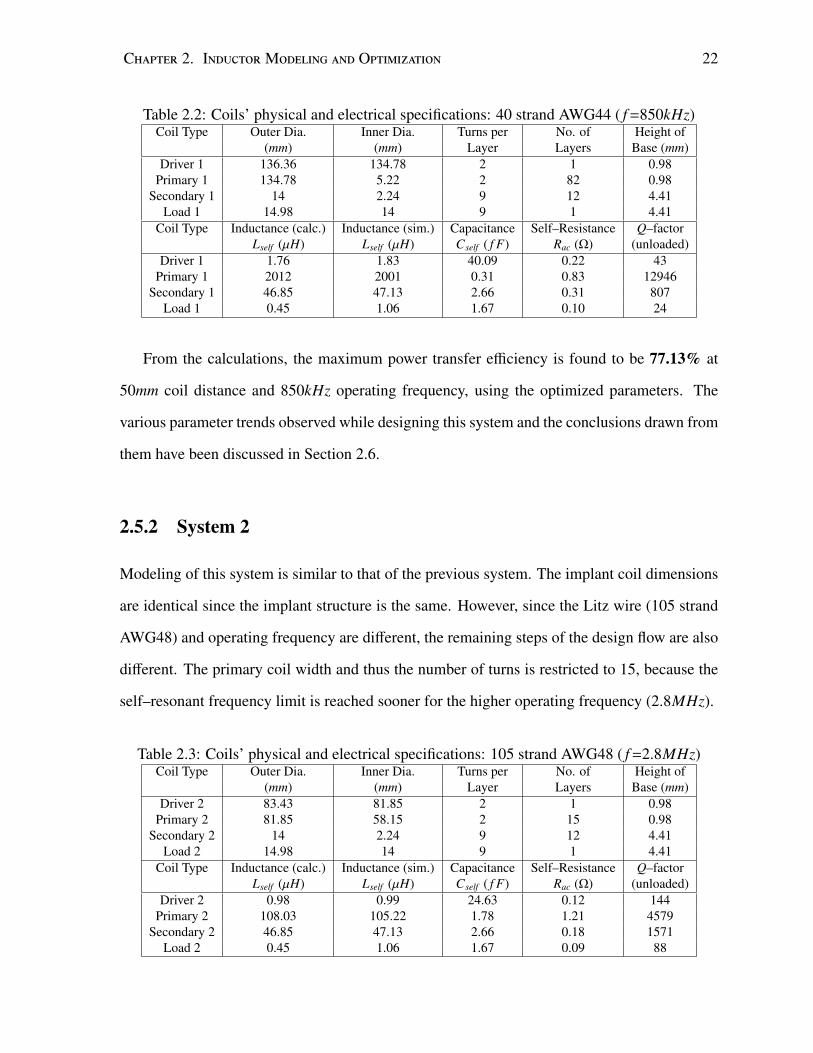
Fig. 2.9 and Fig. 2.10 show this phenomenon of relative immunity to operating frequency
from 400kHz to 1200kHz. However, the output power (PDL) in Fig. 2.9 decreases with in-
creasing frequency because maximum power can only be delivered to the load when half of
the power is dissipated at the source, meaning the efficiency is 50%. This happens at around
300kHz in the graph. In Fig. 2.10, the variation of the power transfer efficiency with the coil
distance is also observed, with peak efficiency being at 50mm, as anticipated.
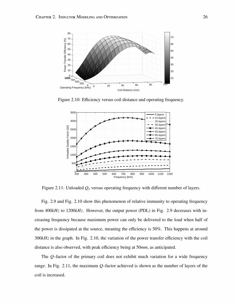
The Q–factor of the primary coil does not exhibit much variation for a wide frequency
range. In Fig. 2.11, the maximum Q–factor achieved is shown as the number of layers of the
coil is increased.

Chapter 2. InductorModeling and Optimization 27
0 2 4 6 8 10 12 14 16 18 202000
4000
6000
8000
10000
12000
Number of Turns
Qua
lity
Fac
tor
(Q2)
0 2 4 6 8 10 12 14 16 18 200
2000
4000
6000
8000
10000
Sel
f−R
eson
ant F
requ
ency
(kH
z)
SRF2Q2
Figure 2.12: Q2 and S RF2 versus number of turns per layer.
2.6.3 Choice of Primary Coil Parameters
As mentioned earlier, the primary coil size is the determined by the typical distance where
efficiency needs to be maximum, which is why we have chosen a radius of 35mm for a coil
distance of 50mm based on (2.17).
For the optimization process to be successful, in System 1, we have used 82 layers for the
primary coil with which the self–resonant frequency SRF is still reasonable (6.4MHz, which is
almost 8 times greater than the operating frequency of 850kHz). Going above 82 layers would
physically require the coil to have a larger radius, which would in turn change the fine–tuning
of the peak efficiency to 50mm. For the primary coil in System 1, the width of the plastic base
is kept at a minimum of 5.22mm, for the spool to be architecturally sound.
For System 2, we have kept the primary coil radius the same because of similar design con-
straints. However, the number of layers Na is decreased to 15, because of the SRF constraint.
For this system, we have a primary coil SRF of 11.5MHz, which is more than 4 times larger
than the operating frequency of 2.8MHz.
For the choice of the number of turns Nt, the determining factor is the output power (PDL)
instead of the efficiency (PTE), which will be discussed in the following chapter that discusses
the overall power transfer circuit. Fig. 2.12 demonstrates how the Q–factor and the SRF of the
primary coil vary with Nt. As can be observed, the Q–factor does not vary much once Nt is

Chapter 2. InductorModeling and Optimization 28
24
68
10
1020
3040
500
2000
4000
6000
8000
10000
12000
Number of TurnsNumber of Layers
Coi
l 2 S
elf−
Res
onan
t Fre
quen
cy (
kHz)
2000
4000
6000
8000
10000
12000
14000
Figure 2.13: Coil 2 SRF versus number of turns and number of layers.
more than 6, which is also true for the SRF. However, both have a steep curve up to 6 turns.
The 3D plot in Fig. 2.13 shows the combined effect of change in Nt and Na on S RF2. It can be
observed that an increase in Na does not drastically reduce the SRF, but rather causes it to have
a gradual response.
2.6.4 Two–Coil versus Four–Coil Systems
The aim of the resonance–based four–coil system is to avoid the problems observed in the two–
coil system, mainly the drastic monotonic decrease of the the power transfer efficiency with an
increase in coil distance due to the low coupling coefficient between the primary and secondary
coils. Fig. 2.14 clearly demonstrates this. It also shows the pre–determined efficiency peak
and the relative immunity of the four–coil PTE for a wide range of coil distances.
2.7 Concluding Remarks
This chapter has throughly discussed all the parameters required for successfully modeling a
multilayer helical inductor coil for RF power transmission. It has developed a optimization

Chapter 2. InductorModeling and Optimization 29
0 10 20 30 40 50 60 70 80 90 1000
10
20
30
40
50
60
70
80
90
Distance (mm)
Pow
er T
rans
fer
Effi
cien
cy (
%)
2−coil4−coil
Figure 2.14: PTE versus distance for 2–coil and four–coil systems.
process for maximizing the power transfer efficiency (PTE) in a four–coil system, and demon-
strated the various design constraints, choices and trends observed during the design flow.
The two systems discussed have been fully developed with the help of the proposed design
and optimization procedure, and their parameters have been tabulated. High efficiency values,
77.13% and 80.66%, have been achieved for both the systems. Graphical plots have been
demonstrated in order to clarify how the various parameters are interlinked, and behave under
different conditions. The stability of the four–coil system in contrast to its two–coil counterpart
has also been established in this chapter.

Chapter 3
Power Transfer Circuit
Although coupled–mode theory has been originally used to to describe resonance–based cou-
pling, it can also be transformed into a simple circuit–based model. This chapter explains the
physics behind resonance–based power transfer and discusses various details of the system
design, such as electrical parameter choices, power harvesting, and application systems. The
power transfer circuit is designed using discrete components that are chosen in accordance to
the specifications of the modeled inductors in the previous chapter.
3.1 Resonance–Based Power Transfer
In 2008, the authors in [40] have investigated and established a non–radiative scheme that
can lead to strong coupling between two medium–range distant long–lived oscillatory resonant
electromagnetic states with localized slowly–evanescent field patterns, that are practical for
efficient medium–range wireless energy transfer.
Although this was the first significant attempt at the resonance–based approach after Nikola
Tesla’s back in 1914, there have been other ways of wireless energy transfer for several pur-
poses till date. These include the following:
• Radiative modes of omni–directional antennas that work well for information transfer but
30

Chapter 3. Power Transfer Circuit 31
are not suitable for energy transfer because of high wastage of energy into free space.
• Directed radiation modes, using lasers or highly–directional antennas, that can be effi-
ciently used for energy transfer even for long distances (distances several times larger
than the characteristic size of the transmitting device), but require existence of an unin-
terruptible line-of-sight and a complicated tracking system in the case of mobile objects.
• Other non–radiative modes such as magnetic induction, but they are restricted to very
close–range or very low–power energy transfers.
The resonance–based method is based on the fact that two same–frequency resonant objects
tend to couple, while interacting weakly with other off–resonant environmental objects, and
even more strongly where the coupling mechanism is mediated through the overlap of the non–
radiative near–field of the two objects [40]. This resonant energy–exchange can be modeled by
the appropriate analytical framework called coupled–mode theory (CMT) [15], and also by the
reflected load theory (RLT) [41].
3.1.1 Coupled–Mode Theory
In this system, the field of the system of two resonant objects 1 and 2 is approximated by
F(r, t) ≈ a1(t)F1(r) + a2(t)F2(r) (3.1)
where F1,2(r) are the eigenmodes of 1 and 2 alone, and then the field amplitudes a1(t) and a2(t)
can be shown to satisfy, to lowest order [15]:
da1
dt= −i(ω1 − iΓ1)a1 + iκa2,
da2
dt= −i(ω2 − iΓ2)a2 + iκa1 (3.2)
where ω1,2 are the individual eigenfrequencies, Γ1,2 are the widths due to the objects’ intrinsic
(absorption, radiation etc.) losses, and κ is the coupling coefficient. Equations (3.2) show that
at exact resonance (ω1 = ω2 and Γ1 = Γ2), the normal modes of the combined system are split

Chapter 3. Power Transfer Circuit 32
by 2κ; the energy exchange between the two objects takes place in time π/2κ and is nearly
perfect, apart for losses, which are minimal when the coupling rate is much faster than all loss
rates (κ >> Γ1,2). The desired optimal regime κ/√
Γ1Γ2 >> 1 is called the “strong–coupling”
regime, which is set as the figure–of–merit ratio for any wireless energy–transfer system, along
with the distance over which this ratio can be achieved.
3.1.2 Reflected Load Theory
The authors in [41] have claimed that although CMT is a more physics–based approach and
RLT is circuit–based, both the methods produce the same results for ICPT. However, CMT
produces relatively simplified equations but works only for very low coupling and high-Q coils.
In the RLT method, the resistive load Rload is transformed into a reflected load onto the primary
loop at resonant frequency. It has been shown that the highest PTE across such inductive links
can be achieved when all LC–tanks are tuned at the same resonance frequency [29].
3.2 Circuit Specifications
The model for the resonance–based four–coil power transfer system consists of lumped equiva-
lent circuits for the four inductors, referred to as driver, primary, secondary and load coils (also
denoted as coils 1 to 4), as shown in Fig. 3.1. In the four–coil system, the high–Q primary
and the secondary coils compensate for the low–Q of the source and load coils and the low
coupling of the intermediate coils.
The coils are tuned to the operating frequency by varying the tuning capacitance Cn for
the given self–inductance as per the equation ω = 1/√
LnCn . For our example case, a voltage
source E of 10.2V is used. A source resistance Rsource of 50Ω and a resistor Rsense at 5.5Ω to
mimic the source resistance of a power amplifier are used in the first loop, as shown in Fig.
3.2. Lastly, a typical load resistance for implant circuitry Rload at 100Ω is included in the last
loop of the circuit, apart from the lumped equivalent components of the inductor coils.

Chapter 3. Power Transfer Circuit 33
Cself
RacLself
Figure 3.1: Lumped equivalent circuit of the inductor.
L1 L2 L3 L4
R1 R2 R3 R4
Rsense
Rsrc
C1 C2 C3 C4k23
E
Rload
Figure 3.2: Electrical model for the power transfer system.
When circuit theory in the form of Kirchoff’s Voltage Law (KVL) is applied to the system,
we achieve the following matrix that defines the relationship between voltage applied to the
driver coil and current through each coil [17]:
I1
I2
I3
I4
=
Z11 Z12 Z13 Z14
Z21 Z22 Z23 Z24
Z31 Z32 Z33 Z34
Z41 Z42 Z43 Z44
−1
E
0
0
0
(3.3)
whereZmn = Rn + jωLn + 1/ jωCn, for m = n
= jωMmn, for m , n
Coupling coefficients k13, k24 and k14 are neglected due to the small size of the driver and
load coils and relatively large distances between the respective coils. Therefore, the matrix
elements Z13, Z14 and Z24 are taken as zero so that they do not have an effect on the results.

Chapter 3. Power Transfer Circuit 34
3.3 Input and Output Power
The ratio of the output power over the input power determines the power transfer efficiency.
It is an extremely important parameter in wirelessly–powered biological implants because of
safety issues and standards regarding tissue exposure to RF electromagnetic radiation [42].
Therefore, maximizing the efficiency will guarantee a relatively high power output at the load
even with a relatively low power wave that has to travel through the body.
However, the optimization of the efficiency does not automatically optimize the output
power. In cases where we are safely below the exposure limit, and we require a high power
delivered to the load (PDL), we can choose to maximize it, even if it at the cost of a lower
power transfer efficiency (PTE).
The matrix in (3.3) can be solved for various circuit parameters. For our purposes, we can
solve it for the input power and the output power at load resistance Rload, which produces the
following equations:
Psource = EI1, Pload = I42Rload (3.4)
where E and Rload are taken from the circuit’s example case as 10.2V and 100Ω respectively.
Replacing I4, we can achieve the following version of the equation:
Pload = Rload
jω3M12M23M34L2L3√
L1L4 E√
L1L2√
L2L3√
L3L4 (M212M2
34ω4 + Z11Z22Z33Z44 + ω2(M2
12Z33Z44 + M223Z11Z44 + M2
34Z11Z22))
2
(3.5)
The equation (3.5) determines a direct relationship between the actual power delivered
to the load (PDL) and characteristics of the designed inductor such as its self and mutual
inductance, stray capacitance and AC resistance. Therefore, we can use this equation in our
proposed optimization process directly to maximize the PDL, in a similar approach that was
taken to maximize the power transfer efficiency (PTE) in the previous chapter. This is how a
PDL versus PTE trade–off can be achieved depending on application requirements.

Chapter 3. Power Transfer Circuit 35
0
50
100 05
1015
200
50
100
150
200
Number of TurnsDistance (mm)
Pow
er D
eliv
ered
to L
oad
(mW
)
20
40
60
80
100
120
140
160
180
(a)
0 20 40 60 80 1000
50
100
150
200
Coil Distance (mm)
Pow
er D
eliv
ered
to L
oad
(mW
)
1 turn2 turns3 turns4 turns5 turns6 turns7 turns8 turns
(b)
Figure 3.3: (a) 3D plot for PDL versus coil distance and number of turns. (b) 2D plot for PDLversus coil distance for up to 8 number of turns.
3.3.1 Effect of Number of Turns on Peak Power
In contrast to the radius of the external inductor being used to tune the efficiency to a certain
coil distance, the PDL tuning is dependent on the height (number of turns) of the external
inductor. To demonstrate this, we have conducted a sweep for PDL versus number of turns for
a range of coil distances, showed in Fig. 3.3(a) and 3.3(b).
In these graphs, it is observed that the general trend is that the peak PDL will be at a
smaller distance as the number of turns increase. The recession of the peak is very distinct

Chapter 3. Power Transfer Circuit 36
0 20 40 60 80 1000
15
30
45
60
75
90
Coil Distance (mm)
Pow
er T
rans
fer
Effi
cien
cy (
%)
1 turn2 turns3 turns4 turns5 turns10 turns15 turns20 turns
Figure 3.4: PTE versus coil distance for several number of turns.
with increasing number of turns and for our typical coil distance of 50mm, we would require
about 2 turns only to maximize PDL, which has been incorporated in our two system designs.
From Fig. 3.4, it can be observed that the efficiency peak does not vary significantly with
increasing number of turns and for a higher number of turns, the efficiency is quite uniform
across the range of distances.
3.3.2 Effect of Source Resistance
As shown in Fig. 3.5, the source resistance does not have a significant effect on the power
transfer efficiency. PTE peaks slightly higher and at a slightly smaller distance with a lower Rs.
0 20 40 60 80 1000
10
20
30
40
50
60
70
80
90
Distance (mm)
Pow
er T
rans
fer
Effi
cien
cy (
%)
Rs=25OhmRs=50OhmRs=75OhmRs=100OhmRs=125OhmRs=150Ohm
Figure 3.5: PTE versus coil distance for different source resistances.

Chapter 3. Power Transfer Circuit 37
0 20 40 60 80 10010
15
20
25
30
Distance (mm)P
ower
(dB
m)
0 20 40 60 80 1000
20
40
60
80
Effi
cien
cy (
%)
EfficiencyI/P PowerO/P Power
Figure 3.6: Input power, output power, and efficiency of System 1.
0 20 40 60 80 100−10
−5
0
5
10
Distance (mm)
Pow
er (
dBm
)
0 20 40 60 80 1000
20
40
60
80
Effi
cien
cy (
%)
EfficiencyI/P PowerO/P Power
Figure 3.7: Input power, output power, and efficiency of System 2.
3.3.3 Results
After performing the optimization of the output power, we have achieved high values for sys-
tems 1 and 2 described in Chapter 2, that is shown in Fig. 3.6 and 3.7.
For the coils in System 1, a PDL of 22.3dBm has been achieved for 50mm coil distance.
For the high frequency coils in System 2, a PDL of 0.76dBm has been achieved for the same
distance. Therefore, our systems have been optimized in a way so that both PTE and PDL are
maximized at the same distance between primary and secondary coils.
It is to be noted that for the System 2 circuit, we have chosen an Rload value of 1kOhm and
a voltage source of only 1V , since it was the requirement for our power harvesting circuit in
[43]. Also, for both the systems, the optimized operating frequency was the lower limit of the
respective Litz wire, 350kHz and 1.4MHz respectively. Therefore, it can be concluded that
the lower operating frequency limit produces higher PDL values whereas the higher operating
frequency limit produces higher PTE values.

Chapter 3. Power Transfer Circuit 38
8.08V
850kHz
C1=10uF
C2=10uF
Rload=100Ω
R1=val
R2=1kΩ
Vin Output
Shdn' Adj
Figure 3.8: Power harvesting unit with rectifier and voltage regulator blocks.
3.4 Power Requirements and Harvesting Unit
So far we have only considered the transmission of power from the external circuitry to the
implant coil. But the power in this form is not suitable for direct consumption by the implant.
Therefore, we have designed a power harvesting circuit that rectifies and regulates the output
power into a constant DC form.
Since the power requirements will vary as per the application of the implant, the power
harvester circuit has been designed assuming a load resistance of 100Ω for the architecture of
System 1 in Chapter 2. This system has a voltage output of 8.08V at 850kHz, which is taken
as the input voltage to the power harvesting circuit in Fig. 3.8.
The power harvester is entirely made up of discrete components. The system of diodes
is a full–bridge rectifier or AC–to–DC converter. We have used the commonly–used D1N914
diode, which has a high switching speed and low forward voltage drop (≈ 0.6V). Any diode
with similar rating can be used for the rectifier section. The capacitor C1 is for smoothing the
output waveform, and has been calculated using the following relations:
Vdc = Vac − 2VD; r ≈Vdc
2 fC1Rload(3.6)
where Vac is the AC input, Vdc is the DC output, VD is the forward voltage of the diode and r is
the height of the ripple in the output waveform.

Chapter 3. Power Transfer Circuit 39
0 0.1 0.2 0.3 0.4 0.5 0.6 0.7 0.8 0.9 10
100
200
300
400420
500
Time (ms)
Out
put P
ower
(m
W)
Rval
=100 Ohm
Rval
=250 Ohm
Rval
=400 Ohm
Rval
=550 Ohm
Rval
=700 Ohm
Rval
=750 Ohm
Figure 3.9: Output power versus time for different values of Rval.
Next we have a voltage regulator or DC–to–DC converter for forcing the output voltage to
a certain constant value. For this purpose we have used the LT1121 micropower low dropout
regulator with shutdown from Linear Technology. It has a dropout voltage of 0.4V and a 150mA
output current.
Its four pins can be configured as per the requirements. The Shutdown pin has been shorted
with the Vin since we are not using that feature. The Output and and the Adjust pin have been
arranged as a potential divider so that the output voltage at Rload can be adjusted by changing
the value of R1, thereby changing the R1/R2 ratio. Without the potential divider, the output
voltage would be a constant of 3.75V for this regulator.
The graph in Fig. 3.9 shows how the output power varies for different values of R1, and
saturates somewhere above R1 = 700Ω. The maximum power output that can be achieved
with this circuit for an R1 of 750Ω or higher is 420mW, which is suitable for typical biological
implant applications.
3.4.1 Charge Pump
The charge pump is an optional section to the power harvester unit, which can be added in order
to amplify the input voltage to the harvester. For demonstrating the voltage amplification, we
have created a charge pump out of discrete components, shown in Fig. 3.10.

Chapter 3. Power Transfer Circuit 40
C1=10uF
C2=10uF
C3=10uF
C4=10uF
8.08V
850kHz
R=100Ω
Figure 3.10: The charge pump unit.
0 50 100 150 200 250 300 350 400 450 5000
5
10
15
20
25
30
Time (us)
Out
put V
olta
ge (
V)
Vin
=2.08V
Vin
=4.08V
Vin
=6.08V
Vin
=8.08V
Figure 3.11: Output voltage versus time for different values of Vin.
This charge pump is a typical variation of the Dickson’s charge pump [44]. The input
voltage signal is offset by the shunt diode, and the resulting signal is then rectified by the series
diode. By stacking a number of charge pump stages, the voltage signal can be multiplied to a
much higher value, although adding too many stages also increases the parasitic capacitance of
the diodes and the output impedance of the multiplier.
The designed charge pump uses the same voltage input from System 1, and capacitors with
a low value of 10uF in order to speed up the transient response. It can replace the rectifier unit
of the power harvester, if a higher power output is required for the implant application circuitry.
Fig. 3.11 shows that for the input voltage of 8.08V , a voltage of 26V is achieved at the output
of the charge pump.

Chapter 3. Power Transfer Circuit 41
Power
Source
End Device
PC/Embedded
External
Unit
Internal
Unit
Power
Harvesting
Unit
Microcontroller
RF
Transceiver
Interface
Electronics
Application
Wireless Power
Transfer
Wireless Data
Transfer
700 kHz
2.4 GHz
Figure 3.12: Block diagram of overall system: external and internal sub–blocks.
3.5 Typical Application Systems
Wireless power delivery can be used for numerous applications of modern autonomous elec-
tronic devices such as cell phones, laptops and household robots. For our project, we are using
it for implantable bio–sensors. This section presents a generic version of such a system, in
order to demonstrate the functions of its various components [38].
The implantable system incorporates the receiver coils designed in the previous chapters.
The overall system is divided into two units: external and internal (Fig. 3.12). The external unit
includes both a power delivery section and an end device. The power delivery section contains
a larger transmitting coil, which is connected to a wired power source, and is designed to allow
for maximum power transfer to the smaller implant coil. The second sub–block is the end
device, which can refer to a computer or a more application–specific embedded system. The
end device is connected wirelessly to the internal unit through a wireless data–link (antenna).
The implantable internal unit is a small application–specific system, designed to capture

Chapter 3. Power Transfer Circuit 42
bio–sensor data using a custom interface board and communicate it to the end device for further
processing. The implantable unit contains three main sub–blocks, a power–harvesting block, a
processing and transceiver block, and an application–specific interface block.
The power harvesting section of the internal system comprises of the inductor coil con-
nected to other components to regulate and increase the reliability of the input power to the
implant. Apart from the discrete component level power harvesting unit designed in Section
3.4, an Integrated Circuit (IC) level design of the power harvester has also been simulated
in CMOS 0.13µm technology [43]. The design consists of a low–voltage low–power voltage
regulator, which includes a charge pump and a temperature insensitive voltage reference.
The internal unit contains a microcontroller and an RF transceiver, that preferably have
a low power consumption. The data is transmitted to the end device using Frequency Shift
Keying (FSK) modulation at a frequency of 2.45 GHz. This allows the system to work in the
Industrial, Scientific and Medical (ISM) band, which allows existing antenna technologies and
devices to be used, while reducing developmental time and cost. Any signal processing and
data compression is done in the microcontroller before it is sent to the end device.
The interface block of the implant includes bio–sensors that can be used for various ap-
plications such as temperature and blood pressure monitoring. The interface electronics are
custom to the application in order to reduce the power consumption of the system. Overlap-
ping application areas may use the same or similar electronics, further reducing the size and
power consumption of the system. The implantable system is able to be modified to be im-
planted into lab subjects of various sizes and for different applications. Only modifications to
the interface electronics and inductor design are required.
3.6 Summary
This chapter implements the inductors designed in this research in the actual implant circuit.
It gives a clear overview of the theory behind resonance–based power transfer and how the

Chapter 3. Power Transfer Circuit 43
coupled–mode theory can be translated into a more circuit–based approach. The circuit speci-
fications thoroughly define all the components of the power transfer block of the external and
implant circuits, including the lumped equivalents of the four inductors. Circuit theory calcula-
tions are used to derive direct relationships between output power and the inductor parameters,
so that optimization of output power can be performed by reusing the procedure developed for
efficiency optimization.
A novel relationship has been observed between the number of turns of the coil and position
of the peak output power in Section 3.3.1. It shows that a greater number of turns shift the peak
power to a smaller coil distance. This knowledge will enable future inductor designers to
fine–tune their coils as per very specific application requirements. Also, the effect of source
resistance on efficiency has been noted.
The results of the optimization procedure have been graphically demonstrated for the two
systems described. System 1 has a PDL of 22.3dBm and System 2 has a PDL of 0.76dBm
for their respective specifications. Conclusions have been drawn on the optimal frequency for
maximum output power.
In this chapter, a power harvesting unit and a charge pump have been designed to rectify,
regulate and amplify the output voltage of the power transfer circuit. A power output of 420mW
has been achieved with the power harvester and a voltage output of 26V has been achieved with
the charge pump. Lastly, a typical implant application system has been described with all of its
sub–components.

Chapter 4
Misalignment Analysis
Most of the studies conducted so far on wirelessly–powered biological implants deal with
standard scenarios where the subject would be at a constant distance and/or position from the
external circuitry. Some studies, such as [1] and [45] have addressed the issue of misalignment,
but have not delved into it as far as the effects and boundaries of misalignment are concerned.
Therefore, in this thesis, we have conducted analysis and calculations on axial and angular
misalignment of the primary and secondary coils, with conclusions on the feasibility of the
power transfer circuit and allowable worst–case alignments of the two inductors.
4.1 Mutual Inductance with Misalignment
4.1.1 Overview
An inductive link can be compared to a loosely–coupled transformer for various electromag-
netic applications, where the magnetic field generated by the primary coil is partially picked
up by the secondary coil, thus enabling wireless power transfer. However, this system needs
to be optimized for misalignment tolerance when the implant is meant for living biological
subjects. Any misalignment directly affects the mutual inductance, which in turn reduces the
overall power transfer efficiency.
44

Chapter 4. Misalignment Analysis 45
Therefore, the formula to find mutual inductance for circular coils in air has to take into
consideration both axial and angular misalignments. This research area has a long history of
contributions in electrical engineering. A lot of research has been based on the application
of Maxwell’s formula, Neumann’s formula and the Biot–Savart law; as well as the use of
analytical or semi-analytical forms expressed over elliptic integrals of the first, second and third
kind, Heuman’s Lambda function, Bessel functions, and Legendre functions. The problem can
also be addressed by using numerical methods, such as the finite element method (FEM) and
the boundary element method (BEM).
In this research, we have adopted the approach taken by [46] and [20] that uses the filament
method, where coils of rectangular cross–section are replaced by a set of filamentary circular
coils. The formulas stated here yield Maxwell’s well–known formula for mutual inductance of
two circular coils, when the coils are parallel and coaxial. The mutual inductance is calculated
using series that converge slowly, and is a good alternative to numerical methods.
4.1.2 Cases of Misalignment
The expression for mutual inductance has already been given in Chapter 2 in the form of
equations (2.1) and (2.2). They are restated below for the convenience of the reader:
M =µ0
π
√RPRS
π∫0
(cos θ − dRS
cos φ)Ψ(k)√
V3dφ (2.1)
M =
N1N2
g=K∑g=−K
h=N∑h=−N
l=n∑l=−n
p=m∑p=−m
M(g, h, l, p)
(2S + 1)(2N + 1)(2m + 1)(2n + 1)(2.2)
These equations deal with both the axial and angular misalignment cases. However, there are
more details about the orientation of the inductors that need to be taken care of while using
these equations. This will be the topic of discussion for this subsection, where we will prove
the universal nature of (2.1) and (2.2).

Chapter 4. Misalignment Analysis 46
The well–known filament method [22] along with equations (2.1) and (2.2) are used for
the calculation of the mutual inductance between all pairs of inclined circular coils either with
rectangular cross or negligible section. In the calculations, we have to take into account two
coils where the axis of the primary coil will be the axis z and the axis of the secondary inclined
coil will be the axis z′ . In this treatment, it is important to distinguish two cases given below,
for which the choice of calculation methods would be different [20]:
• Centers of the filamentary circular coils which replace the secondary inclined coil lie in
different points away from the axis of the primary coil.
• All centers of the filamentary circular coils which replace the secondary inclined coil lie
in the same point of the axis of the primary coil or they lie in the same point of the axis
of the secondary coil.
A detailed analysis of the cases can be found in [20]. For the case where the center of the
secondary coil lies in the same axis as that of the primary coil, instead of applying the filament
method to (2.1), it is applied to the following equation:
M =µ0
π
√RPRS cos θ
π∫0
Ψ(k)√
V3dφ (4.1)
whereV =
√1 − cos2 φ sin2 θ ,
k2 =4αV
(1 + αV)2 + ξ2 , ξ = β − α cos φ sin θ,
Ψ(k) =
(2k− k
)K(k) −
2k
E(k), α =RS
RP, β =
cRP.
It can be observed that (4.1) is a simpler form of (2.1), and can be easily achieved by
making the axial distance d = 0. This implies that the centers of both the coils lie on the same
axis. Therefore, for our design, using (2.1) and (2.2) based on only the first case will suffice.
The second case is almost irrelevant for our purpose since it is now only used when the
secondary coil is a thin disk coil, as shown in Fig 4.1. However, if we do choose to go with a

Chapter 4. Misalignment Analysis 47
a
hP
hS
RP
RS
c
d
θ
x,y
x',y'z
z'
2n+1
2K+1
2N+1
N1 turns
N2 turns
Figure 4.1: Cross–section of two non–coaxial and non–parallel circular coils, where the sec-ondary coil is a thin disk coil, represented by a single filamentary coil.
single–turn secondary coil, we can again use the same set of equations (2.1) and (2.2) for the
second case, by suppressing the variable deciding the number of turns (p = m = 1) in (2.2) and
making d = 0 if the coils are coaxial.
Another equation that has been stated in [47] deals with only the non–coaxial case, with
the axes of the two coils being parallel:
M =µ0
π
√RPRS
π∫0
(1 − dRS
cos φ)Ψ(k)√
V3dφ (4.2)
where
V =
√1 +
d2
R2S
− 2d
RScos φ ,
k2 =4αV
(1 + αV)2 + β2 , α =RS
RP, β =
cRP,
Ψ(k) =
(2k− k
)K(k) −
2k
E(k).
This case too, as shown in Fig. 4.2, can be ignored for our purpose because (2.1) collapses
into this form when θ = 0, thus making the term cos θ = 1.

Chapter 4. Misalignment Analysis 48
a
hP
hS
b
RP
RS
c d
x,y
x',y'
z z'
2m+1
2n+1
2K+1
2N+1
N1 turns
N2 turns
Figure 4.2: Cross–section of two non–coaxial but parallel circular coils.
Therefore, the conclusion on the use of different formulas of mutual inductance for differ-
ent misalignment cases is that using the general case stated in Chapter 2 is the most efficient
method. Other cases can be achieved by assigning appropriate values to the variables involved.
4.2 Techniques for Calculation
Essentially, any numerical solver can be used to apply the formulas and produce results. We
have used the software MATLAB R© for the calculation purposes. A function–based modular
approach proved to be the most efficient method for performing the mutual inductance calcu-
lations. The flowchart in Fig. 4.3 demonstrates the sequence of these functions starting from
the optimization level down to the integration level.
We have chosen the Romberg’s Method function (rombint) that is predefined in the software
to perform the integration given in the expression (2.1). This method is used to estimate definite
integrals. The variable f un f cn describes the integrand of the variable φ and is called from a
separate module, which consists of all the intermediate values such as V , k2 and Ψ(k). The
domain of integration is from a to b, which are set to 0 and π in our case.

Chapter 4. Misalignment Analysis 49
Functions for
other parameters
rombint (funfcn, a, b)
for Romberg Integration
funfcn: Integrand containing
all intermediate values
Function handle for
mutual/self inductance
Function performing PTE/PDL optimization
Figure 4.3: Sequence of function calls to perform mutual inductance calculations.
The main code performing the inductance calculations (stored in a file called ‘inductance.m’)
simply calls the rombint function (stored in a file called ‘rombint.m’), declaring its parameters
as the integrand f un f cn (stored in a file called ‘integrand.m’ in our case), the lower bound 0
and the upper bound π. A detailed sequential structure of the MATLAB program is tabulated
in Tables 4.1 and 4.2.
4.3 Results and Discussion
As stated in the beginning, this chapter is meant to establish strict boundaries on the extent of
misalignment between the primary and secondary coils. It needs to be noted that misalignment
cases are not considered between the source and primary coils, and the secondary and load
coils, since they are wound co–centrically over the same central structure (a plastic base).
The graphs in Fig. 3.6 and 3.7 in the previous chapter have demonstrated input power,
output power and efficiency values for different coil distances, calculated with the help of
numerical analysis. However, the coils there were considered to be aligned parallelly, with
their centers along the same axis.
By using the equations (2.1) and (2.2), and then (2.3), which states the relationship between
self and mutual inductance of a coil pair, we are able find the coupling coefficient k23 for
all types of misalignment cases, which could otherwise only be found empirically through
measurements. Once we have the value of k23, we can replace it in the power.m function in
order to find the input and output power of the power transfer circuit.

Chapter 4. Misalignment Analysis 50
Table 4.1: Detailed sequence of MATLAB functions used in the optimization process (Part 1)
MAIN CODE: optimization.m
• Declaration of all physical properties as global variables such as radius, height, width,distance, number of turns and layers, frequency etc.
• Opening of a text file to save parameter values.
• Code to perform optimization process as per flowchart in Fig. 2.6.
• Calling separate functions for each parameter calculation (described below):
1. inductance.m 2. resistance.m 3. self res freq.m 4. q fac eff.m 5. power.m
1. inductance.m
• Separate codes for all self–inductances (L1, L2, L3, L4) and mutual inductances (M12,M34, M23). M13, M24, M14 neglected (later set to 0) due to size and distance of inductors.
• Calculation of k12, k34, k23 from Lm, Ln and Mmn values.
• Each inductance calculation involves the following:
– Assigning values to variables a, b, c, d, RP, RS , hP, hS , N1, N2 from the values declaredin optimization.m for the global variables.
– Variables N, K, n, m set to 6 (can be set to a higher or lower value to increase ordecrease accuracy of calculation as well as speed of code execution.
– Nested for loops run for variables h, l, g, p, inside which calculations are performedfor z(g, p), RP(h), β(h, g, p), RS (l), α(h, l) and M(h, l, g, p).
– For calculating M(h, l, g, p), the rombint.m and integrand.m functions are called withthe command out = rombint(@integrand, 0, π).
1.a) integrand.m 1.b) rombint.m
• Declaration of function M(h, l, g, p) =
integrand(φ).
• Declaration of global variables RP(h),β(h, g, p), RS (l), α(h, l).
• Performing calculations for V(l), k2,K(k), E(k), Ψ(k) and M(h, l, g, p).
• Predefined function built intoMATLAB.
• No changes required.

Chapter 4. Misalignment Analysis 51
Table 4.2: Detailed sequence of MATLAB functions used in the optimization process (Part 2)
2. resistance.m
• Assigning values to variables and performing resistance (both DC and AC) calculations.
• Equations (2.8) and (2.9) were used for System 1 and equations (2.10) and (2.11) wereused for System 2.
• If finding value of η to find fh in (2.10), values are interpolated from the graph given inFig. 2.3 by using the built–in MATLAB function spline.
3. self res freq.m
• Assigning values to variables and performing calculations for stray capacitance Csel f asper equations (2.4), (2.5) and (2.6).
• Finding the self–resonant frequency fsel f from self–inductance Lsel f (from inductance.mfunction) and Csel f values by using (2.7).
• Using fsel f to find Le f f and ES R values, which are the effective inductance and effectiveseries resistance respectively.
4. q fac eff.m
• Finding values of Q1, Q2, Q3, Q4 from Le f f and ES R values calculated inself res freq.m. For Q1 and Q4, source and load resistance values are added to ESRin order to make it loaded Q–factor.
• Calculating efficiency from coupling coefficients kmn (from inductance.m function) andQ–factor values by using formula in (2.16).
5. power.m
• Assigning values to voltage source E, kmn, and Rn, Ln, Cn for each inductor coil n.
• Nested for loops run for m and n to define the KVL matrix in (3.3), in order to find thecurrent through each loop In.
• Finding values of Pin, Pout and Vout by using simple electrical relations.

Chapter 4. Misalignment Analysis 52
0 5 10 15 20 25 300
0.02
0.04
0.06
0.08
0.1
0.12
0.14
0.16
0.18
0.2
Axial Distance d (mm)
Cou
plin
g C
oeffi
cien
t k23
c=10mmc=20mmc=30mmc=40mmc=50mm
(a)
0 20 40 60 80 1000
0.02
0.04
0.06
0.08
0.1
0.12
0.14
0.16
Angular Separation θ (degrees)
Cou
plin
g C
oeffi
cien
t k23
c=10mmc=20mmc=30mmc=45mmc=50mm
(b)
Figure 4.4: (a) Coupling coefficient k23 versus angular separation θ for different coil distancesc (axial misalignment d is 0). (b) Coupling coefficient k23 versus axial distance d for differentcoil distances c (angular misalignment θ is 0).
Therefore, if a minimum output power value can be identified for a system, which must be
achievable for the implant to operate properly, it is a straightforward process to find the mini-
mum k23 value required. This is how the worst–case values of misalignment can be calculated.
4.3.1 Observations and Modeling
For System 1 and System 2, it is observed in the graphs in Fig. 3.6 and 3.7 that the output
power maintains a minimum value that is about half of the input power (efficiency = 50%) up
to a distance of 75mm, after which it deteriorates. The maximum efficiency for both systems
is at around 50mm, since it is the distance for which the specific external coils (70mm average
diameter) have been designed. At 75mm distance and with perfect alignment between coils, the
power delivered to the load Rload is 18.3dBm for System 1 and -5.55dBm for System 2, which
are typical adequate levels for the operational purpose of small–size biomedical implants.
Using equations presented in Section 4.1, we have defined the coupling coefficient k23 for
various coil distances, and axial and angular misalignments, that have produced the graphs in
Fig. 4.4 and 4.5. Fig. 4.4 demonstrates the effect of one type of misalignment (either axial or
angular), keeping the other constant, for different coil distances.

Chapter 4. Misalignment Analysis 53
020
4060
0
5
10
15
0
0.02
0.04
0.06
Axial Distance d (mm)Angular Separation θ
Cou
plin
g C
oeffi
cien
t k23
0.005
0.01
0.015
0.02
0.025
0.03
0.035
0.04
0.045
0.05
0.055
Figure 4.5: Sensitivity analysis of k23 with respect to both axial and angular misalignments(c=50mm).
The trend, as anticipated, is decreasing coupling coefficient with increasing misalignment,
until k23 drops to almost zero. However, the function will never reach zero exactly but keep
approaching it. A sharp peak is seen in Fig. 4.4(a) for c = 10mm at d = 15mm because at this
point the coil distance c is less than the axial misalignment d, which causes the magnetic field
to be oriented in an unusual pattern.
The 3D graph in Fig. 4.5 shows the simultaneous effects of both types of misalignment, for
a fixed distance of 50mm between the primary and secondary inductors. The color–coding of
this graph can be used to find regions where k23 is higher than a specified minimum value.
4.3.2 Worst–Case Alignment
Since System 2 has been designed as per the requirements of our integrated circuit in [43],
we will consider it as our test–case circuit configuration for analyzing misalignments. This
integrated circuit works well in the sub 1mW power region, specifically between (100µW and
500µW). Therefore, a good power value for us to work with would be 250µW.
At a distance of 75mm between the primary and secondary coils, the output power is a little

Chapter 4. Misalignment Analysis 54
Run optimization code for PTE and PDL
Note k23 value for specified output power
Set typical coil distance for setup
Set power requirement of implant
Run sensitivity analysis on k23 value
Find worst-case alignment
Figure 4.6: Flowchart to find worst–case alignment of primary and secondary coils.
over 250µW (279.5µW precisely). Ideally, similar amounts of power should still be achievable
regardless of the inductor orientation. Therefore, an analysis in order to find the worst–case
alignment at which 250µW of power is still deliverable to the 1kOhm load has been conducted
using the specified equations and graphs. The steps involved are outlined in Fig. 4.6.
To begin with, we note the value of the coupling coefficient k23 at the 75mm coil distance.
Calculating k23 from equations (2.1), (2.2) and (2.3), we get a value of 0.032. This implies that
k23 needs to be at least 0.032 for a minimum of 250µW of power delivery to the load. From
the sensitivity analysis graphs given, it is observed that k23 approximates this value when the
primary and secondary coils are apart by
• 75mm but perfectly aligned (from Fig. 3.6 and 3.7);
• 50mm with axial distance of 22.5mm, but parallel (from Fig. 4.4(a));
• 50mm with angular separation of 55, but coaxial (from Fig. 4.4(b));
• 50mm with axial distance of 10mm and angular separation of 37.5, or alternatively, with
axial distance of 5mm and angular separation of 45(from Fig. 4.5).
The above–mentioned orientations are the worst–case alignment cases for System 2 to
operate successfully with an integrated–circuit biological telemetry system implanted inside

Chapter 4. Misalignment Analysis 55
Figure 4.7: Typical subject (mouse) with implanted telemetry system powered by external coil.
a freely–moving subject. Misalignments beyond the orientations considered will reduce the
power delivery too much with respect to the specified requirement and the implant circuit will
potentially fail to operate.
The best method to physically implement this system is to have the larger coil (driver–
primary coil pair) at the bottom of the cage in which the subject is housed, as shown in Fig.
4.7. The walls of the cage should be distanced as such so that the subject is physically unable
to cross the axial misalignment boundaries. The angular misalignment boundary is capacious
enough to allow for tilted or sleeping positions of the subject.
However, when the implant coil is at 90 angular misalignment, the magnetic flux linkage
becomes zero, thus enabling no power transfer. This problem can be avoided with the use
of a Helmholtz configuration [48] (with two external coils, each at the top and bottom of the
cage), or having more than one implant coil in the form of an array. These implementations
will require extensive modifications to be made to the overall system design and are outside
the scope of this research work.

Chapter 4. Misalignment Analysis 56
4.4 Summary
This chapter has dealt with the issue of coil misalignment for the case of freely–moving biolog-
ical subjects. It has given a thorough description of the different types of possible misalignment
cases and what techniques are present for calculating them. It has demonstrated the approach
we have taken for calculating coil misalignments for the two designed inductively–coupled
power transfer systems.
The series of MATLAB R© codes that have been created to implement the overall optimiza-
tion and modeling of the inductive system, taking care of coil misalignment, has also been
given in this chapter. The detailed modular structure of the program will enable future design-
ers to have a better idea regarding implementation procedures.
Sensitivity analysis based on System 2 given in Chapter 2 has been conducted for axial and
angular misalignments, as well as the simultaneous effect of both types. Worst–case alignments
have been specified for a minimum power supply of 250µW to the power harvester in [43]
using System 2 specifications. It has been shown that if a certain coupling coefficient number
is known and needs to be matched, boundaries of misalignment can be calculated for axial,
angular and simultaneous cases, by following the series of steps summarized in Fig. 4.6.

Chapter 5
Finite Element Method Modeling and
Surrounding Environment of Coils
Numerical methods can be implemented in order to verify some of the results we have gathered
so far in the previous chapters. This will offer a more solid proof to the analyses conducted and
pave the way to manufacturing of the proposed designs. Therefore, this chapter includes the
numerical method modeling that has been conducted using the Finite Element Method (FEM)
by using commercial software products called COMSOL R© and EMPro R©. Important electrical
parameters of the coils have been evaluated using these software simulations.
This chapter also deals with current standards on the permissible extent of RF radiation
and exposure, as well as the effects of the inclusion of external materials including biological
matter into the model, since it will be an issue in the real–life operation of the implants.
5.1 Introduction to the Finite Element Method
The finite element method (FEM) is a numerical technique for finding approximate solutions of
partial differential equations (PDE) and their systems. In simple terms, FEM is a method for di-
viding up a very complicated problem into small elements that can be solved in relation to each
other. Although it has its origin in the field of structural analysis, it is now employed in diverse
57

Chapter 5. Finite ElementMethodModeling and Surrounding Environment of Coils 58
areas such as waveguide problems, electric machines, semiconductor devices, microstrips, and
absorption of EM radiation by biological bodies [49].
Although the finite difference method (FDM) and the method of moments (MOM) are con-
ceptually simpler and easier to program than the finite element method (FEM), it is a more
powerful and versatile numerical technique for handling problems involving complex geome-
tries and inhomogeneous media. The systematic generality of the method makes it possible to
construct general-purpose computer programs for solving a wide range of problems. Conse-
quently, programs developed for a particular discipline have been applied successfully to solve
problems in a different field with little or no modification [50].
The finite element analysis of any problem basically involves the following steps:
• Discretizing the solution region into a finite number of subregions/subdomains, called
finite elements;
• Interpolating solution for each element;
• Deriving governing equations for a typical element;
• Assembling of all elements in the solution region;
• Solving the system of equations obtained;
• Post–processing to generate solutions to required parameters.
Discretization of the continuum involves dividing up the solution region into subdomains,
called finite elements. Some typical elements for one–, two–, and three–dimensional problems
can be lines, triangles, rectangles, quadrilaterals, tetrahedrons and hexahedrons constituting
different number of nodes.
All of the above–mentioned steps are nowadays solved automatically with the help of de-
veloped FEM–based software, so the need for hands–on calculations has dramatically reduced.
However, the basic principles will enable the reader to visualize the requirements, techniques
and application of such a vastly popular numerical method.

Chapter 5. Finite ElementMethodModeling and Surrounding Environment of Coils 59
5.2 COMSOL R© 2D Electromagnetic Simulations
This section describes the simulations performed by the software, primarily in order to verify
the results for coil resistance, coil self–inductance, and coil mutual inductance with and without
misalignments. The version of the COMSOL software used was 4.2a, which contains all the
necessary modules for our electromagnetic simulations.
5.2.1 Model Setup
A model in COMSOL needs to be set up by following some predefined criteria. The steps
involved in setting up the model are given below:
• Two–Dimensional Model Setup: The 2D model was set up in the 2D axisymmetric
dimension. This choice of dimension is very helpful in simplifying complicated 3D
geometries and significantly reducing simulation time, since it works with only a cross–
section of the geometry and combines the results to 3D at the end.
The physics added was Magnetic and Electric Fields (mef) under the AC/DC module.
Lastly, the type of study was chosen as Frequency Domain with a frequency of 2.8MHz.
• Geometry, Materials and Mesh: The geometry was defined in millimeters as arrays
of circles for the primary and secondary helical coils. The boundary was chosen as a
semicircle (for sphere in 3D).
The material assigned to the boundary was Air with infinite elements, and to the coil
domain was Copper, with slightly modified parameters due to the use of Litz wire. Lastly,
the mesh chosen was a coarser triangular mesh (Fig. 5.1).
• Governing Equations: The coils were assigned with the predefined Multi-turn Coil
Domain feature of COMSOL. It adds an externally generated current density to the right–
hand side of the equation that the Magnetic Fields interface defines. This feature sets the
conductivity of the domain to zero because the induced current in the coil windings is

Chapter 5. Finite ElementMethodModeling and Surrounding Environment of Coils 60
Primary
Coil Domain
Secondary
Coil Domain
Figure 5.1: 2D coil setup in COMSOL and coarser triangular mesh.
handled in a homogenized manner. The external current density can be calculated in
different ways, depending on whether a total current or a total voltage is specified. This
definition uses the following governing equations:
( jωσ − ω2ε0εr)A + ∇xH − σvxB = Je (5.1)
Je = NIcoil/acoil (for current–driven coil) (5.2)
Rcoil = A∫
NL/σcoilacoilA (5.3)
Lcoil = 2Wm/I2 (5.4)
Mi j = Φi j/I j = ( j/ω)(Vinduced,i j/I j) (5.5)
The terms in the above equations follow basic electromagnetic notations. The primary
coil domain was assigned with an excitation of 1A, while the secondary coil domain was
set to zero. This was done in order to calculate the induced voltage in the secondary coil.

Chapter 5. Finite ElementMethodModeling and Surrounding Environment of Coils 61
Figure 5.2: Magnetic flux density (normal) and electric field (normal).
5.2.2 Simulation Results
The model was simulated with the given setup and specifications, and 2D plots were generated
for the magnetic flux density and the electric field, as shown in Fig. 5.2. From the figure, it is
evident that both the magnetic flux density and the electric potential is maximum around the
primary coil domain, since it has been excited with a current of 1A. However, these parameters
are not zero around the secondary coil, because of the magnetic flux linkage that causes some
amounts of induced voltage in it.
Results for other parameters were also found with the help of COMSOL’s built–in func-
tions, such as self–inductance, resistance and mutual inductance of the coils. Table 5.1 shows
a comparison and error calculation between the values that were calculated in Chapter 2 for
System 2 and the values that were obtained from the COMSOL simulations.
All of the simulation results were within a very close error range of the results calculated
using the equations. The maximum error percentage was 5.6%, which was mostly due to
approximations in formula and use of a coarser mesh (trade–off between accuracy and run
time). Therefore, the EM model in COMSOL has successfully validated the theoretical results.

Chapter 5. Finite ElementMethodModeling and Surrounding Environment of Coils 62
Table 5.1: Comparison between theoretically calculated and FEM simulated parameter valuesCoil Type Inductance (calc.) Inductance (sim.) Error Resistance (calc.) Resistance (sim.) Error
Lself (µH) Lself (µH) (%) Rac (Ω) Rac (Ω) (%)Primary 108.03 105.22 2.6 1.78 1.88 5.6
Secondary 46.85 47.13 0.6 2.66 2.53 4.9
Mutual Inductance (calc.) Mutual Inductance (sim.) ErrorM23 (µH) M23 (µH) (%)
0.55 0.54 1.8
Figure 5.3: Coil setup with the secondary coil being misaligned, and its 3D rendition (view at225 revolution).
5.2.3 Shortcomings of the 2D Axisymmetric
It appears that the 2D axisymmetric model can be changed for misalignment analyses by axially
shifting and tilting the secondary coil cross–section, as shown in Fig. 5.3. However, doing this
will not give out correct results, because the model then no longer remains axisymmetric.
If the cross–section shown in the figure is revolved by 360 to generate its 3D rendition,
it will not generate the correct 3D misaligned secondary coil, but the geometry shown beside
the cross–section instead. Therefore, we are required to perform actual 3D simulations for
misalignment analysis, as given in the next section.

Chapter 5. Finite ElementMethodModeling and Surrounding Environment of Coils 63
Figure 5.4: Electric field (normal) at 12.80MHz showing noise.
5.2.4 Eigenfrequency
Eigenfrequency can be defined as one of the resonant frequencies of an oscillatory system.
Increasing the primary coil size increases the parasitic capacitance between its turns and layers.
To obtain a high Q–factor at a relatively lower frequency, the inductance of the primary coil,
and therefore its size, should be large. This results in a significant effect of parasitic capacitance
on its self–resonant frequency or eigenfrequency.
To reduce the parasitic capacitance between the turns and layers, a low dielectric insulating
material is usually inserted between the coil layers. As a rule of thumb, the thickness of the
dielectric layer should be varied until the eigenfrequency is 3–4 times higher than the frequency
of operation so that its effects can be reduced in the coil’s overall Q–factor.
Therefore, the last study of the 2D design that was conducted was for the eigenfrequency
of the entire coil domain. Through simulations, the eigenfrequencies that were found (in MHz)
are 8.58, 9.67, 10.72, 11.26, 11.76, 11.86, 12.21, 12.80, 13.08 and 13.13. The lowest eigen-
frequency at 8.58MHz is the fundamental one, which is more than three times higher than the
system’s operating frequency of 2.8MHz. Fig. 5.4 shows how the model behaves due to the
effect of self–resonance (noise) at a higher operating frequency.

Chapter 5. Finite ElementMethodModeling and Surrounding Environment of Coils 64
5.3 COMSOL R© 3D Electromagnetic Simulations
Although the 2D axisymmetric model gives accurate values for a number of parameters, a 3D
model was set up as a next step in order to simulate results not possible to achieve through the
previous approach. For the 3D simulations, the model was changed to 3 layers and 3 turns for
the primary coil, and 1 layer and 3 turns for the secondary coil. This was done because 3D
models in general have a much longer simulation time.
5.3.1 Model Setup
The steps involved in setting up the 3D model are given below:
• Three–Dimensional Model Setup: The model was set up in the 3D dimension. Two
physics were added from the AC/DC module, Magnetic and Electric Fields (mef) and
Magnetic Fields (mf). Lastly, the type of study was chosen as Stationary.
• Geometry, Materials and Mesh: The geometry was defined in millimeters as helices.
The primary coil was a combination of three separate 3–turn helices which where joined.
The secondary coil was one helix with 3 turns. A cylindrical boundary was chosen,
in order to avoid corners generated by rectangles. Air and Copper were the assigned
materials. Lastly, the mesh chosen was a coarse free tetrahedral mesh (Fig. 5.5).
• Governing Equations: The coils were assigned with two different types of excitation
for the two physics types:
a) The Terminal feature: The Terminal node provides a boundary condition for connec-
tion to external circuits or to a specified voltage. By specifying zero charge, a floating
potential condition is obtained. This definition uses the following governing equation:
∫dΩ
−n.JdS = I0 (5.6)

Chapter 5. Finite ElementMethodModeling and Surrounding Environment of Coils 65
Figure 5.5: 3D coil setup in COMSOL and coarse triangular mesh.
One terminal of each coil was assigned with Ground. One terminal of the primary coil
was assigned with a current excitation of 1A, while one terminal of the secondary coil
with 0A, in order to calculate the induced voltage in the secondary coil.
(b) The Edge Current feature: The Edge Current feature allows us to specify a line
current along one or more edges. This definition uses the following governing equations:
−n × H = JS , n × (H1 − H2) = JS (5.7)
The primary and secondary coils were assigned with edge currents of 1A and 0A.
5.3.2 Simulation Results
The model was simulated with the two features. 3D plots were generated for the electric
potential and the magnetic flux density, as given in Fig. 5.6. The figures demonstrate how the
electric potential and magnetic flux density is maximum around the primary coil. The electric
potential is highest at the excited terminal and gradually decreases along the perimeter of the
two coils. The magnetic flux linkage between the two coils is also evident from the figure.

Chapter 5. Finite ElementMethodModeling and Surrounding Environment of Coils 66
Figure 5.6: Electric potential and magnetic flux density (normal).
5.3.3 Inductance Values
The self and mutual inductance of the coils were also found from the 3D simulations. They
were conformal with the values calculated by the theoretical analysis. COMSOL finds self–
inductance values automatically through its Global Evaluation feature in the Results section.
The mutual inductance was found by performing a line integration along the secondary coil

Chapter 5. Finite ElementMethodModeling and Surrounding Environment of Coils 67
of tA, the projection of the magnetic vector potential in the direction of the local tangent vector.
The magnetic vector potential components at edges are available as tAx, tAy and tAz, and the
edge–tangent vector components are denoted as t1x, t1y and t1z. The projection tA is then
defined by the dot–product of the tangent vector and the magnetic potential:
tA = tAx ∗ t1x + tAy ∗ t1y + tAz ∗ t1z (5.8)
The mutual inductance value for the modified coils was found to be 0.33µH by this method.
5.3.4 Parametric Sweep
The mutual inductance has been plotted against four parameters (Fig. 5.7): the radius of the
primary coil (the secondary coil radius is kept constant due to implant design constraints), the
distance between the two coils, the axial displacement between the two coils, and the angular
displacement between the two coils. This is done in order to compare the simulated mutual
inductance trends with the results obtained through the equations.
It is demonstrated in Fig. 5.7(a) how the mutual inductance decreases with increasing
distance between the two coils, for constant coil sizes. Fig. 5.7(b) shows that a larger primary
coil results in a larger mutual inductance. Fig. 5.7(c) and 5.7(d) have a similar trend, which is
of decreasing mutual inductance with increasing misalignment of the coils.
The two effects of axial and angular misalignment can be combined, as shown in the previ-
ous chapter (Fig. 4.5). Therefore, a similar set of conclusions about the worst–case alignment,
such as the ones stated in Section 4.3.2, can be derived with the help of these FEM simulations.
5.4 Standards on RF Radiation and Exposure
The IEEE Standards Association mandates standards for safety levels with respect to human ex-
posure to radio frequency electromagnetic fields between the frequencies of 3kHz and 300GHz.

Chapter 5. Finite ElementMethodModeling and Surrounding Environment of Coils 68
0 20 40 60 80 1000
1
2
3
4x 10
−6
Coil Distance (mm)
Mut
ual I
nduc
tanc
e (u
H)
(a)
10 20 30 40 50 60 700
0.2
0.4
0.6
0.8
1x 10
−6
Primary Coil Radius (mm)
Mut
ual I
nduc
tanc
e (u
H)
(b)
0 5 10 15 20 25 303.5
4
4.5
5
5.5
6x 10
−7
Axial Displacement (mm)
Mut
ual I
nduc
tanc
e (u
H)
(c)
0 10 20 30 40 50 60 70 80 900
2
4
6x 10
−7
Angular Displacement (degrees)
Mut
ual I
nduc
tanc
e (u
H)
(d)
Figure 5.7: (a) Mutual inductance versus coil distance. (b) Mutual inductance versus pri-mary coil radius (coil distance=50mm). (c) Mutual inductance versus axial misalignment (coildistance=50mm). (d) Mutual inductance versus angular misalignment (coil distance=50mm).

Chapter 5. Finite ElementMethodModeling and Surrounding Environment of Coils 69
These specifications can be safely extended to other living subjects as well. The most recent
of these standards is the IEEE Std C95.1TM, that has been published in 2005 [51]. In order to
implement our power transfer links, it is very important for us to follow these standards and
check if the exposure limits are crossed.
Maximum Permissible Exposure (MPE) Limits for controlled RF environments are stated
for various frequency sub–ranges. The MPEs are defined in terms of the RMS electric field
strength (E) in V/m, the RMS magnetic field strength (H) in A/m and the RMS power density
(S) in W/m2. The averaging time is 6 minutes. For uniform exposure over the dimensions of
the body, for example, certain far–field plane–wave exposures, the exposure field strengths and
power densities are compared with the given MPEs. However, for non–uniform exposure such
as that in our case, the mean values of the exposure fields, as obtained by spatially averaging
the squares of the field strengths or averaging the power densities over an area equivalent to the
vertical cross section of the projected area, are compared with the given MPEs [51].
As per our frequencies of interest, we will only talk about two frequency sub–ranges, which
are 100kHz to 1MHz, and 1MHz to 30MHz. For both, the RMS electric field strength (E) is
1842/ fM[V/m] and the RMS magnetic field strength (H) is 16.3/ fM[A/m]. Here, fM denotes
the frequency in MHz. The RMS power density measure is usually used for higher frequencies.
As can be observed in Fig. 5.2, the maximum RMS E–field is 692/ fM[V/m] and the max-
imum RMS H–field is 7.6/ fM[A/m] (converted from Tesla). Both values are lower than the
specified MPEs. This proves that for this case for non–uniform exposure, even the maximum
field strengths at a certain spatial point are well within the exposure limits, thus eliminating the
need for spatially averaging the squares of the field strengths to find its mean value.
5.5 EMPro R© 3D Electromagnetic Simulations
This section describes the simulations performed by the software EMPro, which is specifically
designed for carrying out electromagnetic simulations. It employs two different techniques,

Chapter 5. Finite ElementMethodModeling and Surrounding Environment of Coils 70
Secondary coil
(outermost layer
is Load coil)
Primary coil
(outermost layer
is Driver coil)
Port setup Single layer selected Face selection for port assignment
Figure 5.8: 3D coil model in EMPro.
FEM (finite element method) and FDTD (finite–difference time–domain), in order to perform
its simulations. FDTD is a time-domain method, whose solutions can cover a wide frequency
range with a single simulation run, and treat nonlinear material properties in a natural way.
FDTD is preferred when there is a high number of mesh cells, whereas FEM is more efficient
for solving high–Q and multi–port applications.
The choice of the technique depends on the kind of model to be simulated. The version of
the software used for our simulations is 2011.12. The data collected from the simulations is
in the form of scattering parameters (also known as S–parameters), which can be transformed
into a number of different electrical parameters such as inductance, resistance and Q–factor.

Chapter 5. Finite ElementMethodModeling and Surrounding Environment of Coils 71
5.5.1 Model and Simulation Setup
The coils are set up in the 3D space using the helix geometry feature of the software. Instead of
making a circular helix, a hexagonal structure is chosen, which is a very good approximation,
and also significantly reduces simulation time. The different layers (helices) of the coils are
joined using the loft faces feature. The material assigned to the coils is copper, and to the rest
of the space is freespace, with their predefined parameters. The boundary conditions are set as
absorbing for all the axes (x, y and z).
The excitation for the coils is provided to the ports using a 50Ohm voltage source with an
amplitude of 1V and phase shift of 0. The ports 1 and 2 are set up as feeds through the start
and end faces of the load and driver coils respectively. Fig. 5.8 shows the setup of all the four
coils in the 3D model space.
The type of simulation chosen for this model is FEM. We specify the following simulation
parameters: adaptive sweep type with 20 sample points, start and end frequencies of 10kHz
and 10MHz, mesh delta error of 0.01 with 10MHz refinement frequency, and direct matrix
solver with an order of 2 basis functions.
5.5.2 Results
Since two ports are assigned to the system of inductor coils, it behaves as a two–port network.
The simulations produce S–parameter data, which is a term for defining the network in terms
of its incident and reflected power waves. The S–parameters are called S 11, S 21, S 12 and S 22,
based on the numbering of the excited ports. They are defined in the following equations:
S 11 =b1
a1
S 21 =b2
a1
S 12 =b1
a2
S 22 =b2
a2
(5.9)

Chapter 5. Finite ElementMethodModeling and Surrounding Environment of Coils 72
0 2 4 6 8 100.99
0.992
0.994
0.996
0.998
1
Frequency (MHz)
|S(1
1)|
0 2 4 6 8 100
0.2
0.4
0.6
0.8
1
Frequency (MHz)
|S(1
2)|
0 2 4 6 8 100
0.2
0.4
0.6
0.8
1
Frequency (MHz)
|S(2
1)|
0 2 4 6 8 100.98
0.985
0.99
0.995
1
Frequency (MHz)
|S(2
2)|
Figure 5.9: Simulated S-parameters of the EMPro model.
where an is the incident wave at port n and bn is the corresponding reflected wave.
The S–parameters can be easily transformed into Z–parameters, which can be used to find
values for parameters such as the inductance and the resistance. These equations can be found
in several resources on microwave engineering such as [52]. Once the Z–parameter values are
found, the following equations are used to find the electrical parameters:
Ln =imag(Znn)
2π f(5.10)
Mmn =imag(Zmn)
2π f(5.11)
Rn =real(Znn)
2π f(5.12)
where Ln, Mmn and Rn denote self–inductance, mutual inductance and resistance respectively.
Fig. 5.9 shows the four S–parameter plots that have been simulated for the model within

Chapter 5. Finite ElementMethodModeling and Surrounding Environment of Coils 73
the given frequency range of 0 to 10MHz. As can be observed from the plots, the S–parameters
do not have a sharp peak at any particular frequency, which indicates its broad–band nature.
The transmission efficiency of the power transfer link can be directly calculated from S 21 via
the following equation:
η21 = 100x|S 21|2[%] (5.13)
By calculating η21 from the S 21 data, we achieve transmission efficiencies of approximately
50% and 80% at 2.8MHz and 5MHz respectively, for a coil distance of 50mm. The values
are comparable with our analytical results but are not accurate with respect to the operating
frequencies. This is due to the fact that the coils in the model were made with a plain copper
wire structure that has a different equivalent series resistance, instead of the twisted multistrand
structure of the Litz wire. The model becomes too complicated for successful computation
when Litz wire structures are used. Also, a hexagonal structure was used instead of a perfectly
circular helix. The values achieved for the electrical parameters as per equations 5.10, 5.11 and
5.12 were also conformal with the theoretical values with small error margins.
5.6 Inclusion of External Structures
The study to observe the behavior of the model with external structures in between and around
the external and implant coils is an important one, since it will help predict the efficiency of
the power transfer link in the real–life scenario. Therefore, we have conducted a few studies
on the impact of external structures in this section. They are listed as follows:
• A metal plate with an area of 15x15cm2, made from PEC (Perfect Electric Conductor)
from the material library, was inserted between the external and implant coil pairs. This
showed a decrease in the transmission efficiency to 27% at 2.8MHz.
• A repeater coil, with the same configurations as that of the primary coil, was inserted

Chapter 5. Finite ElementMethodModeling and Surrounding Environment of Coils 74
this time. The distance between the external and implant coils was kept the same, and
the repeater was placed at 25mm distance from each. The transmission efficiency was
observed to increase in this case, to 59% at 2.8MHz.
• A material with the properties of muscle tissue (of human beings) was used for this
simulation. The dielectric properties of permittivity and conductivity at the frequency of
interest were taken from [53]. The mass had an area of 50x50mm2 and a thickness of
5mm, and was placed in the middle of the coil setup.
As explained in Chapter 2, biological tissue has a low SAR for low–frequency RF sig-
nals (below 4MHz) and therefore, did not have a very significant impact on the power
transmission efficiency. The efficiency reduced to 48% for this simulation, which was a
difference of only about 2% with the simulations without the tissue matter.
5.7 Summary
This chapter has validated some of the results obtained theoretically with the help of electro-
magnetic simulations based on Finite Element Method modeling. The two software products
used have employed different approaches and techniques to model and simulate the system of
four mutually–coupled inductors for optimized wireless power transfer. Both two–dimensional
and three–dimensional layouts have been employed to evaluate various physical and electrical
parameters of the inductors.
The COMSOL simulations demonstrate quantified electric field and magnetic flux density
plots, as well as parameters such as resistance, self and mutual inductance, that successfully
validate the theoretical results. Parametric studies have been conducted for mutual inductance
versus primary coil size, distance between coils, and their misalignment. Thereafter, the ob-
served trends have been analyzed. Lastly, an eigenfrequency study and comparison with RF
exposure limit standards have been performed on the coil model. All of the performed design
steps have also been reported sequentially.

Chapter 5. Finite ElementMethodModeling and Surrounding Environment of Coils 75
The EMPro simulations demonstrate the approach of using S–parameters to calculate vari-
ous electrical data of the inductors as well as the overall power transfer efficiency of the system.
The results produced match with those achieved through the theoretical analysis. Furthermore,
various external components, including biological materials, have been modeled in the system
in order to analyze their effects. This has been helpful in order to gather an idea of how such
materials will affect the power transfer system in real–life implementations. It is also a good
starting point for performing numerical modeling of these effects.

Chapter 6
Conclusions
The aim of this thesis was to design and optimize a wireless power transfer link for imple-
mentation in bioimplantable telemetry systems. The method of resonance–based inductive
coupling has been employed for achieving this goal, and the optimization process has led to
the modeling of two power transfer systems based on specific application requirements.
6.1 Thesis Contributions
The contributions of this thesis can be outlined as follows:
• Various power transfer links have been reviewed in order to justify the need for a fully–
optimized resonance–based inductively–coupled system, that is capable of wirelessly
transferring adequate power to small–size low–power biological implants.
• Specific modeling terms involved for fully defining a multilayer helical inductor coil
have been introduced and described with equations, with emphasis on the use of Litz
wire and its different operating frequencies. With that the power transfer efficiency (PTE)
parameter of the system has been analyzed.
• A complete design flow for the inductor modeling and optimization to maximize PTE has
been developed. The design and optimization process has been implemented to create
76

Chapter 6. Conclusions 77
two different inductive coupling systems, namely System 1 and System 2, that operate
in the 350 − 850kHz and 1.4 − 2.8MHz frequency ranges respectively. The efficiencies
achieved for the two systems are 77.13% and 80.66% respectively at a coil distance of
50mm. Other parameters of both systems have also been tabulated. Conclusions have
been made on observed trends of the inductors’ physical and electrical parameters.
• A power transfer circuit that uses the designed inductors has been developed and circuit
specifications have been described. Relationships for input and output power with other
electrical parameters have been defined in order to simplify the process of maximizing
the power delivered to the load (PDL).
Maximized PDL values of 22.3dBm and 0.76dBm have been achieved for System 1 and
System 2 respectively. Furthermore, a novel relationship has been developed between
the number of turns in the primary coil and placement of the peak power with respect to
coil distance.
• A power harvesting circuit using discrete components, that uses a rectifier and a voltage
regulator, has been demonstrated, which is capable of delivering an output power of
420mW. Also, a charge pump capable of producing an output voltage of 26V with an
8.08V input voltage has been developed for the power harvester.
A typical application system where the inductive power transfer system can be imple-
mented has been demonstrated, with descriptions of the RF transceiver, the microcon-
troller, the IC level power harvester and the interface electronics. The size of the implant
is comparable to devices that can be placed inside the chest cavity of a rabbit for obtain-
ing physiological data from the heart with the help of bio–sensors.
• The issue of axial and angular misalignment between the primary and secondary coils
has been analyzed, with an account on the different equations available. The func-
tions involved in calculating misalignment in terms of the coupling coefficient k, using
MATLAB R© codes, have been sequentially outlined.

Chapter 6. Conclusions 78
Modeling of the worst–case distance and alignment that is still capable of delivering
adequate power to the implant in [43] has been performed.
• Finite element method (FEM) electromagnetic modeling of the coils has been performed
using COMSOL R© and EMPro R© software, using both 2D and 3D models. The results
are in accordance to the theoretical results from the previous chapters and verify their
validity, with a maximum error of only 5.6%. The FEM simulations also check the
models against RF safety regulations and demonstrate the effects of external elements on
the power transfer link.
All of the individual contributions make up the modeling sequence of the entire power
transfer system, starting from the design of the four individual inductors and the power transfer
circuit, to misalignment issues and FEM modeling. This will equip future system designers
with a step–by–step procedure manual for designing such power transfer links.
6.2 Comparison with Previous Works
Our work is compared against some similar endeavors undertaken in this field, as summarized
in Table 6.1. It can be observed that the power transfer efficiency achieved in this work is the
highest with respect to coil distance and implant coil size.
Table 6.1: Comparison of this research with other similar worksAREAS Cong [1] Kurs [14] Jow [16] RamRakhyani [17] This Work
Coupling Type Inductive Resonance–based Inductive Resonance–based Resonance–based
Inductor Type Helical Helical Printed Spiral Multilayer Helix Multilayer Helix
Circuit Type Integrated Discrete Discrete Discrete Discrete
Implant Coil 2.5mm radius 30cm radius 10mm radius 11mm radius 7.5mm radius
Size 1mm height 20cm height – 2.5mm height 4.5mm height
Efficiency No Data 40% at 7*radius 30% at 2*radius 82% at 2*radius 81% at 7*radius
Optimization No No Yes Yes Yes
Misalignment No No No No Yes

Chapter 6. Conclusions 79
6.3 Future Work
Based on the achievements of this thesis, there is some scope for future developments to be
made on the work done, which will increase its completeness. They are listed as follows:
• Conducting further simulations in the FEM electromagnetic front, in order to include
all the parameters involved in the modeling and optimization process of the inductors.
This will also provide a way of easily manipulating the structures, and changing their
orientation and environment in order to draw better conclusions on the various effects on
the power transfer link.
• Manufacturing of prototypes for the inductors, the power transfer circuit and the power
harvesting unit, and integrating them with the prototype implant already available that
uses battery as a power source. This will enable measurements of real–life data, obser-
vations on inaccuracy and suggestions on possible improvements.
• Miniaturization of the implant as well as the inductor from a discrete off–chip component
to an integrated on–chip component such as a printed spiral coil (PSC). This will help
make the the size of the implant comparable to devices that can be placed in–vivo smaller
living subjects like the rat or the genetically–engineered mouse.
• Extension of the results achieved to a Helmholtz configuration in order to increase the
total power delivered to the load. Also, analyses can be performed for other coil links
such as the two–coil link, three–coil link, and repeaters in between the external and
the implant coils. However, this will require extensive modifications to be made to the
modeling equations and the circuit theory used.

Bibliography
[1] Peng Cong, N. Chaimanonart, W.H. Ko, and D.J. Young. A Wireless and Battery-
less 130mg 300uW 10b Implantable Blood-Pressure-Sensing Microsystem for Real-Time
Genetically Engineered Mice Monitoring. In Solid-State Circuits Conference - Digest
of Technical Papers, 2009. ISSCC 2009. IEEE International, pages 428–429,429a, feb.
2009.
[2] W.A. Van Gool, H.F. Pronker, M. Mirmiran, and H.B. Uylings. Effect of Housing in
an Enriched Environment on the Size of the Cerebral Cortex in Young and Old Rats.
Experimental Neurology, 96(1):225–232, 1987.
[3] William C. Brown. History of Power Transmission by Radio Waves. IEEE Transactions
on Microwave Theory and Techniques, MTT-32(9):1230–1242, 1984.
[4] R. Stuart Mackay. Radio Telemetering from Within the Human Body. IRE Transactions
on Medical Electronics, ME-6(2):100–105, 1959.
[5] J. Nagumo, A. Uchiyama, S. Kimoto, T. Watanuki, M. Hori, K. Suma, A. Ouchi, M. Ku-
mano, and H. Watanabe. Echo Capsule for Medical Use (A Batteryless Endoradiosonde).
IRE Transactions on Bio-Medical Electronics, 9(3):195–199, 1962.
[6] Xiaoyu Liu, Fei Zhang, S.A. Hackworth, R.J. Sclabassi, and Mingui Sun. Wireless Power
Transfer System Design for Implanted and Worn Devices. In Bioengineering Conference,
2009 IEEE 35th Annual Northeast, pages 1 –2, april 2009.
80

BIBLIOGRAPHY 81
[7] S.C. Malpas, M. Lim, D. McCormick, R. Kirton, B. Van Vliet, A. Easteal, C. Bar-
rett, S. Guild, and D. Budgett. A Novel Implantable Blood Pressure Telemetry Device:
Comparison between Data Sciences and Telemetry Research Systems. FASEB Journal,
22:738.7, 2008.
[8] B. Warneke and K.S. Atwood, B. Pister. Preliminary Smart Dust Mote. Hot Chips, 12(1),
2000.
[9] W.J. Heetderks. RF Powering of Millimeter- and Submillimeter-Sized Neural Prosthetic
Implants. IEEE Transactions on Biomedical Engineering, 35(5):323–327, 1988.
[10] K. Finkenzeller. RFID Handbook. Wiley, London, U.K., 2003.
[11] P.R. Troyk. Injectable Electronic Identification, Monitoring, and Stimulation Systems.
Annual Review on Biomedical Engineering, 1:177–209, 1999.
[12] J.W. Throff, W. Hort, and H. Lichti. Diameter of Coronary Arteries in 36 Species of
Mammalian from Mouse to Giraffe. Basic Research in Cardiology, 79(2):199–206, 1984.
[13] D. Russell, D. McCormick, A. Taberner, P. Nielsen, P. Hu, D. Budgett, M. Lim, and
S. Malpas. Wireless Power Delivery System for Mouse Telemeter. In Biomedical Circuits
and Systems Conference, 2009. BioCAS 2009. IEEE, pages 273–276, nov. 2009.
[14] Andre Kurs, Aristeidis Karalis, Robert Moffatt, J. D. Joannopoulos, Peter Fisher, and
Marin Soljacic. Wireless Power Transfer via Strongly Coupled Magnetic Resonances.
Science, 317(5834):83–86, 2007.
[15] H.A. Haus and W. Huang. Coupled-Mode Theory. IEEE Proceedings, 79(10):1505–
1518, 1991.
[16] Uei-ming Jow and Maysam Ghovanloo. Design and Optimization of Printed Spiral
Coils for Efficient Transcutaneous Inductive Power Transmission. IEEE Transactions
on Biomedical Circuits and Systems, 1(3):193–202, 2008.

BIBLIOGRAPHY 82
[17] A.K. RamRakhyani, S. Mirabbasi, and M. Chiao. Design and Optimization of Resonance-
Based Efficient Wireless Power Delivery Systems for Biomedical Implants. Biomedical
Circuits and Systems, IEEE Transactions on, 5(1):48–63, 2011.
[18] Mehdi Kiani, Uei-ming Jow, and Maysam Ghovanloo. Design and Optimization of a
3-Coil Inductive Link for Efficient Wireless Power Transmission. IEEE Transactions on
Circuits and Systems, 5(6):579–591, 2011.
[19] Meysam Zargham and P Glenn Gulak. Maximum Achievable Efficiency in Near-Field
Coupled Power-Transfer Systems. IEEE Transactions on Circuits and Systems, 6(3):228–
245, 2012.
[20] S.I. Babic and C. Akyel. Calculating Mutual Inductance Between Circular Coils With
Inclined Axes in Air. IEEE Transactions on Magnetics, 44(7):1743–1750, 2008.
[21] Milton Abramowitz and Irene A. Stegun. Handbook of Mathematical Functions with
Formulas, Graphs, and Mathematical Tables. Dover, New York, ninth dover printing,
tenth gpo printing edition, 1964.
[22] K. Bong, E. Levi, Z. Zabar, and L. Birenbaum. Mutual Inductance of Noncoaxial Circular
Coils with Constant Current Density. IEEE Transactions on Magnetics, 33(5):4303–
4309, 1997.
[23] Reid R Harrison. Designing Efficient Inductive Power Links for Implantable Devices. In
IEEE International Symposium on Circuits and Systems, 2007, pages 2080–2083, may
2007.
[24] C.M. Zierhofer and E.S. Hochmair. Geometric Approach for Coupling Enhancement of
Magnetically Coupled Coils. IEEE Transactions on Biomedical Engineering, 43(7):708–
714, 1996.

BIBLIOGRAPHY 83
[25] Suresh Atluri and Maysam Ghovanloo. Design of a Wideband Power-Efficient Induc-
tive Wireless Link for Implantable Biomedical Devices Using Multiple Carriers. In 2nd
International IEEE EMBS Conference on Neural Engineering, 2005, pages v–ix, march
2005.
[26] Gabriele Grandi, Marian K Kazimierczuk, Senior Member, Antonio Massarini, and Ugo
Reggiani. Stray Capacitances of Single-Layer Solenoid Air-Core Inductors. IEEE Trans-
actions on Industry Applications, 35(5):1162–1168, 1999.
[27] Qin Yu and Thomas W Holmes. A Study on Stray Capacitance Modeling of Inductors by
Using the Finite Element Method. IEEE Transactions on Electromagnetic Compatibility,
43(1):88–93, 2001.
[28] Zhi Yang, Wentai Liu, and Eric Basham. Inductor Modeling in Wireless Links for Im-
plantable Electronics. IEEE Transactions on Magnetics, 43(10):3851–3860, oct. 2007.
[29] M.W. Baker and R. Sarpeshkar. Feedback Analysis and Design of RF Power Links for
Low-Power Bionic Systems. IEEE Transactions on Biomedical Circuits and Systems,
1(1):28–38, march 2007.
[30] C. D. Sijoy and S. Chaturvedi. Calculation of Accurate Resistance and Inductance for
Complex Magnetic Coils Using the Finite-Difference Time-Domain Technique for Elec-
tromagnetics. IEEE Transactions on Plasma Science, 36(1):70–79, 2008.
[31] G. S. Dimitrakakis, E. C. Tatakis, and E. J. Rikos. A New Model for the Determination
of Copper Losses in Transformer Windings with Arbitrary Conductor Distribution under
High Frequency Sinusoidal Excitation. In European Conference on Power Electronics
and Applications, 2007, pages 1–10, sep. 2002.
[32] New England Wire Technologies. Litz Wire - Technical Information - technical.pdf [On-
line]. Available: http://www.newenglandwire.com/litz.asp. Accessed: 2012.

BIBLIOGRAPHY 84
[33] A. Massarini, M.K. Kazimierczuk, and G. Grandi. Lumped Parameter Models for Single-
and Multiple-Layer Inductors. In 27th Annual IEEE Power Electronics Specialists Con-
ference, volume 1, pages 295–301, jun 1996.
[34] Wikipedia. Litz Wire [Online]. Available: http://en.wikipedia.org/wiki/Litz-wire. Ac-
cessed: 2012.
[35] F. Tourkhani and Viarouge P. Accurate Analytical Model of Winding Losses in Round
Litz Wire Windings. IEEE Transactions on Magnetics, 37(1):538–543, 2001.
[36] Massimo Bartoli, Nicola Noferi, and Alberto Reatti. Modeling Litz-Wire Winding Losses
in High-Frequency Power Inductors. In 27th Annual IEEE Power Electronics Specialists
Conference, pages 1690–1696, 1996.
[37] Anil Kumar Ramrakhyani and Gianluca Lazzi. On the Design of Efficient Multi-Coil
Telemetry System for Biomedical Implants. IEEE Transactions on Biomedical Circuits
and Systems, pages 1–13, 2012.
[38] S. Senjuti, K. Fricke, A. Dounavis, and R. Sobot. Misalignment Analysis of Resonance-
Based Wireless Power Transfer to Biomedical Implants. In IEEE Canadian Conference
on Electrical and Computer Engineering, 2012. CCECE 2012, may 2012.
[39] S. Senjuti and R. Sobot. Inductor Modeling for Implantable Wireless Power Delivery
Systems. In IEEE International Conference for Upcoming Engineers, 2012. ICUE 2012,
aug. 2012.
[40] Aristeidis Karalis, J.D. Joannopoulos, and Marin Soljacic. Efficient Wireless Non-
Radiative Mid-Range Energy Transfer. Annals of Physics, 323(1):34 –48, 2008.
[41] Mehdi Kiani and Maysam Ghovanloo. The Circuit Theory behind Coupled-Mode Mag-
netic Resonance-Based Wireless Power Transmission. IEEE Transactions on Circuits
and Systems, 59(8):1–10, 2012.

BIBLIOGRAPHY 85
[42] James C. Lin. A New IEEE Standard for Safety Levels with Respect to Human Exposure
to Radio-Frequency Radiation. IEEE Antennas and Propagation Magazine, 48(1):157–
159, 2006.
[43] L. Luo, K. De Gannes, K. Fricke, S. Senjuti, and R. Sobot. Low-Power CMOS Voltage
Regulator Architecture for Implantable RF Circuits. In Fourth International EURASIP
Workshop on RFID Technology, pages 99–106, sep. 2012.
[44] John F. Dickson. On-chip High-Voltage Generation in NMOS Integrated Circuits Using
an Improved Voltage Multiplier Technique. IEEE Transactions on Solid-State Circuits,
11(6):374–378, 1976.
[45] Maysam Ghovanloo and Suresh Alturi. A Wide-Band Power-Efficient Inductive Wireless
Link for Implantable Microelectronic Devices Using Multiple Carriers. IEEE Transac-
tions on Circuits and Systems, 54(10):2211–2221, 2007.
[46] F. W. Grover. Inductance Calculations. Dover, New York, 1964.
[47] S.I. Babic, C. Akyel, and M.-M. Mahmoudi. Mutual Inductance Calculation for Non-
Coaxial Circular Air Coils with Parallel Axes. Progress In Electromagnetics Research,
91:287–301, 2009.
[48] Wikipedia. Helmholtz Coil [Online]. Available: http://en.wikipedia.org/wiki/Helmholtz-
coil. Accessed: 2013.
[49] Wikipedia. Finite Element Method [Online]. Available:
http://en.wikipedia.org/wiki/Finite-element-method. Accessed: 2013.
[50] M. N. O. Sadiku. Numerical Techniques in Electromagnetics. CRC Press, Florida, 2001.
[51] IEEE International Committee on Electromagnetic Safety (SCC39). IEEE Standard for
Safety Levels with Respect to Human Exposure to Radio Frequency Electromagnetic
Fields, 3kHz to 300GHz, IEEE Std C95.1, 2005.

BIBLIOGRAPHY 86
[52] D. M. Pozar. Microwave Engineering. Wiley, Toronto, Canada, 1998.
[53] S Gabriel, R W Lau, and C Gabriel. The Dielectric Properties of Biological Tissues:
II. Measurements in the Frequency Range 10Hz to 20GHz. Physics in Medicine and
Biology, 41:2251–2269, 1996.

Curriculum Vitae
Name: Shawon Senjuti
Post-Secondary Queen Mary, University of LondonEducation and London, United KingdomDegrees: 2006 - 2009 B.Eng.
The University of Western OntarioLondon, ON, Canada2010 - 2013 M.E.Sc.
Honors and Ontario Graduate Scholarship (OGS)Awards: 2012-2013
Related Work Teaching Assistant 2010 - 2013Experience: The University of Western Ontario
Publications:
• S. Senjuti, K. Fricke, A. Dounavis and R. Sobot. Misalignment Analysis of Resonance–
Based Wireless Power Transfer to Biomedical Implants. IEEE Canadian Conference on
Electrical and Computer Engineering 2012, Montreal, Canada.
• S. Senjuti and R. Sobot. Inductor Modeling for Implantable Wireless Power Delivery
Systems. IEEE Int’l Conference for Upcoming Engineers 2012, Toronto, Canada.
• L. Luo, K. De Gannes, K. Fricke, S. Senjuti and R. Sobot. Low–Power CMOS Voltage
Regulator Architecture for Implantable RF Circuits. IEEE Int’l EURASIP Workshop on
RFID Technology 2012, Torino, Italy.
87