
DESIGN AND CONSTRUCTION OF A PROTOTYPE OF AN ULTRASONIC …
63
DESIGN AND CONSTRUCTION OF A PROTOTYPE OF AN ULTRASONIC APPLICATOR FOR ULTRASONIC SOLDERING, CUTTING AND DRILLING A Master's Thesis Submitted to the Faculty of Electrical Engineering of Prague Czech Technical University and Escola Tècnica d'Enginyeria de Telecomunicació de Barcelona Universitat Politècnica de Catalunya by Ferran Casanovas Permañé In partial fulfilment of the requirements for the degree of MASTER IN TELECOMMUNICATIONS ENGINEERING Advisor: Pavel Zahradník Co-Advisor: Ramon Bragós Prague, June 2019
Transcript of DESIGN AND CONSTRUCTION OF A PROTOTYPE OF AN ULTRASONIC …

DESIGN AND CONSTRUCTION OF A PROTOTYPE OF AN ULTRASONIC APPLICATOR FOR ULTRASONIC
SOLDERING, CUTTING AND DRILLING
A Master's Thesis
Submitted to the Faculty of
Electrical Engineering of Prague
Czech Technical University
and
Escola Tècnica d'Enginyeria de Telecomunicació de
Barcelona
Universitat Politècnica de Catalunya
by
Ferran Casanovas Permañé
In partial fulfilment
of the requirements for the degree of
MASTER IN TELECOMMUNICATIONS ENGINEERING
Advisor: Pavel Zahradník
Co-Advisor: Ramon Bragós
Prague, June 2019

0

1
Abstract
This project proposes a design of an ultrasonic generator oriented to industrial applications
like ultrasonic soldering, cutting and drilling. For this, it has been developed a first design
of the system using some recent techniques in order to obtain a generator with a variable
auto-tuning network to cancel the imaginary impedance of the transducer and a feedback
stage to find automatically the resonance frequency. Finally, a prototype has been
constructed and a first evaluation of the different parts of the device has been done in order
to obtain the first results of the design.

2
Dedication: “I dedicate this work to my family that has always been there and believed in
me, in the good and the hardest moments.”

3
Acknowledgements
First, I would like to thank the director of my project, Prof. Pavel Zahradník for giving me
the opportunity to be part of this project and for his guidance along the work. I would also
thank my co-advisor at the UPC Ramon Bragós for accept to supervise the project in the
distance.
I would also like to express my sincere thanks to my family for the support they have given
me throughout this process because without them it has not been possible, as well as my
friends and colleagues who have also been there.
On the other hand, I would also like to thank the CTU institution to accept myself in this
incredible experience.
4
Revision history and approval record
Revision Date Purpose
0 20/03/2019 Document creation
1 03/06/2019 Document revision
2 10/06/2019 Document revision
Written by: Reviewed and approved by:
Date 08/06/2019 Date 14/06/2019
Name Ferran Casanovas Name Pavel Zahradník and Ramon Bragós
Position Project Author Position Project Supervisors
5
Table of contents
Abstract ............................................................................................................................ 1
Acknowledgements .......................................................................................................... 3
Revision history and approval record ................................................................................ 4
Table of contents .............................................................................................................. 5
List of Figures ................................................................................................................... 7
List of Tables .................................................................................................................... 9
1. Introduction .............................................................................................................. 10
1.1. Work plan ......................................................................................................... 11
2. State of the art of the technology used or applied in this thesis ................................ 12
2.1. Introduction....................................................................................................... 12
2.2. Ultrasonic transducer modelling ........................................................................ 12
2.3. Transducer impedance variation ....................................................................... 13
2.4. Power amplification techniques ........................................................................ 14
2.4.1. Controlled conduction angle amplifiers ...................................................... 15
2.4.2. Switching amplifiers ................................................................................... 16
2.4.3. Proposed power amplifier .......................................................................... 17
2.5. Impedance matching techniques ...................................................................... 18
2.5.1. Static impedance matching networks ........................................................ 18
2.5.2. Dynamic impedance networks ................................................................... 20
3. Methodology / project development ......................................................................... 24
3.1. Hardware Design .............................................................................................. 24
3.1.1. Display control ........................................................................................... 25
3.1.2. Development board (MCU) ........................................................................ 26
3.1.3. Power supply ............................................................................................. 27
3.1.4. Power stage .............................................................................................. 30
3.1.5. Impedance study ....................................................................................... 31
3.1.6. Impedance matching network .................................................................... 34
3.1.7. Prototype assembly ................................................................................... 38
3.2. Firmware design ............................................................................................... 39
3.2.1. Frequency selection .................................................................................. 40
3.2.2. Frequency display ..................................................................................... 41
3.2.3. Signal generation ...................................................................................... 42
3.2.4. Feedback signals ...................................................................................... 43
4. Results .................................................................................................................... 46

6
4.1. Hardware tests ................................................................................................. 46
4.2. Software tests ................................................................................................... 52
5. Budget ..................................................................................................................... 54
6. Conclusions and future development ....................................................................... 56
Bibliography .................................................................................................................... 58
Glossary ......................................................................................................................... 61
7
List of Figures
Figure 1.1: Gant diagram of the project........................................................................... 11
Figure 2.1: Transducer equivalent circuit ........................................................................ 12
Figure 2.2: Transducer impedance vs temperature ......................................................... 13
Figure 2.3: Amplifier classes efficiency diagram ............................................................. 14
Figure 2.4: Class D amplifier configurations .................................................................... 16
Figure 2.5: Class E amplifier structure ............................................................................ 16
Figure 2.6: Proposed power amplifier diagram................................................................ 17
Figure 2.7: Power amplifier switching states ................................................................... 18
Figure 2.8: Static matching network configuration ........................................................... 19
Figure 2.9: L-type matching network ............................................................................... 19
Figure 2.10: Bypassed capacitors diagram ..................................................................... 21
Figure 2.11: Proposed auto-tuning network .................................................................... 22
Figure 2.12: Switching capacitor signals description ....................................................... 23
Figure 3.1: System block diagram................................................................................... 24
Figure 3.2: System circuit diagram .................................................................................. 25
Figure 3.3: Rotary encoder configuration ........................................................................ 25
Figure 3.4: OLED display ................................................................................................ 26
Figure 3.5: LAUNCHXL-F28379D pin description ........................................................... 26
Figure 3.6: MCU schematic ............................................................................................ 27
Figure 3.7: Power supply block diagram ......................................................................... 28
Figure 3.8: Power supply schematic ............................................................................... 29
Figure 3.9: Power supply board ...................................................................................... 29
Figure 3.10: Power stage schematic ............................................................................... 30
Figure 3.11: Transducers options ................................................................................... 31
Figure 3.12: AD5933 configuration ................................................................................. 32
Figure 3.13: AD5933 software configuration ................................................................... 33
Figure 3.14: Transducers impedance vs frequency ........................................................ 34
Figure 3.15: Matching network schematic ....................................................................... 35
Figure 3.16: Series/Parallel transducer impedance ......................................................... 36
Figure 3.17: Matching network circuit description ........................................................... 36
Figure 3.18: Prototype boards ........................................................................................ 38
Figure 3.19: Firmware block diagram .............................................................................. 39
Figure 3.20: Firmware flow chart description .................................................................. 40
Figure 3.21: Rotary encoder signals description ............................................................. 41
8
Figure 3.22: Display and rotary encoders ....................................................................... 42
Figure 3.23: Ultrasonic complementary signals description............................................. 43
Figure 3.24: Ultrasonic signal and control signal description ........................................... 43
Figure 3.25: Feedback algorithm example ...................................................................... 44
Figure 4.1: Micro-controller ultrasonic pulses .................................................................. 46
Figure 4.2: Micro-controller ultrasonic and control pulses ............................................... 46
Figure 4.3: Ultrasonic pulses at 3V3 isolators output ...................................................... 47
Figure 4.4: Ultrasonic pulses and control pulses at the output of 5V isolators ................. 47
Figure 4.5: Ultrasonic and control signals at the gate drivers output ............................... 48
Figure 4.6: Falling edge ringing noise ............................................................................. 48
Figure 4.7: Gate driver supply and output with noisy presence ....................................... 49
Figure 4.8: Test circuit block diagram and gate drivers output ........................................ 49
Figure 4.9: Power stage output with high noisy ringing ................................................... 50
Figure 4.10: Half bridge Snubber circuit topologies ......................................................... 50
Figure 4.11: Power stage output with the Snubber circuit ............................................... 52

9
List of Tables
Table 3.1: Voltage converters features ........................................................................... 28
Table 3.2: Transducers impedance results ..................................................................... 33
Table 3.3: Theoretical filter values .................................................................................. 35
Table 3.4: Theoretical filter components values .............................................................. 38
Table 3.5: Real filter components values ........................................................................ 38
Table 3.6: Rotary encoder logic table ............................................................................. 41
Table 4.1: Frequency adjustment algorithm iterations ..................................................... 52
Table 5.1: Prototype components costs .......................................................................... 55
Table 5.2: Instruments and software costs ...................................................................... 55
Table 5.3: Working costs ................................................................................................ 55
10
1. Introduction
The ultrasonic technology is nowadays a growing area in many fields, for example in
medical applications or for industrial purposes. This technology can be used in sensors to
acquire data, in applicators to transmit ultrasonic waves or in both ways. This project is
centred in the devices for the transmission of ultrasonic waves, more known as ultrasonic
generators. Therefore, the goal of this project will be the study of ultrasonic generators
oriented to industrial purposes like ultrasonic soldering, drilling or cutting.
An ultrasonic generator is the device that provides the electrical energy to power the
ultrasonic transducers. It basically generates the ultrasonic signal with the proper frequency,
voltage and amperage to drive the ultrasonic transducer. In the past, ultrasonic generators
consists on converting the AC power line energy to the desired signal to supply the
transducer, but nowadays with the introduction of micro-controllers this kind of devices has
improved a lot his features. The most recent designs provide features like the setup of the
ultrasonic frequency, feedback from the transducer to improve the efficiency, varying the
output voltage to maximize the power… Going a little bit deeper, this project pretends to
create a device with a selectable output frequency in the range of 15-100 kHz which are
the frequencies that normally work the transducer for the commented area of application.
Apart from that, a study of the behaviour of transducers will be needed in order to
understand which requirements would be necessary in the prototype design.
This project has been implemented in a research laboratory at the Czech Technical
University in Prague. The project consists on a first version of the designs and the prototype
starting from zero. Taking into account what has been explained above, it is intended to
construct a prototype which allows the frequency setup, an accurate tuning of the matching
network and a some feedback control to improve as much the efficiency of the ultrasonic
generator. To achieve this goal, the project has been organized in the following sections:
Section 2 - State of the art: there are explained the different technologies and
methods that are suitable for the study of the transducers and the different
techniques available for the design of each stage of the prototype.
Section 3 - Methodology/Project development: in this section the prototype designs
are presented including the methodology that has been followed to achieve it and
how has been implemented.
Section 4 - Results: it is a description of the experiments carried out and the results
obtained.
11
Section 5 - Budget: this part intends to make an approximation of the costs that can
have a project like this.
Section 6 - Conclusions and future work: there is a reflexion of all the work done
and its results, in addition to proposing future tasks to improve some parts.
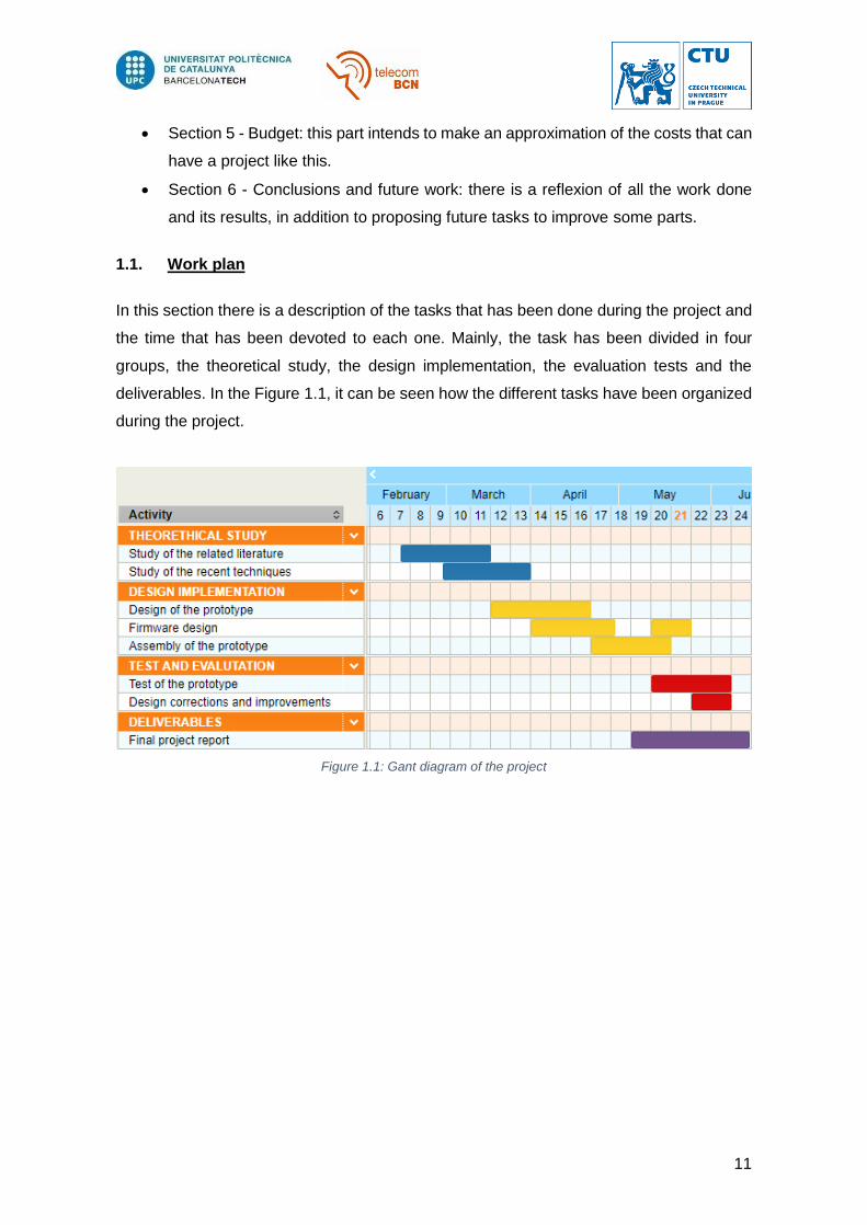
1.1. Work plan
In this section there is a description of the tasks that has been done during the project and
the time that has been devoted to each one. Mainly, the task has been divided in four
groups, the theoretical study, the design implementation, the evaluation tests and the
deliverables. In the Figure 1.1, it can be seen how the different tasks have been organized
during the project.
Figure 1.1: Gant diagram of the project

12
2. State of the art of the technology used or applied in this
thesis
2.1. Introduction
In this section will be a description of the study done of the different techniques for the
implementation of the project. The study will contain the analysis of the transducers
behaviour and the consequent study of the methods for the design of an ultrasonic
generator in order to obtain a functional prototype.
2.2. Ultrasonic transducer modelling
Understanding the characteristics of piezoelectric transducers enables to improve the
performance of ultrasonic systems. In this section, it is intended to explain the modelling
done in this project to ultrasonic transducers in order to obtain a good characterization for
the later designs.
The transducer study can be done based on the Butterworth-Van Dyke, which is very useful
to evaluate overall performances of the ultrasonic transducers. In the Figure 2.1, it can be
seen the equivalent circuit of the model where the mechanical parameters has been
changed to equivalent electrical parameters. R1 reflects the mechanical dissipations, L1
the mass and C1 the flexibility [1].
The impedance of the circuit above is given by:
𝑍𝑇 = 𝑅1 + 𝑗𝜔𝐿1 − 𝑗
1
𝜔𝐶1= ⋯ =
(𝐿1𝐶1𝜔2 − 1) − 𝑗(𝑅1𝐶1𝜔)
𝑅1𝐶𝑝𝐶1𝜔2 + 𝑗[𝐿1𝐶𝑝𝐶1𝜔3 − 𝜔(𝐶𝑝 + 𝐶1)]
eq. 2.1
Figure 2.1: Transducer equivalent circuit
13
If the input signal to the transducer is working at the mechanical resonance frequency of
the piezoelectric element, then the branch formed by R1,L1 and C1 behaves as a purely
resistive load R1.
𝑓𝑚 =
1
2𝜋√𝐿1𝐶1
eq. 2.2
𝑍𝑇|𝜔=𝜔𝑚
=𝑅1
1 + 𝑗𝜔𝑚𝑅1𝐶𝑝
eq. 2.3
From the equations 2.4 and 2.5, it can be extracted the values of R1 and Cp by:
𝑅1 =
|𝑍𝑇|𝜔=𝜔𝑚|2
𝑅𝑒𝑍𝑇|𝜔=𝜔𝑚
eq. 2.4
𝐶𝑝 =
−𝐼𝑚𝑍𝑇|𝜔=𝜔𝑚
2𝜋𝑓𝑚|𝑍𝑇|𝜔=𝜔𝑚|2
eq. 2.5
So giving values to the components of the impedance finally the circuit can be simplified
as a resistance and a reactance at the resonance frequency.
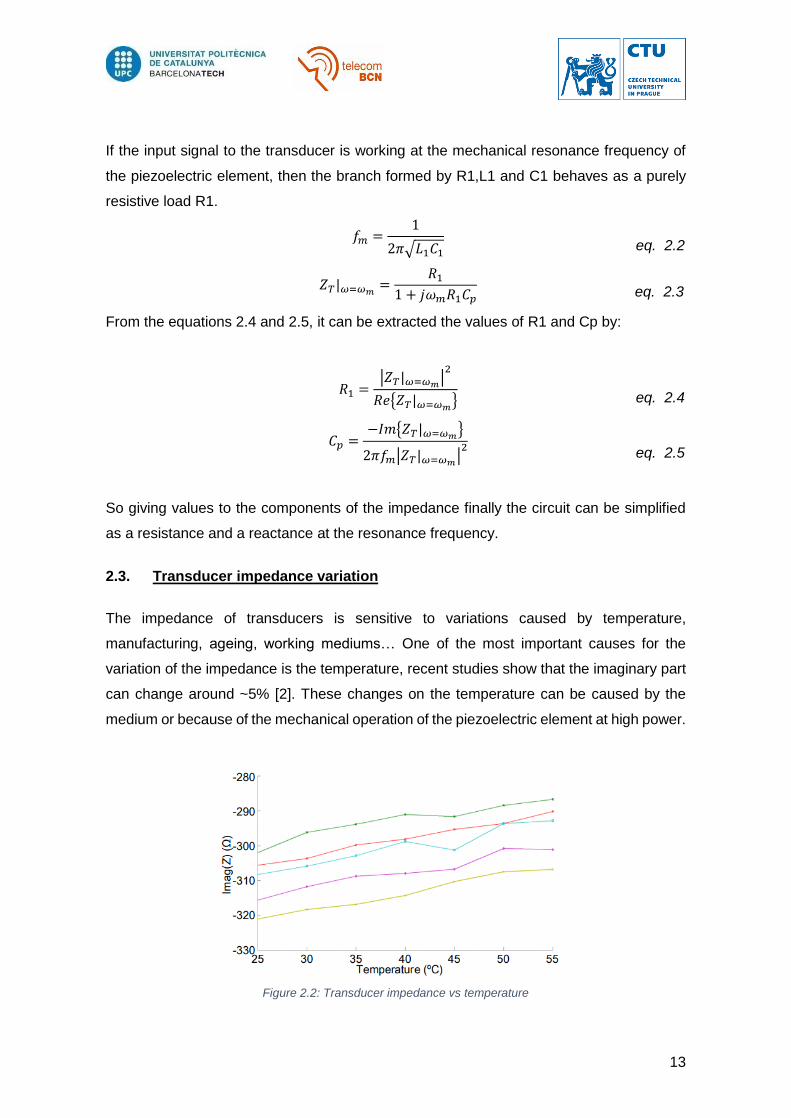
2.3. Transducer impedance variation
The impedance of transducers is sensitive to variations caused by temperature,
manufacturing, ageing, working mediums… One of the most important causes for the
variation of the impedance is the temperature, recent studies show that the imaginary part
can change around ~5% [2]. These changes on the temperature can be caused by the
medium or because of the mechanical operation of the piezoelectric element at high power.
Figure 2.2: Transducer impedance vs temperature
14
Another cause of variation of the dispersions caused in the manufacturing process or the
ageing of the transducers. These variations can reach values about 25-35% of the
imaginary part. These changes in the impedance can produce a detuning of the matching
network that will became in a deterioration of the output power efficiency. In the next section
will be analysed different impedance matching techniques in order to tune the transducer
and maximize the output power.
2.4. Power amplification techniques
One of the most important parts when designing this type of devices is the amplification
stage in order to transfer the desired amount of power to the transducer. In this section a
review of some different power amplification techniques will be done and the selected one
for the project will be explained more accurately.
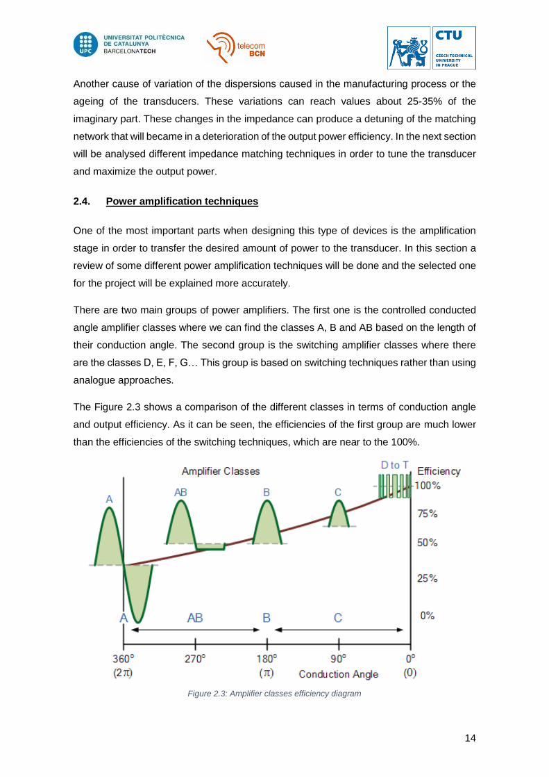
There are two main groups of power amplifiers. The first one is the controlled conducted
angle amplifier classes where we can find the classes A, B and AB based on the length of
their conduction angle. The second group is the switching amplifier classes where there
are the classes D, E, F, G… This group is based on switching techniques rather than using
analogue approaches.
The Figure 2.3 shows a comparison of the different classes in terms of conduction angle
and output efficiency. As it can be seen, the efficiencies of the first group are much lower
than the efficiencies of the switching techniques, which are near to the 100%.
Figure 2.3: Amplifier classes efficiency diagram

15
2.4.1. Controlled conduction angle amplifiers
Class A amplifier
The class A amplifier is the simpler implementation. It has a very good linearity but a very
low power efficiency. In this method, the current flows over the transistor in the whole
waveform cycle. It produces a loss of power and overheating which can be dangerous for
the circuits. One advantage of this amplifier is that it has not crossover distortion problems
like as it could be seen in classes B and AB [3].
The efficiency of this type of amplifiers is about 25-30%, which makes this option not very
attractive, apart from the heating problems, which demands for some cooling facility in
order to not damage the circuits.
Class B amplifier
The class B amplifier is conducting a half of the cycle. It uses two complementary
transistors in order to amplify the opposite halves of the input signal, which is then
recombined at the output. This method achieves an improvement of the efficiency but it
has a drawback that happens in the join of the two halves, where a small mismatch in the
crossover region creates a distortion in the output signal.
This method can obtain a maximum efficiency of 78.5% reducing the heating problem of
the class A amplifier, but the crossover distortion that appears in the output signal makes
this option maybe not the best one.
Class AB
The class AB amplifier, as its name says, has a conduction angle between the class A and
the class B amplifiers. It is a variation of the class B amplifier allowing the two transistors
to conduct at the same time around the crossover point in order to minimize or eliminate
the crossover distortion [3].
This amplifier sacrifices some efficiency in order to obtain a greater linearity in the ouput
signal. The efficiencies that can be obtained with this kind of amplifier are below the
efficiencies of class B amplifiers, typically values between 60-65%.
16
2.4.2. Switching amplifiers
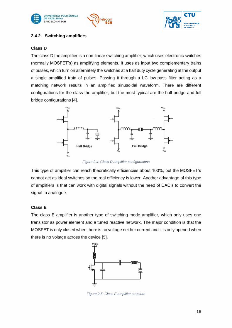
Class D
The class D the amplifier is a non-linear switching amplifier, which uses electronic switches
(normally MOSFET’s) as amplifying elements. It uses as input two complementary trains
of pulses, which turn on alternately the switches at a half duty cycle generating at the output
a single amplified train of pulses. Passing it through a LC low-pass filter acting as a
matching network results in an amplified sinusoidal waveform. There are different
configurations for the class the amplifier, but the most typical are the half bridge and full
bridge configurations [4].
This type of amplifier can reach theoretically efficiencies about 100%, but the MOSFET’s
cannot act as ideal switches so the real efficiency is lower. Another advantage of this type
of amplifiers is that can work with digital signals without the need of DAC’s to convert the
signal to analogue.
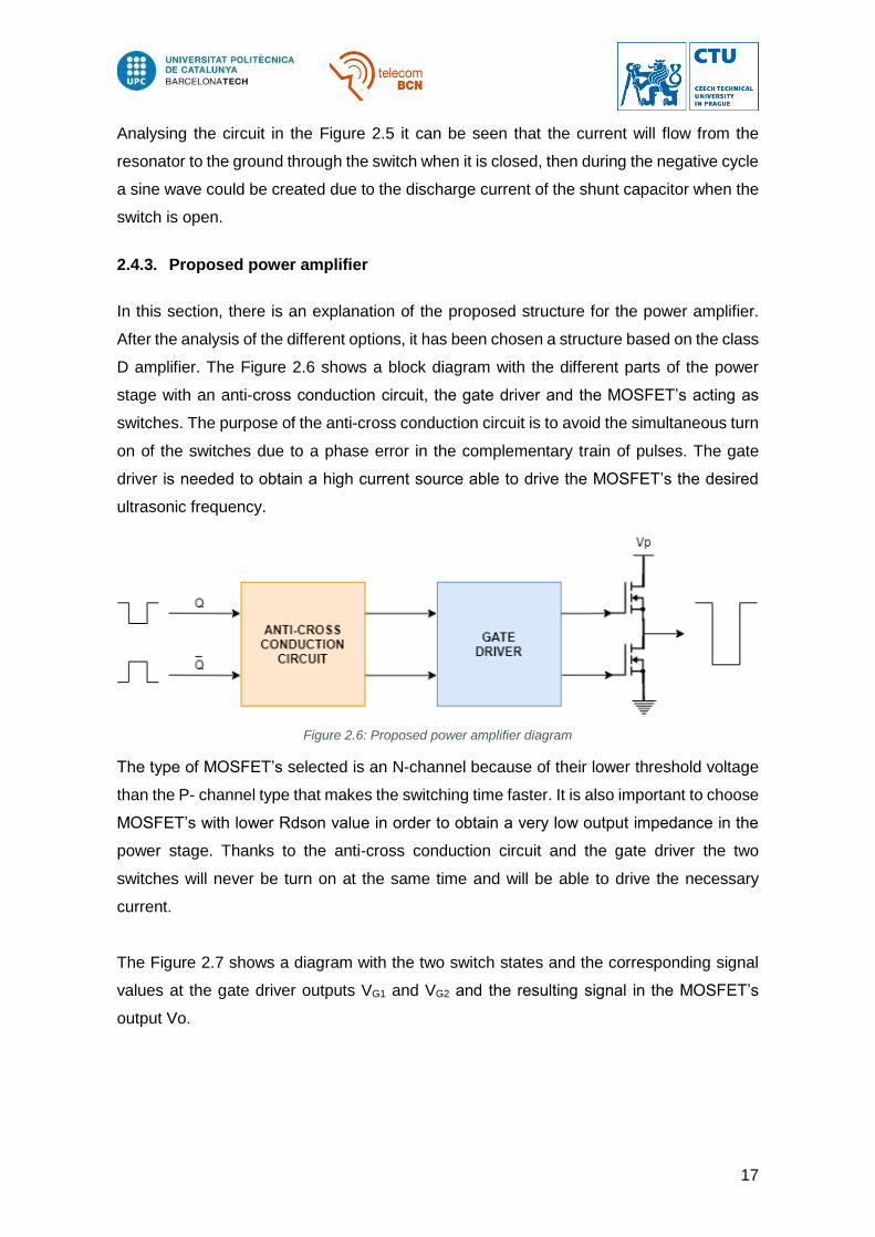
Class E
The class E amplifier is another type of switching-mode amplifier, which only uses one
transistor as power element and a tuned reactive network. The major condition is that the
MOSFET is only closed when there is no voltage neither current and it is only opened when
there is no voltage across the device [5].
Figure 2.5: Class E amplifier structure
Figure 2.4: Class D amplifier configurations
17
Analysing the circuit in the Figure 2.5 it can be seen that the current will flow from the
resonator to the ground through the switch when it is closed, then during the negative cycle
a sine wave could be created due to the discharge current of the shunt capacitor when the
switch is open.
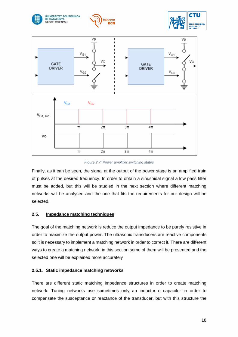
2.4.3. Proposed power amplifier
In this section, there is an explanation of the proposed structure for the power amplifier.
After the analysis of the different options, it has been chosen a structure based on the class
D amplifier. The Figure 2.6 shows a block diagram with the different parts of the power
stage with an anti-cross conduction circuit, the gate driver and the MOSFET’s acting as
switches. The purpose of the anti-cross conduction circuit is to avoid the simultaneous turn
on of the switches due to a phase error in the complementary train of pulses. The gate
driver is needed to obtain a high current source able to drive the MOSFET’s the desired
ultrasonic frequency.
Figure 2.6: Proposed power amplifier diagram
The type of MOSFET’s selected is an N-channel because of their lower threshold voltage
than the P- channel type that makes the switching time faster. It is also important to choose
MOSFET’s with lower Rdson value in order to obtain a very low output impedance in the
power stage. Thanks to the anti-cross conduction circuit and the gate driver the two
switches will never be turn on at the same time and will be able to drive the necessary
current.
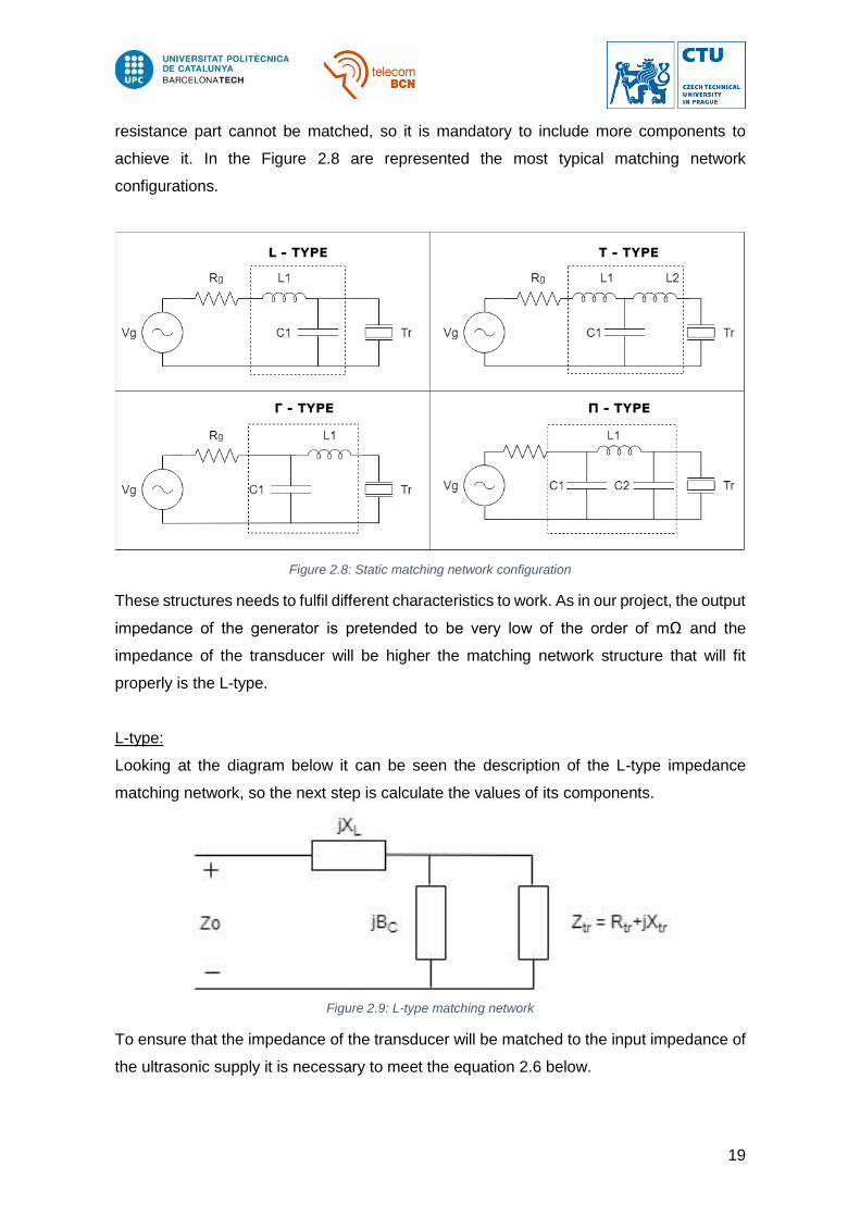
The Figure 2.7 shows a diagram with the two switch states and the corresponding signal
values at the gate driver outputs VG1 and VG2 and the resulting signal in the MOSFET’s
output Vo.
18
Figure 2.7: Power amplifier switching states
Finally, as it can be seen, the signal at the output of the power stage is an amplified train
of pulses at the desired frequency. In order to obtain a sinusoidal signal a low pass filter
must be added, but this will be studied in the next section where different matching
networks will be analysed and the one that fits the requirements for our design will be
selected.
2.5. Impedance matching techniques
The goal of the matching network is reduce the output impedance to be purely resistive in
order to maximize the output power. The ultrasonic transducers are reactive components
so it is necessary to implement a matching network in order to correct it. There are different
ways to create a matching network, in this section some of them will be presented and the
selected one will be explained more accurately
2.5.1. Static impedance matching networks
There are different static matching impedance structures in order to create matching
network. Tuning networks use sometimes only an inductor o capacitor in order to
compensate the susceptance or reactance of the transducer, but with this structure the
19
resistance part cannot be matched, so it is mandatory to include more components to
achieve it. In the Figure 2.8 are represented the most typical matching network
configurations.
Figure 2.8: Static matching network configuration
These structures needs to fulfil different characteristics to work. As in our project, the output
impedance of the generator is pretended to be very low of the order of mΩ and the
impedance of the transducer will be higher the matching network structure that will fit
properly is the L-type.
L-type:
Looking at the diagram below it can be seen the description of the L-type impedance
matching network, so the next step is calculate the values of its components.
Figure 2.9: L-type matching network
To ensure that the impedance of the transducer will be matched to the input impedance of
the ultrasonic supply it is necessary to meet the equation 2.6 below.
20
𝑍0 = 𝑗𝑋𝐿 +
𝑍𝑡𝑟
𝑗𝐵𝑐 · 𝑍𝑡𝑟 + 1= 𝑗𝑋𝐿 +
(𝑅𝑡𝑟 + 𝑗𝑋𝑡𝑟)
𝑗𝐵𝑐 · (𝑅𝑡𝑟 + 𝑗𝑋𝑡𝑟) + 1 eq. 2.6
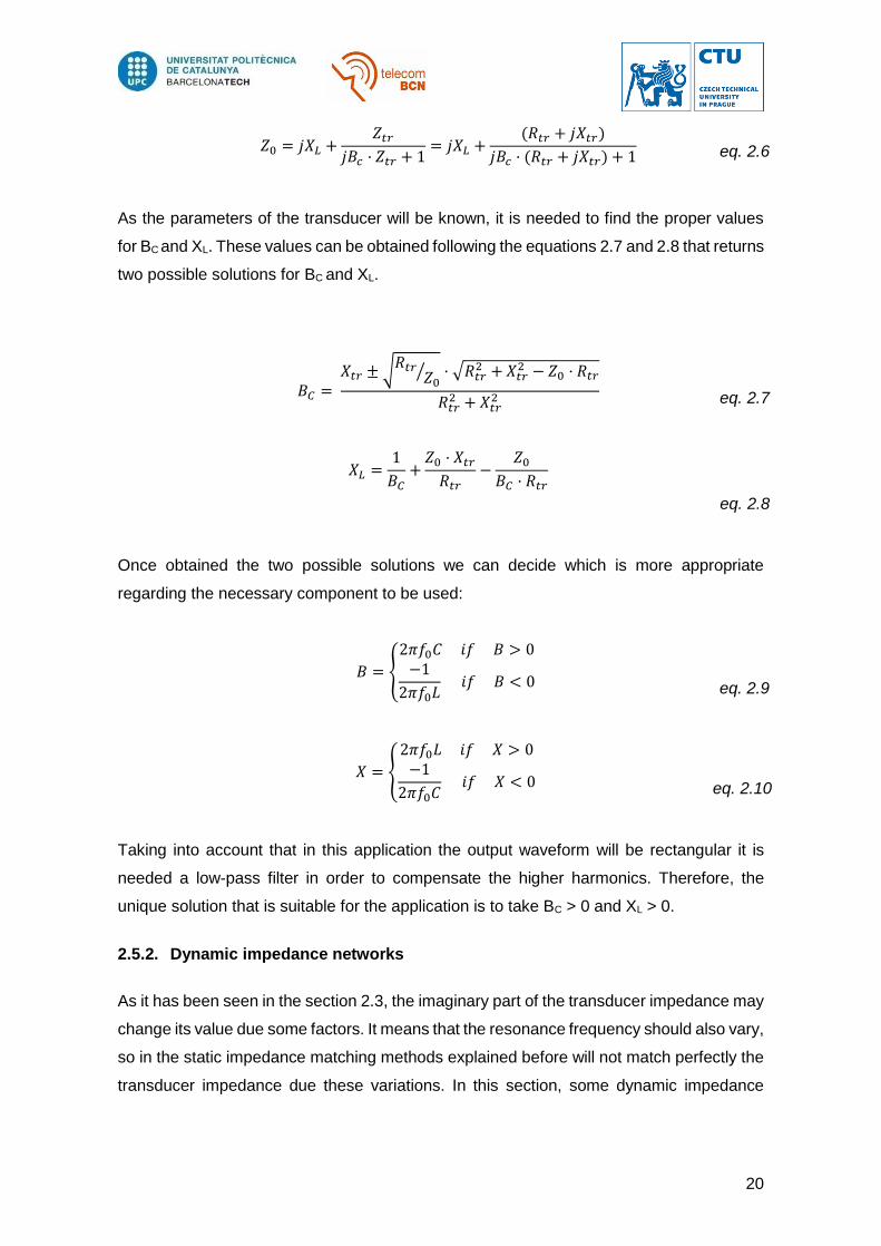
As the parameters of the transducer will be known, it is needed to find the proper values
for BC and XL. These values can be obtained following the equations 2.7 and 2.8 that returns
two possible solutions for BC and XL.
𝐵𝐶 = 𝑋𝑡𝑟 ± √𝑅𝑡𝑟
𝑍0⁄ · √𝑅𝑡𝑟
2 + 𝑋𝑡𝑟2 − 𝑍0 · 𝑅𝑡𝑟
𝑅𝑡𝑟2 + 𝑋𝑡𝑟
2 eq. 2.7
𝑋𝐿 =1
𝐵𝐶+
𝑍0 · 𝑋𝑡𝑟
𝑅𝑡𝑟−
𝑍0
𝐵𝐶 · 𝑅𝑡𝑟
eq. 2.8
Once obtained the two possible solutions we can decide which is more appropriate
regarding the necessary component to be used:
𝐵 =
2𝜋𝑓0𝐶 𝑖𝑓 𝐵 > 0−1
2𝜋𝑓0𝐿 𝑖𝑓 𝐵 < 0
eq. 2.9
𝑋 =
2𝜋𝑓0𝐿 𝑖𝑓 𝑋 > 0−1
2𝜋𝑓0𝐶 𝑖𝑓 𝑋 < 0
eq. 2.10
Taking into account that in this application the output waveform will be rectangular it is
needed a low-pass filter in order to compensate the higher harmonics. Therefore, the
unique solution that is suitable for the application is to take BC > 0 and XL > 0.
2.5.2. Dynamic impedance networks
As it has been seen in the section 2.3, the imaginary part of the transducer impedance may
change its value due some factors. It means that the resonance frequency should also vary,
so in the static impedance matching methods explained before will not match perfectly the
transducer impedance due these variations. In this section, some dynamic impedance

21
networks will be explained in order to match accurately the resonance frequency in the
different conditions.
The first possibility could be the usage of an L-type structure with a variable capacitor in
order to compensate the changes in the imaginary part of the transducer. The capacitance
may be modified changing the distance between the capacitor plates or also changing the
superficial area percentage between them. The problem of this method is that the
capacitance accuracy is very bad because of the mechanical control. The usage of
varactors could be also an option but it has the limitation that the output power would be
limited by the break down voltage of the varactor diode [6].
Another method could be the usage of a set of series/parallel capacitors bypassed by
switches in order to control the necessary filter configuration. It needs some controller in
order to obtain feedback measurements to see if the matching network is fine or must be
modified and also to control the bypass switches. This technique allows obtaining different
filter configurations in order to be as close as possible to the resonance frequency of the
transducer. The technique has the same accuracy problems in the capacitance adjustment
due to the multiple but fixed configurations [7].
Figure 2.10: Bypassed capacitors diagram
22
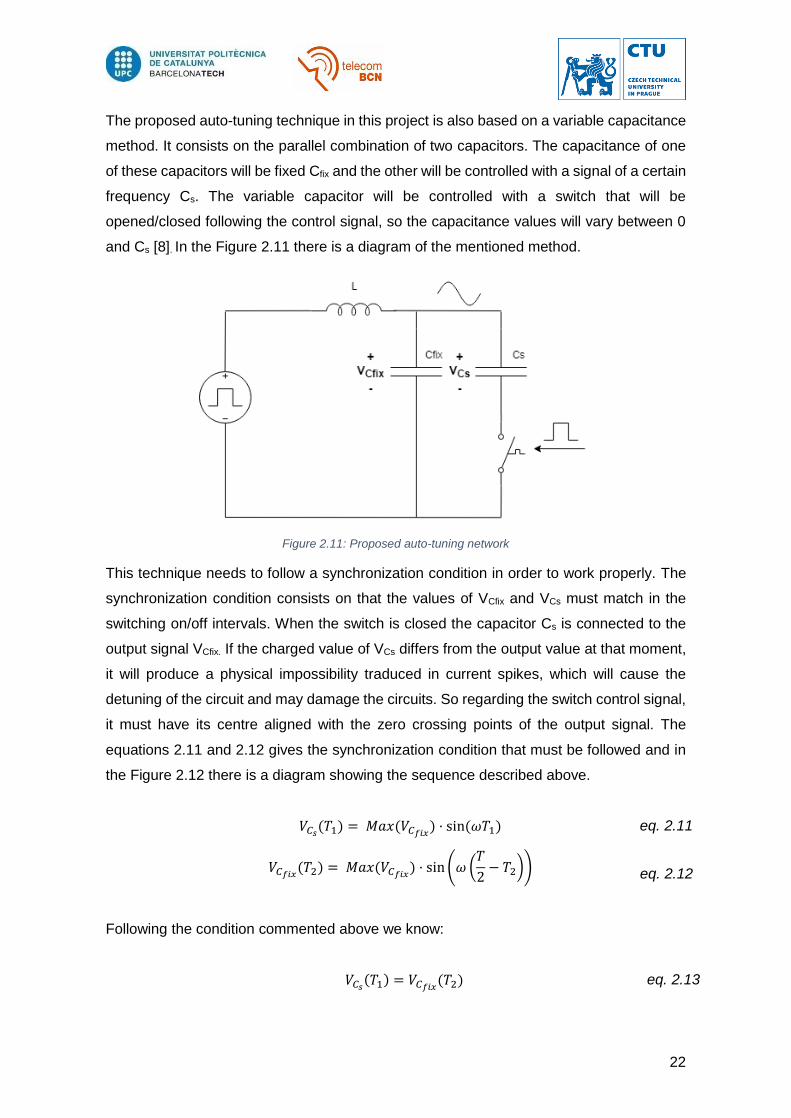
The proposed auto-tuning technique in this project is also based on a variable capacitance
method. It consists on the parallel combination of two capacitors. The capacitance of one
of these capacitors will be fixed Cfix and the other will be controlled with a signal of a certain
frequency Cs. The variable capacitor will be controlled with a switch that will be
opened/closed following the control signal, so the capacitance values will vary between 0
and Cs [8]. In the Figure 2.11 there is a diagram of the mentioned method.
This technique needs to follow a synchronization condition in order to work properly. The
synchronization condition consists on that the values of VCfix and VCs must match in the
switching on/off intervals. When the switch is closed the capacitor Cs is connected to the
output signal VCfix. If the charged value of VCs differs from the output value at that moment,
it will produce a physical impossibility traduced in current spikes, which will cause the
detuning of the circuit and may damage the circuits. So regarding the switch control signal,
it must have its centre aligned with the zero crossing points of the output signal. The
equations 2.11 and 2.12 gives the synchronization condition that must be followed and in
the Figure 2.12 there is a diagram showing the sequence described above.
𝑉𝐶𝑠(𝑇1) = 𝑀𝑎𝑥(𝑉𝐶𝑓𝑖𝑥
) · sin (𝜔𝑇1) eq. 2.11
𝑉𝐶𝑓𝑖𝑥
(𝑇2) = 𝑀𝑎𝑥(𝑉𝐶𝑓𝑖𝑥) · sin (𝜔 (
𝑇
2− 𝑇2)) eq. 2.12
Following the condition commented above we know:
𝑉𝐶𝑠(𝑇1) = 𝑉𝐶𝑓𝑖𝑥
(𝑇2) eq. 2.13
Figure 2.11: Proposed auto-tuning network

23
So finally, we obtain the condition:
𝑇1 =
𝑇
2− 𝑇2 eq. 2.14
Figure 2.12: Switching capacitor signals description
Finally, the equivalent capacitance of the switched capacitor will be determined by the
following equation:
𝐶𝑒𝑞 =
𝛥𝑄
𝛥𝑉𝐶𝑠
eq. 2.15
Where ΔQ is the electrical charge transferred to Cs during the conduction time of the switch
and ΔVCs is the voltage during the same period.
24
3. Methodology / project development
In the previous sections, the project has been placed in context and the theoretical
information needed has been explained. This section will explain the methodology that has
been followed to design and assemble the prototype. The section will be divided mainly in
two parts, hardware and firmware, that will be explained accurately to understand the
techniques used to achieve the project goals.
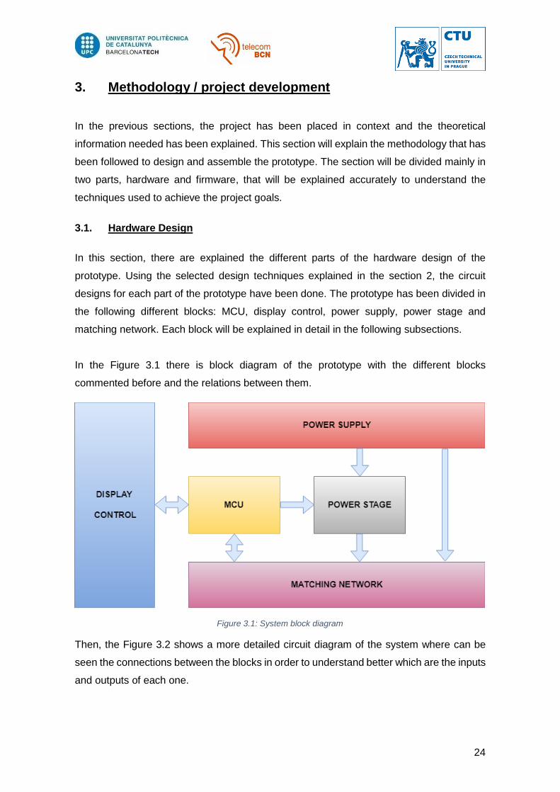
3.1. Hardware Design
In this section, there are explained the different parts of the hardware design of the
prototype. Using the selected design techniques explained in the section 2, the circuit
designs for each part of the prototype have been done. The prototype has been divided in
the following different blocks: MCU, display control, power supply, power stage and
matching network. Each block will be explained in detail in the following subsections.
In the Figure 3.1 there is block diagram of the prototype with the different blocks
commented before and the relations between them.
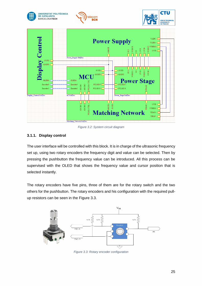
Then, the Figure 3.2 shows a more detailed circuit diagram of the system where can be
seen the connections between the blocks in order to understand better which are the inputs
and outputs of each one.
Figure 3.1: System block diagram
25
Figure 3.2: System circuit diagram
3.1.1. Display control
The user interface will be controlled with this block. It is in charge of the ultrasonic frequency
set up, using two rotary encoders the frequency digit and value can be selected. Then by
pressing the pushbutton the frequency value can be introduced. All this process can be
supervised with the OLED that shows the frequency value and cursor position that is
selected instantly.
The rotary encoders have five pins, three of them are for the rotary switch and the two
others for the pushbutton. The rotary encoders and his configuration with the required pull-
up resistors can be seen in the Figure 3.3.
Figure 3.3: Rotary encoder configuration

26
The OLED display selected in this project is the OLED UG-2864HLBEG01, which uses an
I2C interface for the communication with the MCU [9]. The display has a resolution of
128x64 pixels with different operation modes available by changing the set up configuration.
In the Figure 3.4 it can be seen the OLED display and his pin distribution that will match
with the commented I2C bus used in the MCU section.
3.1.2. Development board (MCU)
The MCU block contains the micro-controller which is the one in charge to configure the
different peripherals and control the development of the application. The chosen MCU for
this project is the development board LAUNCHXL-F28379D from Texas Instruments. This
DSP board has been chosen because of its features that fit the requirements needed for
the project. The supply of the board is done via a USB connector, which is used also for
programming/debugging using a JTAG interface. The system has two cores to work in
parallel with a system clock for each one that works at 20 MHz, more than sufficient for our
application. The requirements for the project are the generation of PWM’s with frequencies
up to 100 kHz, I2C bus interface to control some peripherals, ADC inputs for the feedback
signals, GPIO inputs and interruption control. The selected development board has all
these features to achieve this goal, it provides three dual PWM ports, four ADC’s, two I2C’s
buses and five external interrupt sources, apart from other peripherals which are not
interesting for this application [10]. In the Figure 3.5, it can be seen the description of the
board peripherals.
Figure 3.4: OLED display
Figure 3.5: LAUNCHXL-F28379D pin description
27
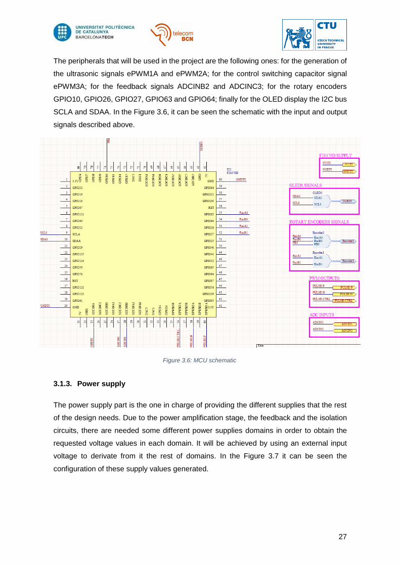
The peripherals that will be used in the project are the following ones: for the generation of
the ultrasonic signals ePWM1A and ePWM2A; for the control switching capacitor signal
ePWM3A; for the feedback signals ADCINB2 and ADCINC3; for the rotary encoders
GPIO10, GPIO26, GPIO27, GPIO63 and GPIO64; finally for the OLED display the I2C bus
SCLA and SDAA. In the Figure 3.6, it can be seen the schematic with the input and output
signals described above.
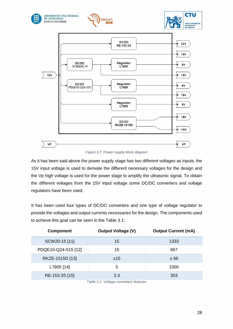
3.1.3. Power supply
The power supply part is the one in charge of providing the different supplies that the rest
of the design needs. Due to the power amplification stage, the feedback and the isolation
circuits, there are needed some different power supplies domains in order to obtain the
requested voltage values in each domain. It will be achieved by using an external input
voltage to derivate from it the rest of domains. In the Figure 3.7 it can be seen the
configuration of these supply values generated.
Figure 3.6: MCU schematic
28
As it has been said above the power supply stage has two different voltages as inputs, the
15V input voltage is used to derivate the different necessary voltages for the design and
the Vp high voltage is used for the power stage to amplify the ultrasonic signal. To obtain
the different voltages from the 15V input voltage some DC/DC converters and voltage
regulators have been used.
It has been used four types of DC/DC converters and one type of voltage regulator to
provide the voltages and output currents necessaries for the design. The components used
to achieve this goal can be seen in the Table 3.1:
Component Output Voltage (V) Output Current (mA)
SCW20-15 [11] 15 1333
PDQE10-Q24-S15 [12] 15 667
RKZE-1515D [13] ±15 ± 66
L7805 [14] 5 1000
RE-153.3S [15] 3.3 303
Table 3.1: Voltage converters features
Figure 3.7: Power supply block diagram

29
The Figure 3.8 shows the circuit design of the power supply stage containing the different
components named above with their recommended filters and decoupling capacitors.
Figure 3.8: Power supply schematic
Finally, the Figure 3.9 shows the power input supplies used and the board design
implemented to achieve the different necessary voltages. As it can be seen in the image
the board is supplied using an external power supply.
Figure 3.9: Power supply board
30
3.1.4. Power stage
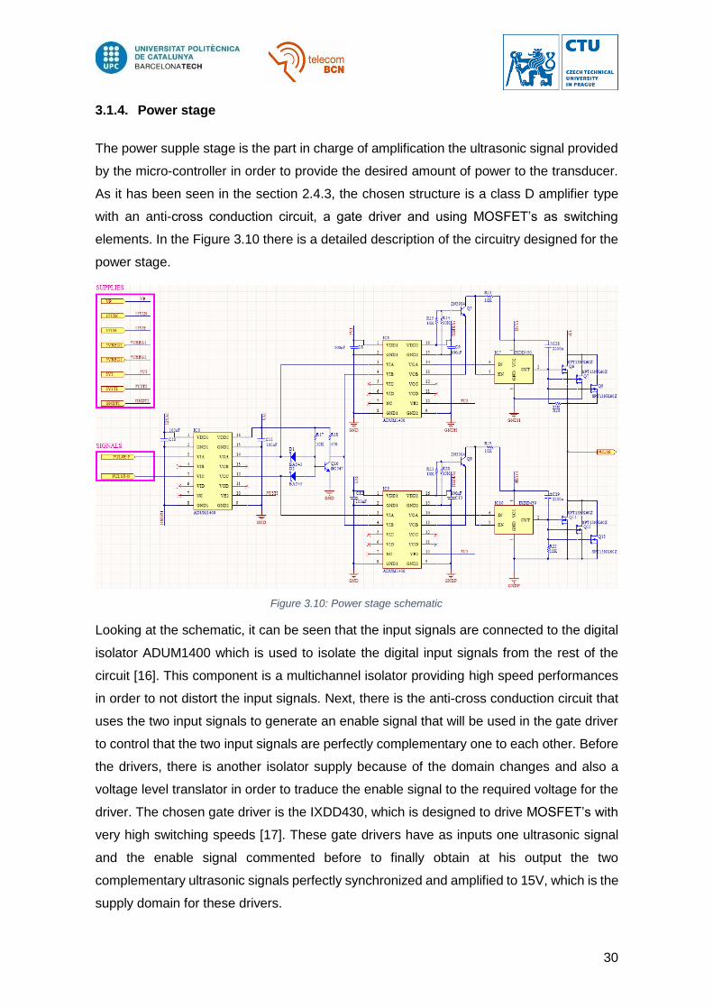
The power supple stage is the part in charge of amplification the ultrasonic signal provided
by the micro-controller in order to provide the desired amount of power to the transducer.
As it has been seen in the section 2.4.3, the chosen structure is a class D amplifier type
with an anti-cross conduction circuit, a gate driver and using MOSFET’s as switching
elements. In the Figure 3.10 there is a detailed description of the circuitry designed for the
power stage.
Looking at the schematic, it can be seen that the input signals are connected to the digital
isolator ADUM1400 which is used to isolate the digital input signals from the rest of the
circuit [16]. This component is a multichannel isolator providing high speed performances
in order to not distort the input signals. Next, there is the anti-cross conduction circuit that
uses the two input signals to generate an enable signal that will be used in the gate driver
to control that the two input signals are perfectly complementary one to each other. Before
the drivers, there is another isolator supply because of the domain changes and also a
voltage level translator in order to traduce the enable signal to the required voltage for the
driver. The chosen gate driver is the IXDD430, which is designed to drive MOSFET’s with
very high switching speeds [17]. These gate drivers have as inputs one ultrasonic signal
and the enable signal commented before to finally obtain at his output the two
complementary ultrasonic signals perfectly synchronized and amplified to 15V, which is the
supply domain for these drivers.
Figure 3.10: Power stage schematic
31
Finally, the last step is connect the two signals to the MOSFET’s acting as switches. As
the required output impedance of power stage must be very low in order to improve the
power efficiency, it has been chosen to connect three N-channel type MOSFET’s in parallel
to implement every switch. The chosen MOSFET is the STP13NK60Z which has a Rdson
equal to 0.48Ω, but with the parallel configuration the output impedance of the power stage
is reduced to 0.16Ω [18]. At the output of the switches, it is obtained an amplified train of
pulses at the ultrasonic frequency selected by the micro-controller with a gain selected by
the voltage Vp which is provided by an external supply.
3.1.5. Impedance study
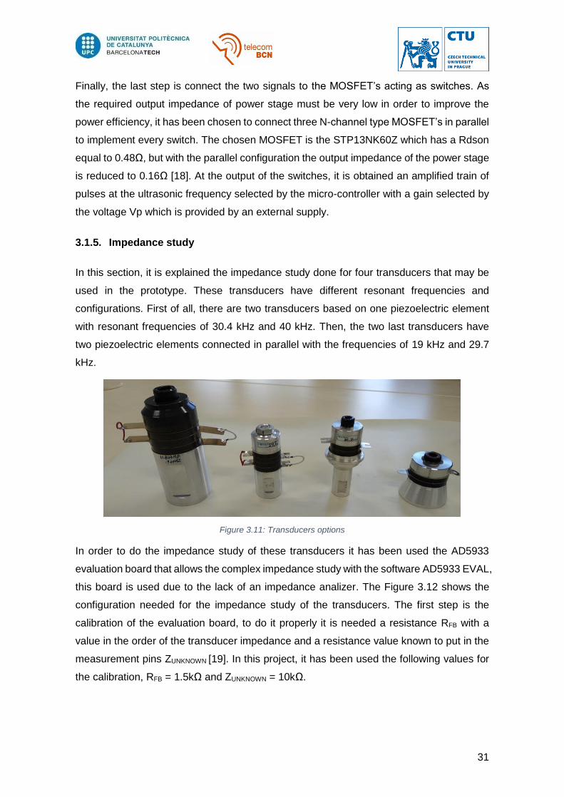
In this section, it is explained the impedance study done for four transducers that may be
used in the prototype. These transducers have different resonant frequencies and
configurations. First of all, there are two transducers based on one piezoelectric element
with resonant frequencies of 30.4 kHz and 40 kHz. Then, the two last transducers have
two piezoelectric elements connected in parallel with the frequencies of 19 kHz and 29.7
kHz.
In order to do the impedance study of these transducers it has been used the AD5933
evaluation board that allows the complex impedance study with the software AD5933 EVAL,
this board is used due to the lack of an impedance analizer. The Figure 3.12 shows the
configuration needed for the impedance study of the transducers. The first step is the
calibration of the evaluation board, to do it properly it is needed a resistance RFB with a
value in the order of the transducer impedance and a resistance value known to put in the
measurement pins ZUNKNOWN [19]. In this project, it has been used the following values for
the calibration, RFB = 1.5kΩ and ZUNKNOWN = 10kΩ.
Figure 3.11: Transducers options

32
Figure 3.12: AD5933 configuration
Next, in the software tool, some configuration values must be introduced in order to perform
the calibration. The first parameters corresponds to the sweep, it is necessary to indicate
the starting frequency, the delta increment of the sweep and the number of increments. In
this case, for an accurate measurement is recommended to introduce a little delta
increment with the theoretical resonance frequency in the centre of the sweep to obtain a
high-resolution measurement. In the next block of parameters it must be set the system
clock as external, the output range excitation to 2Vpp, the PGA control gain to X1 and the
calibration impedance to “Resistor only R1” with the value of the known resistor, in this
case 1.5kΩ. Once these values are properly chosen, click the button “Program Device
Registers” to program the sweep parameters into the appropriate on-board registers of the
AD5933 through the I2C interface. Then chose “Multi-Point Frequency Calibration” in the
“Calibration Gain Factor” section and click on the button “ Calculate Gain Factor”. After that,
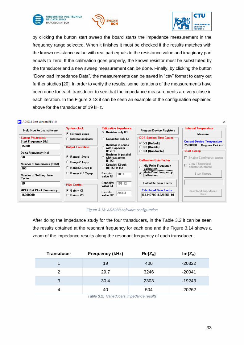
33
by clicking the button start sweep the board starts the impedance measurement in the
frequency range selected. When it finishes it must be checked if the results matches with
the known resistance value with real part equals to the resistance value and imaginary part
equals to zero. If the calibration goes properly, the known resistor must be substituted by
the transducer and a new sweep measurement can be done. Finally, by clicking the button
“Download Impedance Data”, the measurements can be saved in “csv” format to carry out
further studies [20]. In order to verify the results, some iterations of the measurements have
been done for each transducer to see that the impedance measurements are very close in
each iteration. In the Figure 3.13 it can be seen an example of the configuration explained
above for the transducer of 19 kHz.
After doing the impedance study for the four transducers, in the Table 3.2 it can be seen
the results obtained at the resonant frequency for each one and the Figure 3.14 shows a
zoom of the impedance results along the resonant frequency of each transducer.
Transducer Frequency (kHz) ReZtr ImZtr
1 19 400 -20322
2 29.7 3246 -20041
3 30.4 2303 -19243
4 40 504 -20262
Table 3.2: Transducers impedance results
Figure 3.13: AD5933 software configuration

34
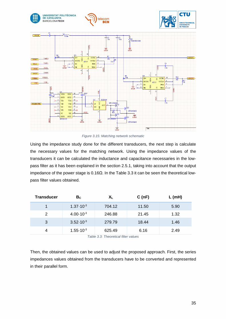
3.1.6. Impedance matching network
In this section it is explained the configuration and the selected values for the components
of the matching network. In the Figure 3.15 it can be seen the proposed strategy structure
explained in the section 2.5.2, which contains a variable capacitor controlled by a switching
signal, a fixed capacitor and an inductor. For the switching capacitor signal, it has been
used and isolator like in the power stage to isolate the digital signal from the rest of the
circuit and also the gate driver IXDD430. In this case, the switching element is composed
by connecting four N-channel type MOSFET’s forming a Totem-Pole configuration. In the
schematic it can also be seen two feedback signals coming from the output of the power
stage and from the transducer, and then going to the ADC’s of the MCU, passing first
through two ADC, to adjust the resonant frequency as it has been explained.
0
5000
10000
15000
20000
25000
30000
25000 27000 29000 31000 33000 35000
29,7 kHz
0
5000
10000
15000
20000
25000
30000
35000
40000
45000
15000 17000 19000 21000 23000 25000
19 kHz
0
10000
20000
30000
40000
50000
60000
70000
80000
35000 37000 39000 41000 43000 45000
40 kHz
0
5000
10000
15000
20000
25000
30000
35000
25000 27000 29000 31000 33000 35000
30,4 kHz
Figure 3.14: Transducers impedance vs frequency
35
Figure 3.15: Matching network schematic
Using the impedance study done for the different transducers, the next step is calculate
the necessary values for the matching network. Using the impedance values of the
transducers it can be calculated the inductance and capacitance necessaries in the low-
pass filter as it has been explained in the section 2.5.1, taking into account that the output
impedance of the power stage is 0.16Ω. In the Table 3.3 it can be seen the theoretical low-
pass filter values obtained.
Transducer BC XL C (nF) L (mH)
1 1.37·10-3 704.12 11.50 5.90
2 4.00·10-3 246.88 21.45 1.32
3 3.52·10-3 279.79 18.44 1.46
4 1.55·10-3 625.49 6.16 2.49
Table 3.3: Theoretical filter values
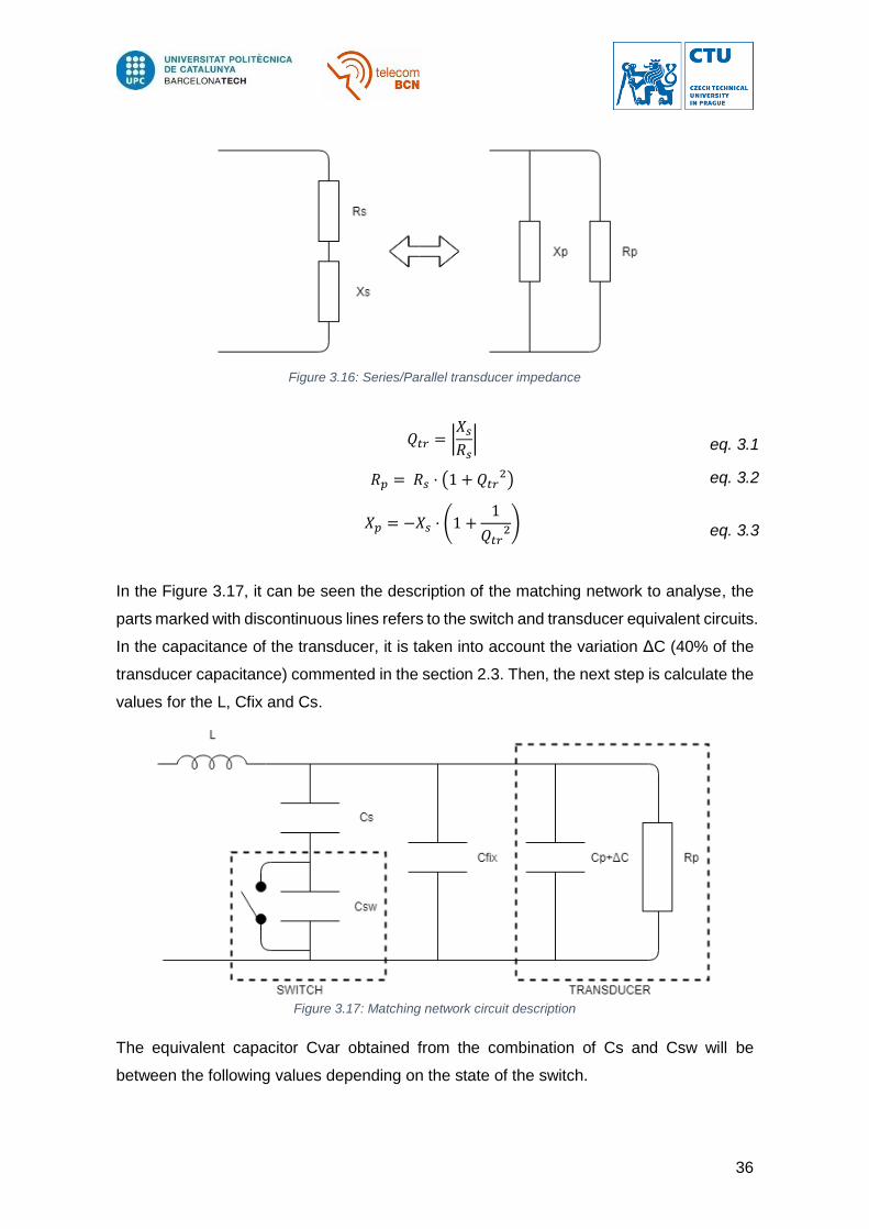
Then, the obtained values can be used to adjust the proposed approach. First, the series
impedances values obtained from the transducers have to be converted and represented
in their parallel form.
36
𝑄𝑡𝑟 = |
𝑋𝑠
𝑅𝑠| eq. 3.1
𝑅𝑝 = 𝑅𝑠 · (1 + 𝑄𝑡𝑟2) eq. 3.2
𝑋𝑝 = −𝑋𝑠 · (1 +
1
𝑄𝑡𝑟2) eq. 3.3
In the Figure 3.17, it can be seen the description of the matching network to analyse, the
parts marked with discontinuous lines refers to the switch and transducer equivalent circuits.
In the capacitance of the transducer, it is taken into account the variation ΔC (40% of the
transducer capacitance) commented in the section 2.3. Then, the next step is calculate the
values for the L, Cfix and Cs.
Figure 3.17: Matching network circuit description
The equivalent capacitor Cvar obtained from the combination of Cs and Csw will be
between the following values depending on the state of the switch.
Figure 3.16: Series/Parallel transducer impedance

37
𝐶𝑠 · 𝐶𝑠𝑤
𝐶𝑠 + 𝐶𝑠𝑤≤ 𝐶𝑣𝑎𝑟 ≤ 𝐶𝑠 eq. 3.4
The Cvar capacitance has to compensate the deviations of the transducer capacitance ΔC.
So, it must follow the next equation.
𝐶𝑠 −𝐶𝑠 · 𝐶𝑠𝑤
𝐶𝑠 + 𝐶𝑠𝑤= ΔC eq. 3.5
Solving the equation 3.5 it can be found the value of Cs, taking as Csw the ouput
capacitance of the switch formed by the 4 NMOS, which have the equivalent capacitance
of one NMOS, Csw = Coss = 210pF [18].
𝐶𝑠2 − ΔC · 𝐶𝑠 − 𝐶𝑠𝑤 · ΔC = 0 eq. 3.6
The next step is to obtain the value of Cfix from the equivalent capacitance and substituting
it into the resonant frequency condition. To obtain a result, would be necessary to use the
inductance value obtained in the impedance study.
𝐶𝑒𝑞 =1
2[𝐶𝑠 +
𝐶𝑠 · 𝐶𝑠𝑤
𝐶𝑠 + 𝐶𝑠𝑤] + 𝐶𝑓𝑖𝑥 + 𝐶𝑝 eq. 3.7
𝑓𝑜 =1
2𝜋√𝐿 · 𝐶𝑒𝑞
eq. 3.8
Substituting the equation 3.7 into the equation 3.8 it is obtain the value of Cfix.
𝐶𝑓𝑖𝑥 =1
(2𝜋𝑓𝑜)2𝐿−
1
2[𝐶𝑠 +
𝐶𝑠 · 𝐶𝑠𝑤
𝐶𝑠 + 𝐶𝑠𝑤] − 𝐶𝑝 eq. 3.9
Therefore, following the procedure explained in this section and using the impedance
values of the Table 3.2. It has been calculated the theoretical and real values of the
matching network for the different transducers. In the Table 3.4 and Table 3.5 there are the
different values obtained for the different variables of the analysis.

38
Transducer fo(kHz)
Cp(pF) ΔC(pF) Cs(pF) Cfix(nF) L(mH)
19 412.0 164.8 285.8 19.9 3.405
29.7 260.5 104.2 208.9 37.2 0.760 30.4 268.2 107.2 213.1 31.9 0.845
40 196.2 78.5 173.5 10.6 1.44 Table 3.4: Theoretical filter components values
Cs(pF) Cfix(nF) L(mH) fo(kHz)
270 20 3.4 19.17 220 37 0.75 30.12
220 32 0.85 30.41 180 10 1.5 40.72
Table 3.5: Real filter components values
Finally, as it has been said at the beginning of this section, there are two feedback signals
that will be used for controlling the resonance frequency of the transducer. To acquire these
signals, it can be seen in the schematic that a potentiometer will be used to attenuate the
output signals and then an isolated amplifier AD215 is used before connecting the signals
with the required voltage range to the ADC’s inputs of the micro-controller [21]. This
feedback control is added because the resonance frequency may not be exactly the ideal
one and can vary due the comment factors.
3.1.7. Prototype assembly
Once the different parts of the circuit have been designed and described, the next step is
the assembly of them. As this is first version of the prototype, it has been decided to use
fiberglass prototype boards to assemble the different blocks of the design. In the Figure
3.18 it can be seen the different boards assembled to obtain the different stages of the
design.
Figure 3.18: Prototype boards

39
The assembly of the different components has been done using connectors in order to
allow the fast change of the components in case of damage. It is also very useful for the
matching network stage the easy change of the components of the filter to adapt it to the
required values.
3.2. Firmware design
This section explains which methodology has been followed to design the firmware and
how has been structured.
The firmware design has been done using the C language, which is used with the
development board LAUNCHXL-F28379D from Texas Instruments [22]. As it has been said
in the hardware design, this development board is a very good choice for DSP applications
and allows many configurations on the input and output pins that make it very versatile. To
achieve the desired configuration, the Code Composer Studio tool based on Eclipse has
been used in order to implement, compile and program the firmware. It is a professional
tool with advanced compiler and debugging options, which are useful for the development
part [23].
The firmware of the application consists on implement the frequency selection, the signal
generation and the frequency control. To achieve it, the firmware starts a main application,
which is in charge to initialize all the peripherals that would be used and to control the
progress of the application in every moment. Below the main application, there are the
following different functionalities: frequency selection, frequency display, signal generation
and frequency adjustment.
Figure 3.19: Firmware block diagram
40
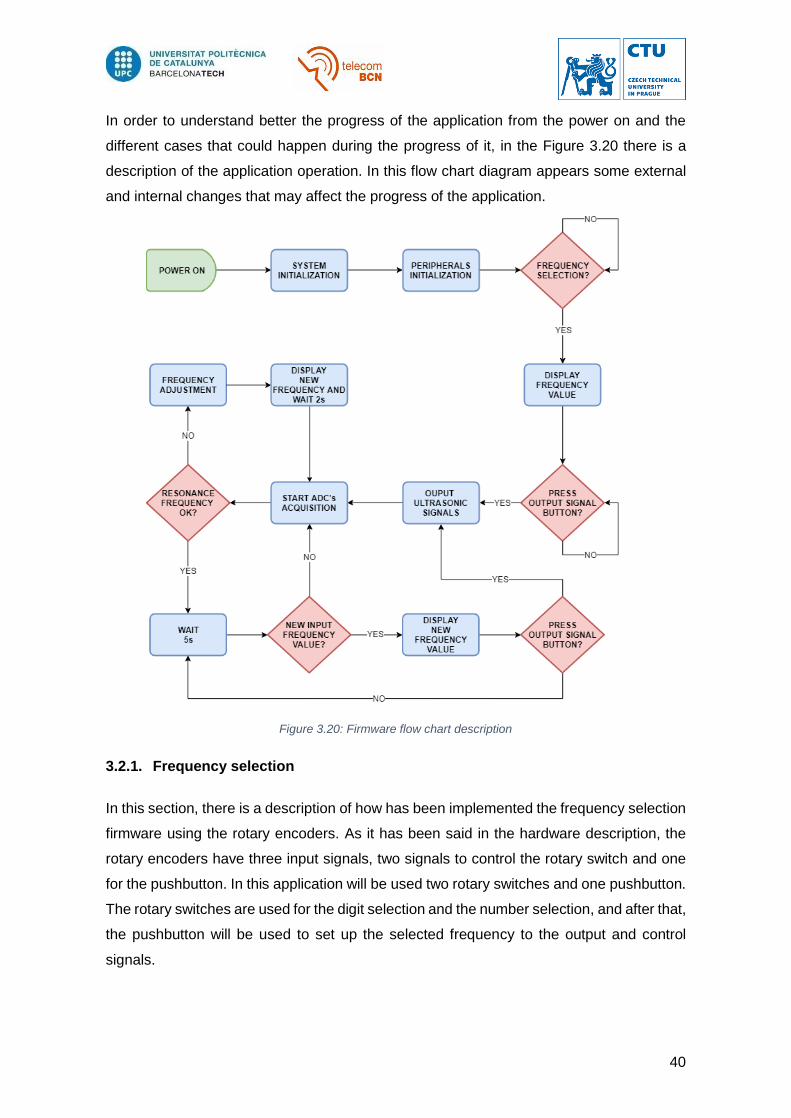
In order to understand better the progress of the application from the power on and the
different cases that could happen during the progress of it, in the Figure 3.20 there is a
description of the application operation. In this flow chart diagram appears some external
and internal changes that may affect the progress of the application.
3.2.1. Frequency selection
In this section, there is a description of how has been implemented the frequency selection
firmware using the rotary encoders. As it has been said in the hardware description, the
rotary encoders have three input signals, two signals to control the rotary switch and one
for the pushbutton. In this application will be used two rotary switches and one pushbutton.
The rotary switches are used for the digit selection and the number selection, and after that,
the pushbutton will be used to set up the selected frequency to the output and control
signals.
Figure 3.20: Firmware flow chart description

41
The application has been designed so that you can change the frequency at any time, so
one of the input pins of each rotary switch and the pushbutton input pin have been
configured as interrupt GPIO’s with falling edge. The Figure 3.21 and Table 3.6 shows the
truth table to interpret the two input signals of the rotary switches when a falling edge is
triggered.
Clockwise Counter Clockwise
PIN A 0 0 PIN B 1 0
Table 3.6: Rotary encoder logic table
It is also necessary that every time the digit cursor or frequency number is changed the
display update it. Therefore, this block is going to call the frequency display block every
time it happens.
3.2.2. Frequency display
The display control block contains the different methods to use the display. It has
implemented the initialization configuration and the methods for displaying text and forms.
As the display used in the design works with an I2C bus, below this service there is also
an I2C driver for the interaction between the display and the microcontroller.
Figure 3.21: Rotary encoder signals description
42
As it has been said in the hardware section, the display used is the OLED UG-
2864HLBEG01, which works with the SSD1306 driver. In this project, the display is used
for showing the frequency of the ultrasonic signal, so the following functionalities has been
done in order to achieve it: the initialization for a resolution of 128x64 dot matrix, reset,
clear, display On/Off, “go to XY” and display text [24]. The display is divided in 4 lines, in
the first line appears the text “Frequency:”, the second line is not used, the third line shows
the frequency value and the last line contains a cursor which indicates the digit selected.
As the maximum frequency to set up would be 100 kHz the display will shows 6 digits for
the frequency value. In the Figure 3.22 it can be seen an example of the display output.
3.2.3. Signal generation
The signal generation block will be in charge of the generation of the ultrasonic signals and
the control signal for the variable capacitor. The ePWM outputs of the Launchpad F28379D
has been used to fulfil this purpose. The board can generate six ePWM signals with two
inverted outputs each one, so in this application ePWM1 and ePWM2 are used for the
ultrasonic signal generation and ePWM3 is used for the variable capacitor control signal.
The two signals must be synchronized between them so they are derived from the system
clock and it is possible to control the phase offset.
In the Figure 3.23 it can be seen the ultrasonic square signal generated for the ePWM1
and the complementary signal generated by the ePWM2. As it can be seen the phase
difference is T/2 and the duty cycle is 50%.
Figure 3.22: Display and rotary encoders
43
Figure 3.23: Ultrasonic complementary signals description
In the Figure 3.24 it can be seen on top the one of the ultrasonic pulses and below the
variable capacitor control pulses with twice the frequency and required phase offset of T/8.
3.2.4. Feedback signals
In this section will be explained the algorithm implemented to do the frequency control using
the input feedback signals coming from the matching network stage. As it can be seen in
the section 3.1.6 the feedback signals comes from the output of the power stage and from
the transducer. Therefore, after adapting this signals to be acquired by the ADC’s of the
micro-controller, it is obtained a train of pulses and a sinusoidal signal after the acquisition.
What pretends the algorithm is to ensure that the resonant frequency point is achieved, so
as it has been commented above, the matching network plus de transducer must behave
as a purely resistive load in the resonance frequency. It means that the phase difference
between these two signals must be zero.
Figure 3.24: Ultrasonic signal and control signal description
44
First of all, the algorithm will acquire the two signals precisely at the same time instance
using the ADC’s synchronized with the micro-controller system clock. Then, it will
determine the period of the two feedback signals that must be the same. The phase
difference of the signals will be computed and a percentage with the signal period will be
extracted following the equation 2.13:
𝜃𝑑𝑖𝑓𝑓(%) =
|𝜃𝑑𝑖𝑓𝑓|
𝑇𝑝𝑒𝑟𝑖𝑜𝑑
eq. 2.13
If the phase difference percentage is greater than the 5%, it will be considered that the
resonance frequency point it is not achieved. Then, the algorithm will increase the output
frequency with an offset value Δf (for example the starting point of this increment can be
around 50Hz) and after that, it will repeat the acquisition process and the phase difference
calculation. If the new phase difference is lower, this process will be repeated again with
the same frequency offset increment until it is obtained a greater phase difference reading
regarding the last measurement. Then, the frequency offset will be divided by two Δf/2 and
subtracted instead of added. The same process as before will be done with the subtraction
of the frequency offset until it is obtained again a greater phase difference. This process is
a converging algorithm that will end when the difference percentage belongs below the 5%.
Then, it will be considered that the frequency resonance has achieved its resonance
frequency point. In the Figure 3.25 there is a graphical description of the algorithm until it
reaches convergence, the frequency changes between each iteration are not illustrated in
the diagram because will be very small, but they are present.
Figure 3.25: Feedback algorithm example
45
As it can be seen in the diagram above, the first iteration computes a phase difference out
of the 5% region allowed, so in the next iteration a Δf increment it is applied. As the phase
difference is reduced in the iteration 2, a new increment with the same frequency offset is
applied. Looking at the iteration 3 it can be seen that now the phase difference has been
incremented, so the algorithm will subtract this time a frequency offset of Δf/2 as it has
been explained. Finally, in the last iteration it can be seen that the phase difference is
between 5% range so the algorithm converges.
During each iteration of the algorithm, if there is a change in the frequency of the output
signal it is reflected instantaneously to the display to make the user able to supervise the
frequency changes until the convergence. Apart from that, the user will be able to change
manually the frequency using the rotary encoders. If it happens all the process explained
above will start again around the new frequency value.
46
4. Results
4.1. Hardware tests
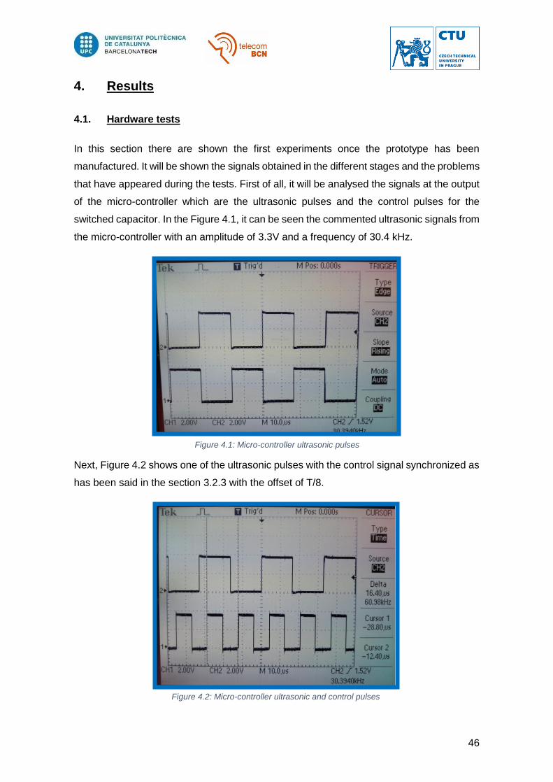
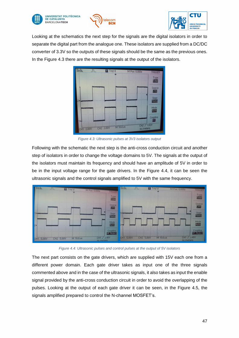
In this section there are shown the first experiments once the prototype has been
manufactured. It will be shown the signals obtained in the different stages and the problems
that have appeared during the tests. First of all, it will be analysed the signals at the output
of the micro-controller which are the ultrasonic pulses and the control pulses for the
switched capacitor. In the Figure 4.1, it can be seen the commented ultrasonic signals from
the micro-controller with an amplitude of 3.3V and a frequency of 30.4 kHz.
Next, Figure 4.2 shows one of the ultrasonic pulses with the control signal synchronized as
has been said in the section 3.2.3 with the offset of T/8.
Figure 4.1: Micro-controller ultrasonic pulses
Figure 4.2: Micro-controller ultrasonic and control pulses
47
Looking at the schematics the next step for the signals are the digital isolators in order to
separate the digital part from the analogue one. These isolators are supplied from a DC/DC
converter of 3.3V so the outputs of these signals should be the same as the previous ones.
In the Figure 4.3 there are the resulting signals at the output of the isolators.
Following with the schematic the next step is the anti-cross conduction circuit and another
step of isolators in order to change the voltage domains to 5V. The signals at the output of
the isolators must maintain its frequency and should have an amplitude of 5V in order to
be in the input voltage range for the gate drivers. In the Figure 4.4, it can be seen the
ultrasonic signals and the control signals amplified to 5V with the same frequency.
The next part consists on the gate drivers, which are supplied with 15V each one from a
different power domain. Each gate driver takes as input one of the three signals
commented above and in the case of the ultrasonic signals, it also takes as input the enable
signal provided by the anti-cross conduction circuit in order to avoid the overlapping of the
pulses. Looking at the output of each gate driver it can be seen, in the Figure 4.5, the
signals amplified prepared to control the N-channel MOSFET’s.
Figure 4.3: Ultrasonic pulses at 3V3 isolators output
Figure 4.4: Ultrasonic pulses and control pulses at the output of 5V isolators

48
The next part will consist on connect the ultrasonic signals from the output of the gate
drivers to the MOSFET’s which have to act as switches to obtain a final single train of
pulses amplified to the voltage Vp. At this part it has been seen that the MOSFET’s do not
act as it was expected so after analysing the circuit and signals, it has been realized that
the input train of pulses from the drivers had noisy oscillations in both edges of the pulses.
It supposes a problem because these oscillations provokes that the MOSFET’s are closed
at the same time for a few moments. This fact provokes a short circuit in the Vp power
supply traduced in very high current spikes which may damage the circuits. In the Figure
4.6, it can be seen the noisy oscillations at the falling edge of the pulses that cause the
malfunction of the MOSFET’s.
At this point, the next step has been trying to identify from where come the oscillations and
try to eliminate it in order to obtain clean train of pulses at the output of the gate drivers.
First, the power supplies of the gate drivers has been analysed and it has been seen that
the oscillations appears also there. The Figure 4.7 shows one output of the gate driver and
its supply where can be seen the noisy effect in both signals at the same moment. The first
Figure 4.5: Ultrasonic and control signals at the gate drivers output
Figure 4.6: Falling edge ringing noise

49
modification done in order to eliminate this effect was to add capacitors with higher values
at the outputs of the power supplies in order to make it more stable. As the solution
commented before does not work it has been tried to change the DC/DC switched power
supplies for linear supplies in order to see if providing a more stable supply to the gate
driver helps in the elimination of noise.
As these solution makes no change it has been analysed again the noisy effect and it has
been concluded that this oscillations could be provoked by some second order circuit, so
in order to reduce the inductance effect of the wiring, it has been reduced their length in
order to obtain cleaner output signals. To achieve it, a new board containing a simplified
power stage has been constructed. In this board the anti-cross conduction circuit has been
deleted and it only contains the isolators, the gate drivers and the MOSFET’s [25].In order
to control the overlap of the signals it has been increased the dead band between them by
the firmware of the micro-controller, because in this test circuit there is no anti-cross
conduction circuit. In the Figure 4.8, it can be seen a block diagram description of the new
test circuit and the obtained signals at the output of the gate drivers.
Figure 4.7: Gate driver supply and output with noisy presence
Figure 4.8: Test circuit block diagram and gate drivers output
50
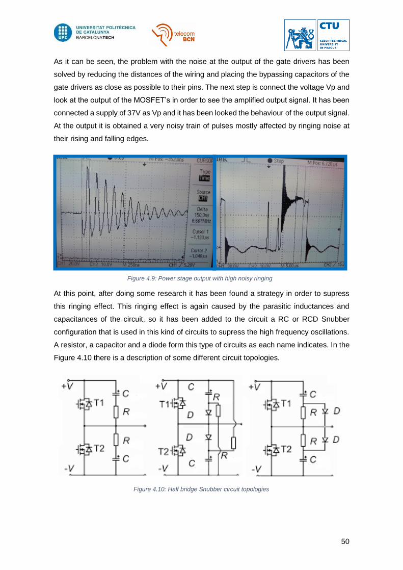
As it can be seen, the problem with the noise at the output of the gate drivers has been
solved by reducing the distances of the wiring and placing the bypassing capacitors of the
gate drivers as close as possible to their pins. The next step is connect the voltage Vp and
look at the output of the MOSFET’s in order to see the amplified output signal. It has been
connected a supply of 37V as Vp and it has been looked the behaviour of the output signal.
At the output it is obtained a very noisy train of pulses mostly affected by ringing noise at
their rising and falling edges.
At this point, after doing some research it has been found a strategy in order to supress
this ringing effect. This ringing effect is again caused by the parasitic inductances and
capacitances of the circuit, so it has been added to the circuit a RC or RCD Snubber
configuration that is used in this kind of circuits to supress the high frequency oscillations.
A resistor, a capacitor and a diode form this type of circuits as each name indicates. In the
Figure 4.10 there is a description of some different circuit topologies.
Figure 4.9: Power stage output with high noisy ringing
Figure 4.10: Half bridge Snubber circuit topologies

51
Before adding this circuit configuration to the N-channel MOSFET’s is necessary to
compute the necessary component values to supress the obtained ringing. In order to do
that in the following equations there are some calculations to obtain these values [26]. First
of all, it is necessary to know the parasitic values Lp and Cp. It has been taken the output
capacitance of the MOSFET as the parasitic capacitance Cp = 1360 pF. Then, it can be
obtained the parasitic inductance of the wires if the ringing frequency is known FRING =
6.67MHz:
𝑓𝑅𝐼𝑁𝐺 =
1
2𝜋√𝐿𝑝 · 𝐶𝑝
eq. 4.1
𝐿𝑝 = 1
(2𝜋𝑓𝑅𝐼𝑁𝐺)2 · 𝐶𝑝= 418.64 𝑛𝐻
eq. 4.2
From these results, it is obtained the value of RS:
𝑅𝑆 = 1
2√
𝐿𝑝
𝐶𝑝= 8.77 Ω
eq. 4.3
The last step is compute de Cs value, taking as cut off frequency FRING:
𝐶𝑠 =
1
2𝜋 · 𝑅𝑠 · 𝑓𝑅𝐼𝑁𝐺= 2.72 𝑛𝐹 eq. 4.4
Once this values has been calculated it has been chosen some real values in order to
implement it. It has been done some tests with the RC simple topology with a resistor of
8Ω and different capacitor values like 2.2nF, 3.3nF… The best results has been obtained
with the 3.3nF capacitor, which has the following cut off frequency:
𝑓𝑐 =
1
2𝜋 · 𝑅𝑠 · 𝐶𝑠≈ 6 𝑀𝐻𝑧 eq. 4.5
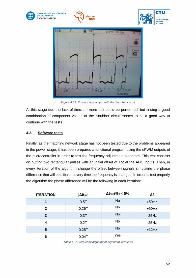
In the Figure 4.11, it can be seen the resulting signal obtained at the output of the power
stage with the Snubber circuit. It is visible that the ringing has decreased so much but there
is still a noisy oscillation with a period of 240ns. It can be seen also that there are still some
noisy impulses between the train of pulses.
52
At this stage due the lack of time, no more test could be performed, but finding a good
combination of component values of the Snubber circuit seems to be a good way to
continue with the tests.
4.2. Software tests
Finally, as the matching network stage has not been tested due to the problems appeared
in the power stage, it has been prepared a functional program using the ePWM outputs of
the microcontroller in order to test the frequency adjustment algorithm. This test consists
on putting two rectangular pulses with an initial offset of T/2 at the ADC inputs. Then, in
every iteration of the algorithm change the offset between signals simulating the phase
difference that will be different every time the frequency is changed. In order to test properly
the algorithm the phase difference will be the following in each iteration:
ITERATION |Δθdiff| Δθdiff(%) < 5% Δf
1 0.5T No +50Hz
2 0.25T No +50Hz
3 0.3T No -25Hz
4 0.2T No -25Hz
5 0.25T No +12Hz
6 0.04T Yes -
Table 4.1: Frequency adjustment algorithm iterations
Figure 4.11: Power stage output with the Snubber circuit

53
As it can be seen in the Table 4.1, the first iteration starts with a phase difference of 0.5T,
so it is added a frequency adjustment offset of 50Hz. In the next iteration, the phase
difference has been reduced so it is added again the same frequency offset. Following with
the next iteration it can be seen that now the phase difference has incremented respect the
last one, so next the frequency offset will be the half than before and subtracted to the
frequency. The next iteration shows again lower phase difference, so it will continue being
subtracted the 25Hz. Following, in the next one, it can be seen again an increment of the
phase difference, then the frequency offset will be divided again by two and added to the
frequency. Finally, in the last iteration it can be seen that the phase difference in percentage
accomplish the 5% range, so it means that the algorithm has converged.
By forcing the commented phase differences in each iteration, it has been checked that the
frequency offset values follow the same logic that has been seen in the table and the
algorithm converges at the expected iteration.

54
5. Budget
In this section there is a small economic balance on the cost trying to illustrate how difficult
can be to assume a project without the help of any organization or company. All projects,
although the final result it is not a physical device, have a cost. In this case, it can be seen
that this project would be difficult to afford without the help of the CTU, who has carried out
with the material costs.
In order to understand better how the costs are broken down, they have been separated
into the prototype, the instrumentation and the working costs. The following tables will show
the description of each part and its corresponding total cost. First of all, the Table 5.1 shows
the cost of the prototype materials that has been used. As it can be seen the components
that raise the price are the micro-controller evaluation board and the isolated amplifiers
which are used for the sampling of the feedback signals. There are also some DC/DC
converters with higher prices, but apart from that, the other components used are
affordable with low prices.
PROTOTYPE COMPONENTS
Name Component Price x
unit(Kc) Price x unit(€)
Units Total(Kc) Total(€)
Power Supply Stage
DC/DC converter SCW20A-15 566,61 Kč 22,22 € 1 566,61 Kč 22,22 €
DC/DC converter PDQE10-Q24-S15-D 359,30 Kč 14,09 € 1 359,30 Kč 14,09 €
DC/DC converter RE153,3S 132,09 Kč 5,18 € 1 132,09 Kč 5,18 €
DC/DC converter dual RKZE-1515D 151,98 Kč 5,96 € 1 151,98 Kč 5,96 €
Voltage regulator L7805 10,71 Kč 0,42 € 3 32,13 Kč 1,26 €
Toggle switch 100SP1T2B1M1QEH 49,98 Kč 1,96 € 1 49,98 Kč 1,96 €
Power Stage
Digital isolator ADUM1400 101,75 Kč 3,99 € 4 406,98 Kč 15,96 €
Schottky diode BAT43 11,22 Kč 0,44 € 2 22,44 Kč 0,88 €
BJT transistor BC547 5,10 Kč 0,20 € 1 5,10 Kč 0,20 €
BJT transistor 2N3904 9,69 Kč 0,38 € 2 19,38 Kč 0,76 €
Gate driver IXDD430 272,34 Kč 10,68 € 2 544,68 Kč 21,36 €
MOSFET N-ch SPT13NK60Z 60,44 Kč 2,37 € 6 362,61 Kč 14,22 €
Matching Network Stage
Digital isolator ADUM1400 101,75 Kč 3,99 € 1 101,75 Kč 3,99 €
Isolated amplifier AD215 1.802,85 Kč 70,70 € 2 3.605,70 Kč 141,40 €
Gate driver IXDD430 272,34 Kč 10,68 € 1 272,34 Kč 10,68 €
MOSFET N-ch SPT13NK60Z 60,44 Kč 2,37 € 4 241,74 Kč 9,48 €
Filter inductor Coil 130,56 Kč 5,12 € 1 130,56 Kč 5,12 €
Filter capacitors Ceramic capactior 78,03 Kč 3,06 € 1 78,03 Kč 3,06 €
Transducer Transducer 30,4kHz 265,20 Kč 10,40 € 1 265,20 Kč 10,40 €

55
Display Stage
OLED UG-2864HLBEG01 148,41 Kč 5,82 € 1 148,41 Kč 5,82 €
Rotary encoders EN11-HSM1AQ20 74,97 Kč 2,94 € 2 149,94 Kč 5,88 €
MCU
Micro-controller Launchxl F28379D 771,89 Kč 30,27 € 1 771,89 Kč 30,27 €
Connectors and Pasive components
Resistors 0,26 Kč 0,01 € 22 5,61 Kč 0,22 €
Capacitors 0,01 € 24 6,12 Kč 0,24 €
Inductors 0,01 € 1 0,26 Kč 0,01 €
Board connectors 0,40 € 10 102,00 Kč 4,00 €
TOTAL COSTS: 8.532,81 Kč 334,62 € Table 5.1: Prototype components costs
The table that follows pretends to illustrate that when constructing a prototype there are
not only the materials, there are needed also instruments in order to implement it. In the
Table 5.2 there is a description of the main instruments and software tools used during the
implementation of the project.
INSTRUMENTS AND SOFTWARE
Name Price (Kc) Price (€)
Software
Firmware IDE Code Composer Studio 0,00 Kč 0,00 €
Impedance calculator AD5933 Eval Software 0,00 Kč 0,00 €
Instruments
Impedance calculator AD5933 Eval Board 1.319,63 Kč 51,75 €
TOTAL COSTS: 1.319,63 Kč 51,75 € Table 5.2: Instruments and software costs
Finally, the Table 5.3 shows a fictitious estimation of the working costs during the whole
project. In this case, it obvious that these expenses are not real, but it is important to look
at it very carefully in all the project planning’s because in most of the cases it supposes the
most expensive part.
WORKING COSTS
Tasks Hours Price x hour(Kc) Price x hour(€) Total(Kc) Total(€)
Circuit design 60 229,50 Kč 9,00 € 13.770,00 Kč 540,00 €
Prototype assembly 20 229,50 Kč 9,00 € 4.590,00 Kč 180,00 €
Prototype tests 30 229,50 Kč 9,00 € 6.885,00 Kč 270,00 €
TOTAL COSTS: 25.245,00 Kč 990,00 € Table 5.3: Working costs

56
6. Conclusions and future development
In this section, it is intended to make an assessment of the results obtained during the
development of the project, in addition to propose some future steps in order continue
improving the prototype. So, in this part the procedures used will be evaluated taking into
account the main goals.
The main goal of this project has always been to obtain a functional prototype from which
the ultrasonic signal was generated using a micro-controller and then amplified using some
analogue circuits. The importance of using a micro-controller was to provide a range
between 15-100 kHz to set up the output frequency and to provide some feedback analysis
technique in order to obtain an algorithm, which automatically find the resonant frequency
of the transducer. As it has been a first version of the prototype design, it has appeared
some problems during the development of it. The main problems appeared in the power
stage where some noise damaged the output signals. Some of these problems has been
solved by reducing the parasitic inductances of the circuits, by adding some capacitors and
by using techniques like RCD Snubber circuits as it has been explained in the section 4. It
has been done a test in order check the feedback algorithm but it has not been tested using
the transducers in a real context with the full circuitry. So looking at the results it can be
said that some goals has been achieved like the creation of user interface in order to select
the desired output frequency, the isolation between the digital and the analogue part of the
circuit, and the different steps of amplification until the high voltage.
The last parts to be checked are the dynamic matching network and the feedback algorithm
using real signals, so in the following list it will be proposed some future lines of progress
in order to achieve it:
First of all, it is important to continue the investigation with the Snubber topologies
to reduce to the maximum the ringing noise in the edges and obtain a clear train of
pulses at the output stage and then connect it to the matching network with the
transducer.
Test the feedback algorithm and check if the resonance frequency is adjusted
correctly in order to obtain the maximum power efficiency.
Improve the firmware to make it more optimal and do some research to add more
functionalities with the micro-controller.
Implement a PCB design of the circuit in order to reduce the parasitic inductances
of the wiring and avoid some problems encountered in the first prototype, apart from
obtaining a more robust design.

57
Design the encapsulation of the prototype in order to obtain a user-friendly final
device that must be functional.
Finally, it can be seen that in this project it has been used different skills during the
development, like the firmware/hardware design techniques, the assembly procedure,
which as it can be seen, it is very important, and the testing part of the prototype. In
conclusion, some design modifications has been extracted using the results which is very
important in order to follow with the second version of the prototype.

58
Bibliography
[1] Queirós, Ricardo, Pedro Silva Girão, and António Cruz Serra. "Single-mode
piezoelectric ultrasonic transducer equivalent circuit parameter calculations and
optimization using experimental data." IMEKO TC4 Symposium. Vol. 2. (2005).
[2] Xusheng Wang. “Ultrasonic Generator for Surgical Applications and Non-invasive
Cancer Treatment by High Intensity Focused Ultrasound”. M.S. theses, Faculty of
Micro and nanotechnologies/Microelectronics. Université Paris-Saclay, (2016).
[3] Nielsen, Karsten. "Audio power amplifier techniques with energy efficient power
conversion." Ph. D. Thesis, Technical University of Denmark April, 1998.
[4] Mortimer, B. "High power resonant tracking amplifier using admittance
locking." Ultrasonics 39.4 (2001): 257-261.
[5] Hayati, Mohsen. "Analysis, design, and implementation of the class-E ZVS power
amplifier with MOSFET nonlinear drain-to-source parasitic capacitance at any grading
coefficient." IEEE Transactions on Power Electronics 29.9 (2013): 4989-4999.
[6] Nemati, Hossein Mashad, et al. "Design of varactor-based tunable matching networks
for dynamic load modulation of high power amplifiers." IEEE Transactions on
Microwave Theory and Techniques 57.5 (2009): 1110-1118.
[7] De Oliveira, P. Lourenco, et al. "Adjustable impedance tuner for ultrasound phased-
array transducer at 1.5 MHz." Electronics Letters 45.17 (2009): 913-914. [8] Kim, Do-Hyeon, and Dukju Ahn. "Self-TuningLCCInverter Using PWM-Controlled
Switched Capacitor for Inductive Wireless Power Transfer." IEEE Transactions on
Industrial Electronics 66.5 (2019): 3983-3992. [9] OLED display datasheet
[Online] Available: https://www.addicore.com/OLED-128x64-Monochrome-
p/ad304.htm [10] LaunchXL-F28379D datasheet
[Online] Available: https://www.addicore.com/OLED-128x64-Monochrome-
p/ad304.htm [11] SCW20A-15S datasheet
[Online] Available: http://www.meanwellusa.com/productPdf.aspx?i=856#1

59
[12] PDQE10-Q24-S15-D datasheet [Online] Available: https://www.mouser.es/datasheet/2/670/pdqe10-t-1381981.pdf
[13] RKZE-1515D datasheet
[Online] Available: https://eu.mouser.com/datasheet/2/468/RKZE-1369815.pdf
[14] LM7805 datasheet
[Online] Available: https://www.sparkfun.com/datasheets/Components/LM7805.pdf
[15] RE-153.3S datasheet
[Online] Available: https://eu.mouser.com/datasheet/2/468/RE-958265.pdf
[16] ADUM1400 datasheet
[Online] Available: https://www.analog.com/media/en/technical-documentation/data-
sheets/ad536a.pdf
[17] IXDD430 driver datasheet
[Online] Available: http://ixapps.ixys.com/datasheet/99045.pdf
[18] STPK13NK60Z N-MOSFET datasheet
[Online] Available: https://eu.mouser.com/datasheet/2/389/stp13nk60z-956426.pdf
[19] AD5933 evaluation board datasheet
[Online] Available: https://www.analog.com/media/en/technical-documentation/user-
guides/UG-364.pdf
[20] Wandowski, Tomasz, Pawel Malinowski, and Wiesław Ostachowicz. "Calibration
problem of AD5933 device for electromechanical impedance
measurements." EWSHM-7th European Workshop on Structural Health Monitoring.
(2014).
[21] AD215 datasheet
[Online] Available: https://www.analog.com/media/en/technical-documentation/data-
sheets/AD215.pdf
[22] LaunchXL-F28379D evaluation board user guide
[Online] Available: http://www.ti.com/lit/ug/sprui77c/sprui77c.pdf

60
[23] Code Composer Studio user guide
[Online] Available: https://www.eit.lth.se/fileadmin/eit/courses/eti121/References/-
ccs.pdf
[24] SSD1306 driver user guide
[Online] Available: https://cdn-shop.adafruit.com/datasheets/SSD1306.pdf
[25] Instruments, Texas. "Fundamentals of mosfet and igbt gate driver circuits." (2017).
[26] Semiconductors, N. X. P. "AN11160-Designing RC snubbers." Application note, Rev
1.04 (2012).
61
Glossary
AC Alternating Current
ADC Analog to Digital Converter
CTU Czech Technical University
DAC Digital to Analog Converter
DC/DC Direct Current to Direct Current
DSP Digital Signal Processing
GPIO General Purpose Input Output
I2C Inter-Integrated Circuit
JTAG Join Test Action Group
MCU Micro-Controller Unit
MOSFET Metal Oxide Semiconductor Field Effect Transistor
OLED Organic Light Emitting Diode
PGA Programmable Gain Amplifier
PWM Pulse Width Modulation
UPC Universitat Politècnica de Catalunya
USB Universal Serial Bus