DEFENSE DOCUMENTATION CENTER ad, a40(16 700 defense documentation center for scientific and...
202
UNCLASSIFIED A40(16 700 AD, DEFENSE DOCUMENTATION CENTER FOR SCIENTIFIC AND TECHNICAL INFORMATION CAMEROK. STATIOrI. ALEXANDRIA. VIRGINIA UNCLASSIFIED
-
Upload
duongthien -
Category
Documents
-
view
236 -
download
0
Transcript of DEFENSE DOCUMENTATION CENTER ad, a40(16 700 defense documentation center for scientific and...
UNCLASSIFIED
A40(16 700AD,
DEFENSE DOCUMENTATION CENTERFOR
SCIENTIFIC AND TECHNICAL INFORMATION
CAMEROK. STATIOrI. ALEXANDRIA. VIRGINIA
UNCLASSIFIED

NOTICE: When government or other drawings, speci-fications or other data are used for any purposeother than in connection vith a definitely relatedgovernment procurement operation, the U. S.Government thereby incurs no responsibility, nor anyobligation vhatsoever; and the fact that the Govern-ment may have formalated, furnished, or in any waysupplied the said drawings, specifications, or otherdata is not to be regarded by implication or other-vise as in any manner licensing the holder or anyother person or corporation, or conveying any rightsor permission to manufacture, use or sell anypatented invention that my in any way be relatedthereto.

"QUALIFIED REQUESTERS MAY OBTAIN
COPIES OF THIS REPORT FROM ASTIA"

Is
I'Si
.1 I6It ~UE
!~ ci~Jill
I!~!~* I2f~
I j

CR-63-419-2
AN ANALYSIS OF PCM TRANSMISSIONVIA SINGLE SIDEBAND
R. GardnerJ. Rabinowitz
1 May 1963
Work done for USASRDL on Microwave Radio Relay Study
Contract No. DA-36-039-sc-87240by
Surface Communications Systems LaboratoryDefense Electronic Products
Radio Corporation of America75 Varick Street
New York 13, New York
I

I
1 May 1963
rSUBJECT: AN ANALYSIS OF PCM TRANSMIS-
[ SION VIA SINGLE SIDEBAND
OBJECT: To determine the relative merits ofSingle Sideband transmission as againstFrequency Modulation transmission ofmultichannel (e. g. 12-channel) PCMsignals, for tactical radio relay equip-ment in the lower portion of the UHFrange, and to recommend immediateand long range development plans
I CONCLUSIONS: The results, conclusions and recom-mendations of this analysis are con-tained in pages 7 through 10.!
WORK DONE BY: M. Feldman A. SchmidtR. Gardner R. SommerM. Landis S. WeberJ. RabinowitzI
REPORT PREPARED BY: R. GardnerJ. Rabinowitz
REPORT APPROVED BY:
J. Rabinowitz, Project Director
ACTIVITY ISSUING REPORT: Surface Communications SystemsLaboratory
New York, N. Y.Defense Electronic Products
I

Page iii1 May 1963
DEP. NUMBER CR-63-419-2
WORK DONE UNDER: Microwave Radio Relay StudyContract No. DA-36-039-sc-87240Task M-4
I
I

!Page iv1 May 1963
GENERAL DISTRIBUTION LIST
Vice President, ResearchRCA Laboratories, Princeton, New Jersey
Patent DepartmentPrinceton, New Jersey
Chief Defense Engineer, DEP
Surface Communications Systems Laboratory LibraryNew York City, New York (1 copy)
DEP Central Engineering LibraryCamden, New Jersey (1 copy)
Surface Communications Systems Laboratory LibraryTucson, Arizona
New York Engineering Publications (10 copies)
I
II

I
r Page v1 May 1963
SPECIAL DISTRIBUTION LIST
J. Acunis RCA, New York
E. Bradburd RCA, New York
S. W. Cochran RCA, Camden
0. B. Cunningham RCA, Camden
J. Dutka RCA, New York
M. Feldman RCA, New York
R. Guenther RCA, New York
I. Guttmann RCA, New York
J. Holshouser RCA, New York
M. Landis RCA, New York
A. Mack RCA, New York
M. Masonson RCA, New York
S. Mehlman RCA, New York
S. Metzger RCA, New York
A. Schmidt RCA, New York
R. Sommer RCA, New York
S. Weber RCA, New York
Signal Corps (5 copies) Attn: L. G. Fobes, USAERDL
Ft. iionmouth, N. J.
Signal Corps Distribution (50 copies)
II

Papvi1 May 1963
REFERENCES
1. "The Compatibility Problem in Single-Sideband Transmission" -K. H. Powers, Proceedings of the IRE pgs. 1431-1435, Vol. 48,No. 8, August 1960.
2. "Envelopes and Pre-envelopes of Real Waveforms" - J. Dugundji,IRE Trans. on Information Theory, Vo. IT-4 pgs. 53-57, March 1958.
3. "Introduction to Statistical Communication Theory" - David Middleton,McGraw-Hill, 1960.
4. "Nonlinear Transformations of Random Processes" - R. Deutsch,Prentice-Hall 1962.
5. "Information Transmission, Modulation and Noise" - Mischa Schwartz,McGraw-Hill 1959.
6. "Tables of the Bivariate Normal Distribution Function and RelatedFunctions" - National Bureau of Standards, Applied MathematicsSeries, No. 50, 1959.
.7. "Summation of Series" - L. B. W. Jolley, 2nd Edition, Dover Publica-tions, 1961.
8. "The Analytic Signal Representation of Modulated Waveforms" -Edward Bedrosian, Proceedings of the IRE pgs. 2071-2076, Vol. 50,No. 10, October 1962.
9. Richman, Proceedings of the IRE, Color TV Issue, Jan. 1954, pgs. 106-1
10. "The Fourier Integral and its Applications" - A. Papoulis, Mc-GrawHill 1962.
11. "Error Probabilities for Binary Symmetric Ideal Reception ThroughNonselective Slow Fading and Noise" - G. L. Turin, Proc. IRE,Vol. 46, No. 9 pgs. 1603-1619, Sept. 1958.
12. "Minimum Error Rate Reception of PCM-FM Using A Discriminator"-A. Meyerhoff, W. Mazer - Final Report Task II, 31 August 1959 -Microwave Radio Relay Systems Study DA-36-039-sc-78045.
I

1 May 1963
REFERENCES (Continued)
13. "Poisson, Shannon, and the Radio Amateur" - J. P. Costas, Proc.IRE, Dec. 1959.
14. "Poisson, Shannon, and the Ham" - Easly/Costas, Proc. MEAug 1960, Corresp.
15. "Traffic Efficiencies in Congested Band Radio Systems" - Weber-Costas, Proc. IRE, Nov. 1960, Corresp.
16. "Can SSB Provide More Usable Channels in the Land Mobile Service?" -
Korelenko/Shepherd, Trans. PGVC, Aug. 1960.
17. "A Third Method of Generation and Detection of SSB Signals" -D. K. Weaver, Proc. IRE, Dec. 1956.
18. "The Phase Shift Method of Single-Sideband Signal Generation" -"D. E. Norgaard, Proc. IRE, Dec. 1956.
19. "Normalized Design of 901 Phase-Difference Networks" - S. D.Bedrosian, PGST June 1960, pg. 128-136.
20. "Network Analysis and Feedback Amplifier Design" - H. W. Bode/D. VanNostrand, New York 1945.
21. "On the Design of Filters by Synthesis" - R. Saal, E. Ulbrich,Trans. PGCT Dec.1958
22. "Der Entwurf von Filtern mit Hilfe des Kalaloges normierterTielpasse" - Von R. Saal, Telefunken.
I
II

pagel1 May 1963
ANALYSIS OF PCM TRANSMISSION VIA SINGLE SIDEBAND
R. GardnerJ. Rabinowitz
page
Results, Conclusions, Recommendations 7
I. Introduction 11
11. Discussion of Results 132.1 Description of Illustrative System 132.2 Interrelationship of Parameters 152.3 System Design 182.4 Spectrum Occupancy 252.5 Experimental Work 32
M. The SSB Signal 333.1 Varieties of SSB Signals 333.2 Generation of SSB Signals 36
3.2. 1 Filter Method 363.2. 2 Phase Shift Methods 37
IV. The Filter Method For Generating a SSB Signal 41
V. Error Rate 46
VI. AFC For SSB Reception 50
VII. APC Design For PCM-SSB Reception 64
7: 1 Introduction 647.2 Review of the PLO 657.3 Problems faced by the PLO in PCM-SSB 687.4 Relation between Pilot Amplitude and Phase Jitter 71
Appendix A - Mathematical Methods and Notation 100
Appendix B - Pulse Shapes and Spectra 106
I

Pape 21 May 1963
Page
Appendix C - An Estimate of the Amount of Sideband Rejection 121Obtainable from a Delay Line Phase Shifter
Appendix D - Amplitude Distribution of the Quadrature Coin- 125ponent and Envelope of a PCM-SSB Signal
Appendix E - The Elements of a Frequency Locating System 136
Figures 76 thru 99
Supplemental Report - Bit-Error-Rate in SSB-PCM Depending 144on Signal-to-Noise Ratio, Phase Jitter in Re-inserted Carrier, and Quadrature Distortion
Bibliography 181
[
II

Page 31 May 1963
LIST OF FIGURES
Figure No. Title
1 Block Diagram of Illustrative System
2 Probability of Bit Error as a Function of Pulse Amplitude,with rms Phase Error as Parameter
3 Power Increase Required for Constant Error Rate as a Func-tion of rms Phase Error
4 Total Power Increase Required to Maintain an Error Rateof 10-5, as a Function of R
5 Optimum Value for the Ratio of Carrier to Sideband as aFunction of an APC Loop Parameter, For a SpecifiedError Rate
6 System Design Curves
7 Adjacent Channel Interference
8 Block Diagram of Experimental System
9 Weaver's "Third Method of SSB Generation"
10 Phase Shift Method of SSB Generation
11 Delay Line Phase Shifter
12 SSB Generation Using a Delay Line Phase Shifter
13 SSB Low Pass Filter Design
14 Calculated Response for SSB Low Pass Filter
15 SSB Equalizer Design
16 Calculated Response For Equalizer
I,
Pae 41 May 1963
LIST OF FIGURES (Continued)
Figure No. Title
17 Calculated Phase Characteristics of Filter and Equalizer -Departure From Linear Phase
18 Component Waveforms in a PCM-SSB Signal
19 Phase Deviation From Linearly Increasing Phase For aSSB-PCM Binary Train - 21 Pulse Sample
20 Carrier Power Required For the Centroid Frequency to bea Given Fraction of the Bit Rate, as a Function of GaussianBandwidth
21 AFC Frequency Error as a Function of IF Bandwidth
22 Frequency Stability of SSB Transmitter Required for a Speci-fied AFC Frequency Error
23 Phase Locked Oscillator, Block Diagram
24 Phase Locked Oscillator, Phase Detector Characteristics
25 Phase Locked Oscillator, Low Pass Filter
26 Phase Locked Oscillator, Equivalent Servo Block Diagram
27 Signal Path in PLO Circuit
28 APC Capture Range as a Function of the Parameter )rV "
B. 1 Full Baud Gaussian Pulse and Derived Waveforms in anSSB System
B. 2 Power Out of a Gaussian Filter Divided by Power Input Froma Full Baud Rectangular Pulse Train, as a Function ofBandwidth
I
I.

Pape 51 1 May 1963
LIST OF FIGURES (Continued)
Figure No. Title
B. 3 Centroid of a Full Baud Gaussian Power Spectrum as aFunction of Bandwidth
B. 4 AFC Error For the Power Spectrum of a Full Baud GaussianPulse Train, as a Function of Bandwidth
D. 1 Probability Density and Distribution For the NormalizedQuadrature Voltage in a PCM-SSB Signal
[
Page 61 May 1963
ACKNOWLEDGEMENTS
1. Dr. J. Dutka For mathematical help on mn"y problem4and particularly for developing the methodused to calculate the distribution of thequadrature distribution.
2. M. Feldman For the design and tests of the SSB filterand equalizer.
3. M. Landis For the computation of the error ratecurves (Figure 2) from equation (22).
4. M. Masonson For supervision and assistance with theerror rate analysis in Supplemental Report.
S. A. Schmidt For the study of APC performance, Sec-tion VII, and assistance with the experi-mental work.
6. R. Sommer For the study of centroid controlled AFCsystems, in Section VI.
7. S. Weber For the error rate analysis in Supple-mental Report.
8. M. S. Corringtonand
T. C. Hilinsky For the computer calculations of the quad-rature distribution.
I.

Page 7
RESULTS, CONCLUSIONS, RECOMMENDATIONS
RESULTS
For Task M11-4 certain critical problems of generation, transmission,
and detection of PCM-SSB signals were analyzed to determine what levels of
performance are attainable with equipment suitable for tactical radio relay
applications. In the perfbrmance of this analysis, answers to the following
questions were obtained.
"o What methods of generation are suitable for PCM-SSB signals?
"o For the filter method of generation: How well can the un-
desired sideband be suppressed? How well can phase and amplitude be con-
trolled in the desired sideband, and what is the effect of distortion?
o How well do APC loops perform in extraction, at the receiver,
of a phase reference, and what are the requirements in the way of trans-
mitter and receiver frequency stability, and pilot carrier power?
o What amount of error rate can be expected as a function of
thermal noise and phase-reference jitter.
o What is the distribution of amplitudes of the envelope of the
PCM-SSB signal, and what requirements does this place on power sources
and power amplifier?
CONCLUSIONS
It is possible to realize a reduction of spectrum occupancy of up to 30
percent utilizing SSB as opposed to FM transmission i. e., with SSB an equal
number of channels may be accommodated in 70 percent of the FM bandwidth.
This reduction would be obtained at the cost of a considerable increase in
equipment complexity (with attendant increases in size, weight, cost, and re-
liability) and an increase of primary power in order to maintain equivalent
performance.
I

Page 8I May 1963
The results indicate approximately equal average radiated power is re-quired for FM and SSB for an equal error rate. However, the lower effi-
ciency of the linear power amplifiers of SSB results in two things. The first,
and most obvious, is the requirement for higher primary power to obtain the
same radiated power. This can become very important in high-power instal-
lations such as troposcatter and in high-efficiency transistorized radio com-
munications sets. Secondly, where power amplifier operation is limited by
peak envelope power requirements, or by allowable electron tube or transis-tor power dissipation, a given electron tube or transistor, and associated
cooling apparatus, will yield less average radiated power in SSB than in FM
operation. The ratio of FM as opposed to SSB average radiated power might
be as high as 6:1.
Some of the additional equipment needed in SSB, such as higher-stability
frequency synthesizers, and SSB generation circuitry, have not yet been
proven feasible in tactical UHF communications systems. A major problem
remaining unsolved involves the generation of PCM-SSB signals without in-
troduction of excessive phase and amplitude distortion while maintaining a
satisfactory amount of undesired sideband rejection. It is believed that a
satisfactory solution will leave a significant amount of power in the undesired
sideband, thus reducing the spectrum occupancy savings below the 30 percent
previously mentioned.
Another important question that has not yet been adequately answered
is the relative immunity of SSB to interference and jamming. The relative
immunity of SSB to interference determines the width of guard bands that are
required and is thus a factor in the determination of spectrum occupancy.
A satisfactory determination of interference immunity must await construc-
tion of a PCM-SSB radio so that experiments can be made.
IIi

Page 91 May 1903
Because of these unresolved and serious problems it is considered in-
advisable to proceed with development of a PCM-SSB radio until an experi-
mental feasibility study has been accomplished. An experimental study would
furnish answers to the question of feasibility and yield an accurate estimate
of actual spectrum savings that can be obtained. A decision can then be made
as to whether the increase in equipment cost and complexity is justified by
the spectrum savings.
Considering the necessity of making an experimental feasibility study
(having an uncertain outcome) and then entering upon the development of a
rather complex equipment, it is our belief that a time period of at least five
years will elapse before a service test model of a PCM-SSB 'adio will be
available. An equivalent FM radio, with proven capability, could be devel-
oped in a considerably shorter time-span with considerably less effort.
Therefore, a project for new equipment for immediate use, such as the
AN/GRC-103, should continue with FM.
RECOMMENDATIONS
As previously stated, it has not yet been demonstrated that PCM-SSB
is either a practical or desirable alternative to PCM-FM. However, if de-
termination is made that the spectrum savings that tentatively appear possi-
ble are desirable,despite probable equipment penalties, it is recommended
that:
* An experimental feasibility study be initiated of PCM-SSB
generation methods to determine what performance levels (signal distortion,
emitted spectrum) can be attained in practical application and with what de-
gree of equipment complexity and size.
Ii

Page 101 May 1963
* An experimental feasibility study be initiated of a high-stability(10-5 to 10-6) frequency synthesizer suitable for tactical applications.
* An experimental feasibility study be initiated of an AFC/APC
system for a PCM-SSB receiver.
* Utilizing the feasibility models constructed for the studies, an
experimental comparative study be made of the interference and jamming
vulnerability of PCM-SSB and PCM-FM.
* Double-sideband suppressed-carrier modulation of quadrAture
carriers with half-rate PCM trains should also be studied. This method
promises greater spectrum savings than SSB with less increase in equipmentcomplexity and primary power requirements. The penalty for utilization of
this method would be the need to modify POM multiplex equipment in order
to provide parallel half-rate pulse trains.
* Finally, it is recommended that immediate development
programs for new equipments should rely on FM.
I
I
Ii

Page 111 May 1963
SECTION I
INTRODUCTION
The continually increasing quantity of communications and other equip-
ment which emit electromagnetic energy is placing a premium on the
economy of spectrum utilization. In view of a potential 50 percent reduction
in the occupancy of the frequency spectrum by the utilization of SSB as op-
posed to low-deviation FM it has become necessary to consider the former
mode for possible future use.
As might have been expected, the reduction in spectrum occupancy that
can actually be realized in practice is less than the potential and is dependent
upon what we are willing to pay for it. The cost is reckoned in the following:
* Amount of additional equipment complexity.
* Increase in power.
Increased complexity means greater size, weight, and cost; higher
breakdown rates; and a need for more highly skilled maintenance personnel.
In tactical use, there is a limit, though not well-defined, beyond, which the
equipment becomes too unwieldy or too delicate. It is therefore necessary
to determine the nature of the equipment that is needed for the generation
and reception of PCM-SSB, and, keeping it within acceptable limits for tac-
tical use, to determine the resulting level of performance and spectrum
occupancy. In accomplishing this we first examined the many methods that
have been proposed for the generation and detection of SSB or SSB-like
signals, and selected the most promising method. The final choice was the
filter method of generation, and homodyne detection. We then proceeded to
determine design parametez s for the critical elements of the system which
could be satisfied within (what was judged to be) the limits of tactical equip-
ment use. An estimate of system performance was then made.
Ii

Page 121 May 1963
Our study resulted in a PCM-S.SB system which compared unfavorably
with existing PCM-FM systems. The result of the study must be regarded
with caution, however, as it is based on a number of engineering judgements
as to what is, or is not, feasible for tactical equipment use. As such, the
decision must be revised as the state of the art advances. For example, one
decision concerned the permissible size and complexity of the SSB filter and
phase equalizer. Within the limits which were placed on these equipments,
we were unable to obtain a sufficiently linear phase response. The result was
an entirely unacceptable level of distortion of the signal with consequent high
error rates. Even so, the undesired sideband suppression of this filter was
only approximately 30 db. To obtain greater suppression would have further
aggravated the phase equalization problem. An additional example is the
estimate of 10- 4 as a practical limit for tactical frequency synthesizer sta-
bility in the UHF range of interest. This limit leads to a requirement for a
strong pilot carrier and increased sideband power.
The results of the analysis must also be recognized as pertaining to
the specific implementation that was studied in detail (filter generation and
homodyne) detection. There are other possibilities for "true" SSB systems, a
number of "compatible" SSB methods, and there is also the possibility of a
vestigal sideband (VSB) system. The selection of the filter-homodyne
method from among the "true" and "compatible" SSB methods was made on
the basis of the known state-of-the-art and with an obviously incomplete
array of facts. It is possible that improved technology, or further study,
would present a better candidate. The VSB system was set aside as settling
for too little too soon. A promising double sideband, quadrature modulation
scheme using half-rate PCM trains was set aside as being outside of our
contract to investigate SSB.
I.

Page 131 May 1963
SECTION II
DISCUSSION OF RESULTS
2.1 DESCRIPTION OF ILLUSTRATIVE SYSTEM
Figure 1 shows a block diagram of an illustrative 12-channel PCM-SSB
system that might be used in the UHF range.
The transmitter would contain a Baseband Amplifier, a High-Pass
Filter (with cutoff frequency in the range 500 cps to 2000 cps), and a Gaus-
sian Filter to shape the PCM pulses coming from the PCM. The shaped
baseband signal is then applied to a Double-Balanced Modulator followed by
an SSB Filter-Equalizer to produce the SSB signal at as low a carrier fre-
quency as possible. In general, the lower the frequency of this first con-
version, the simpler will be the SSB Filter-Equalizer design. In our
experimental and apalytical work a low-pass type was considered for the SSB
Filter-Equalizer. Following this is a summing circuit in which the desired
level of carrier pilot, at the proper phase, is added to the SSB signal. The
SSB signal is then heterodyned twice more to reach the desired RF fre-
quency, power amplified, and fed to the antenna. In most instances the
transmitter and receiver will be duplexed to a common antenna.
At the front end of the receiver, is an RF Preselector filter to suppress
the image frequency and exclude other unwanted signals from the RF Ampli-
fier and Mixer. The center frequency of the first IF Amplifier is chosen
subject to the usual requirements, i.e., the frequency must be high enough
to permit adequate image rejection with an RF Preselector of reasonable de-
sign, and as low as possible to achieve a satisfactory noise figure.
At the second Mixer the received signal is heterodyned down to a fre-
quency convenient for high-stability AFC/APC and homodyne detection
I

Page 141 May 1963
operations. N AFC is to be used, a crystal discriminator would be desirable
and available in the indicated range. The local oscillator signal for the sec-
ond Mixer is obtained by mixing a high-stability, high-frequency signal from
the Frequency Synthesizer with the lov/er frequency output from the Voltage-
Controlled Oscillator (VCO). The frequency and phase of the VCO are con-
trolled by the output of the AFC/APC detectors. The phase detector
compares the phase of the incoming (IF) carrier pilot with the phase of ahigh-stability 5 mc Reference Oscillator (part of the Frequency Synthesizer)
and through the action of the VCO causes the carrier pilot phase to be made
equal to that of the 5 mc Reference Oscillator. It appears to be more de-
sirable to adjust the frequency and phase of the IF (received) signal rather
than that of the reference signal. Done in either manner, it is still neces-
sary to separate the carrier pilot by means of a very narrow Bandpass
Filter ahead of the phase detector. If the IF sigWal is permitted to lay anywhere
within this band (as it would if it were merely AFC'd) it would, in some
cases, fall neat the edge of the band where the phase variation of the filter
is large. If the demodulating carrier (phase reference oscillator) was then
locked to the IF signal, the phase relative to the sidebands would be in error
and severe distortion could result. This distortion can be avoided by lockingthe (IF) carrier pilot to the center of the filter by phase locking the (IF)
carrier pilot to the 5 mc Reference Oscillator.The 5 mc Reference Oscillator signal is then mixed with the received
signal in the Homodyne Detector, thus recovering the PCM baseband signal.
After gaussian filtering and amplification the received PCM signal is ready
for the multiplex (PCM out). Since SSB does not exhibit any appreciable
threshold effects, as in the case of FM, there is no reason to go to the extra
trouble of putting the Gaussian Filter in the IF section rather than at baseband.
The Frequency Synthesizer, as shown,is common to both the receive and
transmit functions, in the expectation that economies could be effected.
Ii

Page 15I May 1963
However, no attempt has here been made to select frequencies that could ac-
complish this dual purpose.
2.2 INTERRELATIONSHIP OF PARAMETERS
In a comparison of PCM-SSB with PCM-FM the most significant items
of comparison are:
a. Spectrum occupancy.
b. Required frequency stability.c. Total radiated power.
d. Primary power requirements.
e. Equipment complexity.
f. Equipment size.
g. Equipment weight.
For comparison purposes it is understood that the above listed char-
acteristics are measured for systems having an equal error rate.
Assuming proper operation of the multiplex (decision) circuitry,
errors are caused by the following disturbing influences:
a. Thermal noise, added to the desired sideband signal .by the
transmission medium and the receiver.
b. Intersymbol interference in the PCM train.
c. Reduction of received PCM pulse amplitude due to demodulat-
ing carrier phase error.
d. Fluctuation of the amplitude of the received PCM pulse due to
introduction of the quadrature component caused by demodulating carrier
phase error.
In an "ideal" SSB system the only disturbing influence would be ther-
mal noise, all of the other influences being "avoidable" as they are due to

Page 16I May 1963
implementation problems. Such an "ideal" SSB system has an error rate
performance of the ideal coherent system described by Turin (Ref. 11). In
a practical system application it is impossible to avoid entirely the addi-
tional disturbing influences. In fact, measures taken to reduce one effect
usually result in an increase in another undesirable effect. Proper design
necessitates a proper balance of these factors in order to achieve the desired
performance at the least cost - cost being measured in the terms of the
items of comparison previously listed.
In order to reduce the effect of thermal noise (and minimize spectrum
occupancy), gaussian filtering is used at both the transmitter and receiver.
However, this introduces intersymbol interference. The Gaussian Filter
parameters used are those, recommended by Meyerhoff and Mazer (Ref. 12),
for which intersymbol interference results in a fractional -db loss of per-
formance.
A more serious source of intersymbol interference is the SSB Filter.
In the attempt to eliminate as much of the undesired sideband as possible,
non-linear phase shift and non-uniform attenuation are introduced into the
desired passband. In our attempt to design a filter and equalizer, of tactical
equipment proportions, the resulting distortion was totally unacceptable. It
is assumed, however, that if the requirements are relaxed for the rate of
cutoff of the filter and/or a larger size of filter-equalizer is permitted and/or an improved design and construction techniques are found, that the re-
sultant distortion can be brought under control, to the extent that only a
fractional -db penalty is paid. In addition, a penalty will doubtless be paid
in spectrum occupancy.
An additional source of intersymbol interference is the requirement for
a baseband high-pass filter to eliminate low-frequency energy of the PCM
train. This low-frequency energy, appearing as it does in the immediate

IP1963
vicinity of the carrier pilot, would seriously increase the phase Jitter of the
regenerated demodulating carrier at the receiver. For present purposes, itshould be noted that, for a 12-channel PCM system a cutoff frequency of about
1 KC can be tolerated. A 6-channel PCM system probably would not tolerate
a cutoff frequency of this magnitude.
The two remaining causes of received bit errors are the direct result
of demodulating carrier phase jitter and static phase-error. It is believed
that the static phase error can be made sufficiently minute so that it may be
neglected. The amount of phase jitter obtained is a function of the following:
a. Ratio of carrier-to-sideband power.
b. Ratio of carrier-to-thermal noise power.
c. Required APC capture range.d. Required APC pull-in time.
e. Cutoff frequency of baseband high-pass filter.In order to obtain a given error rate, and having made allowance for the
effects of intersymbol interference, the best balance must be found between
the effects of thermal noise (video signal-to-noise ratio) and the effects ofphase jitter. Video signal-to-noise ratio is directly related to the sideband-
to-noise power ratio, and as phase jitter is a function of the carrier-to-
sideband power ratio and the carrier-to-thermal noise ratio, it may be seenthat there is an intimate relationship between carrier, sideband, and thermal
noise power. When itenis c, d, and e, above, are specified it is possible to
obtain a least total signal power-(carrier-plus-sideband)-to-noise ratio re-
quired for a given error rate. This optimum does not necessarily coincide
with a low carrier-to-sideband power ratio. If carrier-to-sideband ratio isreduced below that specified for optimum condition, phase jitter increases,
and an increase in sideband power is called for in order to maintain the de-
sired error rate. If the carrier-to-sideband power ratio is increased, phase
Ii

I May 1963
jitter is decreased, and sideband power can be reduced accordingly. In both
cases, however, there is a net increase in total power.
The optimum (least) total power level is always greater than that re-
quired for an "ideal" system. The amount by which it is greater is deter-
mined by items c, d, and e. Item c, required APC capture range, is
determined by frequency stability of the transmitter and receiver, and by
whether or not an AFC loop is used. In any case, the poorer the stability,
the greater must be the capture range, and the greater must be the total
power requirement.
Item d, required APC pull-in time, is determined by the need of the
customer, and by such requirements as required pull-in time following loss-
of-lock due to deep fades, etc. The shorter the required pull-in time, the
greater must be the total power requirement.
Item e has been discussed previously, we need only to add that thelower the cut-off frequency, the higher must be the total power requirement.
Optimum parameters of a typical 12-channel PCM-SSB system and a
detailed description of the design procedure is given in paragraph 2. 3.
2.3 SYSTEM DESIGN
In this paragraph we will use the results of the analyses described in
succeeding sections to explain a near-optimum system design for satisfying
a particular set of customer requirements. The procedures will be given in
sufficient detail to permit a designer to follow the procedural steps for any
other given set of assumed design conditions. While the method is general
the results are specific. It is believed that the hypothetical design will prove
to be typical of the performance that can be expected from a PCM-SSB sys-
tem. The basic illustrative system block diagram configuration is shown in
Figure 1, and explained in paragraph 2.1.

Page 191 May 1963
Basic assumptions made are as follows:
a. 12-channel, 6-bit binary PCM signal, 576 Kb/s.
b. Full-baud, gaussian-shaped pulses
c. Error rate = 10-5
d. Frequency stability of transmitter and receiver oscillators is
between 10-4 and 10-5 each.
e. Operating frequency is 220-700 mc.
f. Total transmitted power (carrier plus sideband) is to be a
minimum.
The first atep in a system design is to examine the curve of the bit
error as a function of pulse amplitude with rms phase error as a parameter.
(See Figure 2.) For convenience, an interpolation curve has been con-
structed (see Figure 3) to show the power increase required for a constant
error rate as a function of rms phase error., This figure shows that as
phase error increases beyond 3 degrees, a sharp increase in required signal
power is necessary to maintain a constant error rate. The phase error is
dependent on the strength of the pilot carrier, however, it seems clear, in-
tuitively, that an optimum value of pilot carrier will be such as to keep rms
phase error near the knee of the power versus phase error curve. This
brings us to the second step in the design.
It is shown in Section VII (APC Design for PCM-SSB Reception) equa-
tion (78), that the product of• r1P s (rms phase error) and Q (pilot carrier
amplitude) is dependent qn parameters in the APC loop and,for fixed para-
meters, this product is a constant. Consequently, as pilot amplitude is
varied, 92 rys must vary in an inverse manner. For a given pilot carrier
amplitude (or equivalently, a given ratio of carrier-to-sideband power R)
there is still a finite phase error which requires an Increase in sideband
power (over the ideal) by an amount Psi. The total power increase over ideal,
Ii

Page 201 May 1963
PT[ P- + Psi, can thus be plotted as a function of R, under the assumption
of a fixed error rate and a fixed value for the product 9 9 An ex-
ample of such a plot is shown in Figure 4. This figure shows the expected
result that for an optimum value of R there is a minimum increase in total
power. One can repeat the plotting procedure described above for different
values of and find the optimum value of R as a function of the APC
loop constant C = .sr- . Such a plot is shown in Figure 5. Also shown
on this figure are curves for error rates of 3 x 10⁻⁶ and 10-6. These are
obtained as previously described. It is of interest that the locus of minimum
power increase shown on Figure 4 is apparently identical for any error rate
between 10-5 and 10-6.
The next procedural step in the general design procedure involves the
effects of frequency uncertainty in the received carrier. If the received
carrier can be anywhere in a band ± W cycles/second, we can introduce AFC
and reduce the uncertainty to fe cycles per secondf. -TheAXC capture range
must then be ± fe (in order that the received carrier at lock-up is in the
center of the range of the APC filter). The magnitude of frequency correction
obtainable with AFC is dependent on the strength of the pilot carrier, struc-
ture of the sideband spectrum, initial frequency uncertainty, and the parti-
cular type of AFC system chosen. The structure of the sideband is important
because of the possibility of locking on-line components in the sideband. These
problems would require detailed study before a final design could be spe-
cified. We will assume that the AFC analysis given in Section VI is appli-
cable. Using Figure 21, derived in Section VI, AFC for SSB Reception, we
obtain Table I which shows the resultant frequency error, re, as a function of
initial frequency uncertainty, and strength of carrier.

I.
Page 211. May 1963
TABLE I
AFC Error, fe
Total FrequencyStability Instability at 700 Mc R = 1 R = 0. 5 R = 0.25
10-4 ± 140,000 34,500 57,600 74,000
3 x 10- 5 + 42,000 3,910 7,480 13, 800
10- 5 ± 14,000 460 875 1,730
NOTE
If no AFC is used, the capture range of the APC
loop must equal the full frequency instability
given in the second column.
The results tabulated are used to plot curves showing APC capture
range (equal ± fe) as a function of R, for specified frequency instability and
pull-in time. Specific curves of this type are shown in Figure 6. The other
curves on this figure are described in the following paragraphs.
The final step in the design procedure is to determine specific values
for APC loop parameters, and an optimum value of R which will be satis-
factory with a specified degree of frequency instability. As shown by equation
(79) in Section VIl, APC Design for PCM-SSB Reception, the capture range,
pull-in time, and low-frequency cutoff of the modulating signal will determine
c = . The capture range must be sufficient to lock the carrier
despite allowed drift in carrier frequency, after AFC. Pull-in time can be
reasonably long, e.g., 1 second, if the designer can be certain that the
system will rarely lose synchronism caused by deep signal fades. This prob-
lem has not been analyzed and would require study prior to completion of an
actual design. We have assumed that pull-in times of between 0.1 and 0.01

Page 231 May 1963
2.3.1 Illustrative System Designs
2.3. 1. 1 Stability = 10.5
No AFC AFC
Error rate I0-5 10-5
Pull-in time TF = 0. 1 sec. TF = 0. 1 sec.
Carrier-to-sideband R = 0. 25 R = 0.09power ratio
Required power in- Pi = 1.5 db Pi = 0. 57 dbcrease over ideal
TF = 0.01 sec. TF = 0.01 sec.
R=1.2 R=O. 2
Pi = 4.5 db Pi = 1.25 db
2.3. 1. 2 Stability = 3 x 10- 5
No AFC AFC
Error rate 10"5 10"5
Pull-in time TF = 0. 1 sec. TF = 0.1 sec.
Carrier-to-sideband R = .55 R = .25power ratio
Required power in- Pi = 2.7 db Pi = 1.5 dbcrease over ideal
TF = 0.01 sec. TF = 0.01 sec.
R = 3.17 R = .6
Pi = 8 db Pi = 2.9 db
I

Pap 241 IM6
2.3.1.3 Stability = 10 4, Using AFC
Error rate 10-5
TF = 0.1 sec.
R = 0.63
Pi =3 db
An examination of the possible system designs indicate that some com-
bination of synthesizer stability, pull-in time, and use, or non-use, of AFC
can be arranged that will result in a power requirement 1 to 3 db greater than
that for an "ideal" system. Since the present FM systems require about 2 db
more power than the ideal, there is no significant advantage of one system
over the other on the basis of transmitted signal power.
It is estimated that the power amplifiers for such systems will have
efficiencies of about 40 percent for FM and 10 percent for SSB. Since equal
average radiated power Is required, the SSB amplifier will require approxi-
niately 4 times as much primary power. If the radios are transistorized
power amplifer requirements will be a large fraction of the total power re-
quired, and the overall increase may exceed 50 percent, even for low-power
sets. For high-power sets, such as for troposcatter, the overall Increase
would be even greater. Further, where the power amplifier is limited by the
dissipation limits of the output device (particularly so In the case of low-
power tactical sets), the given output device will deliver as much as 6 times
greater radiated power in FM operation than in SSB operation, for the above-
stated efficiencies.
II
Page 25I May 1963
2.4 SPECTRUM OCCUPANCY
Users of communications equipment are aware that in some parts of the
frequency spectrum, there is a major congestion problem. However, the
precise statement of the problem and how to quantify it varies with the spe-
cific application and is often not clear. In the operation of communications
equipment interference from other communication equipment and from a wide
miscellany of electromagnetic radiators is encountered. At the same time,
the communications equipment user is interfering with the interferors. Thus
there are two problems:
a. Construction and design of equipment as Immune as possible
to interference.
b. Contruction and design of equipment which generates as little
interference as possible.
In considering both of these problems it is useful to make a distinction
between internal interference in a system and external interference between
b0existent,. disparate systems. The individual components of a system (e.g.,
a vehicular communication system) may be able to coexist with each other
(for example through orderly channelizing) but be a distinct nuisance to the
electromagnetic community at large. It is argued that the external nuisance
value of a system can be reduced by a reduction in the amount of spectrum
occupied. This argument is based on the assumption that the less conspicious
the interference the less nuisance the interference will be. It is difficult to
take issue with this idea (although J. P. Costas does in Refs. 13, 14, 15) but
to avoid pitfalls in its application recognition must be given to the fact that
conspicuousness is measured in several dimensions:
1.

Page 261 May 1963
a. Spectrum occupancy
b. Spectral power density
c. Time
d. Physical space
Two narrow-band systems (e.g., two pairs of HF communicators) will
be inconspicuous to each other if they simply remain far apart in frequency.
If they overlap each other, or are too close in frequency, the systems will
become mutually intolerable, if they have the same spectral power density
(equal total power in this case). In contrast, a wideband (spread-spectrum)
system of a given total power may overlapthe channel of a narrow-band sys-
tem of equal power without harming it, because the wideband system is
smaller in power density. Depending upon its structure, the wideband sys-
tem may in fact suffer from the presence of the narrow-band signal rather than
vice versa.
The dimension of time (except in its implications with respect to band-
width) is not pertinent to the present discussion since both PCM-FM and
PCM-SSB emit continuously.
Concerning the dimension of physical space, the greater distance asignal travels the more equipment operation it will interfere with. All else
being equal (same frequency, same antennas, heights, etc.) a stronger signal
will carry the farthest distance, therefore a system that must radiate more
power will have a greater interference potential.
How does this apply to the specific cases of PCM-FM and PCM-SSB?
in the case of internal interference, neither of these systems permit co-
channel operation of units that are within interference range of each other.
It is necessary in either case to separate the frequencies of radios which are
in range of each other. The amount of frequency separation needed will be
determined by the "bandwidth" of the emitted signal, the reaction of the system

Page 271 May 1963
to interference, and the range. No known system has a strictly limited
bandwidth but, depending upon the context, the "bandwidth" will be defined
as the 3-db, 6-db, 30-db, 60-db, etc., bandwidth. An interfering signal,
comparable in field strength to the desired signal, may have an "interference"
bandwidth defined perhaps as its 10-db bandwidth. The same signal, origin-
ating at a transmitter that is relatively close to the receiver in question, may
have a field strength 60 db stronger than that of the desired signal. The in-
terference bandwidth here might be perhaps the 70-db bandwidth.
As regards internal interference in either the SSB or FM case, an
idealized version of the situation is shown in Figure 7. It is assumed in each
case that the baseband power spectrum is gaussian with ýj = 1. For the SSB
case, infinite rejection of the unwanted sideband is assumed. For the FM
case, small deviation is assumed and the further assumfption is made that the
spectrum is therefore essentially the same as at baseband, i.e., gaussian.
It is also assumed that, in each case, equal shaping takes place in the trans-
mitter and the receiver. For the SSB case, then, the total interference fall-
ing into the desired channel, due to the presence of signals in the two adjacent
channels, is given by:
I ~(~) A e e /(to 9This is easily reduced to:
= (2)
The total desired signal power is given by: .@0(3)
e =

Page 281 May 1963
For the SSB case, therefore, the ratio of interference to signal power is:
- 00
56For the FM case the total interference power falling into the desired signal
channel is given by: 00 %
YZ 71 x 64 -(%LYR (5)TF, (() A,e +~ -L e e4Which reduces to:
1LL
The total desired signal power for the FM case is:
C =f : _L(7)
Hence, for the FM case, the ratio of interference to signal power is:
!I2m ((3) +- * 7 8FAI
In order to have equal interference-to-signal ratios we find:
~ -oL
This can be cast into the following form:
e-"c [1p ("] (10)
ýx Zý
Where: p(/ I 1 e"ýb

Page 29r 1 May 1963
By assuming values of oC one can readily solve for /3 thus obtaining
Table II. (The values of aeand 1S are, of course, the required channel
spacings given in multiples of <.) The table also shows the signal-to-
interference power ratio, S/I for the given channel spacing assuming that
Al = A2 = 1, i.e., the desired signal strength and the interfering signal
strengths are all equal. (For A1, A2 other than unity, subtract 10 log (A1 +
A2) from the tabulated values of S/I.)
TABLE IH
RATIO OF CHANNEL SPACINGS FOR SSB AS COMPAREDWITH FM FOR EQUAL SIGNAL-TO-INTERFERENCE RATIO
/3 (db)
1.0 1.98 .505 1.3
1.5 2.62 .573 4.5
2.0 3.38 .592 9.4
2.5 4.06 .617 14.9
3.0 4.74 .632 21.4
3.5 5.42 .647 29.0
4.0 6.13 .653 37.7
4.5 6.82 .66 47.3
large large .707 large
The conclusions to be drawn from Table II are dependent upon the
nature of the interference situation. If, in a situation where interfering
signals (in adjacent channels) are likely to be of the same order of magnitude
as the desired signal, and if the S/I must be greater than 15 db, then the
spectrum saving will be about 38 percent. That is to say, SSB channels can
be spaced 38 percent closer than FM channels.

Page 30
1 1 May 1963
Ii If the interfering signals are appreciably greater than the desired
signal, as when interfering transmitters are located close to the receiver
(a number of radio sets at the same terminal or repeater), then the saving
is less. For example, if the interfering signals are 35 db stronger, and
the required S/I is 15 db, this is the same as a requirement for spacing that
gives 50 db for equal strengths. In this case the spectrum saving is about
35 percent. For greater S/I ratios the spectrum saving approaches a mini-
mum limiting value of about 30 percent. At the other extreme, when inter-
fering signals are small, savings in spectrum occupancy can approach 50
1 percent. Based on this analysis expected spectrum savings are in the range
30-50 percent. However, we have not accounted for a number of other
I pertinent facts:
a. Incomplete suppression of the undesired sideband.
[ b. Spectrum splatter due to power amplifier saturation on SSB
peaks.
Icc. Frequency drift.
d. Transmitter (oscillator) noise.
e. Relative sensitivity to interfering (and jamming) signals.
When these facts are considered, the spectrum savings for the moder-
ate and strong interference cases will become less than 30 percent. Special
notice should be taken of item (e). Due to the necessity for homodyne detec-
tion of PCM-SSB signals, the reception process is especially sensitive to
interference in the vicinity of the carrier pilot, - precisely where the adja-
cent channel interference is strongest. (Experimental work dealing with this
problem is described in Ref. 16. Unfortunately the requirements for the
referenced experiments were less critical as the experiments dealt with voice
transmission and heterodyne reception.)
Ij

[Page 31
1 May 1903
The above discussion applies to the problem of "internal" interference,
that is, the interference among signals which are arranged in an orderly
fashion in a set of channels. When considering "external" interference two
cases must be considered:
a. How much spectrum must be allocated on an "exclusive" basis
for X channels of such a system?
b. What are the interfering effects on other services which for
one reason or another, lie within the allocated band of channels?
If a system is allocated a block of spectrum on an exclusive basis, in-
terference with the system will be almost entirely internal and therefore is
under the control of the system designers and operators. (We do not con-
sider here the separate problem of spurious out-of-band emissions of
equipments which are nominally operating in another block.) Under these
conditions it is desirable that the system require the smallest possible block
of spectrum in order to leave more room for other users. Any spectrum
savings that can be gained, as through the use of SSB, would be extremely
desirable.
If, however, system members must coexist with other users, either
on a cochannel or adjacent channel basis, the situation is no longer clear,
and more work must be done before determination can be made as to how
much, if any, benefit can be derived from SSB as compared with FM. For
example, SSB signals will interfere more with cochannel and adjacent chan-
nel narrow-band signals than will FM signals since the latter has one-half
the spectral power density for the same total emitted power.
From our incomplete study of these problems, we have reached the
tentative conclusion that, on the whole, there will probably be a spectrum
occupancy saving,in the use of SSB as opposed to FM, of up to 30 percent.
Page 32[ 1 May 1963
This is an appreciable economy but, if it can or should be effected depends
upon the shortage of the spectrum occupancy space relative to the equipment
penalties of SSB. The remainder of this study was devoted to discovering
what these penalties might be.
2.5 EXPERIMENTAL WORK
Early in the study program it was decided that a working model of the
basic PCM-SSB System should be constructed. This would allow experi-
mental work to test and supplement our theoretical conclusions. A block
diagram of the experimental system is shown in Figure 8.
The Random Pulse Train Generator was constructed by RCA for the
Signal Corps under an earlier task. It supplies a full baid rectangular pulseII output which is filtered and used to modulate a carrier, as shown. The SSB
filter and equalizer are described in Section IV. The SSB "receiver" con-
sisted of a balanced phase shift circuit for the carrier, a ring demodulator,
and a Difference Amplifier. No attempt was made to construct the AFC and
APC circuits which are an essential part of a full SSB receiver. Instead the
carrier was obtained in the ideal manner - directly from the transmitter.
The circuits indicated on the block diag@ram were all conventional vacuum tube
circuits.
Because of the severe amplitude and phase distortion in the filter-
equalizer, as described in Section IV, the recovered pulse signal was badly
distorted. In fact, the output signal resembled noise more than it did a
random binary pulse train. Very little use could be made of the experi-
mental circuits for this reason. Nevertheless, the output signal was com-
pared with the input pulse train in an error detector and with careful
adjustment of carrier phase Qn error rate of one in ten pulses was observed.

Page 331 May 1963
SECTION M
THE SSB SIGNAL
3.1 VARIETIES OF SSB SIGNALS
When it is desirable to use the smallest possible bandwidth for carrier
transmission of a signal, some form of single-sideband transmission is neces-
sary. (Note that in the case of PCM it is possible to divide the pulse train
into two or more (parallel) trains of lower repetition rate. It would be rela-
tively simple to convert the PCM train into a pair of half-rate trains, each
occupying half the bandwidth of the parent train, and to double sideband (DSB)
modulate a pair of orthogonal carriers (cos w, and sin(w-• ) one each with
these trains. The resulting RF spectrum would be half the width of the pre-
sent PCM-FM signal, and because of its symmetry, present fewer problems
in carrier regeneration at the receiver.) The most general band-pass signal
can be represented as the sum of two amplitude-modulated orthogonal carriers,
thus:
If the desired signal is to have frequency components on only one side
of the carrier frequency, (i. e., SSB) then a(t) and b(t) must be related as
Hilbert transform pairs, which simply means that b(t) is the 90r phase-
shifted version of a(t). This is developed by Dugundji in Ref. 2. In conven-
tional SSB, a(t) is the message signal, and the result is that neither the en-
velope nor the phase is simply related to the message signal.
An alternative point of view is obtained by considering the envelope and
phase of the band-pass signal. From this point of view, Powers in Ref. 1 has
shown that the phase angle and the logarithm of the envelope must be Hilbert

Page 341 May 1963
transform pairs if the signal is to be single-sideband. Powers has sufjested
amplitude modulating a carrier with the square root of the message signal,
and simultaneously modulating phase with a related function, yielding an en-
velope-detectable signal. Bedrosian in Ref. 8 suggests conventional phase
modulation accompanied by amplitude modulation with a related function
yielding a discriminator-detectable signal. Other methods of modulation which
result in simultaneous envelope and phase modulation are also discussed by
Bedrosian. Apparently, all of the methods discussed for SSB modulation are
intended for transmitting analog speech signals. Each method has certain
features which may be useful in specific cases, but no attempt has been made
to fully assess the individual potentialities for pulse transmission.
For this report we have assumed aconventional SSB signal will be used
to convey binary modulation. Two reasons support this choice: First, it is
easily shown that conventional SSB transmission can, with "ideal" homodyne
reception, achieve the theoretical limit of power economy, although this is
probably not true for the methods suggested by Powers and Bedrosian.
Secondly, the spectrum of the transmitted signal has the same shape as that
of the baseband modulating signal. In general, pulse train spectra are con-
strained as nearly as possible rectangular, which, as far as spectrum occu-
pancy is concerned, must be considered an ideal shape. This advantage is
not enjoyed by Powers' method, where a rectangular transmitted spectrum
requires a triangular modulating spectrum. Similar considerations apply to
Bedrosian's SSB-FM. Both of these methods, however, apparently result in
an appreciable carrier component.
It can be stated, that on theoretical grounds, conventional SSB is at
least good as alternative SSB methods, however, there may be practical
reasons for considering the alternative methods. This is especially true in
light of the difficulties which attend the generation and reception of conven-
tional SSB signals conveying binary information. Nevertheless, it appears

Page 351 May 1963
that the otherknown methods are equally difficult for generating SSB signals.
Each method is bound by the required Hilbert transform relation between com-
ponents in order to generate the 900 phase shifted version of the modulating
signal. However, even if this can be accomplished, a conventional SSB signal
can be equally well generated.
Much simpler detection methods can be used, which do not require gen-
eration at the receiver of phase-locked demodulating carrier, utilizing the
compatible methods suggested by Powers and Bedrosian. Powers' envelope
detection method is possible, and a discriminator can be used in Bedrosian's
method.
Finally, it is necessary to consider the distinction we have drawn be-
tween single sideband (SSB) and vestigial sideband (VSB). In actual practice
an SSB signal cannot be made to have a completely suppressed, and undesired,
sideband. In this sense every SSB signal is essentially a VSB signal albeit
with a very small vestige. In the present context however, it has been found
convenient to draw a distinction based upon an important problem. In a VSB
system a relatively broad transition region between the desired and undesired
sidebands is used, and the amplitude and phase response in this region is
very carefully controlled in order to have constructive combination of the
two sidebands at the receiver. To obtain the utmost in spectrum economy
(SSB) the transition region must be made as narrow as possible, and the out-
of-band attenuation must be made as great as possible. In accomplishing
this, hope must ultimately abandoned of controlling amplitude and phase
response in the transition region, and instead concentration placed on the
maintenance of satisfactory response as close to the edge as possible, and
the removal of everything else as efficiently as possible. If the filter method
of generation is used, the filter-equalizer problem is quite different for each
of the two cases. The following differences arise due to different treatments
of the transition region:
I

Page 361 May 1963
a. A baseband high-pass filter is required for SSB but not neces-
sarily for VSB. This introduces additional intersymbol interference into the
PCM pulse train.
b. Carrier regeneration, at the receiver, is more difficult in the
SSB case.
c. The shape of the spectrum on the suppressed sideband side is
different and will therefore have different interference characteristics.
3.2 GENERATION OF SSB SIGNALS
There are essentially two methods of generating SSB signals:
a. Use a filter with a sharp cutoff.
b. Use the modulating signal, and a 900 phase-shifted version of
the modulating signal to separately modulate an in-phase and a quadrature
carrier.
In principle, the same result can be achieved with either method.
3.2.1 Filter Method
The filter method of generating an SSB signal is quite simple in princi-
ple, see the block diagram of the illustrative system, Figure 1. The Double
Balanced Modulator (DBM) is, ideally, a multiplier for the desired modula-
tion, a(t), and the first carrier, 2 cos wit. The low-pass SSB Filter has a
frequency response H (w) which eliminates the upper sideband of the modu-
lator output. To obtain a high carrier frequency the process is repeated
several times.
In the SSB issue of the Proceedings of the IRE, Weaver proposed a so-
called "Third Method of Generation and Detection of SSB Signals," Ref. 17.
A simplified block diagram of this method is shown in Figure 9.

LPIge 371 May 1963
The characteristics of the low-pass filter influence the received signal
in a mathematically identical fashion. Weaver's method has a slight advan-
tage in that the cutoff frequency of his low-pass filter can be lower than in a
more conventional filter of an SSB system, however, this advantage may be
more than offset by the greater degree of balance required in the first bal-
anced modulator. Because of the great similarity of Weaver's method and
the conventional method of SSB generation, no additional discussion is re-
quired. Discussions of filter requirements for the conventional method will
be applicable to both methods.
A detailed discussion of filter requirements and work accomplished on
the realization of a filter, suitable for SSB-PCM, is given in Section IV.
3. 2. 2 Phase Shift Methods
Norgaard has given an excellent description, Ref. 18, of the phase
shift method of SSB generation. A simplified block diagram of such a method
is shown in Figure 10. Design of the two networks, each with a 900 phase
difference, appears to be a relatively easy task using the procedure de-
scribed by Bedrosion, Ref. 19, which is based on work by Darlington.
It is shown that with a seven section all-pass network, a 40-db rejection
of the unwanted sideband can be achieved, with a desired sideband having
a ratio of upper and lower cutoff frequencies of 200. This approaches a
satisfactory solution to the problem of generating an SSB signal for up to
12 channels, except, as pointed out by Norgaard, the networks introduce
severe phase distortion in the received signal. For voice transmission this
phase distortion is tolerable but pulses signals will be badly distorted.

Page 381 May 1963
Another, more promising, method for obtaining a 90r phase shift is
described by Powers, Ref. 1. This method utilizes a tapped delay line to
develop two signals which have an exact 90r phase shift between each of the
respective frequency components, and no phase distortion. In general, the
amplitude of corresponding frequency components will not be equal, however,
using a sufficient number of delay sections any desired degree of approxima-
tion can be achieved.
A block diagram of a Delay Line Phase Shifter is shown in Figure 11.
The delay line consisting of six delay sections D1 through D6 is symmetrical
about the center point from which the delayed original modulation is obtained.
A portion of the delayed signal is taken from each tap on the delay line, at-
tenuated an amount o(, , and added to form a 900 phase shifted signal. A
variety of characteristics can be obtained with this system depending on the
amount of delay, number of sections, and value of the attenuation coefficients.
Providing the attenuation coefficients to the left of the center point
are taken as negative (indicated on the diagram by summation and then
polarity inversion), a pure 900 phase shift is obtained for all frequencies
up to some maximum frequency. This can be shown as follows: suppose
the signal, a(t), has a Fourier spectrum A(w), and passes through two equal
delay sections. The spectrum of the signal taken from the tap between sec-
tions is: A(w) e-jwor, where 9' is the delay time for each section. Now, add-
ing the output from the second delay section to the negative of the input
results in a signal having a spectrum:
(- w) -(w)e-WeLeS.T e j (12)

FPap 39I May 1963
The factor -j indicates a pure 900 phase shift for frequencies from zero
to the frequency where the factor, sin w'. changes sign, that is, where
w . >l , or f> -.. For frequencies for which the factor sin owI is of
opposite sign, the output spectrum falls on the side of the undesired sideband.
When a number of delay sections are used in a symmetrical arrangement as
shown in the block diagram, the output b (t - r,) has a spectrum:
5 Cw~e5'0'rc€ • Cw)e-ý"`,• Zoe, " sin 40r•'. T e"I• n (143)
In order to make the amplitudes of the components of B(w) equal to
those of A(w) the delays and coefficients can be chosen so that the sum re-
presents the Fourier series for a square wave in terms of the variable w.
Thus: 7.
"T. .., -I (14)
With this choice of parameters, the summation is the usual approxi-
mation to a square wave given by the first N terms of a Fourier series.
Other approximations are possible, some of which may be more suitable in
the band of interest.
A system for obtaining an SSB signal using the delay line phase shifter
(Figure 11) is shown in Figure 12. The Fourier spectrum of the SSB signalis easily shown to be (neglecting the delay):
[sw =A Aw-o.+.)e+S A '"4'A ( - wo em 4 t2 0) 1V
4. ,0C n. -,.,.,U' (1,5)
IiI

Page 401 May 1963
Using this expression, an estimate of the relative amount of signal energy
which appears in the unwanted sideband, as a function of the number of delay
sections which are used, can be developed as shown in Appendix C, An Estimate
of the Amount, etc.. Computed in this manner, TablefIl shows that a total
of 80 delay sections are required to ensure that the energy in the unwanted
sideband is 30 db down. The total delay in this case is 40 times the bit in-
terval. For systems in which a 30 db sideband rejection is acceptable delay
line phase shifts may be useful but it appears impractical to achieve much
greater sideband rejection utilizing this method alone. This method could,
however, be combined with an SSB filter to provide additional attenuation
of the unwanted sideband.
TABLE I
SIDEBAND REJECTION VS. NUMBER OF DELAY SECTIONS
Ratio of PowerNumber of Delay In Unwanted Sideband
Sections(2N) To Total Power (Db)
20 -25.8
40 -27.0
60 -28.7
80 -29.9
100 -30.8
120 -31.6
140 -32.3
160 -32.8

Page 411 May 1963
SECTION IV
THE FILTER METHOD FOR GENERATING A SSB SIGNAL
The most direct approach to generation of a SSB signal is to use a
filter having a sharp cutoff characteristic for attenuating one sideband of an
AM signal. Filters can be designed with extremely sharp cutoff character-
istics, and this method is widely used for SSB transmission of voice signals.
Conventional SSB filters have a severe phase distortion, which, while not
troublesome for voice signals, is disastrous for pulse transmission. For
this reason conventional SSB filter designs are unsuited to PCM-SSB appli-
cations. We are assuming that the usual quasi-gaussian pulses are to be
transmitted in random sequence. More complicated pulse shapes and special
coding methods (such as dicode) may allow a relaxation of SSB filter require-
ments (but may also shift the spectrum in a manner unfavorable for spectrum
conservation.
Although a designer can choose from nany classes of filters such as
image parameter, modern networks, active filters, crystal or electro-
mechanical filters, etc., fundamental limitations exist. These limitations
are summarized by Bode, Ref. 20, in a number of theorems applicable to
finite, lumped constant, linear networks. Two of these theorems are as
follows:
a. "A general transfer immittance function can always be repre-
sented by a passive circuit and an ideal flat amplifier in tandem." (Ref. 20,
page 245.)
In a theoretical manner, this theorem disposes of active filters in the
sense that such filters have no special characteristics which are not found in
equivalent passive filters, although they may aid in attaining desirable im-
pedance matches, Q's, and buffering.

Page 42I May 1963
b. "Any physically realizable transfer impedance can be repre-
sented, to within a constant loss, by a combination of passive constant resist-
ance lattice sections in tandem, each of the constituent sections being of at
most the second degree." (Ref. 20, page 251.)
This theorem is of great theoretical interest for it specifies an elec-
trical circuit corresponding to any realizable transfer function whose pole
and zero locations are specified. In practice, because a lattice structure is
balanced with respect to ground, filter networks are usually designed with
some other configuration to allow a ground connection between input and out-
put. Implicit in this theorem is the fact that phase response can be controlled
independently of amplitude response by the addition of all-pass sections.
The all-pass sections can be realized as bridged "T" networks, usually with-
out mutual inductances. Because of theorem b., the basic theoretical pro-
blem of filter design is to specify the location of poles and zeroes of the trans-
fer function so as to best realize some desired amplitude, and/or phase
response. No general solution to the problem exists.
The earliest systematic filter design methods, based on the concept
of image impedance, approximated a desired characteristic by the cascad-
ing of simple structures of known behavior. While these methods are widely
used and lead to practical designs, they are best applied by experienced
specialists. It is generally impossible to enspre the performance of such a
design without resort to test or computer computations. Modern network
designs based on the insertion loss principle, are exact, and lead to filters
with a minimum number of elements with explicit performance characteristics.
These designs involve very intricate computation but, with the advent of com-
puters, extensive tables of standard design have been published. These
standard designs are accompanied by exact performance characteristics, and
I-
FSPe431-May 1963
can be used with confidence by non-specialists. An example of the calcula-
tions and tables obtained in this manner is given by R. Saal and E. Ulbrich,
Ref. 21.
For the present application it is not clear that the classes of filters
which have been solved by modern methods are entirely suitable. The ques-
tion of suitability arises because these filters have been designed on the
basis of amplitude characteristics only. Phase characteristics for SSB filters
must obey the relations described by Bode for minimum phase networks. In
principle it is possible to equalize phase response with the addition of all-
pass phase correctors, however, the final combination of filter and equal-
izer may contain a great number of elements. It is possible that a design
method based on both amplitude and phase response would lead to much
better performance for a given number of filter elements. The outlook for
such methods is discouraging, as the following quote from Saal and Ulbrich
(Pg. 314) indicates:
"With this method, however, fewer circuit elements are usually
required, and less difficulty in the physical realization is in-
volved, since in most cases only ladder networks without mutual
inductances would be used. For cases in which the smallest pos-
sible attenuation ripple in the pass-band and a sharp cutoff are
required, the method mentioned above can no longer be used.
Solution is only possible by means of an alternative method, with
which a subsequent correction to the group delay of the filter - -
is made by means of additional all-pass networks. Such require-
ments are encountered, for instance, in carrier frequency systems,
which have to transmit pulse modulation in addition."
It will become apparent, in the following paragraphs, that the design of
a sharp cutoff SSB filter with satisfactory phase response, close to the edge
of the band, is very difficult. This is not surprising as we are attempting to
I-

Page 44[ 1I May 1963
approximate an "ideal" filter. As indicated by Saal and Ulbrich, we approxi-
mate the amplitude characteristics by a minimum phase network (any ladder
network is minimum phase) and then rely on all-pass phase correction sec-
tions. However, as developed in Bode's classic work, a minimum phase
network function must be an analytic function for which the real and imagin-
ary parts are Hilbert pairs. In this case, the desired attenuation curve has
a rectangular shape, therefore the phase function has a logarithmic singul-
arity at the band edge. If the attenuation curve is permitted to have a finite
slope, the total phase shift becomes bounded and, in principle, can be equal-S~ized.
In order to gain experience with the SSB-PCM filters, a filter and
equalizer was designed, constructed and tested. The primary aim of this
task was to select the most complicated filter equalizer combination that
seemed compatible with size and weight restrictions on tactical radios, andto design for true SSB operation. That is, where the unwanted sideband is
attenuated as much as possible and the transition region is not controlled
so as to usefully contribute to the signal reception.
The filter design was based on the normalized Cauer filter design
given by Von R. Saal (Ref. 22). The design chosen is shown in Figure 13.
This theoretical design does not allow for losses in the components. For
assumed coil Q's of 314 (about the upper limit for ferrite cup core coils)
the response of the filter was calculated on a computer with the results
shown on Figure 14. Also shown are points measured on the completed
filter. The filter has a smooth, almost flat, attenuation curve in the pass
band, a transition region of * 5 kc about the carrier frequency (1 Mc), and
in the stop band, a minimum attenuation of 30 db. The phase response is
sharply peaked at the carrier frequency. Observe that this filter attenuates
the upper sideband of a 1 Mc modulated carrier, and the low frequency com-
ponents of the modulation will be located near the carrier. Thus the phase
I.
Page 451 May 1963
shift is much greater for low frequency components of the modulation than
for the higher frequency components.
From the computed phase response of the filter, a 10-section equalizer
was designed on a digital computer. This design is shown on Figure 15 and
consists cf 10 bridged -T sections, all having the same configuration. The
computer design procedure ignores losses in the elements. When the singul-
arities in the transfer function of these all-pass sections lay close to the jw
axis, a very small amount of loss in the elements can cause a pronounced
ripple in the attenuation curve. No modification of the design will compen-
sate for this ripple. A computer calculation of the response of the equal-
izer is shown in Figure 16. Coil Q's of 500 were assumed, (unrealistically
high for conventional inductors) and the attenuation ripple is probably toohigh to allow useful pulse transmission. A comparison calculation for the
lossless case shows, however, that the phase response is almost unaffected
by the losses in the elements. Even if the circuit elements were lossless,
the ideal 10-section equalizer is not sufficient to correct the phase of the
filter. This is shown on Figure 17 where the combined phase response
for the filter and equalizer has been plotted, after subtracting a linear phase
term. Figure 17 shows that the peak departure from linear phase is about
50 degrees. This is probably five or ten times the permissible phase error.
From the results described above, we conclude that a true PCM-SSB
filter cannot be designed which will have acceptable attenuation and phase
response, using systematic modern design methods and a PRACTICAL,
for tactical radios,number of elements. Furthermore, it is concluded that
any procedure dependent on conventional equalizer sections will be unsatis-
factory. A vestigial sideband filter may be practical, but so far as is known
there are no standard design procedures for controlling both amplitude and
phase over a relatively broad transition region.

[IPage 46
[ 1 May 1963
I SECTION V
i. ERROR RATE
i In this section the basic error rate equations for binary pulse trans-
mission via a coherent SSB system are developed. The transmitter is as-
1 sumed to be of conventional form in which an amplitude modulated suppressed
carrier signal is modified by removal of most or all of one sideband (typic-
|1 ally, though not necessarily) by a filter. The receiver consists of a device
to generate a local carrier and perform a multiplication of this carrier by
I the received signal. Because of noise and circuit imperfections the local
carrier is not precisely in phase with the transmitted carrier, however,
[ this phase error is assumed to be constan't at least during any, single-bit
interval. Phase error will vary slowly, compared with the bit rates and
[ randomly, and can be described by some stationary probability distribution.
Specifically we have assumed the distribution of phase error which would
result from the addition of a small gaussian noise voltage to a carrier of
correct phase. Bit detection is assumed to be a simple sampling process
at the center of a bit interval. An error occurs whenever the voltage at
the pulse center has its polarity inverted by the resultant effects of noise,
phase error, and intersymbol interference.
It is shown in Appendix A, (equation A-8) that the signal detected by
the system described can be written:
rt) = o...) cos.q9-1- 6 (t) sr (16)
where: fOis the phase difference between the transmitted,
and the locally generated carrier.
a(t) is the original modulation after system distor-
tion, if any.
b(t) is related to the modulation, and is a conse-
quence of modifying one sideband.

[Pape4'71 may 1963
In addition to the detected signal, a gaussian noise voltage, n(t), will
also be present. Assuming an equal probability of marks and spaces, the
probability of bit error is the probability that
(0 a p-6.Ji79 (17)
where: ao, bo denote values at pulse center and ao is
assumed positive.
For convenience we assume that n(t) has a gaussian density distribution with
unit variance, or power, as follows:
• e 2 (18)vR F
With this convention, ao represents the peak pulse power to average noise
power ratio. Thus the probability of bit error, at a time when phase errorI is will be: -
Pei" R §J 2d C(&n (19)
where: Oi O-
For any assumed density distribution of phase angles,.op (p), the probability
of error is the average over 9p, or:"-IF
fe ((2.0Cos ýV-t Srl )(20)
Because of the complexity of phase locked oscillator (PLO) loops it was
not possible to obtain the distribution of phase error which could be expected
in an actual system. It is entirely reasonable, however, to represent the
PLO behavior as follows. Assume that the incoming pilot carrier is disturbed
by the addition of narrow band gaussian noise and that the PLO simply extracts
the phase angle of this sum. The noise considered is the noise which falls
Ii

Page 48[ 1Why 1963
within the "noise bandwidth" of the PLO. The PLO must, by definition,
S"follow"the phase noise that this produces. For large carrier-to-noise ratios
the phase error is small and is distributed in a gaussian manner. Whenois
the amplitude ratio of peak carrier-to-rms noise, it can be shown. (Refer-
ence 5, Page 411, equation 7-152) that the distribution of phase angle is:
(0 Z~ 27 C- oe (21)
i where: I e I1T
SCl.) is defined as an equation (19),i• = Peak Carrier/rms noise.
This rather cumbersome expression leads to the result that for large values
I- of o( (greater than 10) the rms value of ) is approximately (1/6C) radians.
For smaller values ofo(, Figure 5, of the Supplemental Report shows the[numerically computed rms values of ( as a function of A, where A is ex-
pressed as a ratio of average carrier power-to-noise power, in db. No
attempt has been made to relate the fictitious noise associated with the carrier
to any real noise or disturbance in the system. Rather, it is assumed that
when the PLO has a given rms phase error the distribution of phase angles
will follow equation (21) providing only thato(, is appropriately chosen.
Using equation (21) in equation (20), the probability of error for any
assumed pair of values for a, and b. can be computed. The results of such
calculations are shown in Figure 3, of the Supplemental Report, where error
rate is plotted as a function of the ratio (b./ae) in db, with rms phase error
as a parameter. Of more interest, however, is the situation where we con-
sider a and b. as the statistical quantities they are. Nominally, a. is con-
stant, being the peak pulse amplitude, but actually, due to pulse distortion
and bandwidth limitations, a,, will vary from pulse to pulse depending on the

Page 491 May 1963
polarity of neighboring pulses. For example, phase or amplitude distortion
of the low-frequency components of the pulse train will cause a very long,
(though small in amplitude) "tail" on each pulse. The value of b6 will be very
different from pulse-to-pulse and will appear almost noiselike. For a specific
system, in which the pulse distortion is accurately known, calculations might
be made of distribution functions for a4 and 0., but in general this is not pos-
sible. It was determined, therefore, to consider the simpler case in which %is constant, and the system ideally SSB. A usable system must approach this
case and the results are therefore considered to be a close approximation to
those of an actual system. For an ideal SSB system, b(t) is the Hilbert trans-
form of a(t), and as shown in Appendix D, bN has a distribution described by
Figure D- 1. For any specified distribution of bo, -fl (bo), the error prob-
ability described by equation (20), becomes:
00 Ir
Re(. -x Cs + Ir 6 (22)-00
From equation (22) error rates were calculated assuming various fixed
values of %, the distribution of b. described by Figure D-1, and the distri-
bution of phase angle described by equation (21). The results are shown in
Figure 2 where error rate is given as a function of ao, with rms phase error
as parameter. It should be noted that these results are based on the approxi-
mate distribution, derived in Appendix D, for quadrature voltage. Consider-
ing the assumption made in that derivation, the results in terms of resulting
error rate would probably be slightly pessimistic. Intersymbol interference
has been ignored, however, so the error rates given are most probably ac-
curate.

Pae501 May 1963
SECTION VI
AFC FOR SSB RECEPTION
When a signal is transmitted via SSB, the greatest possible power eco-
nomy is achieved with coherent reception. That is, the receiver must com-
pare the incoming signal with a local oscillator exactly synchronized with the
frequency and phase of the transmitted carrier. Ideally, the SSB signal would
be processed to obtain the required frequency and phase information. Unfor-
tunately there is no known method for doing this, and it is probably impossible.
Thus, a pilot carrier signal must accompany the SSB signal in order to convey
the required auxiliary information. According to the principles of information
theory, very little information is conveyed by transmission of a signal offixed phase and amplitude, and consequently, negligible power need be
expended in the pilot carrier. If the transmitter operated at a precise carrier
frequency, known to the receiver, a very small pilot carrier would probably
be sufficient. However, when the transmitter frequency is not precisely con-
trolled a considerably larger pilot carrier will be required. This section con-
siders the theory, and some examples, of possible methods for extracting a
frequency reference from a pilot carrier and PCM-SSB signal.
Any bandpass signal can be represented in either of the equivalent forms:
s(t) = R(t) cos (4).-t + 90 (t)) (23)
s(t) = a(t) cos4)mo - b(t) sin o.4 (24)
These forms have the following interrelationships:
a=Rcosr9 R oJ÷. 6& (25)
b = R sl••n 6

I.
-Pape 511 May 1963
In conventional modulation methods, either R(t) is constant while 9 (t) is mo-
dulated, as in FM, or R(t) is modulated while 9 (t) is constant, as in AM.
For SSB, a(t) is the modulating signal while b(t) is a signal derived from a(t)either explicitly, by a 900 phase shift operation, or implicitly, by filtering.
An SSB signal generally cortdos both envelope and phase modulation. For
convenience in visualizing the relationships between components of bandpass
signals, phasor diagrams are often employed. It is conventional to show the
instantaneous phase and amplitude of the modulated carrier by a phasor drawnfrom the origin to a point (a(t), b(t)). In time this point will move and trace
out a curve which is suggestive of the behavior of the carrier. Thus, when
the curve encircles the origin, the carrier has gone through one "extra"
cycle of oscillation (or one less cycle, depending on the direction of encircle-
ment).
This possibility of "extra" carrier cycles raises a question as to the
"frequency" of a phase modulated carrier. Two definitions of the frequency
are often advanced. The basic definition of frequency as the average rate at
which the signal passes through zero in a positive direction, is useful and
seems to bear the closest relation to the primitive idea of frequency as the
reciprocal of time required to complete a "cycle". A more useful mathema-
tical definition is based on "instantaneous frequency":
10(*)f .~W~*)W CO,. 4(O (26)
and average frequency over a specified time interval:
= I L (27)t0o

Page 521 may 19M
Providing 6• >I • I ,, the two definitions are equivalent if the
specified time interval is taken between two positive-going zero crossings.
Since an arbitrarily high carrier frequency can be assumed, no real conflict
between the definitions need exist if '4 has an upper limit. The equi-valence between zero-crossing rate and average instantaneous frequency is
important, if the signal is to undergo limiting, for after ideal limiting only
the zero crossing information is unchanged. It is advantageous to dwell on
this equivalence of zero-crossing rate and average instantaneous frequency,
for, by tracing the conditions necessary to equivalence, one gains an appre-
ciation of the nature of phase behavior for SSB signals.
In equation (23) It is clear that if at all times C4 >I l then the
total phase angle Lc 9c+ (C*) ]is a monotonically increasing function and
cos -o + ]is monotonic between minima and maxima, and theseoccur only at * 1. (Without this restriction to minotonic behavior, a purely
phase modulated carrier develops an apparent envelope fluctuation and the
conventional distinction between envelope and phase Is no longer clearcut.)
The phase modulated carrier will then trace out k complete "cycles"
in a time T, if and only if:
66 (28)
Thus, choosing the starting time, t, at the instant of a positive-going
zero. crossing we can say, from equation (27) that the average angular rate is:
I (2

Page 53I1 May 1963
This establishes the equivalence of the two definitions but not the requirement
that /, __I ' . Notethatifweallow dV toexceed", , the totalphase is
not monotonic and can decrease with time. A condition may then arise where
cos[c.t- + 9(4)] has just made a zero crossing but the phase now begips
to decrease until another zero crossing is made. Finally, phase again in-
creases to the point where another zwero. crossing is made. This process
introduces two extra zero crossings not reflected in the advancing of totalphase by an additional 21r. Consequently, zero crossing and average in-
stantaneous frequency cannot be equivalent during this interval. If the pro-
cess described above is viewed with the aid of a phasor diagram, it will befound that with the condition 4). > Jdr. an "extra" carrier cycle results
every time that the phasor completes one encirclement of the origin, but not
under any other condition. It should be noted that the condition (4 I _
is a sufficient, but not a necessary, condition for the equivalence of the twodefinitions of frequency.
An interesting test of these ideas was performed by adding the output
of two oscillators and counting the rate of zero-crossings on a counter. It
was found (the test preceded the above reasoning) that when the frequencies
of the oscillators are close together, a very slight adjustment of the relative
amplitudes of the signals cause the counter to show the exict frequency of
the stronger, altogether ignoring the weaker signal. The adjustment of am-
plitudes is so critical as to appear discontinuous. Actually, there is a transi-
tion region. For two sinusoids:
AI sinci), (30)
it can be shown analytically that if A1/A2 ý •/W then the zero-crossing rate
will be exactly that of the low-frequency signal. If A1 is reduced below this

Page 541 .Mw~ 1983
threshold, then during part ofthetimej~? and extra zero.crossing may be observed, so that the apparent frequency lies between cW#
and 0-The critical behavior of zero-crossing rate as a function of relative
signal strength is closely related to the capture effect observed In FM re-
ceivers, where limiting is used to obliterate all information but that contained
in zero crossings.
Another experiment was performed in which a carrier tone was added
at one edge of a narrow band of random noise, and zero crossings of the sum
were displayed on a counter. For a high amplitude carrier the counter dis-
played a reading very nearly that of the correct carrier frequency. As ex-
pected, with no carrier the counter reading corresponded to a frequency near
the center of the noise band. After allowing for the threshold voltage of the
counter, the experimental results were in near agreement. with the following
theoretical expression:
(31)
where: A f is the difference between the "average
frequency" and the carrier frequency.
B is the noipe bandwidth
C/N is the carrier to Noise power ratio.
This expression is easily derived as follows: For narrow-band noise the
envelope is relatively constant through many carrier cycles, and, on the
average, the frequency Qf the noise is that of the mid-band frequency. As
indicated,for those times when the carrier is only slightly greater than the
noise envelope, only carrier cycles are counted, and conversely. The prob-
ability of the noise envelope exceeding the carrier is easily shown to be:
RA Rea I (32)

Page 551 May 1963
Thus the average number of cycles/second added by the noise, in addition to
carrier cycles, is given by equation (31). While this equation is not an exact
result it appears to be an accurate representation of the true situation.
After the preceding discussion of the behavior of phase and frequency
in band-pass signalsattention was turned to SSB signals formed from binary
PCM trains. In this section we are specifically interested in the character-
istics of such signals, which can be used to locate carrier frequency. First,
consider the behavior of 99(t) in equation (23) when a(t) is a binary pulse
train, and b(t) is its Hilbert transform. Since 5 = tan-1 b/a, note that in
[ order for (9 to increase by 2 71' radians it is necessary for a(t) and b(t) to
pass through the following four conditions:
[ a. a. positive, b positive, o < 9P < W12/
b. A negative, b positive, :j < P Ir'
c. a negative, b negative, 71"< g 3{f791
d. A positive, b negative, s ' <. 2. T
Thus for 9 to advance by 2 Ii it is sufficient for the zero crossings of a and b
to alternate. (For example if a(t) a cos oj,+ and b(t) = sin W 16, the zero
crossings alternate and V(t) advances linearly with time.) It is relatively
easy to show that for full baud rectangular pulses this property of alternating
zero crossings will hold for any sequence of pulse polarities. For pulses
which do not have zero-rise times, however, it is possible to construct pulse
sequences for which the zeros of a(t) and b(t) do not always alternate.
To visualize the behavior of a, b, R, and P, a typical pulse train was
constructed as shown on Figures 18 and 19. As shown on Figure 18 a se-
quence of gaussian pulses results in a quadrature component b(t) and an en-
velope R(t). For the example chosen, note that the zeroes of a(t) and b(t) do
alternate and the phase g(t) must therefore advance 2 IT each time a(t) goes
through a cycle from a positive pulse to one or more negative pulses and back

Page 56I-May 1963
to a positive pulse. The behavior of f (t) is shown in Figure 19, with a(t)
repeated for convenience. In Figure 19, F) is shown as the deviation of phase
from a phase which increases linearly by 'Tr/2 radians-per- pulse interval.
It will be noted that phase tends to advance whenever pulse polarity changes.
In a random pulse train there will be, on the average, one-quarter as
many "cycles" of the train as there are pulses. Consequently, go will ad-
vance an average 1'r/2 radians per pulse intervalat least for rectangular
pulses. For common pulse shapes, such as gaussian, this will also be true,
except for certain sequences having an exceedingly small probability of oc-
currence. It is assumed that random pulse sequences will show this pro-perty, regardless of pulse shape, although this has not been rigorously
proven, except for rectangular pulses.
From the previous argument it can be concluded that an SSB signal
derived from a random binary pulse train has an average frequency:
"f = fo + 1/4T (33)
where: T is the pulse interval.
The average frequency referred to is the average instantaneous frequency.
If random sequences were always being received then the carrier frequency
could be accurately located by measuring the average frequency and sub-
tracting out one-quarter of the "known" pulse rate. (Even the pulse rate isnot "known" precisely at the receiver until after pulse synchronization has
been achieved. Although it can be "known" to within approximately 100 cps
with available oscillator stabilities.) Thus, for a bit rate of 576, 000 pulses-
per-second, averaged over one second, the measured frequency would differfrom the carrier by 144,000 pulses-per-second. This difference would fluc-
tuate with a gaussian distribution having a standard deviation of only 190
cycles. Consequently the derived carrier frequency would always be within
Page 571 May 1963
a few kc of the correct frequency, and a standard APC system could lock ona very small pilot carrier. A real PCM signal does not always have a ran-
dom nature, however, and a practical system must be capable of acquiringphase reference for all possible transmitted signals.
Because of the possibly non-random nature of the transmitted signals,
the two most extreme cases can be identified. One case is the alternate
transmission of marks and spaces. This causes a degenerate SSB signalj" consisting of a single line component at a frequency offset from the carrier
by one-half the bit rate. The other extreme is a transmission of all marks,Sor all spaces, which results in transmission of pure carrier. The average
frequency for random transmission is midway between the frequencies which
result from the two extreme cases.Up to this point no explicit consideration has been given to the effect
[ that the addition of a carrier signal to the SSB signal would have on average
frequency. With the addition of a carrier voltage c cos Uo* equation (24)[ becomes:
Sc(t) = [a(t) + cosCos + b(t) sin ca-E (34)
From the foregoing discussion it is clear that when c is greater than the peakvalue of a, the phase function f (t) can never be outside the range --- <(<.
Thus the average frequency of the carrier plus SSB signal would be exactlythe carrier frequency. This sim; Is result is important as it, indicates that for
the rectangular full baud case, without shaping, the addition of a carrier,having a power little more than half that of the sideband, a signal is obtainedwith an average frequency exactly the same as the. carrier. frequency..(For thegaussian shaped case carrier power must be almost equal to sideband power.)When noise is considered the situation is more complex. Nevertheless, when
ii

Page 581 May 1963
the noise is small enough to permit tolerable error rates it would appear
that a very slight increase in carrier power, beyond that indicated, would besufficient to ensure that the average frequency,, of the total signal,would be
extremely close to the exact carrier frequency. When the carrier is not
sufficient to dominate the SSB signal,it appears that the average frequencywould be strongly influenced by the sidebands.
While an AFC system based on a measurement of average frequency
of the total signal, should perform very well, when a dominating carrier Is
transmitted, it will in all probability obtain little, if any, benefit from the
transmission of a small carrier. Consideration must therefore be given to
the means of deriving frequency information, other than by average frequency
measurements, before making a final choice of AFC. A general means of
frequency location is based on an operation on the received power spectrum.
A great many such methods could be devised, but in practice the tendency
would be to choose a method which could be realized with standard and
thoroughly tested circuits. Thus consideration must be given to the possible
use of a limiter, a discriminator, and one of a number of detectors.
As discussed in Appendix E a discriminator (but no limiter) and square
law envelope detector can provide an AFC system with a control voltage
derived from an operation on the power spectrum of the signal. For a linear
discriminator, control will depend on the centroid of the power spectrum,
and under steady state conditions, the frequency error is equal to the cen-
troid of the sideband power spectrum, referred to baseband. in the follow-
ing,we consider the frequency error that will result from such a system for
the case of a SSB signal, derived from a random binary pulse train.

Page 691 May 1963
From equations (A. 9), (A. 11), and (B. 1) the baseband power spectrum
is:
Except for frequency translation the rf spectrum is described by the same
function, on one side of the carrier. Applying equation (E. 15) to this spec-
trum, the frequency error is
00
The denominator is just Ir E/T, where E is pulse energy, evaluated in
Appendix B as equation (B. 14). With the substitution y = COT/2, the numer-
ator is normaizaed so that:
02
iE (37)
The integral is evaluated in terms of a tabulated function, equation (B. 30) in
Appendix B; and a plot of this function ts shown in Figure B-3. It is worth
stating that the integral diverges as the gaussian bandwidth parameter 44-
becomes infinite. The above expression was evaluated and the results are
shown in Figure B-4, where frequency error, fe, (not radian frequency) is
divided by bit rate, 1/T, and shown as a function of the bandwidth parameter
a = WOgT/2. This parameter has a typical value 2.02, for which f9 = .225
times the bit rate. It is interesting that this result is very close to the
average instantaneous frequency expected for a random binary train, i. e.,
the carrier plus 0. 25 times the bit rate.

Page 60I May 1963
Suppose a carrier signal is transmitted in addition to the SSB signal
considered above. If the power in the pilot is R times the sideband power,
then the denominator in equation (36) is increased by the factor (1 + R), but,
as stated in Appendix E, the numerator is unaffected. Thus the frequency
error becomes:
fe (38)
/
where: fe is the frequency error when no carrier is
[ transmitted.
Applying this modification to the results shown in Figure B-4 the results
shown in Figure 20 are obtained. This figure shows the carrier power re-
quired to obtain a frequency error which is 1/2, 1, 2, 4, or 10 percent of
the bit rate, as a function of the gaussian bandwidth and the bit rate. If it
is considered that AFC should provide frequency control to within a fewSkilocycles in order for the APC loop to work properly, the results shown in
Figure 20 are disappointing.
The foregoing discussion indicates that a simple centroid-controlled
AFC system will not be satisfactory. It is possible to improve AFC per-
formance by filtering the signal spectrum before presenting it to the linear
discriminator system described above. This type of system is analyzed as
follows, where it is assumed that a rectangular bandpass filter of bandwidth
2W precedes the discriminator and the center frequency of the filter is thesame as that for the discriminator. To ensure the presence of the carrier
within the filter bandwidth requires an overall frequency stability for trans-
mitter and receiver, of * W cycles/second. The implications of this sta-bility requirement are discussed in a succeeding paragraph. For the as-
sumed filter, the frequency error is calculated as previously indicated ex-cept that equation (E. 15) must be modified as follows:

Page 61I -ay 1963
-F ~ c~ (~p((39)
When carrier power is present the denominator is modified by the addition
of 'r1 Pc, where Pc is the carrier power. The factor "1( is introduced be-
cause the denominator of equation (39) is equal to Ir' times sideband power
when W-- coo Equation (39) can be solved by assuming a value for the
limit on the integrals, &6 + W, and evaluating the ratio to obtain C4 and
thus W. For the full baud gaussian power spectrum, however, the integrals
would have to be numerically evaluated. When W is small however, the
power spectrum can be assumed constant over the range of integration, and
equation (39) solved explicitly with the result that:
+~~ (40)
Using the relation between carrier power and sideband spectral density given
by equation (B. 37) there results:
k (41)
where: K T) is a system constant = 0.72,
defined by equation (B. 35) and shownin Figure B-2.
R is the ratio of carrier to sideband power.

f
Page 621 May 1963
For larger values of W the integrands can be approximated by two terms of
their power series, and the result integrated term by term. For example,
assuming a sin2 X/X 2 power spectrum and neglecting the effect of the gaus-
sian filter over the range of integration, and noting that:
sin2y = y2 (1 - 1/3 y2 ) (42)
we have:
4r'. -+ z
where: y= C'/x ( +f-?
• (43)
It is convenient at this point to define:
z = x/ = fe +W (44)
where: fe = Sur
Using these variables, there results:
T.O (45)

SMay 1963
where: z =(re+ WYo <---+
R = Ratio of carrier power to transmitted
sideband power.
E = Pulse energy, equation (B. 14)..
From this equation values of W/fo are found by assuming values for z,
solving for fe/fo and then obtaining W/fo = z - fe/fo. In this way, curves
of W/fo as functions of fe/fo are obtained as shown in Figure 21 for a = 4)r T/2
= 2.425. The exact value chosen for a has very little effect on the results.
It is now necessary to guarantee that the carrier will always fall within
the filter bandwidth 2W in order that the AFC can operate on it. Hence the
over-all stability of the transmitter and receiver must be such that the total
carrier displacement (before AFC) be less than * W cps. Assuming equal
stability for transmitter and receiver,
S = * W/2/ft (46)
where: S = stability of Xmtr = stability of receiver.
Sfc RF carrier frequency
The equipment stability necessary to achieve a prescribed frequency
error is shown in Figure 22.

I May 1963
SECTION VII
APC DESIGN FOR PCM-SSB RECEPTION
7.1 INTRODUCTION
If there is no distortion in the signal-forming process or in transmis-
sion, the received SSB data signal is:
s(t) = a(t) cos w-(+ b(t) sin ot (47)
Where a(t) is the modulating signal, b(t) is its Hilbert transform, and W is the
carrier frequency. To detect a(t), it is necessary to have a demodulating
carrier which is coherent (phase-locked) with the carrier of the received
signal. Phase information is necessary since we must detect a(t) and reject
b(t). Thus the ideal reference at the receiver is the form cos (W1 t + 0). It
is assumed that a carrier pilot tone is transmitted along with the modulatedsignal. The receiver must pick out this pilot from the total signal-plus-noise.
The questions to be answered are:
a. How well can this be done?b. How much pilot power is required?
It has been concluded that the task requires a PLO together with a relativelytight AFC loop. Without AFC, PLO could extract the reference only at the
cost of an unreasonable amount of pilot power. If the PLO must look at a
wide frequency band, it will see a large amount of SSB energy located to one
side of the desired pilot. This is in effect a large asymmetrical noise which
causes large phase perturbations unless the pilot power is large compared
to the SSB power at the PLO input. Alternatively, the PLO could be designed
with a wide capture range but extremely narrbw noise bandwidth; this would

Page 651 May 1963
result however, in an unreasonably long lock-in time. The situation would
be improved if there could be a guard band between the pilot and the signal
band. This is possible to only a limited extent due to the requirement of this
system for transmission of low-frequency components of the modulation.
7.2 REVIEW OF THE PLO
The basic PLO uses a phase detector, a low-pass filter, and a voltage-
controlled oscillator. A block diagram is shown in Figure 23. The input and
output quantities are considered to be the phases of the input and oscillator
output signals, or alternatively, the time derivatives of these phases (fre-
quencies).
The phase detector output voltage is some function of the difference, 99between the two phases as its input. Two of the various possible phase de-
tector characteristics - V.-Q(P)are shown in Figure 24. In the locked
condition, it is only the slope of the characteristic at some fixed P with which
we are concerned. Assume a unity slope, and absorb this constant in the
overall loop gain.
The low pass filter, which is usually used, is shown in Figure 25. It
is a standard "lag" filter with unity d-c transmission. Its purpose is to eli-
minate the high frequency component of the phase detector output, and allowa suitable choice of PLO parameters. The two time constants provide a
desirable degree of design flexibility.
The voltage-controlled oscillator generates a periodic wave whose fre-
quency is c60 (its free-running frequency) plus a constant, K, times its
input voltage.

I.
Page 661 May 1963
The basic system equation is:
43.- I Lcp ~ ~ ~ ~ (8
where: 6 4. = ae-t)
L~p
With, our assumptions. this becomes.
+ +- (4j9)
from which it is seen that at equilibrium (derivatives - o) there is a"static phase error", A2, - C_) , equal to the open-loop frequency
error divided by the open-loop gain.
The equivalent "servo" block diagram is shown in Figure 26. The
system transfer function is:
_ + T"(50)
The "hold range" is defined as that open-loop frequency difference be-
yond which synchronization (sync) will be lost, in the case where the system
is initially in sync and &w is slowly increased. If for example we assume a
sine-characteristic phase detector V.= q)= sb' 92, the largest voltage it can
provide is unity, so that from equation (48) hold range = 14 V "i = K.
The "capture" or "pull-in" range is that maximum open-loop frequency
difference for which sync can be established if.&& is slowly decreased from
the. out-of-sync condition. This may be made smaller than the hold range.

Page 671 May 1963
It is the significant frequency range of the system, since there is no assur-
ance (due to the nonlinear nature of the PLO) that frequencies outside this
band will be recaptured if sync is momentarily lost.
Pull-in time (the time required to achieve frequency synchronism start-
ing from a given initial frequency difference) can be found only approximately,
even after involved non-linear analysis. It is given by Richman (in Ref. 9)
as approximately:
T 4 -(B,1) 3 (1
where: Bn = noise bandwidthfJ I _ )___
This holds except near the limits of the capture range, where the pull-in time
becomes arbitrarily large.
Another important quantity is the output phase jitter. If the jitter caused
by the local oscillator is negligible, output jitter is a function of input Jitter
and the transfer function of the PLO. The mean squared output jitter (for
minute jitter) can be calculated if the power density spectrum of the input
jitter is known, by:
~2 ~ ~(&~. I ~1cW(52)which becomes equal to ABn if •, has a uniform power density A. To com-
pletely describe the jitter, its probability density or distribution must be
known. In the case where the input has a gaussian density, the output will
approach gaussian for the high probability, i.e., low amplitude values.

IIPage 68I May 1963
7.3 PROBLEMS FACED BY THE PLO IN PCM-SSB
- The PLO must be able to acquire, and remain locked to, a signal which
is anywhere in the expected frequency range. Normally'the PLO should be
designed for a "capture range" greater than this (perhaps by a factor of two)
since pull-in time increase rapidly toward the extremes of the capture range.
The effect of thermal noise alone is handled in a straightforward manner.
If the noise is narrowband and symmetrical about the carrier frequency
it can be represented in the form:
where: x and y are independent gaussian random variables.
The noise power is:
If this is added to a pilot tone of amplitude Q, the result is:
((R +94) O'S -t +(55)
with a phase:
(56)
For useful S/N ratios, this is approximated closely by:
3L (57)Q

page 691 May 1963
This is the input quantity (due to thermal noise) to the PLO. It is assumed
that n(t) has a flat power density spectrum over the bandwidth of the PLO, of
density No. This is then also the density of y(t) in baseband, and 99, (t) has
a density N. /Q2 . The mean squared phase jitter at the PLO output is there-
fore:
= zf\Q2) I(58)
where Bn is the noise bandwidth of the PLO as defined by equation (51). (The
factor of two (2) enters because the PLO is sensitive to noise on both sides of
the carrier frequency.)
Now, using equations (B-35) and (B-36), the carrier can be expressed
in terms of two ratios as:
Q /(59)
where: R is the ratio of carrier to sideband power
E/T is the ratio of pulse energy to bit interval
(average sideband Power)
Using this relation in equation (58) there results:
*P. /N.
where: fo = 1/T the bit rate
E/No = pulse energy noise power density.
The quantity E/No is a fundamental parameter in theoretical studies of bit
error rate in binary systems. As an example, refer to Ref. 11, page 1602.
Typically, E/No = 16.

Page 701 May 1963
Substituting equation (51) in equation (60) there results:
rrr~s(61)
where: & f is the capture rangeTF is the time to achieve lock.
In practical design, factors such as pull-in range, pull-in time, RMS
phase jitter, and static phase error, are taken into account and a balance
determined. Design relationships are presented in the article by Richman
(Ref. 9).
In PCM-SSB, the PLO is confronted with the additional problem of the
asymmetrical sideband power. It must lock to the pilot, and yet ignore the
[ SSB signal. Since all of the SSB energy is concentrated to one side of thepilot tone, the tendency will be to pull the PLO away from the pilot frequency.
[ The SSB signal pulse pilot tone is:
G o- ci~~c ~s w-t 6 (1)s in 4L- (62)
with an instantaneous phase,
40 k (63)
Depending on the relative strengths of sideband and pilot at the PLO input,
this can be a comparatively small phase perturbation which may be analyzed
by linear approximations, or a large rapidly varying function perhaps even
involving a random frequency error.

Page 711 May 1963
7.4 RELATION BETWEEN PILOT AMPLITUDE AND PHASE JITTER
We now want to relate the pilot amplitude to the phase jitter in the PLO
output.
The signal at the receiver consists of pilot, sideband, and noise:
PL~+L~4~&)L0.~~ ÷I~)t~j()7sn~t(64)
The instantaneous phase of this signal is:
1P+ (65)
This is analytically intractable due to the statistical nature of a, b, x, and y,
[ and even more so because of the non-linear nature of the function. The fol-
lowing assumptions are therefore made:
a. Filtering ahead of the PLO input will make the pilot much
larger than the noise or filtered remnants of the sideband
b. The angle remains sufficiently small so that almost all the
time tan"I U._.0 U .
c. S/N is sufficient so that b X> y.
With these assumptions, at the PLO input:
b'c~L)(66)
The quantity b(t) represents the quadrature component of the signal after
having gone through filtering, to be described.

Page 711 May 1963
7.4 RELATION BETWEEN PILOT AMPLITUDE AND PHASE JITTER
We now want to relate the pilot amplitude to the phase Jitter in the PLO
output.
The signal at the receiver consists of pilot, sideband, and noise:
[Q{ ~+at)+ Q]5i1:o a 4.t ~()7 (64)
The instantaneous phase of this signal is:
Q+ + (65)
This is analytically intractable due to the statistical nature of a, b, x, and y,
and even more so because of the non-linear nature of the function. The fol-
lowing assumptions are therefore made:
a. Filtering ahead of the PLO input will make the pilot much
larger than the noise or filtered remnants of the sideband
b. The angle remains sufficiently small so that almost all the
time tan LL' -I'- .
c. S/N is sufficient so that b ) y.
With these assumptions, at the PLO input:
CO 44-4- + b lCý) sAf7 a t__ (66)
The quantity b(t) represents the quadrature component of the signal after
having gone through filtering, to be described.

Page 721 May 1963
The actual transmitter is assumed to include a high-pass filter in thesignal path of the baseband pulse train to eliminate low frequency componentsof the modulation. Assume an ideal high-pass filter with cutoff at fh. Thisacts on a(t) at the transmitter, and therefore also removes components ofb(t) below fh, since the power spectrum of b(t) must be identical with thatof a(t).
It is assumed that the PLO is preceded by AFC, which makes possiblethe use of a band-pass filter in the signal path, with pass-band fc k B/2.(This has a low-pass equivalent with cutoff at B/2.) This filter reduces theamount of sideband energy (and noise) appearing at the PLO input. Thejoint effect of the filter and the high-pass filter is that b(t) contains onlythose components of the original quadrature signal which lie between fh andB/2.
It is assumed that B/2 is much smaller than the standard deviation fre-quency sc... of the SSB filter. Therefore b(t) will have a power density inthe band of interest closely equal to the density of the original baseband sig-nal at 4)= . The single side power density spectrum of the original signal,
in the limited band of interest is:
"IG(°) = 2r(67)
A typical PLO with a damping constant:
-�-� (68)
will have a transfer function of the form-
IHaf ýI.L~..= 1 (69)

Page 731 May 1963
This is found in a straightforward manner from equation (51). However, for
our purposes this is close enough to
AIS r CT 7U-~- (70)
I where Bn is the noise bandwidth of the PLO, defined by equation (52). Figure
27 shows the complete signal path relevant to the discussion.
[ This single-sided power density spectrum of is:
A[r L4ý * V '4. (71)
Therefore, the power density spectrum of • is
jj &1ý1 jH(C0)V= 2y~ (w (72)
and,%
+ (73)
The result is:/._I
(74)

Page 741 May 1963
We now specify that when the initial frequency difference (between the pilotand the PLO) is B/2 the pull-in time is to be some particular TF. Equation
(52) becomes:
TP -Br (75)
Using this relation, and defining the parameters,
IiA M 4. BnS(76)B
1ff(77)
equation (74) becomes:
9 2. '.' L Q i 7 -- r o _uk(78)
In our 12-channel system, T = 1. 736 x 10-6, and the relation becomes:
1~ *VL 9:VV FP ISw /- (79)TF w L A+'•I. 'O
This is plotted vs. B/2 in Figure 28, for two values of TF (0. 1 and 0.01 see)and three values of fh (0. 5, 1, and 1. 4 Kc). For a particular set of para-meters T, fh and B/2, the relation is of the form VL rms'Q = constant(a hyperbola). In practical applications, the value of Q is usually only knownin terms of the ratio, R, of carrier to sideband power. The required rela-tionship is given by equation (B. 36) as:
S-4 ""z , - -(80)

Page 75I May 1963
(The constant, A, in equation (B. 36) has been taken as unity in the above de-
velopment. The constant K ( T T) is typically 0.72, and is defined by
equation (B. 35).
The relation of static phase error to the parameters involved in
Figure 28 is also of interest. For this purpose, assume the frequency in-stability of the PLO is negligible; the natural (open-loop) frequency of thePLO is at the center of the band of uncertainty * * B/2, but thepilot may be located at the edge of this band. The required pull-in range isthen B/2; however, we will assume a design having a greater pull-in rangeby a factor n since pull-in time increases rapidly toward the extremes ofthe range. By manipulating several of the relations in Richman's article
(Ref. 9) and assuming, for the system damping constant, the typical value
S= v/ , the following result is obtained:
_. 'KA (81)
where O , is the static phase error resulting from an initial (open-loop)frequency difference B/2 cps, and TF is the time required to lock in from
this maximum expected difference.
Equation (81) shows that 1.o,, can be made as small as desired, bymaking the pull-in range larger than necessary, while holding TF and B, andconsequently Bn, fixed. This can be done by simultaneously adjusting theopen-loop gain and the ratio of the two filter time constants. Static phase errorof the PLO is therefore not a serious problem; its contribution to overall error-rate can be made negligible in comparison with other factors. It is in facttheoretically possible to reduce static phase error to zero by means of a some-what more complex automatic phase control system, but this does not seem
worth while in the present case.

Page 73[ u1 May 1963
r I I t1•,,
( ~~I L•- L.--J '
I r vz•:
IL
Figure 1. Block Diagram of Illustrative System
I'I
I

Page 77________ 1 I May 1963
I"
II-- 4 4 /ZX-i- ~/0
II1 .0
4- S 7 9 /0
CL ,Ct vod0o pW../,leAfS AJl/o•/Figure 2. Probability of Bit Error as a Functicn of Pulse Amplitude
with rms Phase Error as Parameter

I Page 78I 1 May 1963
I .1_---- -------
KI
'T'
0 4
I 2 .. .. .. ... - . ....
r
/ .. . . . ... .. ...,/. .. ...... .. ...
.K.
0 / 2o 3 4 £
R*1 6. PY-/4$.E ERROR - DE i£E
Figure 3. Power Increase Required for Constant Error Rate as aFunction of rms Phase Error

F ~Page ;
1 May 1963
I
IL€&
Figure 4. Total Power Increase Required to Maintain an Error Rate
of 10"5, as a Function of R
I

Page 80
I May 1963
I eIo r
I I!
I~k
1 4 _,
C• --- .. . . -- Od .... -- ........ . A M ER ---
_____ I
1.0 1'
OP~TIMUM RQT/O CIP ORRiIER TO •IOE&9A/D POWER -!RFigure 5. Optimum Value for the Ratio of Carrier to Sideband Power
as a Function of an APC Loop Parameter, For aSpecified Error Rate
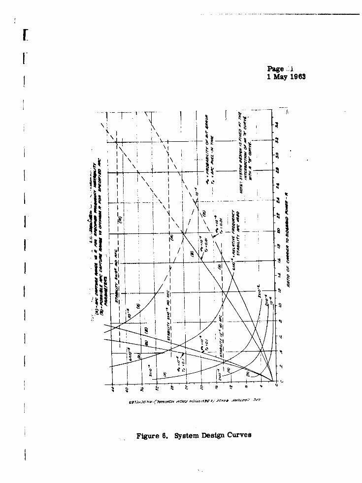
r
I-1 May 1963
N1
14
i tFigu e I6 i Sy te D s g C r 'a
I ~K
'a II
.I
I I
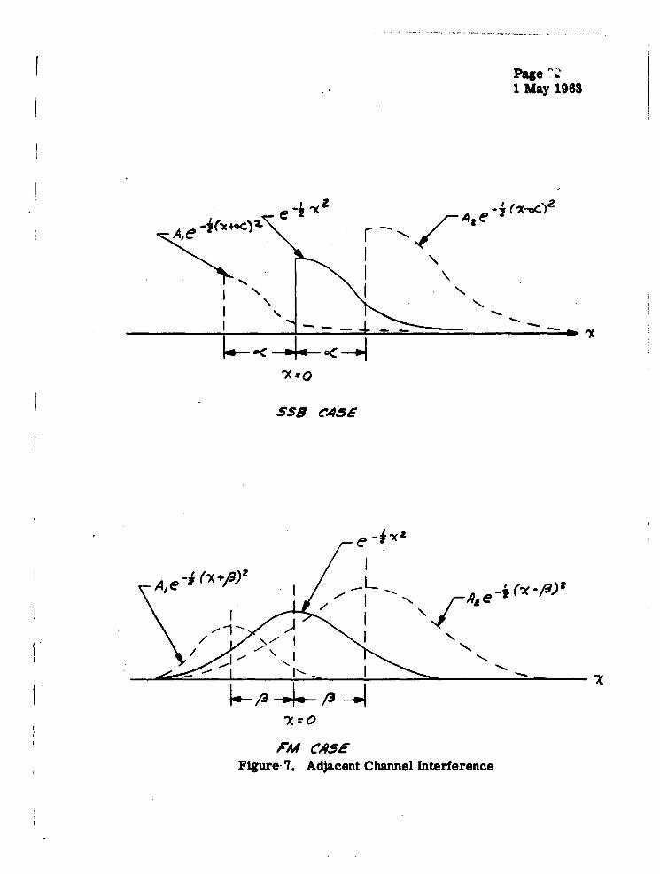
I May 1963
Al -- I
A~e -•('X ÷~ z .. L..
~X:Q
AleZ
-I-/g
AAM CASEFigure- 7. Adjacent Channel Interference

[
Page 831 May 1963
I
~ot%
[
r
Figure 8. Block Diagram of Experimental System

Page
1 May 1963
rnrr
[
I[
I
I
L D-2 51n W1 t S W t
iI
I
Figure 9. Weaver's "Third Method of SSB Generation"

Ii"
I-- Page 0C
I 1 May 1963
I
II
I
M O T6: P/iA'5 OP" '•"/N6TWOQA( MINUlS P/-IA5E
OP" "• "A/FTYVOPX" I/5I~pPOXIMAIELY 90°
1AT ALL MOPU/DrlOM FqILEQMECIE5
Figure 10. Phase Shift Method of SSB Generation

Page,1 May 1963
I
Ii
[
Figure 11. Delay Line Phase Shifter

Page 711 May 1963
41I SSS SI/PAM/.
A/aorc: - - -r,) /S oe1Vo ~e*4(j)BY 65H/,rTWO~c
OF 0- (t&-r) 8Y 9001 WW/LC 0I4/A1.Tiq/A1/AJG~,qppe ox/41 cL>' consrw-AIr ,9mpu ruV(
Figure 12. SSB -"enemation Using a Delay Line Phase Shifter

[I Page 88
I May 1963
,AJ/7TH ORDCR CA ER P/L. T7R."50" REFLECT/ON FACTORp mODULUS C-,.86?
L 2 L4 /6 Le
- rRTIA,41SFER FUMAcT/OM
• S• S /A/ AdC_•A/ADIAIS•
IA diA
-! i• ,.SCg CHEMATIC ATT(rAUAT/OAJ
30.5 fA
Subscript C F) L H) a b
0 - - 2. 0037430 1.0000 -1 .2879 - 1.0218095 1.7117936 x 10"2 .1152 .1125 3.2875877 x 10" 1 8. 559070 x 10 4-23 .2120 - 1.442900 x 10"-1 1.0790901 x 10"-4 1.168 .02125 1. 7648794 x 10"- 2.6977622 x 10"35 .05943 - 4.7367025 x 10⁴- 2. 2143592 x 10"5
2.376 .0106 3.9156594 x 10⁴ 3..69068328 x 107 .1074 - 8.6098532 x 10" 1. 4662904 x 10"8 .5286 .0428 3.1128288 x 10"7 1. 83286314x 10"
9 .1614 - 5.8081886 x 10"
Figure 13. SSB Low-Pass Filter Design

Page 89I May 1963
0- 7,WAW
Fiur 14 CacltdRsos oqS o asFle
II
I I
t 00- 95 '07 ANO.LM SN/
Figure 14. Calculated Response For SSB Low Pass Filter

Page' W1 Ma; . 83
/0 3(T/OMS
ea <R
£2
I.
Section L1 L2 C1 C2
1 24.48 2,875 5,750 24.53
2 8.16 7,582 15,160 8.162
3 5.684 10,958 21,916 4.965
4. 16.39 2,981 5,962 16.42
5 3.564 12,290 24, 580 3.564
6 15.54 2,535 5, 070 15.56
7 4.576 7,853 15,710 4.576
8 4.270 7,626 15, 250 4.271
9. 12.56 2,397 4, 794 12.57
10
AMOT•: /NOUCTOJR VA1 UES ARE IN MICRO-IENRIES.
CAPACITOR VALUES ARE 11V PICOFARAD-S.
Figure 15. SSB Equalizer Design

F
Page -11 May 1963
Figure- 1. C
Fiue16 acuae RsoseFrEqaie

Page S"1 May 1963
gD'bjOv~ - avowd
| A
1 .4 I
IsI'
Figure 17. Calculated Phase Characteristics of Filter and Equalizer -Departure From Linear Phase
I• ÷1

rt Page"
I May 1963
II
\ r/
r N
/\
Fm4M
Figre18 Cmpnet av.'.-m i aPC-SB ig

I ~~Page ••
[ . My 96
Ii
,' '
I (%j " '''
I+ Fiue'.PaeDvatinFoJieryIcesn hs o .
SS-C iayTan 1PleSml
!I

I
Ne Page '
N, "t -1 May 1963
|lz
I -I -I
Ir
Figure 20. Carrier Power Required For the Centroid Frequencyl to be a Given Fraction of the Bit Rate, as . Functionof Gaussian Bandwidth
I

[ Page 981 M y 1963
k _%
I,]
FIA
I -j
----I-
Tr4J
Figure ~ ~ ~ ~ ~ ~ ~ ~ ' 21 F rqenyErrAt adit

FZ
I- Page9 71 h 1 1963
l" i. q xII •
\ .II-4I I
Figre 22.- Frequency Stbility of ,,5B 'Tra~nsmitter Required For a.Specified AFC• Frequency E.rror
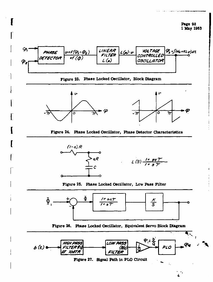
I Page 98
1 May 1963f
Sr/T MR CON rRMoa 00
Figure 23. Phase Locked Oscillator, Block Diagram
0-7 7-
II Figure 24. Phase Locked Oscillator, Phase Detector Characteristics
QR L(S) /4( s)
Figure 25. Phase Locked Oscillator, Low Pass Filter
Figure 26. Phase Locked Oscillator, Equivalent Servo Block Diagram
LOIVP440
Firr x er l 27. Sigeal Pt PRLO CircuitFigure 27. Signal Path in PLO Circuit

F
Page G;1 May 1963
404J $0.\
(r8w)
/A(C
Figure 28. APC Capture Range as a Function of the Parameter

Page 1001 May 1963
APPENDIX A
MATHEMATICAL METHODS AND NOTATION
A. I FOURIER TRANSFORMS AND FREQUENCY TRANSLATION
In this report the principle mathematical tools are based on Fouriertransforms methods. The Fourier transform is defined as:
F~c f(w)C e' w= av*
-Q0
In conventional circuit analysis the symbol, f, is reserved for the real fre-
quency of a sinusoid. Although we maintain this convention, in some discus-sions the term frequency is also used to refer to angular rate, w. Frequently
we are concerned with the transform of the function fCos) &co J, ,o.+l •."This is readily found by using the substitution:
Thus: ( -
T
(A.l1)

Page 1011 May 1963
If the signal zk*•)e4 is filtered by a filter having a transfer function
°Woz), the spectrum of the result is simply equation (A. 1) multiplied by
RCow). When 9(4o) is a high-pass or low-pass filter having a cutoff fre-
quency near fo the result is an essentially single sideband signal. When
this signal is multiplied, at the receiver by 2c4 %c(.4._,P)the result, by
application of equation (A. 1), is:
= e~~~~~~ R-)N-eo.1j +e(L)Ho
Equation (A. 2) is the mathematical result of coherent detection of an SSB
signal. In practice F (ezc4re.)is negligible except for frequencies near
2 epo , and is filtered out by the equipment used to amplify and processthe detected signal. For these reasons the second term in equation (A. 2)
may be ignored. The spectrum of the signal which is received by coherent
detection is, consequently:

Page 1021 May 1963
A. 2 THE SSB SIGNAL
It was shown in paragraph A. 1, that a modulating signal, f(t), after
multiplication by a carrier, 2,,, W,-( , has a spectrum:
If this signal is passed through an ideal low-pass filter with cutoff frequency
at 4 , the result is an SSB signal. The waveform of this SSB signal is
calculated as:
After a simple change of variable and substitution of c- Ces;4 + %,)
one obtains: cos (=-{)
S(A. 5)
The coefficient of cos t is identical with f(t), if f(t) is bandlimited to
twice the first conversion frequency. In practice this will always be the case.
The coefficient of Sih 46 is the Fourier transform of the spectrum
of f(t) modified by a factor -j for positive e) , and +j for negative 40. This
modification of the spectrum of f(t) is identical to a 900 phase lag for all fre-
quencies, and can be used to define the Hilbert transform relation. The re-
suiting time function will be referred to as the quadrature function at). Thus
equation (A, 5) is written more simply:
r(~ r Cos O#-Lsi'n '46 (A. 6)

Page 1031 May 1963
The equation can be expanded to a more useful explicit form by using the
substitution: ) • o
The parameter, , is simply the difference in phase between the trans-
mitted and locally generated carrier, and ordinarily is the error in phase
detection. Equation (A. 3) can then be written:
Fe Cose-5~~c)7 A7
This is a fundamental equation which describes the spectrum of the signal
which is received after double sideband suppressed carrier modulation,
sideband filtering, and coherent reception by a local carrier having phase
error, 9. The equation applies equally well to DSB, SSB, VSB trans-
mission. To obtain the time waveform of the received signal Fourier trans-
form the coefficients of cos • , and sin Pwhich are constants. Thus, the
received waveform is:
_40 (A. 8)
A. 3 THE AVERAGE POWER SPECTRUM OF A RANDOM PULSE TRAIN
In this report we are generally considering a full baud NRZ pulse train
after gaussian filtering. The voltage density spectrum for a single full baud
pulse of unit amplitude is obtained as follows:
T .,i.eT/2z. (A. 9)

Page 1041 May 1963
Note that F(.)) is zero for .) T/Z. =.*7r,4 2,--. Thus, at frequencies
which are multiples of the pulse rate there is no energy, and this result is
true after any subsequent linear filtering.
A pulse train can be expressed mathematically by:
#7a -00
For a binary train, the coefficientso( , can have either of the values + 1 or
- 1. When these values are selected at random, and each selection is inde-
pendent of all others, the train is referred to as a random, binary train.
Usually it is assumed that the probability of o04 being + 1 is 1/2 so that the
train has a zero average value, i.e., is unbiased.
For any particular finite pulse train the spectrum of f(t) may be ex-
tremely complicated. For may purposes, however, the average power spec-
trum of f(t) is sufficient, and it has a relatively simple form. In general,
average power spectrum is defined as the Fourier transform of the auto-
correlation function: Air
hi -%V- r7It can be shown (Ref. 3, page 221) that the average power spectrum of an
unbiased random pulse train is:
where: F(&O) is the Fourier energy spectrum of f(t)
T is the pulse interval (A. 11)
A is a constant equal to the mean squaredvalue of oA( r in equation (A. 10).

FPage 1051 May 1963
For a binary train, ., =:1. When the selection of polarities of o( m is
biased, in general there is also a set of discrete frequency components in
the average power spectrum. For pulse shapes, where the spectrum vanishes
at multiples of the pulse rate, however, no discrete components are present,
even for a biased train. As previously stated,this is true for any filtered full
baud pulse. Note that equation (A. 11) is the two-sided power spectrum,
whereas Middleton uses the one-sided form and therefore an additional
factor 2.
The utility of equation (A. 11) is based on Parseval's formula (see
Ref. 10, page 27)
(A.-12
In words, the energy of a time waveform is equal to the integral of the ab-
solute - squared value of its Fourier transform. For deterministic wave-
forms, f(t), if the waveform is filtered, in a filter having a transfer func-
tion H(QO), the energy out of the filter is given by:
(wE7 U (A. 13)
-00
Similarly, for probabilistic waveforms, such as random pulse trains, the
average power after filtering is calculated as:
P=f S(O (A. 14)
where: ((Q'•o) 'is the average power spectrum
given by equation (A. 11)

Page 1061 May 1963
APPENDIX B
PULSE SHAPES AND SPECTRA
Particular mathematical results, pertaining to pulses and their spec-
tra used in this report, are collected in this appendix.
B. 1 GAUSSIAN PULSE
Assume that the basic PCM pulse shape is formed by gaussian filtering
of a rectangular full baud pulse. The resulting pulse, as a time function, is
found as follows:
A gaussian filter has a transfer function:
e0) e -At I (B. 1)
and a corresponding impulse response:
C4 L ýeW6Ta(B. 2)
-eA
The step response is the integral of the impulse response, thus:
S _ (B.3)
From the step response, the response to a full baud pulse centered at
t = 0 is obtained as:
([4-4(B. 4

rPage 1071 May 1963
The function is plotted in Figure B. 1 for a value of the parameter,
,corresponding to a typical pulse shape at the receiver. Thus, in the
AN/GRC-50 radio (FM) set this parameter would be as follows:
1 1.736 x 10⁻⁶secondsT = 576, 000 bits/sec
= 2.325 x 10⁶ radians/sec for the transmitter filter
= 1.642 x 10⁶ radians/sec for combined transmitter and
receiver filter
= 2.018 at the transmitter
= 1. 425 at the receiver
B. 2 PULSE ENERGY
From the pulse shape, equation (B. 4), pulse energy can be obtained as
the integral of ft6.) over all time. In discussion the term energy is used for
convenience although usually no physical units are explicitly used. This
usage, besides being convenient, is correct if the time functions describing
pulse shapes are regarded as voltages across a resistance of one ohm. In-IJA
stead of integrating xx) to obtain pulse energy, it is simplier to use
Parseval's formula, equation (A. 12). The voltage spectrum of a rectangular
pulse is defined by equation (A. 9), and filter response by equation (B. 1).
Thus, pulse energy, E. is:
E -2f LaT2 ct, (B. 5)

rPage 1081 May 1963
This integral is not a standard tabulated result, but can be evaluated In a
number of ways. The simplest method is to differentiate with respect to
a = 1,4W, integrate with respect to W and again, with respect to a. A dif-
ferent method of evaluation based more directly on physical concepts will be
shown in the following paragraphs.
Integral (B. 5) can be regarded as a Fourier transform of a spectrum,
evaluated at the particular point t = 0. The spectrum involved is that of a
triangular pulse after gaussian filtering. However, because a triangular
pulse is the integral of three step functions, it is necessary only to integrate
equation (B. 3) and apply the result to the required three step functions to
evaluate at t = 0.
A triangular pulse beginning at t = - T, rising to unity at t = 0, and then
following to zero at t = T, has the required spectrum:
T A csj r / .vL (B. 6)
The derivative of this pulse consists of a unit step at t = - T, two negative
unit steps at t = 0, and positive unit step at t = T. In the integral, it is con-
venient to substitute: u'4 4 - 4 so that the gaussian function has the form
specified by equation (B. 1). Adhering to the procedure described in the
preceding paragraph, and using equation (B. 3):
zf (rZ (46w) + [4-k (B. 7)
The integral of function ' is readily evaluated as follows:
I -- fl 00 -L c%, -- C(B. 8)
and,<to'') ' j-'-v- Mir• -•• - e_•: (B.,9)

I
Page 1091 May 1963
Thus:ic-)t (B. 10)
When evaluated over definite limits -0c to y:
Also, ° _ _ _
Applying equations (B. 12) to (B. 7), we have:
~~~~7 (B.,4~~y 13)T~Iz
After rearranging, replacing 4) by , and setting 4:e6 .L we have:
(B. 14)
where: -0..eL, e CLeT/L.
Pulse energy is easily calculated from equation (B. 14) using standard
tables. For the typical constants specified in paragraph B. 1, the pulse
energy relative to the bit interval is given in Table B. 1.
TABLE B. 1
PULSE ENERGY RELATIVE TO BIT INTERVAL
At Transmitter 2.018 0.72
At Receiver 1.425 0.612

rPage 110
1 May 1963
Observe that the quantity E/T is equal to the ratio of power available
when a gaussian filter is used, to power available if no gaussian filter were
used. A plot of this function is shown in Figure B. 2.
B. 3 QUADRATURE PULSE
As shown in paragraph A. 2 of Appendex A, an SSB signal consists of a
modulating signal and a derived quadrature signal which separately modulate
two carriers in quadrature. In this paragraph, the quadrature pulse corre-
sponding to a guassian pulse is derived. Consider a gaussian pulse defined
by quation (B. 2) with a spectrum defined by equation (B. 1). Subsequent to
applying a 900 phase shift to the spectrum, the quadrature pulse is obtained
from:
Completing the squares in the exponents:
e-L3e 3i? dýcj- e~~ (B.l16)
where: 6
Changing the variable of integration as follows:
• '1• v-• -•C oo • (B. 17)
In the first integral, substitute z = - y, and interchange the limits, to bbtaln:6j e. 0 (B. 18)
-Y -L

U
Page 1111 May 1963
Thl result is somewhat complicated but numerical values can be obtained
from published tabulations. The integral is known as Dawson's integral,and tables have been published in "The Journal of the Franklin Institute",Vol. 237, June 1944, pg. 495-497; and Vol. 238, Sept. 1944, pages 220-222.
(See also Jahnke and Emde "Tables of Functions", Dover.)The function defined by equation (B. 18) is the quadrature pulse cor-
responding to a gaussian pulse. For the full baud rectangular pulse aftergaussian filtering, the corresponding quadrature pulse is the integral of equa-
tion (B. 18). To establish this result note that any linear operation, such as
differentiation or integration, has a corresponding operation on the spectrum.The operation on the spectrum is identical for the original pulse and for thequadrature pulse. Thus, if a pulse is integrated, the corresponding quadra-
ture pulse is the integral of the original quadrature pulse. The quadrature
step response is:
(B. 19)
and the response to a full baud rectangular pulse is therefore:
By a change of variable: V= . there results:
,2 (B. 21)7r e
In this form, q(t) can be calculated from values of the function:
_ Z. "(B. 22)
f 1

Page 112
1 May 1963
which is tabulated by J. B. Rosser: in Theory and Application of "aiX
andFl.-P'Y'•:::Jg -y-W , Mapleton House, Brooklyn, N.Y.e, 1948, pages
174-191. A plot of this function is shown in Figure B. 1 for a value of "r=
2.85, corresponding to the case of gaussian filtering at both transmitter and
receiver.
B. 4 EVALUATION OF A DEFINITE INTEGRAL
In Section VI, use is made of the following integral:
Although this can be evalfated as a formal mathematical problem, it can be
derived easily using results previously established.
I can be rewritten as:
7- ~t. MI..
and then noted that I(b) is identical in form to the expression for the quadra-
ture pulse described in equation (A. 5) when:
In this form, F(y) is the spectruth of a full baud rectangular pulse after
gaussian filtering.
Consequently, I(b) is the quadrature pulse corresponding to this spec-
trum. But, from equations (B. 1), (B. 21), and (A, 9) the result that a pulse
having a spectrum differential:
4CQ (B. 24)T

Page 1131 May 1963
will have a quadrature pulse:
SF <•+) <-,/•., , ,(B.,25)
Thus, it is only necessary to identify variables as follows:(B.26)
I I.
With these changes the given spectrum becomes:
(B. 27)
I.which is 4 PI).e(. Thus, the desired integral, I(b) ist timea (*) with
the substitutions: d A7- (B. 28)
Therefore:
(B.,29)
e t~

Page 1141 May 1963
For the original problem, b = 1, so we have:
S':V',ýt eV I &(B. 30)
The integral is plotted in Figure B. 3. In the plot, which is used in
Section VI, the interpretation which is given to the parameter a is slightly
different than that used in the derivation.
B. 5 POWER IN AN SSB SIGNAL WITH CARRIER
Considering a SSB power spectrum it is convenient to regard it as being
identical to the power spectrum of the baseband modulating signal (except for
a translation in frequency of each half of the spectrum). Thus, given a base-
band power spectrum, I 5(j Ithe corresponding SSB power spectrum is
described by:
Iss \i (B. 31)
1o a) <.c.
With this convention, sideband power is equal to power in the baseband modu-
lating signal. When a carrier, Q Cos 4&, accompanies the sideband the
total signal, using equation (A. 6) is:
The power in this signal is Pc + PS, the carrier plus sideband power, where
P - e L P 12 ^P4:Q7-__

Page 1151 May 1963
The quantity PF is the power associated with f(t), and similarly Pt. Since f
and V have the same power spectrum, they contain equal power, so PS * Pf..
The factor 1/2 in the expression for sideband power accounts for the fact that
f(t) is reduced in amplitude by the factor Cos '4), t, and similarly for• (t).
For the special case of ,• = 0, then Cosd t= 1, Sin .U t = 0, and PS = 1
(P;) + 0 (Pt), as required for the, now, baseband signal.
When considering a specific design problem it is usually desirable to
express carrier power as:
(B.33)
where:. R is a constant.
The sideband power can be written:L T)(B. 34)
This form is convenient for the purpose of normalizing results; the terms
have the following significance: F (w) is the voltage spectrum of an individual
pulse; T is the pulse interval; A2 is the pulse train power prior to baseband
filtering; K ((4, , T) is a function of filter bandwidth and pulse interval, and
is the ratio of power out of the pulse-forming baseband filter to the pulse
train power input. For the typical case considered in this report, the full
baud input pulses have unit amplitude, and a train of such pulses have unit
power, so A2 = 1 = A. As shown above, a unit full baud pulse after gaussian
filtering has an energy described by equation (B. 14). Since pulse energy per
pulse interval is average power, and there is unit power into the gaussian
filter, the function K (C4 , T) is:
K( T.,,T A- cc f&..) (B.35)~' ' T 1-5(-

.Page 1161 May 1963
SWhere: * f 2.1 e
Carrier amplitude Q can now be related to the ratio of carrier to side-
band power, R, as follows.
This equation is used inSection VI. An additional relation which is re-
quired is that between carrier power, and power spectral density in the
vicinity of the carrier. For a full baud rectangular pulse train of amplitude
A, 1 .5CO) I A2 T, as may be seen from equations (A.9) and (A. 11).
Therefore:
R4 (B. 37)

I.
Page 1171 May 1963
NKS
UOr
SN" R
lk ftj-% II Ng
A -..
U
Figure B. 1. Full Baud Gaussian Pulse and Derived Waveformsin an SSB System

Page 1181 May 1963
"LAKI
W
ku
-L .Vy "IO( IV49* JOJ0 ýjA
Figur B.. 2. Power Out of a Gaussian Filter Divided by Power Input From aFull Baud Rectangular Pulse Train, as a Function of Bandwidth

Page 1191 May 1963
LuJ-%-
Figure B. 3. Centroid of a Full Baud Gaussian Power Spectrumas a Function of Bandwidth
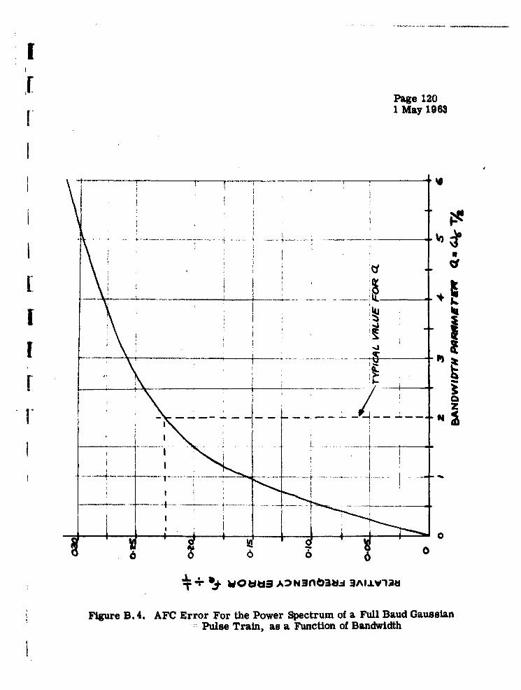
I
Page 120a+ 1 May 1963
'I
t + +
"j I
- I
_ _ .__
-- 0
Figure B. 4. AFC Error For the Power Spectrum of a Full Baud GaussianPulse Train, as a Function of Bandwidth

Page 1211 May 1963
APPENDIX C
AN ESTIMATE OF THE AMOUNT OF SIDEBAND
REJECTION OBTAINABLE FROM PHASE SHIFTER
The spectrum of an SSB signal formed with a tapped delay line phase
shifter is: (Refer to paragraph 3.2. 2)
S(C.l)
Assume that A(4o), the spectrum of the baseband modulation is band limited,
being zero for Ico _ The spectrum of the SSB signal is then zero-roexcept in the range - .\. .. Considering only positive
frequencies, the second term in the expression for S(eo) can be ignored.
The ratio of power in the unwanted sideband to total power can be calculated
as follows:
(C.2)
For the purpose of estimating the number of delay reactions necessary to
achieve a given power ratio, the modulation spectrum can be approximated by:
II

Page 1221 May 1963
Also, note that: I Z< sin W"K-ro1i .~1e when 40>o.
Thus the integrand of the numerator has the form:
C CPO
CPOo
-Sr (C. 4)
+ 'IL- Zo, s,,,AA6+I-,rz)
Because i Is always an odd integer multiple of • then'•;± is an
even multiple of ? , thus, the last two sums consist of terms having
common frequencies and can be combined so that SI( e* g),) can be written:
C*4)
N+i
Now when S1 is squared we obtain many terms of the form:
Upon integration over a half period, or over a full period, such terms
have a zero contribution except when m = n. But m = n only for terms from
the same summation. Thus: O .
-2 O"en +, Y +
]ao ~ (C. 6)-- •t~ N I•'1
Upon substitution of the values of x-y,2+r (,- i )
-, .r ,. _ (ti,--I)( tv-4,) (c.t)

I
Page 1231 may 1963
The second sum can be evaluated exactly with the aid of the formula:
- (C. 8)
which follows directly from formula (222) given by Jolley (Ref. 7). Setting
q = 2, p = 1, and noting that as N--o.' the sum becomes 1/2, we have:
7-__ _ /W (C. 9)N+ I (XI+ /) = zF t ,0)
The first sum can be very accurately approximated with the aid of the
formula used above, as follows:- / fi-Ln) ( -z
r ,2 n .,-7 ) /"0 /____ , ,-,.,, ' (C.11)
Thus: (C .1
#•#'F //N* /
But the last summation has a magnitude less than:
(',.÷ , •" z,'F,-•3(C. 13)
Thus the relative error in the desired sum is less than (2N + 1)-2 which is
less than 1/4 percent even for N = 10.

Page 124I May IM6
The sum:
, ÷4- / (C. 14)
as found by setting p = q = 2 in the general formula used above. As a result,
the numerator of the desired ratio is approximately:
7q1 -- (C. 15)
The denominator of the desired ratio is accurately given by the expression:
-J '-A? (C. 16)
This approximation, is obtained by noting that:
f>C 4)< (C. 17)
and ignoring the small energy contribution from the undesired sideband. Thus:
T.R (C. 18)
SThe desi red i
The desired ratio is therefore:
I~ ~ 5*- -- 42 c 9PUF_ - '0& J %-
-

FPage 1251 May 196S
APPENDIX D
AMPLITUDE DISTRIBUTION OF THE QUADRATURE COMPONENT
AND ENVELOPE OF A PCM-SSB SIGNAL
As shown in the Section V, the bit detection process will be disturbed
by the quadrature voltage when any phase error exists in the demodulating
carrier. In a random pulse train, the quadrature voltage will appear as a
random quantity at the pulse sampling instant. To evaluate average error
rate the statistical distribution of the disturbing quadrature voltage must be
known. Furthermore, the quadrature voltage contributes directly to the
magnitude of the SSB envelope. For these reasons an estimate of the prob-
ability distribution of the quadrature voltage is developed in the following
paragraphs.
D. 1 THE QUADRATURE DISTRIBUTION
A random binary pulse train can be described mathematically as:
60• ) a ,-(*i'lT• (D. 1)
where: e = 1 chosen independently, at random
p(t) is the pulse function
A similar expression describes the quadrature pulse train, b(t), except that
p(t) is replaced by the quadrature pulse, q(t). The particular functions, p,
and q, used here as typical examples of PCM pulses are described in Appendix
B by equations (B. 4) and (B. 2 1) respectively, and are shown in Figure (B. 1).
Now if b(t) is sampled at the bit rate, one obtains a set of random quantities
having some statistical distribution. The mean square value of this distri-
bution is shown to be:
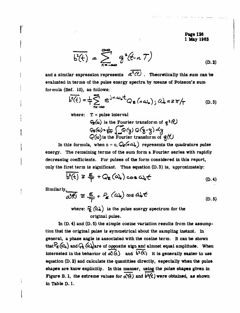
Page 1261 May 1963
(D.2)
and a similar expression represents •-t') Theoretically this sum can be
evaluated in terms of the pulse energy spectra by means of Poisson's sum
formula (Ref. 10), as follows:
Tl -00
where: T = pulse interval
•oc) is the Fourier transform of -
Q(co) is the Fourier transform of
In this formula, when n = o, QI(M '4) represents the quadrature pulse
energy. The remaining terms of the sum form a Fourier series with rapidly
decreasing coefficients. For pulses of the form considered in this report,only the first term is significant. Thus equation (D. 3) is, approximately:
1- +L +Qj)c-o s~ (D. 4)
Similarly""T" r( ) o (D. 5)
where: PE (L%) is the pulse energy spectrum for the
original pulse.In (D. 4) and (D. 5) the simple cosine variation results from the assump-
tion that the original pulse is symmetrical about the sampling instant. Ingeneral, a phase angle is associated with the cosine term, It can be shown
thatPE ) andgC (&k are of opposite sign and almost equal amplitude. When
interested in the behavior of at) and U it is generally easier to useequation (D. 2) and calculate the quantities directly, especially when the pulse
shapes are know explicitly. In this manner, using the pulse shapes given inFigure B. 1, the extreme values for a.n) and ý1 )were obtained, as shown
in Table D. 1.

Page 127
r 1 May 1963
TABLE D. 1
Sampling Instant
Quantity Pulse Center Pulse Edge
0.8526 0.7043S0.6892 0.8631
_ _E_ 1.09 0.90
f 5- W&)' ý/ F 0.882 0.11
[ \-= Rms value of a(t) and b(t) = 0. 781
1:o) = Peak Pulse Amplitude = 0.846
From the table it may be observed that in general the distribution of
a(t) and b(t) must depend on the particular sampling instant chosen within the
pulse interval. Although a(t) and b(t) have the same average rms value over
all possible sampling instants, for a particular instant (e. g., the desired
case of sampling at pulse center), a and b have different rms values.
To determine bit error probability, the distribution of the quadrature
voltage at pulse centers is the only consideration. In principle, this distri-
bution can be determined from the expression:
•6 (o) cT( s n w" , at random, (D. 6)
A: -00
for any particular quadrature pulse shape. It is actually impractical to carry
out this procedure due to the very large number of terms which are required
to adequately approximate the sum. Instead, advantage can be taken of an
interesting property of quadrature pulses i.e., for any practical pulse shape,
p(t), which is narrowly confined in time, the corresponding quadrature pulse
rapidly approaches the asymptotic form K/t, where K is a constant. The

[Page 128
[ 1 May 1963
asymptotic form is shown graphically on Figure B. 1 where it may be seen
that for times greater than 1.5 pulse-intervals, the approximation is excel-
lent. Also, for symmetrical pulses, the quadrature pulse is zero at pulse
center. Thus equation (D. 6) is approximately:
- -(D. 7)
The distribution described by this equation can be obtained, at least numer-
ically, and this basic distribution can be used with a correction process to
obtain the distribution fGr any particular quadrature pulse. A correction
process of this type has not been applied for it is believed that the basic
j distribution is sufficiently close to the desired distribution. The process
for obtaining the distribution of bo as described by equation (D. 7) is out-
lined below,
First, consider the variable, x, defined by:
(D..8)
Since x is the sum of independent random variables, the characteristic
function for the distribution of x is the product of the individual characteris-
tic functions. The characteristic function for the nth component is:
Thus, the characteristic function for x is:
(D 0

IIPage 129[ 1 May 1963
It has been shown by J. Dutka that this infinite product can be expressed as:
(D. 11)
In this form the characteristic function is recognized as that which results
from an infinite sum of random variables, each having a rectangular distri-
bution of different widths. A close approximation to the distribution of x can
be obtained by considering the sum of a limited number of these rectangularly
distributed variables.
Mathematically, a repeated convolution of the rectangular distribution
must be performed. Further accuracy is obtainea by assuming a normal
distribution for those terms which were ignored. Using some results of
SJ. Dutka (see acknowledgements) which give explicit formuias for the results
of convolving rectangular distributions, M. Landis obtained a very good
1approximation to the distribution of x. The excellence of the approximation
obtained by hand calculation was confirmed by a computer calculation which
was programmed by M. S. Corrington and T. C. Hilinsky. The computer
program involved a calculation of the distribution function J9*(1" in the
form of equation (D. 11). The first 1000 terms of the product were used.
A Fourier transform program was then used to compute f1 (x), the prob-
ability density function for x.
Having computed the distribution of x, the distribution of the sum of
two such variables can be computed by direct convolution, or, by squaring
the characteristic function 9 (') and Fourier transforming. The results
of the calculations described above are shown in Table D. 2. In this table
are given the probability density and distribution functions for x and y,
where x and y are random variables formed as follows:

FPage 1301 May 1963
x +'•4 , 1, - 1 each with prob-
ability 1/2, with random inde- (D. 12)y =pendent choices.
The variance and standard deviation of these distributions are:
S= 1. 64493 . 1.28256"L ~(D. 13)
= 3.28986 0- 1.81382
The probability density function for the normalized variable '4 1o/%is plotted in Figure D. 1. Normal distribution having the same variance is
also shown for comparison.
The normalized distribution described is the required distribution ofbo as given by equation (D. 7). The constant K need not be explicitly eval-
uated, but is chosen to insure that bo has the desired rms value. The rms
value of the quadrature voltage was made equal to the nominal pulse amli-
tude ao was chosen somewhat arbitrarily for the purpose of calculating error
probabilities. This is a pessimistic assumption, for as seen from Table
D. 1, the rms value of bo at pulse centers is actually about 19 percent less
than the nominal pulse amplitude, ao. On the other hand, the approximate
distribution defined by equation D. 7 gives a result more optimistic than the
exact distribution defined by equation D. 6. In addition, intersymbol inter-ference has been neglected.

Page 1311 May 1963
TABLE D. 2
PROBABILITY DENSITY AND DISTRIBUTION
FUNCTIONS FOR x AND y
x, y fl(x) Fl(x) f2(y) F2(Y)
0 0.25000 0.50000 0.21035 0.500000.1 0.24999 0.52500 0.21004 0.521020.2 0.24997 0.55000 0.20912 0.541990.3 0.24992 0.57499 0.20760 0.562830. 4 0. 24980 0. 59908 0. 20550 0. 58349
0.5 0.24955 0.62495 0.20285 0.603910.6 0.24907 0.64988 6. 19969 0.624040.7 0.24821 0.67475 0. 19606 0.643830.8 0.24678 0.69951 0.19200 0.663240.9 0. 24453 0. 72408 0. 18755 0.68222
1.0 0.24122 0.74838 0. 18277 0.700741.1 0.23659 0.77228 0. 17769 0.718761.2 0.23041 0.79564 0. 17236 0.736271.3 0.22253 0.81830 0. 16683 0.753231.4 0.21285 0.84009 0. 16113 0.76963
1.5 0.20142 0.86082 0. 15529 0.785451.6 0. 18835 O.88032 0. 14934 0.800681.7 0.17385 0.89844 0.14331 0.815311.8 0. 15823 0.91505 0. 13723 0.829341.9 0. 14181 0.93006 0. 13110 0.84276
2.0 0. 12500 0.94340 0.12494 0.855562.1 0. 10819 0.95506 0. 11877 0.867752.2 0.09177 0.96505 0. 11260 0.879312.3 0.07615 0.97344 0. 10645 0.890272.4 0.06165 0.98032 0. 10032 0.90061
2.5 0.04858 0.98582 0.09422 0. 910332.6 0.03715 0.99009 0.08818 0.919452.7 0.02748 0.99331 0.08221 0.927972.8 0.01959 0.99564 0.07632 0.935902.9 0.01341 0.99728 0.07053 0.94324

Page 1321 May 1963
TABLE D. 2 (Continued)
x, y fi(x) Fl(x) f2 (y) F2 (y)
3.0 0.00878 0.99838 0.06487 0.950013.1 0.00547 0.99908 0.05935 0.956223.2 0.00322 0.99951 0.05400 0.961883.3 0.00179 0.99975 0.04885 0.967023.4 0.00093 0.99988 0.04390 0.971663.5 0.00045 0.99995 0.03920 0.975813.6 0.00020 0.99998 0.03475 0.979513.7 0.00008 0.99999 0.03058 0.982773.8 0.00003 1.00000 0.02669 0.985633.9 0.00001 1.00000 0.02311 0.988124.0 0.00000 1.00000 0.01983 0.990264.1 0.01686 0.992104.2 0.01419 0.993654.3 0.01183 0.994944.4 0.00975 0.996024.5 0.00795 0.996904.6 0.00640 0.997624.7 0.00510 0.998194.8 0.00400 0.998644.9 0.00310 0.999005.0 0.00237 0.999275.1 0.00178 0.999485.2 0.00132 0.999635.3 0.00096 0.999745.4 0.00069 0.999835.5 0.00048 0.999885.6 0.00033 0.999925.7 0.00022 0.999955.8 0.00015 0.999975.9 0.00010 0.999986.0 0.00006 0.999996.1 0.00004 0.999996.2 0.00002 1.000006.3 0.00001 1.000006.4 0.00001 1.000006.5 0.00000 1.00000

!Page 133
1 1 May 1963
D. 2 THE ENVELOPE DISTRIBUTION
Having obtained the quadrature distribution, as previously described,
an approximation to the envelope distribution is obtained as follows. The
envelope e(t), is defined as:
j Because a(t) and b(t) are Hilbert pairs, they are uncorrelated variables, butnot necessarily statistically independent. When the pulse train has negligible
I intersymbol interference, however, ao and bo (the values at pulse center) areessentially independent. Also, under this condition, ao is a constant. Thus
I the normalized envelope is:
66Z"/0,6 (D. 15)
C0L0
I" The probability that the normalized envelope exceeds some value, z, is:
a (D. 16)
Using this relation and the distribution obtained for bo/ao, the probability
that the normalized envelope at a pulse center exceeds a given level is ob-
tained. This is given in Table D. 3,.
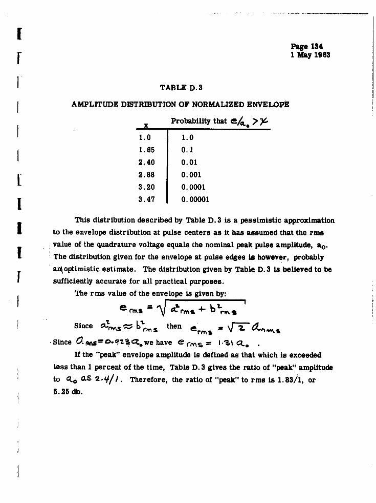
!Page 134r" 1 May 1963
I TABLE D. 3
AMPLITUDE DISTRIBUTION OF NORMALIZED ENVELOPE
x Probability that e/ )
S1.0 1.0
1.65 0.1
2.40 0.01
[2.88 0.001
3.20 0.0001
3.47 0.00001
This distribution described by Table D. 3 is a pessimistic approximationi to the envelope distribution at pulse centers as it has assumed that the rms
value of the quadrature voltage equals the nominal peak pulse amplitude, ao.
I The distribution given for the envelope at pulse edges is however, probably
anA optimistic estimate. The distribution given by Table D. 3 is believed to be
1 sufficiently accurate for all practical purposes.
The rms value of the envelope is given by:
OAS iiarr~z -4- 6Lr,%,Since o 6 then
Since Cmso =o- . we have eI tS I.c C,If the "peak" envelope amplitude is defined as that which is exceeded
less than 1 percent of the time, Table D. 3 gives the ratio of "peak" amplitude
to 0.0 O.S 2 a,/I. Therefore, the ratio of "peak" to rms is 1.83/1, or
5.25 db.
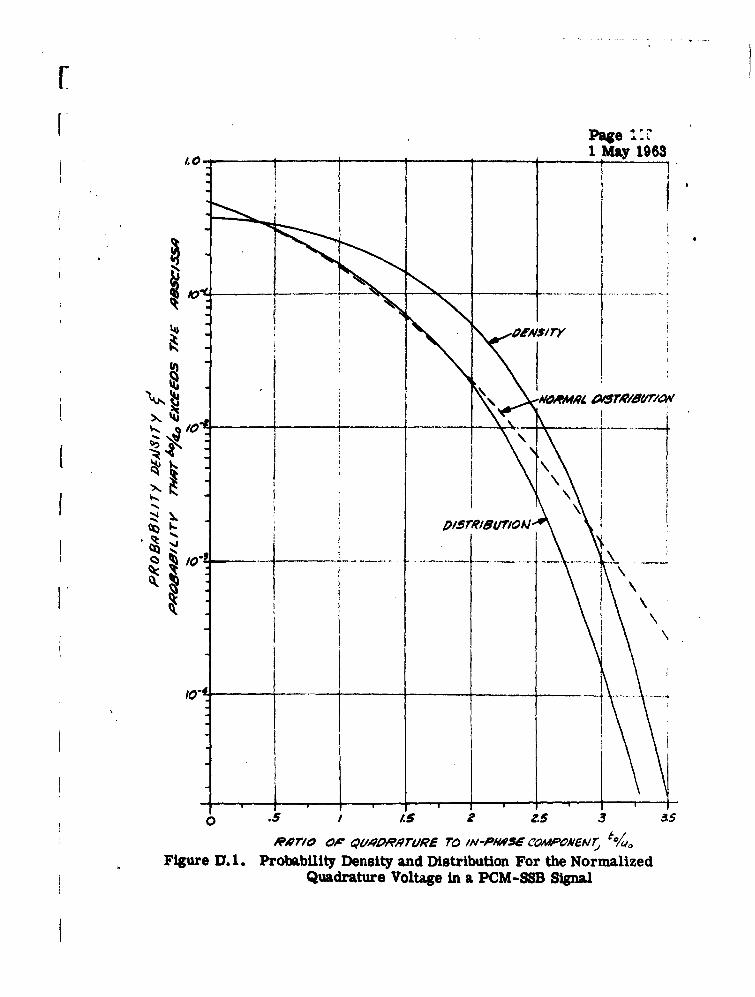
[
Page ::40_ 1-_ May 1963
I v
*, o,& oaq TRe ra IN-pM4 -w coMPOAiN,7Figure U. 1. Probability Density and Distribution For the Normalized
Quadrature Voltage in a PCM-SSB Signal

Page 1361 May 1063
I APPENDIX E
I THE ELEMENTS OF A FREQUENCY LOCATING SYSTEM
This appendix considers the operation of limiters, discriminators, anddetectoril,and their use in an AFC system for SSB signals. These devices
[ are usually part of an FM demodulator and due to the wealth of experiencewhich has accumulated for FM reception, can be taken for granted in that
[ application. When the devices are. used to process SSB signals, which have com-pletely asymmetric spectra, it is worth reexamining the behavior of at least
the idealized models of these devices.
E, 1 LIMITERS
SAn "ideal" limiter is a device with an output of + 1 when the inputsignal is positive and - 1 when the input signal is negative. Thus, after
[ limiting, only the location of zero crossings is preserved in the output.
From the usual representation of a narrow band signal:
6 (E.1)
it is clear that zero crossings are determined solely by the total phase:Q -4f-0- f (•) Also, all signals having the same phase functionwill become identical after ideal limiting. The question now arises as to the
extent it 6 possible to convert the signal, s(t), to a purely phase modulated
signal of the form: CoS("r4if -0. i). That is, to what extent can anideal limiter be said to remove amplitude modulation and leave phase modu-
lation unchanged? This question is answered as follows:

IE
Page 1371* 1 May 1963
The limiter output is a function of Q, such that:
- i) < < (4.A-s) ( 2)•lli_:'.tl i23 !...
Cos (E. 3)
where: S= _-(-I .
The last relation is simply the Fourier series representation of the square[ wave, P(Q). Except for a change in magnitude the first term in the summa-
tion is:
I The desired pure phase modulation. The remaining terms are pure phasemodulations of multiples of the original carrier frequency. If the spectrum
Ii of the first term does not overlap the harmonic spectra, a simple filtering
operation is sufficient to remove all but the desired pure phase modulation
from the limiter output. In answer to the question raised, it appears that if
the spectrum of Cos f(e) is essentially band limited, then for a sufficiently
high carrier frequency all amplitude modulation can be removed with an ideal
limiter and low-pass filter.
E. 2 DISCRIMINATOR
An ideal discriminator is a device whose output voltage is proportionalto the instantaneous frequency of any input signal having a constant envelope.
Given an input signal, it is easily shown that by differentiation, and envelope

I
Pa.s3 81 May 196
detection, the required property of a discriminator can be obtained. Thus
(E.5)
and for I (c4 , the envelope of the derivative Is just:
(E. 6)
The requirement that the envelope be constant is important because if:
SJ eV cc (,K)) (E. 7)
then = R os('4a jo0 'at44ý Vtv
The envelope of this signal is:
1~~~~~~ 4ý LRýT94-, f- C 4' ) (E..8)
This signal is clearly very diffprent from the usually desired output, d4-#
unless R is constant.
From well known properties of Fourier transforms, a differentiation in
time is equivalent to multiplying the signal spectrum by j4i. Thus, the re-
quired operation is filtering,utiliing a filter whose amplitude response is
proportional to frequency, with a 900 phase shift, over the band of significant
frequency componeits. For proper discriminator operation the requirement
of a 90* phase shift is unimportant, since this only has significant effect on
the carrier, and is removed by subsequent envelope detection. Practical
discriminators also make use of a balanced circuit for removal of the constant

APage 139I May 1983
term corresponding to the carrier frequency. The basic circuit element of
an ideal discriminator is therefore, a filter having a transfer function which
varies linearly with frequency over the band of interest. The band of interest
is the band containing significant frequency components of the phase modulated
carrier, and may have to be determined experimentally.
E. 3 DETECTORS
For the purposes of the appendix an ideal envelope detector is a device
with an output voltage that is a function of the "instantaneous" envelope of the
input signal. Practical devices can be regarded as having a linear, or a
square law relationship between input and output. It must be assumed that
many carrier cycles are completed before the envelope changes significantly.
A square law envelope detector can be represented mathematically as a
squaring device followed by a low-pass filter. Thus for an input signal with
envelope and phase variations, after squaring:L= RZt cos,' ('C,6 0 -4
C=-(_. (E. 9)
Assuming that the spectrum of R2 does not overlap that of cos
after low-pass filtering only the term 1/2 R2 will remain. The squaring
operation generally consists of full wave rectification utilizing diodes, and
using only a very small input signal in order to take advantage of the large
curvature in diode characteristics near zero input. For a linear envelope
detector, the same circuit can be used, but with a large signal input. Applica-
tions involving AFC circuits generally concern the mean detector output. For
linear envelope detection the mean output is the mean envelope. For square
law detection, the mean output has a simple interpretation in the frequency
domain because of Parseval's formula (equation A. 12). Thus:

[PWg 140
Q1 Iky 16$
where: I ) (a)) j - is the power spectrum of R(t)
E. 4 FREQUENCY LOCATION
Using a discriminator with or without limiting, and thjn either squarelaw or linear eshvelope detection, four basic devices for frequency locationare obtained. Two of these give a measure of location, which is difficult tointerpret theoretically and will not be discussed here, although possibly ex-
periment would show them to have special virtues. The other two combina-
tions are:' Limiter, discriminator, and linear envelope detection; and nolimiter, discriminator, and square law envelope detection. The first com-bination develops an output proportional to the average instantaneous frequency.
The second combination develops an output which can be interpreted as anoperation on the power spectrum 6f the signal. The latter is analyzed as
follows:
For a discriminator assume two filters having transfer functions:Dl(o•), and D2 (0o).
The signal is separately passed through each filter, and each output issquared and low-pass filtered, (i.e., square.4aw envelope detected). Thedifference of these outputs is then "averaged" by a low-pass filter and usedto control the AFC system. The mean value of the difference voltage is cal-culated, by Parseval's formula, as:
-(E.011
where: ISco) jus the signal power spectrum.
I

Page 1411 May 1063
The equation clearly shows that the average voltage-at the discriminator output
corresponds to a weighted average of the signal power spectrum. A great
variety of characteristics can be obtained by varying the characteristics of the
amplitude response of the discriminator filters. Note that phase response is
totally ignored. Because of the great flexibility of the formulation a circuit
designer has an embarassing degree of freedom, for it is not clear what
weighting should be applied to the various frequency components of the power
spectrum. The basic goal is of course, that the discriminator output should
be zero when the signal spectrum has been translated in frequency. This en-
sures that the carrier is within a specified narrow frequency range.
No attempt has been made in this analysis to determine an optimum fre-
Squency weighting function. However, the conventional linear discriminator
response has been studied to gain some insight into the behavior of a typical
system. Assuming the following symmetric linear forms for the filter ampli-
tude responses:
DI C )17. 41 4E.1(C
This result is substituted in equation (E. 11) and the mean discriminator output is:
2.A S(E. 13)
o

Page 142[" I May 1963
The discriminator operation can thus be described as a calculation of the first
moment of signal power spectrum, about the center frequency, Wd, of the
discriminator. In an operating AFC system the signal spectrum is shifted
until eo, hence the first moment, is zero. If the power spectrum is re-
garded as a distribution of mass, then the spectrum is shifted until the cen-
ter of gravity, or centroid coincides with Wd. The centroid frequency is
not generally the same as the carrier frequency; and the difference is the
AFC frequency error. (To the extent that this difference is known and con-
stant, it can, however, be compensated.)
The steady state frequency error can be calculated from equation (E. 13)
as follows. The discriminator output eo ts zero, and the signal spectrum is
shifted until the carrier is located at C), . Let &O.). c4 ( , tl~en:
[ / s(,--6.Z.(• +Oe-• • - C O( (E. 14)
For an upper sideband SSB signal, S ( &) + c+. ) is zero except for a- O>
Transposing terms in this equation, the frequency error is:
,*ere: I•'t)l III"(E. 15)
where: Is (0/1) (is the power spectrum,
referred to baseband.

!Page 1431 May 1963
Note that the denominator is proportional to signal power, and that the ratio
is independent of any multiplying constant associated with the power spectrum.
Also, if the spectrum has a line component at the carrier frequency, thisappears in equation (E. 15) as an impulse at o(.= d , and hence does not
affect the numerator.
[
I
[
i
I
[
I
I
I

Page 144[ 1 May 1963
I Supplamental Report
BIT-ERROR RATE IN SSB-PCM
DEPENDING ON SIGNAL-TO-NOISE RATIO, PHASE JITTER
IN RE-INSERTED CARRIER, AND QUADRATURE DISTORTION
BY
S. Weber
I
t

I- Page 145
OoTX~~t~S1 May 1963
le lutrodaction
2. mathenmt~wl Thriation 3
3c Eciydvaln to Noise of Iiiame Attaor
6~ Del t-d.mtion of Error Rates8
5c Detei'~wnatlcu of rem Phase Jitter, 1
Appiendies
10 Statisticul Maepandowe of Hilbart INobive PAdrs 12'
2. Proof Vat P[-#+c 0S 0 S0 0 ] O:S n 0"]
.4. -Rmftt~ia CE6Y, th) p(w)§(-acosq5+ bsinO)d0 1-75. Proofs of (26)-.(34) 1
6. Proof Of (3.)25
FiMu"S 1-5 28,
Referencea s

Page 146I" 1 May 1963
I.
I
I Abstract:
I An SSB pulsed signal, plus noise, in the IF filter is mixed
(multiplied) with the output of a phase-jittered oscillator. The
I product, after being passed through a low pass filter, is sampled
I at the bit-rate. Error rates at the LP filter output are determined
and curves presented. These include the effect of fixed values of the
I quadrature component.
IF
I
I

"Page 1471 May 1903
f Gontdder Figure 4 hmre no quadrature lo asmumod to be present at tbe
tirs of vilipng. Plotted here ario curves of error-rato versus sigma1l;noe
ratio in the IF, depending on the amount of phase jitter In the injected
aarrier (PLO)o The signal-noiso equivalent of tho phase Jittor on the
injected carrier is also notedo At the time of &nmoling tho desired in-
phase coponeft is either plw one or mimm ow in a binary syate% or to
put it enathsr war the in-paso comonent of carioer in in one of its two
possible pbaseso Phof s errors in the PMO, w.hbch cvct like a phasw reference
in a cothme t detection syteu, thus produce bit-orrore. The eawrorate
eurve farthast to the left is the case vhere no plkwv jitter existtse and
errors arise due only to notese in thoe ignal chantisi The result is the
wef;!•nm error-rate onwvf for coborent FSK detection. About oni d' to
the right is a dashed curve dnoted as '.diffocmtl-al PM"o Intorsectiowm
of the dashed curv with the errorrWs curves deermire points at which
the si l-naomse in tmhe svigl channel equpAl the equivalent signal.nolse
in the reference phase, The error-rate at wtch points are thus given by
the wual4cwAn DPSM formilao Beyond this potn,,. for a givxn phace.jitterp
there ts a sharp drop to a constant error-rate% i.-rspcative of Zwhe
increase in radiated powtere
Mw the amwvoo of Figure 3 shov hft this iyd-ting, constant errvr-
rate is influenced V/ the presence of the curadrature component at the time
of sepliugo It is eown that the quadrature ac*ucuont has no effect until
it cc=ss tdtbu 3S db of the dasired cm•n •ent* in the naxb $ dbD the error-
rate approximately dob1•.e The quadraturc: evel here is one-third the deuired
lovelo For further ifteasea in quedrature lovel, the error-rato rives rapilY,
icreavint; IT a factor of ten, aprroxLtzely, u.ahr, the ratio of quadrature' to
in-phase oee~ownte is one-halfo Figures I and 2 each contain the saw
inforsation as figure 3o

Page 1481May 1983
Consider' tbae followutM ay~t uwd f~or Ifte reooptloau of. tr~zann1ted
nark mi.a mc u,
0 w PaSt
pi sci/4 tor
CAr

I Page 149'1 1 May 1963
The received signal plus noise, and the pilot tonw am fed into
the Ii filter and the phaes-locked oscillator (TW), The filter output
is signal plus noise (the pilot tow haiig beon rejected), and the
oscillator output is the pilot frequency ieth a random phaae parturba-
tion due to the interference at te ilrut to the P1DO Those two ou.
Sputs are passed to a mL-wr (matiplier) and thon integated in a low-
peas (LP) filter, The LP filter output is fed into a gate which sm~pls
I its irmat perloica.aUy The gate output im thon fed into a pulo re'.
generator vhich rmcostoitutes the tranmr*tod bit-streai except for
®rrors in decisiono The pmob3i considerad hore in to dateruine the
I probability of an incorrect decision0
I

Page 1501 May 1963
~IT= let tho sim al t tbe 3F Bi7ter output~ at t1io be defi~id br
MI sit) ~. aft) cosG00t) + () i-ot
vitot*) a 0nd 6 Q-) for iecamso of a Aingle tranaitted mark
qmdau OPMato ditartion g~s by oupprooing ow ifbad
w~ po~alt-lev indkz~*.d f~or tim) fwa or anuppor sd.
ban t-.-ntW~n,*If the Iomer midabarA4 Izm =zomctod om need owly Lnver',
the qurAmtm-9 empeemnts shomm, Famver, oith zT chiolce do)-,z Wct affm.&

Page 1511 May 1963
The idea1 ssm~ping tim So at th,& pcvic of the C1(~ pulse &t
- ehio t± b U i's ,Pr ,a siera (in f eot exn~,tly zero if i
is symetrical)0 Almo =mp~frM iu=,euromLo vM41 e arm~ tDS e ii ths
Idasired peak sLight34. and tau3 evan -if b(+ urar cz-hactly zeoo
at the peak., ons rmmd va-rple vom non-zero vallao of quadrature distort~ion.,
Furthav~oro, the cor~parat4.ve &mounta of dool-red azd quadratuire levela
uamplcd deparA on the eacur.aoy imith uahichi the p~ŽaEo of tba pilot tone
%ms "been m4-d (mailtip~ed) -%Ith the erIl~m chmmmie1 An obviousi mramv
in a phase error of 9oe* uhich romtout I- n =.. plt~ of tha qumdratuwre
compotiont mlv. Tlr. 3SBB pUlse tmr-mi zon hae Inbm-ant Iuolzo" L12
iU doe-tdirg on ths factors- Pointod out abov'o. Theae wre incluided in
j ~tb* aimlysis presenited.
We reprot-ea th3 real noise at, the IF filtcer output b7r
n a) r(t) x ~C'OS(wof~ + .YO) in(W.0~
,*a 'and Y# W~ ame statlstica]Iy ittpendenut gmmvssia
rmAdam variables mdith zeo-- me~ms and unit vz iaoes, inep
weore Porizont'ala bars domte oither tire or eristeble Uverageso ibe 0
S(H a nd y '~~ re assun~d 'to ba =merm of o rgdJc oa~tiozv-

Page 1521 May 1983
* e~#(+) Is a etingla-siiamband oiguul0 Thus x4t) and y(t) oonstitut~e
-a Ilabext frangfoill pair* This functional dependewe of x(t) uand 7'(t)
can be elrets nwt to cntraditof the fact. that x(t) and y(t) an e atist~ically
indepandento
Lst be the phase Sitter of the piviaelocked osaillatoi'ow.hers -Fr4c0: V 7?and is az random varisible whone davaity win be
spealfted-latero.
Nc cnserth uantity ~Swt nmt) cs O*0(z9W )that ise the LP filter input* We have froRm (1) and (2)~
Cs) [~+h mlCos.w ' + 0()M .+ t KMos_4__10 sip
A~)a R-)(t +~)Y t £ivMt
+ ALLA±.cosIcuot + 06((A6()+ -
1¶wze Vt),tim LP filter Output.9 ia SLven by
Then WOt in Vwe eaniov of trai~eritted .martc and vopaos i3
(2) V5() +1 W0Lf~t Cos 6(4) b()+*V)
*Soo Referercev I =d 2o0*
*6See Appeaftz I

Page 153
1 May 1963
zbw if v(-r)>'o (V(T)•),, nuat asmtoa zu
(apace) msi transwitod. Then btao averamge orror E io glon by
(9) E Pm [ V (T) < 01 M PS' Pv(7) > 0S)
Imr P, I w s ae*o a priLor probabil~ities" or.
1mv ovevn probab-1lityj dsnvi1-*, ftnotLoton U"0-fw have
ato 0[V (T)<ObnI [(T) v (S
0 T.2X( T
11o fzmV;M02 sOti

CPage 1541 May 1963
Tat no defing tfia phase j itter 0 oth -icedcarrier to have
the probability deuuAtyv p (i) p~ wj'Ub ansuwe to be the
result of the presen•e of a certain noise added on to the in.serted
carrier uhich -prod.ces a phase Jitter equivalent to that at the output
of a P•*0 The actual jitter distribution has not as yet boon solved
due to dif.iltios in the a•alymii of bho PID * However, at total
signal•-to-ititerferenee ratios of 3 db or wore at th* iputq. the PFMtakes on rnre and more of a linear transfer character. Under thece
conditions the P. output oarrier, thmugh amstantaly consta•t in
aylitucb, will have m pbase variation esaonti•nly as though. a certWai
amsounkt of mis~e vein addod to lanlId outputo This am=%n of tolve Is
referred to in Vhis pro.entamtion P.9 the er"lvalentnoise corresponding
to a given mmi phame Jittaro Figuro 5 of tis report proeides a curve
showitig the correzmondamnae bmtxmen raB pham~ jitter~ arnd the equivalont
riln--ise iu the Lneerted carriar0
The probabiitty dene.ty on phare jitter is thus gi3ay by2. 1 +'ZfP C SO(1q) P(O):. [1+ i w , cosSetc• c0s. .(,•cos•) INkw
0o, k >bfTr
('"> ~() = • f• e zdyAt. ti'trermes w. have
c•.. •, >]•=o [ IcN "
'1
Curea ~rp (0) ame chown on pap.~ 418 reforonce 3, wheare the value
(7}to bp..uvvd In equation (9.58) cmd Blzmro PA~ in 0

Page 155t 1 May 1963petmmiirnttion o.f
wo ot dotcrmivinz t' orr- rat~es in rthnmisolens and noice css
~ ____have
WO L~c, s~ 0 S "'0 <
rac0 r ~ Z-:bS ,, '0
p Ao
(",C)dt~ t7 rhoi-f tho
pamm orzicoveric -ret,-
Ss2to AnowxI~
.wIvc
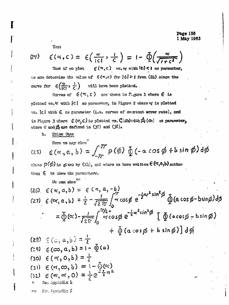
Page 1561May 1963
TWOifVD P~yc E(%c) c v. f)th 1c O 's ywsmazver 1'
ami chtl'o'ta- in-tht talur of (-:,c) for I CI ý> f m~ (24&) sxie the
cm-7afor ( , Ic ) c - -,LL have bceen plottc-d.
aarv of~ c ) av , iotn -.1 P-gure I s-.mrs E t
P:LVeV vact0 With IC I au aa~cn. in Fliawcy 2 vhmzm ? im plaotted
v, Ic I~t To C n pmrmter (±io. curves of coin'ant error rate)~, mAn
in BLmr 3 vmarc C (ct2 C) lo plottsc1 -To C -%db) ithU (db)' as aamegtyanr C andf4ara def-Inad ini (37) and (385.
F.m Tv~ may cl:m
jO(6 is g6v.a by (21s), zmý -nmr -emavo t-mit~elmE (01101b) mathiar
tsE t.- r,'-oi tb- ian~
"fie4 es Tea4m( cs"b~(ai)E(a) - /
(W a o

I- Page 1571 May 1963 '
,I- (34 -- oLim E•(7,a7 a~c = 7I- 0<<-~c O
rofmatO, y It was not po-Sdb to peroru th4 required.
Integration in (25) or (27) to obtain. E(Ca, -) o. ;a.,new, 6)..
caq be 29armd of the ohapo of 6012dfh)ourves fern (28)..(34) ad' 0=* ia~r.ca. Ift•gratious 'for speci.Io yaw.a Of a, and b.o.
- NOv make -the followine definitionse
(35) A (•b)W = 20 to :-
1/ 1~L(36) B (rib) = ao to,
F('1) .20 103'.) 2Ptoo
),b) 2 1 t Ica. B-A7 b
I 0+"]
Figure IL iham 6,(l t,o Co A with as p -rauto "na+dedie the graph of (32)o It Is seen tblt the curyos, for lager values of
a., reach tbw 1iatitng value of %X( imby (31).
From (34) ad (24) It is aeon that Fiuree Is 2s arA 3 in
adr~tion to bIng cuarves repreeentirng (24) ani raw~ curve a MrUMnin (34~).
II

Page 1581 May 1983
We now 'consider the rm~s value of i*C OTwb
1)"O
V p(0) ingi18 b (24). The'moutprac*Aaaawut~ad of
dateminitg 0'APPeared to be MUmIelcal integentlon, 00e reslte of vbicfh
are shoun in Figure 5o .Che intogrations iraer peirfni~d using the result
(L) + er(- sine)
(40i) /0~~# e~d
dyya)(4 1) vr ( x, ) J -f/0g ee ~ . dd
X=O pCO alT
For tin properties and ta~bles of V(h, K) too reference 6a (40O)
can be shown bT the method uized In Ap~lxudix. 3,
The values of In cbgrees shewn in Figurs 14&a wwo taken fr~a
From (16)0 (17), and (39) we obtain the following lUmitLng values of
I2 3 2at)d 0

1 May 1963APPENIX 3.
The Rulbezt Truwfmfr of F(+) is deftm, as*
HA~(tF (tRr L P M IcJt Rr
Then.ftmm (2) ice have*
('-2) X(*)
.Thviewof (1-2) and (1-3) it mlght appear that XW* and y(O~are dependeft. 110-mver we W~ reason as fofloise
7re* (1-2) cmd (1-3) im obtain the -5act thzat X(* W m y(+ ) Sxeuncorralated at the mm tizw ingtant., t~It is ELx~t'~) 0
Su~ms x(t) and y, I0 are gaussian ramdon mrisbisa then i(t) and
Y 1 arm statiatic11y' i pendent. There is thus no contradict~on
between the facts Vat X (tb and ) areo atatistica,21y iudpndepeaut
randomn vari~ables and a !fl.bert Tranafomi pair.
* See references I. ard 2
See roferanco 2, par,* ;5 and referenco 1M,,p.e 6

Pape 1801May l963
APPMMIX
Pwof tint P LCOSO 2! 6snO]= P.( - rt 0.:S ý j:s
iteb fcllowirig we UVO thc def initionf of given in (20),0
1,. let o>O bto'Tb~n &dramn ths gamphs of a CosS cmd l ri~nit wMl be eaaI2U
seen that(Q-I) p ['a tOsS6 k bsin~0 p =+A s 0
2o let (1O , 07 so
Ag'ali ' from the gm~pbs of CL c a uid sl r~ Zit wi be sasi37
(Z-0) p CL Cos 0 O~no) P1-0 0S ~ 7r00.
-46 P(~
f~~o P'(0)cI
p ' 10c~~ - r<O 0S 0
Tzo frou (2-4) and (2.-2) we obtain
P[Ct Cos 0(a-S3) s :

U Page 1611 May 196.3( ~APPENIX 3
Proef tht PE-'Tr+ 0. 9S 0 56,,1 P(c,(sin00.)
!a r and %Ob , two rutrdom~ varablede Iwiirg tbe jolft pwbat~lir
-2 ,/N r COS/ Trco271W e! r e<Z
o (eje wA ere)
ifer M' is ami posit-Iva quaratity0
Thm for 7 efv
Ip(r,pXdree/ re2/r
-.... ýe ](t. + cfm, COS 0) a/du
/ ~q( 2 co%)1+ Y o+ ) S0)
For >rwe aye fzma (32)2,
(3-3) f r,)dr o a 0i1 > ~r)
ft mf=-e~rnca 5., Pacze 399

[ Page 162
Fromi (24k). (3-'2). azrd (3-3) we. @btaixt ay16
MNi from (20) It is seen thiat. 0 < 0 oS ror
< 0. < Then
(s-s)P[-7+~S 0•5~0 j = -
/p(rl$6)dr d
whare'p('O~ia givoi by thq first line of (3-1)o
Now let
rz~a LO ± or u =r cosf o:Sr < oo
Thsn
(3-7) PV + 0 o0$ )1
f~*c fUcno fu 7(-VP+2 vc

Page 163
1iMay 1963 '
4{C mMW /v -co 2i- (r O<, 0
MA ;V2 +bTi ) < 0-1 ,cfl < c
se Sc~ Apcndiix 6 4

Page 164f 1 May 1963,
*Proof t~a ~~ a,) P(O +Si
cl(T ) x(T.) co's (T)- Y(T)sin O(T)
ýtme frm (7',.() . an (32) obtin
q7) v,,(T) ~(+ 0ýc c S$6~ i~
Not; consider fixed, Thaen by (3) ard (4k) ve have
(-q3) cosO4 s2 i wj n'sO+
For fi~d ia, a nor-mai 'anicei irz5ahO a w swui frui
(4-1l) - 2tima t~ha condituorm demgv,;4*~ ftmctlon of F3 iven 0, by (4-3)
vm by(-2,(hA nd(5)) oti
f I=-aCOSO +?7ir)#
f COSO + si
II
6 On 0)

Page 1651 May 1963
Now letting p( ,0)be the joint probiibildty density f notIon
of we have from (.13). (4-2) mnd (6~6),,
I
PI( 0) dot%~s
O= 1/ 9 4-O p(9~)
dq~.4
p(O=) a•. _cos + , 6 ) ds 9:[ V

Page 1661 May 1963
px'opf of (,26)
'we h~aw. q72~
- j (el V~-Qcoso -Pbsle) dG
Imof of(27)
Lot G tt Thein umo (114) -,atb-i
I.5 (O ýf- _( 1.) (ci S(tS,? d0)
1WW p (,Cos~e ( 9 ( O(O-I e
C'('
ICos

Page 16 7
Th~Cxi (25) ard (5-2) we 1hMyv96
E(oC'a, b)= [/+ foPO)ý_CO0-sn
PO R-CS - OsnO -. ý (-aco%+lbsinoc)k
CO (fi ~ (a co g- b.Sin,),?
(53) tcoso e.
M-4a proves the Vrtptib of (27),, Cantimuingw3hn
(552 + co<t eOO e-27a co.( L bsi n & d
F2 F u=T -( Icole S(-e)
zfor co soe COOb~n"d
Tm ~c ,= /n sin'
()ý Co e()co~ e s
I~ 4....... ......

IPage 168Proof of (28) 1 May 1963
Lotting a:O in (27) im iwrdiately obtaitn (28),
Proo-f of (29)
From (17) and (25) we obtain
(s-Q) CM• R, a, /- 40) c(5(-acoso -b,;,, ) i d-cg(•)=. I- @(.I
I Proof of (30)Ia
pmOn (25) we im.m
S (s-q) e( o,b) _' p(¢S) .(b,)) sie
.71'II
- / p(-) L (-bsre)J )-=/_ fo()r ,- (,o)"
-I - E (oW,o, 0 )
Tkien
Proof of (31)
From (.27) and (5=6) im obtain 27(s-,i) ¢(o, a, b) = U<< !T o( CO c$s#e•"(z
SI.,<I_ cos ,!IJ .
""t'C.01
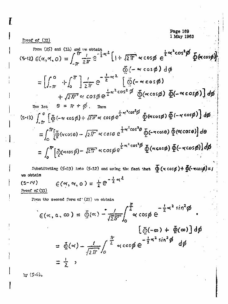
Page 169
1 May, 1963
P- o ,f-ora (25) 4 (14) an i; obtain
f 4,$- :<h~cs eo os 1 5() I -I - _
°7 0l ) , 4I 0_ C 0s e
i3-i- cs�')+ a Ccose• o ) •
,-c•c'<.o SO) Ccoo)J id
-, 4~' aI :[ ¢_ olco.. •'7.<slSe' .~co2 ~(acos•6) t(-.c s)I
i. -.g:Lot :<o~ 71,<•,,I-- lzCOSI-0
ia•e obtain
ý s-,13) -0. Cs, r2,?; ( CO 0 - e-(C:•O
PCoo* O SN(33) , Oe o s 4
i! ~From th2 second ror V£' (27) '•. obto'•iti
• ( qr c o ) -- J/ o•<<) -os e os
F<•-:>4 cos e'co) <
I L
I. Jf e 2.
F~roof Of (3f
Frmtbiiseodf- f(2)-noti

cPage 1701 May 1963
.. zm e, O f ( - 4
F~rm the, saor-4 form, of (27) we ha-o four CL--O C CL 71 0• O c > 0;
_ eL._ • - I• osine"a,• a c,-,o e7510.
qq aoý
- a o• - , ed/* 0 o sin •
i~C Cos-- cs ICt Co
II

Page 1711 May 1963
Tinn
elf~ sin zo
cx Cos (0eZ
(co o)
FzWr. (26) and (5-17) vactirr c C. 0. > C) c<0
Li)(il r" c~c L cYt 0- ____ (c<
a.
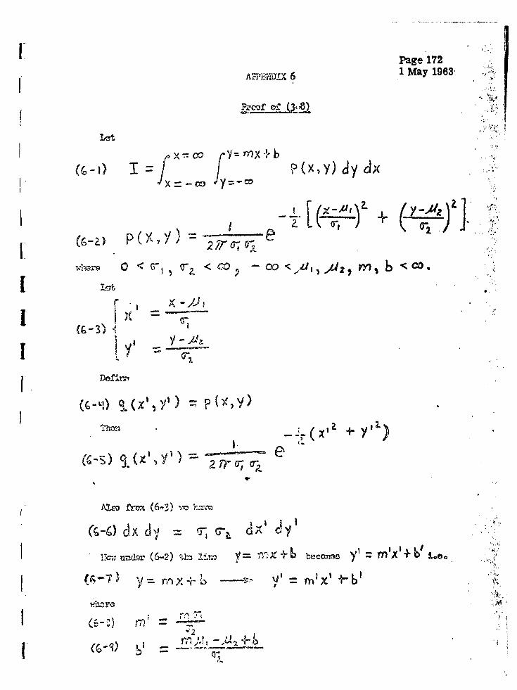
I Page 172Ir A -;:Yu.Ex 6 .1 May 1963.
(s-) pO),Ywhere 0 <~fy= o~ddV,~O
Also tr-i(& 3)io .
( c-l c cl' - G d
i~z.'(6-2) +A ~ ' becomao yl +n, +b ~o~o
- rn 6

Page 1731 May 1963
Thouý6-) 7-.t
Ilm Il ro ntc'
F~TF
Dmle

Page 1741 May 1963
.A1H ,IX 0 ,, ro 0 .
beams• iie
A,^JO fx',m (6-,2), i
(e~ x y - (jI d JIxJ'I
+ Y,
10
I
+ M
(A-7) b-'
I,/ .v r/X'=O I , r x! (&-'t,) I 'y= •4 •, ""
- •- _(• ,--- ,•
! .
.. * , j ;< -j: • o .! i1

Page 1751 May 60,q33
I4.-
/04
4 6 1
II /0t
____- - 4 db 3.14h
1 ~0/
o,234 5'6 78 9 /0 // 12 A (46)
with Quadrature Distortion as Parameter

Page 1761 May 19(q;ý
14)
K.
ItI
a 0
Figure 2. Inserted Carrier Phase Jitter vs. QuadratureDistortion with SSB Error Rate as Parameter

fU
Page 177
1May I,
/ -
A "- 20
: • I TQ /WV-PhM95E COMPONENT
/ 7.a •d6.c =EQU/V~q4.6WT S/Al /i
1i4.90 INRTEV C9d.6ER
* r'ms Ph'/Q5E Jt77TEZ
/I' Tq/F I/M5/-LTcE
13.2 /0 VA T/o0R
I , 0 D FRM P4.5
T0"'g • RES4'" A ,E , ,v'6
-30 -O -/0 0 /0 20 30
.. 5 ./ Z 5 1 /0 I5 209530 /
Figure 3. SSB Error-Rate vs. Quadrature Distortion withInserted Carrier Phase Jitter as Parameter
I

I
Page 178
j 1 May 1963
Iuod~f., \ , xO&9:
DIAAFREAMM ASK s
4:A~~ (d,6)__
I
5 /7db /0 ' 5 /
_______0 C9omon/4,9n
! ' .. . .. . .. ..I -. ..
I , - t.,,/.
"/1db 15
0 /0 20D 30 40 50 •
2 5 /0 20O304050 /00 500/I000
'1 Figure 4. SSB Error-Ra.te vs. S/N'1n Signal Channel with Inserted
Carrier Phase Jitter as Parameter, Assuming Zero
r Quadrature Component

IPage 1791 May 1963
I , .. % •. >. >• S N ,)".u ON S *0 (RDAS
I .......
0 -
Ioi
I - ..... . . .. - ... .. ...
I Figure 5. RMS Phase Jitter in the Inserted Carrier vs.Equivalent S/N in the Inserted Carrier
I
1:

Page 1801 May 1963
10 RfverS., Ko Ho, "'The- Coiqtab13ity PrOb3mi In SjWugjlmSjG~jd TrnM wmm
?M88LOI PrOceedaius of the Ir.~ hgmt~ 1960O9 papaWB 1.2a.1O,
20 DugMvdji, 4.9 "Envelopesanmd ft&4m1-A~pes of ReWl Waveftrm,a"
fltI Traiuactions on Inibrmti~a1on 1¶ory, Mwarc 1958.9 pages 5~3-57*
I ~3o Wlcdletonp Dos "An Introduction Tb Sttctistical O!memicat~Lon
Theoryp" Xqcrau-Hna3 2960o,
4~,? Deutsch, Rog "?0onhinear Transfornatiorns of Random Prooeacea."
I ~Prenti.oe-Ha11, 1962,,
5o Schwartz~, Hog "Ingbroation TraZI3RhLBi.on Nothgationg Wn Iboises"
6*- National Bmrau of Stauidardsm ."Tables of the M~varlato NormQg.
flatriibtion Function and Relat~ed Fmetomg," A~pplied Mathcxiatdiol
Sarlans116 5~0 .~9 1959.

!Page 181[ 1 May 1963
I- BIBLIOGRAPHY
I 1. "The Computation of SSB Peak Power't - Squires, Bedrosian, Proc.IRE Jan. 1960, pg. 123.
2. "Communication Efficiency Comparison of Several Communication
Systems" - Sanders, Proc. IRE April 1960, pg. 575.
3. "Combined AM & PM for a one-sided spectrum" - Taylor, Proc. IREMay 1960, pg. 953.
4. "Noise Spectrum of Phase-Locked Oscillators" - Strandberg, Proc.
IRE June 1960, pg. 1168.!5. "Increasing the Dynamic Tracking Range of Phase-Locked Loop" -
Weaver, Proc. IRE May 1960, pg. 952.I6. "The Compatibility Problem in SSB Transmission" - Powers, Proc.IRE Aug. 1960, pg. 1431.
7. "Noise in Oscillators" - Edson, Proc. IRE Aug. 1960, pg. 1454" '' ''Mullen ' ' ' " " 1467SGolay 1473
8. "Poisson, Shannon & the Ham" - Basly, Costas Proc. IRE, Aug. 1960,"f pg. 1495.
9. "The Compatibility Problem in SSB" - Kahn, Proc. IRE Aug. 1960,I pg. 1504.
10. "High Sblectivity with Constant Phase Over the Pass Band" - Rihaczek,Proc. IRE Oct. 1960, pg. 1756.
11. "Automatic Phase Control Theory & Design" - Rey, Proc. IRE, Oct.1960, pg. 1760.
12. Correction to "A New Iook at the Phase-Locked Oscillator' - McAllen,Proc.IRE Oct. 1940, pg. 1771.
13. "Interrelation and CombivUtion of Various Types of Modulation" -Meewezen, Proc. IRE Nov. 1960, pg. 1824.
I

IPage 1821 May 1963
14. "Traffic Efficiencies in Congested Band Radio Systems" - Weber,Costis, Proc. IRE Nov. 1960, pg. 1910.
15. "Regenerative Fractional Frequency Generators" - Plotkin, Lumpkin,Proc. IRE Dec. 1960, pg. 1988.
16. "Evaluation of Modulation Methods for Tange Telemetry" - Rudin, IREConvention Board - 1960, Part 5, pg. 17.
17. "Detection Levels & Error Rates in PCM Telemetry" - Balakrishnan,Abrams, IRE Convention Record - 1960, Part 5, pg. 37.
18. "Optimized SSB Transmitter Loading by Multichannel Freq. Division
Data" - Brennan, Daly, Goldberg, IRE Convention Record - 1960,Part 5, pg. 188.
19. "Electromagnetic Interference and Vulnerability Reduction" - J. J.Egli, IRE Convention Record - 1960, Part 8, pg. 48.
20. "Phase Stability of Oscillators" - Sann, Proc. IRE Feb. 1961, pg. 527.
21. "Correction to "APC Theory & Design" - Rey, Proc. IRE March 1961,pg. 590.
22. "SSB Communication" - Makris, Proc. IRE March, 1961, pg. 632.
23. "A Note on Instantaneous Spectrum" - Rothschild, Proc. IRE March1961, pg. 649.
24. "Dynamic Response of Rihaczek's Constant Phase Non-Linear Filter",Proc. IRE April 1961, pg. 822.
25. "A Method for Generating Signals of Arbitrary Yet Frequency -Independent Phase Differences" - Nilssen, Proc. IRE May 1961,pg. 964.
26. "Results of a Long Range Clock Synchronization Experiment" - Redes,Winkler, Bichart, Proc. IRE June 1961, pg. 1028.
27. "A Superposition Property of Angle Modulation" - Goodman, Proc.IREJune 1961, pg. 1084.
!
!

Page 1831 May 1963
"| 28. "A Mechanism for Direct Adjacent Channel Interference" - Ruthroff,Proc. IRE June 1961,pg. 1091.
S29. ".Discussion of Combined AM & PM for a One-Sided Spectrum" -Golden, et al, Proc. IRE June 1961, pg. 1094.
30. "Pull-in Frequency of the Phase-Controlled Oscillator" - Goldstein & IByrne, Proc. IRE July 1961, pg. 1209.
L 31. "Receivers with Zero IF" - Rubin, Proc. IRE Aug. 1961, pg. 1327.
j 32. "Compatible SSB" - Kahn, Proc. IRE Oct. 1961, pg. 1503.
33. "The Linearized Transfer Function of a Phase-Locked Loop-Containingi an IF Amplifier"- Lowhorn, Weaver, Proc. IRE Nov. 1961, pg. 1704.
34. "A Static Electronic Frequency Changer" - Griffith, Ulmer, IRE Con-Svention Record 1961, Part 5, pag. 342.
35. "Voice Modulated SSB and DSB Peak to Average Envelope PowerI Ratios" - Griffiths, IRE Convention Record 1961, Part 8, pg. 84.
36. "Analysis of Multiple Tone Clipping" - Styers, IRE Convention Record1 1961, Part 8, pg. 134.
37. "The Dwindling HF Spectrum" - Jacobs, Martin, IRE Convention IRecord -I 1961, Part 8, pg. 179.
38. "Performance of a 640 Mile, 24-channel UHF-SSB System" - Nichols,Trans. PGCS, March 1960, pg. 26.
39. "Combined Digital Phase & AM Systems" - Cahn, PGCS, Sept. 1960,| pg. 150.
40. "FM & SSB Radiotelephone Tests on a VHF Ionoscatter Link DuringMultipath Conditions" -Koch, Harding, Jansen, PGCS, Sept. 1960,pg. 183.
44L "Military Radio Communications Equipment Cost-Design Relation-ships" - Ports, et al. PGCS, Dec. 1960, pg. 203.-
[
[!

IPage 184"1 May 1963
S42. "Distortion of Angle - Modulated Systems in Misaligned LinearFilters" Galejs PGCS, Dec. 1960, pg. 228.
43. "Performance of Combined AM & PM Systems" - Hancock, Lucky,PGCS, Dec. 1960.
44. "Precision Frequency Control for Military Applications" - Gerber,Hand, PGMIL, Oct. 1960, pg. 424.i
45. "Multichannel Radio Communication Within the Army" - L. G. Fobes,PGMIL, Oct. 1960, pg. 505.
46. "Energy Spectra of FM System with Low /1, Hi-Deviation Ratio, and.MG Which Approaches Carrier Frequency" - Simmons, PGSET,
SMarch 1960, pg. 17.
47. "Threshold Improvement in an FM Subcarrier System" - Martin PGSET7March 1960. pg. 25.
48. "The Case of FM-AM vs. FM-PM Telemetry" - Rauch, PGSET,1 June 1960, pg. 81.
49. "The Effect of Different Types of Video Filters on PDM-FM andPCM-FM Radio Telemetry" - Nichols, Bublitz, PGSET, June 1960,pg. 85.
50. "Considerations on Synch. for PCM Telemetry" - Rauch, PGSET,Sept.-Dec. 1960, pg. 94.
51. "PCM/FM Telemetry Signal Analysis and Bandwidth Effects" - Ormsby,PGSET, Sept. -Dec. 1960, pg. 129.
I 52. "A Comparison of Wideband and Narrowband Mobile Circuits at 150Mc" - Nylund, PGVC, May 1960, pg. 69.
I53. "Can SSB Provide More Usable Channels in the Land Mobile Service?"-
Korolenko, Shepherd PGVC, Aug. 1960, pg. 47.
i 54. "Study by RMA-RTMA - TR 8. 9 (1877-A-1) 1946 Mobile VehicularSytems - Geographical Pattern of Frequency Assignments foe-MebileSystems Near 150 Mc."
I.
I

Page 1851 May 1963
55. "Adjacent Channel and the Courier Curse" - Smith PGVC, June 1957.
56. "Application of SSB For Mobile Communication" - Firestone, Magnuski,PGVC-11, 1948, pg. 48.
57. "The Gaussian Curse - XMTR Noise Limits Spectrum Utilization" -Shepherd, Smith, PGVC-10, April 1948, pg. 27.
58. "Channel Spacing Considerations in the 154-174 MC Band" - Strauss,PGVC, June 1952, pg. 44.
59. "Choosing the Optimum Type of Modulation - A Comparison of SeveralSystems of Comm." - Kelly, PGCS-6, June 1958, pg. 14.
60. "Poisson, Channon, and the Radio Amateur" - Costas, Proc. IREDec. 1959, pg. 2058.
S61. "Receivers With Zero IF" - Greene & Lyons, Proc. IRE Feb. 1959,pg. 335.
j 62. "Progress and Problems in U.S. Army Communications" - Lacy,Proc. IRE May 1959, pg. 650.
63. "A Critical Analysis of Some Communications Systems Derived fromAM" - Nupp, Proc. IRE May 1959, pg. 697.
64. "A New Look at The Phase-Locked Oscillator" - McAllen, Proc. IREJune 1959, pg. 1137.
65. "FM Multiplex Spectrum and Interference" - Arguimbau, Proc.IREAug. 1959, pg. 1372.
66. "Combined AM & PM For a One-Sided Spectrum" - Chakrabarti,Proc. IRE Sept. 1959, pg. 1663.
67. "Short-Time Stability of a Quartz-Crystal Oscillator as Measured Withand Ammonia - Maser" - Morgan & Barnes, Proc. IRE Oct. 1959,pg. 1782.
68. "Crystal Noise Effects on Zero IF Receiver" - Andrews & Bazydlo,Proc. IRE Nov. 1959, pg. 2018.
F4

e 186
69. "Experience With SSB Mbbile EquipmentV - Richardson, Eness,i Dronsuth, Proc. IRE June 1957, pg. 823.
70. "On The Use of Ferrites For Microwave SSB Modulators" - Khoury,Proc. IRE Oct. 1957, pg. 1418.
71. "DSB vs. SSB Systems" - Costas, Proc. IRE April 1957, pg. 534.
72. "SSB Performance As a Function of Carrier Strength" - Shepherd,Proc. IRE April 1957, pg. 541.
1 73. "A Simplified Method for Designing Wideband High Precision 900 PhaseNetworks" - Lerner, R. M., MIT Lincoln Lab Group Report 36-40,
1 Aug. 7, 1959.
74. "Wideband Phase Shift Networks" - R. B. Dome, Electronics, Dec.[ 1946, pg. 112.
75. "The Serrodyne- Frequency Translator" - R.C. Cummings, Proc. IRE,1 Feb. 1957.
76. "A Microwave SSB Modulator" - H. G. Pascalar, MIT Lincoln LabGroup Report No. 8, April 22, 1958.
77. '"Deeign of a Broadband Microwave SSB Generator" - J. P. Dougherty,RCA TR-62-564-2, (GE&D #998690, Co. Private ).
78. "Iroperties of Some Wideband Phase - Splitting Networks" - D.G. C.Luck, Proc. IRE, Feb. 1949.
79. "Realization of a Constant Phase Difference" - S. Darlington, B.S.T.J.
Jan. 1950.
80. "Synthesis of Wideband Two-Phase Networks" - H. J. Orchard, Wire-I less Engineer, March 1950.
1. "Cascade Connection of 90-Degree Phase Shift Networks" - 0. G.S-Uillard Jr., Proc. IRE, March 1952.
82. "Standardization of the Transient Response of Television Transmitters" -1 Kell & Fredendall, RCA Review, March 1949.
I
[

Page 187I1 May 1963
83. "Phase and Amplitude Equalizer for Television Use" - Goodale andKennedy RCA Aview, March 1949.
84. "Selective Sideband Transmission in Television" - Kell and Fredendall,RCA Review, April 1940.
85. "Selective Sideband vs. Double Sideband Transmission of Telegraph andFacsimile Signals" - Smith, Trevor, Carter, RCA Raview, Oct. 1938.
86. "Certain Topics in Telegraph Transmission Theory" - H. Nyquist, BTL
Mono. #B-331, August 1928.
87. "An AM Vestigial Sideband Data Transmission Set Using SynchronousDetection for Serial Transmission Up to 3,000 Bits per Second" -Becker, Davey, Saltzberg, Communication and Electronics, May 1962.
88. "Theoretical Fundamentals of Pulse Transmission" - Sunde, BSTJ,I May 1954, July 1954.
89. "Ideal Binary Pulse Transmission by AMAnd FM" - Sunde, BSTJ,J Nov. 1959.
90. "Pulse Transmission by AM, FM and PM In the Presence of PhaseSDistortion" - Sunde, BSTJ, March 1961.
91. "Sage Data Terminals" - Soffel, Spack, AIEE Trans. Pt. 1 (Commuri-cation and Electronics) vol 77, 1958 (Jan. 1959 section).
92. "Digital Data Fundamentals and the Two Level Vestigial SidebandSystem for Voice Bandwidth Circuits" - Hollis, WESCON Cony.Record, Vol. 4, Part- , 1960.
93. "Synchronous Communications" - Costas, Proc. IRE, Dec. 1956.
I 94. "Phase Reversal Data Transmission System for Switched and PrivateTelephone Line Applications"- Hopner, IBM Journal of Research andDevelopment, April 1961.
I 95. "The L-s Coaxial System - TV Terminals" - Rieke, Graham, BSTJ,July 1953.
S96. "Theory of AFC Synchronization" - Gruen Proc. IRE, August 1953.
I
l'

Page 188
[ 1 May 1963
97. "Data System Tests Using Simulated Transmission Impairments" -Andrevs, Communication and Electronics, Vol. 80, 1961 (Jan 1962
i section).
98. "Capabilities of the Telephone Network for Data Transmission" -
Alexander, Grvb, Nast, BSTJ, May 1960.
99. "Design and Performance of Phase-Lock Circuits Capable of Near-I Optimum Performance Over a Wide Range of Input Signal and Noise
Levels" - Jaffe, Rechtin, Trans. PGIT, March 1955.
100. "Frequency Economy in Mobile Radio Bands" - Bullington, BSTJ,Jan. 1953.
S101. "Intermodulation Interference in Radio Systems" - Babcock, BSTJ,Jan. 1953.
102. "Reduction of Bandwidth' Requirements for Radio Relay Systems" -
Mack, Meyerhoff, Jacoby, Levine, IRE Conv. ke~ord, Part 8, 1958.
103. "Practical Considerations in the Design of Minimum Bandwidth DigitalFM Systems Using Gaussian Filtering" - Glomb, Trans. PGCS,Dec. 1959.
104. "Gaussian Response Filter Design" - Dishal, Electrical Communica-
tion, Vo. 36, No. 1, 1959.
105. "A Simple Wideband 900 Phase Splitter for Speech or Music" -L. V. Kriger, AFCRL 930, Oct. 1961, AD 271757.
106. "Radio Propagation Variations at VHF and UHF"' - K. Bullington,Proc. IRE, Jan. 1950.
107. "Study of I-F Transformers for SSB Operation" - Ill. Inst. of Tech.,Feb. 1, 1960 to Oct. 31, 1962 FINAL Report.
108. "Ferroelectric Ceramic Filters, IF Transformers, And Networks" -Koneval, Curran. Report #23, DA-36-039-sc-87275, Clevite Corp.,30 June 1962. AD-282835.
109. "Phase-Lock Loop Frequency Acquisition Study" - Frazier, Page,Trans. PGSET, Sept. 1962.
110. "Comparison of Split Channel FM & SSB For Land Mobile Services" -A. A. MacDonald, PGVC, Dec. 1956.
I

[ Page 189
DISTRIBUTION LIST
OASD (RUE), Rm 3E1065ATTN: Technical LibraryThe PentagonWashington 25, D. C.
Chief of Research and Development
OCS, Department of the ArmyWashington 25, D. C.
Commanding GeneralU. S. Army Materiel CommandATTN: R&D DirectorateNyashington 25, D. C.
Commanding GeneralU. S. Army Electronics CommandATTN: AMSEL-ADFort Monmouth, N.J. 3
f Commander, Armed Services TechnicalInformation Agency
ATTN: TISIAj Arlington Hall Station
Arlington 12, Virginia 10
Commanding GeneralUSA Combat Developments CommandATTN: CDCMR-EFort Belvoir, Virginia
Commanding OfficerUSA Communication and Electronics
Combat Development AgencyFort Huachuca, Arizona
Commanding GeneralU. S. Army Electronics Research andI Development ActivityATTN: Technical LibraryFort Huachuca, Arizona
Chief, U. S. Army Security AgencyArlington Hall StationArlington 12, Virginia 2
I

Page 190
(~ 1may 1963
Deputy PresidentU. S. Army Security Agency BoardArlington Hall StationArlington 12, Virginia 1iCommanding OfficerDiamond Ordnance Fuze Laboratories
SATTN: Library, Rm. 211, Bldg. 92Washington 25, D. C. 1
j Director, U. S. Naval Research LaboratoryATTN: Code 2027Washington 25, D. C. 1
Commanding Officer and DirectorU. S. Navy Electronics LaboratorySan Diego 52, California 1
Aeronautical Systems DivisionATTN: ASAPRLWright-Patterson Air Force Base, Ohio 1
F Air Force Cambridge Research LaboratoriesATTN: CRZCL. G. Hanscom Field
| Bedford, Massachusetts 1
Air Force Cambridge Research LaboratoriesATTN: CRXL-RL. G. Hanscom Field
I Bedford, Massachusetts
Hq. Electronic Systems DivisionATTN: ESATL. G. Hanscom FieldBedford, Massachusetts
I AFSC Scientific/Technical Liaison OfficeU. S. Naval Air Development Center[ Johnsville, Pennsylvania 1
Commanding OfficerU. S. Army Electronics Materiel Support AgencyATTN: SELMS-ADJFort Monmouth, New Jersey 1r
I

Page 191[ -. 1 May 193
Director, Fort Monmouth OfficeUSA Communication and Electronics
Combat Development AgencyFort Monmouth, New Jersey
I Corps of Engineers Liaison OfficeU. S. Army Electronics Research & Develop-
ment LaboratoryFort Monmouth, New Jersey
I Marine Corps Liaison OfficeU. S. Army Electronics Research &
Development Laboratory[ Fort Monmouth, New Jersey 1
AFSC Scientific/Technical Liaison OfficeI U.S. Army Electronics Research &Development Laboratory
Fort Monmouth, New Jersey 1!Commanding OfficerU. S. Army Electronics Research & Develop-
I ment LaboratoryATTN: Logistics Division, MARKED FOR James BaileyFort Monmouth, New Jersey 8ICommanding OfficerU. S. Army Electronics Research & Development
LaboratoryATTN: Director of Research/EngineeringFort Monmouth, New Jersey 1
Commanding OfficerU. S. Army Electronics Research & Development
LaboratoryATTN: Technical Documents CenterFort Monmouth, New Jersey 1
Commanding OfficerU. S. Army Electronics Research & Development LaboratoryI ATTN: SELRA-NR-5Fort Monmouth, New Jersey 1
( Commanding OfficerU. S. Army Electronics Research & Development LaboratoryATTN: Technical Information Division
SFort Monmouth, New Jersey 3
I