Debug Port Design Guide for UP/DP Systems - Intel€¦ · debug port design guide for up/dp systems...
42
Order Number: 313373-001 Debug Port Design Guide for UP/DP Systems June 2006
Transcript of Debug Port Design Guide for UP/DP Systems - Intel€¦ · debug port design guide for up/dp systems...

Order Number: 313373-001
Debug Port Design Guide for UP/DP Systems
June 2006

2 DPDG for UP/DP Systems Order Number: 313373-001
Legal Lines and Disc laimersIINFORMATION IN THIS DOCUMENT IS PROVIDED IN CONNECTION WITH INTEL® PRODUCTS. NO LICENSE, EXPRESS OR IMPLIED, BY ESTOPPEL OR OTHERWISE, TO ANY INTELLECTUAL PROPERTY RIGHTS IS GRANTED BY THIS DOCUMENT. EXCEPT AS PROVIDED IN INTEL'S TERMS AND CONDITIONS OF SALE FOR SUCH PRODUCTS, INTEL ASSUMES NO LIABILITY WHATSOEVER, AND INTEL DISCLAIMS ANY EXPRESS OR IMPLIED WARRANTY, RELATING TO SALE AND/OR USE OF INTEL PRODUCTS INCLUDING LIABILITY OR WARRANTIES RELATING TO FITNESS FOR A PARTICULAR PURPOSE, MERCHANTABILITY, OR INFRINGEMENT OF ANY PATENT, COPYRIGHT OR OTHER INTELLECTUAL PROPERTY RIGHT. Intel products are not intended for use in medical, life saving, life sustaining, critical control or safety systems, or in nuclear facility applications.
Intel may make changes to specifications and product descriptions at any time, without notice.
Designers must not rely on the absence or characteristics of any features or instructions marked "reserved" or “undefined.” Intel reserves these for future definition and shall have no responsibility whatsoever for conflicts or incompatibilities arising from future changes to them.
The Debug Port Design Guide for Product Name Systems may contain design defects or errors known as errata which may cause the product to deviate from published specifications. Current characterized errata are available on request.
Contact your local Intel sales office or your distributor to obtain the latest specifications and before placing your product order.
I2C is a two-wire communications bus/protocol developed by Philips. SMBus is a subset of the I2C bus/protocol and was developed by Intel. Implementations of the I2C bus/protocol may require licenses from various entities, including Philips Electronics N.V. and North American Philips Corporation.
Intel and the Intel logo are trademarks or registered trademarks of Intel Corporation or its subsidiaries in the United States and other countries.
*Other names and brands may be claimed as the property of others.
Copyright © 2006, Intel Corporation.
Notice: This document contains information on products in the design phase of development. The information here is subject to change without notice. Do not finalize a design with this information.

DPDG for UP/DP Systems Order Number: 313373-001 3
Contents
1 How to Use this Document.............................................................................................7
2 Overview.....................................................................................................................92.1 General Guidelines ..............................................................................................9
2.1.1 Termination Resistors ............................................................................. 10
3 XDP Design Guide....................................................................................................... 133.1 Conventions ..................................................................................................... 133.2 XDP Routing Overview ....................................................................................... 133.3 JTAG Routing Guidelines..................................................................................... 16
3.3.1 TDI - TDO Routing Guidelines ................................................................. 163.3.2 TCK0 Routing ........................................................................................ 183.3.3 TMS Routing Guidelines........................................................................... 183.3.4 TRSTn Routing Guidelines........................................................................ 18
3.4 Run Control Routing Guidelines ........................................................................... 193.5 System Control Routing Guidelines ...................................................................... 19
3.5.1 PWRGOOD (HOOK0) Routing Guidelines .................................................... 193.5.2 Reserved (HOOK[1])............................................................................... 193.5.3 Reserved (HOOK[2])............................................................................... 193.5.4 Reserved (HOOK[3])............................................................................... 193.5.5 ITPCLK/ITPCLK# (HOOK[4:5]) Routing Guidelines ...................................... 193.5.6 RESET_IN# (HOOK6) Routing Guidelines ................................................... 203.5.7 RESET_OUT# (HOOK7) Routing Guidelines ................................................ 203.5.8 XDP_Present.......................................................................................... 20
3.6 I2C* Routing Guidelines ..................................................................................... 203.7 Observation Port Routing Guidelines .................................................................... 21
3.7.1 Observation Port Configurations ............................................................... 213.7.2 Observation Port Routing......................................................................... 213.7.3 OBSFN_x[1:0] ....................................................................................... 213.7.4 OBSDATA_A[3:0] ................................................................................... 22
3.7.4.1 Routing Guidelines .................................................................... 223.7.5 OBSDATA_B[3:0] ................................................................................... 22
3.7.5.1 Routing Guidelines .................................................................... 223.8 Power .............................................................................................................. 22
3.8.1 VCC_OBS Pins ....................................................................................... 223.8.2 Ground ................................................................................................. 22
3.9 System Connection............................................................................................ 223.10 Depopulating XDP for Production Units ................................................................. 243.11 Mechanical Specifications ................................................................................... 24
4 XDP-SSA Design Guide................................................................................................ 274.1 Conventions ..................................................................................................... 274.2 XDP-SSA Routing Overview ................................................................................ 274.3 JTAG Routing Guidelines..................................................................................... 27
4.3.1 TDI - TDO Routing Guidelines .................................................................. 274.3.2 TCK0 Routing ........................................................................................ 27
4.3.2.1 TMS Routing Guidelines ............................................................. 274.3.3 TRSTn Routing Guidelines........................................................................ 28
4.4 Run Control Routing Guidelines ........................................................................... 284.5 System Control Routing Guidelines ...................................................................... 28
4.5.1 PWRGOOD (HOOK0) Routing Guidelines .................................................... 284.5.2 Reserved (HOOK[1:3])............................................................................ 284.5.3 ITPCLK/ITPCLK# (HOOK[4:5]) Routing Guidelines ...................................... 284.5.4 RESET_IN# (HOOK6) Routing Guidelines ................................................... 28

4 DPDG for UP/DP SystemsOrder Number: 313373-001
4.5.5 RESET_OUT# (HOOK7) Routing Guidelines.................................................284.6 I2C* Routing Guidelines .....................................................................................284.7 Observation Port Routing Guidelines.....................................................................28
4.7.1 OBSFN_A[1:0] .......................................................................................294.7.2 OBSDATA_A[3:0] ...................................................................................29
4.8 Power ..............................................................................................................294.8.1 VCC_OBS Pins........................................................................................294.8.2 Ground..................................................................................................29
4.9 System Connection ............................................................................................294.10 Depopulating XDP-SSA for Production Units...........................................................304.11 Mechanical Specifications....................................................................................30
5 ITP700Flex Design Guide .............................................................................................335.1 Conventions......................................................................................................335.2 ITP700Flex Routing Overview ..............................................................................335.3 JTAG Routing Guidelines .....................................................................................35
5.3.1 TDI - TDO Routing Guidelines...................................................................355.3.2 TCK Routing...........................................................................................355.3.3 TMS Routing Guidelines ...........................................................................355.3.4 TRSTn Routing Guidelines ........................................................................355.3.5 FBO ......................................................................................................355.3.6 Run Control Routing Guidelines.................................................................35
5.4 System Control Routing Guidelines.......................................................................355.4.1 Reserved (HOOK[0:3]) ............................................................................365.4.2 ITPCLK/ITPCLK# (HOOK[4:5]) Routing Guidelines.......................................365.4.3 RESET_IN# (HOOK6) Routing Guidelines ...................................................365.4.4 RESET_OUT# (HOOK7) Routing Guidelines.................................................36
5.5 Observation Port Routing Guidelines.....................................................................375.5.1 Observation Port Routing .........................................................................375.5.2 OBSFN_x[0:1]........................................................................................37
5.6 Power ..............................................................................................................375.6.1 VTT, VTAP .............................................................................................375.6.2 Ground..................................................................................................37
5.7 System Connection ............................................................................................375.8 XDP Tools to ITP700Flex Adapters........................................................................385.9 Mechanical Specifications....................................................................................38
A Appendix A – Debug Port Interposer Considerations ........................................................41

DPDG for UP/DP Systems Order Number: 313373-001 5
Figures2-1 End Termination................................................................................................ 112-2 Middle Termination ............................................................................................ 113-1 XDP UP Routing Overview................................................................................... 143-2 XDP DP Routing Overview................................................................................... 153-3 TDI - TDO Routing for UP Systems ...................................................................... 163-4 TDI - TDO No Bypass Routing for DP Systems ....................................................... 163-5 TDI - TDO Jumpered Bypass Routing for DP Systems ............................................. 173-6 TDI - TDO Automatic Bypass for DP Systems ........................................................ 183-7 BPM[4:5] Routing.............................................................................................. 213-8 XDP Connector System Keepout Diagram ............................................................. 254-1 XDP-SSA Connector System Keepout Diagram ...................................................... 315-1 ITP700Flex Routing Overview.............................................................................. 345-2 ITP700Flex Connector System Keepout Diagram.................................................... 395-3 Top View of Surface Mount ITP700Flex................................................................. 39
Tables3-1 XDP Pinouts...................................................................................................... 234-1 XDP-SSA Pinouts............................................................................................... 305-1 ITP700Flex Debug Port Pinout ............................................................................. 38

6 DPDG for UP/DP SystemsOrder Number: 313373-001
Revision History
§
Document Number
Revision Number Description Date
313373 -001 • White Cover Release June 2006

DPDG for UP/DP Systems Order Number: 313373-001 7
How to Use this Document
1 How to Use this Document
This document's primary role is to distribute all of the best-known methods relating to the design of a debug port in Product Name processor based target systems. This document provides implementation details specific to these designs only and takes priority over any discrepancies existing between this document and any previous Debug Port Design Guide.
The details of this document are to be considered requirements for a debug port design, unless the text explicitly states that a design rule or connection is optional.
§

How to Use this Document
8 DPDG for UP/DP Systems Order Number: 313373-001

DPDG for UP/DP Systems Order Number: 313373-001 9
Overview
2 Overview
The debug port is a connection into a target system environment that provides access to JTAG, run control, and in some cases system control resources. Debug ports come in three styles; XDP, XDP-Sinned ITP700Flex.
The eXtended Debug Port (XDP) is a 60-pin, small form factor connector, and is the recommended implementation as it provides for additional silicon / system debug resources compared to other debug port implementations and provides for expansion for future capabilities. Using XDP could save valuable time if debug by Intel is required. Most commercially available run control tools only interface to the XDP port.
Additionally XDP extends JTAG by permitting implementation of two separate clock domain scan chains. The goal of dividing the system scan chains into two domains is to increase the operating frequency of the processor scan chain by moving the typically slower chipset JTAG agents to a completely separate clock domain. This was not possible using ITP700Flex or the previous generation of run control tool hardware. XDP also provides assistance in management and debug of power, reset and clocking.
For design guidelines with XDP, see the guidelines in this chapter and also Section 3, “XDP Design Guide” on page 13
XDP-SSA (Second Side Attach) is a 31-pin alternative to XDP for those customers needing to place the debug port on the non-component side of the board. XDP’s fine pitch has historically not fared well in a hand soldered environment. As there are fewer pins, XDP-SSA has less capabilities than XDP, primarily in that it only has a single Observability Port.
Use of the XDP-SSA connector in board designs will require the use of an XDP to XDP-SSA adapter during system debug. Contact the debug tool vendor for information on this adapter.
For design guidelines with XDP-SSA, see the guidelines in this chapter and also Section 4, “XDP-SSA Design Guide” on page 27
ITP700Flex is a slightly smaller form factor, 28-pin interface with a significantly smaller connection keep-out volume. ITP700Flex only allows for JTAG, run control and small amounts of system control resources. It does not allow for SMBUS support. The maximum speed of an ITP700Flex implementation is also limited compared to the XDP implementation.
For design guidelines for ITP700Flex, see Section 5, “ITP700Flex Design Guide” on page 33.
2.1 General Guidelines
These guidelines apply to XDP designs, XDP-SSA and ITP700Flex designs.
For some signals, the existence of on-die termination (ODT) within the processor or chipset will remove parts from the platform design. The processor or chipset specific datasheet will clarify if ODT exists on signals from this design guideline.

Overview
10 DPDG for UP/DP Systems Order Number: 313373-001
Electrical lengths are provided in units of flight-time. Conversion of flight time to board trace lengths is dependent on what layer routing occurs on, and the dielectric constant of the board materials for a specific design. Rule of thumb numbers can be derived by using 140-180ps/inch for outer layers of an FR4 product and 180ps/inch for inner layers.
All JTAG and BPM# signals must be routed using 45-65 ohm +/-10% impedance traces. The length of any unterminated stub on any of these nets must be less than 200ps unless otherwise stated. JTAG and BPM# signals may optionally be terminated using the nominal board impedance. The 51 +/- 5% ohm recommendation in this document has been proven to work on all board impedances tested to date.
VTAP for single or dual processor systems will be the VTT rail (or system bus IO voltage) of the processors
In all drawings, signals that are not connected may be assumed to be left floating thus no termination is required.
All diagrams show the preferred implementation of passing a signal through the ball and out to a termination. However, because of breakout constraints within the processor zones a designer could T off the termination prior to the processor ball. In that case the stub to the processor cannot exceed 200pS in length.
TCK0, system clocks, and all of the observation pins should be routed with high-speed design rules in mind. In particular:
• An effort should be made to minimize the number of layer transitions and plane split crossings imposed on each trace (ideally this will be zero). If return paths are well kept then the number of vias are nearly immaterial. A good rule of thumb would be to use no more than 3 vias and/or spend extra effort to insure good return path currents.
• Keep the critical signals referenced to GND whenever possible.
• Include stitching vias near every layer transition. This is important even when referencing the same voltage on the new layer because the stitching via may reduce return current loops on the trace.
• Include a bypass capacitor near every layer transition or plane split between the two referenced planes.
• An effort should be made not to share XDP bypass capacitors with other high-speed signals.
• For all signals, pull-up termination resistors should be located above a solid power plane. If a solid power plane does not exist at the required termination location, add a 0.1uF ceramic capacitor to GND on the pull-up voltage within 0.5 inches of termination resistor.
2.1.1 Termination Resistors
Termination resistances are given with tolerances whenever appropriate. If given, tolerances are within +/- of the percentage given.
With few exceptions (noted specifically in their description), termination resistors must be close to the receiver. The topology at the end of the chain must be terminated in one of the following ways in all cases except those noted in their specific description.

DPDG for UP/DP Systems Order Number: 313373-001 11
Overview
In the case of Figure 2-1 where there is a termination after the last receiver, A must be smaller than any noted maximum routing length. This is the typical way of showing terminations in this document. There is no restriction for the length of B unless otherwise noted.
Another method for termination that is equally valid is a termination prior to the end receiver where the maximum routing length of the signal must be less than the length of D+C. C must be less than 200pS.
In both cases above note that there may be other devices on the A (or D) routing of the signal if called for within this document.
§
Figure 2-1. End Termination
Device
Receiver A
B
V
Device
Driver
Figure 2-2. Middle Termination
Device
Receiver
DC
V
Device
Driver

Overview
12 DPDG for UP/DP Systems Order Number: 313373-001

DPDG for UP/DP Systems Order Number: 313373-001 13
XDP Design Guide
3 XDP Design Guide
3.1 Conventions
Devices in a scan chain are enumerated by tracing TDI and the scan chain’s TCK from the XDP connector to the first device using both these signals. This device is device #0. Then, trace TDO from device #0 to TDI of device #1, etc.
The last device in the scan chain is found by tracing TDO from the XDP connector to TDO of the last device.
Special Note: TDI is an output of the debug port connector and TDO is an input of the debug port connector despite their nomenclature. The opposite is true of other JTAG devices: TDI is an input of other JTAG devices and TDO is an output.
3.2 XDP Routing Overview
This section contains a thumbnail sketch of how to connect all debug port signals except TDI/TDO in the simplest connection configuration. Please refer to the details of each signal for complete information. These drawings represent only the most basic connection.
TDO/TDI have a great number of options based on the number of processors in your system and if you are allowing empty sockets. Please see Section 3.3.1, “TDI - TDO Routing Guidelines” on page 16.
Note that any signal that is not noted on this drawing may be left as no connect.

XDP Design Guide
14 DPDG for UP/DP Systems Order Number: 313373-001
Notes:
A - These resistors will either be opens (if the processor has on-die termination) or 51 ohm 5% (if processor has no on-die termination)B - This routing length is unconstrained.C - Maximum routing of these signals are 1.5ns and must be length matched to one another within 50 ps.D - This routing length must be a maximum of 1.5ns. E - These traces have no specific routing length requirements. F - These traces lengths are determined by the driver and driver termination. G - This trace length must not exceed 200ps -- see the datasheet.I - This resistance is dependant on the front panel circuit receiver.Z - Source termination method is defined by the clock driver.
All signals not noted except TDI and TDO are to be left NC.
Figure 3-1. XDP UP Routing Overview
515%
Processor
BPM0#
BPM1#
BPM2#
BPM3#
BPM4# (PRDY)
BPM5# (PREQ)
TMS
TCK
TRST#
RESET#
PWRGOOD
eXtended Debug Port
VCC_OBS_CD
VCC_OBS_AB
OBSDATA_A3
OBSDATA_A2
OBSDATA_A1
OBSDATA_A0
OBSFN_A1
OBSFN_A0
TMS
TCK0
TRSTn
HOOK0
HOOK4
HOOK5
HOOK6
HOOK7
XDP PRESENT
GND
1K 5%
515%
Vtt
515%
A
A
A
A
Front Panel Reset
XDP detect circuit Clock Generator
ClkOut
ClkOut#
E
C
C
C
C
C
C
D
E
G E
B
B
B
B
E
B
E
E
F
F
E
B
1.5-3.3VDC
IE
Z
E
B
A
A
B
DPDG for UP/DP Systems Order Number: 313373-001 15
XDP Design Guide
Notes:
A - These resistors will either be opens (if the processor has on-die termination) or 51 ohm 5% (if processor has no on-die termination).B - This routing length is unconstrained.C - These must be a maximum length of 1.5ns and must be length matched to within 50ps of one another but not to K.E - Total length must be no more than 1.5ns. Each of these do not need to be length matched.F - Maximum trace routing of 200ps.G - There are no trace routing requirements for this signal.I - These traces lengths are determined by the driver and driver termination.J - This resistance and routing is dependent on the front panel circuit receiver.K - These must be no longer than 1.5ns and must be length matched to within 50ps of one another but not to C.M - There are no routing length requirements for this signal.Z - Source termination method is defined by the clock driver.
All signals not noted except TDI and TDO are to be left NC
Figure 3-2. XDP DP Routing Overview
Proc 0BPM0
BPM1
BPM2
BPM3
BPM4(PRDY)
BPM5(PREQ)
TMS
TCK
TRST#
RESET#
PWRGOOD
eXtended Debug Port
VCC_OBS_AB
OBSDATA_A3
OBSDATA_A2
OBSDATA_A1
OBSDATA_A0
OBSFN_A1
OBSFN_A0
TMS
TCK0
TRST#
HOOK0
HOOK4
HOOK5
HOOK6
HOOK7
XDPPresent
GND
VCC_OBS_CD
OBSFN_B1
OBSFN_B0
OBSDATA_B3
OBSDATA_B2
OBSDATA_B1
OBSDATA_B0
1K 5%
Vtt
A
A
A
A
Front Panel Reset
XDP detect circuit
ClkOut
ClkOut#
Clock
Generator
G
C
C
C
C
C
C
E
G
F G
B
B
B
B
J
I
I
G
1.5-3.3VDC
J
Vtt
K
K
K
K
K
K
515%
G
G
Proc 1
TRST#
TCK
TMS
BPM4(PRDY)
BPM5(PREQ)
BPM0
BPM1
BPM2
BPM3
EG
515%
A
A
A
A
Vtt
M
M
M
M
E
B
Vtt
515%
Z
A
A
B
B
M
M
A
A

XDP Design Guide
16 DPDG for UP/DP Systems Order Number: 313373-001
3.3 JTAG Routing Guidelines
3.3.1 TDI - TDO Routing Guidelines
Note: TDI is an output of the debug port connector and TDO is an input of the debug port connector despite their nomenclature. The opposite is true of other JTAG devices. TDI is an input of other devices and TDO is an output.
For UP systems using a single scan chain only, route TDI and TDO as indicated in Figure 3-3. There is no need for socket bypass capability
Notes:
A - These traces have no specific routing requirements. B - This routing has no length requirements.
For DP systems using a single scan chain with no intent to bypass a socket, route TDI and TDO as indicated below.
Notes:
A - These traces have no specific routing requirements. B - This routing has no length requirements.
Figure 3-3. TDI - TDO Routing for UP Systems
515%
Vtt
515%
B
Processor
TDI
TDO
XDP Debug Port
TDI
TDO
A
A
B
Figure 3-4. TDI - TDO No Bypass Routing for DP Systems
515%
515%
B
Proc0
TDI
TDO
XDP Debug Port
TDI
TDO
A
A
B
Proc1
TDI
TDO A
515%
B
Vtt
`
VttVtt

DPDG for UP/DP Systems Order Number: 313373-001 17
XDP Design Guide
Notes:
A - These traces have no specific routing requirements. B - This routing has no length requirements.
The four-pin bypass jumper can completely isolate a processor socket whenever the processor is not installed in the system. To include a processor load, place a jumper across pins 2 - 1 as well as pins 4-3. To remove a processor load simply jumper pins 2-4.
It is possible to replace the processor 4-pin bypass headers with Quick Switch* control gates and use the socket occupied signal to control the bypass condition. This topology is significantly different from the four-pin bypass header topology described earlier. This topology will use fewer components compared to directly translating the headers into Quick Switch* components. This topology also has the benefit of automatically causing an open circuit between TDI and TDO if both processors of one of the TDI – TDO chains are not occupied. These two bypass schemes have been designed to reduce stubs and to limit the number of pull-ups on any one net to two.
Quick Switch* components should be used for the MUX-DEMUX circuits in the figure below. These MUX-DEMUX circuits can either be created using individual Quick Switch* gates and inverters selectively used on the control signals, or through the use of Quick Switch* 2:1 MUX-DEMUX similar to Fairchild Semiconductor* NC7SB3157 – NC7SB3257 or equivalent.
Figure 3-5. TDI - TDO Jumpered Bypass Routing for DP Systems
515%
515%
B
Proc0
TDI
TDO
XDP Debug Port
TDI
TDO
B
Proc1
TDI
TDO
515%
B
Vtt
`
VttVtt
1 2
3 4
AA
A
1 2
3 4
A
A
A
A

XDP Design Guide
18 DPDG for UP/DP Systems Order Number: 313373-001
Notes:
A - These traces have no specific routing requirements. B - This routing has no length requirements.
3.3.2 TCK0 Routing
Route a scan chain TCK to each of its loads in a daisy chain fashion and then terminate with a 51 Ohm 5% resistor to GND at the processor end of the trace. The trace length for this signal must be a maximum of 1.5ns. Any stub on these nets must be shorter than 200ps. TCK0 should be routed to the CPU socket (UP) or both CPU sockets (DP). Device chains other than processor chains are not described in this document. Do not route TCK1 without contacting Intel for guidance.
3.3.3 TMS Routing Guidelines
TMS should be routed in a daisy chain fashion to each of the processors for a single scan chain. CPU0 should be first in the route, followed by CPU1 for DP systems. The TMS route for each scan chain should be terminated at the processor end with a 51 Ohm, 5% resistor to VTAP.
There is no trace length requirement for this signal.
3.3.4 TRSTn Routing Guidelines
This JTAG signal is routed as a daisy chain to all devices on all chains. There should be a 51 Ohm 5% pull down resistor on the trace. The location of this resistor is recommended to be near the last device in the chain with layout described in Section 2.1.1, “Termination Resistors” on page 10, but can be placed in other positions if necessary for platform layout. The trace length of this signal is unimportant.
Figure 3-6. TDI - TDO Automatic Bypass for DP Systems
515%
515%
B
Proc0
SKTOCC#
TDI
TDO
XDP Debug Port
TDI
TDO
B
Proc1
SKTOCC#
TDI
TDO
515%
B
Vtt
`
Vtt
Vtt
A
A
A
A
A
A
A
0
1
1
0
0
1A
A
A

DPDG for UP/DP Systems Order Number: 313373-001 19
XDP Design Guide
3.4 Run Control Routing Guidelines
Please see Section 3.7, “Observation Port Routing Guidelines” on page 21.
3.5 System Control Routing Guidelines
System Control operations report or manage the system power, scan, and reset states of the target system. These signals are HOOK[0:7] on the XDP debug port. HOOK[1:3] are generally left as no-connects.
3.5.1 PWRGOOD (HOOK0) Routing Guidelines
Route a system PWRGOOD signal directly to the XDP HOOK0 pin. This signal is used to indicate that the system’s power delivery subsystem has reached stability. This signal must be asserted before the run control tool will attempt operations. The run control tool will not drive PWRGOOD. The run control tool will use transitions on this signal as triggering events. Please consult the system’s Platform Design Guidelines (PDG) for termination information. If there is no PWRGOOD on system, pull this signal up to 1.0V-3.3V through a 1K-10K ohm resistor.
There are no trace length requirements for this signal.
3.5.2 Reserved (HOOK[1])
This signal is reserved. No connection to this signal are required.
3.5.3 Reserved (HOOK[2])
This signal is reserved. No connection to this signal is recommended.
3.5.4 Reserved (HOOK[3])
This signal is reserved. No connection to this signal is recommended.
3.5.5 ITPCLK/ITPCLK# (HOOK[4:5]) Routing Guidelines
A copy of the processor Front Side Bus Clock (usually BCLK[0:1]) needs to be delivered to the XDP by a system clock component. ITPCLK and ITPCLK# are used for noise and synchronizer fault survivability, and as a frequency reference for run control operations when enabled by the run control tool. Some run control and system interaction operations may be disabled if ITPCLK is not connected or unavailable.
Route differentially from the system clock distribution component to the HOOK[4:5] pins of XDP connector. Provide adequate source termination of the clock traces at the clock driver. Route the signals using the specification of the driver. There are no length matching requirements for this clock pair compared to any other signals in the target system.
Due to the variations in processor nomenclature, BCLK[0:1] is sometimes denoted as BCLK[p/n] respectively. Thus, BCLK[0] = BCLK[p] = ITPCLK = HOOK4 is the rising edge for the beginning of every transaction. Conversely, BCLK[1] = BCLK[n] = ITPCLK# = HOOK5.

XDP Design Guide
20 DPDG for UP/DP Systems Order Number: 313373-001
3.5.6 RESET_IN# (HOOK6) Routing Guidelines
The RESET_IN# signal is an input to the run control tool from the front-side bus RESET# signal. Run control tools will not drive RESET#; but uses this signal to sense when a system reset has occurred.
Route the front-side bus RESET# signal to the RESET_IN# pin through a 1Kohm isolation resistor. Routing of this signal before the isolation resistor is left to the system designers as part of the system design guides and datasheet. On the debug port side of the isolation resistor, this signal has no length requirement.
Rather than placing the isolation resistor within 200ps of the processor (as is shown in Routing Overviews), the isolation resistor would ideally be placed to remove any stub from the reset line by placing the isolation resistance pad directly at any point on the RESET# signal line. There is no requirement from the point of view of the run control tool but the system reset wired OR signal will have signal integrity issues with greater than a minimum stub.
Special Note for systems with Dual Independent Bus: As both Resets in the system are logically tied together (only a phase differential), the specific reset that HOOK6 is connected to is not material. Route whichever is easier for the system.
3.5.7 RESET_OUT# (HOOK7) Routing Guidelines
The RESET_OUT# signal is an output from the run control tool to the system reset control logic. The run control tool uses this signal to initiate a system reset. This reset assertion must not cycle any power supplies on the target system nor may it alter the PWRGOOD signal. The run control tool will drive this signal with a silicon switch closure to ground when a debug reset is requested.
Route this signal to any point within the system reset topology that would initiate the appropriate reset. Typical implementations route the RESET_OUT# signal to either a reset controller FPGA; to an OR function within the front panel reset circuit; or directly into the ICH signal SYS_RESET#. The pull up value and location is not critical to the run control tool but may be to the receiver or other drivers if this signal is wire-ORed.
The RESET_OUT# signal name may be referred to as DBR# (Debug Port Reset).
3.5.8 XDP_Present
This optional steady-state output from the run control hardware indicates the presence of an XDP style tool at the debug port. To use, the system will provide a pull-up termination of 1K to 10K ohm to this signal. Termination voltage for this signal can be to any voltage that is compatible with the receiver chosen by the platform design.
When XDP tool is present, the XDP tool will short this pin to ground.
3.6 I2C* Routing Guidelines
The I2C* interface from the XDP includes two pins – SDA and SCL. Route the XDP SDA pin to the SDA signal of the SM Bus on the system. Route the XDP SCL pin to the SCL signal of the SMBus on the system. The XDP I2C* interface is master only and cannot be slave addressed. The XDP I2C* master can be connected to any multiple-master I2C* bus within the target system that provides access to the hooks required for validation and debug. The debug port has no additional requirements for termination on these signals beyond the I2C* specifications.

DPDG for UP/DP Systems Order Number: 313373-001 21
XDP Design Guide
3.7 Observation Port Routing Guidelines
There are 4 observation ports on the XDP labeled A through D. Each observation port is made up of 4 OBSData lines and 2 OBSFN control/strobe lines.
These lines in the past have had historical names associated with them. The OBS_Port historically has been referred to as the BPM#[0:5] pins.
For reference: OBSFN_x0=BPM5#=PREQ#; OBSFN_x1=BPM4#=PRDY#; OBSDATA_x3=BPM0#; OBSDATA_x2=BPM1#; OBSDATA_x1=BPM2#; OBSDATA_x0=BPM3#
3.7.1 Observation Port Configurations
In a uniprocessor system, the OBS port signals must be routed only to Port A. In DP or MP systems there is some flexibility with which device goes to which Observation Port. Port A and B must have devices of a UP or DP scan chain. Port A and B must have devices of scan chain 0. Port C and D must have devices of scan chain 1. However within each pair of ports, there is no restriction on swapping. The same port may not service two devices nor should you connect the same device to two ports.
This means that processor0 may be routed to either port A or B and CPU1 would be routed to the remaining port. Clarification: UP systems may only route to port A.
3.7.2 Observation Port Routing
Terminations on these signals vary based on processor. Check the documentation on the last device on each signal to see if it has on-die termination (ODT). If it does not, the signal requires a 51 ohm pull-ups to VTAP. Note that no termination is needed on the debug port side of the transmission lines.
3.7.3 OBSFN_x[1:0]
Run control operations involve the assertion of signals on processor pins BPM5# and BPM4#.
Notes:1. The traces marked ‘A’ must be length matched with other OBS signals2. The trace lengths marked ‘A’ must not exceed 1.5ns and must be length matched to one another to within
50ps.
Figure 3-7. BPM[4:5] Routing
Processor
BPM4#
BPM5#
XDP
OBSFN_A1
OBSFN_A0A
A
Vtt
Vtt
51 ohm 5%
51 ohm 5%

XDP Design Guide
22 DPDG for UP/DP Systems Order Number: 313373-001
3.7.4 OBSDATA_A[3:0]
3.7.4.1 Routing Guidelines
Route the CPU BPM[3:0]# point-to-point to the XDP OBSDATA_A[0:3] pins (respectively). Designers should take careful note of the connectivity between pins for these signals (see ).
These signals should be terminated at the processor socket: 51 Ohm, 5% to Vtt.
3.7.5 OBSDATA_B[3:0]
3.7.5.1 Routing Guidelines
Route the CPU BPM[3:0]# point-to-point to the XDP OBSDATA_B[0:3] pins (respectively). Designers should take careful note of the connectivity between pins for these signals (see ).
These signals should be terminated at the processor socket: 51 Ohm, 5% to Vtt.
3.8 Power
3.8.1 VCC_OBS Pins
The VCC_OBS_AB and VCC_OBS_CD pins are used by the XDP hardware to provide termination voltage to the OBS interface. The JTAG signals are referenced off of the VCC_OBS pins. Connect VCC_OBS_AB and VCC_OBS_CD to the VTAP voltage of the processor. Decoupling capacitors are not required for these signals. Both connections are required even in a UP / DP system.
Each of these pins draws ~200mA of current.
3.8.2 Ground
All XDP ground signals must be tied directly to the system ground with little to no trace from the debug port.
3.9 System Connection
The XDP connector is a Samtec* 60-pin BSH-030-01 series connector. Specific plating types, locking clips, and alignment pins versions of this connector can be obtained from Samtec*. The following table documents the pinout for this connector.

DPDG for UP/DP Systems Order Number: 313373-001 23
XDP Design Guide
Table 3-1. XDP Pinouts
Pin Sig nameTarget Sig
Name I/O Device Pin Sig nameTarget Sig
Name I/O Device
1 GND GND 2 GND GND
3 OBSFN_A0 BPM[5]# I/O processor2 4 OBSFN_C0 OPEN I/O
5 OBSFN_A1 BPM[4]# I/O processor2 6 OBSFN_C1 OPEN I/O
7 GND GND 8 GND GND
9 OBSDATA_A[0] BPM[3]# I/O processor2 10 OBSDATA_C[0] OPEN I/O
11 OBSDATA_A[1] BPM[2]# I/O processor2 12 OBSDATA_C[1] OPEN I/O
13 GND GND 14 GND GND
15 OBSDATA_A[2] BPM[1]# I/O processor2 16 OBSDATA_C[2] OPEN I/O
17 OBSDATA_A[3] BPM[0]# I/O processor2 18 OBSDATA_C[3] OPEN I/O
19 GND GND 20 GND GND
21 OBSFN_B0 BPM[5]# I/O processor2 22 OBSFN_D0 OPEN I/O
23 OBSFN_B1 BPM[4]# I/O processor2 24 OBSFN_D1 OPEN I/O
25 GND GND 26 GND GND
27 OBSDATA_B[0] BPM[3]# I/O processor2 28 OBSDATA_D[0] OPEN I/O
29 OBSDATA_B[1] BPM[2]# I/O processor2 30 OBSDATA_D[1] OPEN I/O
31 GND GND 32 GND GND
33 OBSDATA_B[2] BPM[1]# I/O processor2 34 OBSDATA_D[2] OPEN I/O
35 OBSDATA_B[3] BPM[0]# I/O processor2 36 OBSDATA_D[3] OPEN I/O
37 GND GND 38 GND GND
39 HOOK0 PWRGOOD I 40 HOOK4 BCLK[0] I System
41 HOOK1 OPEN 42 HOOK5 BCLK[1] I System
43 VCC_OBS_AB Vtt I System 44 VCC_OBS_CD Vtt I System
45 HOOK2 OPEN 46 HOOK6 RESET# I System
47 HOOK3 OPEN 48 HOOK7 front panel reset 1
O System
49 GND GND 50 GND GND
51 SDA 2 I/O I2C* 52 TDO TDO I processor 2
53 SCL 2 I/O I2C* 54 TRSTn TRSTn O processor 2
55 RESERVED RESERVED 56 TDI TDI O processor 2
57 TCK0 TCK O processor2 58 TMS TMS O processor 2
59 GND GND 60 XDP Present O 3
Notes:1. See specific descriptions of these signals for additional information2. To the appropriate processor(s) -- see the description of each signal for more information.3. Optional use.

XDP Design Guide
24 DPDG for UP/DP Systems Order Number: 313373-001
3.10 Depopulating XDP for Production Units
At some point there may be a desire to remove the debug port from production units. It is recommended that the port real-estate and pads remain in place if they need to be populated for a future problem.
Depopulate all physical devices (connector, termination resistors, jumpers) except:
• Termination of OBSFN_x[0:1] / BPM[4:5]# / PREQ#, PRDY#
• Termination of TCK
• Termination of TDI
• Termination of TMS
• Termination of TRSTn
3.11 Mechanical Specifications
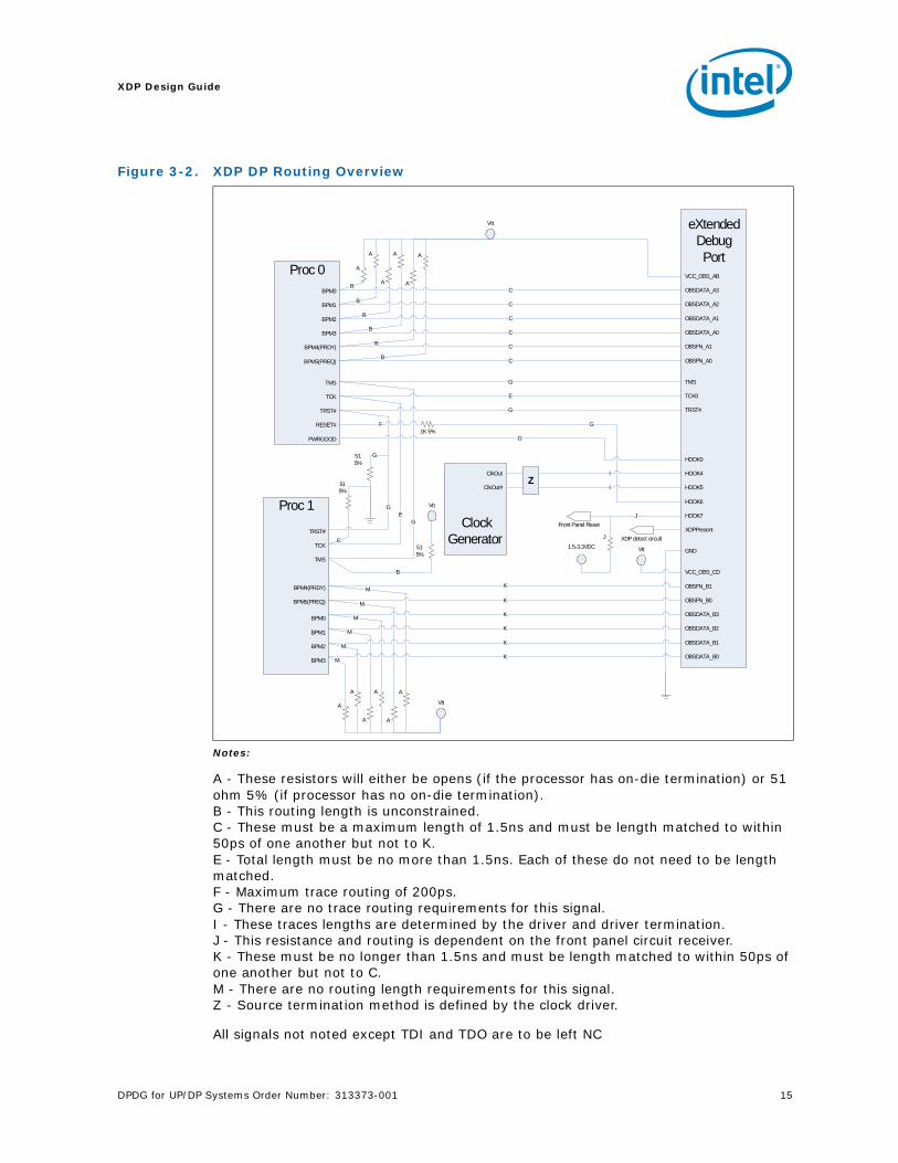
The following diagram illustrates the exterior dimensions of the Run Control hardware as well as board level height restrictions and cable egress. It is recommended that the main tool enclosure be securely attached to the target system to avoid damage to the tool and the target system. Four 1/16” mounting holes are provided to facilitate attachment with screws or cable ties.
The placement of the Samtec* BSH-030-01 debug port connector on the 2nd side should be avoided if possible. Among other reasons, it should be avoided due to the complexity of hand placing and soldering the fine pitch device. Cap all vias near the connector pads in compliance with the Intel DFM Guidelines for capped vias.
DPDG for UP/DP Systems Order Number: 313373-001 25
XDP Design Guide
§
Figure 3-8. XDP Connector System Keepout Diagram

XDP Design Guide
26 DPDG for UP/DP Systems Order Number: 313373-001
DPDG for UP/DP Systems Order Number: 313373-001 27
XDP-SSA Design Guide
4 XDP-SSA Design Guide
4.1 Conventions
Special Note: TDI is an output of the debug port connector and TDO is an input of the debug port connector despite their nomenclature. The opposite is true of a processor. TDI is an input of a processor and TDO is an output.
4.2 XDP-SSA Routing Overview
The XDP-SSA (Second Side Attach) is a 31-pin alternative to the XDP for those customers needing to place the debug port on the non-component side of the board. As there are fewer pins, XDP-SSA has significantly fewer capabilities than XDP
Routing for the XDP-SSA is similar to the XDP. As such, the sections in this chapter will make significant references to Section 3, “XDP Design Guide” on page 13 in this book.
This section contains a thumbnail sketch of how to connect all debug port signals, except TDO/TDI, in the simplest connection configuration. Please refer to the details of each signal for complete information. These drawings represent only the most basic connection.
Note that any signal that is not noted on this drawing may be left as no connect.
4.3 JTAG Routing Guidelines
4.3.1 TDI - TDO Routing Guidelines
The XDP-SSA TDI-TDO routing guidelines are the same as those for the XDP0 TDI-TDO (see Section 3.3.1, “TDI - TDO Routing Guidelines” on page 16).
Special Note: TDI is an output of the debug port connector and TDO is an input of the debug port connector despite their nomenclature. The opposite is true of a processor. TDI is an input of a processor and TDO is an output.
4.3.2 TCK0 Routing
The XDP-SSA TCK0 routing guidelines are the same as those for the XDP0 TCK0 (see Section 3.3.2, “TCK0 Routing” on page 18).
Suggestion: As signal integrity of TCK is one of the primary sources of run control failure, provide a scope test point at ALL device loads (processor, chipset, etc.). This suggestion is typically implemented only on the first spin of a system.
4.3.2.1 TMS Routing Guidelines
The XDP-SSA TMS routing guidelines are the same as those for the XDP0 TMS (see Section 3.3.3, “TMS Routing Guidelines” on page 18).
There is no trace length requirement for this signal.

XDP-SSA Design Guide
28 DPDG for UP/DP Systems Order Number: 313373-001
4.3.3 TRSTn Routing Guidelines
The XDP-SSA TRSTn routing guidelines are the same as those for the XDP0 TRSTn routing guidelines (see Section 3.3.4, “TRSTn Routing Guidelines” on page 18).
There is no trace length requirement for this signal.
4.4 Run Control Routing GuidelinesPlease see Section 3.7.2, “Observation Port Routing” on page 21.
4.5 System Control Routing Guidelines
• System Control operations report or manage the system power, scan, and reset states of the target system. These signals are HOOK[0:7] on the XDP-SSA debug port. HOOK[1:3] are generally left as no-connects.
4.5.1 PWRGOOD (HOOK0) Routing Guidelines
The XDP-SSA PWRGOOD routing guidelines are the same as those for the XDP0 PWRGOOD routing guidelines (see Section 3.5.1, “PWRGOOD (HOOK0) Routing Guidelines” on page 19).
4.5.2 Reserved (HOOK[1:3])
These signals are reserved. No connections to these signals are required.
4.5.3 ITPCLK/ITPCLK# (HOOK[4:5]) Routing Guidelines
The XDP-SSA HOOK[4:5] routing guidelines are the same as those for the XDP0 HOOK[4:5] (see Section 3.5.5, “ITPCLK/ITPCLK# (HOOK[4:5]) Routing Guidelines” on page 19).
4.5.4 RESET_IN# (HOOK6) Routing Guidelines
The XDP-SSA HOOK6 routing guidelines are the same as those for the XDP0 HOOK6 (see Section 3.5.6, “RESET_IN# (HOOK6) Routing Guidelines” on page 20).
4.5.5 RESET_OUT# (HOOK7) Routing Guidelines
The XDP-SSA HOOK7 routing guidelines are the same as those for the XDP0 HOOK7 (see Section 3.5.7, “RESET_OUT# (HOOK7) Routing Guidelines” on page 20).
4.6 I2C* Routing Guidelines
The XDP-SSA I2C* routing guidelines are the same as those for the XDP0 I2C* (see Section 3.6, “I2C* Routing Guidelines” on page 20).
4.7 Observation Port Routing Guidelines
There is a single observation ports on the XDP-SSA labeled A. The observation port is made up of 4 OBSDATA lines and 2 OBSFN control/strobe lines.

DPDG for UP/DP Systems Order Number: 313373-001 29
XDP-SSA Design Guide
These lines in the past have had historical names associated with them. The OBS Port historically has been referred to as the BPM#[0:5] pins.
Terminations on these signals vary based on processor. Check the documentation on the last device on each signal to see if it has on-die termination (ODT). If it does not, the signal requires a 51 ohm pull-ups to VTAP. Note that no termination is needed on the debug port side of the transmission lines.
4.7.1 OBSFN_A[1:0]
The XDP-SSA OBSFN_A[1:0] routing guidelines are the same as those for the XDP0 OBSFN_x[1:0] routing guidelines (see Section 3.7.3, “OBSFN_x[1:0]” on page 21).
4.7.2 OBSDATA_A[3:0]
The XDP-SSA OBSDATA_A[3:0] routing guidelines are the same as those for the XDP0 OBSDATA_A[3:0] routing guidelines (see Section 3.7.4, “OBSDATA_A[3:0]” on page 22).
4.8 Power
4.8.1 VCC_OBS Pins
The VCC_OBS_AB pins are used by the XDP-SSA hardware to provide termination voltage to the OBS interface. The JTAG signals are referenced off of the VCC_OBS pins. Connect VCC_OBS_AB to the VTAP voltage of the processor. Decoupling capacitors are not required for these signals.
This pin draws ~200mA of current.
The XDP-SSA VCC_OBS routing guidelines are the same as those for the XDP0 VCC_OBS (see Section 3.8.1, “VCC_OBS Pins” on page 22).
4.8.2 Ground
All XDP-SSA ground signals must be tied directly to the system ground with little to no trace from the debug port.
4.9 System Connection
The XDP-SSA connector is a Hirose* 31-pin DF9C-31S series connector or equivalent. The following table documents the pinout for this connector.

XDP-SSA Design Guide
30 DPDG for UP/DP Systems Order Number: 313373-001
4.10 Depopulating XDP-SSA for Production Units
At some point there may be a desire to remove the XDP-SSA from production units. It is recommended that the port real-estate and pads remain in place if they need to be populated for a future problem.
Depopulate all physical devices (connector, termination resistors, jumpers) except:
• Termination of OBSFN_x[0:1] / BPM[4:5]# / PREQ#, PRDY#
• Termination of TCK
• Termination of TDI
• Termination of TMS
• Termination of TRSTn
4.11 Mechanical Specifications
The following diagram It is recommended that the main XDP-SSA enclosure be securely attached to the target system to avoid damage to the debug tool and the target system. Four 1/16” mounting holes are provided to facilitate attachment with screws or cable ties.
Table 4-1. XDP-SSA Pinouts
Pin Sig nameTarget Sig
Name I/O Device Pin Sig nameTarget Sig
Name I/O Device
1 OBSFN_A0 BPM[5]# I/O processor1
Notes:
1. To the appropriate processor(s) -- see the description of each signal for more information.
2 GND GND
3 OBSFN_A1 BPM[4]# I/O processor1 4 OBSDATA_A[2] BPM[1]# I/O processor1
5 GND GND 6 OBSDATA_A[3] BPM[0]# I/O processor1
7 OBSDATA_A[0] BPM[3]# I/O processor1 8 GND GND
9 OBSDATA_A[1] BPM[2]# I/O processor1 10 HOOK0 PWRGOOD I
11 GND GND 12 HOOK1 OPEN
13 HOOK4 BCLK[0] I System 14 VCC_OBS_AB Vtt I System
15 HOOK5 BCLK[1] I System 16 HOOK2 OPEN
17 GND GND 18 HOOK3 OPEN
19 HOOK6 RESET# I System 20 GND GND
21 HOOK7 front panel reset2
2. See specific descriptions of these signals for additional information.
O System 22 SCL 1 I/O I2C Device
23 TDO TDO I processor 1 24 SDA 1 I/O I2C Device
25 TRSTn TRSTn O processor1 26 GND GND
27 GND GND 28 TCK1 open O
29 TDI TDI O processor 1 30 TCK0 TCK O processor1
31 TMS TMS O processor1

DPDG for UP/DP Systems Order Number: 313373-001 31
XDP-SSA Design Guide
Cap all vias near the XDP-SSA connector pads in compliance with the Intel DFM Guidelines for capped vias.
Figure 4-1. XDP-SSA Connector System Keepout Diagram

XDP-SSA Design Guide
32 DPDG for UP/DP Systems Order Number: 313373-001
DPDG for UP/DP Systems Order Number: 313373-001 33
ITP700Flex Design Guide
5 ITP700Flex Design Guide
ITP700Flex is a slightly smaller connector than the XDP connector, however it has a much smaller keep-out volume because of the connection methodology (flex edge connector). As such many users prefer this connection method for systems that are extremely tight on physical space such as mobile systems and blade servers.
Intel does not recommend ITP700Flex as there is a loss of capabilities with the use of ITP700Flex and not all tools require the same termination values. These guidelines specify the layout for most systems and notations where there may be discrepancies.
• ITP700Flex allows basic run control at a reduced rate and/or reduced edge rate compared to XDP. The rate is dependent on many different factors that cannot be fully covered here.
• May require the use of an adapter to convert an XDP based run control tool to an ITP700Flex form factor connector.
• ITP700Flex may only be used on a single processor system.
Note: TDI is an output of the debug port connector and TDO is an input of the debug port connector despite their nomenclature. The opposite is true of a processor. TDI is an input of a processor and TDO is an output.
5.1 Conventions
The last device in the scan chain is found by tracing TDO from the XDP connector to TDO of the last device.
5.2 ITP700Flex Routing Overview
This section contains a thumbnail sketch of how to connect all debug port signals in the simplest connection configuration.

ITP700Flex Design Guide
34 DPDG for UP/DP Systems Order Number: 313373-001
Notes:
A - These resistors will either be opens (if the processor has on-die termination) or 51 ohm 5% (if processor has no on-die termination).B - These routings have no routing length constraint.C - All of these routings must be a maximum of 1.5ns. They also must be length matched to within 50ps of one another.D - These traces must be a maximum of 1.5ns. E - These traces have no specific routing requirements. F - These traces lengths are determined the length of the signals from the clock generator to the processor plus the length of the Obs_Data signals.G - Tie VTT and VTAP together and place the ceramic buffering capacitor within 0.1 inches of the ITP700Flex.H - Maximum trace routing of 200ps.I - This resistance and termination voltage is dependent on the front panel circuit receiver.Z - Source termination method is defined by the clock driver.
All signals not noted except TDI and TDO are to be left NC.
Figure 5-1. ITP700Flex Routing Overview
271%
Processor
BPM0
BPM1
BPM2
BPM3
BPM4(PRDY)
BPM5(PREQ)
TDI
TDO
TMS
TCK
TRST#
RESET#
ITP700Flex Debug Port
VTAP
VTT
OBSDATA_A3
OBSDATA_A2
OBSDATA_A1
OBSDATA_A0
OBSFN_A1
OBSFN_A0
TDI
TDO
TMS
TCK
TRST#
FBO
HOOK4
HOOK5
HOOK6
HOOK7
GND
150 5%
391%
Vtt
500-6805%
A
A
A
A
Front Panel Reset
Clock Generator
ClkOut
ClkOut#
E
C
C
C
C
C
C
D
E
H
E
B
B
B
B
E
H
E
F
F
H
E
E
1505%
515%
H
H
c
1.5-3.3VDC
I
E
Z
A
B
0.1uF
G
B
A

DPDG for UP/DP Systems Order Number: 313373-001 35
ITP700Flex Design Guide
5.3 JTAG Routing Guidelines
5.3.1 TDI - TDO Routing Guidelines
Note: TDI is an output of the debug port connector and TDO is an input of the debug port connector despite their nomenclature. The opposite is true of a processor. TDI is an input of a processor and TDO is an output.
There is no trace length requirement for TDI/TDO. TDI termination resistor of 150 ohms 5% must be located at the processor end of the trace. TDO termination resistor of 51 ohms 5% needs to be located at the ITP700Flex debug port end of the trace.
5.3.2 TCK Routing
Route TCK to the processor and terminate with a 27 Ohm, 1% resistor to GND. The trace length for this signal must be a maximum of 1.5ns and must be located within 200ps of ITP700Flex debug port. Any stub on this net must be shorter than 200ps.
Suggestion: As signal integrity of TCK is one of the primary sources of run control failures, provide a scope test point at ALL device loads (processor, debug port, etc.). This suggestion is typically implemented only on the first spin of a system.
5.3.3 TMS Routing Guidelines
Route TMS to the processor on the scan chain and should be terminated with a 39 ohm, 1% resistor to VTAP and must be located within 200ps of ITP700Flex debug port. There is no routing length requirements for this signal from debug port to processor
5.3.4 TRSTn Routing Guidelines
Should be routed to processor with a 500-680 Ohms 5% pull down resistor on the trace. The location of this resistor is recommended to be near the processor with layout described in Section 2.1.1, “Termination Resistors” on page 10 but can be placed in other positions if necessary for platform layout. The total trace length on this signal is unimportant.
5.3.5 FBO
FBO is routed from the processor TCK signal back to the ITP700Flex Debug Port FBO signal with a routing length that must match the lengths of the OBS_Port within 50 ps (see Section 5.5.1, “Observation Port Routing” on page 37).
5.3.6 Run Control Routing Guidelines
Please refer to Section 5.5.1, “Observation Port Routing” on page 37.
5.4 System Control Routing Guidelines
System Control operations report or manage the system power, scan, and reset states of the target system. These signals are HOOK[0:7] with HOOK[0:3] generally left as no-connects.
ITP700Flex Design Guide
36 DPDG for UP/DP Systems Order Number: 313373-001
5.4.1 Reserved (HOOK[0:3])
These signals are reserved. No connections to these signals are required.
5.4.2 ITPCLK/ITPCLK# (HOOK[4:5]) Routing Guidelines
A copy of the processor Front Side Bus Clock (usually BCLK[0:1]) needs to be delivered to the debug port by a system clock component. ITPCLK and ITPCLK# are used for noise and synchronizer fault survivability, and as a frequency reference for run control operations when enabled by the run control tool.
Route differentially from the system clock distribution component to the HOOK[4:5] pins of debug port connector. Provide adequate termination to the clock traces at the clock driver. Some run control and system interaction operations may be disabled if ITPCLK is not connected or unavailable.
The routing length of these signals should be equal to the length of BCLK to the processor plus the length of the Obs_Data lengths.
Due to the variations in processor nomenclature, BCLK[0:1] is sometimes denoted as BCLK[p/n] respectively. Thus, BCLK[0] = BCLK[p] = ITPCLK = HOOK4 is the rising edge for the beginning of every transaction. Conversely, BCLK[1] = BCLK[n] = ITPCLK# = HOOK5.
5.4.3 RESET_IN# (HOOK6) Routing Guidelines
The RESET_IN# signal is an input to the run control tool from front-side bus RESET# signal. Run control tool will not drive RESET#; but uses this signal to sense when a system reset has occurred.
Route RESET# from the processor to the RESET_IN# through a 150 ohm, 5% isolation resistor. Routing of this signal before the isolation resistor is left to the system designers as part of the system design guides. On the debug port side of the isolation resistor, this signal has a length requirement of less than 1ns.
Rather than placing the isolation resistor within 200ps of the processor (as is shown in Routing Overviews), the isolation resistor would ideally be placed to remove any stub from the reset line by placing the isolation resistance pad directly on the RESET# signal line. There is no requirement from the point of view of the run control tool but the system reset wired OR signal will have signal integrity issues with larger than a minimum stub.
Note that not all of the other system RESET routing is noted, only that needed by the ITP700Flex. Consult the appropriate platform design guide for detailed requirements for the processor RESET# signal.
5.4.4 RESET_OUT# (HOOK7) Routing Guidelines
The RESET_OUT# signal is an output from the run control tool to the system reset. The run control tool uses this signal to initiate a system reset. This reset assertion must not cycle any power supplies on the target system nor may it alter the PWRGOOD signal in any way. The run control tool will drive this signal with a silicon switch closure to ground when a debug reset is requested.
Route this signal to any point within the system reset topology that would initiate the appropriate reset. Typical implementations route the RESET_OUT# signal to either a reset controller FPGA; to an OR function within the front panel reset circuit; or directly

DPDG for UP/DP Systems Order Number: 313373-001 37
ITP700Flex Design Guide
into the ICH signal SYS_RESET#. A pull-up resistor must be included on this net of 150 to 240 ohms to the Vtt voltage of the receiver. The resistor should be located near the receiving device.
The RESET_OUT# signal has a legacy name of DBR# (Debug Port Reset).
5.5 Observation Port Routing Guidelines
These lines in the past have had historical names associated with them. For reference: OBSFN0=BPM5=PREQ; OBSFN1=BPM4=PRDY; OBSDATA3=BPM0; OBSDATA2=BPM1; OBSDATA1=BPM2; OBSDATA0=BPM3.
5.5.1 Observation Port Routing
All signals from the single OBS port (OBSDATA[0:3] & OBSFN[0:1]) must be routed to the processor BPM#[0:5]; BPM#[0:3], PREQ#, PRDY#; or OBS port pins. These routings must be length matched to within 50 pS of one another and the longest must not exceed 1.5nS.
Terminations on these signals vary based on processor. Check the documentation on the last device on each signal to see if it has on-die termination (ODT). If it does not, the signal requires a 51 ohm pull-ups to Vtap within 200 pS of that last device. Note that no termination is needed on the debug port side of the transmission lines. No termination is required on signals with ODT.
5.5.2 OBSFN_x[0:1]
Run control operations involve the assertion of signals on processor pins BPM5# and BPM4#.
5.6 Power
5.6.1 VTT, VTAP
VTT and VTAP should be tied together. Within 0.1 inches of the debug port each of these signals should have a 0.1 uF ceramic capacitor. If any of these voltages are the same (as is the case on most processors), tie these ITP700Flex pins together at the debug port and use only a single capacitor for that combined trace.
5.6.2 Ground
All ITP700Flex ground signals must be tied directly to the system ground with little to no trace from the debug port.
5.7 System Connection
The ITP700Flex connector is a 28 pin surface mount device -- Molex* #52435-2872 or equivalent. Specific plating types, versions of this connector can be obtained from Molex*. The following table documents the pinout for this connector.

ITP700Flex Design Guide
38 DPDG for UP/DP Systems Order Number: 313373-001
5.8 XDP Tools to ITP700Flex Adapters
XDP tools require an adapter to mate to the ITP700Flex debug port. Additionally there may be requirements of changing terminations on some signals. Below is a list of termination resistance changes for most XDP based tools. This list is not meant to be all encompassing but rather a guide of items that will need to be changed in all cases. Please contact your vendor of choice for the most recent guidelines for all changes required to use their tool.
• TCK - Change termination resistance to 51 ohm 5%
• RESET_IN# - Isolation resistor change to 1K ohm 5%
• TDI - Change termination resistance to 51 ohms 5%
• TMS - Change termination resistance to 51 ohms 5%
5.9 Mechanical Specifications
The following diagram illustrates the exterior dimensions of the ITP700Flex hardware as well as board level height restrictions and cable egress.
Cap all vias near the ITP700Flex connector pads in compliance with the Intel Design For Manufacturing Guidelines for capped vias.
Table 5-1. ITP700Flex Debug Port Pinout
Pin Sig nameTarget Sig
Name I/O Device Pin Sig nameTarget Sig
Name I/O Device
1 TDI TDI O processor 2 TMS TMS O processor
3 TRST# TRST# O processor 4 No Connect OPEN
5 TCK0 TCK O processor 6 No Connect OPEN
7 TDO TDO I processor 8 HOOK5 BCLKn1 I system
9 HOOK4 BCLKp I Clock Generator
10 GND GND
11 FBO TCK1 I processor1 12 HOOK6 RESET# I system
13 OBSFN_A0 BPM[5]# I/O processor 14 GND GND
15 OBSFN_A1 BPM[4]# I/O processor 16 GND GND
17 OBSDATA_A[0] BPM[3]# I/O processor 18 GND GND
19 OBSDATA_A[1] BPM[2]# I/O processor 20 GND GND
21 OBSDATA_A[2] BPM[1]# I/O processor 22 GND GND
23 OBSDATA_A[3] BPM[0]# I/O processor 24 NC
25 HOOK7 Front panel reset1
O system 26 VTAP Vtt of scan chain
27 Vtt Vtt 28 Vtt Vtt
Notes:1. See specific descriptions of these signals for additional information2. To the appropriate processor -- see the description of each signal for more information.
DPDG for UP/DP Systems Order Number: 313373-001 39
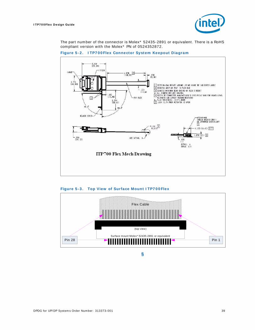
ITP700Flex Design Guide
The part number of the connector is Molex* 52435-2891 or equivalent. There is a RoHS compliant version with the Molex* PN of 0524352872.
§
Figure 5-2. ITP700Flex Connector System Keepout Diagram
Figure 5-3. Top View of Surface Mount ITP700Flex
Flex Cable
(top view)
Surface mount Molex* 52435-2891 or equivalent
Pin 1Pin 28

ITP700Flex Design Guide
40 DPDG for UP/DP Systems Order Number: 313373-001
DPDG for UP/DP Systems Order Number: 313373-001 41
Appendix A – Debug Port Interposer Considerations
A Appendix A – Debug Port Interposer Considerations
UP systems may be routed to support interposer-based run control tool debug ports. The following pins need to be connected correctly in order for interposer-based debug ports to function.
1. The DBR# pin of the processor must be connected to the same reset circuit as HOOK7. In fact, as both will not be driven at the same time, connect them directly together.
2. The ITPCLK and ITPCLK# pins of the processor must be provided a copy of BCLK[0:1] from the system clock distribution component. It is acceptable to use resistor stuffing on the motherboard to route a clock output from the clock distribution component to the processor when an on-board debug port is not populated, and route that same clock output to the on-board debug port instead if the on-board debug port is populated.
§

Appendix A – Debug Port Interposer Considerations
42 DPDG for UP/DP Systems Order Number: 313373-001