
Dear customer - LAPIS Technology LSI
22
Dear customer LAPIS Semiconductor Co., Ltd. ("LAPIS Semiconductor"), on the 1 st day of October, 2020, implemented the incorporation-type company split (shinsetsu-bunkatsu) in which LAPIS established a new company, LAPIS Technology Co., Ltd. (“LAPIS Technology”) and LAPIS Technology succeeded LAPIS Semiconductor’s LSI business. Therefore, all references to "LAPIS Semiconductor Co., Ltd.", "LAPIS Semiconductor" and/or "LAPIS" in this document shall be replaced with "LAPIS Technology Co., Ltd." Furthermore, there are no changes to the documents relating to our products other than the company name, the company trademark, logo, etc. Thank you for your understanding. LAPIS Technology Co., Ltd. October 1, 2020
Transcript of Dear customer - LAPIS Technology LSI

Dear customer LAPIS Semiconductor Co., Ltd. ("LAPIS Semiconductor"), on the 1st day of October, 2020, implemented the incorporation-type company split (shinsetsu-bunkatsu) in which LAPIS established a new company, LAPIS Technology Co., Ltd. (“LAPIS Technology”) and LAPIS Technology succeeded LAPIS Semiconductor’s LSI business. Therefore, all references to "LAPIS Semiconductor Co., Ltd.", "LAPIS Semiconductor" and/or "LAPIS" in this document shall be replaced with "LAPIS Technology Co., Ltd." Furthermore, there are no changes to the documents relating to our products other than the company name, the company trademark, logo, etc. Thank you for your understanding.
LAPIS Technology Co., Ltd. October 1, 2020

MR1M Bit(
GENER The MR4in the fePeripherato hold dthose usepower coThe MR4tolerance
FEATUR • 131,072• A singl• Operati• Read/w• Data ret• Guarant• Low po
Power StandbSleep m
• Package
8-p8-p
• RoHS (
R45V1(131,072-Wor
RAL DESCR
45V100A is aerroelectric pral Interface. Udata. This deved for variousonsumption du45V100A can of 1012 cycle
RES
2-word × 8-bite 1.8V to 3.6Ving frequency
write tolerance tention teed operating
ower consumpsupply curren
by mode supplmode supply c
e options: pin plastic SOpin plastic DIP(Restriction of
100A rd × 8-Bit) FeR
RIPTION
a nonvolatile 1rocess and sil
Unlike SRAMsvice has no ms EEPROMs. uring a write c
be used in vas per bit and t
t configuratioV (3.3V typ.):
g temperature ption nt (@40MHz)ly current current
OP (P-SOP8-2P (P-DIP8-30f hazardous su
RAM (Ferroel
128Kword x 8licon-gate CMs, this device,
mechanisms ofTherefore, th
can be reducedarious applicatthe rewrite cou
n (Serial Perip) power supp
range
00-1.27-T2K)0-2.54-T6)
ubstances) com
lectric Random
8-bit ferroelecMOS technolo
whose cells af erasing and e write cycle d significantlytions, becauseunt can be ext
pheral Interfaply
34MHz(R1012 cycle10 years−40 to 85
3.0mA(T10μA(Ty0.1μA(Ty
)
mpliant
m Access Mem
ctric random aogy. The MRare nonvolatile
programmingtime can be
y. e the device is tended signific
ce: SPI)
READ cycle) es/bit
5°C
Typ.), 4.yp.), 50yp.), 2μ
Iss
mory) SPI
access memorR45V100A is e, eliminates bg memory celequal to the r
guaranteed focantly.
/ 40MHz(Exc
5mA(Max.) 0μA(Max.) μA(Max.)
FEDR45Vsue Date: Sep
ry (FeRAM) s accessed usbattery backup
ells and blockread cycle tim
or the write/re
cept for READ
V100A-01. 4, 2017
1/21
developed ing Serial p required
ks, such as me and the
ead
D)

FEDR45V100A-01
MR45V100A
2/21
PIN CONFIGURATION (Top View)
Note: Signal names that end with # indicate that the signals are negative-true logic.
PIN DESCRIPTIONS
Pin Name Description
CS# Chip Select (input, negative logic)
Latches an address by low input, activates the FeRAM, and enables read or write operation. High input goes the device disable state.
WP# Write Protect( input, negative logic )
Write Protect pin controls write-operation to the status-register(BP0,BP1). This pin should be fixed low or high in write-operations.
HOLD#
HOLD( input, negative logic )
Hold pin is used when the serial-communication suspended without disable the chip select. When HOLD# is low, the serial-output is in High-Z status and serial-input/serial-clock are “Don’t Care”. CS# should be low in hold operation.
SCK Serial Clock
Serial Clock is the clock input pin for setting for serial data timing. Inputs are latched on the rising edge and outputs occur on the falling edge.
SI Serial input
SI pins are serial input pins for Operation-code, addresses, and data-inputs.
SO Serial output
SO pins are serial output pins.
VCC, VSS Power supply
Apply the specified voltage to VCC. Connect VSS to ground.
8-pin plastic SOP / DIP
CS# SO WP# VSS
VCC HOLD# SCK SI
1 8 2 7 3 6 4 5
MR
45V100A

FEDR45V100A-01
MR45V100A
3/21
SPI MODE (Serial Peripheral Interface)
SPI mode0(CPOL=0, CPHA=0)
SPI mode3(CPOL=1, CPHA=1)
STATUS REGISTER
Name Function
WIP Fixed to 0.
WEL Write Enable Latch. This indicates internal WEL condition.
BP0,BP1 Block Protect: These bits can change protected area. This is the software protect.
SRWD Status Register Write Disable(SRWD): SRWD controls the effect of the hardware WP# pin. This device will be in hardware-protect by combination of SRWD and WP#.
0 Fixed to 0.
SRWD 0 0 0 BP1 BP0 WEL WIP
b7 b0
Status Register Write Disable
Block Protect Bits
Write Enable Latch
Write In Progress (Always 0)
CS#
SCK
SI LSB MSB
CS#
SCK
SI LSB MSB

FEDR45V100A-01
MR45V100A
4/21
OPERATION-CODE Operation codes are listed in the table below. If the device receives invalid operation code, the device will be deselected.
Instruction Description Instruction format
WREN Write Enable 0000 0110
WRDI Write Disable 0000 0100
RDSR Read Status Register 0000 0101
WRSR Write Status Register 0000 0001
READ Read from Memory Array 0000 0011
WRITE Write to Memory Array 0000 0010
FSTRD Fast Read from Memory Array 0000 1011
RDID Read device ID 1001 1111
SLEEP Enter Sleep Mode 1011 1001

FEDR45V100A-01
MR45V100A
5/21
COMMANDS
WREN (Write Enable)
It is necessary to set Write Enable Latch(WEL)bit before write-operation (WRITE and WRSR).
WREN command sets WEL bit.
WRDI (Write Disable) WRDI command resets WEL bit.
CS#
SCK
SI
WP# Fixed “H” 0 1 2 3 4 5 6 7
SOHigh-Z
CS#
SCK
SI
WP# Fixed “H”
0 1 2 3 4 5 6 7
SOHigh-Z

FEDR45V100A-01
MR45V100A
6/21
RDSR (READ Status Register) The RDSR command allows reading data of status register. The Status Register can be read anytime and any number of times.
WRSR (WRITE Status Register)
WRSR command allows to write data to status register(SRWD,BP0,BP1). It is necessary to set Write Enable Latch(WEL)bit by WREN command before executing WRSR. WRSR command cannot write RFU(b6,b5,b4), WEL(b1), WIP(b0) of Status Resistor..
CS#
SCK
SI
WP# Fixed “H”
0
SOHigh-Z
1 2 3 4 5 6 7 8 9 10 11 12 13 14 15
SRWD BP1 BP0 WEL WIP SRWD0 0 0
7 6 5 4 3 2 1 0 7
CS#
SCK
SI
0
SOHigh-Z
1 2 3 4 5 6 7 8 9 10 11 12 13 14 15
BP0 X X
7 6 5 4 3 2 1 0
BP1 XXXSRWD
Note: WP#=Fixed ”H”

FEDR45V100A-01
MR45V100A
7/21
READ (Read from Memory Array) READ command can be valid when CS# goes “L”, then the op-code and 24bit-addresses are inputted to serial input ”SI”. The inputted addresses are loaded to internal register, then the data from corresponded address is outputted at serial-output “SO”. If CS# will keep “L”, the internal address will be increased automatically after 8 clocks and will output the data from new-address. When it reaches the most significant address, the address counter rolls over to starting address, and reading cycle can be continued infinitely. To finish read cycle, make the CS# “H” during LSB output clock.
FSTRD (Fast Read from Memory Array) FSTRD command can be valid when CS# goes “L”, then the op-code and 24bit-addresses are inputted to serial input ”SI”. After 8bits for dummy byte, the data from corresponded address is outputted at serial-output “SO”. If CS# will keep “L”, the internal address will be increased automatically after 8 clocks and will output the data from new-address. When it reaches the most significant address, the address counter rolls over to starting address, and reading cycle can be continued infinitely. To finish read cycle, make the CS# “H” during LSB output clock.
CS#
SCK
SI
0
SO High-Z
1 2 3 4 5 6 7 8 9 15 16 28 29 30 31
A2 A1 A0
23 22 16 3 2 1 0
A3 A16XX
24bit Address (An)
15
A15
CS#
SCK
SI
32
SO
33 34 35 36 37 38 39 40 41 42 43 46 47 m
Data Out (An)
Q7 Q6 Q5 Q4 Q3 Q2 Q1 Q0 Q7 Q6 Q5 Q4 Q3 Q2 Q1 Q0
Data Out (An+1)
Q0
44 45
Note : WP# = fixed ”H”
14
17
X
m-1
Q1 Q2
m-2
CS#
SCK
SI
SO High-Z
CS#
SCK
SI
32
SO
33 34 35 36 37 38 39 40 41 42 43 46 47 m
Dummy Byte
Q7 Q6 Q5 Q4 Q3 Q2 Q1 Q0
Data Out (An)
Q0
44 45
Note : WP# = fixed ”H”
Q1
0 1 2 3 4 5 6 7 8 9 15 16 28 29 30 31
A2 A1 A0
23 22 16 3 2 1 0
A3 A16XX
24bit Address (An)
15
A15
14
17
X
m-1
FEDR45V100A-01
MR45V100A
8/21
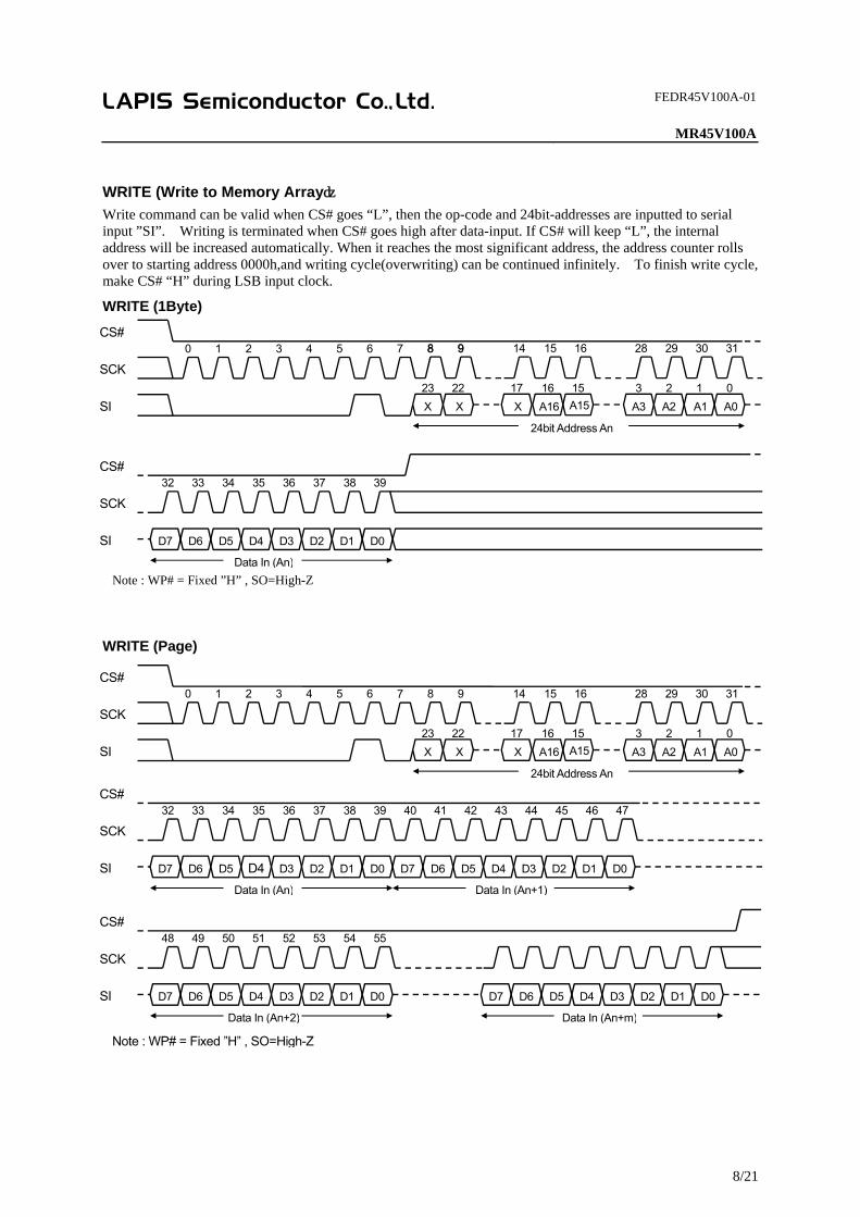
WRITE (Write to Memory Array)
Write command can be valid when CS# goes “L”, then the op-code and 24bit-addresses are inputted to serial input ”SI”. Writing is terminated when CS# goes high after data-input. If CS# will keep “L”, the internal address will be increased automatically. When it reaches the most significant address, the address counter rolls over to starting address 0000h,and writing cycle(overwriting) can be continued infinitely. To finish write cycle, make CS# “H” during LSB input clock.
WRITE (1Byte)
WRITE (Page)
CS#
SCK
SI
0 1 2 3 4 5 6
CS#
SCK
SI
Note : WP# = Fixed ”H” , SO=High-Z
32 33 34 35 36 37 38 39 40 41 42 43 46 47
Data In (An)
D7 D6 D5 D4 D3 D2 D1 D0 D7 D6 D5 D4 D3 D2 D1 D0
Data In (An+1)
44 45
CS#
SCK
SI
48 49 50 51 52 53 54 55
Data In (An+2)
D7 D6 D5 D4 D3 D2 D1 D0 D7 D6 D5 D4 D3 D2 D1 D0
Data In (An+m)
8 9 15 16 28 29 30 31
A2 A1 A0
23 22 16 3 2 1 0
A3 A16XX
15
A15
14
17
X
7
24bit Address An
8 9 15 16 28 29 30 31
A2 A1 A0
23 22 16 3 2 1 0
A3 A16XX
15
A15
14
17
X
CS#
SCK
SI
0 1 2 3 4 5 6 7 8 9
24bit Address An
CS#
SCK
SI
Note : WP# = Fixed ”H” , SO=High-Z
32 33 34 35 36 37 38 39
Data In (An)
D7 D6 D5 D4 D3 D2 D1 D0

FEDR45V100A-01
MR45V100A
9/21
WRITE PROTECTION
Writing protection block is shown as follows: When Status Resister Write Disable(SRWD) bit is reset to “0”, Status Resister number can be changed
Protect Block size
Block Protect BIT Protected Block Protected Address Area
BP1 BP0
0 0 None None
0 1 Upper 1/4 block 18000h – 1FFFFh
1 0 Upper 1/2 block 10000h – 1FFFFh
1 1 All 00000h – 1FFFFh
Writing Protect
WP# SRWD mode Writing protection status
in status register
Protection status in memory
Protected blocks Unprotected
blocks
1 0
Software protection (SPM)
Status register is unprotected when WEL-bit is set by WREN command. BP0 and BP1 are unprotected.
Protected Unprotected 0 0
1 1
0 1 Hardware protection (HPM)
Status register is protected. BP0 and BP1 are protected.
Protected Unprotected
FEDR45V100A-01
MR45V100A
10/21
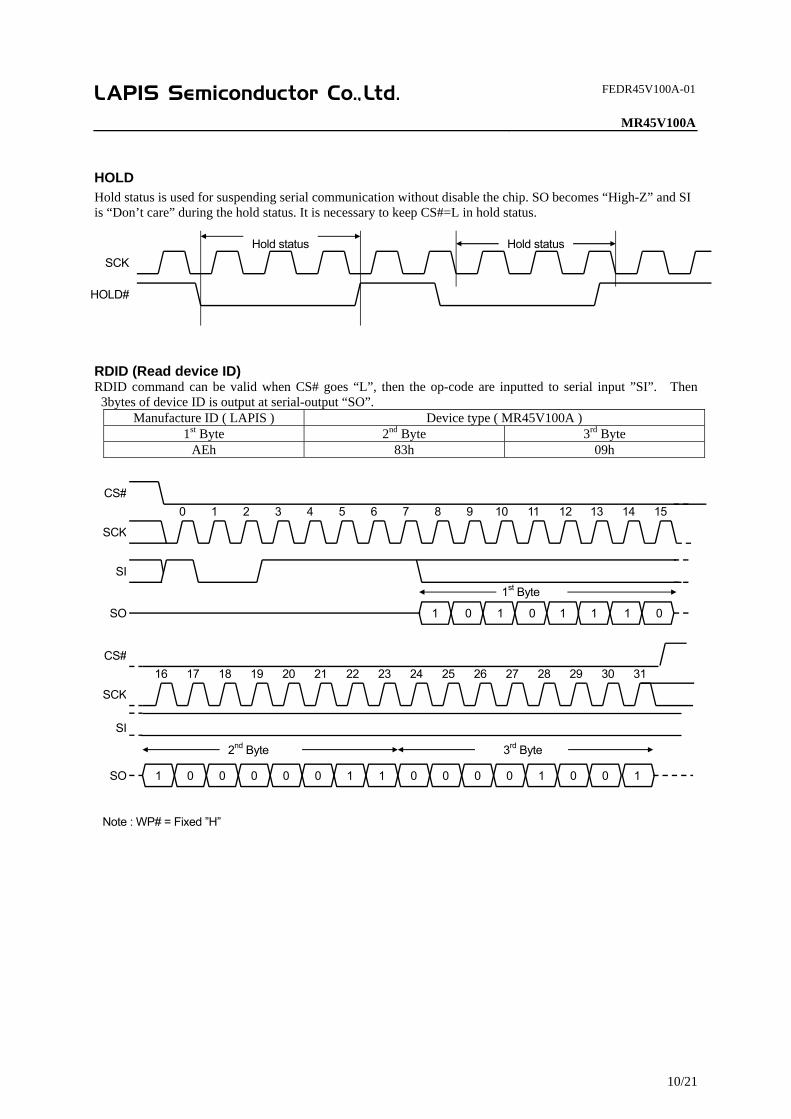
HOLD Hold status is used for suspending serial communication without disable the chip. SO becomes “High-Z” and SI is “Don’t care” during the hold status. It is necessary to keep CS#=L in hold status.
RDID (Read device ID) RDID command can be valid when CS# goes “L”, then the op-code are inputted to serial input ”SI”. Then 3bytes of device ID is output at serial-output “SO”.
Manufacture ID ( LAPIS ) Device type ( MR45V100A ) 1st Byte 2nd Byte 3rd Byte
AEh 83h 09h
HOLD#
SCK
Hold status Hold status
CS#
SCK
SI
0 1 2 3 4 5 6 7 8 9 10 11 12 13 14 15
1st Byte
CS#
SCK
SO
Note : WP# = Fixed ”H”
16 17 18 19 20 21 22 23 24 25 26 27 30 31
2nd Byte
1 0 0 0 0 0 1 1 0 0 0 0 1 0 0 1
3rd Byte
28 29
SO 1 1 01 101 0
SI

FEDR45V100A-01
MR45V100A
11/21
SLEEP
SLEEP command transits MR45V100A to SLEEP Mode, and becomes low current consumption status.
Enter Sleep Mode
(1) Send SLEEP command “B9h”.
(2) MR45V100A starts transition to SLEEP mode after rising edge of CS#.
After the command is determined at 7th clock of SCK, SCK and SI input becomes “Don’t care” and transit to SLEEP mode at the rising edge of CS#.
While CS# keeping “High” level, MR45V100A maintains SLEEP mode.
Exit Sleep Mode
(1) When CS# falling to Low level, MR45V100A start returning SLEEP Mode.
(2) When the time of tREC being after CS# falling, the return operation from SLEEP mode is finished and command can be input.
And, before the time of tREC, the confirmation of returning is possible by doing dummy read.
0 1 2 3 4 5 6 7
CS#
SCK
SI
SO Hi
1 0 1 1 1 0 0 1
↑Enter SLEEPMode
↑Start of returnfrom SLEEP
0 1 2 3 4
↑Exit SLEEPMode
tREC
VALID
tSHSL_SL

FEDR45V100A-01
MR45V100A
12/21
ELECTRICAL CHARACTERISTICS
ABSOLUTE MAXIMUM RATINGS The application of stress (voltage, current, or temperature) that exceeds the absolute maximum rating may damage the device. Therefore, do not allow actual characteristics to exceed any one parameter ratings
PIN VOLTAGES
Parameter Symbol Rating
Unit Min. Max.
Pin Voltage (Input Signal) VIN –0.5 VCC + 0.5 V
Pin Voltage (Input/Output Voltage) VINQ, VOUTQ –0.5 VCC + 0.5 V
Power Supply Voltage VCC –0.5 4.0 V
TEMPERATURE RANGE
Parameter Symbol Rating
Unit Note Min. Max.
Storage Temperature Tstg –55 125 °C
Operating Temperature Topr –40 85 °C
OTHERS
Parameter Symbol Rating Note
Power Dissipation PD 1,000mW Ta=25°C

FEDR45V100A-01
MR45V100A
13/21
RECOMMENDED OPERATING CONDITIONS
POWER SUPPLY VOLTAGE
Parameter Symbol Min. Typ. Max. Unit
Power Supply Voltage VCC 1.8 3.3 3.6 V
Ground Voltage VSS 0 0 0 V
DC INPUT VOLTAGE
Parameter Symbol Min. Max. Unit
Input High Voltage VIH VCC x 0.7 VCC+0.3 V
Input Low Voltage VIL –0.3 VCC x 0.3 V
OVERSHOOT/UNDERSHOOT TOLERANCE (Input signal)
Parameter Symbol Pulse Width Peak
“H” input VIH OVERSHOOT ≤ 20ns VCC+1.0V
“L” input VIL UNDERSHOOT ≤ 20ns – 1.0V

FEDR45V100A-01
MR45V100A
14/21
DC CHARACTERISTICS
DC INPUT/OUTPUT CHARACTERISTICS
Parameter Symbol Condition Min. Max. Unit Note
Output High Voltage VOH IOH =–2mA VCC×0.85 ― V
Output Low Voltage VOL IOL =2mA ― VCC×0.15 V
Input Leakage Current ILI ― –10 10 µA
Output Leakage Current
ILO ― –10 10 µA
POWER SUPPLY CURRENT VCC=Max.to Min, Ta=Topr
Parameter Symbol Condition Min. Typ. Max. Unit Note
Power Supply Current (Standby)
ICCS CS#= VCC,
Other input terminals: VIN=0V or VCC
― 10 50 µA 1
Power Supply Current (Sleep)
IZZ CS#=VCC, Other input terminals :
VIN=0V or VCC ― 0.1 2 µA 1
Power Supply Current (Operating)
ICCA SCK=40MHz, IOUT=0mA ― 3 4.5 mA 1
Note: 1. Average electric current.

FEDR45V100A-01
MR45V100A
15/21
AC CHARACTERISTICS SPI mode AC characteristics
VCC=Max. to Min., Ta=Topr.
Parameter Symbol Read Cycle Except for READ
Unit Note Min. Max. Min. Max.
Clock frequency fC D.C. 34 D.C. 40 MHz
CS# setup time tSLCH 10 ― 10 ― ns
CS# De-select time tSHSL 10 ― 10 ― ns
CS# De-select time (SLEEP)
tSHSL_SL 300 ― 300 ― ns
CS# active hold time tCHSH 10 ― 10 ― ns
SCK High time tCH 13 ― 11 ― ns 1
SCK Low time tCL 13 ― 11 ― ns 1
Data Setup time tDVCH 5 ― 5 ― ns
Data Hold time tCHDX 5 ― 5 ― ns
SCK Low Hold time after HOLD# inactive
tHHCH 10 ― 10 ― ns
SCK Low Hold time after HOLD# active
tHLCH 10 ― 10 ― ns
SCK High Setup time before HOLD# active
tCHHL 10 ― 10 ― ns
SCK High Setup time before HOLD# inactive
tCHHH 10 ― 10 ― ns
Output disable time tSHQZ ― 12 ― 12 ns 2
SCK Low to Output Valid time
tCLQV ― 12 ― 9 ns VCC≧2.7V
― 13 ― 10 ns VCC<2.7V
Output Hold time tCLQX 0 ― 0 ― ns
Input rise time tRI ― 50 ― 50 ns 2
Inputt fall time tFI ― 50 ― 50 ns 2
HOLD# High to Output Low impedance time
tHHQX ― 20 ― 20 ns 2
HOLD# High to Output High impedance time
tHLQZ ― 20 ― 20 ns 2
Recovery time from SLEEP mode
tREC ― 100 ― 100 µs
Note: 1. tCH+tCL≧1/fC
2. sample value

FEDR45V100A-01
MR45V100A
16/21
TIMING DIAGRAMS
SERIAL INPUT TIMING
HOLD TIMING
OUTPUT TIMING
CS#
SCK
SO
SI
HOLD#
tCHHL tHLCH tHHCH
tHHQX
tCHHH
tHLQZ
tQLQHtQHQL
CS#
SCK
SO
SI
Address, LSB IN
tCH
tCL
tSHQZ
tCLQV
tCLQX tCLQX
tCLQV
LSB OUT
tRI
tFI
CS#
tCHSH
SCK
SI
SO
MSB IN LSB IN
High Impedance
tSLCH
tDVCH tCHDX
tSLCH tCHSH
tSHSL

FEDR45V100A-01
MR45V100A
17/21
POWER-ON and POWER-OFF CHARACTERISTICS (Under recommended operating conditions)
Parameter Symbol Min. Max. Unit Note Power-On CS# High Hold Time tVHEL 100 ⎯ ns 1, 2 Power-Off CS# High Hold Time tEHVL 0 ⎯ ns 1 Power-On Interval Time tVLVH 0 ⎯ μs 2 Power-On time tR 30 ⎯ μs/V Power-Off time tF 30 ⎯ μs/V
Notes: 1. To prevent an erroneous operation, be sure to maintain CS#="H", and set the FeRAM in an inactive state
(standby mode) before and after power-on and power-off. 2. Powering on at the intermediate voltage level will cause an erroneous operation; thus, be sure to power up
from 0 V. 3. Enter all signals at the same time as power-on or enter all signals after power-on.
Power-On and Power-Off Sequences
0V
VIL Max.
VCC Min.
VCC
VIH Min.
CS#0V
VIL Max.
VCC Min.
VCC
VIH Min.
CS#
tVHEL
tVLVH
tEHVL
tR tF
FEDR45V100A-01
MR45V100A
18/21
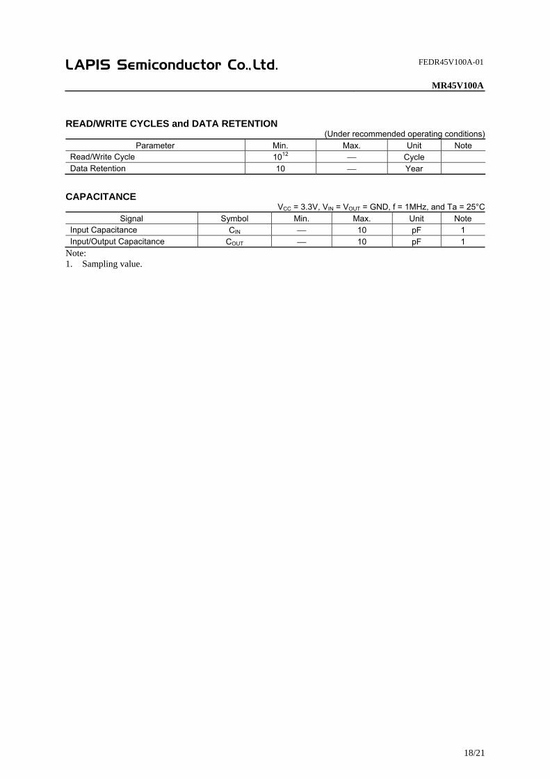
READ/WRITE CYCLES and DATA RETENTION (Under recommended operating conditions)
Parameter Min. Max. Unit Note Read/Write Cycle 1012 ⎯ Cycle Data Retention 10 ⎯ Year
CAPACITANCE VCC = 3.3V, VIN = VOUT = GND, f = 1MHz, and Ta = 25°C
Signal Symbol Min. Max. Unit Note Input Capacitance CIN ⎯ 10 pF 1 Input/Output Capacitance COUT ⎯ 10 pF 1
Note: 1. Sampling value.

PACKA
8-
8-p
Notes fo The surfastorage. Tpackage times).
AGE DIMENS
-pin plastic D
pin plastic S
or Mounting
ace mount typTherefore, bename, pin nu
SIONS
DIP
SOP
g the Surface
pe packages fore you perf
umber, packag
e Mount Typ
are very suscform reflow mge code and d
pe Package
ceptible to hemounting, condesired moun
at in reflow mntact a ROHMnting condition
mounting andM sales officens (reflow me
(Unit: mm
FEDR45
MR
d humidity abe for the prodethod, temper
m)
5V100A-01
R45V100A
19/21
bsorbed in duct name, rature and

FEDR45V100A-01
MR45V100A
20/21
Revision History
Document No. Date Page
Description PreviousEdition
Current Edition
FEDR45V100A-01 Sep. 04, 2017 – – Final edition 1

FEDR45V100A-01
MR45V100A
21/21
Notes 1) The information contained herein is subject to change without notice. 2) Although LAPIS Semiconductor is continuously working to improve product reliability and quality,
semiconductors can break down and malfunction due to various factors. Therefore, in order to prevent personal injury or fire arising from failure, please take safety measures such as complying with the derating characteristics, implementing redundant and fire prevention designs, and utilizing backups and fail-safe procedures. LAPIS Semiconductor shall have no responsibility for any damages arising out of the use of our Products beyond the rating specified by LAPIS Semiconductor.
3) Examples of application circuits, circuit constants and any other information contained herein are provided only to illustrate the standard usage and operations of the Products. The peripheral conditions must be taken into account when designing circuits for mass production.
4) The technical information specified herein is intended only to show the typical functions of the Products and examples of application circuits for the Products. No license, expressly or implied, is granted hereby under any intellectual property rights or other rights of LAPIS Semiconductor or any third party with respect to the information contained in this document; therefore LAPIS Semiconductor shall have no responsibility whatsoever for any dispute, concerning such rights owned by third parties, arising out of the use of such technical information.
5) The Products are intended for use in general electronic equipment (i.e. AV/OA devices, communication, consumer systems, gaming/entertainment sets) as well as the applications indicated in this document.
6) The Products specified in this document are not designed to be radiation tolerant. 7) For use of our Products in applications requiring a high degree of reliability (as exemplified below), please
contact and consult with a LAPIS Semiconductor representative: transportation equipment (i.e. cars, ships, trains), primary communication equipment, traffic lights, fire/crime prevention, safety equipment, medical systems, servers, solar cells, and power transmission systems.
8) Do not use our Products in applications requiring extremely high reliability, such as aerospace equipment, nuclear power control systems, and submarine repeaters.
9) LAPIS Semiconductor shall have no responsibility for any damages or injury arising from non-compliance with the recommended usage conditions and specifications contained herein.
10) LAPIS Semiconductor has used reasonable care to ensure the accuracy of the information contained in this document. However, LAPIS Semiconductor does not warrant that such information is error-free and LAPIS Semiconductor shall have no responsibility for any damages arising from any inaccuracy or misprint of such information.
11) Please use the Products in accordance with any applicable environmental laws and regulations, such as the RoHS Directive. For more details, including RoHS compatibility, please contact a ROHM sales office. LAPIS Semiconductor shall have no responsibility for any damages or losses resulting non-compliance with any applicable laws or regulations.
12) When providing our Products and technologies contained in this document to other countries, you must abide by the procedures and provisions stipulated in all applicable export laws and regulations, including without limitation the US Export Administration Regulations and the Foreign Exchange and Foreign Trade Act.
13) This document, in part or in whole, may not be reprinted or reproduced without prior consent of LAPIS Semiconductor.
Copyright 2017 LAPIS Semiconductor Co., Ltd.
2-4-8 Shinyokohama, Kouhoku-ku,
Yokohama 222-8575, Japan http://www.lapis-semi.com/en/