DDR Timing Wizard User Guide - intel.com · Altera Corporation 1–3 November 2007 DDR Timing...
92
101 Innovation Drive San Jose, CA 95134 http://www.altera.com DDR Timing Wizard UG-DDRTMNG-3.0 Document Version: 3.0 Document Date: November 2007 User Guide
Transcript of DDR Timing Wizard User Guide - intel.com · Altera Corporation 1–3 November 2007 DDR Timing...

101 Innovation DriveSan Jose, CA 95134http://www.altera.com
DDR Timing Wizard
UG-DDRTMNG-3.0
Document Version: 3.0Document Date: November 2007
User Guide
ii Altera Corporation
101 Innovation DriveSan Jose, CA 95134www.altera.comTechnical Support:www.altera.com/support/Literature Services:[email protected]
Copyright © 2007 Altera Corporation. All rights reserved. Altera, The Programmable Solutions Company,the stylized Altera logo, specific device designations, and all other words and logos that are identified astrademarks and/or service marks are, unless noted otherwise, the trademarks and service marks of AlteraCorporation in the U.S. and other countries. All other product or service names are the property of their re-spective holders. Altera products are protected under numerous U.S. and foreign patents and pendingapplications, maskwork rights, and copyrights. Altera warrants performance of its semiconductor productsto current specifications in accordance with Altera's standard warranty, but reserves the right to make chang-es to any products and services at any time without notice. Altera assumes no responsibility or liabilityarising out of the application or use of any information, product, or service describedherein except as expressly agreed to in writing by Altera Corporation. Altera customersare advised to obtain the latest version of device specifications before relying on any pub-lished information and before placing orders for products or services.
Altera Corporation November 2007
Table of Contents
About this User Guide .............................................................................. vRevision History .................................................................................................................................... 1–vHow to Contact Altera .......................................................................................................................... 1–vTypographic Conventions .................................................................................................................. 1–vi
Chapter 1. About the DDR Timing WizardRelease Information ............................................................................................................................... 1–1Device Family Support ......................................................................................................................... 1–2Introduction ............................................................................................................................................ 1–2
Background ....................................................................................................................................... 1–2DDR Timing Wizard ........................................................................................................................ 1–3
Features ................................................................................................................................................... 1–6
Chapter 2. Getting StartedSystem and Software Requirements ................................................................................................... 2–1Design Flow ............................................................................................................................................ 2–1Launching the DDR Timing Wizard ................................................................................................... 2–5Entering and Editing Inputs to the DTW ........................................................................................... 2–6
Import Flow for the Altera Legacy Memory Controller IP Core or Recommended Data Path.............................................................................................................................................................. 2–7Manual Flow for Other External Memory Interfaces or Source Synchronous Systems ...... 2–14
The DTW Pages for DDR/DDR2 SDRAM ............................................................................ 2–14The DTW Pages for QDRII+/QDRII SRAM & RLDRAM II ............................................... 2–45
DTW Limitations ................................................................................................................................. 2–46
Chapter 3. Using the dtw_timing_analysis.tcl ScriptIntroduction ............................................................................................................................................ 3–1
Running dtw_timing_analysis.tcl Script ....................................................................................... 3–3The dtw_timing_analysis.tcl Script Results .................................................................................. 3–6
Timing Closure Process ...................................................................................................................... 3–12Timing Closure Differences in DDR2/DDR SDRAM, QDRII+/QDRII SRAM, and RLDRAM II Interfaces .......................................................................................................................................... 3–14
DDR2/DDR SDRAM Interfaces ............................................................................................. 3–14QDRII+/QDRII SRAM Interfaces ........................................................................................... 3–14RLDRAM II Interfaces .............................................................................................................. 3–15
Selecting Initial Phase Shifts ......................................................................................................... 3–16Re-run DTW After First Compile When Using Classic Timing Analyzer ............................. 3–18Ensure the Changes Made Outside Legacy Controller MegaWizard Are Not Erased When the Core is Regenerated ....................................................................................................................... 3–19Decide When to Change Clock Phase Shift ................................................................................ 3–21
iii

Table of Contents DDR Timing Wizard User Guide
Changing Clock Phase Shift .......................................................................................................... 3–23Adjusting Clock Cycle Selections ................................................................................................. 3–25Changing Clock Cycles .................................................................................................................. 3–27Changing the Address/Command Clock Connection and Phase Shift ................................. 3–28Moving the Data Path Registers Closer to the Pins ................................................................... 3–30
Conclusion ............................................................................................................................................ 3–32
iv Altera CorporationNovember 2007
Altera Corporation November 2007
About this User Guide
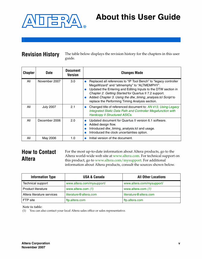
Revision History The table below displays the revision history for the chapters in this user guide.
How to Contact Altera
For the most up-to-date information about Altera products, go to the Altera world-wide web site at www.altera.com. For technical support on this product, go to www.altera.com/mysupport. For additional information about Altera products, consult the sources shown below.
Chapter Date Document Version Changes Made
All November 2007 3.0 ● Replaced all references to “IP Tool Bench” to “legacy controller MegaWizard” and “altmemphy” to “ALTMEMPHY”.
● Updated the Entering and Editing Inputs to the DTW section in Chapter 2. Getting Started for Quartus II 7.2 support.
● Added Chapter 3. Using the dtw_timing_analysis.tcl Script to replace the Performing Timing Analysis section.
All July 2007 2.1 ● Changed title of referenced document to: AN 413, Using Legacy Integrated Static Data Path and Controller Megafunction with Hardcopy II Structured ASICs.
All December 2006 2.0 ● Updated document for Quartus II version 6.1 software.● Added design flow.● Introduced dtw_timing_analysis.tcl and usage.● Introduced the clock uncertainties option.
All May 2006 1.0 ● Initial version of the document.
Information Type USA & Canada All Other Locations
Technical support www.altera.com/mysupport/ www.altera.com/mysupport/
Product literature www.altera.com (1) www.altera.com (1)
Altera literature services [email protected] [email protected]
FTP site ftp.altera.com ftp.altera.com
Note to table:(1) You can also contact your local Altera sales office or sales representative.
vPreliminary

Typographic Conventions DDR Timing Wizard User Guide
Typographic Conventions
This document uses the typographic conventions shown below.
Visual Cue Meaning
Bold Type with Initial Capital Letters
Command names, dialog box titles, checkbox options, and dialog box options are shown in bold, initial capital letters. Example: Save As dialog box.
bold type External timing parameters, directory names, project names, disk drive names, filenames, filename extensions, and software utility names are shown in bold type. Examples: fMAX, \qdesigns directory, d: drive, chiptrip.gdf file.
Italic Type with Initial Capital Letters
Document titles are shown in italic type with initial capital letters. Example: AN 75: High-Speed Board Design.
Italic type Internal timing parameters and variables are shown in italic type. Examples: tPIA, n + 1.
Variable names are enclosed in angle brackets (< >) and shown in italic type. Example: <file name>, <project name>.pof file.
Initial Capital Letters Keyboard keys and menu names are shown with initial capital letters. Examples: Delete key, the Options menu.
“Subheading Title” References to sections within a document and titles of on-line help topics are shown in quotation marks. Example: “Typographic Conventions.”
Courier type Signal and port names are shown in lowercase Courier type. Examples: data1, tdi, input. Active-low signals are denoted by suffix n, e.g., resetn.
Anything that must be typed exactly as it appears is shown in Courier type. For example: c:\qdesigns\tutorial\chiptrip.gdf. Also, sections of an actual file, such as a Report File, references to parts of files (e.g., the AHDL keyword SUBDESIGN), as well as logic function names (e.g., TRI) are shown in Courier.
1., 2., 3., anda., b., c., etc.
Numbered steps are used in a list of items when the sequence of the items is important, such as the steps listed in a procedure.
■ ● • Bullets are used in a list of items when the sequence of the items is not important.
v The checkmark indicates a procedure that consists of one step only.
1 The hand points to information that requires special attention.
cThe caution indicates required information that needs special consideration and understanding and should be read prior to starting or continuing with the procedure or process.
w The warning indicates information that should be read prior to starting or continuing the procedure or processes
r The angled arrow indicates you should press the Enter key.
f The feet direct you to more information on a particular topic.
vi Altera CorporationPreliminary November 2007
Altera Corporation November 2007
1. About the DDR TimingWizard
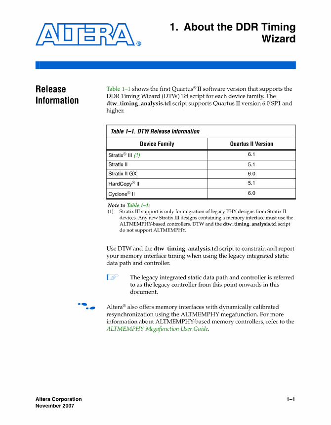
Release Information
Table 1–1 shows the first Quartus® II software version that supports the DDR Timing Wizard (DTW) Tcl script for each device family. The dtw_timing_analysis.tcl script supports Quartus II version 6.0 SP1 and higher.
Use DTW and the dtw_timing_analysis.tcl script to constrain and report your memory interface timing when using the legacy integrated static data path and controller.
1 The legacy integrated static data path and controller is referred to as the legacy controller from this point onwards in this document.
f Altera® also offers memory interfaces with dynamically calibrated resynchronization using the ALTMEMPHY megafunction. For more information about ALTMEMPHY-based memory controllers, refer to the ALTMEMPHY Megafunction User Guide.
Table 1–1. DTW Release Information
Device Family Quartus II Version
Stratix® III (1) 6.1
Stratix II 5.1
Stratix II GX 6.0
HardCopy® II 5.1
Cyclone® II 6.0
Note to Table 1–1:(1) Stratix III support is only for migration of legacy PHY designs from Stratix II
devices. Any new Stratix III designs containing a memory interface must use the ALTMEMPHY-based controllers. DTW and the dtw_timing_analysis.tcl script do not support ALTMEMPHY.
1–1

Device Family Support
Device Family Support
The DTW Tcl script provides full support for the target Altera device families and memory interfaces listed in Table 1–2. In Quartus II software version 6.0 SP1, the dtw_timing_analysis.tcl script was created to supplement DTW. The dtw_timing_analysis.tcl script supports the same device family and external memory interface combinations as the DTW.
Introduction External memory interfaces have timing requirements that must be met for both the FPGA and the memory devices. Some timing requirements, such as controller fMAX, can be analyzed by the Quartus II software and easily met, but some timing requirements need further analysis or manual handling. To meet these timing requirements, you should constrain the placements of the registers or specify timing constraints for the Quartus II software to optimize during compilation.
Background
Previously, the legacy controller MegaWizard generated a script to constrain critical registers for the system called auto_add_ddr_constraints.tcl. This script was used with the verify_timing.tcl script, which was run to verify the system timing based on these constraints. The verify_timing.tcl script, however, made some assumptions that may not have been true for your design. For example, the verify_timing.tcl script assumed that all clocks used for the memory interface were using the global clock networks, so if you used a regional clock network, some of the timing reported by the verify_timing.tcl script may not have been accurate.
Table 1–2. Device Family and External Memory Support for Quartus II version 7.2
Device Family External Memory Supported (2)
Stratix III (1) DDR2/DDR SDRAM, QDRII+/QDRII SRAM, RLDRAM II
Stratix II DDR2/DDR SDRAM, QDRII+/QDRII SRAM, RLDRAM II
Stratix II GX DDR2/DDR SDRAM, QDRII+/QDRII SRAM, RLDRAM II
HardCopy II DDR2/DDR SDRAM, QDRII+/QDRII SRAM, RLDRAM II
Cyclone II DDR2/DDR SDRAM
Notes to Table 1–2:(1) DTW support for Stratix III devices is only for design migration from Stratix II
devices. Any new Stratix III designs containing a memory interface must use the ALTMEMPHY solution. DTW and the dtw_timing_analysis.tcl script do not support ALTMEMPHY.
(2) DTW constrains the data path timing for these memory interfaces. The example driver and the controller are not constrained by the DTW.
1–2 Altera CorporationDDR Timing Wizard User Guide November 2007

About the DDR Timing Wizard
1 The new ALTMEMPHY megafunction, introduced in Quartus II version 6.1 uses timing constraints generated by the ALTMEMPHY MegaWizard, so that you do not need to use DTW to constrain the design. DTW does not support ALTMEMPHY-based memory controllers.
In addition to possible inaccurate assumptions of the design, placement constraints did not work well for designs migrating to HardCopy II or other FPGA devices. When migrating designs, especially to a HardCopy II device, you would need two different sets of placement constraints: one for the FPGA prototype device and one for the HardCopy production device. This also applies when migrating designs to a different FPGA device.
DDR Timing Wizard
The DDR Timing Wizard (DTW) is a Tcl-based GUI that calculates timing constraints based on the FPGA and memory device chosen. It simplifies the process of constraining your design by using timing assignments, which the Quartus II software uses to place and route the design in the target device. These timing constraints are applicable for FPGAs and their HardCopy-equivalent devices, eliminating the need to convert assignments for the different device families (as you would have previously done with the placement constraints from legacy controller MegaWizard). Some critical register placements can be constrained by using LogicLock region assignments, but other than the pin location, output pin load, and I/O standards assignments, you do not need any hard placement constraints. Instead, the timing-driven compilation of the Quartus II software ensures that all DTW timing constraints are met in both FPGA-prototype and HardCopy-production devices.
DTW also gives you the ability to change the pin names of the memory interface to use regional clock networks, and to use TimeQuest Timing Analyzer to analyze the design, which are not supported by the verify_timing.tcl script. DTW constraints also lead to a more accurate timing analysis, as all the information used are based on your particular design, instead of general assumptions made by the MegaWizard. Furthermore, the timing verification script does not report write timing margin. DTW, on the other hand, constrains timing for the write path, allowing Quartus II to analyze the write timing margin. You can then use the dtw_timing_analysis.tcl script to report read, write, address/command, resynchronization, and postamble timing margins that are applicable to your memory interface design. DTW constraints provide more accurate timing results compared to the verify_timing.tcl script.
Altera Corporation 1–3November 2007 DDR Timing Wizard User Guide

Introduction
1 Critical resynchronization register placement constraints provided by the legacy controller MegaWizard can still be used even when DTW is used. You can use LogicLock regions in lieu of hard placement constraints.
1 The results reported by the dtw_timing_analysis.tcl script have no correlation with the verify_timing.tcl script. You should rely on the dtw_timing_analysis.tcl report, as it is more accurate due to the design-specific constraints created by the DTW. The verify_timing.tcl script may have some assumption that does not apply to your particular design.
To use the DTW, you must enter the memory device parameters and your board information correctly in the legacy controller MegaWizard. The Quartus II Fitter uses timing-driven compilation to route the design to meet the timing constraints set by the DTW.
Because the DTW is primarily a constraining tool, the dtw_timing_analysis.tcl script is provided to help you analyze and close timing with a minimum number of compilations. The dtw_timing_analysis.tcl script extracts the system timing margin by re-running timing analysis if needed, adjusting the clock cycles in the DTW (with the -auto_adjust_cycles switch) if required, and suggesting the ideal phase shifts for the system. The dtw_timing_analysis.tcl is backwards-compatible with designs constrained with an older version of DTW. Both DTW and the dtw_timing_analysis.tcl scripts are available in the Quartus II installation directory.
1 If you use the default installation directory, the DTW and dtw_timing_analysis.tcl scripts are available in the c:\altera\<version>\quartus\common\tcl\apps\gui\dtw directory.
1–4 Altera CorporationDDR Timing Wizard User Guide November 2007

About the DDR Timing Wizard
Figure 1–1 shows the typical Quartus II external memory design flow using DTW and the dtw_timing_analysis.tcl script.
Figure 1–1. Quartus II External Memory Design Flow
Note to Figure 1–1:(1) It may be necessary to modify the controller and PHY settings (such as the clock cycles and clock phase shifts) using
the legacy controller or the altpll MegaWizard, based on dtw_timing_analysis.tcl results.
This user guide explains how to constrain designs using DTW, how to analyze the memory interface timing using the dtw_timing_analysis.tcl script, and how to adjust design constraints using the MegaWizard, the Assignment Editor, or DTW to achieve timing closure.
Adjust Constraints Using the MegaWizard, the Assignment Editor,
or the DTW
Instantiate PHYand Controller in a Quartus II Project
Compile Design
Yes Done
Run add_constraints.tcl(Pin Locations,
I/O Standards, and Loading)
Run DTW (Timing Constraints)
Run dtw_timing_analysis.tcl to Get Margin and
Recommended Settings (1)
Add Assignments for Clock, Command, and Address Pin
Locations, and Other Pertinent Assignments for the Interface
No
Is Memory
Interface Timing Met?
Altera Corporation 1–5November 2007 DDR Timing Wizard User Guide
Features
Features The DDR Timing Wizard has the capability to:
■ Constrain a design with one or multiple memory controllers that may reside in subdirectories of the main project.
■ Calculate all of the timing constraints based on your chosen FPGA or HardCopy device, and memory device.
■ Import timing information from the legacy controller MegaWizard.■ Enable timing driven compilation.■ Allow the Quartus II software to analyze and report the
post-compile timing analysis for both fast and slow timing models in one panel.
■ Create both classic timing analyzer and TimeQuest Timing Analyzer assignments for memory interface timing paths.
The dtw_timing_analysis.tcl script complements the DTW with the ability to:
■ Extract and report system timing margin for both fast and slow model timing.
■ Re-run timing analysis using either the Classic Timing Analyzer or TimeQuest Timing Analyzer.
■ Adjust resynchronization and postamble clock cycles in DTW.■ Calculate ideal PLL phase shifts.■ Import legacy controller MegaWizard settings into DTW (with the
option to compile the design after the import).■ Update design tCO information in DTW.
1–6 Altera CorporationDDR Timing Wizard User Guide November 2007
Altera Corporation November 2007
2. Getting Started
System and Software Requirements
The instructions in this section require Quartus II software version 7.2 or higher. DTW and the dtw_timing_analysis.tcl script can be found in the Quartus II installation directory. You can either run the script from that directory or copy the script to your project directory.
1 If you use the default installation directory, the DTW and dtw_timing_analysis.tcl script are available in the c:\altera\<version>\quartus\common\tcl\apps\gui\dtw directory.
Design Flow The design flow when creating a system with external memory interfaces is as follows:
1. Create a memory interface PHY with Altera’s legacy memory controller MegaWizard.
f For more information about how to create a memory controller, refer to the DDR & DDR2 SDRAM Controller Compiler User Guide, QDRII SRAM Controller MegaCore® Function User Guide, and RLDRAM II Controller MegaCore Function User Guide. Follow the instructions up to generating the core, but do not compile the design yet.
f To create an example design, follow the Instantiate PHY and Controller in a Quartus II Project step of the "Example Walkthrough for 267-MHz DDR2 SDRAM Interface using the Legacy PHY" section in AN328: Interfacing DDR2 SDRAM with Stratix II, Stratix II GX, and Arria GX Devices.
If you are not using the Altera memory controller, remove the encrypted controller produced by the legacy controller MegaWizard and connect the Altera-recommended data path from the legacy controller MegaWizard with your memory controller.
2. Run the auto_add_ddr_constraints.tcl script produced by the legacy controller MegaWizard for pin location, I/O standard, output pin load, and register placement assignments for the resynchronization and postamble registers in DDR2/DDR SDRAM interfaces.
2–1
Design Flow
1 You do not need to remove these location assignments when using DTW even though DTW makes the correct timing constraints for the paths to these registers.
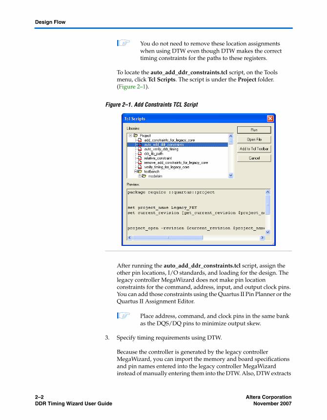
To locate the auto_add_ddr_constraints.tcl script, on the Tools menu, click Tcl Scripts. The script is under the Project folder. (Figure 2–1).
Figure 2–1. Add Constraints TCL Script
After running the auto_add_ddr_constraints.tcl script, assign the other pin locations, I/O standards, and loading for the design. The legacy controller MegaWizard does not make pin location constraints for the command, address, input, and output clock pins. You can add those constraints using the Quartus II Pin Planner or the Quartus II Assignment Editor.
1 Place address, command, and clock pins in the same bank as the DQS/DQ pins to minimize output skew.
3. Specify timing requirements using DTW.
Because the controller is generated by the legacy controller MegaWizard, you can import the memory and board specifications and pin names entered into the legacy controller MegaWizard instead of manually entering them into the DTW. Also, DTW extracts
2–2 Altera CorporationDDR Timing Wizard User Guide November 2007
Getting Started
the names of the PLL clocks and registers (as needed) for the timing requirements. It also extracts the phase shifts of synthesized PLLs. The step-by-step instructions are listed in “Import Flow for the Altera Legacy Memory Controller IP Core or Recommended Data Path” on page 2–7.
1 You may need to re-run DTW and compile the design multiple times before achieving timing closure. You can close timing within two compiles if you do not need to change the intermediate registers option in the legacy controller MegaWizard.
4. Add other assignments for the design.
Add the following assignments in the Assignment Editor (unless indicated otherwise) to the project before you compile the design:
● If you are using classic Timing Analyzer:
• In the Settings tab of the Assignment menu, uncheck the Optimize hold timing option.
• In the Settings tab of the Assignment menu, uncheck the Optimize fast corner timing option.
This disallows the Quartus II Fitter from optimize placement each time the project is recompiled. Having these options enabled may render your phase shift changes invalid because the Quartus II Fitter has the priority to optimize for hold timing and fast cornering.
You can re-enable the Optimize hold timing and Optimize fast corner timing options for the remainder of the design after you close timing on your memory interface. To ensure the memory interface part of the design has similar timing, back-annotate placements and routing for that portion of the design before re-enabling the options.
● If you are using TimeQuest Timing Analyzer, add the DTW-generated .sdc file to the project.
● Set the delay from Output Register to Output Pin to 0 for the CK/CK# (clk_to_sdram*) clock outputs and fedback clock output.
● Assign pin constraints for all the CK/CK# and feedback output pins and ensure that the feedback output pins use the same I/O
Altera Corporation 2–3November 2007 DDR Timing Wizard User Guide

Design Flow
standard as the CK/CK# pins, and are placed on the same side as the DQS/DQ pins.
● Assign pin location, I/O standard, and output pin load constraints for clock_source, feedback input pins, and address and command pins.
● For RLDRAM II memory interfaces created in Quartus II version 7.2 and higher, add the <variation_name>_controller.sdc file to the project
● For QDRII+/QDRII SRAM memory interfaces using TimeQuest Timing Analyzer, convert the setup_relationship and hold_relationship MegaWizard-generated constraints to SDC constraints. The setup_relationship and hold_relationship assignment can be directly converted to set_max_delay and set_min_delay assignments, as shown in the below example:
set_max_delay -0.2 -from * -to <resync_registers*>set_min_delay -1.6 -from * -to <resync_registers*>
5. Compile the design.
6. Check the timing analysis results.
After completing a DTW design compilation, refer to Chapter 3, Using the dtw_timing_analysis.tcl Script for information about analyzing the memory interfaces.
If problem paths are reported, locate and fix them to maximize setup and hold slack. For example, you can:
● Adjust PLL clock phases with the legacy controller or the altpll MegaWizard.
1 Note that some clock phases can only be changed in the legacy controller MegaWizard, especially for shared PLL outputs. For example, if your postamble clock was set to 90° initially, but you want to change it to use either a dedicated clock or a 180° phase shift.
● Insert or remove intermediate resynchronization and/or postamble registers in the legacy controller MegaWizard.
2–4 Altera CorporationDDR Timing Wizard User Guide November 2007

Getting Started
1 You need to insert intermediate resynchronization registers when you have negative margin in the transfer between resynchronization registers and the registers clocked by the system clock. The dtw_timing_analysis.tcl script will tell you when to add or remove the intermediate postamble registers.
● Change the data path resynchronization and/or postamble clock cycles in the legacy controller MegaWizard.
● Change location assignments to the problem PLL clocks, I/O pins, or registers.
f Refer to Chapter 3, Using the dtw_timing_analysis.tcl Script for information on how to fix your timing violations using the dtw_timing_analysis.tcl script.
1 If you need to change any PLL phase shifts, re-run the Quartus II Analysis and Synthesis to refresh the PLL settings before importing the new phase shift in the DTW. You can click on the Start Analyze & Synthesis button manually or use the –after_iptb import option in the dtw_timing_analysis.tcl script. You can also enter the PLL phase shifts manually in the DTW to bypass Quartus II Analysis and Synthesis. However, DTW will not be able to confirm if the phase shift entered is the correct phase shift that is implemented in the design.
If there are no failing paths, your design is complete. Otherwise, go back to step 5 after making the necessary timing requirements changes until the design achieves timing closure.
Launching the DDR Timing Wizard
To launch the DDR Timing Wizard from the Quartus II software, follow these steps:
1. On the Tools menu, click Tcl Scripts.
2. In the Tcl Scripts dialog box, under Libraries, expand the <installation_directory>/quartus/common/tcl/apps/gui/dtw folder, select dtw (Figure 2–2).
Altera Corporation 2–5November 2007 DDR Timing Wizard User Guide
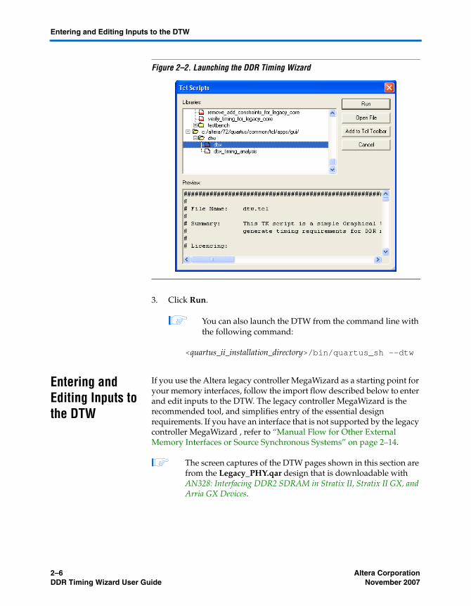
Entering and Editing Inputs to the DTW
Figure 2–2. Launching the DDR Timing Wizard
3. Click Run.
1 You can also launch the DTW from the command line with the following command:
<quartus_ii_installation_directory>/bin/quartus_sh --dtw
Entering and Editing Inputs to the DTW
If you use the Altera legacy controller MegaWizard as a starting point for your memory interfaces, follow the import flow described below to enter and edit inputs to the DTW. The legacy controller MegaWizard is the recommended tool, and simplifies entry of the essential design requirements. If you have an interface that is not supported by the legacy controller MegaWizard , refer to “Manual Flow for Other External Memory Interfaces or Source Synchronous Systems” on page 2–14.
1 The screen captures of the DTW pages shown in this section are from the Legacy_PHY.qar design that is downloadable with AN328: Interfacing DDR2 SDRAM in Stratix II, Stratix II GX, and Arria GX Devices.
2–6 Altera CorporationDDR Timing Wizard User Guide November 2007

Getting Started
1 You do not need to perform Quartus II Analysis and Synthesis the first time you run DTW as this has been done when running the auto_add_ddr_constraints.tcl script. However, any subsequent calls to the DTW must be preceded with a Quartus II Analysis and Synthesis process, otherwise DTW will not be able to read any changes to the design.
Import Flow for the Altera Legacy Memory Controller IP Core or Recommended Data Path
When you use the Altera-provided data path, you can benefit by importing the memory data path settings, which saves time because parameters required by the DTW do not need to be filled in manually. If you choose to create your own data path, you can find more information about the DTW pages in “Manual Flow for Other External Memory Interfaces or Source Synchronous Systems” on page 2–14.
The following procedure illustrates a DDR/DDR2 SDRAM interface example, but the steps are identical for the QDRII+/QDRII SRAM or the RLDRAM II interface. Before performing the following steps, be sure to run the legacy controller MegaWizard auto_add_ddr_constraints.tcl script and run Quartus II Analysis and Synthesis.
After launching the DTW, follow these steps to import the timing parameters and pin names from the legacy controller MegaWizard:
1. On the first page of the DTW, you are prompted to create or edit a .dwz file. Opening the DTW allows you to make changes to the saved .dwz file or to create a new .dwz file. This file contains all of the parameters you enter in the DTW script.
Figure 2–3 shows the first page of the DTW software in which you can specify the location for the .dwz file. The default name and location for the file is:
<quartus_ii_project_directory>/ddr_settings.dwz
Ensure that the .dwz file points to the project directory that you are working on. If you have un-archived the project, the .dwz file may still be pointing to the old project directory. You can change the file name and click Next.
1 The saved file name always defaults to ddr_setting.dwz. Ensure that it is the file name you want to use. If you have multiple memory controllers in a design, you must have a unique .dwz file name for each controller.
Altera Corporation 2–7November 2007 DDR Timing Wizard User Guide

Entering and Editing Inputs to the DTW
Figure 2–3. First Page of the DDR Timing Wizard—Create or Edit File
2. Page 2 of the DTW (Figure 2–4) asks you to confirm the project directory and the revision you want to use. (Note that the project name is case-sensitive.) The DTW automatically fills in the fields, but you can change those fields if the project has been moved or if you have a newer revision. Click Next.
2–8 Altera CorporationDDR Timing Wizard User Guide November 2007

Getting Started
Figure 2–4. Page 2 of the DTW—Confirm the Project Directory and Revision Name
3. Figure 2–5 shows page 3 of the DTW. This page asks whether you would like to import data from the legacy controller MegaWizard instance using Classic Timing Analyzer or TimeQuest Timing Analyzer names.
If you choose TimeQuest Timing Analyzer names, DTW creates assignments that are stored in an .sdc file. Choosing Classic Timing Analyzer names generates both .qsf assignments and an .sdc file. This means that you can still use TimeQuest Timing Analyzer for compilation and timing analysis even when you choose Classic Timing Analyzer names.
You need to add the .sdc file to the project when using TimeQuest Timing Analyzer for compilation and timing analysis.
1 The difference between the .sdc file created using Classic Timing Analyzer and TimeQuest Timing Analyzer names is the clock name convention. There should not be any difference in timing analysis results between these two .sdc files.
1 You should use TimeQuest Timing Analyzer for a more accurate timing analysis as the constraints of the .sdc file apply to both fast and slow timing models.
Click Import.
Altera Corporation 2–9November 2007 DDR Timing Wizard User Guide
Entering and Editing Inputs to the DTW
Figure 2–5. Page 3 of the DTW—Importing Data from the Legacy Controller MegaWizard
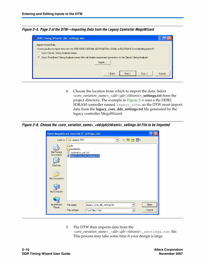
4. Choose the location from which to import the data. Select <core_variation_name>_<ddr|qdr|rldramii>_settings.txt from the project directory. The example in Figure 2–6 uses a the DDR2 SDRAM controller named legacy_core, so the DTW must import data from the legacy_core_ddr_settings.txt file generated by the legacy controller MegaWizard.
Figure 2–6. Choose the <core_variation_name>_<ddr|qdr|rldramii>_settings.txt File to be Imported
5. The DTW then imports data from the <core_variation_name>_<ddr|qdr|rldramii>_settings.txt file. This process may take some time if your design is large.
2–10 Altera CorporationDDR Timing Wizard User Guide November 2007

Getting Started
1 The DTW can extract the names of PLL clocks, PLL phase shifts, and names of registers, if you have already run the Quartus II Analysis and Synthesis. The auto_add_ddr_constraints.tcl script automatically analyzes and synthesizes the design, so you do not have to perform Quartus II Analysis and Synthesis the first time you invoke DTW after running the auto_add_ddr_constraints.tcl script. However, any time you make a change in the PLL or the legacy controller MegaWizard, you need to analyze and synthesize the design before invoking DTW, so that DTW can extract the correct clock names and phase shifts when performing an Import function.
When the import is complete, click Skip to get to the last page of DTW.
1 Instead of skipping to the end, you can verify the values in the DTW by clicking Next and checking each page of the DTW to ensure that everything is imported correctly. These pages are described in detail in “Manual Flow for Other External Memory Interfaces or Source Synchronous Systems” on page 2–14.
At this point, if the DTW has all of the needed information, a page similar to the one shown in Figure 2–7 appears. Click Finish.
Altera Corporation 2–11November 2007 DDR Timing Wizard User Guide

Entering and Editing Inputs to the DTW
Figure 2–7. Timing Assignments to be Added to the Project
When using Classic Timing Analyzer, the last page of the DTW names looks a little different than Figure 2–7. This is described in more detail in “Manual Flow for Other External Memory Interfaces or Source Synchronous Systems” on page 2–14.
2–12 Altera CorporationDDR Timing Wizard User Guide November 2007
Getting Started
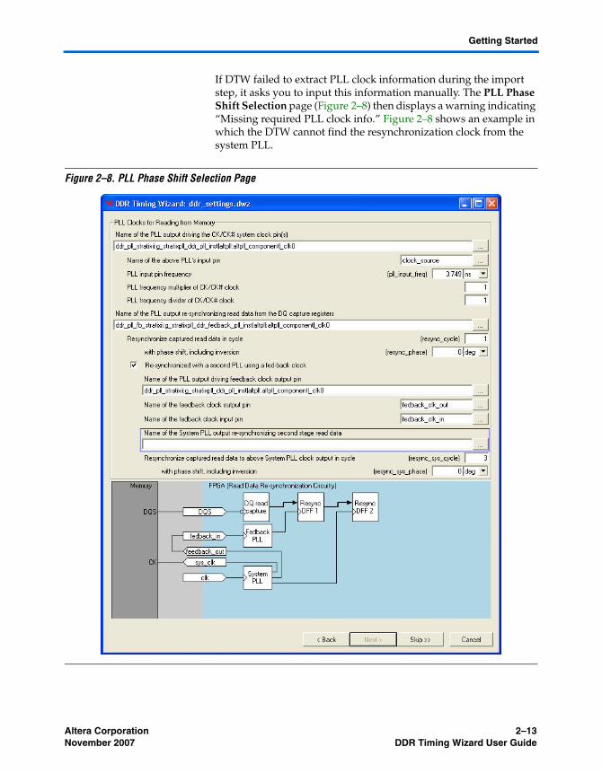
If DTW failed to extract PLL clock information during the import step, it asks you to input this information manually. The PLL Phase Shift Selection page (Figure 2–8) then displays a warning indicating “Missing required PLL clock info.” Figure 2–8 shows an example in which the DTW cannot find the resynchronization clock from the system PLL.
Figure 2–8. PLL Phase Shift Selection Page
Altera Corporation 2–13November 2007 DDR Timing Wizard User Guide

Entering and Editing Inputs to the DTW
After entering the resynchronization clock name (omitted in Figure 2–8) click Skip to get to the last page of DTW.
Click Finish.
6. Add the additional assignments as listed on Step 4 of the “Design Flow” section.
7. Compile the design and perform timing analysis.
f For more details, refer to Chapter 3, Using the dtw_timing_analysis.tcl Script.
Manual Flow for Other External Memory Interfaces or Source Synchronous Systems
Use this flow when you have a custom implementation for an Altera-supported memory interface, including the following:
■ DDR/DDR2 SDRAM■ QDRII+/QDRII SRAM■ RLDRAM II
1 Always implement the Altera data path and use the legacy controller MegaWizard flow unless the feature set of the Altera memory controller makes it impossible to do so.
The DTW Pages for DDR/DDR2 SDRAM
This section details each page in the DDR/DDR2 SDRAM interface. The pages for QDRII+/QDRII SRAM and RLDRAM II interfaces are slightly different than the pages for DDR/DDR2 SDRAM interfaces. The DTW pages for QDRII+/QDRII SRAM and RLDRAM II are listed in “The DTW Pages for QDRII+/QDRII SRAM & RLDRAM II” on page 2–45.
1 The following page-by-page information is based from a controller created by the legacy controller MegaWizard but the DTW import option is not used.
1. On the Tools menu, select Tcl Scripts. Select dtw and click Run.
2. Specify a .dwz file name to save the timing constraints for the design and click Next.
3. Confirm the project directory and revision you want to use.
Click Next.
2–14 Altera CorporationDDR Timing Wizard User Guide November 2007

Getting Started
4. Page 3 asks if you want to import data from the legacy controller MegaWizard, and whether you want to use TimeQuest or Classic Timing Analyzer names. Click on one of the radio buttons (even if you are not using the Import function) and click Next.
5. Select your memory type: DDR/DDR2 SDRAM, QDRII+/QDRII SRAM or RLDRAM II. For this example, choose DDR/DDR2 SDRAM. Refer to Figure 2–9.
Altera Corporation 2–15November 2007 DDR Timing Wizard User Guide

Entering and Editing Inputs to the DTW
Figure 2–9. Select Memory Type
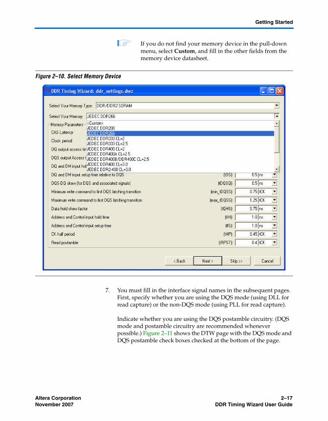
6. Select the appropriate memory device from the drop-down menu (Figure 2–10).
The rest of the fields are filled in automatically when you pick a device. Click Next.
2–16 Altera CorporationDDR Timing Wizard User Guide November 2007
Getting Started
1 If you do not find your memory device in the pull-down menu, select Custom, and fill in the other fields from the memory device datasheet.
Figure 2–10. Select Memory Device
7. You must fill in the interface signal names in the subsequent pages. First, specify whether you are using the DQS mode (using DLL for read capture) or the non-DQS mode (using PLL for read capture).
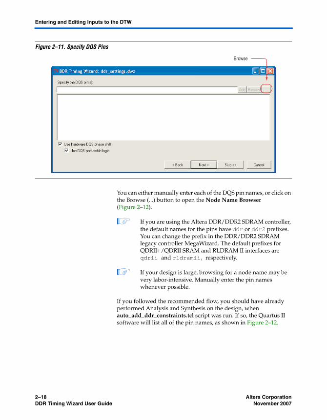
Indicate whether you are using the DQS postamble circuitry. (DQS mode and postamble circuitry are recommended whenever possible.) Figure 2–11 shows the DTW page with the DQS mode and DQS postamble check boxes checked at the bottom of the page.
Altera Corporation 2–17November 2007 DDR Timing Wizard User Guide
Entering and Editing Inputs to the DTW
Figure 2–11. Specify DQS Pins
You can either manually enter each of the DQS pin names, or click on the Browse (...) button to open the Node Name Browser (Figure 2–12).
1 If you are using the Altera DDR/DDR2 SDRAM controller, the default names for the pins have ddr or ddr2 prefixes. You can change the prefix in the DDR/DDR2 SDRAM legacy controller MegaWizard. The default prefixes for QDRII+/QDRII SRAM and RLDRAM II interfaces are qdrii and rldramii, respectively.
1 If your design is large, browsing for a node name may be very labor-intensive. Manually enter the pin names whenever possible.
If you followed the recommended flow, you should have already performed Analysis and Synthesis on the design, when auto_add_ddr_constraints.tcl script was run. If so, the Quartus II software will list all of the pin names, as shown in Figure 2–12.
Browse
2–18 Altera CorporationDDR Timing Wizard User Guide November 2007

Getting Started
If you have not performed Analysis and Synthesis on the design, the Node Name Browser page will not have any nodes listed under Nodes Found. If this is the case, click on the Analysis and Synthesis button (Figure 2–12).
Figure 2–12. Node Name Browser of a Sample DDR2 SDRAM Interface
To use the node name browser to add the DQS pin names, perform the following steps:
a. Highlight the DQS pin names under Nodes Found and click the arrow button to move the pins to the Selected Nodes field (Figure 2–13 and Figure 2–14).
Analysis & Synthesis
Altera Corporation 2–19November 2007 DDR Timing Wizard User Guide

Entering and Editing Inputs to the DTW
Figure 2–13. Selecting the DQS Pins
Figure 2–14. DQS Pins Selected
2–20 Altera CorporationDDR Timing Wizard User Guide November 2007
Getting Started
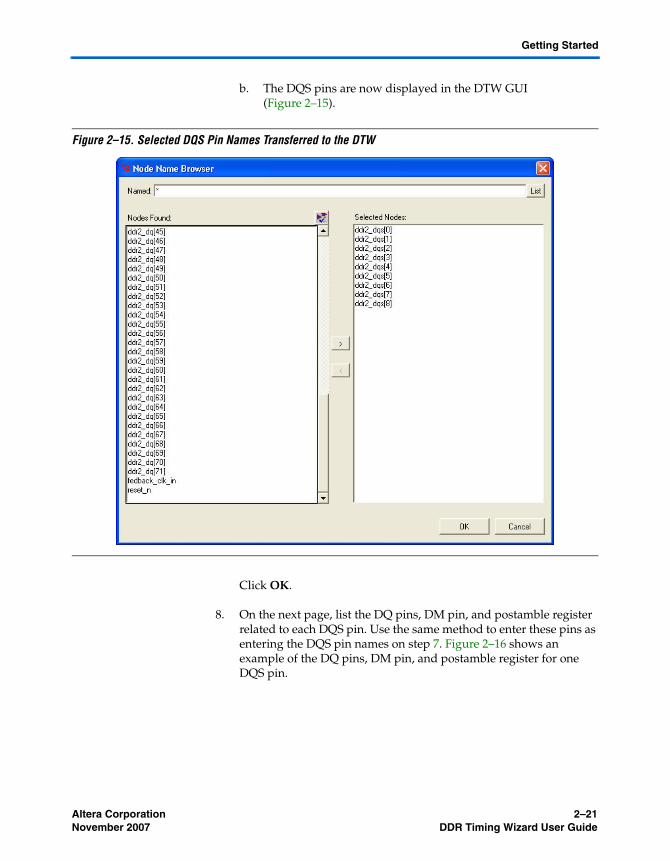
b. The DQS pins are now displayed in the DTW GUI (Figure 2–15).
Figure 2–15. Selected DQS Pin Names Transferred to the DTW
Click OK.
8. On the next page, list the DQ pins, DM pin, and postamble register related to each DQS pin. Use the same method to enter these pins as entering the DQS pin names on step 7. Figure 2–16 shows an example of the DQ pins, DM pin, and postamble register for one DQS pin.
Altera Corporation 2–21November 2007 DDR Timing Wizard User Guide

Entering and Editing Inputs to the DTW
1 The postamble register name from the Altera DDR2/DDR SDRAM controller is listed in Figure 2–16. You can find this register using the Node Finder in the Assignment Editor. You can then copy the register name and add it into the postamble register field. In designs targeting Stratix II, Stratix II GX, Arria GX, or Hardcopy II devices, search for these text in the Node Finder to find the postamble registers: *dqs_io~regout*
After you enter the pins’ and registers’ names for each DQS pin, click Next.
Figure 2–16. Sample Page of DQ Pins, DM Pin and Postamble Register for One DQS Pin
2–22 Altera CorporationDDR Timing Wizard User Guide November 2007
Getting Started
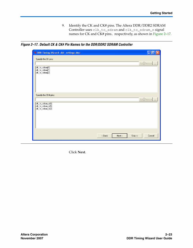
9. Identify the CK and CK# pins. The Altera DDR/DDR2 SDRAM Controller uses clk_to_sdram and clk_to_sdram_n signal names for CK and CK# pins, respectively, as shown in Figure 2–17.
Figure 2–17. Default CK & CK# Pin Names for the DDR/DDR2 SDRAM Controller
Click Next.
Altera Corporation 2–23November 2007 DDR Timing Wizard User Guide
Entering and Editing Inputs to the DTW
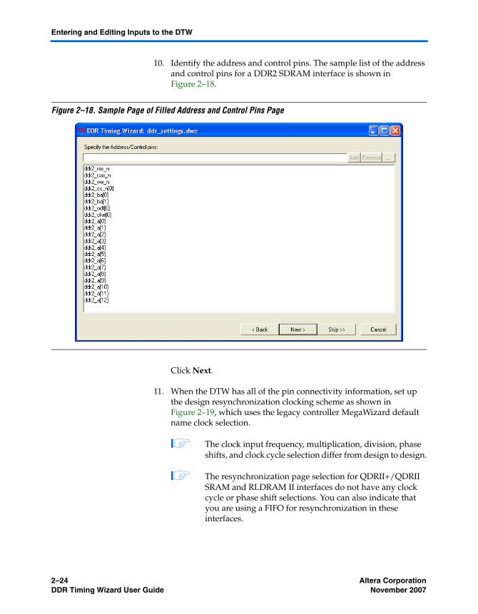
10. Identify the address and control pins. The sample list of the address and control pins for a DDR2 SDRAM interface is shown in Figure 2–18.
Figure 2–18. Sample Page of Filled Address and Control Pins Page
Click Next.
11. When the DTW has all of the pin connectivity information, set up the design resynchronization clocking scheme as shown in Figure 2–19, which uses the legacy controller MegaWizard default name clock selection.
1 The clock input frequency, multiplication, division, phase shifts, and clock cycle selection differ from design to design.
1 The resynchronization page selection for QDRII+/QDRII SRAM and RLDRAM II interfaces do not have any clock cycle or phase shift selections. You can also indicate that you are using a FIFO for resynchronization in these interfaces.
2–24 Altera CorporationDDR Timing Wizard User Guide November 2007

Getting Started
f Refer to Appendix A of the DDR and DDR2 SDRAM Controller Compiler User Guide for more information on the resynchronization and postamble clock cycles and phase shifts.
Figure 2–19. Resynchronization Clock Connectivity
Altera Corporation 2–25November 2007 DDR Timing Wizard User Guide

Entering and Editing Inputs to the DTW
1 The default TimeQuest Timing Analyzer clocking names are shown in Figure 2–19. If you are using Classic Timing Analyzer, the default clocking names for the system PLL are:
ddr_pll_stratixii:g_stratixpll_ddr_pll_inst|altpll:altpll_component|_clkn
where n denotes the PLL output counter number.
Clicking on a field in this page highlights the location of that field in the design schematic in the bottom of the page. For example, if you click on the resync_cycle field as shown in Figure 2–20, the path from the system PLL to the Resync DFF1 is highlighted to show where the resync_cycle information is used. The DTW shows a different schematic if the interface is using 1-PLL mode.
1 You can use the highlights as a guide when you must enter each field manually. The design schematic varies depending on the interface mode, whether you are using DQS, or whether you are using 2-PLL (with the fedback PLL) or 1-PLL mode. This example design uses DQS with 2-PLL implementation.
2–26 Altera CorporationDDR Timing Wizard User Guide November 2007

Getting Started
Figure 2–20. Fedback Resynchronization Path (Highlighted)
The first field of this page asks for the name of the PLL output generating the CK/CK# system clock pins. Typically, this clock is the system clock, which also drives the controller. However, if you are using the dedicated clock output pins without the DDIO circuitry as required in HardCopy II devices, you may need a separate PLL output to ensure that tDQSS is met at both fast and slow timing models.
Altera Corporation 2–27November 2007 DDR Timing Wizard User Guide
Entering and Editing Inputs to the DTW
f Refer to AN 413: Using Legacy Integrated Static Data Path and Controller Megafunction with HardCopy Structured ASICs on how to generate CK/CK# signals using dedicated clock outputs.
You then must enter the PLL input clock name and the multiplication and division factors to achieve the memory interface frequency of operation. In Figure 2–19, the design uses a 100-MHz input clock, so the multiplication and division factors are set to 8 and 3, respectively, to interface with a 267-MHz DDR2 SDRAM DIMM.
The name of the PLL output resynchronizing read data from the read capture registers depends on whether you are using the 2-PLL mode or the 1-PLL mode. The example design uses the 2-PLL mode, so the PLL output resynchronizing read data from the read capture registers that comes from the fedback PLL.
In 2-PLL mode, the DTW must know the clock cycle of the fedback resynchronization clock and the system (second) resynchronization clock. The legacy controller MegaWizard only provides the clock cycle for the system resynchronization clock, so the DTW has to calculate the fedback resynchronization clock cycle (resync_cycle) in 2-PLL mode.
1 In 1-PLL mode, there is only one clock cycle information required since there is only one resynchronization clock. This clock cycle is also called resync_cycle and is provided by the legacy controller MegaWizard.
Because the DTW must know the clock cycle and the clock phase shift for each data transfer, there is a register transfer between the fedback PLL resynchronization clock and the system PLL resynchronization clock in 2-PLL mode interfaces. The legacy controller MegaWizard only needs to know the clock cycle on the system PLL side, so the DTW manually calculates this in 2-PLL mode. The legacy controller MegaWizard provides this number in 1-PLL mode since there is only one resynchronization clock from the system PLL in this implementation.
The resync_phase field should match the phase shift entered in the legacy controller MegaWizard in the Fed-back clock phase field. An example of the proper name for a PLL clock output for resynchronization clock is shown in Figure 2–20. See Figure 2–21 for matching each resynchronization field in the legacy controller MegaWizard in the DTW.
2–28 Altera CorporationDDR Timing Wizard User Guide November 2007

Getting Started
Figure 2–21. Resynchronization Clock and Phase Shift Relationship in DTW and the DDR2/DDR SDRAM Controller MegaWizard
The Resynchronized with a second PLL using a fed-back clock field must be checked when using the fedback-clock mode, as the controlller uses this clock before resynchronizing data back to the system clock domain. You then must specify the fedback clock input and output pins, as well as the name of the system PLL output clock to resynchronize the data from the fedback PLL to the system PLL. The clock cycle (resync_sys_cycle) and clock phase shift (resync_sys_phase) in this section should match with the legacy controller MegaWizard information. If not, you need to fix this information in DTW. After running the dtw_timing_analysis.tcl
Altera Corporation 2–29November 2007 DDR Timing Wizard User Guide

Entering and Editing Inputs to the DTW
with the –auto_adjust_cycles option, the DTW will have the best clock cycle settings, so you need to update the legacy controller MegaWizard at that point if the numbers do not match.
Table 2–1 shows the relationship between the legacy controller MegaWizard and the DTW, in terms of resynchronization clock cycles and phase shifts.
Click Next.
12. Figure 2–22 shows the DTW page for postamble clock connectivity. The name of the PLL output driving the read postamble reset control clock can come from the system PLL (when using 1-PLL mode) or the fedback PLL (when using the fedback-clock mode). Similar to the the resync_cycle field, the postamble_cycle field is calculated by DTW when using the fedback-clock mode, but is from the legacy controller MegaWizard when using one PLL only. The postamble_phase is the postamble phase shift you entered in legacy controller MegaWizard when you created the data path or controller.
Table 2–1. Legacy Controller MegaWizard and DTW Resynchronization Clock Cycles
DTW Resynchronization Fields
Interfaces with One PLL (≤ 200 MHz)
Interfaces with Fedback-Clock Mode (> 200 MHz) (1)
resync_cycle From the Resynchronize captured read data in cycle field in the legacy controller MegaWizard Manual Timings tab
Calculated by DTW
resync_phase From the Dedicated clock phase field in the legacy controller MegaWizard Manual Timings tab
From the Fed-back clock phase field in the legacy controller MegaWizard Manual Timings tab
resync_sys_cycle Not used From the Resynchronize captured read data in cycle field in the legacy controller MegaWizard Manual Timings tab
resync_sys_phase Not used From the Dedicated clock phase field in the legacy controller MegaWizard Manual Timings tab
Note to Table 2–1:(1) For new designs targeting memory interfaces higher than 200 MHz, Altera recommends using the
high-performance controller featuring the ALTMEMPHY megafunction in the Quartus II software.
2–30 Altera CorporationDDR Timing Wizard User Guide November 2007

Getting Started
Figure 2–22. Postamble Clock Connectivity
The postamble_sys_cycle and postamble_sys_phase are specific to the fedback-clock mode implementation. The postamble_sys_cycle information should match with the number in the legacy controller MegaWizard. The postamble_sys_phase, however, depends on whether the option to use intermediate postamble registers is checked in the legacy controller MegaWizard or not. When the option is checked, postamble_sys_phase is set to 0°. When the option is not checked in the design, postamble_sys_phase is set to –180°.
Altera Corporation 2–31November 2007 DDR Timing Wizard User Guide

Entering and Editing Inputs to the DTW
Table 2–2 shows the relationship between the legacy controller MegaWizard and the DTW in terms of postamble clock cycles and phase shifts. This relationship for a 2-PLL mode example is also shown in Figure 2–23.
Table 2–2. Relationship Between the Legacy Controller MegaWizard and the DTW
DTW Postamble Fields Interfaces with One PLL (≤ 200 MHz)
Interfaces with Fedback-Clock Mode (> 200 MHz) (1)
postamble_cycle From the Postamble cycle field in the legacy controller MegaWizard Manual Timings tab
Calculated by DTW
postamble_phase From the Dedicated clock phase field in the legacy controller MegaWizard Manual Timings tab
From the Dedicated clock phase field in the legacy controller MegaWizard Manual Timings tab
postamble_sys_cycle Not used From the “Postamble cycle” field in the legacy controller MegaWizard Manual Timings tab
postamble_sys_phase Not used 0° or -180° whether intermediate postamble registers are used or not.
Note to Table 2–2:(1) For new designs targeting memory interfaces higher than 200 MHz, Altera recommends using the
high-performance controller featuring the ALTMEMPHY megafunction in the Quartus II software.
2–32 Altera CorporationDDR Timing Wizard User Guide November 2007
Getting Started
Figure 2–23. Postamble Clock and Phase Shift Relationship in DTW and the DDR2/DDR SDRAM Controller MegaWizard
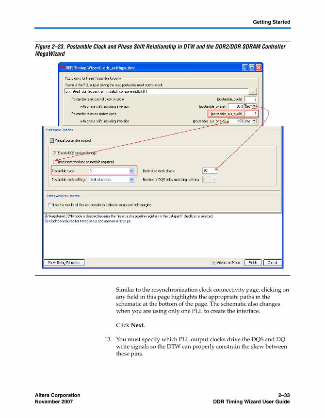
Similar to the resynchronization clock connectivity page, clicking on any field in this page highlights the appropriate paths in the schematic at the bottom of the page. The schematic also changes when you are using only one PLL to create the interface.
Click Next.
13. You must specify which PLL output clocks drive the DQS and DQ write signals so the DTW can properly constrain the skew between these pins.
Altera Corporation 2–33November 2007 DDR Timing Wizard User Guide

Entering and Editing Inputs to the DTW
You also must specify which PLL output clock drives the address and control signals so the DTW can constrain the skew between those pins and the CK/CK# pins properly. The Altera DDR/DDR2 SDRAM controller uses clk0 and clk1 of the system PLL to generate DQS and DQ signals, respectively, as shown in Figure 2–25.
Figure 2–24. Default Clock Selection for the Altera DDR/DDR2 SDRAM Controller
Click Next.
14. Figure 2–25 shows the DTW page in which you specify board trace lengths. This information is required to calculate the resynchronization and postamble clock phase shifts. The DDR/DDR2 SDRAM legacy controller MegaWizard has some default values (as shown in Figure 2–25); however, you should enter the accurate trace lengths, skew, and board tolerance so that the DTW can calculate the correct timing constraints for your data resynchronization and postamble clocks.
1 It is preferred that the trace delay information is extracted from the board design with a signal integrity tool. If you can only provide trace lengths and a constant scaling factor (for example, 166 ps/in), the timing margin analysis will not be as accurate. The flight time information should be the nominal delay for each signal, but you also need to determine a global tolerance for these numbers as well. If an accurate number cannot be provided for that tolerance, the DTW defaults to ±5%. Note that if you use a signal integrity tool to generate the signal delays, you should set the Output Pin Load setting to 0 pF since that load capacitance is factored into the signal delay.
2–34 Altera CorporationDDR Timing Wizard User Guide November 2007

Getting Started
DTW requires the following numbers to be entered:
● Nominal memory to FPGA trace (DQ and DQS traces)
The midpoint between the maximum DQ/DQS trace delay and the minimum DQ/DQS trace delay, using typical delays. For example:
nominal_tpd (memory_to_FPGA) = (max(DQ, DQS) + min (DQ, DQS)) / 2.
● Nominal FPGA output to memory trace
The midpoint between the maximum CK/CK# trace delay and the minimum CK/CK# trace delay, using typical delays. For example:
nominal_tpd (FPGA_to_memory) = (max(CK, CK#) + min (CK, CK#)) / 2.
● Nominal feedback clock trace
The average delay of the two differential feedback clock traces. For example:
nominal_tpd (feedback_trace) = (feedback_clock_p + feedback_clock_n) / 2
For a single-ended feedback clock, just use the delay of that clock trace.
● Board tolerance (measurement error in the above delays)
Maximum ± percent variation of the trace delays due to board manufacturing tolerances and environmental conditions. Note the other board delays specified use typical delays that do not include these variations.
● Skew between wires in a data group (maximum delay difference between DQS and DQ/DM board traces)
Maximum difference of DQ and DM board traces relative to DQS/DQS# board traces.
Altera Corporation 2–35November 2007 DDR Timing Wizard User Guide

Entering and Editing Inputs to the DTW
● Skew between wires in an address/control group (maximum delay difference between CK/CK# and address/control wires)
Maximum difference of BA, A, RAS#, CAS#, WE#, CS#, CKE, and ODT board traces relative to CK/CK# board trace.
● Skew between CK/CK# and DQS outputs
Maximum difference of CK/CK# board traces relative to DQS/DQS# board traces.
Figure 2–25. Board Information Page with Default Legacy Controller MegaWizard Values
Click Next.
15. The next two pages, which are also the last two pages of the DTW, are dependent on whether you are using TimeQuest or Classic Timing Analyzer names. The second-to-last page shows the FPGA parameters used for the interface, while the last page shows a summary of the assignment as well as the location of the files that contain the assignment.
Figure 2–26 and Figure 2–27 show the FPGA parameter page of the DTW when you are using TimeQuest or Classic Timing Analyzer names, respectively. Both figures show a clock uncertainty section with an option to use explicit clock uncertainties for HardCopy II devices.
2–36 Altera CorporationDDR Timing Wizard User Guide November 2007

Getting Started
Figure 2–26. FPGA Timing Parameters When Using TimeQuest Timing Analyzer Names
Altera Corporation 2–37November 2007 DDR Timing Wizard User Guide
Entering and Editing Inputs to the DTW
Figure 2–27. FPGA Timing Parameters Page When Using Classic Timing Analyzer Names
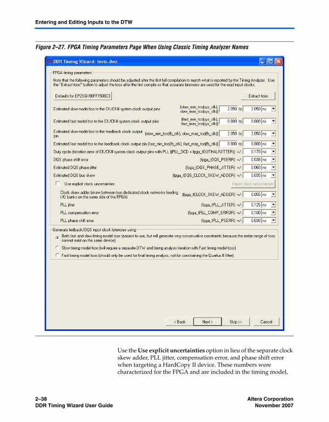
Use the Use explicit uncertainties option in lieu of the separate clock skew adder, PLL jitter, compensation error, and phase shift error when targeting a HardCopy II device. These numbers were characterized for the FPGA and are included in the timing model,
2–38 Altera CorporationDDR Timing Wizard User Guide November 2007

Getting Started
while in HardCopy II, these numbers need to be calculated separately based on the design. HardCopy II designs must use this explicit clock uncertainties option. When the option is not checked, as in Figure 2–26 and Figure 2–27, you specify the clock skew adder, PLL jitter, compensation error, and phase shift error individually. DTW automatically populates these fields based on the synthesized design. When the option is checked, the individual numbers are added up to create clock uncertainty requirements for data capture, fedback-clock resynchronization, write data, address, and tDQSS specifications.
When the Use explicit clock uncertainties option is checked, you must import clock uncertainties from the HardCopy II Clock Uncertainty Calculator. The calculator is available by request when you have a design with memory interfaces targeting HardCopy II devices. You should have used this calculator before the design review process. Contact your Field Applications Engineers (FAEs) for access to the calculator.
f The duty cycle distortion, PLL uncertainties, DQS uncertainties, and skew parameters are specified in the Stratix II Device Handbook.
Figure 2–27 also display estimated tCO numbers for the clocks. These are only used when using Classic Timing Analyzer as DTW uses tCO skew to determine the write timing constraints. The numbers shown in Figure 2–27 are pre-compiled tCO estimates that the DTW uses to generate the timing constraints before the design in compiled. After you compile the design, rerun the DTW and click the Extract tcos button to use actual timing data for more accurate timing constraints. (Note that this process may take some time if your design is large.) You can also use the -extract_tcos yes option when running dtw_timing_analysis.tcl. Click on the Defaults for <device> button to reset any of the numbers with the pre-compiled numbers.
1 Extract tcos assumes that you are using DDIOs for your memory clocks. If you are targeting HardCopy II, you need to use dedicated PLL clock outputs for your memory clocks. In this case, you have to manually enter the CK/CK# tCOs for both timing models.
The bottom of Figure 2–27 shows the option to either use Both fast and slow timing model tcos or to use Slow timing model tcos and Fast timing model tcos separately. You can use either mode, but Altera recommends using the separate timing model for memory interface designs running at or above 200 MHz.
Altera Corporation 2–39November 2007 DDR Timing Wizard User Guide

Entering and Editing Inputs to the DTW
When you check the option to use Both fast and slow timing model tcos, DTW uses the fastest tCO from the fast model and slowest tCO from the slow model to generate constraints for resynchronization and postamble paths. This means that you may be over-constraining your design since both the fastest and slowest tCOs never occur simultaneously. The advantage of the option is that the Quartus II software analyzes timing for both fast and slow timing model concurrently, and shows timing analysis results for both models in the same compilation panel.
Using Slow timing model tco and Fast timing model tco separately gives you more accurate timing constraints. If you want to use slow and fast timing model separately, always check the Slow timing model tcos option as you must use the slow model timing constraints for compilation. The dtw_timing_analysis.tcl will then use the fast timing model tCOs to extract fast model timing margin for the design, and then returns the DTW mode back to the slow timing model tCOs.
Click Next.
16. The last page of the DTW lists the timing assignments that the DTW applies to the project. The top dialog box in the page shows the timing assignments made based on your inputs. For descriptions of any of these assignments, highlight any of the assignments in the top dialog box. The description of the highlighted assignment is displayed in the Assignment Description dialog box.
The third dialog box reports the ideal data window for capture and resynchronization. It also shows you how to check tDQSS, address, command, and write timing manually. This dialog box also suggests methods to close timing.
The last section of the page shows the name of the .sdc (and .tcl) files that contain the assignments made by DTW, which should match the .dwz name that was chosen in the first page of DTW. When using TimeQuest Timing Analyzer names, DTW generates an .sdc file that contains timing constraints for both fast and slow timing models.
When using Classic Timing Analyzer names, DTW generates both a .tcl file (containing assignments that can be saved in the project’s .qsf file) and an .sdc file (if you decide to compile the design using TimeQuest Timing Analyzer later) if you choose to run the fast and slow timing analysis concurrently, as shown in Figure 2–28. If you choose to run the fast and slow timing analysis separately, DTW
2–40 Altera CorporationDDR Timing Wizard User Guide November 2007
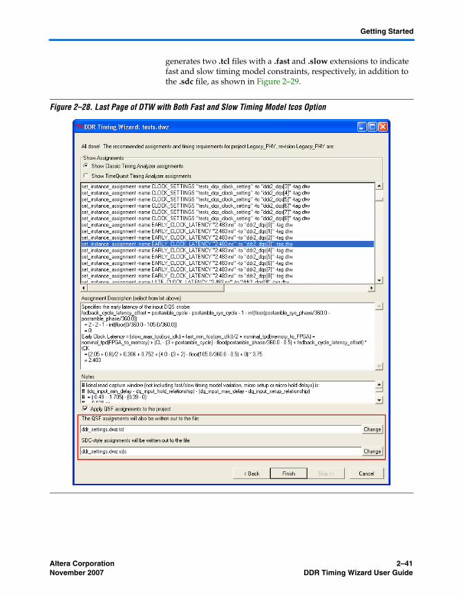
Getting Started
generates two .tcl files with a .fast and .slow extensions to indicate fast and slow timing model constraints, respectively, in addition to the .sdc file, as shown in Figure 2–29.
Figure 2–28. Last Page of DTW with Both Fast and Slow Timing Model tcos Option
Altera Corporation 2–41November 2007 DDR Timing Wizard User Guide
Entering and Editing Inputs to the DTW
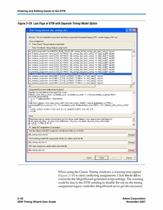
Figure 2–29. Last Page of DTW with Separate Timing Model Option
When using the Classic Timing Analyzer, a warning may appear (Figure 2–30) to alert conflicting assignments. Click Yes to All to overwrite the MegaWizard-generated script settings. The warning could be due to the DTW needing to disable the cut on the timing assignment legacy controller MegaWizard set to get the necessary
2–42 Altera CorporationDDR Timing Wizard User Guide November 2007

Getting Started
timing results from the Quartus II Classic Timing Analyzer. This message can also occur if you are updating some timing constrains from a previously-run DTW assignments. Figure 2–30 shows an example of conflicting assignment on the cut timing path.
Figure 2–30. The DTW Warning Window on Conflicting Assignments
The last page of DTW when using TimeQuest Timing Analyzer names is shown in Figure 2–31 on page 2–44.
Altera Corporation 2–43November 2007 DDR Timing Wizard User Guide

Entering and Editing Inputs to the DTW
Figure 2–31. Last Page of the DTW When Using TimeQuest Timing Analyzer
To change the output file name and location, type in the new file name and location, and click the Change button.
Click Finish.
2–44 Altera CorporationDDR Timing Wizard User Guide November 2007

Getting Started
After you click Finish, your project should have the following assignments:
● DQS/DQ pin location, loading, and I/O standard assignments from the legacy controller MegaWizard-generated script
● Timing constraints from the DTW
17. Add the additional assignments as listed on Step 4 of the “Design Flow” section.
You are now ready to compile the design and perform timing analysis.
The DTW Pages for QDRII+/QDRII SRAM & RLDRAM II
The steps for the QDRII+/QDRII SRAM or RLDRAM II interface are similar to the steps for the DDR/DDR2 SDRAM interface. The following is a summary:
1. From the Tools menu, select Tcl Scripts. Select DTW and click Run.
2. Specify a .dwz file name to save the timing constraints for the design and click Next.
3. Confirm the project directory and revision you want to use and click Next.
4. On the Import page, click Next, then click Next again.
5. Select the memory type and device and click Next.
6. Specify your CQ pins (for QDRII+/QDRII SRAM) or QK pins for (RLDRAM II) and click Next.
7. Specify the read data associated with each CQ and QK pins. For QDRII+/QDRII SRAM, you must specify the QK# pins if you are using it to capture data and click Next.
8. Specify the clocks to the memory and click Next.
9. Specify the write data and data mask pins associated with each write clock and click Next.
10. Specify control and address pins and click Next.
11. Specify PLL outputs driving the memory clocks and the resynchronization scheme and click Next.
Altera Corporation 2–45November 2007 DDR Timing Wizard User Guide
DTW Limitations
1 You can use a similar resynchronization scheme like DDR/DDR2 interfaces or use a FIFO to resynchronize the data back to the system clocks. Altera RLDRAM II and QDRII+/QDRII SRAM Controller MegaCore functions use a FIFO for data resynchronization.
12. Specify the PLL output generating the write clocks and click Next.
13. Enter board skew information and click Next.
14. Verify the FPGA parameters page and click Next.
1 You can either use the default numbers or tCOs if you have compiled the design.
1 All of the assignments made based on your inputs are available on the final page.
15. Confirm the final page and click Finish.
16. Add the additional assignments as listed on Step 4 of “Design Flow” on page 2–1.
17. Compile the design.
DTW Limitations Limitations when using the DTW include:
■ Proper timing analysis of outputs (such as write data, data masks, addresses, and commands) can only be performed with the TimeQuest Timing Analyzer using the Synopsys design constraints (SDC) file generated by the DTW. The SDC file is specified by the last line on the last panel of the DTW (see Figure 2–31 on page 2–44). However, even if you are using the classic timing analyzer, the dtw_timing_analysis.tcl script will use TimeQuest Timing Analyzer to analyze the timing of these outputs.
■ The SDC file currently only supports full-rate address/command timing.
■ If you are using a custom QDRII+ SRAM interface, add the QVLD pin as an additional read data pin. The current version of the Altera QDRII+ SRAM controller MegaCore function does not support QVLD pin.
2–46 Altera CorporationDDR Timing Wizard User Guide November 2007
Getting Started
■ When using the DDR/DDR2 SDRAM core version 3.4.0 and Quartus II version 6.0 or older with DQS hardware capture and a fedback clock, the read resynchronization to the System PLL cycle is imported from the IP, assuming it is normalized for a CAS 2 memory. It is actually normalized for a CAS 3 memory, so adjust the read resynchronization cycle by +1 on the PLL Parameters page (see Figure 2–19 on page 2–25).
■ When using the DDR/DDR2 SDRAM core version 3.4.0 with DQS hardware capture and a fedback clock, the DTW may make poor estimates for the first stage read resynchronization and postamble cycles in the PLL parameters page (Figure 2–19 on page 2–25). These may need to be adjusted to line up the timing analysis for the second stage read resynchronization and read postamble.
■ If you use the DQS hardware with the read postamble hardware, the transfer of the postamble signal from the system (0°) clock to the read postamble clock does not have an uncertainty assignment applied to it. Manually apply the same uncertainty used for the DQS to resynchronization clock transfer to the system clock to postamble clock transfer.
■ The Node browse buttons can take some time to respond if your design is a large one.
■ When using the Classic Timing Analyzer, the maximum data arrival skew assignments cannot be translated into PrimeTime timing assignments, as maximum data arrival skew is not a PrimeTime defined assignment. If using the TimeQuest Timing Analyzer, the output skew will be checked with set_output_delay constraints that can be translated to PrimeTime.
■ You can ignore similar warnings as below that may occur when updating timing netlist in TimeQuest:
Info: The source clock for this clock assignment cannot be reached. Clock: clk_to_sdram[0] might not have valid arrival time.
This is because TimeQuest tries to compute a generated clock’s (clk_to_sdram[0] signal in this example) clock latency by finding the base clock of the generated clock by tracing its inputs. In this case, the generated clock is the feedback clock input pin, which does not have any inputs to trace. The Info messages are noting this fact, and the fact that it will have to rely entirely on the set_clock_latency assignments on the feedback pin for its latency.
Altera Corporation 2–47November 2007 DDR Timing Wizard User Guide

DTW Limitations
2–48 Altera CorporationDDR Timing Wizard User Guide November 2007
Altera Corporation November 2007
3. Using thedtw_timing_analysis.tcl
Script
Introduction If your design does not meet timing, you must know how to optimize the design to meet all the timing requirements. DTW is a constraining tool; however, it does not actually perform timing analysis or offer suggestions on how to optimize the design.
The Quartus II compilation report lists the timing analysis results from the timing constraints applied by the DTW. These are shown as setup and hold margins on a per-pin basis for a given clock domain. You can use this information to optimize the design, but manual timing margin extraction and optimization is tedious as the optimization part requires iterative compilation and phase shift adjustments.
The dtw_timing_analysis.tcl script extracts the margin for every pin and displays the worst margin for each timing path with both fast and slow timing models, and suggests the best phase shift selections for the interface. This section describes how to use the dtw_timing_analysis.tcl script to perform the required timing analysis and optimize designs with memory interfaces.
3–1
Introduction
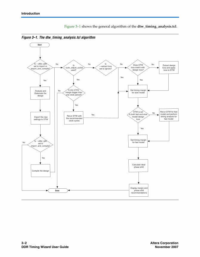
Figure 3–1 shows the general algorithm of the dtw_timing_analysis.tcl.
Figure 3–1. The dtw_timing_analysis.tcl algorithm
Extract design tcos and apply
tcos to DTW
Start
Yes
No
Done
Is —after_iptb set to import or
import_and_compile?
Is —auto_adjust_cycles
used?
Is —extract tcos set to Ignore?
Does DTW tcos match with
design tcos?
Is any of the margin bigger than one clock period?
DTW is set to both fast and slow
model design tcos
Analyze and Elaborate the
design
Import the new settings to DTW
Compile the design
Rerun DTW with the recommended
clock cycles
Get timing margin for slow model
Get timing margin for fast model
Calculate ideal phase shift
Display margin and phase shift
recommendations
Rerun DTW for fast model and perform timing analysis for
fast model
Is —after_iptb set to
import_and_compile?
YesYes
Yes
Yes
Yes
No No No
No
Yes
No
Yes
No
3–2 Altera CorporationDDR Timing Wizard User Guide November 2007
Using the dtw_timing_analysis.tcl Script
Running dtw_timing_analysis.tcl Script
To run DTW, complete the following steps:
1. Open a command prompt.
2. Change the directory in the command prompt to point to the project directory.
3. Run the dtw_timing_analysis.tcl script from the Quartus II installation directory. The command to call the script is as follows (provided that you have the default Quartus II installation directory and use DTW settings saved in the project directory called ddr_settings.dwz):
quartus_sh -t c:\altera\<version>\quartus\common\tcl\apps\gui\dtw\dtw_timing_analysis.tcl -dwz_file ddr_settings.dwz
Alternatively, you can copy the dtw_timing_analysis.tcl script from the c:\altera\<version>\quartus\common\tcl\apps\gui\dtw\ directory to your project directory and run it with the following command:
quartus_sh -t dtw_timing_analysis.tcl -dwz_file ddr_settings.dwz
The command listed in step 3 above is the minimum command that you need to type to run the dtw_timing_analysis.tcl script. The dtw_timing_analysis.tcl script has other switches that you can add when running the script, as listed in Table 3–1.
Table 3–1. Switches in the dtw_timing_analysis.tcl Script (Part 1 of 4) Notes (1), (2)
Switch Possible Value Description Required
-dwz_file <value> The .dwz file name Indicates which .dwz file is valid and to be analyzed. This is the only required field for the script.
Yes
-? or -help None Lists all the switches available for the script.
No
Altera Corporation 3–3November 2007 DDR Timing Wizard User Guide

Introduction
-after_iptb <value> import Instructs the script to analyze and elaborate the design and import the design settings into DTW. Use this switch after making changes in the PLL or memory controller MegaWizard. You must create a memory controller using the MegaWizard to use this switch. The default value for this switch is none, which means that the script does not import any settings.
No
import_and_compile Allows the script to compile the design, extract the timing margins, and recommend ideal clock cycles and phase shift settings after performing the import part of the script (see above).
No
-auto_adjust_cycles None Allows the script to adjust the clock cycles if the current absolute timing margin is bigger than one clock period. This is to set the design properly so that the margin shown is accurate and realistic. You have to add this switch if you want the script to adjust the clock cycles automatically. The correct clock cycle will updated the .dwz file automatically.
No
-extract_tcos <value> ● yes● no● auto● prompt
Indicates whether you want the script to extract the design tCOs and import them into DTW when the design tCOs do not match what are currently in DTW. The default setting is auto, which compares the tCOs and imports the design tCOs if they do not match the current DTW information. You can extract tCOs at every run (yes) or ignore the tCO mismatch (no). When the value is prompt, the script exits if the design tCOs do not match the DTW information. Extracting tCOs may take a while if you have a big design.
No
-debug None Lists debug messages. No
Table 3–1. Switches in the dtw_timing_analysis.tcl Script (Part 2 of 4) Notes (1), (2)
Switch Possible Value Description Required
3–4 Altera CorporationDDR Timing Wizard User Guide November 2007
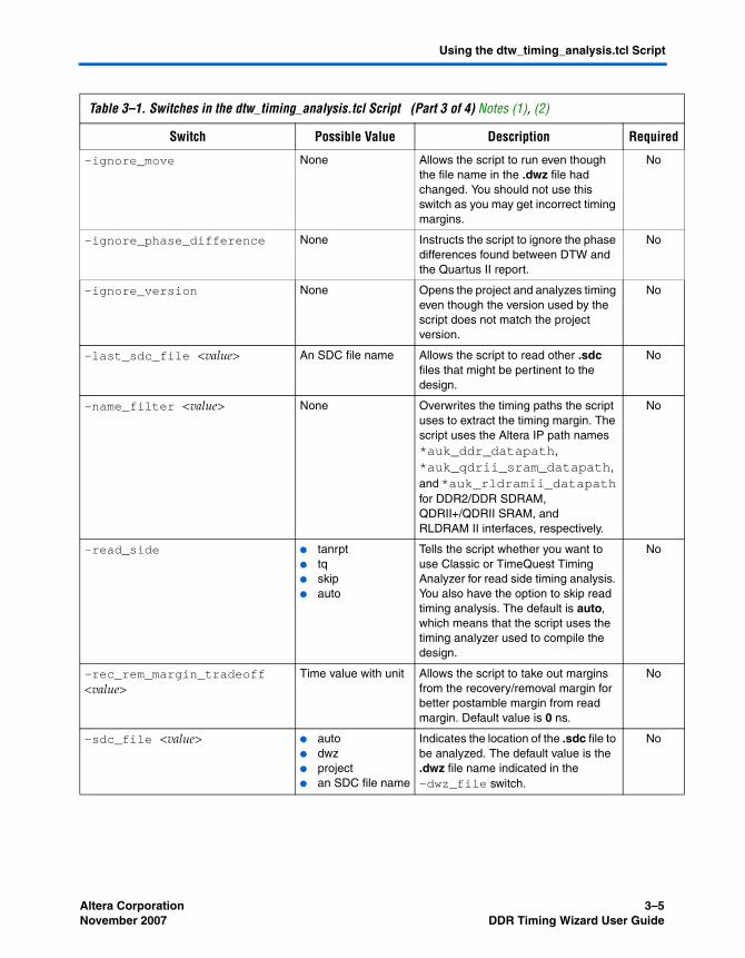
Using the dtw_timing_analysis.tcl Script
-ignore_move None Allows the script to run even though the file name in the .dwz file had changed. You should not use this switch as you may get incorrect timing margins.
No
-ignore_phase_difference None Instructs the script to ignore the phase differences found between DTW and the Quartus II report.
No
-ignore_version None Opens the project and analyzes timing even though the version used by the script does not match the project version.
No
-last_sdc_file <value> An SDC file name Allows the script to read other .sdc files that might be pertinent to the design.
No
-name_filter <value> None Overwrites the timing paths the script uses to extract the timing margin. The script uses the Altera IP path names *auk_ddr_datapath, *auk_qdrii_sram_datapath, and *auk_rldramii_datapath for DDR2/DDR SDRAM, QDRII+/QDRII SRAM, and RLDRAM II interfaces, respectively.
No
-read_side ● tanrpt● tq● skip● auto
Tells the script whether you want to use Classic or TimeQuest Timing Analyzer for read side timing analysis. You also have the option to skip read timing analysis. The default is auto, which means that the script uses the timing analyzer used to compile the design.
No
-rec_rem_margin_tradeoff <value>
Time value with unit Allows the script to take out margins from the recovery/removal margin for better postamble margin from read margin. Default value is 0 ns.
No
-sdc_file <value> ● auto ● dwz ● project ● an SDC file name
Indicates the location of the .sdc file to be analyzed. The default value is the .dwz file name indicated in the -dwz_file switch.
No
Table 3–1. Switches in the dtw_timing_analysis.tcl Script (Part 3 of 4) Notes (1), (2)
Switch Possible Value Description Required
Altera Corporation 3–5November 2007 DDR Timing Wizard User Guide

Introduction
4. Open the Compilation Report panel by clicking on Compilation Report under the Processing menu. If the Compilation Report panel is open, you have to close it and reopen it.
The dtw_timing_analysis.tcl script appends its result onto the Compilation Report, and is automatically displayed after refreshing the Compilation Report panel.
The dtw_timing_analysis.tcl Script Results
The script result is added at the bottom of the compilation result as Memory Interface Timing with the name of the controller and .dwz file in parentheses under that folder, and shows the script result with my_core (ddr_settings.dwz), because the controller’s name is my_core and the .dwz file name used to constrain the memory interface timing is called ddr_settings.dwz, as shown in Figure 3–2.
-stop_after <value> Any integer Indicates the maximum number of iterations when using the -auto_adjust_cycles switch to prevent infinite iterations. The default value is 5.
No
-vwf_file_name <value> A .vwf file name Creates a waveform showing the interface timing margin in a .vwf format.
No
-write_side ● tanrpt● tq● skip● auto
Tells the script whether you want to use Classic or TimeQuest Timing Analyzer for the write side timing analysis. You also have the option to skip write timing analysis. The default is TimeQuest Timing Analyzer, regardless of what timing analyzer was used in the design. Classic timing analyzer is not recommended for write timing analysis.
No
Notes to Table 3–1:(1) Fedback clock in this implementation is used for read capture, not for resynchronization.(2) RLDRAM II and QDRII+/QDRII SRAM interfaces do not require resynchronization clocks, as the Altera IP MegaCore
functions use a FIFO to resynchronize data to system clock.
Table 3–1. Switches in the dtw_timing_analysis.tcl Script (Part 4 of 4) Notes (1), (2)
Switch Possible Value Description Required
3–6 Altera CorporationDDR Timing Wizard User Guide November 2007

Using the dtw_timing_analysis.tcl Script
Figure 3–2. Script Results as Part of Timing Analyzer Results
Each .dwz file folder under Memory Interface Timing has three panels:
■ Timing Summary
Figure 3–3 shows an example of the Timing Summary panel.
Figure 3–3. Example Design Timing Summary
This panel shows current and ideal margins for each timing path for the interface. Current margin is the smallest margin of the path calculated from the setup and hold timing margins for both fast and slow timing models (also shown in this panel). The current margin shows how much delay you can shift either to the right or left of the current shift before timing breaks the design requirements.
1 When the design uses slow timing model tcos only, the script automatically runs fast timing model timing analysis to get the fast timing model timing margin.
Table 3–2 shows the paths that are analyzed for the different memory interface implementations.
Altera Corporation 3–7November 2007 DDR Timing Wizard User Guide

Introduction
f For more information on the different implementations available in Stratix II, Stratix II GX and Arria GX devices, refer to AN328: Interfacing DDR2 SDRAM in Stratix II, Stratix II GX, and Arria GX Devices.
Ideal margin is calculated by adding the smallest setup and smallest hold time margin between the fast and slow timing models and dividing the total by two to show a balanced setup and hold margin, as shown in the following equation:
Ideal margin = (smallest setup margin + smallest hold margin)/2
Table 3–2. Memory Interface Paths Analyzed by the Script
DDR2/DDR SDRAM
(DQS mode)
DDR2/DDR SDRAM
(non-DQS mode)
QDRII+/QDRII SRAM and RLDRAMII (DQS and non-DQS mode)
Description
Fedback PLL
One PLL
Fedback PLL
One PLL
Read Capture v v v v v Margin at the read capture registers
Fedback Clock v N/A (1) N/A N/A Margin at the resynchronization registers clocked by the fedback PLL output
Resynchronization Clock
v v v (2) (3) Margin at the resynchronization registers clocked by the system PLL output
Recovery/Removal v v N/A N/A N/A Margin for the DQS postamble registers
Postamble v (2) N/A N/A N/A Margin for the registers, clocked by the system clock, whose output goes to the postamble registers
tDQSS v v v v N/A Margin for skew relationship between CK and DQS signals
Write Capture v v v v v Margin for write data
Address/Command v v v v v Margin for address and command
Notes to Table 3–2:(1) Fedback clock in this implementation is used for read capture, not for resynchronization. The script analyzes this
as read capture.(2) Quartus II software reports the margin because this path is a clock domain transfer between two outputs of the
same PLLs.(3) RLDRAM II and QDRII+/QDRII SRAM interfaces do not require resynchronization clocks as the Altera IP
MegaCores use a FIFO to resynchronize data to the system clock.
3–8 Altera CorporationDDR Timing Wizard User Guide November 2007

Using the dtw_timing_analysis.tcl Script
The PLL name column shows which PLL clock tap is used for the path.
■ Recommended Settings
This panel shows the current and new clock cycle and phase shift selections for the interface. The current shift and clock cycle show what are currently set in the DTW. The new shift and clock cycle are calculated by the dtw_timing_analysis.tcl script as the recommended settings. Only read side paths have clock cycle selections. You should follow the clock cycle and phase shift selection suggested in the Recommended Settings whenever possible for the most optimal settings for the design.
The new phase shifts shown are the ideal phase shift to achieve balanced setup and hold margin. However, note that the PLL may not be able to achieve that particular phase shift. If the current phase shift and the new phase shift differs by less than 15°, your design already uses the optimal settings.
Figure 3–4 shows an example of the Recommended Settings panel.
Figure 3–4. Example Design Recommended Settings
The PLL name column shows which PLL clock tap is used for the path. Note that the same PLL output tap may be used for multiple paths, so be careful when changing the phase shift on this PLL output as it will change the margin on the other tap.
Altera Corporation 3–9November 2007 DDR Timing Wizard User Guide

Introduction
art 1
clk0
]
Table 3–3 shows the default clock names and usage if you are using the Altera DDR2 SDRAM Controller MegaCore function.
Table 3–3. Default Clock Names and Usage in Altera DDR2 SDRAM Controller MegaCore Function Note (1) (Pof 2)
Clock Usage Timing Analyzer Clock Name
System clock Classic Timing Analyzer
*:g_stratixpll_ddr_pll_inst|altpll:altpll_component|_clk0
TimeQuest Timing Analyzer
*g_stratixpll_ddr_pll_inst|altpll_component|pllclk[0]
Write clock Classic Timing Analyzer
*:g_stratixpll_ddr_pll_inst|altpll:altpll_component|_clk1
TimeQuest Timing Analyzer
*g_stratixpll_ddr_pll_inst|altpll_component|pllclk[1]
Second resynchronization clock
Classic Timing Analyzer
*:g_stratixpll_ddr_pll_inst|altpll:altpll_component|_clk2
TimeQuest Timing Analyzer
*g_stratixpll_ddr_pll_inst|altpll_component|pllclk[2]
CK/CK# (when using dedicated clock output pins)
Classic Timing Analyzer
*:g_stratixpll_ddr_pll_inst|altpll:altpll_component|_clk3
TimeQuest Timing Analyzer
*g_stratixpll_ddr_pll_inst|altpll_component|pllclk[3]
First resynchronization clock
Classic Timing Analyzer
*:g_stratixpll_ddr_fedbackpll_inst|altpll:altpll_component|_
TimeQuest Timing Analyzer
*g_stratixpll_ddr_fedback_pll_inst|altpll_component|pllclk[0
3–10 Altera CorporationDDR Timing Wizard User Guide November 2007

Using the dtw_timing_analysis.tcl Script
clk1
]
II t not
art 2
When you must change a PLL output phase shift that will affect another path adversely, create another PLL output tap instead. This requires manual RTL changes and editing the PLL clock usage.
Table 3–4 shows the path recommended by the script for the different memory interfaces.
Typically, the write timing paths use a variation of the system or the write clock. Table 3–4 shows some variations of the available clocks that the Altera DDR2 SDRAM Controller MegaCore function may use.
You can use information from Table 3–4 to achieve 0°, 90°, 180°, or 270° in your design. However, if the phase shift required is not one of the four options, you may need to add a dedicated PLL output and change the clock connections for these paths to achieve the best margin. For interfaces above 200 MHz, Altera recommends to always use a dedicated PLL output.
Dedicated postamble clock
Classic Timing Analyzer
*:g_stratixpll_ddr_fedbackpll_inst|altpll:altpll_component|_
TimeQuest Timing Analyzer
*g_stratixpll_ddr_fedback_pll_inst|altpll_component|pllclk[1
Note to Table 3–3:(1) System clock and write clock defaults to 0° and -90° phase shift, respectively, in DDR2/DDR SDRAM and RLDRAM
memory interfaces. In QDRII+/QDRII SRAM interfaces, the system clock is 0°, but the write clock is at 90°. You muschange the phase shift of these clocks, as it will affect the whole system.
Table 3–3. Default Clock Names and Usage in Altera DDR2 SDRAM Controller MegaCore Function Note (1) (Pof 2)
Clock Usage Timing Analyzer Clock Name
Table 3–4. Available Phase Shifts without Extra Dedicated PLL Outputs
Clock Usage Variation Phase Shift Achieved
System clock Rising edge 0°
System clock Falling edge 180°
Write clock Rising edge –90° or 270°
Write clock Falling edge 90°
Altera Corporation 3–11November 2007 DDR Timing Wizard User Guide

Timing Closure Process
■ What To Do Next
This panel shows how to proceed in the design. If clock cycles need changing, this panel details the necessary steps required before moving on to fixing the phase shifts.
Figure 3–5 shows an example of the What To Do Next panel.
Figure 3–5. What To Do Next Panel
Remember to check the PLL output counter for each clock before changing any phase shift. You should not change PLL output clocks c0 (system clock) and c1 (write clock) as changing phase shift for these clock will affect the memory controllers. Furthermore, PLL output clock c0 may change the timing for the entire system since it can be used as a system clock for the entire design. Instead, find out if you can use a different PLL clock output instead to meet timing on that particular path.
Timing Closure Process
This section describes different situations that you may encounter in your timing closure process. Most of the sub-sections below fall in the Adjust Constraints step of the memory interfaces design flow.
Figure 3–6 shows the timing closure process. You need to resynthesize the design if you make any changes in the RTL files or MegaWizard GUI to ensure that DTW is able to import the new settings. You can do so manually or use the –import or –import_and_compile switch in the dtw_timing_analysis.tcl script.
3–12 Altera CorporationDDR Timing Wizard User Guide November 2007

Using the dtw_timing_analysis.tcl Script
Figure 3–6. Timing Closure Process
Note to Figure 3–6:(1) Depending on your design, you may need to change the RTL even after changing the clock cycle and phase shift of
the data path.
No
Compile Design
Run dtw_timing_analysis.tcl
Is the Memory InterfaceTiming Met?
Change RTL (1)
Change Phase Shift inaltpll MegaWizard
Update Clock Cycleand/or Phase Shift
in the Legacy ControllerMegawizard
Update DTW-OnlySettings
Perform Analysis &Synthesis
Re-Import Settings to DTW
End
Yes
Altera Corporation 3–13November 2007 DDR Timing Wizard User Guide

Timing Closure Process
Timing Closure Differences in DDR2/DDR SDRAM, QDRII+/QDRII SRAM, and RLDRAM II Interfaces
Of the three legacy memory controllers, DDR2/DDR SDRAM controllers have the most options or settings that you can change. These controllers are also the ones that have a more complicated timing closure process, especially when running at high speeds.
DDR2/DDR SDRAM Interfaces
You can make changes to the DDR2/DDR SDRAM controller settings four different ways:
■ In the DDR2/DDR SDRAM MegaWizard■ In the altpll MegaWizard■ In the RTL files■ In the DTW directly
These changes are described in more detail in the later sections.
QDRII+/QDRII SRAM Interfaces
QDRII+/QDRII SRAM interfaces only uses two clocks: a system clock and write clock, which already have default phase shifts. The address/command clock defaults to the inverted write clock and cannot be changed. Furthermore, QDRII+/QDRII SRAM uses a FIFO to resynchronize the data to the system clock domain, so you do not need to provide a resynchronization clock.
To constrain the timing between the read data and the resynchronization registers, use the setup_relationship and hold_relationship constraints when using Classic Timing Analyzer. For designs using TimeQuest Timing Analyzer, convert the setup_relationship and hold_relationship constraints to SDC constraints manually. The setup_relationship and hold_relationship assignment can be directly converted to set_max_delay and set_min_delay assignments, as shown in the following example:
set_max_delay -0.2 -from * -to <resync registers*> set_min_delay -1.6 -from * -to <resync registers*>
3–14 Altera CorporationDDR Timing Wizard User Guide November 2007

Using the dtw_timing_analysis.tcl Script
RLDRAM II Interfaces
In RLDRAM II interfaces, the only PLL phase shift that you can change using the MegaWizard is for the address/command clock connection phase shift (see Figure 3–7) . You can also change the address/command clock connection directly in the RTL, and its phase shift using the altpll MegaWizard.
RLDRAM II interfaces uses two other clocks: system clock and write clock, which have default phase shifts.
Figure 3–7. RLDRAM II MegaWizard Timing Panel
Altera Corporation 3–15November 2007 DDR Timing Wizard User Guide

Timing Closure Process
For RLDRAM II designs created in Quartus II version 7.2 and higher, add the Megawizard-generated <variation_name>_controller.sdc file. This .sdc file defines false paths between the QK signals and the PLL clock output c0 used to read from the FIFO.
1 If the PLL clock output names used in the design are different from the names defined in the MegaWizard-generated .sdc file, the false path constraints are ignored. Change the PLL clock name with the one reported in TimeQuest Timing Analyzer and re-analyze timing again. You can check whether any constraints are ignored by double-clicking on the Ignored Constraints section in the TimeQuest Timing Analyzer.
Selecting Initial Phase Shifts
Memory interfaces with 2-PLL implementation have the most PLL clock output usage. Furthermore, this implementation supports the highest performance, so it is typically designs with 2-PLL memory interfaces that have the most complexity to meet timing.
When using 1-PLL mode, you can use the resynchronization and postamble clock cycles and phase shifts suggested by the legacy controller MegaWizard as your starting point. In 2-PLL mode, however, the legacy controller MegaWizard does not recommend any phase shifts for the resynchronization or postamble clocks. In this case, you can use 0° phase shift for both resynchronization clocks and 90° phase shift for the postamble clock, as shown in Figures 3–8, as your starting point. Choose these settings when instantiating the PHY for the first time.
3–16 Altera CorporationDDR Timing Wizard User Guide November 2007
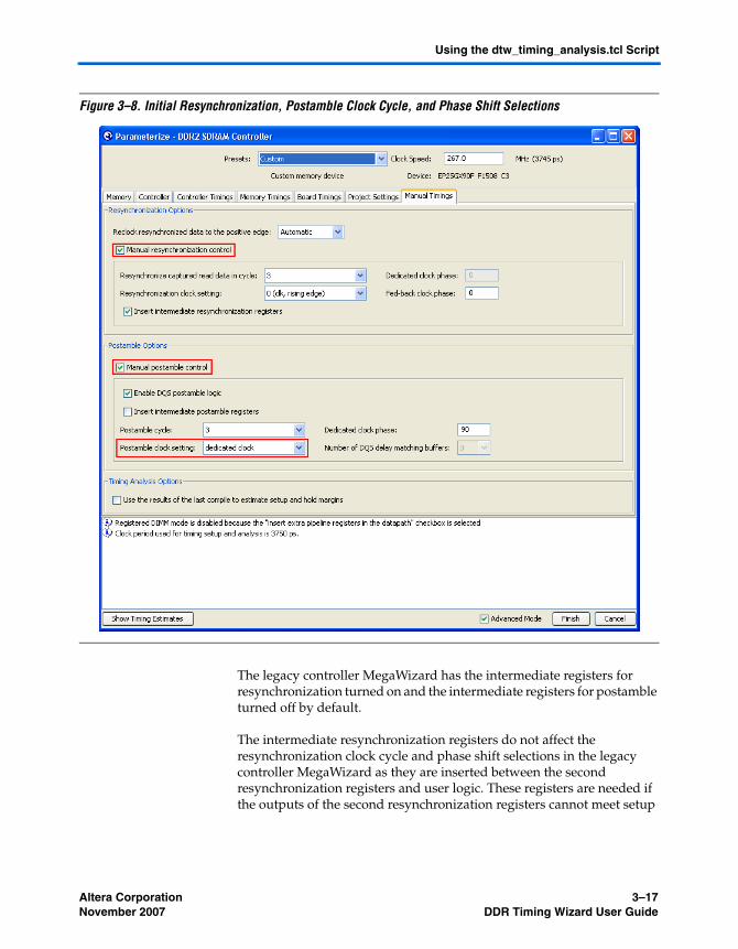
Using the dtw_timing_analysis.tcl Script
Figure 3–8. Initial Resynchronization, Postamble Clock Cycle, and Phase Shift Selections
The legacy controller MegaWizard has the intermediate registers for resynchronization turned on and the intermediate registers for postamble turned off by default.
The intermediate resynchronization registers do not affect the resynchronization clock cycle and phase shift selections in the legacy controller MegaWizard as they are inserted between the second resynchronization registers and user logic. These registers are needed if the outputs of the second resynchronization registers cannot meet setup
Altera Corporation 3–17November 2007 DDR Timing Wizard User Guide

Timing Closure Process
and hold time requirements of the user logic clocked by the system clock. The ideal phase shift may change by a few degrees, due to place-and-route changes due to the register insertion.
The intermediate postamble registers, on the other hand, affects the postamble clock cycle and phase shift selections. When the Intermediate postamble registers option is unchecked, the clock going to the system postamble registers is the system clock inverted by 180°. When that option is checked, the clock going to the system postamble registers is the 0° system clock. Therefore, the state of this option affects the clock phase shift of the dq_enable_reset registers.
Figures 3–9 shows the relationships of the resynchronization registers and postamble registers with their respective intermediate registers for fedback-PLL mode interfaces in Stratix II devices. The name of the registers shown are from the DDR2 SDRAM Controller Compiler names.
Figure 3–9. Resynchronization, Postamble, and Intermediate Registers Connections for Fedback-PLL mode in Stratix II Devices
Re-run DTW After First Compile When Using Classic Timing Analyzer
For any memory interfaces using Classic Timing Analyzer, you need to extract the design tCO to the DTW after the first compile and then run the dtw_timing_analysis.tcl script. To extract tCOs, you can either use the
D Q
Fedback PLL
D Q D Q D Q
D Q
D QSystem PLL
Q D Q DQ D
dq_capture resynched_datafedback_
resynched_datainter_rdata
User logic
dq_enable_reset doing_rd_delayed
dq
dqs
DQ
DQS, CK/CK#, Address,
Command, Fedback out
User logic
Optional, depending on setting of "Insert intermediate
resynchronization registers"
Optional, depending on setting of "Insert intermediate postamble registers"
Fedback clock in
Optional Fedback clock out
Optional CK/CK#
clk1
clk0
clk2clk0
clk3
clk1
First Resynchronization
Registers
Second Resynchronization
Registers
Intermediate Resynchronization
Registers
Postamble System Postamble
3–18 Altera CorporationDDR Timing Wizard User Guide November 2007
Using the dtw_timing_analysis.tcl Script
Extract tcos button in DTW or use the –extract_tco switch in the dtw_timing_analysis.tcl. You need to extract the CK/CK# tCOs manually if you are using dedicated clock output for CK/CK# (as in designs targeting HardCopy II devices). Also, if you did not lock down your pins, your design's tCOs may vary from one compilation to another. These tCO
numbers are used to calculate skew between output pins for your write timing margin.
1 You do not need this step when using TimeQuest Timing Analyzer as TimeQuest Timing Analyzer does not use skew to calculate write timing margin. Instead, it uses set_output_delay assignments.
Ensure the Changes Made Outside Legacy Controller MegaWizard Are Not Erased When the Core is Regenerated
This is applicable to DDR2/DDR SDRAM, QDRII+/QDRII SRAM, and RLDRAM II interfaces.
When you click Generate in the legacy controller MegaWizard, all RTL and constraint files are regenerated. If you have made any changes to the constraints or RTL files outside of the MegaWizard, these changes may be reverted back to the initial MegaWizard settings. You can avoid this by disabling some of the Project Settings options.
There are four options that you can set under the Example Design Settings in the legacy DDR2/DDR SDRAM controller MegaWizard:
1 There are only three options available in the legacy QDRII+/QDR II SRAM and RLDRAM II controller MegaWizard. These memory controllers do not have their own timing analysis script.
1. Automatically apply datapath-specific constraints to the Quartus II project.
This setting runs the auto_add_ddr_constraints.tcl before the design compilation. You should disable this if you are making any changes to a compiled project where you had made changes to the constraints to suit your actual board layout.
2. Update the example design file that instantiates the controller variation.
This setting updates the design example connections, if you had made changes to the resynchronization or postamble connection. However, if you had changed the RTL files previously to create a
Altera Corporation 3–19November 2007 DDR Timing Wizard User Guide

Timing Closure Process
dedicated PLL output for your address/command clock or to add your own logic to the example design, disable this option so that the MegaWizard does not overwrite your previous changes. If you change any clock connections in the MegaWizard (such as the postamble and resynchronization clock connections), you must manually change the connection in the RTL files.
3. Automatically verify datapath-specific timing in the Quartus II project.
This setting runs the verify_timing.tcl script that the MegaWizard generates to check the timing of the interface. However, you should use DTW to close timing. This setting needs to be disabled when you generate the memory controller for the first time. This option is not available in the QDRII+/QDRII SRAM and RLDRAM II memory interfaces.
4. Update the example design PLL.
This setting updates any phase shift changes for the PLLs. Disable this option if you had created a dedicated PLL output for your address/command clock, or if you had added other PLL output clocks for other parts of your design. You then need to manually change the phase shift in the altpll MegaWizard.
1 In a 2-PLL mode interface, the fedback PLL always gets updated even with this option off. This option only disables PLL changes for the system PLL in these interfaces.
Figure 3–10 shows a modified Project Settings window where all four settings are disabled. With these options off, any changes for timing closure can be done manually in the RTL or altpll MegaWizard, except:
● When you need to change the clock cycles of the resynchronization or postamble clock.
● When you need to add or remove the intermediate registers for the resynchronization or postamble path.
● When you need to add a dedicated clock for resynchronization, postamble, or the address/command clock (if you have not previously done so).
3–20 Altera CorporationDDR Timing Wizard User Guide November 2007
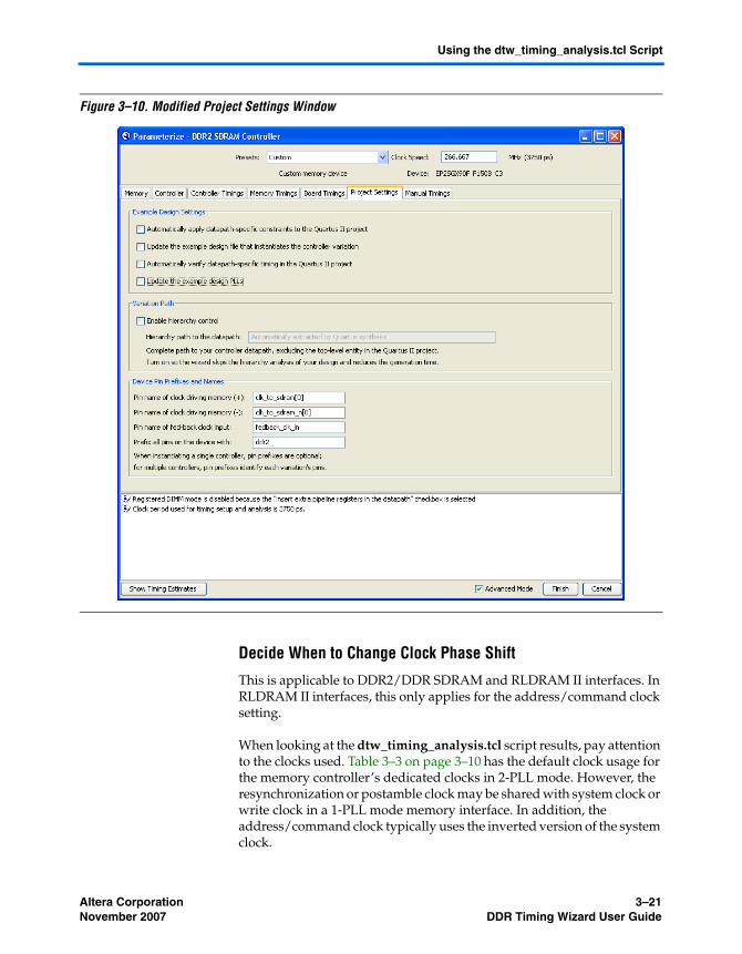
Using the dtw_timing_analysis.tcl Script
Figure 3–10. Modified Project Settings Window
Decide When to Change Clock Phase Shift
This is applicable to DDR2/DDR SDRAM and RLDRAM II interfaces. In RLDRAM II interfaces, this only applies for the address/command clock setting.
When looking at the dtw_timing_analysis.tcl script results, pay attention to the clocks used. Table 3–3 on page 3–10 has the default clock usage for the memory controller’s dedicated clocks in 2-PLL mode. However, the resynchronization or postamble clock may be shared with system clock or write clock in a 1-PLL mode memory interface. In addition, the address/command clock typically uses the inverted version of the system clock.
Altera Corporation 3–21November 2007 DDR Timing Wizard User Guide
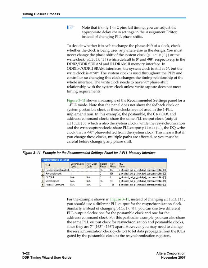
Timing Closure Process
1 Note that if only 1 or 2 pins fail timing, you can adjust the appropriate delay chain settings in the Assignment Editor, instead of changing PLL phase shifts.
To decide whether it is safe to change the phase shift of a clock, check whether the clock is being used anywhere else in the design. You must never change the phase shift of the system clock (pllclk[0]) or the write clock (pllclk[1]) which default to 0° and -90°, respectively, in the DDR2/DDR SDRAM and RLDRAM II memory interface. In QDRII+/QDRII SRAM interfaces, the system clock is still at 0°, but the write clock is at 90°. The system clock is used throughout the PHY and controller, so changing this clock changes the timing relationship of the whole interface. The write clock needs to have 90° phase-shift relationship with the system clock unless write capture does not meet timing requirements.
Figure 3–11 shows an example of the Recommended Settings panel for a 1-PLL mode. Note that the panel does not show the fedback clock or system postamble clock as these clocks are not used in the 1-PLL implementation. In this example, the postamble, the CK/CK#, and address/command clocks share the same PLL output clock (output pllclk[0] which is also the system clock), while the resynchronization and the write capture clocks share PLL output pllclk[1], the DQ write clock that is -90° phase-shifted from the system clock. This means that if you change these clocks, multiple paths are affected, so you must be careful before changing any phase shift.
Figure 3–11. Example for the Recommended Settings Panel for 1-PLL Memory Interface
For the example shown in Figure 3–11, instead of changing pllclk[1], you should use a different PLL output for the resynchronization clock. Similarly, instead of changing pllclk[0], you can use two different PLL output clocks: one for the postamble clock and one for the address/command clock. For this particular example, you can also share the same PLL output clock for resynchronization and postamble clocks, since they are 7° (163° - 156°) apart. However, you may need to change the resynchronization clock cycle to 2 to let data propagate from the IOEs gated by the postamble clock to the resynchronization registers.
3–22 Altera CorporationDDR Timing Wizard User Guide November 2007
Using the dtw_timing_analysis.tcl Script
For actual steps on how to change the phase shift, refer to “Changing Clock Phase Shift”.
Changing Clock Phase Shift
This is applicable to DDR2/DDR SDRAM interfaces and RLDRAM II interfaces. In RLDRAM II interfaces, this only applies for the address/command clock setting.
After making sure that it is safe to change the clock phase shift for a particular PLL output, you have two options to perform the change:
1. Via the Legacy Controller MegaWizard
To change the resynchronization and postamble clock phase shifts in DDR2/DDR SDRAM interfaces, go to the Manual Timings page of the DDR2/DDR SDRAM Parameterize window.
To change the address/command clock phase shift in RLDRAM II interfaces, go to the Timing page of the RLDRAM II Parameterize window. You can choose either the falling or rising edge of the system clock, write clock, or a dedicated PLL output clock. You can also pick any phase shift when using the dedicated PLL output clock for the address/command clock.
2. Via the altpll MegaWizard
In DDR2/DDR SDRAM interfaces, if you do not need to change the resynchronization or postamble or both clock cycles and you already used dedicated PLL output for these clocks, you can simply change the phase shift using the altpll MegaWizard for the PLL clock output to be adjusted.
In RLDRAM II interfaces, peform the following:
a. Determine which clock (system, write, or dedicated clock) you need for this path.
If the Recommended Settings panel from the dtw_timing_analysis.tcl asks you to use a phase shift that is closed to 0° or 180° clock, you can use the system clock with positive and negative edge, respectively. Similarly if it asks you to use a phase shift that is closed to 90° or 270° clock, use the write clock, with either negative or positive edge, respectively. If the phase shift recommended is not near to any of these phase shift, you need a dedicated PLL output clock.
Altera Corporation 3–23November 2007 DDR Timing Wizard User Guide

Timing Closure Process
b. Open the <project_name>.v/.vhd to check which clock is currently used.
c. Look for the line:
assign addr_cmd_clk =
If the text on the right-hand side of the "=" sign is either clk or write_clk, currently the address/command clock is using the system clock or write clock, respectively. You can change it to !clk or !write_clk, if you need the negative-edge version of the clock. If you need to use a dedicated PLL output clock instead, change that text to a different name (for example, dedicated_addr_cmd_clk).
1 Remember whether you selected the rising edge or the falling edge for the address/command active clock edge.
If you are using a dedicated PLL output clock:
i. Search for the following line in the <project_name>.v/.vhd:
rldramii_pll_stratixii
This is the PLL module for the RLDRAM II interface. You should see code similar to:
rldramii_pll_stratixii g_stratixii_pll_rldramii_pll_inst(.areset (reset),.c0 (clk),.c1 (write_clk),.c2 (addr_cmd_clk),.c3 (memory_clk_0),.c4 (memory_clk_1),.c5 (memory_clk_2),.inclk0 (clock_source),.locked (pll_locked));
Ensure that the c2 output is connected to dedicated_addr_ddr_cmd_clk.
3–24 Altera CorporationDDR Timing Wizard User Guide November 2007

Using the dtw_timing_analysis.tcl Script
ii. Open the altpll MegaWizard to modify the rldramii_pll_stratixii.v/.vhd and change the clock phase shift of the c2 output clock accordingly.
The altpll may not be able to give you the exact phase shift due to the PLL configuration, but it will give you the closest phase shift to the one that you set in either MegaWizard.
1 Whenever you make a change in the MegaWizard or the RTL files, peform an Analysis and Synthesis on the design before reimporting the settings into DTW.
Adjusting Clock Cycle Selections
A timing margin (either positive or negative) of more than one clock period in the Timing Summary panel indicates that one of the clock cycle selections in the DTW is incorrect. However, it does not necessarily mean that you need to change the clock cycle of this particular clock listed in the Timing Summary panel. The dtw_timing_analysis.tcl script analyzes the timing of the whole interface and may find that you need to adjust the clock cycle of the clock downstream from the clock listed in the Timing Summary panel.
For example, Figures 3–12 shows a current margin of -3.303 ns for the fedback clock for a 267-MHz DDR2 SDRAM design. However, if you look under the Slow Hold column, the fedback clock has a positive margin of 4.218 ns. This indicates that the clock arrives one clock cycle too late. In Figures 3–13, dtw_timing_analysis.tcl suggests that you need to add one clock cycle to the resynchronization clock, and not the fedback clock.
Figure 3–12. Timing Summary Example with <1 Clock Cycle Margin
Altera Corporation 3–25November 2007 DDR Timing Wizard User Guide
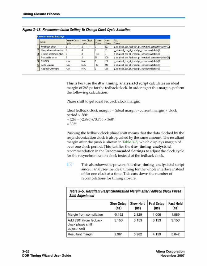
Timing Closure Process
Figure 3–13. Recommendation Setting To Change Clock Cycle Selection
This is because the dtw_timing_analysis.tcl script calculates an ideal margin of 263 ps for the fedback clock. In order to get this margin, peform the following calculation:
Phase shift to get ideal fedback clock margin:
Ideal fedback clock margin = (ideal margin - current margin)/ clock period × 360°= (263 - (-2.890))/3.750 × 360°= 303°
Pushing the fedback clock phase shift means that the data clocked by the resynchronization clock is also pushed by the same amount. The resultant margin after the push is shown in Table 3–5, which displays margin of over one clock period. This justifies the dtw_timing_analysis.tcl recommendation in the Recommended Settings to adjust the clock cycle for the resynchronization clock instead of the fedback clock.
1 This also shows the power of the dtw_timing_analysis.tcl script since it analyzes the ideal timing for the whole interface instead of for one clock at a time. This cuts down the number of recompilations for timing closure.
Table 3–5. Resultant Resynchronization Margin after Fedback Clock Phase Shift Adjustment
Slow Setup (ns)
Slow Hold (ns)
Fast Setup (ns)
Fast Hold (ns)
Margin from compilation -0.192 2.829 1.006 1.889
Add 330° (from fedback clock phase shift adjustment)
3.153 3.153 3.153 3.153
Resultant margin 2.961 5.982 4.159 5.042
3–26 Altera CorporationDDR Timing Wizard User Guide November 2007
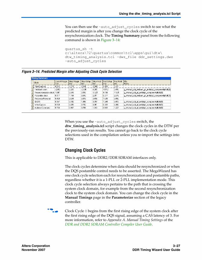
Using the dtw_timing_analysis.tcl Script
You can then use the -auto_adjust_cycles switch to see what the predicted margin is after you change the clock cycle of the resynchronization clock. The Timing Summary panel from the following command is shown in Figure 3–14:
quartus_sh -t c:\altera\72\quartus\common\tcl\apps\gui\dtw\dtw_timing_analysis.tcl -dwz_file ddr_settings.dwz -auto_adjust_cycles
Figure 3–14. Predicted Margin after Adjusting Clock Cycle Selection
When you use the -auto_adjust_cycles switch, the dtw_timing_analysis.tcl script changes the clock cycles in the DTW per the previously-ran results. You cannot go back to the clock cycle selections used in the compilation unless you re-import the settings into DTW.
Changing Clock Cycles
This is applicable to DDR2/DDR SDRAM interfaces only.
The clock cycles determine when data should be resynchronized or when the DQS postamble control needs to be asserted. The MegaWizard has one clock cycle selection each for resynchronization and postamble paths, regardless whether it is a 1-PLL or 2-PLL implementation mode. This clock cycle selection always pertains to the path that is crossing the system clock domain, for example from the second resynchronization clock to the system clock domain. You can change the clock cycle in the Manual Timings page in the Parameterize section of the legacy controller.
f Clock Cycle 0 begins from the first rising edge of the system clock after the first rising edge of the DQS signal, assuming a CAS latency of 3. For more information, refer to Appendix A. Manual Timing Settings of the DDR and DDR2 SDRAM Controller Compiler User Guide.
Altera Corporation 3–27November 2007 DDR Timing Wizard User Guide

Timing Closure Process
In the DTW, however, if you create a 2-PLL mode memory interface, DTW needs two clock cycle selections each for resynchronization and postamble paths. DTW uses the clock cycle selections from the legacy controller MegaWizard for one and estimates the clock cycles for the other one. See Figure 2–21 on page 29 and figure Figure 2–23 on page 33 for the relationship of the clock cycles in the legacy memory controller MegaWizard and the DTW.
Because of this relationship, depending on which clock cycle the dtw_timing_analysis.tcl asks you to adjust, you need to either change the clock cycle in the legacy memory controller MegaWizard or in the DTW. If the Recommended Settings panel asks you to change the clock cycle in both MegaWizard and DTW, change the clock cycle in DTW, synthesize the design, and re-import the memory settings into the DTW. More often than not, DTW will be able to recalculate the other clock cycle selection and pick the correct one. You should, however, ensure that they are correct.
Changing the Address/Command Clock Connection and Phase Shift
This is applicable to DDR2/DDR SDRAM interfaces only. To change the address/command clock in RLDRAM II interfaces, refer to the “Changing Clock Phase Shift” on page 3–23.
In order to use a dedicated PLL output clock for the address/command clock, you need to enable the Insert extra pipeline registers in the datapath option and disable the Clock address/command output registers on the negative edge option, as shown in Figure 3–15.
3–28 Altera CorporationDDR Timing Wizard User Guide November 2007
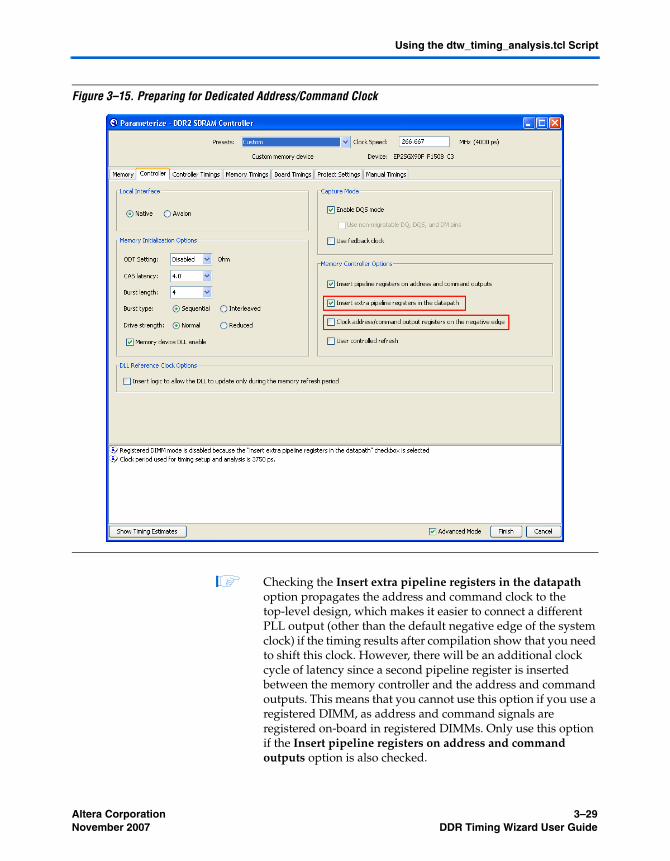
Using the dtw_timing_analysis.tcl Script
Figure 3–15. Preparing for Dedicated Address/Command Clock
1 Checking the Insert extra pipeline registers in the datapath option propagates the address and command clock to the top-level design, which makes it easier to connect a different PLL output (other than the default negative edge of the system clock) if the timing results after compilation show that you need to shift this clock. However, there will be an additional clock cycle of latency since a second pipeline register is inserted between the memory controller and the address and command outputs. This means that you cannot use this option if you use a registered DIMM, as address and command signals are registered on-board in registered DIMMs. Only use this option if the Insert pipeline registers on address and command outputs option is also checked.
Altera Corporation 3–29November 2007 DDR Timing Wizard User Guide
Timing Closure Process
1 The MegaWizard inverts the address/command clock in a lower-level file of the controller when the Clock address/command output registers on the negative edge option is on. Instead, you can manually add 180° phase shift in the altpll MegaWizard for easier tracking.
To use a dedicated PLL output for the address and command clock, enable the c3 output of the system PLL and connect this output to addrcmd_clk in the <variation_name> instantiation. The system PLL instantiation code in the <project_name>.v/vhd file looks similar to the example below:
ddr_pll_stratixii g_stratixpll_ddr_pll_inst(.c0 (clk),.c1 (write_clk),.c2 (dedicated_resynch_or_capture_clk),.c3 (dedicated_addrcmd_clk),.inclk0 (clock_source));
The MegaWizard uses an input PLL clock that is of the same frequency as the memory interface. You need to change this in the altpll MegaWizard for the ddr_pll_stratixii module.
In the <variation_name> instantiation in the <project_name>.v/file, change:
.addrcmd_clk (clk),
to:
.addrcmd_clk (dedicated_addrcmd_clk),
w Since the design example is modified, make sure you uncheck the Update the design example file that instantiates the controller variation option in the Project Setting page the next time you invoke the DDR2 SDRAM Controller MegaWizard.
You must then configure the phase shift for the output using the altpll MegaWizard Plug-In Manager.
Moving the Data Path Registers Closer to the Pins
In some cases, you may need to change the DQ pin locations instead of using the default MegaWizard-generated locations. Since the MegaWizard also places the resynchronization registers based on the default DQ pin locations, you may need to change the resynchronization registers also to get the optimal timing margins.
3–30 Altera CorporationDDR Timing Wizard User Guide November 2007

Using the dtw_timing_analysis.tcl Script
To avoid assigning these resynchronization registers’ locations manually, you can use a tcl script called relative_constraint.tcl. This script is available with the Legacy_PHY.qpf example design that is downloadable with AN328: Interfacing DDR2 SDRAM in Stratix II, Stratix II GX, and Arria GX Devices, and is also included in Quartus II 7.2 SP1 and later releases in the Quartus II installation direcory (common/tcl/apps/relcon).
f For more information on the script, please refer to Appendix E of AN328: Interfacing DDR2 SDRAM in Stratix II, Stratix II GX, and Arria GX Devices.
The example design in AN328: Interfacing DDR2 SDRAM in Stratix II, Stratix II GX, and Arria GX Devices uses two batch files, called resynch.bat and core_registers.bat. The resynch.bat file aligns the resynchronization registers to the same column as the pin feeding them, as the DQ pin locations were changed from the default assignments due to the board pin-outs. The core_registers.bat places the second resynchronization registers and the intermediate resynchronization registers closer to the pins to meet core timing.
Both batch files use –pin_range and –reg_range argument since one pin is actually related to two registers (due to the double-data rate transfer). An example of the code in the resynch.bat file is shown below where each DQ group (in this care ddr2_dq[7:0]) is called twice to be associated with the resynchronization registers with index [7:0] and with index [15:8]:
quartus_sh -t relative_constraint.tcl -project Legacy_PHY -pin_name *ddr2_dq[* -reg_name "*0:*|resynched_data[*]" -show_regs -reg_range 7:0 -pin_range 7:0 -row_offset 1 -apply
quartus_sh -t relative_constraint.tcl -project Legacy_PHY -pin_name *ddr2_dq[* -reg_name "*0:*|resynched_data[*]" -show_regs -reg_range 15:8 -pin_range 7:0 -row_offset 1 -apply
Note that you need to distinguish the resynchronization registers by group, hence the use of "0" in the wildcard, or else the relative_constraint.tcl script grabs all the registers with "resynched_data" as part of the name (which equals to 144 registers in this example).
If you have multiple memory controllers in the design, you also need to distinguish the name of each controller so that the registers get the correct placement by the script.
Altera Corporation 3–31November 2007 DDR Timing Wizard User Guide
Conclusion
Conclusion You can close timing within two compiles if you do not need to change the intermediate registers. You can fix timing for both read and write paths in parallel, saving compilation time. The dtw_timing_analysis.tcl script makes it easier to see the system timing margin for each path. Furthermore, the Recommended Setting panel suggests the ideal phase shifts, making it easier to close timing on the design. With the –auto_adjust_cycles and –after_iptb import_and_compile switches, you only need to open DTW once to set up the design and let the dtw_timing_analysis.tcl script do the rest.
3–32 Altera CorporationDDR Timing Wizard User Guide November 2007