
DATASHEET - arasan.comThe Device IP core provides an UTMI/ULPI interface for USB 2.0 support and a...
21
i Revision Number: 2.0 Copyright © 2012, Arasan Chip Systems, Inc DATASHEET USB3.0 Device Arasan Chip Systems, Inc. 2010 North First Street, Suite #510 San Jose, CA 95131 Ph:408-282-1600 Fx:408-282-7800 www.arasan.com September, 2012
Transcript of DATASHEET - arasan.comThe Device IP core provides an UTMI/ULPI interface for USB 2.0 support and a...
i Revision Number: 2.0 Copyright © 2012, Arasan Chip Systems, Inc
DATASHEET
USB3.0 Device
Arasan Chip Systems, Inc. 2010 North First Street, Suite #510 San Jose, CA 95131 Ph:408-282-1600 Fx:408-282-7800 www.arasan.com September, 2012

1 Revision Number: 2.0 Copyright © 2012, Arasan Chip Systems, Inc
DISCLAIMER
This document is written in good faith with the intent to assist the readers in the use of the product.
Circuit diagrams and other information relating to Arasan Chip Systems’ products are included as a
means of illustrating typical applications. Although the information has been checked and is
believed to be accurate, no responsibility is assumed for inaccuracies. Information contained in this
document is subject to continuous improvements and developments.
Arasan Chip Systems’ products are not designed, intended, authorized or warranted for use in any
life support or other application where product failure could cause or contribute to personal injury
or severe property damage. Any and all such uses without prior written approval of an Officer of
Arasan Chip Systems Inc. will be fully at the risk of the customer.
Arasan Chip Systems Inc. disclaims and excludes any and all warranties, including without
limitation any and all implied warranties of merchantability, fitness for a particular purpose, title,
and infringement and the like, and any and all warranties arising from any course or dealing or
usage of trade.
This document may not be copied, reproduced, or transmitted to others in any manner. Nor may
any use of information in this document be made, except for the specific purposes for which it is
transmitted to the recipient, without the prior written consent of Arasan Chip Systems, Inc. This
specification is subject to change at anytime without notice. Arasan Chip Systems Inc. is not
responsible for any errors contained herein.
In no event shall Arasan Chip Systems Inc. be liable for any direct, indirect, incidental, special,
punitive, or consequential damages; or for lost of data, profits, savings or revenues of any kind;
regardless of the form of action, whether based on contract; tort; negligence of Arasan Chip
Systems or others; strict liability; breach of warranty; or otherwise; whether or not any remedy of
buyers is held to have failed of its essential purpose, and whether or not Arasan Chip Systems Inc.
has been advised of the possibility of such damages.
Restricted Rights
Use, duplication, or disclosure by the Government is subject to restrictions as set forth in
FAR52.227-14 and DFAR252.227-7013 et seq. or its successor.
Copyright Notice
No part of this specification may be reproduced in any form or means, without the prior written
consent of Arasan Chip Systems, Inc.
Questions or comments may be directed to:
Arasan Chip Systems, Inc.
2010 North First Street
Suite 510, San Jose, CA 95131.
Ph: 408-282-1600
Fx: 408-282-7800
Email: [email protected]
http://www.arasan.com

Revision Number: 2.0 Copyright © 2012, Arasan Chip Systems, Inc
2
CONTENTS 1 INTRODUCTION ............................................................................................................................ 3
1.1 Overview ............................................................................................................................... 3
1.2 Features ................................................................................................................................ 4
2 ARCHITECTURE ............................................................................................................................. 5
2.1 AXI Master/Target Interface ................................................................................................. 6
2.2 DMA Module ......................................................................................................................... 6
2.3 EP Logic ................................................................................................................................. 7
2.4 RAM Controller ..................................................................................................................... 7
2.5 Super Speed Logic ................................................................................................................. 7
2.5.1 Super Speed Protocol Layer ........................................................................................... 7
2.5.2 Link Management Layer ................................................................................................. 7
2.6 Upstream and Power Management ..................................................................................... 8
3 SIGNAL INTERFACES ..................................................................................................................... 9
3.1 USB 3.0 PIPE Interface .......................................................................................................... 9
3.2 UTMI/ULPI Interface ........................................................................................................... 12
3.3 AXI Interface ........................................................................................................................ 14
4 SoC LEVEL INTEGRATION ........................................................................................................... 19
4.1 Verification Environment .................................................................................................... 19
4.2 IP Deliverables ..................................................................................................................... 20
5 RELATED PRODUCTS .................................................................................................................. 20
TABLES Table 1: USB 3.0 PIPE Pin Interface ................................................................................................. 9
Table 2: UTMI Interface ................................................................................................................ 12
Table 3: AXI Master PIN Interface ................................................................................................. 14
Table 4: AXI Target PIN Interface .................................................................................................. 17
FIGURES Figure 1: USB 3.0 Device IP Core Block Diagram ............................................................................ 5
Figure 3: USB3.0 Verification Environment .................................................................................. 19
Revision Number: 2.0 Copyright © 2012, Arasan Chip Systems, Inc
3
1 INTRODUCTION
The USB 3.0 Device IP core is Arasan’s latest development that enables designers in the PC, mobile, consumer and communication markets to bring significant power and performance enhancements to the popular USB standard while offering backwards compatibility with billions of USB-enabled devices currently in the market.
Arasan provides designers with a comprehensive, silicon-proven configurable digital USB 3.0 Device solution that conforms to the latest USB 3.0 specification. Support for both USB 3.0 and 2.0 specifications, it allows existing and new developments to easily migrate to the USB 3.0 specification. It is designed to seamlessly integrate into any SoC design for an easy and cost effective solution.
1.1 Overview
The Arasan USB 3.0 Device provides dedicated dual simplex, routable packet architecture for USB3.0 and USB 2.0 packet transfers, with a disable option for power savings. The Arasan USB 3.0 IP supports all power management features as well as a dedicated link manager for each downstream port for increased efficiency. It includes a high performance scatter gather DMA that can be configured to access any endpoint through registers. Optionally, it can interface with an external DMA controller. The Arasan USB 3.0 Host IP Core utilizes a flexible system bus architecture that can support AXI, AHB, OCP or any custom system interface needed for existing SoC development. The system bus can also be replaced with a dedicated FIFO interface to reduce bus bandwidth issues. The Device IP core provides an UTMI/ULPI interface for USB 2.0 support and a PIPE interface for USB 3.0 support. The Arasan USB 3.0 Device IP Core utilizes a flexible system bus architecture that can support AXI, AHB, OCP or any custom system interface needed for existing SoC development. The system bus can also be replaced with a dedicated FIFO interface to reduce bus bandwidth issues. The IP core includes RTL code, test scripts and a test environment for complete design verification.
Revision Number: 2.0 Copyright © 2012, Arasan Chip Systems, Inc
4
1.2 Features
USB 3.0 Compliance: Super Speed support: 5Gbit/s
8/16/32 bit USB 3.0 PIPE interface
Master DMA implementation for each endpoint with Scatter Gather support
Optional slave DMA interface for external DMA implementations (auto mode)
System bus Master/Target clock
Super Speed Clock: 125/250/500 MHz
Configurable up to 15 Tx and 15 Rx endpoints
Configuration options: Bulk, control, isochronous, interrupt
Dedicated control endpoint zero
Configurable dual port RAM shared between endpoints
Separate RAMs for upstream and downstream traffic
All power states as specified in USB 3.0 specifications
32/64 bit AXI, AHB or OCP bus interface
Seamless integration interface to Arasan PCI Express endpoint IP
Revision Number: 2.0 Copyright © 2012, Arasan Chip Systems, Inc
5
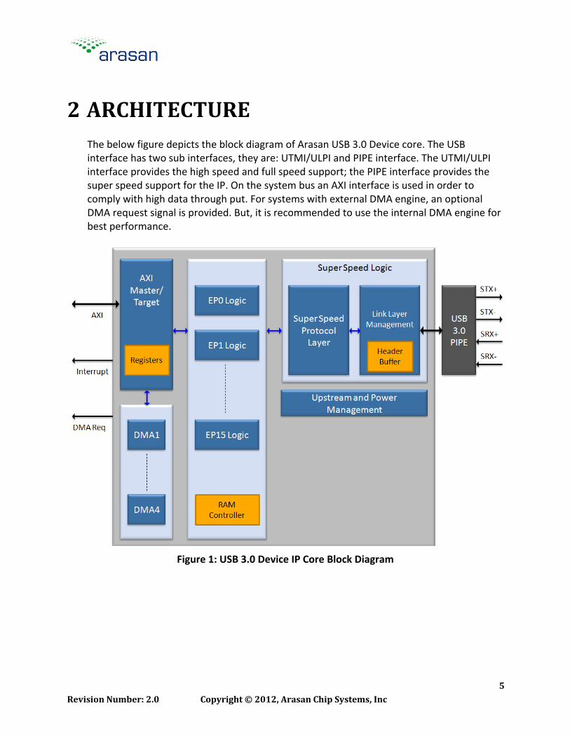
2 ARCHITECTURE
The below figure depicts the block diagram of Arasan USB 3.0 Device core. The USB interface has two sub interfaces, they are: UTMI/ULPI and PIPE interface. The UTMI/ULPI interface provides the high speed and full speed support; the PIPE interface provides the super speed support for the IP. On the system bus an AXI interface is used in order to comply with high data through put. For systems with external DMA engine, an optional DMA request signal is provided. But, it is recommended to use the internal DMA engine for best performance.
Figure 1: USB 3.0 Device IP Core Block Diagram
Revision Number: 2.0 Copyright © 2012, Arasan Chip Systems, Inc
6
2.1 AXI Master/Target Interface The AXI interface for the core provides the system bus interface for the IP. AXI bus interface is preferred over the AHB due to the high bandwidth requirement for the super speed protocol. The table below shows the pin interface for the AXI Master interface. AXI model is responsible for the AXI core connectivity of the IP. There are two sub modules in this block, they are: AXI Master and AXI Slave. The AXI master is responsible for the AXI master specific protocols; and the AXI slave is responsible for AXI slave and endpoint specific protocols. The AXI master is responsible for the following actions: maintaining the device register set through read and write operation from AXI master to the AXI slave interface in the IP. Additionally there is byte enable for write and read specified data. There is a enable signal and acknowledge signal for both read and write operation. The AXI slave is responsible for the following actions: responding the read and write operation from AXI master interface in the IP. Additionally there is byte enable for write and read specified data. There is an enable signal and acknowledge signal for both read and write operation. The AXI interface integrated to the USB2.0 core has a DMA controller. A wrapper that integrates AXI master core with a DMAC controller is the USB device core that has AXI Master along with DMA and AXI Slave. The Driver model at the backend of the device writes the device specific information to the USB device registers by means of AXI interfaces.
2.2 DMA Module There is a ping pong buffer in the front end. The size of ping pong buffer is same as the maximum packet size. The CRC is calculated on the fly while data is being stored on to the ping pong buffer and the buffer flushed out in case of CRC error. We have one FIFO per endpoint that we support. This FIFO can be of programmable size. The DMA descriptor structure can support a maximum of 256 descriptors. If we support 16 endpoints and each endpoint can support up to 16 SID's then the descriptors size will be 256. Each endpoint will have a set of registers in its Descriptor structure registers. There are 2 state machines, one to update the DMA Descriptor structure and the other for data transfer between FIFO and AXI interface. The Link structure consists of the DMA Descriptor list structure for each endpoints/tags. S/W will program the initial values. The Link Update State Machine will update the Descriptor structure when needed. The FIFO Interface is where multiple endpoints data reside. The LUT has a set of addresses where each address corresponds to one endpoint When a request is received/send its tag ID is compared to the set of addresses in the LUT and if there is a hit the DMA State Machine points to that particular set of DMA Descriptor structure. The number of entries in the LUT is programmable which will be equal to the number of endpoints we need to
Revision Number: 2.0 Copyright © 2012, Arasan Chip Systems, Inc
7
support. Each endpoint will have a set of registers in its Descriptor Structure registers. The DMA Descriptor structure is defined in Fig2. The DMA structure may be different for both transmit and receive. If the OWN bit is ‘1’ the descriptor is valid else not ready.
2.3 EP Logic Device has 15 endpoints from ep0 to ep14. There is a default endpoint called control endpoint ep0. 7 endpoints are IN endpoints and the other 7 are OUT endpoints. Control endpoint is responsible for maintaining device state. Control transfers are handled by the control endpoint. IN and OUT endpoints are responsible for receiving and sending data from/to host respectively. Each endpoint has a data buffer to store data within.
2.4 RAM Controller Endpoint RAM operation is controlled by this block. This block generates the read and writes control signals to access and dump the data inside the RAM. The read/ write pointers access is shared by USB side as well as backend side.
2.5 Super Speed Logic Super speed module is responsible for the super speed connectivity of the IP. There are two sub modules in this block, they are: Link Management Layer and Protocol layer. The Link Management Layer is responsible for the link layer specific protocols; and the protocol layer is responsible to handle endpoint specific protocols.
2.5.1 Super Speed Protocol Layer The protocol layer is responsible to maintain the endpoint specific protocol as required by the USB 3.0 specification. The storage for the data packet is stored in the endpoint specific block and not in this block.
2.5.2 Link Management Layer The Link Management Layer is responsible for the following actions: maintaining the link state machine, maintaining header sequence numbers, maintaining header buffers, and maintain handshaking during reception or transmission of header packets. Additionally, this layer injects the SKIP order sets when the link is in U0 state. The key registers maintained in this layer are TX Header sequence, TX ACK Header sequence, Rx Header Sequence, Rx Credit buffer, and Remote Rx Credit buffer. There is a buffer for 4 Header packets for both Transmit and Receive path. Also, a timer is included in this module, which is shared between different LTSSM. This timer works on a very slow derived clock in order to reduce the gate count and to increase the performance. Appendix A shows an example scenario of link initialization and link training in detail.
Revision Number: 2.0 Copyright © 2012, Arasan Chip Systems, Inc
8
2.6 Upstream and Power Management Device maintains 3 low power states at link lever. They are U1, U2 and U3. U1 is a low power state where no packets are to be transmitted and both ports agree to enter a link state where a Super Speed PHY can be placed into a low power state U2 is a link state where more power saving opportunities are allowed compare to U1, but with an increased exit latency U3 is a link state where a device is put into a suspend state. Significant link and device powers are saved. Only upstream host can initiate U3 entry whereas device can only initiate U1 and U2 entry. But device can initiate U3 exit.

Revision Number: 2.0 Copyright © 2012, Arasan Chip Systems, Inc
9
3 SIGNAL INTERFACES
The USB 3.0 Device has the following interface signals
USB 3.0 Pipe Interface
UTMI/ULPI Interface
AXI Interface
AXI Master Interface
AXI Target Interface
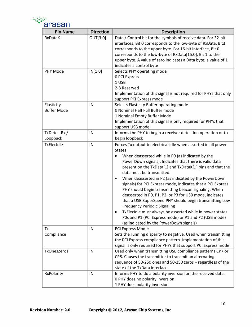
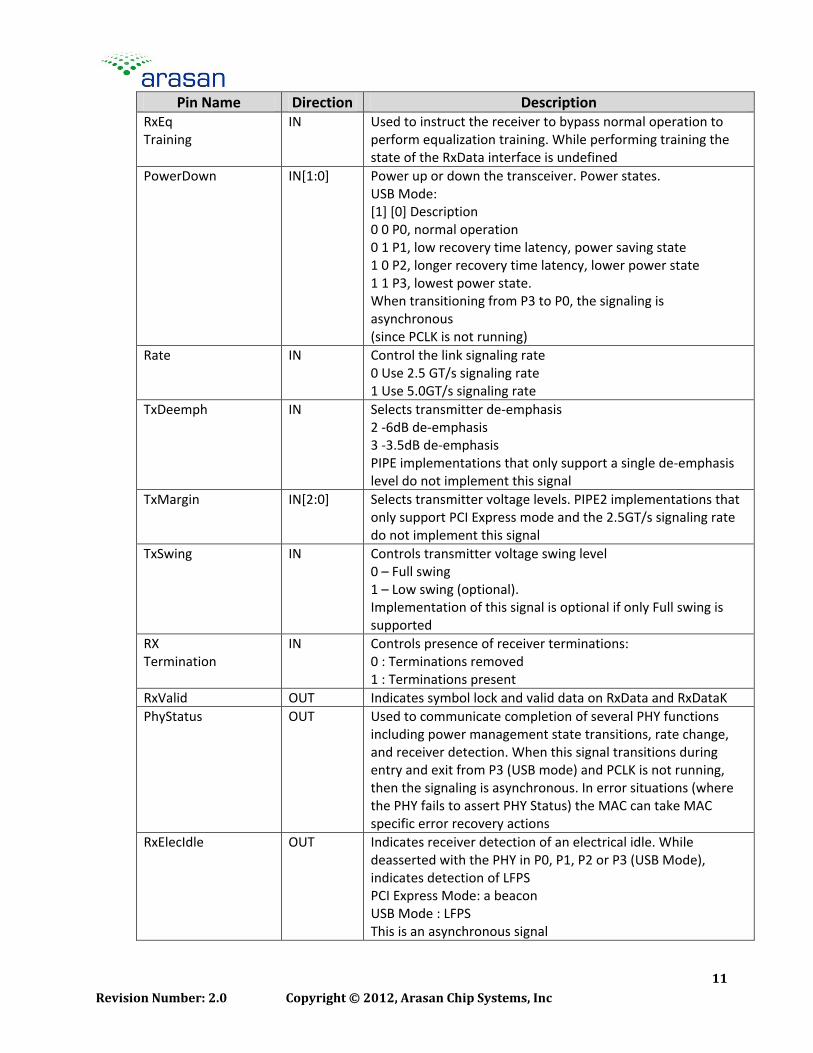
3.1 USB 3.0 PIPE Interface
The super speed support for the core is provided using the PIPE interface. A 16 bit (250 MHz) PIPE interface is used in this IP. This PIPE interface provides the link management unit the super speed connectivity for the IP. The table below depicts the pin interface for the USB 3.0 PIPE interface.
Table 1: USB 3.0 PIPE Pin Interface
Pin Name Direction Description Pclk IN PIPE operating clock and the max freq is 250 MHz
Rst_n OUT Asynchronous reset to the module
Tx+ ,Tx- OUT USB Differential Output from the PHY
TxData
IN[31:0] 32 bit data line for the transmit data, valid only when the txelecidle is not active. Bits [7:0] are the first symbol to be transmitted, and bits [15:8] are the second symbol. For the 32-bit interface, 32 bits represent the 4 symbols of transmit data. Bits [23:16] are the third symbol to be transmitted, and bits [31:24] are the fourth symbol
TxDataK
IN[3:0] Data / Control for the symbols of transmit data. For 32-bit interfaces, Bit 0 corresponds to the low-byte of TxData, Bit3 corresponds to the upper byte. For 16-bit interfaces, Bit 0 corresponds to the low-byte of TxData, Bit 1 to the upper byte. A value of zero indicates a data byte, a value of 1 indicates a control byte
Rx+, Rx- IN USB Differential Input from the PHY
RxData OUT[31:0] Data output bus. For 16-bit interface, 16 bits represents 2 symbols of receive data. Bits [7:0] are the first symbol received, and bits [15:8] are the second symbol. For the 32 bit interface, 32 bits represent the 4 symbols of receive data. Bits [23:16] are the third symbol received, and bits [31:24] are the fourth symbol received
Revision Number: 2.0 Copyright © 2012, Arasan Chip Systems, Inc
10
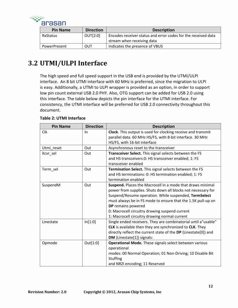
Pin Name Direction Description RxDataK
OUT[3:0] Data / Control bit for the symbols of receive data. For 32-bit interfaces, Bit 0 corresponds to the low-byte of RxData, Bit3 corresponds to the upper byte. For 16-bit interface, Bit 0 corresponds to the low-byte of RxData[15:0], Bit 1 to the upper byte. A value of zero indicates a Data byte; a value of 1 indicates a control byte
PHY Mode
IN[1:0] Selects PHY operating mode 0 PCI Express 1 USB 2-3 Reserved Implementation of this signal is not required for PHYs that only support PCI Express mode
Elasticity Buffer Mode
IN
Selects Elasticity Buffer operating mode 0 Nominal Half Full Buffer mode 1 Nominal Empty Buffer Mode Implementation of this signal is only required for PHYs that support USB mode
TxDetectRx / Loopback
IN Informs the PHY to begin a receiver detection operation or to begin loopback
TxElecIdle
IN Forces Tx output to electrical idle when asserted in all power States
When deasserted while in P0 (as indicated by the PowerDown signals), Indicates that there is valid data present on the TxData[..] and TxDataK[..] pins and that the data must be transmitted.
When deasserted in P2 (as indicated by the PowerDown signals) for PCI Express mode, indicates that a PCI Express PHY should begin transmitting beacon signaling. When deasserted in P0, P1, P2, or P3 for USB mode, indicates that a USB SuperSpeed PHY should begin transmitting Low Frequency Periodic Signaling
TxElecIdle must always be asserted while in power states P0s and P1 (PCI Express mode) or P1 and P2 (USB mode) (as indicated by the PowerDown signals)
Tx Compliance
IN
PCI Express Mode: Sets the running disparity to negative. Used when transmitting the PCI Express compliance pattern. Implementation of this signal is only required for PHYs that support PCI Express mode
TxOnesZeros
IN Used only when transmitting USB compliance patterns CP7 or CP8. Causes the transmitter to transmit an alternating sequence of 50-250 ones and 50-250 zeros – regardless of the state of the TxData interface
RxPolarity
IN Informs PHY to do a polarity inversion on the received data. 0 PHY does no polarity inversion 1 PHY does polarity inversion
Revision Number: 2.0 Copyright © 2012, Arasan Chip Systems, Inc
11
Pin Name Direction Description RxEq Training
IN
Used to instruct the receiver to bypass normal operation to perform equalization training. While performing training the state of the RxData interface is undefined
PowerDown
IN[1:0] Power up or down the transceiver. Power states. USB Mode: [1] [0] Description 0 0 P0, normal operation 0 1 P1, low recovery time latency, power saving state 1 0 P2, longer recovery time latency, lower power state 1 1 P3, lowest power state. When transitioning from P3 to P0, the signaling is asynchronous (since PCLK is not running)
Rate
IN Control the link signaling rate 0 Use 2.5 GT/s signaling rate 1 Use 5.0GT/s signaling rate
TxDeemph
IN Selects transmitter de-emphasis 2 -6dB de-emphasis 3 -3.5dB de-emphasis PIPE implementations that only support a single de-emphasis level do not implement this signal
TxMargin
IN[2:0] Selects transmitter voltage levels. PIPE2 implementations that only support PCI Express mode and the 2.5GT/s signaling rate do not implement this signal
TxSwing
IN Controls transmitter voltage swing level 0 – Full swing 1 – Low swing (optional). Implementation of this signal is optional if only Full swing is supported
RX Termination
IN
Controls presence of receiver terminations: 0 : Terminations removed 1 : Terminations present
RxValid OUT Indicates symbol lock and valid data on RxData and RxDataK
PhyStatus
OUT Used to communicate completion of several PHY functions including power management state transitions, rate change, and receiver detection. When this signal transitions during entry and exit from P3 (USB mode) and PCLK is not running, then the signaling is asynchronous. In error situations (where the PHY fails to assert PHY Status) the MAC can take MAC specific error recovery actions
RxElecIdle
OUT Indicates receiver detection of an electrical idle. While deasserted with the PHY in P0, P1, P2 or P3 (USB Mode), indicates detection of LFPS PCI Express Mode: a beacon USB Mode : LFPS This is an asynchronous signal
Revision Number: 2.0 Copyright © 2012, Arasan Chip Systems, Inc
12
Pin Name Direction Description RxStatus
OUT[2:0] Encodes receiver status and error codes for the received data stream when receiving data
PowerPresent OUT Indicates the presence of VBUS
3.2 UTMI/ULPI Interface
The high speed and full speed support in the USB end is provided by the UTMI/ULPI interface. An 8 bit UTMI interface with 60 MHz is preferred, since the migration to ULPI is easy. Additionally, a UTMI to ULPI wrapper is provided as an option, in order to support low pin count external USB 2.0 PHY. Also, OTG support can be added for USB 2.0 using this interface. The table below depicts the pin interface for the UTMI interface. For consistency, the UTMI interface will be preferred for USB 2.0 connectivity throughout this document.
Table 2: UTMI Interface
Pin Name Direction Description Clk
In Clock. This output is used for clocking receive and transmit parallel data. 60 MHz HS/FS, with 8-bit interface. 30 MHz HS/FS, with 16-bit interface
Utmi_reset Out Asynchronous reset to the transceiver
Xcvr_sel
Out Transceiver Select. This signal selects between the FS and HS transceivers:0: HS transceiver enabled; 1: FS transceiver enabled
Term_sel
Out Termination Select. This signal selects between the FS and HS terminations: 0: HS termination enabled; 1: FS termination enabled
SuspendM
Out Suspend. Places the Macrocell in a mode that draws minimal power from supplies. Shuts down all blocks not necessary for Suspend/Resume operation. While suspended, TermSelect must always be in FS mode to ensure that the 1.5K pull-up on DP remains powered 0: Macrocell circuitry drawing suspend current 1: Macrocell circuitry drawing normal current
Linestate
In[1:0] Single ended receivers. They are combinatorial until a"usable" CLK is available then they are synchronized to CLK. They directly reflect the current state of the DP (Linestate[0]) and DM (Linestate[1]) signals:
Opmode
Out[1:0] Operational Mode. These signals select between various operational modes: 00 Normal Operation; 01 Non-Driving; 10 Disable Bit Stuffing and NRZI encoding; 11 Reserved

Revision Number: 2.0 Copyright © 2012, Arasan Chip Systems, Inc
13
Pin Name Direction Description Datatx
Out[7:0] DataTx. 8-bit parallel USB data input bus. When DataBus16_8 = 1 this bus transfers the low byte of 16-bit transmit data. When DataBus16_8 = 0 all transmit data is transferred over this bus
Txvalid
Out Transmit Valid. Indicates that the DataIn bus is valid. The assertion of Transmit Valid initiates SYNC on the USB. The negation of Transmit Valid initates EOP on the USB. In HS (XcvrSelect = 0) mode, the SYNC pattern must be asserted on the USB between 8 and 16 bit times after the assertion of TXValid is detected by the Transmit State Machine. See section 6.4 for more information
Txready
In Transmit Data Ready. If TXValid is asserted, the SIE must always have data available for clocking in to the TX Holding Register on the rising edge of CLK. If TXValid is TRUE and TXReady is asserted at the rising edge of CLK, the UTM will load the data on the Datatx bus into the TX Holding Register on the next rising edge of CLK, at that time, SIE should immediately present the data for next transfer on the DataIn bus. If TXValid is asserted and TXReady is negated, the SIE must hold the previously asserted data on the Datatx bus. From the time TXValid is negated, TXReady is a don't care for the SIE.
Datarx
In[7:0] Datarx. 8-bit parallel USB data output bus. When DataBus16_8 = 1 this bus transfers the low byte of 16-bit receive data. When DataBus16_8 = 0 all receive data is transferred over this bus
Rxvalid
In Receive Data Valid. Indicates that the DataOut bus has valid data. The Receive Data Holding Register is full and ready to be unloaded. The SIE is expected to latch the Datarx bus on the clock edge
Rxvalidh
In Receive Data Valid High. When DataBus16_8 = 1 this signals indicates that the Datarx(8-15) bus is presenting valid receive data. This signal is ignored when DataBus16_8 = 0. This signal is not provided in 8-Bit transceiver implementations.
Rxactive
In Receive Active. Indicates that the receiver state machine has detected SYNC and is active. RXActive is negated after a Bit Stuff Error or an EOP is detected.
Rxerror
In Receive Error.0 Indicates no error. 1 Indicates that a receive error has been detected.
Revision Number: 2.0 Copyright © 2012, Arasan Chip Systems, Inc
14
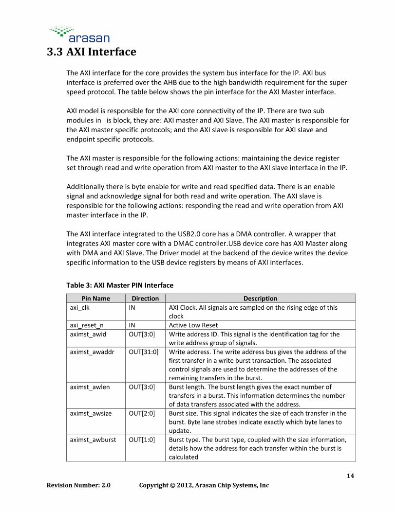
3.3 AXI Interface
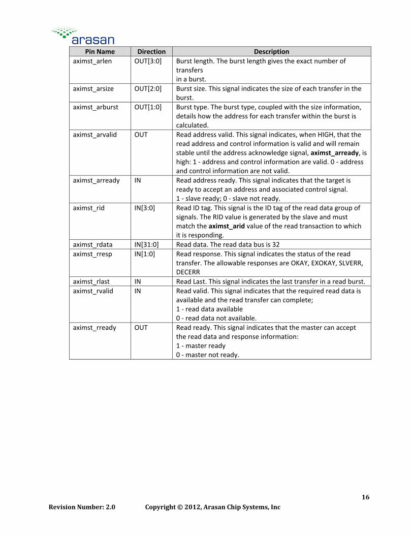
The AXI interface for the core provides the system bus interface for the IP. AXI bus interface is preferred over the AHB due to the high bandwidth requirement for the super speed protocol. The table below shows the pin interface for the AXI Master interface. AXI model is responsible for the AXI core connectivity of the IP. There are two sub modules in is block, they are: AXI master and AXI Slave. The AXI master is responsible for the AXI master specific protocols; and the AXI slave is responsible for AXI slave and endpoint specific protocols. The AXI master is responsible for the following actions: maintaining the device register set through read and write operation from AXI master to the AXI slave interface in the IP. Additionally there is byte enable for write and read specified data. There is an enable signal and acknowledge signal for both read and write operation. The AXI slave is responsible for the following actions: responding the read and write operation from AXI master interface in the IP. The AXI interface integrated to the USB2.0 core has a DMA controller. A wrapper that integrates AXI master core with a DMAC controller.USB device core has AXI Master along with DMA and AXI Slave. The Driver model at the backend of the device writes the device specific information to the USB device registers by means of AXI interfaces.
Table 3: AXI Master PIN Interface
Pin Name Direction Description
axi_clk
IN AXI Clock. All signals are sampled on the rising edge of this clock
axi_reset_n IN Active Low Reset
aximst_awid
OUT[3:0] Write address ID. This signal is the identification tag for the write address group of signals.
aximst_awaddr
OUT[31:0] Write address. The write address bus gives the address of the first transfer in a write burst transaction. The associated control signals are used to determine the addresses of the remaining transfers in the burst.
aximst_awlen
OUT[3:0] Burst length. The burst length gives the exact number of transfers in a burst. This information determines the number of data transfers associated with the address.
aximst_awsize
OUT[2:0] Burst size. This signal indicates the size of each transfer in the burst. Byte lane strobes indicate exactly which byte lanes to update.
aximst_awburst
OUT[1:0]
Burst type. The burst type, coupled with the size information, details how the address for each transfer within the burst is calculated
Revision Number: 2.0 Copyright © 2012, Arasan Chip Systems, Inc
15
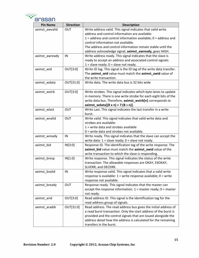
Pin Name Direction Description
aximst_awvalid
OUT Write address valid. This signal indicates that valid write address and control information are available: 1 = address and control information available; 0 = address and control information not available. The address and control information remain stable until the address acknowledge signal, aximst_awready, goes HIGH.
aximst_awready
IN
Write address ready. This signal indicates that the slave is ready to accept an address and associated control signals: 1 = slave ready; 0 = slave not ready.
aximst_wid
OUT[3:0] Write ID tag. This signal is the ID tag of the write data transfer. The aximst_wid value must match the aximst_awid value of the write transaction.
aximst_wdata OUT[31:0] Write data. The write data bus is 32 bits wide
aximst_wstrb
OUT[3:0] Write strobes. This signal indicates which byte lanes to update in memory. There is one write strobe for each eight bits of the write data bus. Therefore, aximst_wstrb[n] corresponds to aximst_wdata[(8 x n) + 7:(8 x n)].
aximst_wlast OUT Write Last. This signal indicates the last transfer in a write burst.
aximst_wvalid
OUT Write valid. This signal indicates that valid write data and strobes are available: 1 = write data and strobes available 0 = write data and strobes not available.
aximst_wready
IN Write ready. This signal indicates that the slave can accept the write data: 1 = slave ready; 0 = slave not ready.
aximst_bid
IN[3:0] Response ID. The identification tag of the write response. The aximst_bid value must match the aximst_awid value of the write transaction to which the slave is responding.
aximst_bresp
IN[1:0] Write response. This signal indicates the status of the write transaction. The allowable responses are OKAY, EXOKAY, SLVERR, and DECERR.
aximst_bvalid
IN Write response valid. This signal indicates that a valid write response is available: 1 = write response available; 0 = write response not available.
aximst_bready
OUT Response ready. This signal indicates that the master can accept the response information. 1 = master ready; 0 = master not ready.
aximst_arid
OUT[3:0] Read address ID. This signal is the identification tag for the read address group of signals.
aximst_araddr
OUT[31:0] Read address. The read address bus gives the initial address of a read burst transaction. Only the start address of the burst is provided and the control signals that are issued alongside the address detail how the address is calculated for the remaining transfers in the burst.
Revision Number: 2.0 Copyright © 2012, Arasan Chip Systems, Inc
16
Pin Name Direction Description
aximst_arlen
OUT[3:0] Burst length. The burst length gives the exact number of transfers in a burst.
aximst_arsize
OUT[2:0] Burst size. This signal indicates the size of each transfer in the burst.
aximst_arburst
OUT[1:0] Burst type. The burst type, coupled with the size information, details how the address for each transfer within the burst is calculated.
aximst_arvalid
OUT Read address valid. This signal indicates, when HIGH, that the read address and control information is valid and will remain stable until the address acknowledge signal, aximst_arready, is high: 1 - address and control information are valid. 0 - address and control information are not valid.
aximst_arready
IN Read address ready. This signal indicates that the target is ready to accept an address and associated control signal. 1 - slave ready; 0 - slave not ready.
aximst_rid
IN[3:0] Read ID tag. This signal is the ID tag of the read data group of signals. The RID value is generated by the slave and must match the aximst_arid value of the read transaction to which it is responding.
aximst_rdata IN[31:0] Read data. The read data bus is 32
aximst_rresp
IN[1:0] Read response. This signal indicates the status of the read transfer. The allowable responses are OKAY, EXOKAY, SLVERR, DECERR
aximst_rlast IN Read Last. This signal indicates the last transfer in a read burst.
aximst_rvalid
IN Read valid. This signal indicates that the required read data is available and the read transfer can complete; 1 - read data available 0 - read data not available.
aximst_rready
OUT Read ready. This signal indicates that the master can accept the read data and response information: 1 - master ready 0 - master not ready.
Revision Number: 2.0 Copyright © 2012, Arasan Chip Systems, Inc
17
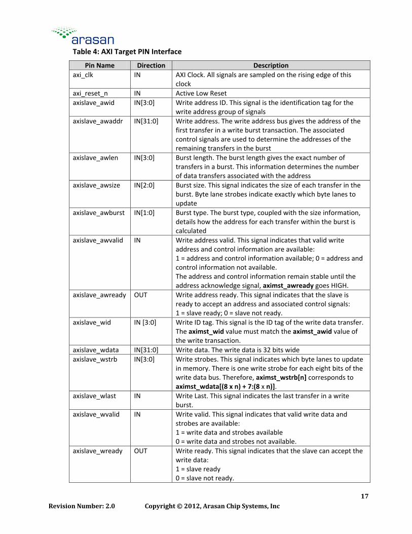
Table 4: AXI Target PIN Interface
Pin Name Direction Description
axi_clk
IN AXI Clock. All signals are sampled on the rising edge of this clock
axi_reset_n IN Active Low Reset
axislave_awid
IN[3:0] Write address ID. This signal is the identification tag for the write address group of signals
axislave_awaddr
IN[31:0] Write address. The write address bus gives the address of the first transfer in a write burst transaction. The associated control signals are used to determine the addresses of the remaining transfers in the burst
axislave_awlen
IN[3:0] Burst length. The burst length gives the exact number of transfers in a burst. This information determines the number of data transfers associated with the address
axislave_awsize
IN[2:0] Burst size. This signal indicates the size of each transfer in the burst. Byte lane strobes indicate exactly which byte lanes to update
axislave_awburst
IN[1:0] Burst type. The burst type, coupled with the size information, details how the address for each transfer within the burst is calculated
axislave_awvalid
IN Write address valid. This signal indicates that valid write address and control information are available: 1 = address and control information available; 0 = address and control information not available. The address and control information remain stable until the address acknowledge signal, aximst_awready goes HIGH.
axislave_awready
OUT Write address ready. This signal indicates that the slave is ready to accept an address and associated control signals: 1 = slave ready; 0 = slave not ready.
axislave_wid
IN [3:0] Write ID tag. This signal is the ID tag of the write data transfer. The aximst_wid value must match the aximst_awid value of the write transaction.
axislave_wdata IN[31:0] Write data. The write data is 32 bits wide
axislave_wstrb
IN[3:0] Write strobes. This signal indicates which byte lanes to update in memory. There is one write strobe for each eight bits of the write data bus. Therefore, aximst_wstrb[n] corresponds to aximst_wdata[(8 x n) + 7:(8 x n)].
axislave_wlast IN Write Last. This signal indicates the last transfer in a write burst.
axislave_wvalid
IN Write valid. This signal indicates that valid write data and strobes are available: 1 = write data and strobes available 0 = write data and strobes not available.
axislave_wready
OUT Write ready. This signal indicates that the slave can accept the write data: 1 = slave ready 0 = slave not ready.
Revision Number: 2.0 Copyright © 2012, Arasan Chip Systems, Inc
18
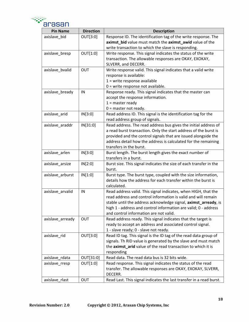
Pin Name Direction Description
axislave_bid
OUT[3:0] Response ID. The identification tag of the write response. The aximst_bid value must match the aximst_awid value of the write transaction to which the slave is responding.
axislave_bresp
OUT[1:0] Write response. This signal indicates the status of the write transaction. The allowable responses are OKAY, EXOKAY, SLVERR, and DECERR.
axislave_bvalid
OUT Write response valid. This signal indicates that a valid write response is available: 1 = write response available 0 = write response not available.
axislave_bready
IN Response ready. This signal indicates that the master can accept the response information. 1 = master ready 0 = master not ready.
axislave_arid
IN[3:0] Read address ID. This signal is the identification tag for the read address group of signals.
axislave_araddr
IN[31:0] Read address. The read address bus gives the initial address of a read burst transaction. Only the start address of the burst is provided and the control signals that are issued alongside the address detail how the address is calculated for the remaining transfers in the burst.
axislave_arlen
IN[3:0] Burst length. The burst length gives the exact number of transfers in a burst.
axislave_arsize
IN[2:0] Burst size. This signal indicates the size of each transfer in the burst.
axislave_arburst
IN[1:0] Burst type. The burst type, coupled with the size information, details how the address for each transfer within the burst is calculated.
axislave_arvalid
IN Read address valid. This signal indicates, when HIGH, that the read address and control information is valid and will remain stable until the address acknowledge signal, aximst_arready, is high 1 - address and control information are valid; 0 - address and control information are not valid.
axislave_arready
OUT Read address ready. This signal indicates that the target is ready to accept an address and associated control signal. 1 - slave ready; 0 - slave not ready.
axislave_rid
OUT[3:0] Read ID tag. This signal is the ID tag of the read data group of signals. Th RID value is generated by the slave and must match the aximst_arid value of the read transaction to which it is responding
axislave_rdata OUT[31:0] Read data. The read data bus is 32 bits wide.
axislave_rresp
OUT[1:0] Read response. This signal indicates the status of the read transfer. The allowable responses are OKAY, EXOKAY, SLVERR, DECERR.
axislave_rlast OUT Read Last. This signal indicates the last transfer in a read burst.
Revision Number: 2.0 Copyright © 2012, Arasan Chip Systems, Inc
19
Pin Name Direction Description
axislave_rvalid
OUT Read valid. This signal indicates that the required read data is available and the read transfer can complete; 1 - read data available; 0 - read data not available.
axislave_rready
IN Read ready. This signal indicates that the master can accept the read data and response information: 1 - master ready; 0 - master not ready.
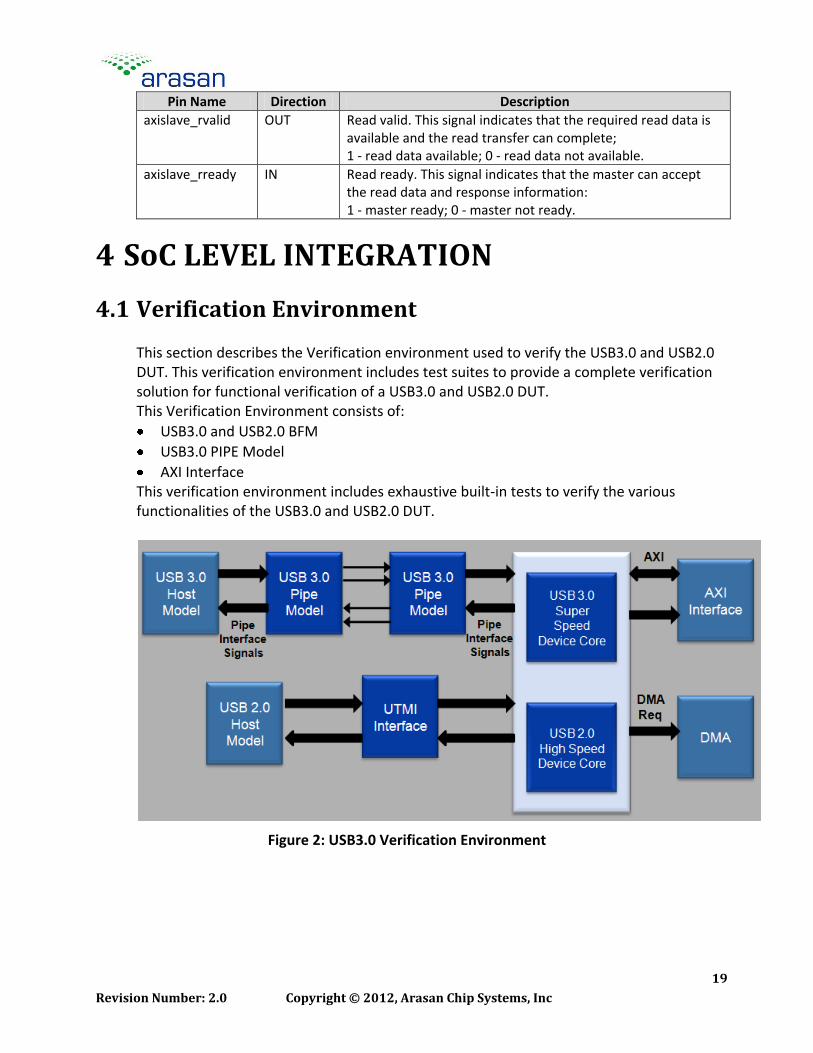
4 SoC LEVEL INTEGRATION
4.1 Verification Environment
This section describes the Verification environment used to verify the USB3.0 and USB2.0 DUT. This verification environment includes test suites to provide a complete verification solution for functional verification of a USB3.0 and USB2.0 DUT. This Verification Environment consists of:
USB3.0 and USB2.0 BFM
USB3.0 PIPE Model
AXI Interface This verification environment includes exhaustive built-in tests to verify the various functionalities of the USB3.0 and USB2.0 DUT.
Figure 2: USB3.0 Verification Environment
Revision Number: 2.0 Copyright © 2012, Arasan Chip Systems, Inc
20
4.2 IP Deliverables
The IP package consists of the following:
RMM Compliant Synthesizable RTL design in Verilog
Easy-to-use test environment
Synthesis scripts
Technical documents
5 RELATED PRODUCTS
USB 3.0 Device Stack