datasheet shf d837a v002 · PDF file4 Calculation based on typical results of setup without...
12
SHF reserves the right to change specifications and design without notice – SHF D837 A - V002 – May 26, 2017 Page 1/12 SHF Communication Technologies AG Wilhelm-von-Siemens-Str. 23D • 12277 Berlin • Germany Phone ++49 30 772 051-0 • Fax ++49 30 753 10 78 E-Mail: [email protected] • Web: http://www.shf.de Datasheet SHF D837 A Differential to Single-Ended Linear Broadband Amplifier
Transcript of datasheet shf d837a v002 · PDF file4 Calculation based on typical results of setup without...

SHF reserves the right to change specifications and design without notice – SHF D837 A - V002 – May 26, 2017 Page 1/12
SHF Communication Technologies AG
Wilhelm-von-Siemens-Str. 23D • 12277 Berlin • Germ any
Phone ++49 30 772 051-0 • Fax ++49 30 753 10 78
E-Mail: [email protected] • Web: http://www.shf.de
Datasheet SHF D837 A
Differential to Single-Ended Linear Broadband Amplifier
SHF reserves the right to change specifications and design without notice – SHF D837 A - V002 – May 26, 2017 Page 2/12
Description
The SHF D837 A is a differential input, single-ended output linear amplifier designed for PAM4 and 16QAM applications. The single-ended output drive amplitude of up to at least 3 V linear is particularly well suited for state-of-the-art single-drive DP-16QAM modulators. When driven from the differential outputs of a high performance DAC, the common-mode rejection characteristic of this differential input design helps to maintain the linearity and resolution of the DAC.
This amplifier is of a single chip design based on state-of-the-art commercial GaAs process, housed in a special low loss carrier PCB environment to maintain wide bandwidth and low group delay variation, necessary for high performance operation.
Like other amplifiers in the product family, this amplifier enjoys the same benefit of an internal voltage regulation to protect against accidental reverse voltage connection. Similarly, the output amplitude and crossing adjustment using software control via an USB connection. Once adjusted, the connection can be removed until the next time.
Ease of Use
Upon delivery, the amplifier is already pre-set to deliver maximum gain, maximum output amplitude and nominally 50% crossing.
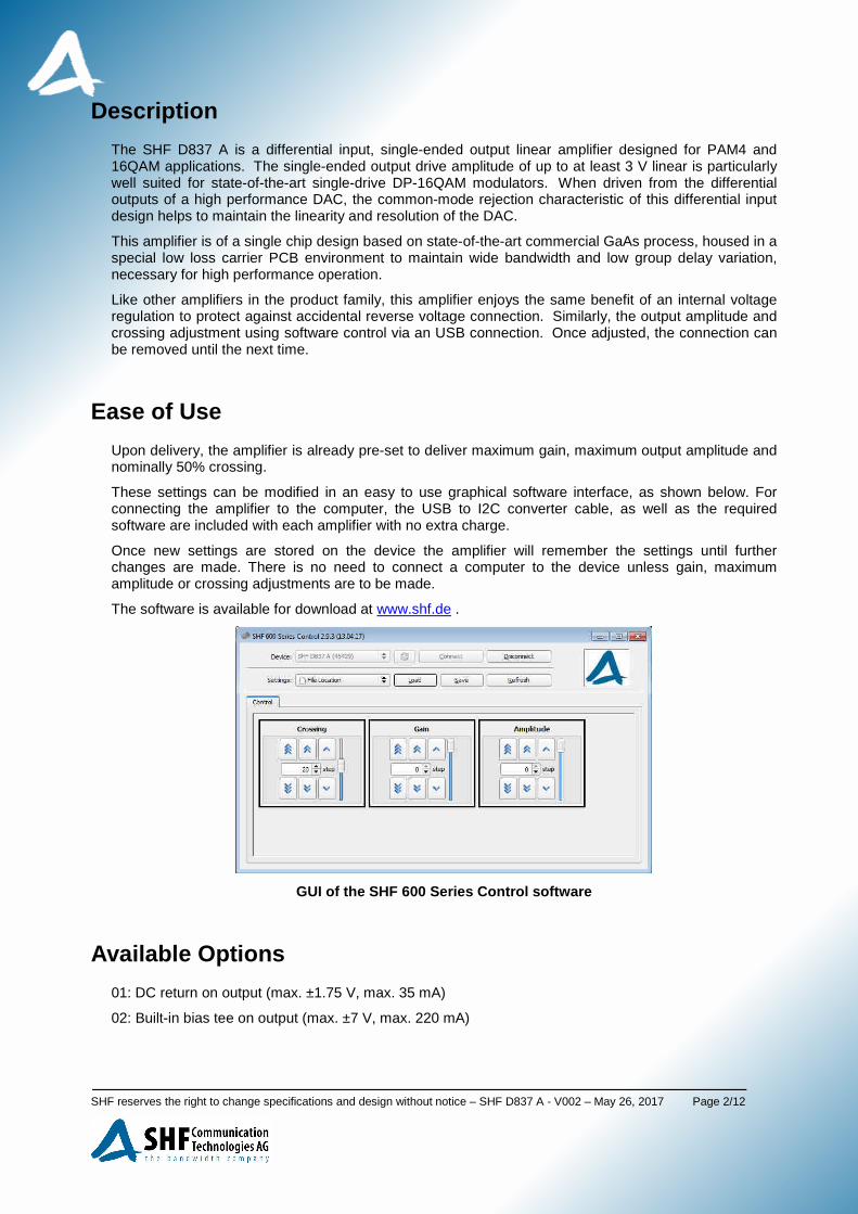
These settings can be modified in an easy to use graphical software interface, as shown below. For connecting the amplifier to the computer, the USB to I2C converter cable, as well as the required software are included with each amplifier with no extra charge.
Once new settings are stored on the device the amplifier will remember the settings until further changes are made. There is no need to connect a computer to the device unless gain, maximum amplitude or crossing adjustments are to be made.
The software is available for download at www.shf.de .
GUI of the SHF 600 Series Control software
Available Options
01: DC return on output (max. ±1.75 V, max. 35 mA)
02: Built-in bias tee on output (max. ±7 V, max. 220 mA)

SHF reserves the right to change specifications and design without notice – SHF D837 A - V002 – May 26, 2017 Page 3/12
Specifications – SHF D837
Parameter Unit Symbol Min Typ Max Conditions
Absolute Maximum Ratings
Maximum RF Input Power in Operation
dBm
V Pin max
4
1
peak to peak voltage
Maximum RF Input Power without Power Supply
dBm
V Pin max
10
2
peak to peak voltage
DC Voltage at RF Input V ±9 AC coupled input
DC Voltage at RF Output V ±7 AC coupled output
Supply Voltage V 8 12 0.4 A, reverse voltage protected
Case Temperature1 Tcase °C 10 40 50
Electrical Characteristics (At 40°C case temperature, unless otherwise specified)
High Frequency 3 dB Point
GHz fHIGH InP 45 single ended2, non-inverting input
GHz fHIGH InN 32 single ended2, inverting input
GHz fHIGH Diff 35 Calculated from single ended
Low Frequency 3 dB Point kHz fLOW 50 each inputs
Gain dB S21 9 10 measured at Pin= -27 dBm
Gain Ripple dB ∆S21 ±0.5 ±1 40 MHz…25 GHz, relative to gain-slope
Max. Gain Reduction dB -2.5 -3 -4 Control via software interface
Output Power at 1 dB Compression
dBm
V P01dB
12
2.5
13
2.8
10 MHz…25 GHz
peak to peak voltage
Output Power at 2 dB Compression
dBm
V P02dB
15
3.6
16
4.0
10 MHz…25 GHz
peak to peak voltage
Output Power at 3 dB Compression
dBm
V P03dB
16
4.0
17
4.5
10 MHz…25 GHz
peak to peak voltage
3rd Order Intercept Point dBm IP3 25
Max. RF Input for Linear Operation
dBm
V Pin lin
-3
0.45
I.e. Pout ≤ P01dB
peak to peak voltage, single ended
Max. Output Power Reduction
dB tbd
Pin ≥ - 2 dBm
Crossing might need to be readjusted by using the crossing control feature.
Control via software interface
Crossing Control Range
% -4 4 Control via software interface
Vout ~2.5 V
1 If operated with heat sink (part of the delivery) at room temperature there is no need for additional cooling. 2 Single ended measurement condition with -27dBm input power

SHF reserves the right to change specifications and design without notice – SHF D837 A - V002 – May 26, 2017 Page 4/12
Parameter Unit Symbol Min Typ Max Conditions
Input Reflection dB S11 -15
-12
-10
< 10 GHz, single ended
< 30 GHz, single ended
Output Reflection dB S22 -10 -9 < 30 GHz
Rise Time/Fall Time ps tr/tf
7
11
20%...80%, 2.5 V ≤ Vout ≤ 3.5 V
Deconvoluted 3, 4
Full Setup 3
Jitter fs JRMS
500
580
550
650
2.5 V ≤ Vout ≤ 3.5 V
Deconvoluted 3, 4
Full Setup 3
Group Delay Ripple ps ±50 40 MHz…30 GHz, 100 MHz aperture
Power Consumption W 2.7 9 V supply voltage
Mechanical Characteristics
Input Connectors 1.85 mm (V) female5
Output Connector 1.85 mm (V) male5
2 Single ended measurement condition with -27dBm input power 3 Measured with: SHF 613 A DAC -> DUT (SHF D837 A) -> Agilent 86100C with 70 GHz sampling head & precision time base. 4 Calculation based on typical results of setup without DUT :
��/������� ��� = �(��/��� ����� �)� − (��/����� ��/���)� = �(��/��� ����� �)� − 11��� �� !����� ��� = "(�� !� ����� �)� − #�� !��� ��/���$� = �(�� !� ����� �)� − 360(�� 5 Other gender configurations are available on request. Other connector types are also available but may impact bandwidth & reflection.
SHF reserves the right to change specifications and design without notice – SHF D837 A - V002 – May 26, 2017 Page 5/12
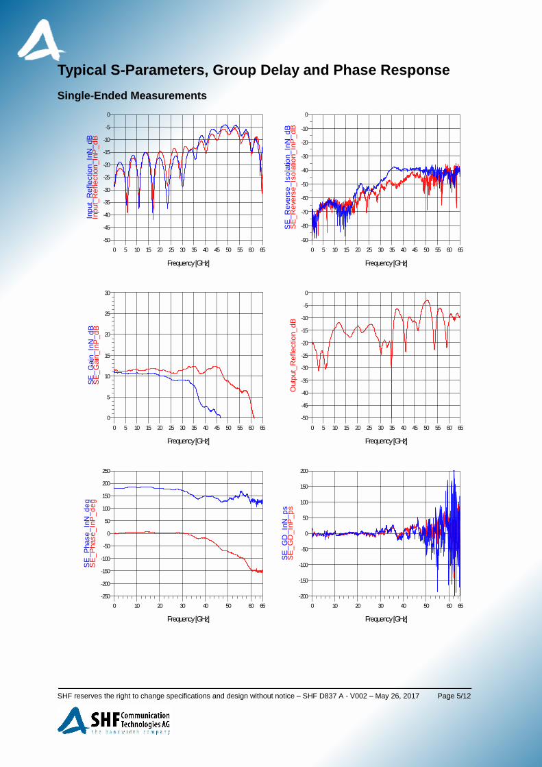
Typical S-Parameters, Group Delay and Phase Respons e
Single-Ended Measurements
5 10 15 20 25 30 35 40 45 50 55 600 65
-45
-40
-35
-30
-25
-20
-15
-10
-5
-50
0
Frequency [GHz]
Inpu
t_R
efle
ctio
n_In
P_d
BIn
put
_R
efle
ctio
n_In
N_
dB
10 20 30 40 50 600 65
-200
-150
-100
-50
0
50
100
150
200
-250
250
Frequency [GHz]
SE
_P
hase
_InP
_de
gS
E_
Pha
se_I
nN_
deg
10 20 30 40 50 600 65
-150
-100
-50
0
50
100
150
-200
200
Frequency [GHz]
SE
_G
D_I
nP_p
sS
E_
GD
_InN
_ps
5 10 15 20 25 30 35 40 45 50 55 600 65
-45
-40
-35
-30
-25
-20
-15
-10
-5
-50
0
Frequency [GHz]
Out
put_
Re
flect
ion_
dB
5 10 15 20 25 30 35 40 45 50 55 600 65
5
10
15
20
25
0
30
Frequency [GHz]
SE
_G
ain_
InP
_dB
SE
_Gai
n_In
N_d
B
5 10 15 20 25 30 35 40 45 50 55 600 65
-80
-70
-60
-50
-40
-30
-20
-10
-90
0
Frequency [GHz]
SE
_R
eve
rse
_Iso
latio
n_In
P_
dBS
E_
Rev
ers
e_I
sola
tion_
InN
_dB
SHF reserves the right to change specifications and design without notice – SHF D837 A - V002 – May 26, 2017 Page 6/12
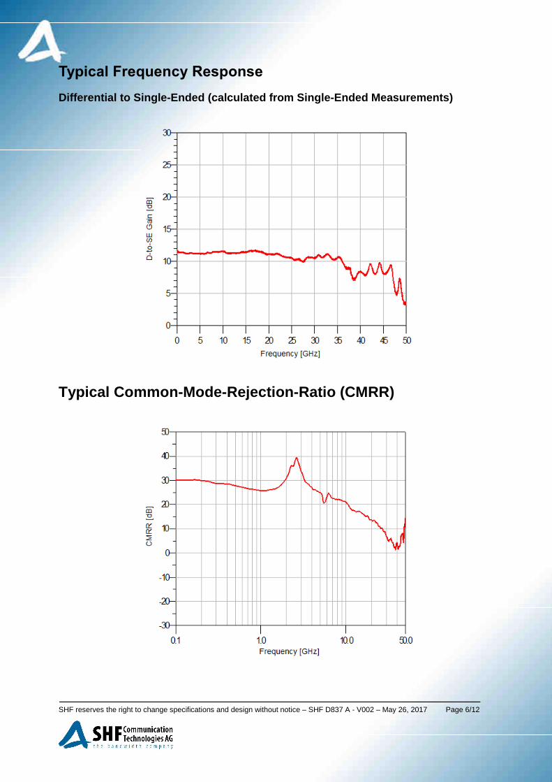
Typical Frequency Response
Differential to Single-Ended (calculated from Singl e-Ended Measurements)
Typical Common-Mode-Rejection-Ratio (CMRR)
SHF reserves the right to change specifications and design without notice – SHF D837 A - V002 – May 26, 2017 Page 7/12
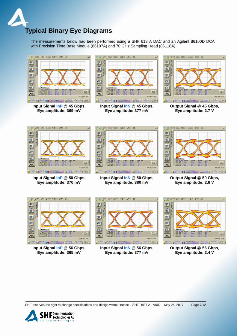
Typical Binary Eye Diagrams
The measurements below had been performed using a SHF 613 A DAC and an Agilent 86100D DCA with Precision Time Base Module (86107A) and 70 GHz Sampling Head (86118A).
Input Signal InP @ 45 Gbps,
Eye amplitude: 369 mV Input Signal InN @ 45 Gbps,
Eye amplitude: 377 mV Output Signal @ 45 Gbps,
Eye amplitude: 2.7 V
Input Signal InP @ 50 Gbps,
Eye amplitude: 370 mV Input Signal InN @ 50 Gbps,
Eye amplitude: 380 mV Output Signal @ 50 Gbps,
Eye amplitude: 2.6 V
Input Signal InP @ 56 Gbps,
Eye amplitude: 365 mV Input Signal InN @ 56 Gbps,
Eye amplitude: 377 mV Output Signal @ 56 Gbps,
Eye amplitude: 2.4 V

SHF reserves the right to change specifications and design without notice – SHF D837 A - V002 – May 26, 2017 Page 8/12
Typical 4-Level Eye diagrams
The measurements below had been performed using a SHF 613 A DAC and an Agilent 86100D DCA with Precision Time Base Module (86107A) and 70 GHz Sampling Head (86118A).
Input Signal InP @ 45 GBaud,
Eye amplitude: 448 mV Input Signal InN @ 45 GBaud,
Eye amplitude: 448 mV Output Signal @ 45 GBaud,
Eye amplitude: 3.1 V
Input Signal InP @ 50 GBaud,
Eye amplitude: 442 mV Input Signal InN @ 50 GBaud,
Eye amplitude: 450 mV Output Signal @ 50 GBaud,
Eye amplitude: 3.1 V
Input Signal InP @ 56 GBaud,
Eye amplitude: 450 mV Input Signal InN @ 56 GBaud,
Eye amplitude: 450 mV Output Signal @ 56 GBaud,
Eye amplitude: 3.0 V
SHF reserves the right to change specifications and design without notice – SHF D837 A - V002 – May 26, 2017 Page 9/12
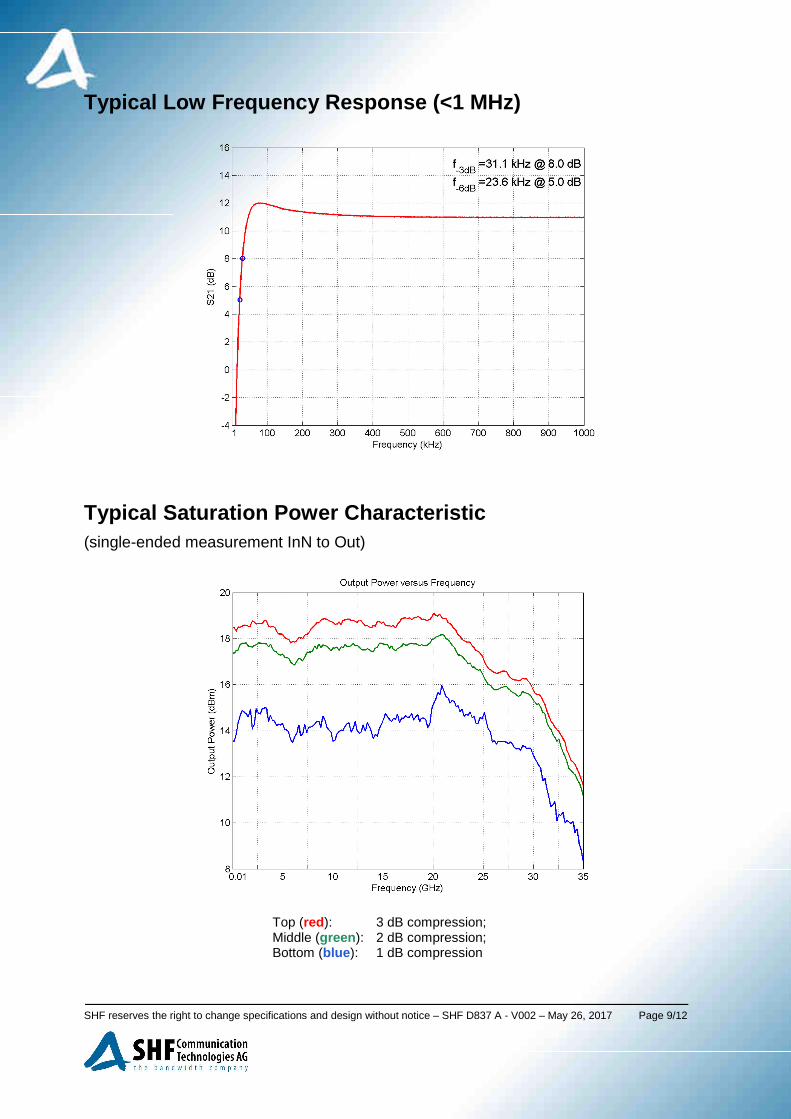
Typical Low Frequency Response (<1 MHz)
Typical Saturation Power Characteristic (single-ended measurement InN to Out)
Top (red ): 3 dB compression; Middle (green ): 2 dB compression; Bottom (blue ): 1 dB compression
SHF reserves the right to change specifications and design without notice – SHF D837 A - V002 – May 26, 2017 Page 10/12
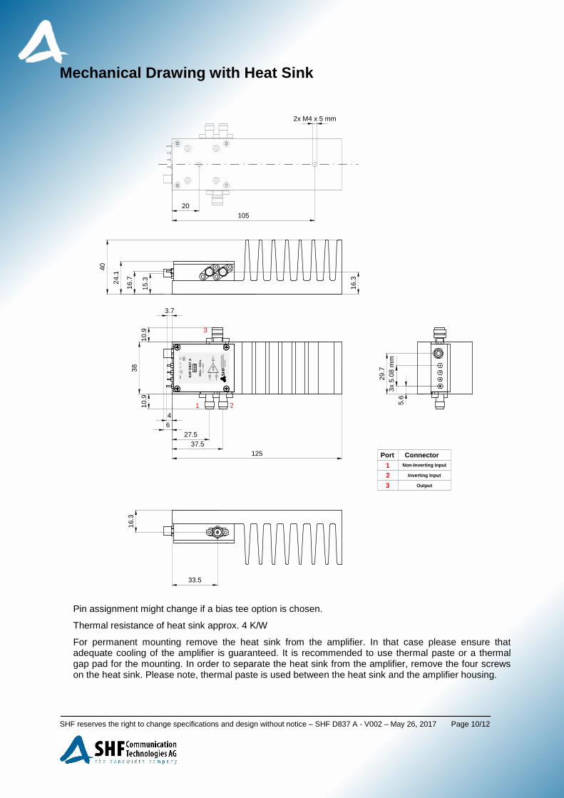
Mechanical Drawing with Heat Sink
Pin assignment might change if a bias tee option is chosen.
Thermal resistance of heat sink approx. 4 K/W
For permanent mounting remove the heat sink from the amplifier. In that case please ensure that adequate cooling of the amplifier is guaranteed. It is recommended to use thermal paste or a thermal gap pad for the mounting. In order to separate the heat sink from the amplifier, remove the four screws on the heat sink. Please note, thermal paste is used between the heat sink and the amplifier housing.
4542
9
SH
F D
837
A
60kH
z - 3
5GH
zP
: 16d
Bm
ncI2
Cnc
+9V
0.4A
GN
D
03dB
Com
mun
icat
ion
Tech
nol
ogi
es A
GG
erm
any
SH
F
10dB
-+
1 2
3
Port Connector
12
3
Non-Inverting Input
Output
Inverting Input
15.3
16.724
.1
40
10.9
10.9
3.7
64
5.6
3x 5
.08
mm
29.7
33.5
27.537.5
16.3
16.3
38
125
20105
2x M4 x 5 mm
SHF reserves the right to change specifications and design without notice – SHF D837 A - V002 – May 26, 2017 Page 11/12
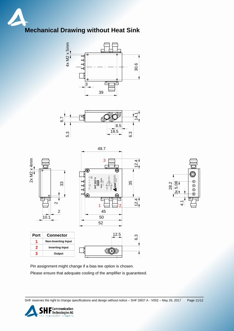
Mechanical Drawing without Heat Sink
Pin assignment might change if a bias tee option is chosen.
Please ensure that adequate cooling of the amplifier is guaranteed.
4542
9
SH
F D
837
A
60kH
z -
35G
Hz
P
: 1
6dB
m
ncI2
Cnc
+9V
0.4A
GN
D
03dB
Com
mu
nica
tion
Tech
nolo
gies
AG
Ger
man
yS
HF
10dB
-+
45
35
52
49.7
50
12.4
12.4
14.1
6.3
8.518.5
6.7
5.3
30.6
6.312.5
4.1
28.2
1 2
3
210.1
233
2x M
2 x
4mm
4x M
2 x
5mm
Port Connector
12
3
Non-Inverting Input
Output
Inverting Input
3x 5
.08
3
39
SHF reserves the right to change specifications and design without notice – SHF D837 A - V002 – May 26, 2017 Page 12/12
User Instructions
ATTENTION!
Electrostatic sensitive GaAs FET amplif ier
1. To prevent damage through static charge build up, cables should be always discharged before connecting them to the amplifier!
2. Attach a 50 Ohm output load before supplying DC power to the amplifier!
3. The supply voltage can be taken from any regular 8…12 V, 0.4 A DC power supply and can be connected to the supply feed-through filter via an ON / OFF switch.
4. Using a 3 dB or 6 dB input attenuator will result in a 6 dB or 12 dB increase of the input return loss. For minimal degradation of amplifier rise time, these attenuators should have a bandwidth specification of greater 50 GHz (V/ 1.85mm attenuators)!
5. A differential input signal of about 1 Vpp will produce output swing of about 3 Vpp.
6. Higher input voltages will drive the amplifier’s output stage into saturation, leading to waveform peak clipping.
7. Saturated output voltages can only be used without damage while the amplifier is connected to a 50 Ohm precision load with a VSWR of less than 1.2 or better than 20 dB return loss up to 40 GHz.
8. While using a reflective load the output voltage has to be reduced to a safe operating level according to the magnitudes of the reflections.
9. ATTENTION: At radio frequencies a capacitive load can be transformed to an inductive one through transmission lines! With an output stage driven into saturation this may lead to the immediate destruction of the amplifier (within a few ps)!
10. The input voltage (single ended) should never be greater than 2 Vpp equivalent to 10 dBm input power.