DATASHEET SEARCH SITE | . General description The PCA8574/74A provide general purpose remote I/O...
27
1. General description The PCA8574/74A provide general purpose remote I/O expansion for most microcontroller families via the two-line bidirectional I 2 C-bus (serial clock (SCL), serial data (SDA)). The devices consist of an 8-bit quasi-bidirectional port and an I 2 C-bus interface. The PCA8574/74A have low current consumption and include latched outputs with 25 mA high current drive capability for directly driving LEDs. The PCA8574/74A also possess an interrupt line ( INT) that can be connected to the interrupt logic of the microcontroller. By sending an interrupt signal on this line, the remote I/O can inform the microcontroller if there is incoming data on its ports without having to communicate via the I 2 C-bus. The internal Power-On Reset (POR) initializes the I/Os as inputs. 2. Features ■ 400 kHz I 2 C-bus interface ■ 2.3 V to 5.5 V operation with 5.5 V tolerant I/Os ■ 8-bit remote I/O pins that default to inputs at power-up ■ Latched outputs with 25 mA sink capability for directly driving LEDs ■ Total package sink capability of 200 mA ■ Active LOW open-drain interrupt output ■ 8 programmable slave addresses using 3 address pins ■ Readable device ID (manufacturer, device type, and revision) ■ Low standby current (10 μA max.) ■ -40 °C to +85 °C operation ■ ESD protection exceeds 2000 V HBM per JESD22-A114, 200 V MM per JESD22-A115, and 1000 V CDM per JESD22-C101 ■ Latch-up testing is done to JEDEC standard JESD78 which exceeds 100 mA ■ Packages offered: DIP16, SO16, TSSOP16, SSOP20 3. Applications ■ LED signs and displays ■ Servers ■ Industrial control ■ Medical equipment ■ PLCs PCA8574/74A Remote 8-bit I/O expander for I 2 C-bus with interrupt Rev. 02 — 14 May 2007 Product data sheet
Transcript of DATASHEET SEARCH SITE | . General description The PCA8574/74A provide general purpose remote I/O...
1. General description
The PCA8574/74A provide general purpose remote I/O expansion for mostmicrocontroller families via the two-line bidirectional I2C-bus (serial clock (SCL), serialdata (SDA)).
The devices consist of an 8-bit quasi-bidirectional port and an I2C-bus interface. ThePCA8574/74A have low current consumption and include latched outputs with 25 mA highcurrent drive capability for directly driving LEDs.
The PCA8574/74A also possess an interrupt line (INT) that can be connected to theinterrupt logic of the microcontroller. By sending an interrupt signal on this line, the remoteI/O can inform the microcontroller if there is incoming data on its ports without having tocommunicate via the I2C-bus.
The internal Power-On Reset (POR) initializes the I/Os as inputs.
2. Features
n 400 kHz I2C-bus interface
n 2.3 V to 5.5 V operation with 5.5 V tolerant I/Os
n 8-bit remote I/O pins that default to inputs at power-up
n Latched outputs with 25 mA sink capability for directly driving LEDs
n Total package sink capability of 200 mA
n Active LOW open-drain interrupt output
n 8 programmable slave addresses using 3 address pins
n Readable device ID (manufacturer, device type, and revision)
n Low standby current (10 µA max.)
n −40 °C to +85 °C operation
n ESD protection exceeds 2000 V HBM per JESD22-A114, 200 V MM perJESD22-A115, and 1000 V CDM per JESD22-C101
n Latch-up testing is done to JEDEC standard JESD78 which exceeds 100 mA
n Packages offered: DIP16, SO16, TSSOP16, SSOP20
3. Applications
n LED signs and displays
n Servers
n Industrial control
n Medical equipment
n PLCs
PCA8574/74ARemote 8-bit I/O expander for I 2C-bus with interruptRev. 02 — 14 May 2007 Product data sheet
NXP Semiconductors PCA8574/74ARemote 8-bit I/O expander for I 2C-bus with interrupt
n Cellular telephones
n Gaming machines
n Instrumentation and test measurement
4. Ordering information
5. Block diagram
Table 1. Ordering information
Type number Topsidemark
Package
Name Description Version
PCA8574D PCA8574D SO16 plastic small outline package; 16 leads; body width 7.5 mm SOT162-1
PCA8574AD PCA8574AD
PCA8574N PCA8574N DIP16 plastic dual in-line package; 16 leads (300 mil); long body SOT38-1
PCA8574AN PCA8574AN
PCA8574PW PCA8574 TSSOP16 plastic thin shrink small outline package; 16 leads;body width 4.4 mm
SOT403-1
PCA8574APW PA8574A
PCA8574TS PCA8574 SSOP20 plastic shrink small outline package; 20 leads;body width 4.4 mm
SOT266-1
PCA8574ATS PCA8574A
Fig 1. Block diagram of PCA8574/74A
002aac677
INT
I2C-BUSCONTROL
INTERRUPTLOGIC
PCA8574PCA8574A
LP FILTER
AD0AD1AD2
INPUTFILTER
SHIFTREGISTER
SDA
SCL8 BITS
write pulseread pulse
POWER-ONRESETVDD
VSS
I/OPORT P0 to P7
PCA8574_PCA8574A_2 © NXP B.V. 2007. All rights reserved.
Product data sheet Rev. 02 — 14 May 2007 2 of 27
NXP Semiconductors PCA8574/74ARemote 8-bit I/O expander for I 2C-bus with interrupt
6. Pinning information
6.1 Pinning
Fig 2. Simplified schematic diagram of P0 to P7
002aac109
write pulse
read pulse
D
CIS
FF
Q
power-on reset
data from Shift Register
Itrt(pu)
100 µAIOH
IOL
VDD
P0 to P7
VSS
D
CIS
FF
Q
data to Shift Register to interrupt logic
Fig 3. Pin configuration for DIP16 Fig 4. Pin configuration for SO16
PCA8574NPCA8574AN
AD0 VDD
AD1 SDA
AD2 SCL
P0 INT
P1 P7
P2 P6
P3 P5
VSS P4
002aac679
1
2
3
4
5
6
7
8
10
9
12
11
14
13
16
15
PCA8574DPCA8574AD
AD0 VDD
AD1 SDA
AD2 SCL
P0 INT
P1 P7
P2 P6
P3 P5
VSS P4
002aac678
1
2
3
4
5
6
7
8
10
9
12
11
14
13
16
15
PCA8574_PCA8574A_2 © NXP B.V. 2007. All rights reserved.
Product data sheet Rev. 02 — 14 May 2007 3 of 27
NXP Semiconductors PCA8574/74ARemote 8-bit I/O expander for I 2C-bus with interrupt
6.2 Pin description
Fig 5. Pin configuration for TSSOP16 Fig 6. Pin configuration for SSOP20
PCA8574PWPCA8574APW
AD0 VDD
AD1 SDA
AD2 SCL
P0 INT
P1 P7
P2 P6
P3 P5
VSS P4
002aac941
1
2
3
4
5
6
7
8
10
9
12
11
14
13
16
15
PCA8574TSPCA8574ATS
INT P7
SCL P6
n.c. n.c.
SDA P5
VDD P4
AD0 VSS
AD1 P3
n.c. n.c.
AD2 P2
P0 P1
002aac680
1
2
3
4
5
6
7
8
9
10
12
11
14
13
16
15
18
17
20
19
Table 2. Pin description for DIP16, SO16, TSSOP16
Symbol Pin Description
AD0 1 address input 0
AD1 2 address input 1
AD2 3 address input 2
P0 4 quasi-bidirectional I/O 0
P1 5 quasi-bidirectional I/O 1
P2 6 quasi-bidirectional I/O 2
P3 7 quasi-bidirectional I/O 3
VSS 8 supply ground
P4 9 quasi-bidirectional I/O 4
P5 10 quasi-bidirectional I/O 5
P6 11 quasi-bidirectional I/O 6
P7 12 quasi-bidirectional I/O 7
INT 13 interrupt output (active LOW)
SCL 14 serial clock line
SDA 15 serial data line
VDD 16 supply voltage
PCA8574_PCA8574A_2 © NXP B.V. 2007. All rights reserved.
Product data sheet Rev. 02 — 14 May 2007 4 of 27
NXP Semiconductors PCA8574/74ARemote 8-bit I/O expander for I 2C-bus with interrupt
Table 3. Pin description for SSOP20
Symbol Pin Description
INT 1 interrupt output (active LOW)
SCL 2 serial clock line
n.c. 3 not connected
SDA 4 serial data line
VDD 5 supply voltage
AD0 6 address input 0
AD1 7 address input 1
n.c. 8 not connected
AD2 9 address input 2
P0 10 quasi-bidirectional I/O 0
P1 11 quasi-bidirectional I/O 1
P2 12 quasi-bidirectional I/O 2
n.c. 13 not connected
P3 14 quasi-bidirectional I/O 3
VSS 15 supply ground
P4 16 quasi-bidirectional I/O 4
P5 17 quasi-bidirectional I/O 5
n.c. 18 not connected
P6 19 quasi-bidirectional I/O 6
P7 20 quasi-bidirectional I/O 7
PCA8574_PCA8574A_2 © NXP B.V. 2007. All rights reserved.
Product data sheet Rev. 02 — 14 May 2007 5 of 27
NXP Semiconductors PCA8574/74ARemote 8-bit I/O expander for I 2C-bus with interrupt
7. Functional description
Refer to Figure 1 “Block diagram of PCA8574/74A”.
7.1 Device addressFollowing a START condition, the bus master must send the address of the slave it isaccessing and the operation it wants to perform (read or write). The address of thePCA8574/74A is shown in Figure 7. Slave address pins AD2, AD1, and AD0 choose 1 of8 slave addresses. To conserve power, no internal pull-up resistors are incorporated onAD2, AD1, and AD0. Address values depending on AD2, AD1, and AD0 can be found inTable 4 “PCA8574 address map” and Table 5 “PCA8574A address map”.
Remark: When using the PCA8574A, the General Call address (0000 0000b) and theDevice ID address (1111 100Xb) are reserved and cannot be used as device address.Failure to follow this requirement will cause the PCA8574A not to acknowledge.
The last bit of the first byte defines the operation to be performed. When set to logic 1 aread is selected, while a logic 0 selects a write operation.
When AD2, AD1 and AD0 are held to VDD or VSS, the same address as the PCF8574 orPCF8574A is applied.
7.1.1 Address maps
Fig 7. PCA8574/74A address
R/W
002aab636
A6 A5 A4 A3 A2 A1 A0
programmable
slave address
Table 4. PCA8574 address map
A6 A5 A4 A3 A2 A1 A0 Address
0 1 0 0 0 0 0 20h
0 1 0 0 0 0 1 21h
0 1 0 0 0 1 0 22h
0 1 0 0 0 1 1 23h
0 1 0 0 1 0 0 24h
0 1 0 0 1 0 1 25h
0 1 0 0 1 1 0 26h
0 1 0 0 1 1 1 27h
PCA8574_PCA8574A_2 © NXP B.V. 2007. All rights reserved.
Product data sheet Rev. 02 — 14 May 2007 6 of 27
NXP Semiconductors PCA8574/74ARemote 8-bit I/O expander for I 2C-bus with interrupt
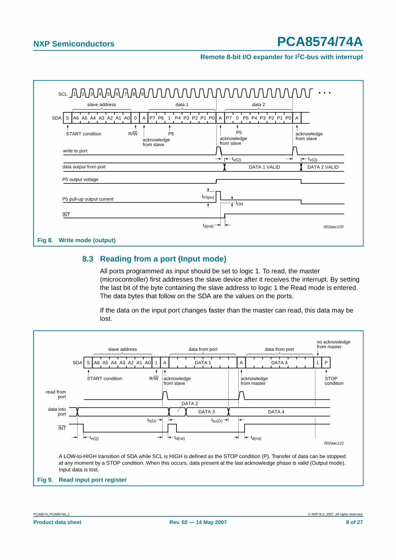
8. I/O programming
8.1 Quasi-bidirectional I/O architectureThe PCA8574/74A’s 8 ports (see Figure 2) are entirely independent and can be usedeither as input or output ports. Input data is transferred from the ports to themicrocontroller in the Read mode (see Figure 9). Output data is transmitted to the ports inthe Write mode (see Figure 8).
This quasi-bidirectional I/O can be used as an input or output without the use of a controlsignal for data directions. At power-on the I/Os are HIGH. In this mode only a currentsource (IOH) to VDD is active. An additional strong pull-up to VDD (Itrt(pu)) allows fast risingedges into heavily loaded outputs. These devices turn on when an output is written HIGH,and are switched off by the negative edge of SCL. The I/Os should be HIGH before beingused as inputs. After power-on, as all the I/Os are set HIGH, all of them can be used asinputs. Any change in setting of the I/Os as either inputs or outputs can be done with thewrite mode.
Remark: If a HIGH is applied to an I/O which has been written earlier to LOW, a largecurrent (IOL) will flow to VSS.
8.2 Writing to the port (Output mode)To write, the master (microcontroller) first addresses the slave device. By setting the lastbit of the byte containing the slave address to logic 0 the write mode is entered. ThePCA8574/74A acknowledges and the master sends the data byte for P7 to P0 and isacknowledged by the PCA8574/74A. The 8-bit data is presented on the port lines after ithas been acknowledged by the PCA8574/74A.
The number of data bytes that can be sent successively is not limited. The previous datais overwritten every time a data byte has been sent.
Table 5. PCA8574A address map
A6 A5 A4 A3 A2 A1 A0 Address
0 1 1 1 0 0 0 38h
0 1 1 1 0 0 1 39h
0 1 1 1 0 1 0 3Ah
0 1 1 1 0 1 1 3Bh
0 1 1 1 1 0 0 3Ch
0 1 1 1 1 0 1 3Dh
0 1 1 1 1 1 0 3Eh
0 1 1 1 1 1 1 3Fh
PCA8574_PCA8574A_2 © NXP B.V. 2007. All rights reserved.
Product data sheet Rev. 02 — 14 May 2007 7 of 27
NXP Semiconductors PCA8574/74ARemote 8-bit I/O expander for I 2C-bus with interrupt
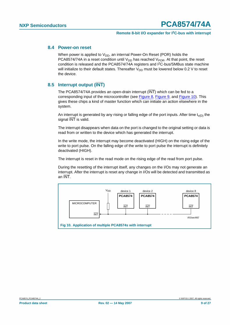
8.3 Reading from a port (Input mode)All ports programmed as input should be set to logic 1. To read, the master(microcontroller) first addresses the slave device after it receives the interrupt. By settingthe last bit of the byte containing the slave address to logic 1 the Read mode is entered.The data bytes that follow on the SDA are the values on the ports.
If the data on the input port changes faster than the master can read, this data may belost.
Fig 8. Write mode (output)
A5 A4 A3 A2 A1 A0 0 AS A6
slave address
START condition R/Wacknowledgefrom slave
002aac120
P6 1P7
data 1
A
acknowledgefrom slave
1 2 3 4 5 6 7 8SCL 9
SDA A
acknowledgefrom slave
write to port
data output from port
tv(Q)
P5
data 2
DATA 2 VALID
P4 P3 P2 P1 P0 P7 P4 P3 P2 P1 P00
P5
P5
tv(Q)
DATA 1 VALID
P5 output voltage
Itrt(pu)
IOHP5 pull-up output current
td(rst)
INT
A LOW-to-HIGH transition of SDA while SCL is HIGH is defined as the STOP condition (P). Transfer of data can be stoppedat any moment by a STOP condition. When this occurs, data present at the last acknowledge phase is valid (Output mode).Input data is lost.
Fig 9. Read input port register
A5 A4 A3 A2 A1 A0 1 AS A6
slave address
START condition R/W acknowledgefrom slave
002aac121
data from port
A
acknowledgefrom master
SDA 1
no acknowledgefrom master
read fromport
data intoport
data from port
DATA 1
DATA 4
INT
DATA 4
DATA 2
DATA 3
P
STOPcondition
tv(Q) td(rst)
th(D) tsu(D)
td(rst)
PCA8574_PCA8574A_2 © NXP B.V. 2007. All rights reserved.
Product data sheet Rev. 02 — 14 May 2007 8 of 27
NXP Semiconductors PCA8574/74ARemote 8-bit I/O expander for I 2C-bus with interrupt
8.4 Power-on resetWhen power is applied to VDD, an internal Power-On Reset (POR) holds thePCA8574/74A in a reset condition until VDD has reached VPOR. At that point, the resetcondition is released and the PCA8574/74A registers and I2C-bus/SMBus state machinewill initialize to their default states. Thereafter VDD must be lowered below 0.2 V to resetthe device.
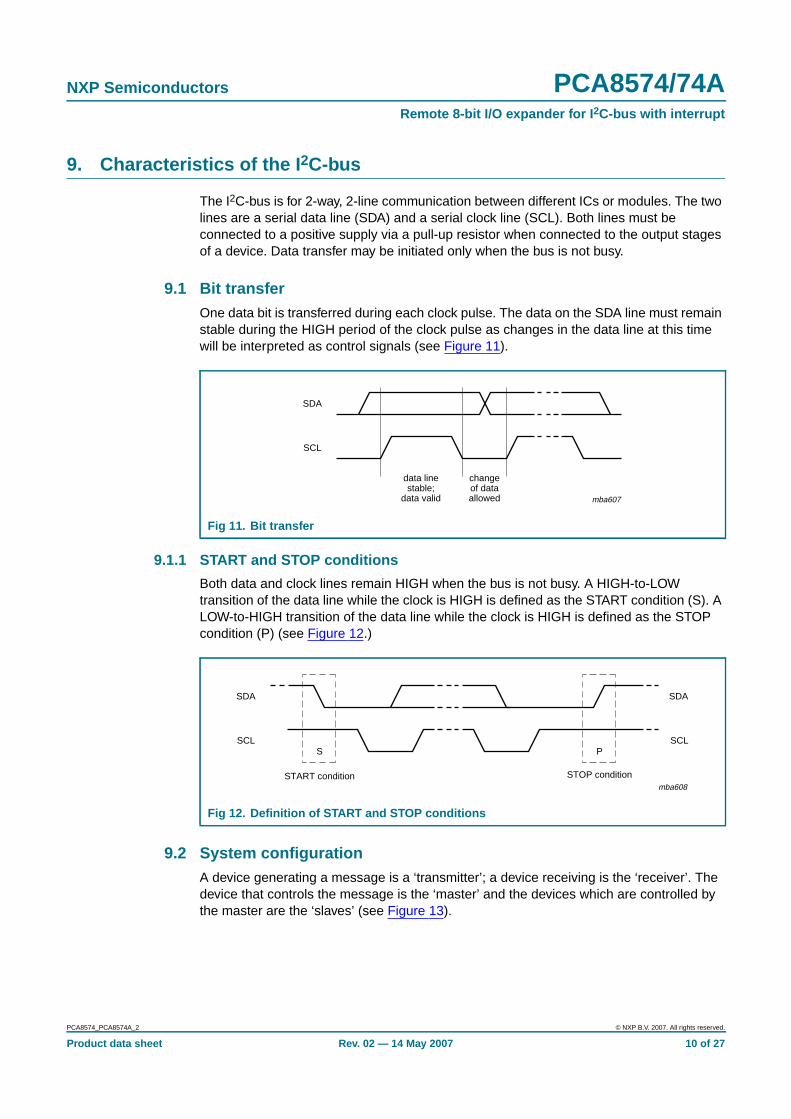
8.5 Interrupt output ( INT)The PCA8574/74A provides an open-drain interrupt (INT) which can be fed to acorresponding input of the microcontroller (see Figure 8, Figure 9, and Figure 10). Thisgives these chips a kind of master function which can initiate an action elsewhere in thesystem.
An interrupt is generated by any rising or falling edge of the port inputs. After time tv(D) thesignal INT is valid.
The interrupt disappears when data on the port is changed to the original setting or data isread from or written to the device which has generated the interrupt.
In the write mode, the interrupt may become deactivated (HIGH) on the rising edge of thewrite to port pulse. On the falling edge of the write to port pulse the interrupt is definitelydeactivated (HIGH).
The interrupt is reset in the read mode on the rising edge of the read from port pulse.
During the resetting of the interrupt itself, any changes on the I/Os may not generate aninterrupt. After the interrupt is reset any change in I/Os will be detected and transmitted asan INT.
Fig 10. Application of multiple PCA8574s with interrupt
002aac682
VDD
MICROCOMPUTER
INT
PCA8574
INT
PCA8574
INT
device 1 device 2
PCA8574
INT
device 8
PCA8574_PCA8574A_2 © NXP B.V. 2007. All rights reserved.
Product data sheet Rev. 02 — 14 May 2007 9 of 27
NXP Semiconductors PCA8574/74ARemote 8-bit I/O expander for I 2C-bus with interrupt
9. Characteristics of the I 2C-bus
The I2C-bus is for 2-way, 2-line communication between different ICs or modules. The twolines are a serial data line (SDA) and a serial clock line (SCL). Both lines must beconnected to a positive supply via a pull-up resistor when connected to the output stagesof a device. Data transfer may be initiated only when the bus is not busy.
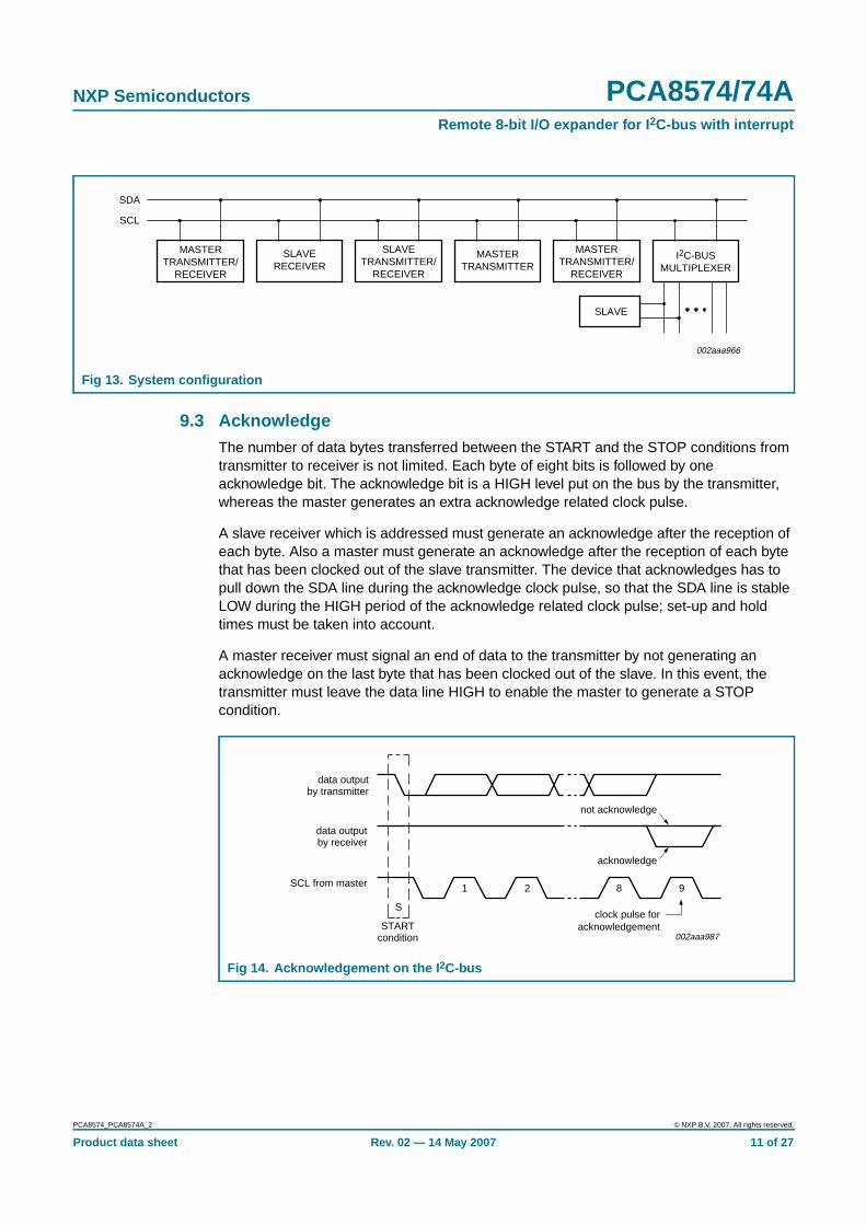
9.1 Bit transferOne data bit is transferred during each clock pulse. The data on the SDA line must remainstable during the HIGH period of the clock pulse as changes in the data line at this timewill be interpreted as control signals (see Figure 11).
9.1.1 START and STOP conditions
Both data and clock lines remain HIGH when the bus is not busy. A HIGH-to-LOWtransition of the data line while the clock is HIGH is defined as the START condition (S). ALOW-to-HIGH transition of the data line while the clock is HIGH is defined as the STOPcondition (P) (see Figure 12.)
9.2 System configurationA device generating a message is a ‘transmitter’; a device receiving is the ‘receiver’. Thedevice that controls the message is the ‘master’ and the devices which are controlled bythe master are the ‘slaves’ (see Figure 13).
Fig 11. Bit transfer
mba607
data linestable;
data valid
changeof dataallowed
SDA
SCL
Fig 12. Definition of START and STOP conditions
mba608
SDA
SCLP
STOP condition
SDA
SCLS
START condition
PCA8574_PCA8574A_2 © NXP B.V. 2007. All rights reserved.
Product data sheet Rev. 02 — 14 May 2007 10 of 27
NXP Semiconductors PCA8574/74ARemote 8-bit I/O expander for I 2C-bus with interrupt
9.3 AcknowledgeThe number of data bytes transferred between the START and the STOP conditions fromtransmitter to receiver is not limited. Each byte of eight bits is followed by oneacknowledge bit. The acknowledge bit is a HIGH level put on the bus by the transmitter,whereas the master generates an extra acknowledge related clock pulse.
A slave receiver which is addressed must generate an acknowledge after the reception ofeach byte. Also a master must generate an acknowledge after the reception of each bytethat has been clocked out of the slave transmitter. The device that acknowledges has topull down the SDA line during the acknowledge clock pulse, so that the SDA line is stableLOW during the HIGH period of the acknowledge related clock pulse; set-up and holdtimes must be taken into account.
A master receiver must signal an end of data to the transmitter by not generating anacknowledge on the last byte that has been clocked out of the slave. In this event, thetransmitter must leave the data line HIGH to enable the master to generate a STOPcondition.
Fig 13. System configuration
002aaa966
MASTERTRANSMITTER/
RECEIVER
SLAVERECEIVER
SLAVETRANSMITTER/
RECEIVER
MASTERTRANSMITTER
MASTERTRANSMITTER/
RECEIVER
SDA
SCL
I2C-BUSMULTIPLEXER
SLAVE
Fig 14. Acknowledgement on the I 2C-bus
002aaa987
S
STARTcondition
9821
clock pulse foracknowledgement
not acknowledge
acknowledge
data outputby transmitter
data outputby receiver
SCL from master
PCA8574_PCA8574A_2 © NXP B.V. 2007. All rights reserved.
Product data sheet Rev. 02 — 14 May 2007 11 of 27
NXP Semiconductors PCA8574/74ARemote 8-bit I/O expander for I 2C-bus with interrupt
10. Application design-in information
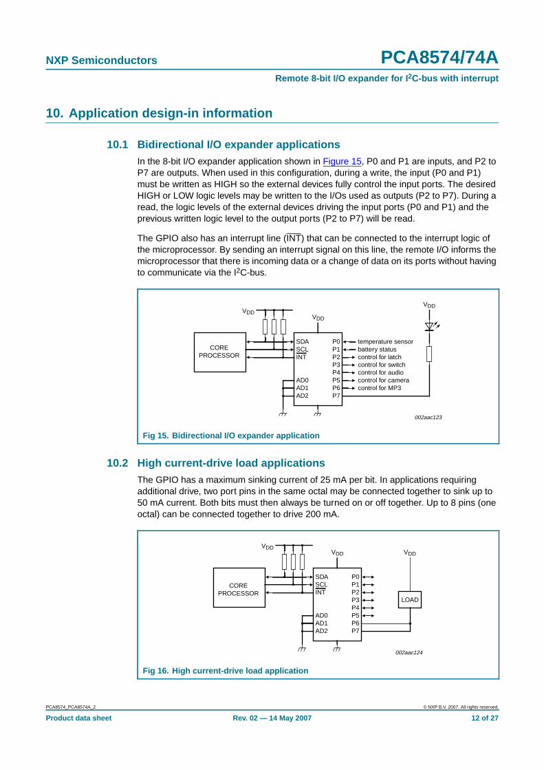
10.1 Bidirectional I/O expander applicationsIn the 8-bit I/O expander application shown in Figure 15, P0 and P1 are inputs, and P2 toP7 are outputs. When used in this configuration, during a write, the input (P0 and P1)must be written as HIGH so the external devices fully control the input ports. The desiredHIGH or LOW logic levels may be written to the I/Os used as outputs (P2 to P7). During aread, the logic levels of the external devices driving the input ports (P0 and P1) and theprevious written logic level to the output ports (P2 to P7) will be read.
The GPIO also has an interrupt line (INT) that can be connected to the interrupt logic ofthe microprocessor. By sending an interrupt signal on this line, the remote I/O informs themicroprocessor that there is incoming data or a change of data on its ports without havingto communicate via the I2C-bus.
10.2 High current-drive load applicationsThe GPIO has a maximum sinking current of 25 mA per bit. In applications requiringadditional drive, two port pins in the same octal may be connected together to sink up to50 mA current. Both bits must then always be turned on or off together. Up to 8 pins (oneoctal) can be connected together to drive 200 mA.
Fig 15. Bidirectional I/O expander application
002aac123
VDD
temperature sensorbattery statuscontrol for latchcontrol for switchcontrol for audiocontrol for cameracontrol for MP3
P0P1P2P3P4P5P6P7
VDD
SDASCLINT
AD0AD1AD2
COREPROCESSOR
VDD
Fig 16. High current-drive load application
002aac124
VDD
P0P1P2P3P4P5P6P7
VDD
SDASCLINT
AD0AD1AD2
COREPROCESSOR
VDD
LOAD
PCA8574_PCA8574A_2 © NXP B.V. 2007. All rights reserved.
Product data sheet Rev. 02 — 14 May 2007 12 of 27
NXP Semiconductors PCA8574/74ARemote 8-bit I/O expander for I 2C-bus with interrupt
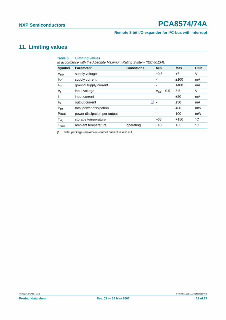
11. Limiting values
[1] Total package (maximum) output current is 400 mA.
Table 6. Limiting valuesIn accordance with the Absolute Maximum Rating System (IEC 60134).
Symbol Parameter Conditions Min Max Unit
VDD supply voltage −0.5 +6 V
IDD supply current - ±100 mA
ISS ground supply current - ±400 mA
VI input voltage VSS − 0.5 5.5 V
II input current - ±20 mA
IO output current [1] - ±50 mA
Ptot total power dissipation - 400 mW
P/out power dissipation per output - 100 mW
Tstg storage temperature −65 +150 °C
Tamb ambient temperature operating −40 +85 °C
PCA8574_PCA8574A_2 © NXP B.V. 2007. All rights reserved.
Product data sheet Rev. 02 — 14 May 2007 13 of 27
NXP Semiconductors PCA8574/74ARemote 8-bit I/O expander for I 2C-bus with interrupt
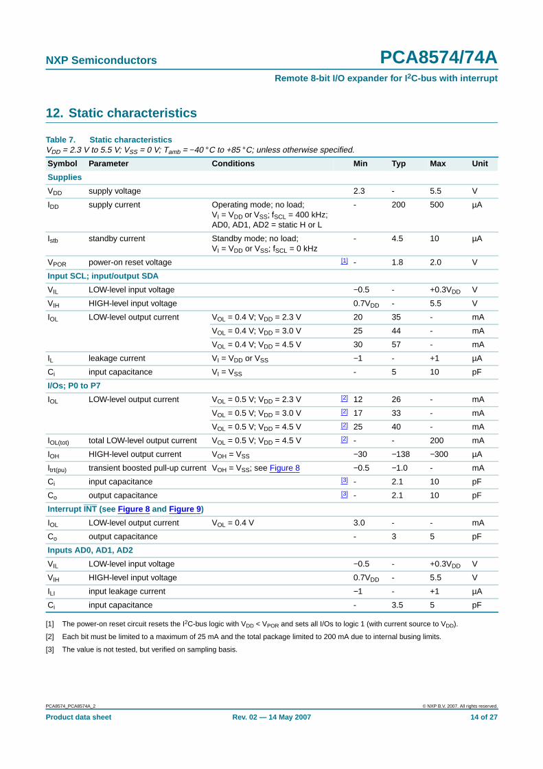
12. Static characteristics
[1] The power-on reset circuit resets the I2C-bus logic with VDD < VPOR and sets all I/Os to logic 1 (with current source to VDD).
[2] Each bit must be limited to a maximum of 25 mA and the total package limited to 200 mA due to internal busing limits.
[3] The value is not tested, but verified on sampling basis.
Table 7. Static characteristicsVDD = 2.3 V to 5.5 V; VSS = 0 V; Tamb = −40 °C to +85 °C; unless otherwise specified.
Symbol Parameter Conditions Min Typ Max Unit
Supplies
VDD supply voltage 2.3 - 5.5 V
IDD supply current Operating mode; no load;VI = VDD or VSS; fSCL = 400 kHz;AD0, AD1, AD2 = static H or L
- 200 500 µA
Istb standby current Standby mode; no load;VI = VDD or VSS; fSCL = 0 kHz
- 4.5 10 µA
VPOR power-on reset voltage [1] - 1.8 2.0 V
Input SCL; input/output SDA
VIL LOW-level input voltage −0.5 - +0.3VDD V
VIH HIGH-level input voltage 0.7VDD - 5.5 V
IOL LOW-level output current VOL = 0.4 V; VDD = 2.3 V 20 35 - mA
VOL = 0.4 V; VDD = 3.0 V 25 44 - mA
VOL = 0.4 V; VDD = 4.5 V 30 57 - mA
IL leakage current VI = VDD or VSS −1 - +1 µA
Ci input capacitance VI = VSS - 5 10 pF
I/Os; P0 to P7
IOL LOW-level output current VOL = 0.5 V; VDD = 2.3 V [2] 12 26 - mA
VOL = 0.5 V; VDD = 3.0 V [2] 17 33 - mA
VOL = 0.5 V; VDD = 4.5 V [2] 25 40 - mA
IOL(tot) total LOW-level output current VOL = 0.5 V; VDD = 4.5 V [2] - - 200 mA
IOH HIGH-level output current VOH = VSS −30 −138 −300 µA
Itrt(pu) transient boosted pull-up current VOH = VSS; see Figure 8 −0.5 −1.0 - mA
Ci input capacitance [3] - 2.1 10 pF
Co output capacitance [3] - 2.1 10 pF
Interrupt INT (see Figure 8 and Figure 9)
IOL LOW-level output current VOL = 0.4 V 3.0 - - mA
Co output capacitance - 3 5 pF
Inputs AD0, AD1, AD2
VIL LOW-level input voltage −0.5 - +0.3VDD V
VIH HIGH-level input voltage 0.7VDD - 5.5 V
ILI input leakage current −1 - +1 µA
Ci input capacitance - 3.5 5 pF
PCA8574_PCA8574A_2 © NXP B.V. 2007. All rights reserved.
Product data sheet Rev. 02 — 14 May 2007 14 of 27
NXP Semiconductors PCA8574/74ARemote 8-bit I/O expander for I 2C-bus with interrupt
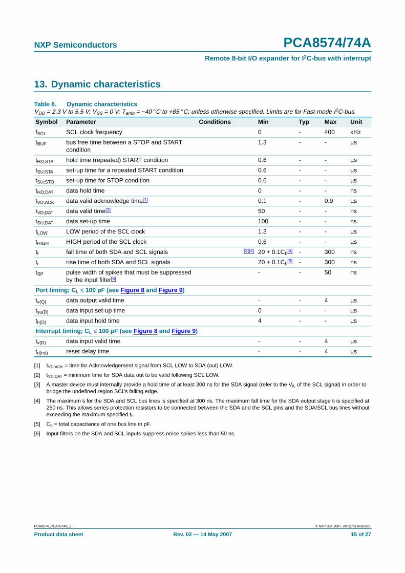
13. Dynamic characteristics
[1] tVD;ACK = time for Acknowledgement signal from SCL LOW to SDA (out) LOW.
[2] tVD;DAT = minimum time for SDA data out to be valid following SCL LOW.
[3] A master device must internally provide a hold time of at least 300 ns for the SDA signal (refer to the VIL of the SCL signal) in order tobridge the undefined region SCL’s falling edge.
[4] The maximum tf for the SDA and SCL bus lines is specified at 300 ns. The maximum fall time for the SDA output stage tf is specified at250 ns. This allows series protection resistors to be connected between the SDA and the SCL pins and the SDA/SCL bus lines withoutexceeding the maximum specified tf.
[5] Cb = total capacitance of one bus line in pF.
[6] Input filters on the SDA and SCL inputs suppress noise spikes less than 50 ns.
Table 8. Dynamic characteristicsVDD = 2.3 V to 5.5 V; VSS = 0 V; Tamb = −40 °C to +85 °C; unless otherwise specified. Limits are for Fast-mode I2C-bus.
Symbol Parameter Conditions Min Typ Max Unit
fSCL SCL clock frequency 0 - 400 kHz
tBUF bus free time between a STOP and STARTcondition
1.3 - - µs
tHD;STA hold time (repeated) START condition 0.6 - - µs
tSU;STA set-up time for a repeated START condition 0.6 - - µs
tSU;STO set-up time for STOP condition 0.6 - - µs
tHD;DAT data hold time 0 - - ns
tVD;ACK data valid acknowledge time[1] 0.1 - 0.9 µs
tVD;DAT data valid time[2] 50 - - ns
tSU;DAT data set-up time 100 - - ns
tLOW LOW period of the SCL clock 1.3 - - µs
tHIGH HIGH period of the SCL clock 0.6 - - µs
tf fall time of both SDA and SCL signals [3][4] 20 + 0.1Cb[5] - 300 ns
tr rise time of both SDA and SCL signals 20 + 0.1Cb[5] - 300 ns
tSP pulse width of spikes that must be suppressedby the input filter[6]
- - 50 ns
Port timing; C L ≤ 100 pF (see Figure 8 and Figure 9)
tv(Q) data output valid time - - 4 µs
tsu(D) data input set-up time 0 - - µs
th(D) data input hold time 4 - - µs
Interrupt timing; C L ≤ 100 pF (see Figure 8 and Figure 9)
tv(D) data input valid time - - 4 µs
td(rst) reset delay time - - 4 µs
PCA8574_PCA8574A_2 © NXP B.V. 2007. All rights reserved.
Product data sheet Rev. 02 — 14 May 2007 15 of 27
NXP Semiconductors PCA8574/74ARemote 8-bit I/O expander for I 2C-bus with interrupt
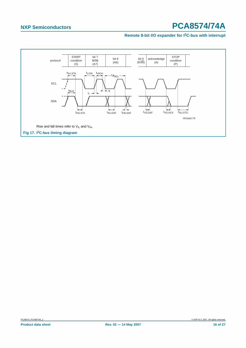
Rise and fall times refer to VIL and VIH.
Fig 17. I2C-bus timing diagram
SCL
SDA
tHD;STA tSU;DAT tHD;DAT
tftBUF
tSU;STA tLOW tHIGH
tVD;ACK
002aab175
tSU;STO
protocolSTART
condition(S)
bit 7MSB(A7)
bit 6(A6)
bit 0(R/W)
acknowledge(A)
STOPcondition
(P)
1/fSCL
tr
tVD;DAT
PCA8574_PCA8574A_2 © NXP B.V. 2007. All rights reserved.
Product data sheet Rev. 02 — 14 May 2007 16 of 27
NXP Semiconductors PCA8574/74ARemote 8-bit I/O expander for I 2C-bus with interrupt
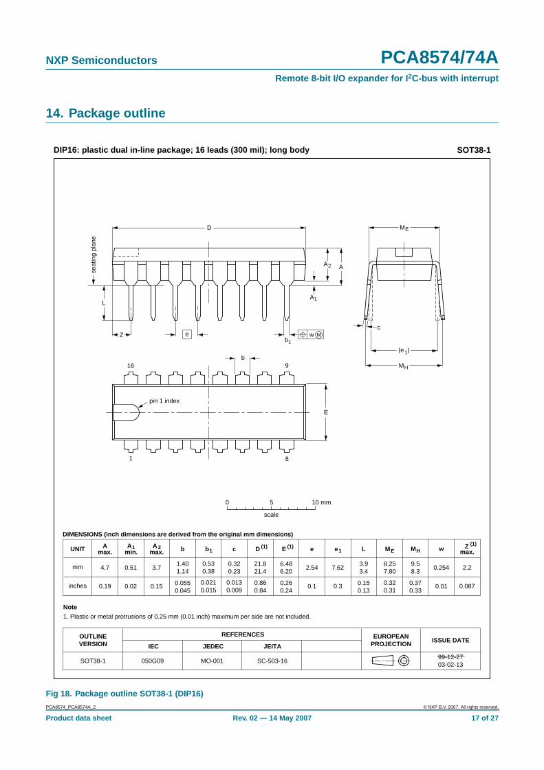
14. Package outline
Fig 18. Package outline SOT38-1 (DIP16)
UNIT Amax.
1 2 b1 c E e MHL
REFERENCESOUTLINEVERSION
EUROPEANPROJECTION ISSUE DATE
IEC JEDEC JEITA
mm
inches
DIMENSIONS (inch dimensions are derived from the original mm dimensions)
SOT38-199-12-2703-02-13
A min.
A max. b max.wMEe1
1.401.14
0.0550.045
0.530.38
0.320.23
21.821.4
0.860.84
6.486.20
0.260.24
3.93.4
0.150.13
0.2542.54 7.62
0.3
8.257.80
0.320.31
9.58.3
0.370.33
2.2
0.087
4.7 0.51 3.7
0.150.0210.015
0.0130.009
0.010.10.020.19
050G09 MO-001 SC-503-16
MH
c
(e )1
ME
A
L
seat
ing
plan
e
A1
w Mb1
e
D
A2
Z
16
1
9
8
b
E
pin 1 index
0 5 10 mm
scale
Note
1. Plastic or metal protrusions of 0.25 mm (0.01 inch) maximum per side are not included.
(1) (1)D(1)Z
DIP16: plastic dual in-line package; 16 leads (300 mil); long body SOT38-1
PCA8574_PCA8574A_2 © NXP B.V. 2007. All rights reserved.
Product data sheet Rev. 02 — 14 May 2007 17 of 27
NXP Semiconductors PCA8574/74ARemote 8-bit I/O expander for I 2C-bus with interrupt
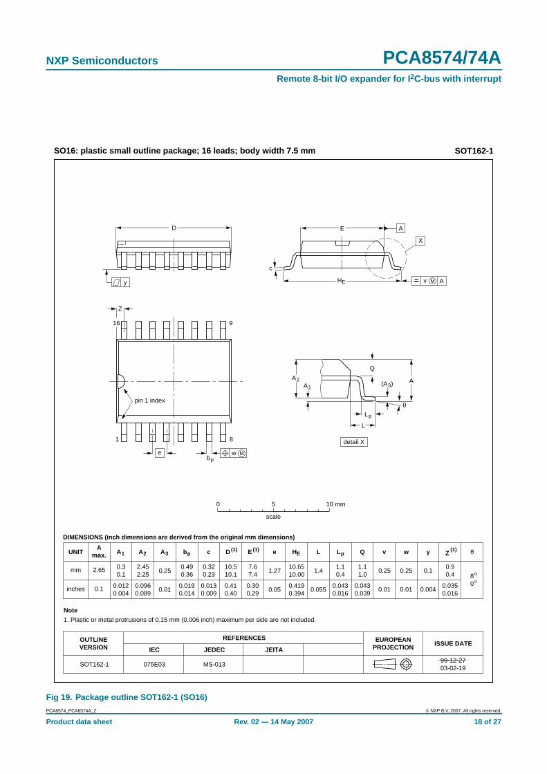
Fig 19. Package outline SOT162-1 (SO16)
UNITA
max. A1 A2 A3 bp c D (1) E (1) (1)e HE L L p Q Zywv θ
REFERENCESOUTLINEVERSION
EUROPEANPROJECTION ISSUE DATE
IEC JEDEC JEITA
mm
inches
2.65 0.30.1
2.452.25
0.490.36
0.320.23
10.510.1
7.67.4
1.2710.6510.00
1.11.0
0.90.4 8
0
o
o
0.25 0.1
DIMENSIONS (inch dimensions are derived from the original mm dimensions)
Note
1. Plastic or metal protrusions of 0.15 mm (0.006 inch) maximum per side are not included.
1.10.4
SOT162-1
8
16
w Mbp
D
detail X
Z
e
9
1
y
0.25
075E03 MS-013
pin 1 index
0.1 0.0120.004
0.0960.089
0.0190.014
0.0130.009
0.410.40
0.300.29
0.05
1.4
0.0550.4190.394
0.0430.039
0.0350.016
0.01
0.25
0.01 0.0040.0430.016
0.01
X
θ
AA1
A2
HE
Lp
Q
E
c
L
v M A
(A )3
A
0 5 10 mm
scale
SO16: plastic small outline package; 16 leads; body width 7.5 mm SOT162-1
99-12-2703-02-19
PCA8574_PCA8574A_2 © NXP B.V. 2007. All rights reserved.
Product data sheet Rev. 02 — 14 May 2007 18 of 27

NXP Semiconductors PCA8574/74ARemote 8-bit I/O expander for I 2C-bus with interrupt
Fig 20. Package outline SOT403-1 (TSSOP16)
UNIT A1 A2 A3 bp c D (1) E (2) (1)e HE L L p Q Zywv θ
REFERENCESOUTLINEVERSION
EUROPEANPROJECTION ISSUE DATE
IEC JEDEC JEITA
mm 0.150.05
0.950.80
0.300.19
0.20.1
5.14.9
4.54.3
0.656.66.2
0.40.3
0.400.06
80
o
o0.13 0.10.21
DIMENSIONS (mm are the original dimensions)
Notes
1. Plastic or metal protrusions of 0.15 mm maximum per side are not included.
2. Plastic interlead protrusions of 0.25 mm maximum per side are not included.
0.750.50
SOT403-1 MO-15399-12-2703-02-18
w Mbp
D
Z
e
0.25
1 8
16 9
θ
AA1
A2
Lp
Q
detail X
L
(A )3
HE
E
c
v M A
XA
y
0 2.5 5 mm
scale
TSSOP16: plastic thin shrink small outline package; 16 leads; body width 4.4 mm SOT403-1
Amax.
1.1
pin 1 index
PCA8574_PCA8574A_2 © NXP B.V. 2007. All rights reserved.
Product data sheet Rev. 02 — 14 May 2007 19 of 27
NXP Semiconductors PCA8574/74ARemote 8-bit I/O expander for I 2C-bus with interrupt
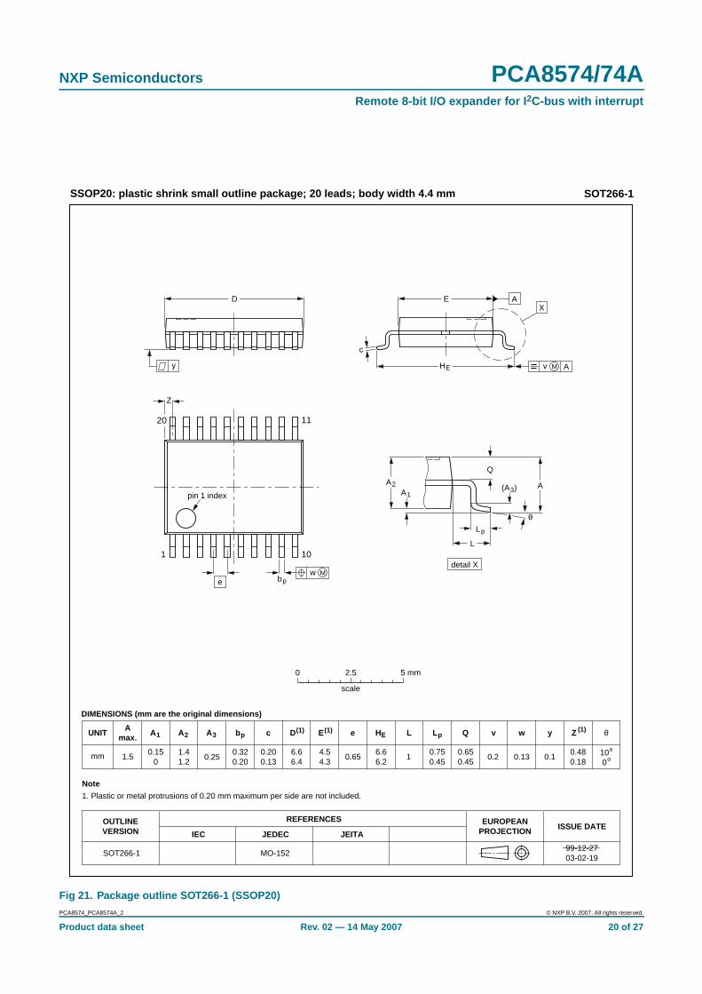
Fig 21. Package outline SOT266-1 (SSOP20)
UNIT A1 A2 A3 bp c D(1) E(1) (1)e HE L L p Q Zywv θ
REFERENCESOUTLINEVERSION
EUROPEANPROJECTION ISSUE DATE
IEC JEDEC JEITA
mm 0.150
1.41.2
0.320.20
0.200.13
6.66.4
4.54.3
0.65 1 0.26.66.2
0.650.45
0.480.18
100
o
o0.13 0.1
DIMENSIONS (mm are the original dimensions)
Note
1. Plastic or metal protrusions of 0.20 mm maximum per side are not included.
0.750.45
SOT266-1 MO-15299-12-2703-02-19
w M
θ
AA1
A2
bp
D
HE
Lp
Q
detail X
E
Z
e
c
L
v M A
X
(A )3
A
y
0.25
1 10
20 11
pin 1 index
0 2.5 5 mm
scale
SSOP20: plastic shrink small outline package; 20 leads; body width 4.4 mm SOT266-1
Amax.
1.5
PCA8574_PCA8574A_2 © NXP B.V. 2007. All rights reserved.
Product data sheet Rev. 02 — 14 May 2007 20 of 27
NXP Semiconductors PCA8574/74ARemote 8-bit I/O expander for I 2C-bus with interrupt
15. Handling information
Inputs and outputs are protected against electrostatic discharge in normal handling.However, to be completely safe you must take normal precautions appropriate to handlingintegrated circuits.
16. Soldering
16.1 IntroductionThere is no soldering method that is ideal for all surface mount IC packages. Wavesoldering can still be used for certain surface mount ICs, but it is not suitable for fine pitchSMDs. In these situations reflow soldering is recommended.
16.2 Through-hole mount packages
16.2.1 Soldering by dipping or by solder wave
Typical dwell time of the leads in the wave ranges from 3 seconds to 4 seconds at 250 °Cor 265 °C, depending on solder material applied, SnPb or Pb-free respectively.
The total contact time of successive solder waves must not exceed 5 seconds.
The device may be mounted up to the seating plane, but the temperature of the plasticbody must not exceed the specified maximum storage temperature (Tstg(max)). If theprinted-circuit board has been pre-heated, forced cooling may be necessary immediatelyafter soldering to keep the temperature within the permissible limit.
16.2.2 Manual soldering
Apply the soldering iron (24 V or less) to the lead(s) of the package, either below theseating plane or not more than 2 mm above it. If the temperature of the soldering iron bit isless than 300 °C it may remain in contact for up to 10 seconds. If the bit temperature isbetween 300 °C and 400 °C, contact may be up to 5 seconds.
16.3 Surface mount packages
16.3.1 Reflow soldering
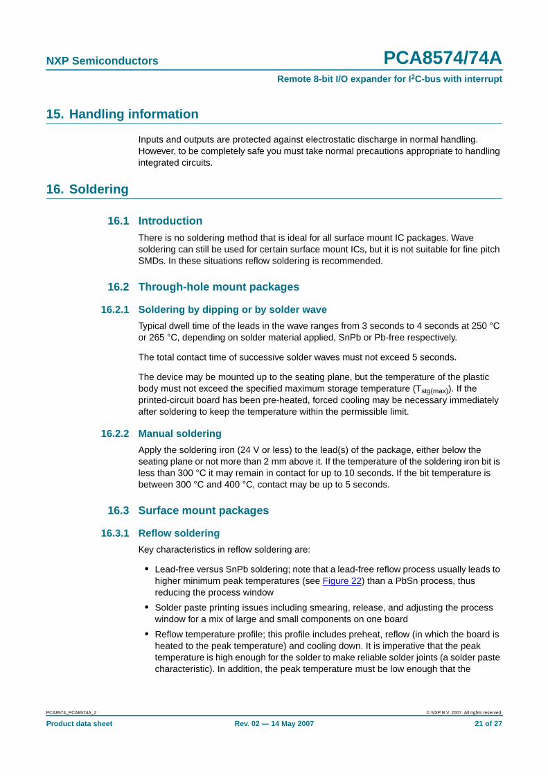
Key characteristics in reflow soldering are:
• Lead-free versus SnPb soldering; note that a lead-free reflow process usually leads tohigher minimum peak temperatures (see Figure 22) than a PbSn process, thusreducing the process window
• Solder paste printing issues including smearing, release, and adjusting the processwindow for a mix of large and small components on one board
• Reflow temperature profile; this profile includes preheat, reflow (in which the board isheated to the peak temperature) and cooling down. It is imperative that the peaktemperature is high enough for the solder to make reliable solder joints (a solder pastecharacteristic). In addition, the peak temperature must be low enough that the
PCA8574_PCA8574A_2 © NXP B.V. 2007. All rights reserved.
Product data sheet Rev. 02 — 14 May 2007 21 of 27
NXP Semiconductors PCA8574/74ARemote 8-bit I/O expander for I 2C-bus with interrupt
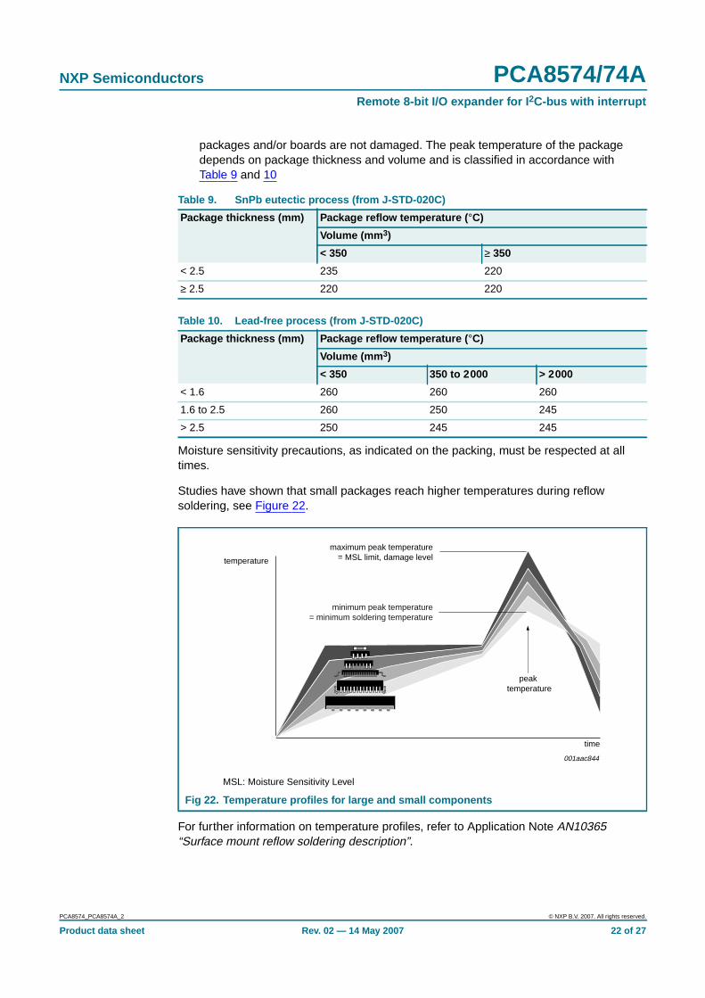
packages and/or boards are not damaged. The peak temperature of the packagedepends on package thickness and volume and is classified in accordance withTable 9 and 10
Moisture sensitivity precautions, as indicated on the packing, must be respected at alltimes.
Studies have shown that small packages reach higher temperatures during reflowsoldering, see Figure 22.
For further information on temperature profiles, refer to Application Note AN10365“Surface mount reflow soldering description”.
Table 9. SnPb eutectic process (from J-STD-020C)
Package thickness (mm) Package reflow temperature ( °C)
Volume (mm 3)
< 350 ≥ 350
< 2.5 235 220
≥ 2.5 220 220
Table 10. Lead-free process (from J-STD-020C)
Package thickness (mm) Package reflow temperature ( °C)
Volume (mm 3)
< 350 350 to 2000 > 2000
< 1.6 260 260 260
1.6 to 2.5 260 250 245
> 2.5 250 245 245
MSL: Moisture Sensitivity Level
Fig 22. Temperature profiles for large and small components
001aac844
temperature
time
minimum peak temperature= minimum soldering temperature
maximum peak temperature= MSL limit, damage level
peak temperature
PCA8574_PCA8574A_2 © NXP B.V. 2007. All rights reserved.
Product data sheet Rev. 02 — 14 May 2007 22 of 27
NXP Semiconductors PCA8574/74ARemote 8-bit I/O expander for I 2C-bus with interrupt
16.3.2 Wave soldering
Conventional single wave soldering is not recommended for surface mount devices(SMDs) or printed-circuit boards with a high component density, as solder bridging andnon-wetting can present major problems.
To overcome these problems the double-wave soldering method was specificallydeveloped.
If wave soldering is used the following conditions must be observed for optimal results:
• Use a double-wave soldering method comprising a turbulent wave with high upwardpressure followed by a smooth laminar wave.
• For packages with leads on two sides and a pitch (e):
– larger than or equal to 1.27 mm, the footprint longitudinal axis is preferred to beparallel to the transport direction of the printed-circuit board;
– smaller than 1.27 mm, the footprint longitudinal axis must be parallel to thetransport direction of the printed-circuit board.
The footprint must incorporate solder thieves at the downstream end.
• For packages with leads on four sides, the footprint must be placed at a 45° angle tothe transport direction of the printed-circuit board. The footprint must incorporatesolder thieves downstream and at the side corners.
During placement and before soldering, the package must be fixed with a droplet ofadhesive. The adhesive can be applied by screen printing, pin transfer or syringedispensing. The package can be soldered after the adhesive is cured.
Typical dwell time of the leads in the wave ranges from 3 seconds to 4 seconds at 250 °Cor 265 °C, depending on solder material applied, SnPb or Pb-free respectively.
A mildly-activated flux will eliminate the need for removal of corrosive residues in mostapplications.
16.3.3 Manual soldering
Fix the component by first soldering two diagonally-opposite end leads. Use a low voltage(24 V or less) soldering iron applied to the flat part of the lead. Contact time must belimited to 10 seconds at up to 300 °C.
When using a dedicated tool, all other leads can be soldered in one operation within2 seconds to 5 seconds between 270 °C and 320 °C.
16.4 Package related soldering information
Table 11. Suitability of IC packages for wave, reflow and dipping soldering methods
Mounting Package [1] Soldering method
Wave Reflow [2] Dipping
Through-hole mount CPGA, HCPGA suitable − −
DBS, DIP, HDIP, RDBS, SDIP, SIL suitable[3] − suitable
Through-hole-surfacemount
PMFP[4] not suitable not suitable −
PCA8574_PCA8574A_2 © NXP B.V. 2007. All rights reserved.
Product data sheet Rev. 02 — 14 May 2007 23 of 27
NXP Semiconductors PCA8574/74ARemote 8-bit I/O expander for I 2C-bus with interrupt
[1] For more detailed information on the BGA packages refer to the (LF)BGA Application Note (AN01026); order a copy from your NXPSemiconductors sales office.
[2] All surface mount (SMD) packages are moisture sensitive. Depending upon the moisture content, the maximum temperature (withrespect to time) and body size of the package, there is a risk that internal or external package cracks may occur due to vaporization ofthe moisture in them (the so called popcorn effect).
[3] For SDIP packages, the longitudinal axis must be parallel to the transport direction of the printed-circuit board.
[4] Hot bar soldering or manual soldering is suitable for PMFP packages.
[5] These transparent plastic packages are extremely sensitive to reflow soldering conditions and must on no account be processedthrough more than one soldering cycle or subjected to infrared reflow soldering with peak temperature exceeding 217 °C ± 10 °Cmeasured in the atmosphere of the reflow oven. The package body peak temperature must be kept as low as possible.
[6] These packages are not suitable for wave soldering. On versions with the heatsink on the bottom side, the solder cannot penetratebetween the printed-circuit board and the heatsink. On versions with the heatsink on the top side, the solder might be deposited on theheatsink surface.
[7] If wave soldering is considered, then the package must be placed at a 45° angle to the solder wave direction. The package footprintmust incorporate solder thieves downstream and at the side corners.
[8] Wave soldering is suitable for LQFP, QFP and TQFP packages with a pitch (e) larger than 0.8 mm; it is definitely not suitable forpackages with a pitch (e) equal to or smaller than 0.65 mm.
[9] Wave soldering is suitable for SSOP, TSSOP, VSO and VSSOP packages with a pitch (e) equal to or larger than 0.65 mm; it is definitelynot suitable for packages with a pitch (e) equal to or smaller than 0.5 mm.
[10] Image sensor packages in principle should not be soldered. They are mounted in sockets or delivered pre-mounted on flex foil.However, the image sensor package can be mounted by the client on a flex foil by using a hot bar soldering process. The appropriatesoldering profile can be provided on request.
Surface mount BGA, HTSSON..T[5], LBGA,LFBGA, SQFP, SSOP..T[5], TFBGA,VFBGA, XSON
not suitable suitable −
DHVQFN, HBCC, HBGA, HLQFP,HSO, HSOP, HSQFP, HSSON,HTQFP, HTSSOP, HVQFN,HVSON, SMS
not suitable[6] suitable −
PLCC[7], SO, SOJ suitable suitable −
LQFP, QFP, TQFP not recommended[7][8] suitable −
SSOP, TSSOP, VSO, VSSOP not recommended[9] suitable −
CWQCCN..L[10], WQCCN..L[10] not suitable not suitable −
Table 11. Suitability of IC packages for wave, reflow and dipping soldering methods …continued
Mounting Package [1] Soldering method
Wave Reflow [2] Dipping
PCA8574_PCA8574A_2 © NXP B.V. 2007. All rights reserved.
Product data sheet Rev. 02 — 14 May 2007 24 of 27
NXP Semiconductors PCA8574/74ARemote 8-bit I/O expander for I 2C-bus with interrupt
17. Abbreviations
18. Revision history
Table 12. Abbreviations
Acronym Description
CDM Charged Device Model
CMOS Complementary Metal Oxide Semiconductor
ESD ElectroStatic Discharge
GPIO General Purpose Input/Output
HBM Human Body Model
LED Light Emitting Diode
IC Integrated Circuit
I2C-bus Inter-Integrated Circuit bus
ID Identification
LSB Least Significant Bit
MM Machine Model
MSB Most Significant Bit
PLC Programmable Logic Controller
PWM Pulse Width Modulation
RAID Redundant Array of Independent Disks
SMBus System Management Bus
Table 13. Revision history
Document ID Release date Data sheet status Change notice Supersedes
PCA8574_PCA8574A_2 20070514 Product data sheet - PCA8574_PCA8574A_1
Modifications: • Section 2 “Features”, last bullet item: changed “TSSOP20” to “TSSOP16”
• Table 1 “Ordering information”: changed package from TSSOP20 (SOT360-1) toTSSOP16 (SOT403-1)
• Section 6.1 “Pinning”: deleted pin configuration for TSSOP20; added pin configuration forTSSOP16
• Table 2 title changed (added TSSOP16)
• Table 3 title changed (deleted TSSOP20)
• Section 14 “Package outline”: changed package from TSSOP20 (SOT360-1) toTSSOP16 (SOT403-1)
PCA8574_PCA8574A_1 20070117 Product data sheet - -
PCA8574_PCA8574A_2 © NXP B.V. 2007. All rights reserved.
Product data sheet Rev. 02 — 14 May 2007 25 of 27
NXP Semiconductors PCA8574/74ARemote 8-bit I/O expander for I 2C-bus with interrupt
19. Legal information
19.1 Data sheet status
[1] Please consult the most recently issued document before initiating or completing a design.
[2] The term ‘short data sheet’ is explained in section “Definitions”.
[3] The product status of device(s) described in this document may have changed since this document was published and may differ in case of multiple devices. The latest product statusinformation is available on the Internet at URL http://www.nxp.com.
19.2 Definitions
Draft — The document is a draft version only. The content is still underinternal review and subject to formal approval, which may result inmodifications or additions. NXP Semiconductors does not give anyrepresentations or warranties as to the accuracy or completeness ofinformation included herein and shall have no liability for the consequences ofuse of such information.
Short data sheet — A short data sheet is an extract from a full data sheetwith the same product type number(s) and title. A short data sheet is intendedfor quick reference only and should not be relied upon to contain detailed andfull information. For detailed and full information see the relevant full datasheet, which is available on request via the local NXP Semiconductors salesoffice. In case of any inconsistency or conflict with the short data sheet, thefull data sheet shall prevail.
19.3 Disclaimers
General — Information in this document is believed to be accurate andreliable. However, NXP Semiconductors does not give any representations orwarranties, expressed or implied, as to the accuracy or completeness of suchinformation and shall have no liability for the consequences of use of suchinformation.
Right to make changes — NXP Semiconductors reserves the right to makechanges to information published in this document, including withoutlimitation specifications and product descriptions, at any time and withoutnotice. This document supersedes and replaces all information supplied priorto the publication hereof.
Suitability for use — NXP Semiconductors products are not designed,authorized or warranted to be suitable for use in medical, military, aircraft,space or life support equipment, nor in applications where failure ormalfunction of a NXP Semiconductors product can reasonably be expected to
result in personal injury, death or severe property or environmental damage.NXP Semiconductors accepts no liability for inclusion and/or use of NXPSemiconductors products in such equipment or applications and thereforesuch inclusion and/or use is at the customer’s own risk.
Applications — Applications that are described herein for any of theseproducts are for illustrative purposes only. NXP Semiconductors makes norepresentation or warranty that such applications will be suitable for thespecified use without further testing or modification.
Limiting values — Stress above one or more limiting values (as defined inthe Absolute Maximum Ratings System of IEC 60134) may cause permanentdamage to the device. Limiting values are stress ratings only and operation ofthe device at these or any other conditions above those given in theCharacteristics sections of this document is not implied. Exposure to limitingvalues for extended periods may affect device reliability.
Terms and conditions of sale — NXP Semiconductors products are soldsubject to the general terms and conditions of commercial sale, as publishedat http://www.nxp.com/profile/terms, including those pertaining to warranty,intellectual property rights infringement and limitation of liability, unlessexplicitly otherwise agreed to in writing by NXP Semiconductors. In case ofany inconsistency or conflict between information in this document and suchterms and conditions, the latter will prevail.
No offer to sell or license — Nothing in this document may be interpretedor construed as an offer to sell products that is open for acceptance or thegrant, conveyance or implication of any license under any copyrights, patentsor other industrial or intellectual property rights.
19.4 TrademarksNotice: All referenced brands, product names, service names and trademarksare the property of their respective owners.
I2C-bus — logo is a trademark of NXP B.V.
20. Contact information
For additional information, please visit: http://www .nxp.com
For sales office addresses, send an email to: salesad [email protected]
Document status [1] [2] Product status [3] Definition
Objective [short] data sheet Development This document contains data from the objective specification for product development.
Preliminary [short] data sheet Qualification This document contains data from the preliminary specification.
Product [short] data sheet Production This document contains the product specification.
PCA8574_PCA8574A_2 © NXP B.V. 2007. All rights reserved.
Product data sheet Rev. 02 — 14 May 2007 26 of 27
NXP Semiconductors PCA8574/74ARemote 8-bit I/O expander for I 2C-bus with interrupt
21. Contents
1 General description . . . . . . . . . . . . . . . . . . . . . . 12 Features . . . . . . . . . . . . . . . . . . . . . . . . . . . . . . . 13 Applications . . . . . . . . . . . . . . . . . . . . . . . . . . . . 14 Ordering information . . . . . . . . . . . . . . . . . . . . . 25 Block diagram . . . . . . . . . . . . . . . . . . . . . . . . . . 26 Pinning information . . . . . . . . . . . . . . . . . . . . . . 36.1 Pinning . . . . . . . . . . . . . . . . . . . . . . . . . . . . . . . 36.2 Pin description . . . . . . . . . . . . . . . . . . . . . . . . . 47 Functional description . . . . . . . . . . . . . . . . . . . 67.1 Device address . . . . . . . . . . . . . . . . . . . . . . . . . 67.1.1 Address maps. . . . . . . . . . . . . . . . . . . . . . . . . . 68 I/O programming . . . . . . . . . . . . . . . . . . . . . . . . 78.1 Quasi-bidirectional I/O architecture . . . . . . . . . 78.2 Writing to the port (Output mode) . . . . . . . . . . . 78.3 Reading from a port (Input mode) . . . . . . . . . . 88.4 Power-on reset . . . . . . . . . . . . . . . . . . . . . . . . . 98.5 Interrupt output (INT) . . . . . . . . . . . . . . . . . . . . 99 Characteristics of the I 2C-bus. . . . . . . . . . . . . 109.1 Bit transfer . . . . . . . . . . . . . . . . . . . . . . . . . . . 109.1.1 START and STOP conditions . . . . . . . . . . . . . 109.2 System configuration . . . . . . . . . . . . . . . . . . . 109.3 Acknowledge . . . . . . . . . . . . . . . . . . . . . . . . . 1110 Application design-in information . . . . . . . . . 1210.1 Bidirectional I/O expander applications . . . . . 1210.2 High current-drive load applications . . . . . . . . 1211 Limiting values. . . . . . . . . . . . . . . . . . . . . . . . . 1312 Static characteristics. . . . . . . . . . . . . . . . . . . . 1413 Dynamic characteristics . . . . . . . . . . . . . . . . . 1514 Package outline . . . . . . . . . . . . . . . . . . . . . . . . 1715 Handling information. . . . . . . . . . . . . . . . . . . . 2116 Soldering . . . . . . . . . . . . . . . . . . . . . . . . . . . . . 2116.1 Introduction . . . . . . . . . . . . . . . . . . . . . . . . . . 2116.2 Through-hole mount packages . . . . . . . . . . . . 2116.2.1 Soldering by dipping or by solder wave . . . . . 2116.2.2 Manual soldering . . . . . . . . . . . . . . . . . . . . . . 2116.3 Surface mount packages . . . . . . . . . . . . . . . . 2116.3.1 Reflow soldering . . . . . . . . . . . . . . . . . . . . . . . 2116.3.2 Wave soldering . . . . . . . . . . . . . . . . . . . . . . . . 2316.3.3 Manual soldering . . . . . . . . . . . . . . . . . . . . . . 2316.4 Package related soldering information . . . . . . 2317 Abbreviations . . . . . . . . . . . . . . . . . . . . . . . . . . 2518 Revision history . . . . . . . . . . . . . . . . . . . . . . . . 25
19 Legal information . . . . . . . . . . . . . . . . . . . . . . 2619.1 Data sheet status . . . . . . . . . . . . . . . . . . . . . . 2619.2 Definitions . . . . . . . . . . . . . . . . . . . . . . . . . . . 2619.3 Disclaimers. . . . . . . . . . . . . . . . . . . . . . . . . . . 2619.4 Trademarks . . . . . . . . . . . . . . . . . . . . . . . . . . 2620 Contact information . . . . . . . . . . . . . . . . . . . . 2621 Contents. . . . . . . . . . . . . . . . . . . . . . . . . . . . . . 27
© NXP B.V. 2007. All rights reserved.For more information, please visit: http://www.nxp.comFor sales office addresses, please send an email to: [email protected]
Date of release: 14 May 2007
Document identifier: PCA8574_PCA8574A_2
Please be aware that important notices concerning this document and the product(s)described herein, have been included in section ‘Legal information’.


![AL8052S 8-BIT MICROCONTROLLER Application … APP...AL8052S 8-BIT MICROCONTROLLER Application Notes Rev. [6/2012] Page 2 Table of Contents GENERAL INFORMATION 3 FEATURES ...](https://static.fdocuments.in/doc/165x107/5b1c97887f8b9a8c5a8b580d/al8052s-8-bit-microcontroller-application-appal8052s-8-bit-microcontroller-application.jpg)


