8051 Microcontroller Objectives - mmumullana.org · •The Intel 8051 is a very popular general...
60
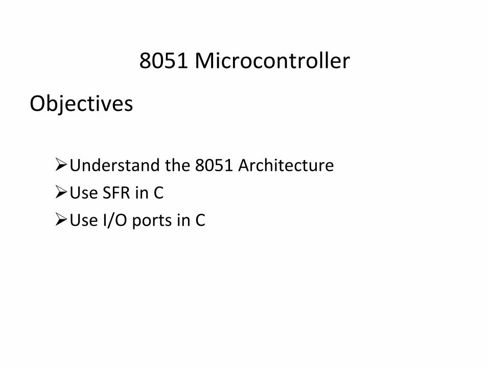
8051 Microcontroller Objectives Understand the 8051 Architecture Use SFR in C Use I/O ports in C
Transcript of 8051 Microcontroller Objectives - mmumullana.org · •The Intel 8051 is a very popular general...
8051 Microcontroller
Objectives
Understand the 8051 Architecture
Use SFR in C
Use I/O ports in C
3.1 Overview
• The Intel 8051 is a very popular general purpose microcontroller widely used for small scale embedded systems. Many vendors such as Atmel, Philips, and Texas Instruments produce MCS-51 family microcontroller chips.
• The 8051 is an 8-bit microcontroller with 8 bit data bus and 16-bit address bus. The 16 bit address bus can address a 64K( 216) byte code memory space and a separate 64K byte of data memory space. The 8051 has 4K on-chip read only code memory and 128 bytes of internal Random Access Memory (RAM)
Contd.
• Besides internal RAM, the 8051 has various Special Function Registers (SFR) such as the Accumulator, the B register, and many other control registers.
• 34 8-bit general purpose registers in total.
The ALU performs one 8-bit operation at a time.
• Two 16 bit /Counter timers
• 3 internal interrupts (one serial), 2 external interrupts.
• 4 8-bit I/O ports (3 of them are dual purposed). One of them used for serial port,
Some 8051 chips come with UART for serial communication and ADC for analog to digital conversion.
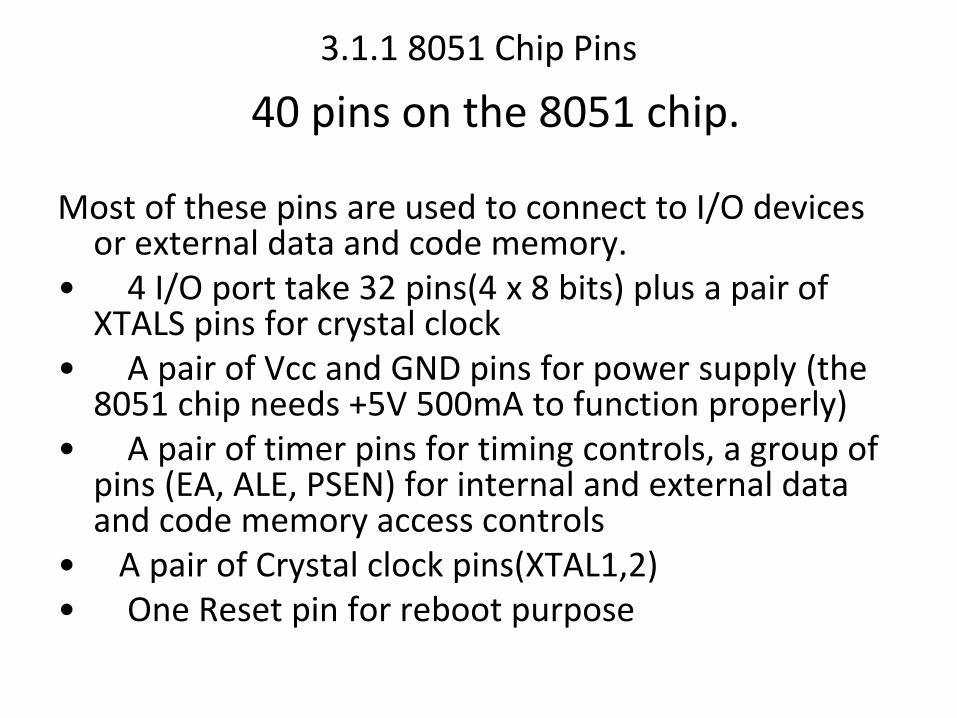
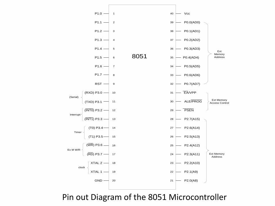
3.1.1 8051 Chip Pins
40 pins on the 8051 chip.
Most of these pins are used to connect to I/O devices or external data and code memory.
• 4 I/O port take 32 pins(4 x 8 bits) plus a pair of XTALS pins for crystal clock
• A pair of Vcc and GND pins for power supply (the 8051 chip needs +5V 500mA to function properly)
• A pair of timer pins for timing controls, a group of pins (EA, ALE, PSEN) for internal and external data and code memory access controls
• A pair of Crystal clock pins(XTAL1,2)• One Reset pin for reboot purpose
1
2
3
4
5
6
7
8
9
10
11
12
13
14
15
16
17
18
19
20
40
39
38
37
36
35
34
33
32
30
29
28
27
26
25
24
23
22
21
31
P1.0
P1.1
P1.2
P1.3
P1.4
P1.5
P1.6
RST
(RXD) P3.0
(TXD) P3.1
(INT0) P3.2
(INT1) P3.3
(T0) P3.4
(T1) P3.5
(WR) P3.6
XTAL 2
XTAL 1
GND
Vcc
P0.0(AD0)
P2.0(A8)
P2.1(A9)
P2.2(A10)
P2.3(A11)
P2.4(A12)
P2.5(A13)
P2.6(A14)
P2.7(A15)
PSEN
ALE/PROG
EA/VPP
P0.6(AD6)
P0.7(AD7)
P0.5(AD5)
P0.4(AD4)
P0.3(AD3)
P0.2(AD2)
P0.1(AD1)
(RD) P3.7
P1.7
(Serial)
interrupt
Timer
Ex M W/R
clock
Ext
Memory
Address
Ext Memory
Access Control
Ext Memory
Address
8051
Pin out Diagram of the 8051 Microcontroller
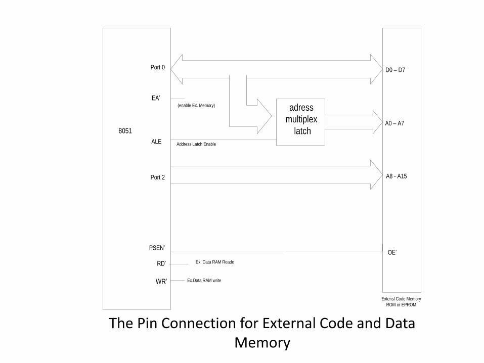
Port 0
(enable Ex. Memory)
Port 2
ALE Address Latch Enable
EA’
PSEN’
RD’
WR’ Ex.Data RAM write
OE’
A8 - A15
A0 – A7
D0 – D7
Ex. Data RAM Reade
Extensl Code Memory
ROM or EPROM
8051
adress
multiplex
latch
The Pin Connection for External Code and Data Memory
• The EA' (External Access) pin is used to control the internal or external memory access. The signal 0 is for external memory access and signal 1 for internal memory access.
• The PSEN' (Program Store Enable) is for reading external code memory when it is low (0) and EA is also 0.
• The ALE (Address Latch Enable) activates the port 0 joined with port 2 to provide 16 bit external address bus to access the external memory. The ALE multiplexes the P0: 1 for latching address on P0 as A0-A7 in the 16 bit address buss, 0 for latching P0 as data I/O.
• P0.x is named ADx because P0 is multiplexed for Address bus and Data bus at different clock time. WR' provides the signal to write external data memory RD' provides the signal to read external data and code memory.
3.1.2. System Clock and Oscillator Circuits
• The 8051 requires an external oscillator circuit. The oscillator circuit usually runs around 12MHz. the crystal generates 12M pulses in one second. The pulse is used to synchronize the system operation in a controlled pace..
• A machine cycle is minimum amount time a simplest machine instruction must take
• An 8051 machine cycle consists of 12 crystal pulses (ticks).
• instruction with a memory oprand needs multiple memory accesses(machine cycles).
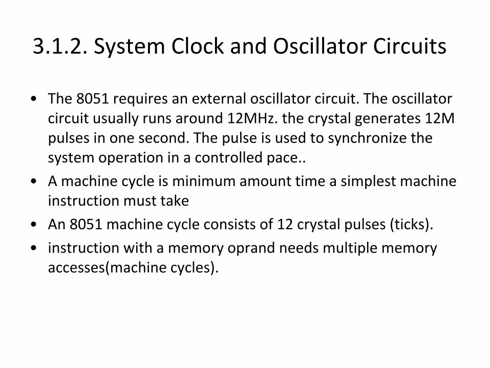
Contd.
The first 6 crystal pulses (clock cycle) is used to fetch the opcode and the second 6 pulses are used to perform the operation on the operands in the ALU. This gives an effective machine cycle rate at 1MIPS (Million Instructions Per Second).
XTAL!
XTAL2
GND
Crystal
Crystal to 8051 XTAL 1/2
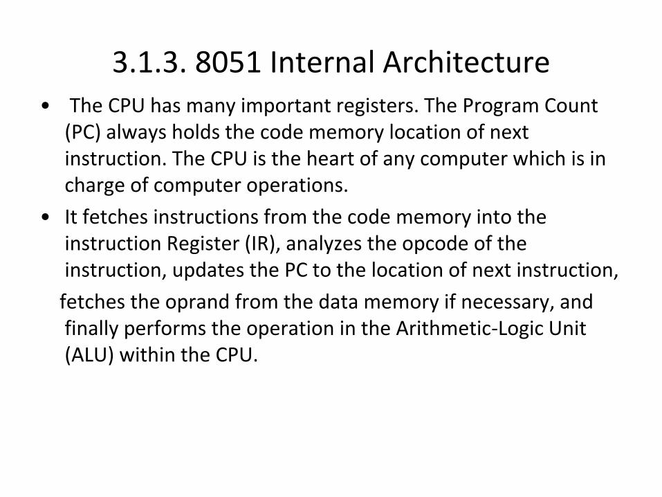
3.1.3. 8051 Internal Architecture • The CPU has many important registers. The Program Count
(PC) always holds the code memory location of next instruction. The CPU is the heart of any computer which is in charge of computer operations.
• It fetches instructions from the code memory into the instruction Register (IR), analyzes the opcode of the instruction, updates the PC to the location of next instruction,
fetches the oprand from the data memory if necessary, and finally performs the operation in the Arithmetic-Logic Unit (ALU) within the CPU.
Contd.
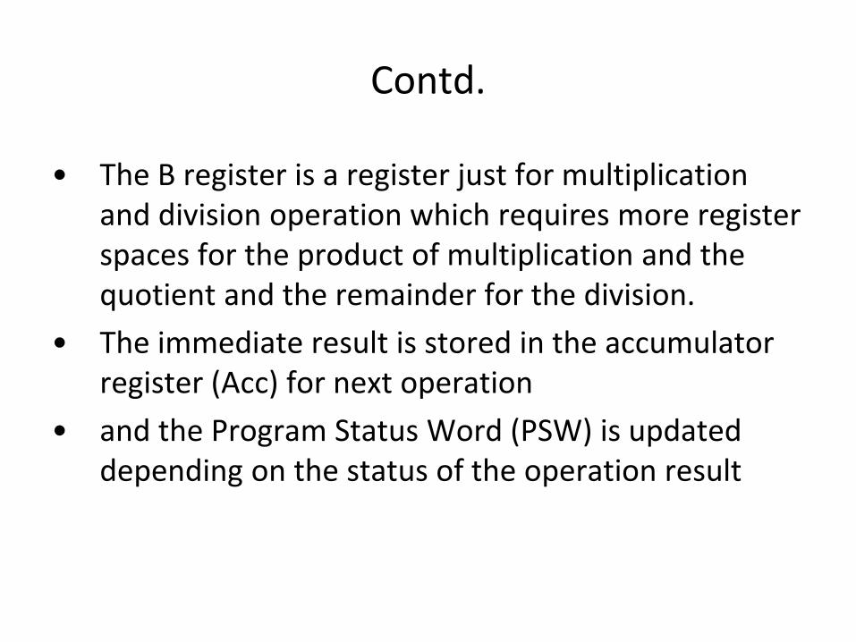
• The B register is a register just for multiplication and division operation which requires more register spaces for the product of multiplication and the quotient and the remainder for the division.
• The immediate result is stored in the accumulator register (Acc) for next operation
• and the Program Status Word (PSW) is updated depending on the status of the operation result
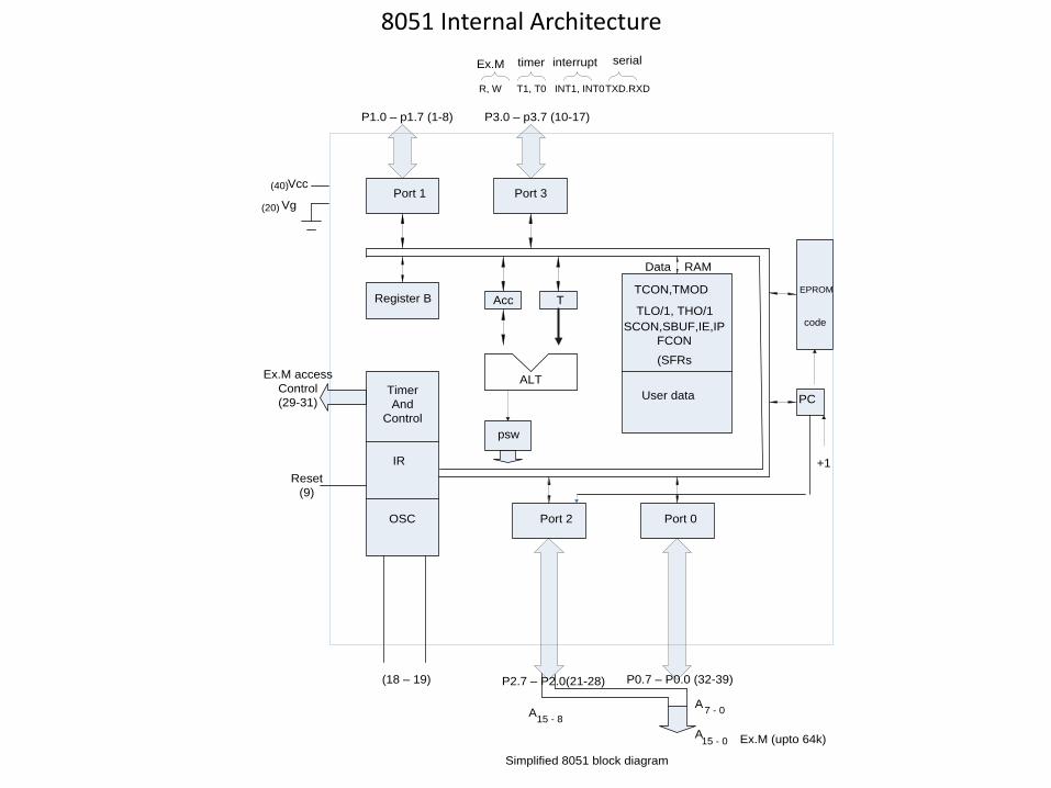
Port 1 Port 3
Port 2 Port 0
Register B Acc T
ALT
psw
Data RAM
TCON,TMOD
TLO/1, THO/1
SCON,SBUF,IE,IP
FCON
(SFRs
User data
EPROM
code
PCTimer
And
Control
IR
OSC
P1.0 – p1.7 (1-8) P3.0 – p3.7 (10-17)
Vcc(40)
Vg(20)
Ex.M access
Control
(29-31)
Reset
(9)
(18 – 19) P2.7 – P2.0(21-28)
A15 - 8
P0.7 – P0.0 (32-39)
A
A
7 - 0
15 - 0 Ex.M (upto 64k)
Simplified 8051 block diagram
Ex.M timer interrupt serial
R, W T1, T0 INT1, INT0TXD.RXD
+1
8051 Internal Architecture
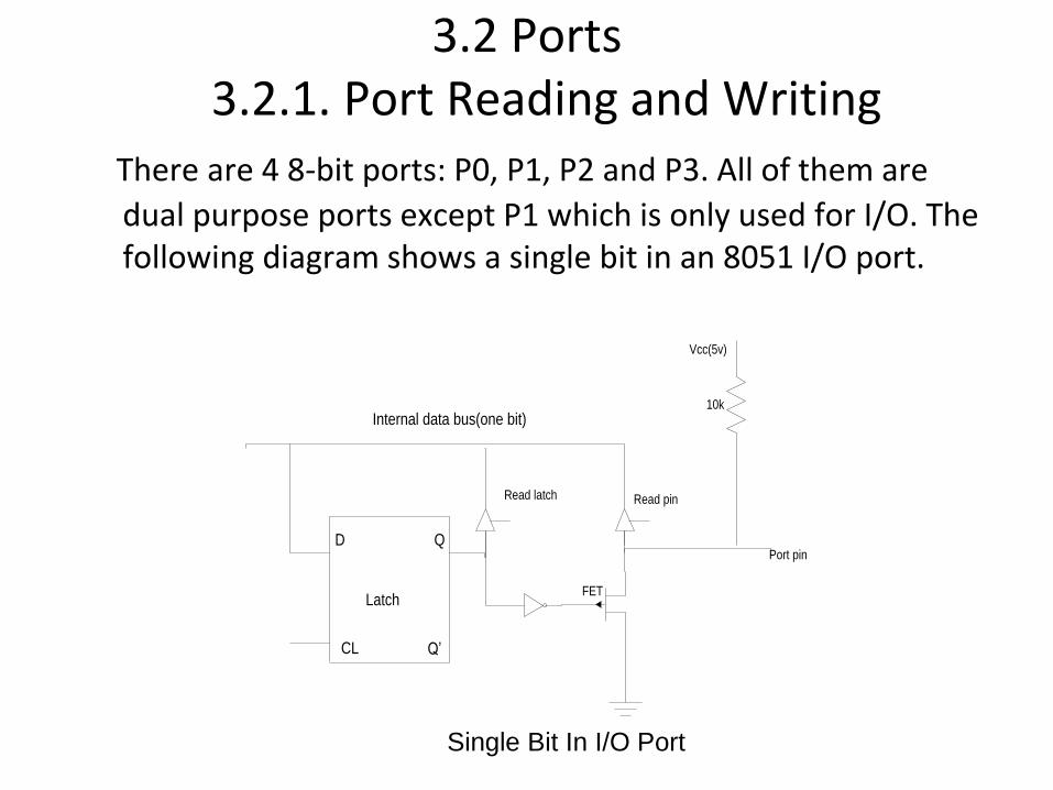
3.2 Ports3.2.1. Port Reading and Writing
There are 4 8-bit ports: P0, P1, P2 and P3. All of them are
dual purpose ports except P1 which is only used for I/O. The following diagram shows a single bit in an 8051 I/O port.
Internal data bus(one bit)
D Q
CL Q’
Latch
Read latch Read pin
Vcc(5v)
Port pin
10k
FET
Single Bit In I/O Port
Contd.
• When a C program writes a one byte value to a port or a single bit value to a bit of a port, just simply assign the value to the port as follows:
P1 = 0x12; or P1^2=1;• P1 represents the 8 bits of port 1 and P1^2 is the
pin #2 of the port 1 of 8051 defined in the reg51.h of C51, a C dedicated for 8051 family.
• When data is written to the port pin, it first appears on the latch input (D) and is then passed through to the output (Q) and through an inverter to the Field Effect Transistor (FET).
Contd.
• If you write a logic 0 to the port pin, this Q is logic 0 which is inverted to logic 1 and turns on the FET gate. It makes the port pin connected to ground (logic 0).
• If you write a logic 1 is written to the port pin, then Q is 1 which is inverted to a logic 0 and turns off the FET gate. Therefore the pin is at logic 1 because it is connected to high.
• You can see the written data is stored in the D latch after the data is written to the port pin.
Contd.
• However, you must initialize the port for reading before reading.
• If the latch was logic 0, then you will always get 0 regardless the data in the port pin because it is grounded through the FET gate.
• Therefore, in order to read the correct data from a port or a port pin, the last written logic (stored in the latch D) must be 0XFF(8 bits) or 1(single bit). E.g., you read entire P1 port or single bit of P1 port in this way:
unsigned char x; bit y;
P1 = 0xFF; //port reading initialization
x = P1; //read port
y = P1^2; //read bit
3.2.2. The Port Alternate Functions
• PORT P1 (Pins 1 to 8): The port P1 is a port dedicated for general I/O purpose. The other ports P0, P2 and P3 have dual roles in addition to their basic I/O function.
• PORT P0 (pins 32 to 39): When the external memory access is required then Port P0 is multiplexed for address bus and data bus that can be used to access external memory in conjunction with port P2. P0 acts as A0-A7 in address bus and D0-D7 for port data. It can be used for general purpose I/O if no external memory presents.
• PORT P2 (pins 21 to 28): Similar to P0, the port P2 can also play a role (A8-A15) in the address bus in conjunction with PORT P0 to access external memory.
Contd.
• PORT P3 (Pins 10 to 17):
In addition to acting as a normal I/O port, • P3.0 can be used for serial receive input pin(RXD) • P3.1 can be used for serial transmit output pin(TXD)
in a serial port, • P3.2 and P3.3 can be used as external interrupt
pins(INT0’ and INT1’), • P3.4 and P3.5 are used for external counter input
pins(T0 and T1), • P3.6 and P3.7 can be used as external data memory
write and read control signal pins(WR’ and RD’)read and write pins for memory access.
3.3 Memory and SFR3.3.1. Memory
• The 8051 code(program) memory is read-only, while the data memory is read/write accessible. The program memory( in EPROM) can be rewritten by the special programmer circuit.
• The 8051 memory is organized in a Harvard Architecture. Both the code memory space and data memory space begin at location 0x00 for internal or external memory which is different from the Princeton Architecture where code and data share same memory space.
• The advantage of the Harvard Architecture is not only doubling the memory capacity of the microcontroller with same number of address lines but also increases the reliability of the microcontroller, since there are no instructions to write to the code memory which is read only.
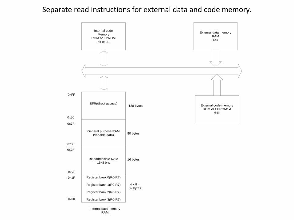
Separate read instructions for external data and code memory.
Internal code
Memory
ROM or EPROM
4k or up
SFR(direct access)
General purpose RAM
(variable data)
Bit addressible RAM
16x8 bits
Register bank 0(R0-R7)
Register bank 1(R0-R7)
Register bank 2(R0-R7)
Register bank 3(R0-R7)
External data memory
RAM
64k
External code memory
ROM or EPROMext
64k
Internal data memory
RAM
0xFF
0x80
0x7F
0x30
0x2F
0x20
0x1F
0x00
16 bytes
4 x 8 =
32 bytes
80 bytes
128 bytes
Contd.
• In this model, the data memory and code memory use separate maps by a special control line called Program Select Enable (PSEN’).
• This line (i.e. when PSEN’ = 0) is used to indicate that the 16 address lines are being used to address the code memory.
• When this line is ‘1’, the 16 address lines are being used to address the data memory.
Contd.
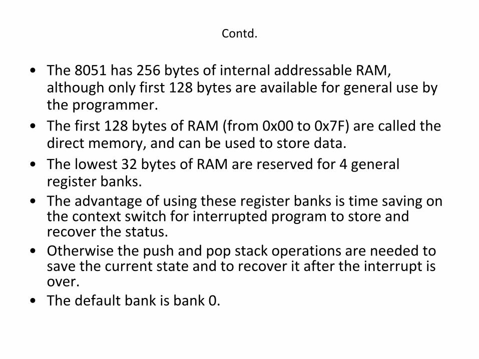
• The 8051 has 256 bytes of internal addressable RAM, although only first 128 bytes are available for general use by the programmer.
• The first 128 bytes of RAM (from 0x00 to 0x7F) are called the direct memory, and can be used to store data.
• The lowest 32 bytes of RAM are reserved for 4 general register banks.
• The advantage of using these register banks is time saving on the context switch for interrupted program to store and recover the status.
• Otherwise the push and pop stack operations are needed to save the current state and to recover it after the interrupt is over.
• The default bank is bank 0.
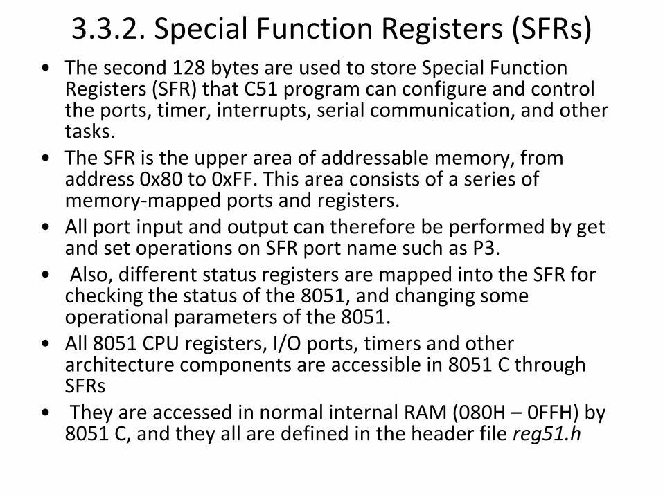
3.3.2. Special Function Registers (SFRs)• The second 128 bytes are used to store Special Function
Registers (SFR) that C51 program can configure and control the ports, timer, interrupts, serial communication, and other tasks.
• The SFR is the upper area of addressable memory, from address 0x80 to 0xFF. This area consists of a series of memory-mapped ports and registers.
• All port input and output can therefore be performed by get and set operations on SFR port name such as P3.
• Also, different status registers are mapped into the SFR for checking the status of the 8051, and changing some operational parameters of the 8051.
• All 8051 CPU registers, I/O ports, timers and other architecture components are accessible in 8051 C through SFRs
• They are accessed in normal internal RAM (080H – 0FFH) by 8051 C, and they all are defined in the header file reg51.h
Contd.
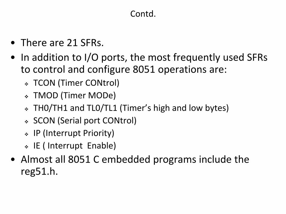
• There are 21 SFRs.
• In addition to I/O ports, the most frequently used SFRs to control and configure 8051 operations are: TCON (Timer CONtrol)
TMOD (Timer MODe)
TH0/TH1 and TL0/TL1 (Timer’s high and low bytes)
SCON (Serial port CONtrol)
IP (Interrupt Priority)
IE ( Interrupt Enable)
• Almost all 8051 C embedded programs include the reg51.h.
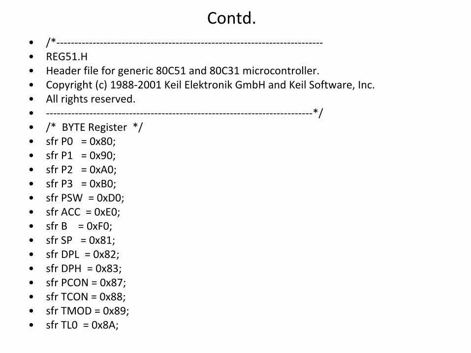
Contd.• /*--------------------------------------------------------------------------• REG51.H• Header file for generic 80C51 and 80C31 microcontroller.• Copyright (c) 1988-2001 Keil Elektronik GmbH and Keil Software, Inc.• All rights reserved.• --------------------------------------------------------------------------*/• /* BYTE Register */• sfr P0 = 0x80;• sfr P1 = 0x90;• sfr P2 = 0xA0;• sfr P3 = 0xB0;• sfr PSW = 0xD0;• sfr ACC = 0xE0;• sfr B = 0xF0;• sfr SP = 0x81;• sfr DPL = 0x82;• sfr DPH = 0x83;• sfr PCON = 0x87;• sfr TCON = 0x88;• sfr TMOD = 0x89;• sfr TL0 = 0x8A;
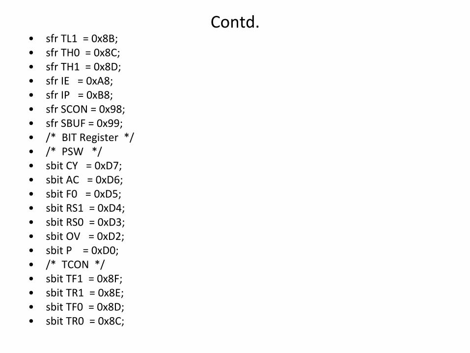
Contd.• sfr TL1 = 0x8B;• sfr TH0 = 0x8C;• sfr TH1 = 0x8D;• sfr IE = 0xA8;• sfr IP = 0xB8;• sfr SCON = 0x98;• sfr SBUF = 0x99;• /* BIT Register */• /* PSW */• sbit CY = 0xD7;• sbit AC = 0xD6;• sbit F0 = 0xD5;• sbit RS1 = 0xD4;• sbit RS0 = 0xD3;• sbit OV = 0xD2;• sbit P = 0xD0;• /* TCON */• sbit TF1 = 0x8F;• sbit TR1 = 0x8E; • sbit TF0 = 0x8D;• sbit TR0 = 0x8C;
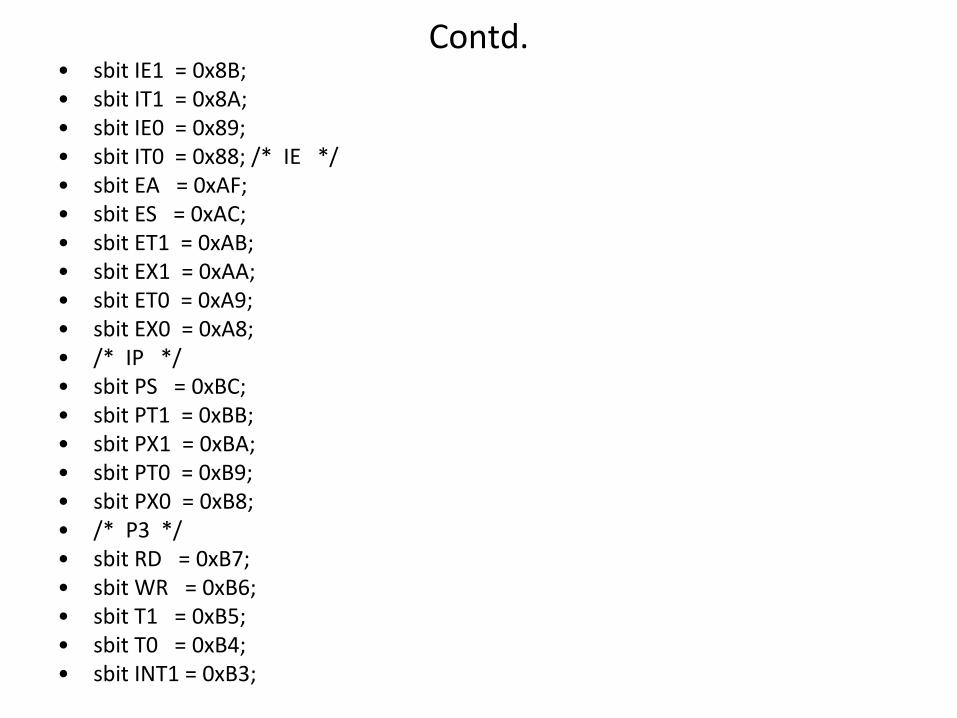
Contd.• sbit IE1 = 0x8B;• sbit IT1 = 0x8A;• sbit IE0 = 0x89;• sbit IT0 = 0x88; /* IE */• sbit EA = 0xAF;• sbit ES = 0xAC;• sbit ET1 = 0xAB;• sbit EX1 = 0xAA;• sbit ET0 = 0xA9;• sbit EX0 = 0xA8;• /* IP */ • sbit PS = 0xBC;• sbit PT1 = 0xBB;• sbit PX1 = 0xBA;• sbit PT0 = 0xB9;• sbit PX0 = 0xB8;• /* P3 */• sbit RD = 0xB7;• sbit WR = 0xB6;• sbit T1 = 0xB5; • sbit T0 = 0xB4;• sbit INT1 = 0xB3;
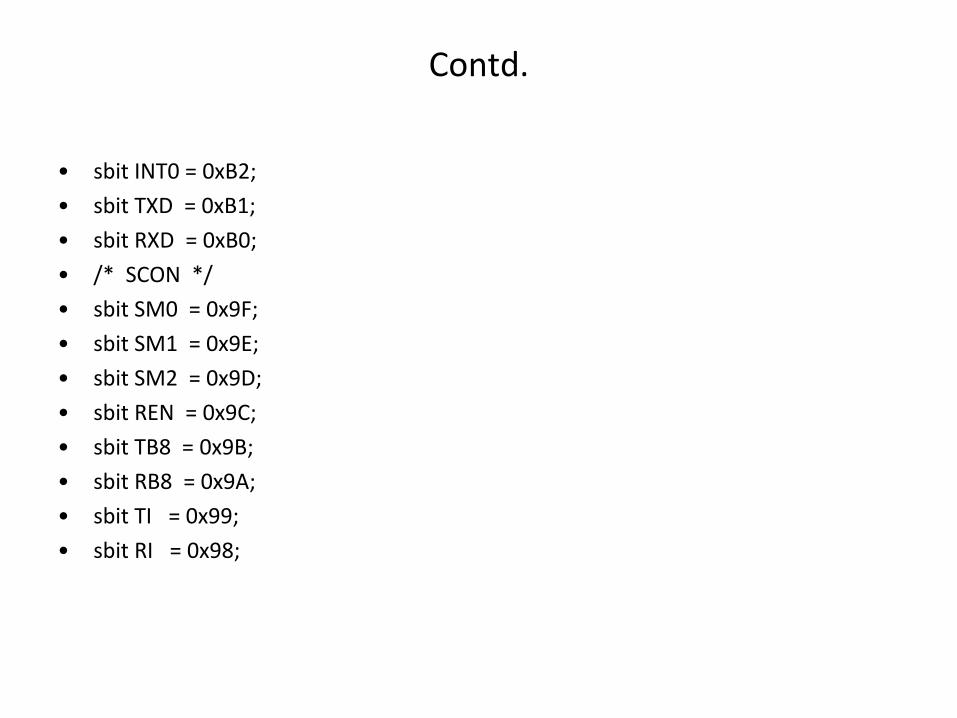
Contd.
• sbit INT0 = 0xB2;
• sbit TXD = 0xB1;
• sbit RXD = 0xB0;
• /* SCON */
• sbit SM0 = 0x9F;
• sbit SM1 = 0x9E;
• sbit SM2 = 0x9D;
• sbit REN = 0x9C;
• sbit TB8 = 0x9B;
• sbit RB8 = 0x9A;
• sbit TI = 0x99;
• sbit RI = 0x98;
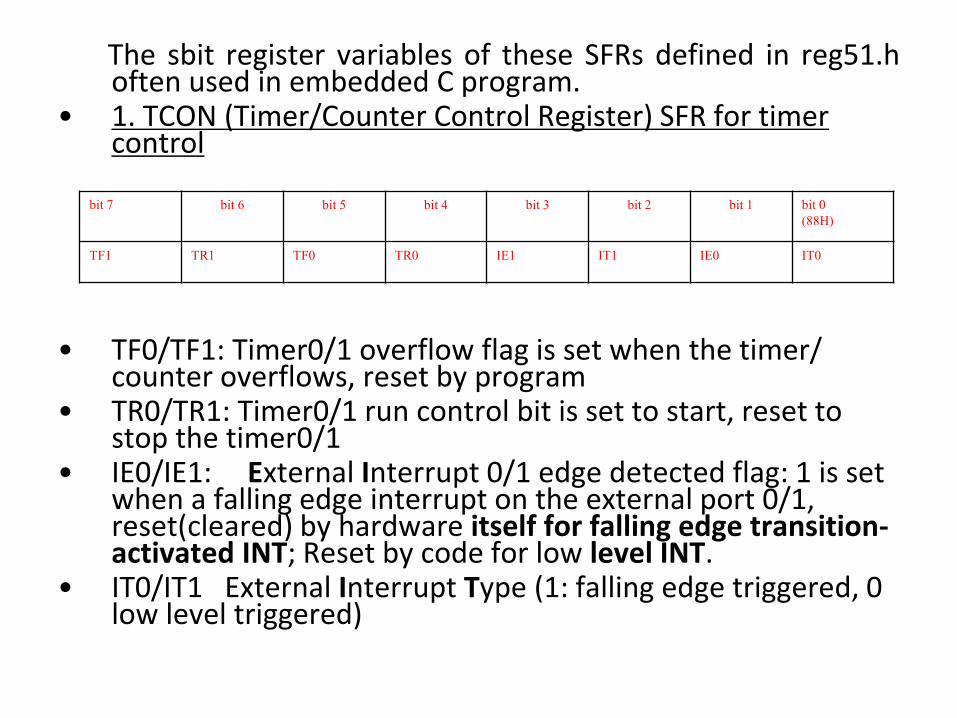
The sbit register variables of these SFRs defined in reg51.hoften used in embedded C program.
• 1. TCON (Timer/Counter Control Register) SFR for timer control
• TF0/TF1: Timer0/1 overflow flag is set when the timer/ counter overflows, reset by program
• TR0/TR1: Timer0/1 run control bit is set to start, reset to stop the timer0/1
• IE0/IE1: External Interrupt 0/1 edge detected flag: 1 is set when a falling edge interrupt on the external port 0/1, reset(cleared) by hardware itself for falling edge transition-activated INT; Reset by code for low level INT.
• IT0/IT1 External Interrupt Type (1: falling edge triggered, 0 low level triggered)
bit 7 bit 6 bit 5 bit 4 bit 3 bit 2 bit 1 bit 0
(88H)
TF1 TR1 TF0 TR0 IE1 IT1 IE0 IT0
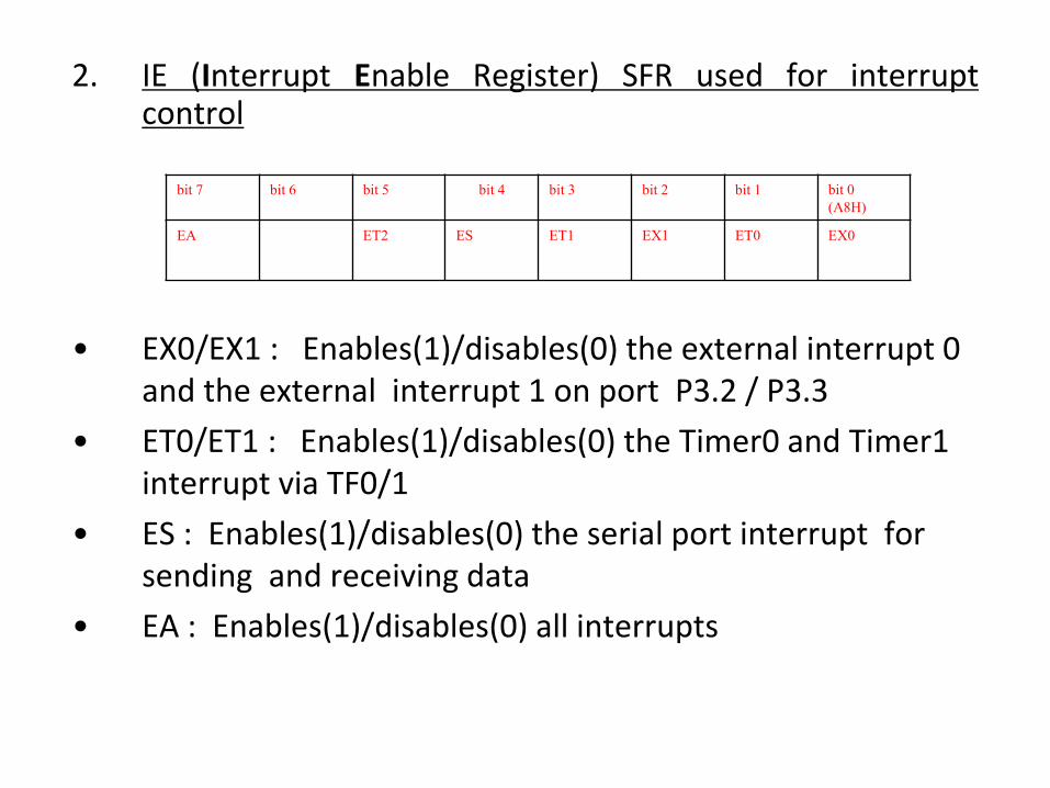
2. IE (Interrupt Enable Register) SFR used for interruptcontrol
• EX0/EX1 : Enables(1)/disables(0) the external interrupt 0 and the external interrupt 1 on port P3.2 / P3.3
• ET0/ET1 : Enables(1)/disables(0) the Timer0 and Timer1 interrupt via TF0/1
• ES : Enables(1)/disables(0) the serial port interrupt for sending and receiving data
• EA : Enables(1)/disables(0) all interrupts
bit 7 bit 6 bit 5 bit 4 bit 3 bit 2 bit 1 bit 0
(A8H)
EA ET2 ES ET1 EX1 ET0 EX0
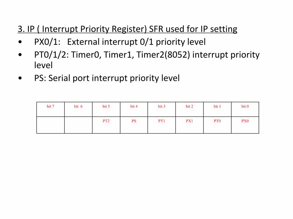
3. IP ( Interrupt Priority Register) SFR used for IP setting
• PX0/1: External interrupt 0/1 priority level
• PT0/1/2: Timer0, Timer1, Timer2(8052) interrupt priority level
• PS: Serial port interrupt priority level
bit 7 bit 6 bit 5 bit 4 bit 3 bit 2 bit 1 bit 0
PT2 PS PT1 PX1 PT0 PX0
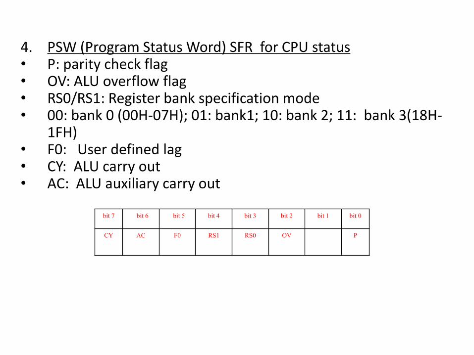
4. PSW (Program Status Word) SFR for CPU status• P: parity check flag• OV: ALU overflow flag• RS0/RS1: Register bank specification mode • 00: bank 0 (00H-07H); 01: bank1; 10: bank 2; 11: bank 3(18H-
1FH)• F0: User defined lag• CY: ALU carry out• AC: ALU auxiliary carry out
bit 7 bit 6 bit 5 bit 4 bit 3 bit 2 bit 1 bit 0
CY AC F0 RS1 RS0 OV P
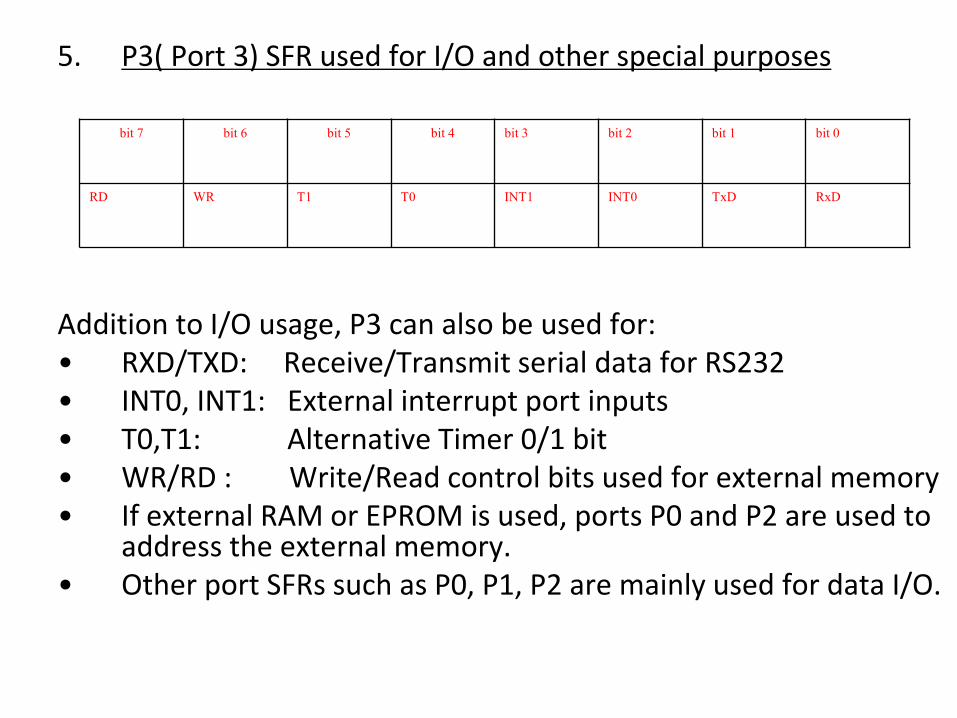
5. P3( Port 3) SFR used for I/O and other special purposes
Addition to I/O usage, P3 can also be used for:• RXD/TXD: Receive/Transmit serial data for RS232• INT0, INT1: External interrupt port inputs• T0,T1: Alternative Timer 0/1 bit• WR/RD : Write/Read control bits used for external memory• If external RAM or EPROM is used, ports P0 and P2 are used to
address the external memory.• Other port SFRs such as P0, P1, P2 are mainly used for data I/O.
bit 7 bit 6 bit 5 bit 4 bit 3 bit 2 bit 1 bit 0
RD WR T1 T0 INT1 INT0 TxD RxD
6. TL0/TL1 SFRs: Lower byte of Timer 0/1, used to set timer interrupt period
TH0/TH1 SFRs: Higher byte of Timer 0,used to set timer interrupt period
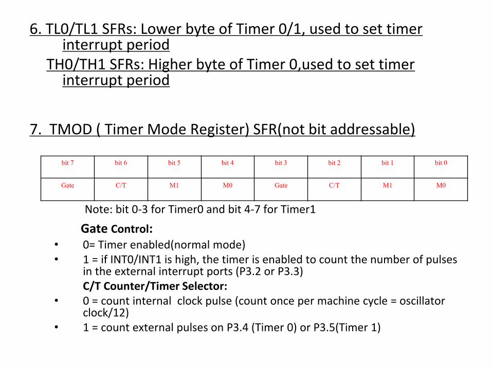
7. TMOD ( Timer Mode Register) SFR(not bit addressable)
Note: bit 0-3 for Timer0 and bit 4-7 for Timer1
Gate Control:• 0= Timer enabled(normal mode)• 1 = if INT0/INT1 is high, the timer is enabled to count the number of pulses
in the external interrupt ports (P3.2 or P3.3)C/T Counter/Timer Selector:
• 0 = count internal clock pulse (count once per machine cycle = oscillator clock/12)
• 1 = count external pulses on P3.4 (Timer 0) or P3.5(Timer 1)
bit 7 bit 6 bit 5 bit 4 bit 3 bit 2 bit 1 bit 0
Gate C/T M1 M0 Gate C/T M1 M0
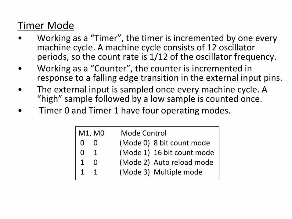
Timer Mode• Working as a “Timer”, the timer is incremented by one every
machine cycle. A machine cycle consists of 12 oscillator periods, so the count rate is 1/12 of the oscillator frequency.
• Working as a “Counter”, the counter is incremented in response to a falling edge transition in the external input pins.
• The external input is sampled once every machine cycle. A “high” sample followed by a low sample is counted once.
• Timer 0 and Timer 1 have four operating modes.
M1, M0 Mode Control0 0 (Mode 0) 8 bit count mode0 1 (Mode 1) 16 bit count mode1 0 (Mode 2) Auto reload mode1 1 (Mode 3) Multiple mode
Contd.
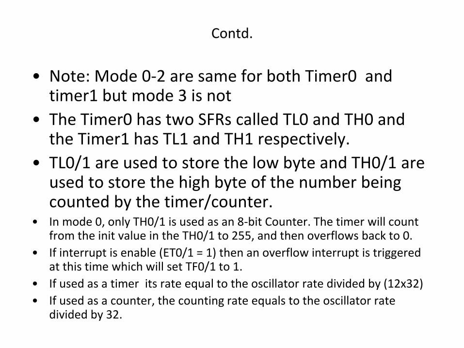
• Note: Mode 0-2 are same for both Timer0 and timer1 but mode 3 is not
• The Timer0 has two SFRs called TL0 and TH0 and the Timer1 has TL1 and TH1 respectively.
• TL0/1 are used to store the low byte and TH0/1 are used to store the high byte of the number being counted by the timer/counter.
• In mode 0, only TH0/1 is used as an 8-bit Counter. The timer will count from the init value in the TH0/1 to 255, and then overflows back to 0.
• If interrupt is enable (ET0/1 = 1) then an overflow interrupt is triggered at this time which will set TF0/1 to 1.
• If used as a timer its rate equal to the oscillator rate divided by (12x32)
• If used as a counter, the counting rate equals to the oscillator rate divided by 32.
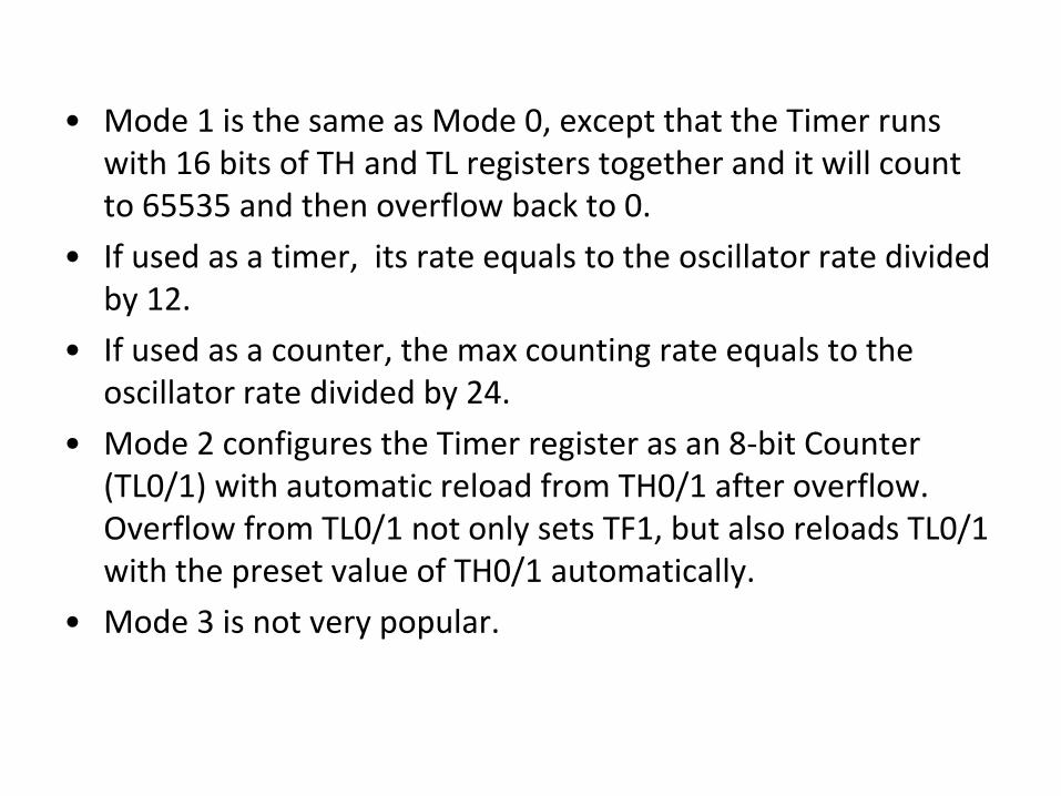
• Mode 1 is the same as Mode 0, except that the Timer runs with 16 bits of TH and TL registers together and it will count to 65535 and then overflow back to 0.
• If used as a timer, its rate equals to the oscillator rate divided by 12.
• If used as a counter, the max counting rate equals to the oscillator rate divided by 24.
• Mode 2 configures the Timer register as an 8-bit Counter (TL0/1) with automatic reload from TH0/1 after overflow. Overflow from TL0/1 not only sets TF1, but also reloads TL0/1 with the preset value of TH0/1 automatically.
• Mode 3 is not very popular.
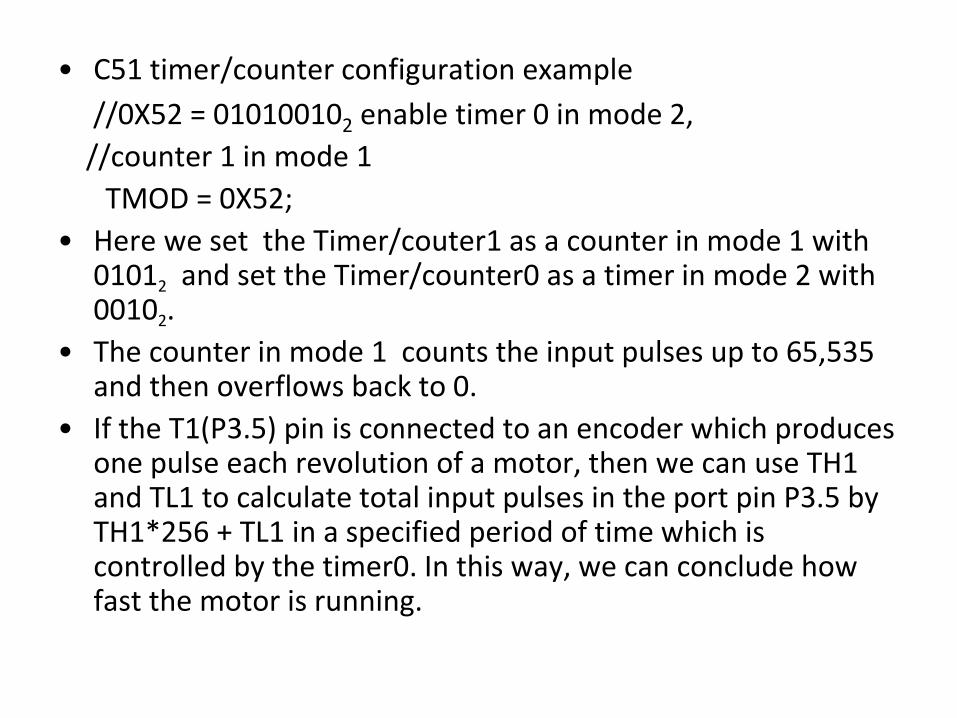
• C51 timer/counter configuration example
//0X52 = 010100102 enable timer 0 in mode 2,
//counter 1 in mode 1
TMOD = 0X52;
• Here we set the Timer/couter1 as a counter in mode 1 with 01012 and set the Timer/counter0 as a timer in mode 2 with 00102.
• The counter in mode 1 counts the input pulses up to 65,535 and then overflows back to 0.
• If the T1(P3.5) pin is connected to an encoder which produces one pulse each revolution of a motor, then we can use TH1 and TL1 to calculate total input pulses in the port pin P3.5 by TH1*256 + TL1 in a specified period of time which is controlled by the timer0. In this way, we can conclude how fast the motor is running.
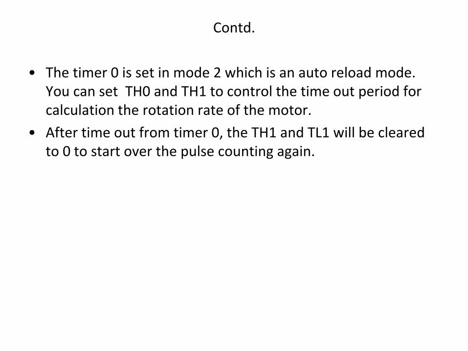
Contd.
• The timer 0 is set in mode 2 which is an auto reload mode. You can set TH0 and TH1 to control the time out period for calculation the rotation rate of the motor.
• After time out from timer 0, the TH1 and TL1 will be cleared to 0 to start over the pulse counting again.
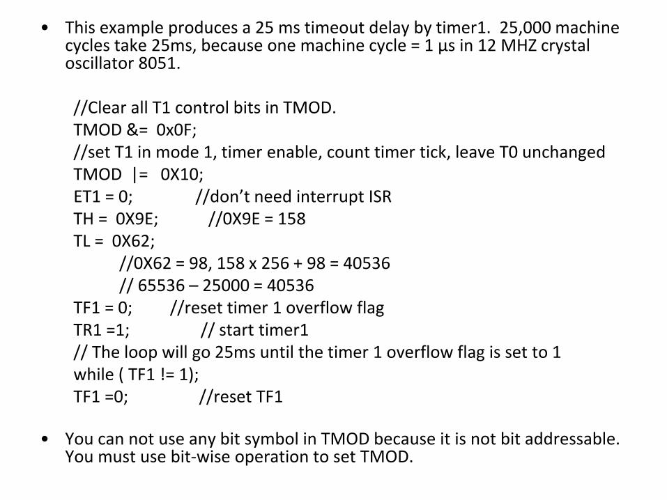
• This example produces a 25 ms timeout delay by timer1. 25,000 machine cycles take 25ms, because one machine cycle = 1 µs in 12 MHZ crystal oscillator 8051.
//Clear all T1 control bits in TMOD.TMOD &= 0x0F; //set T1 in mode 1, timer enable, count timer tick, leave T0 unchangedTMOD |= 0X10; ET1 = 0; //don’t need interrupt ISRTH = 0X9E; //0X9E = 158TL = 0X62;
//0X62 = 98, 158 x 256 + 98 = 40536// 65536 – 25000 = 40536
TF1 = 0; //reset timer 1 overflow flagTR1 =1; // start timer1// The loop will go 25ms until the timer 1 overflow flag is set to 1while ( TF1 != 1); TF1 =0; //reset TF1
• You can not use any bit symbol in TMOD because it is not bit addressable. You must use bit-wise operation to set TMOD.
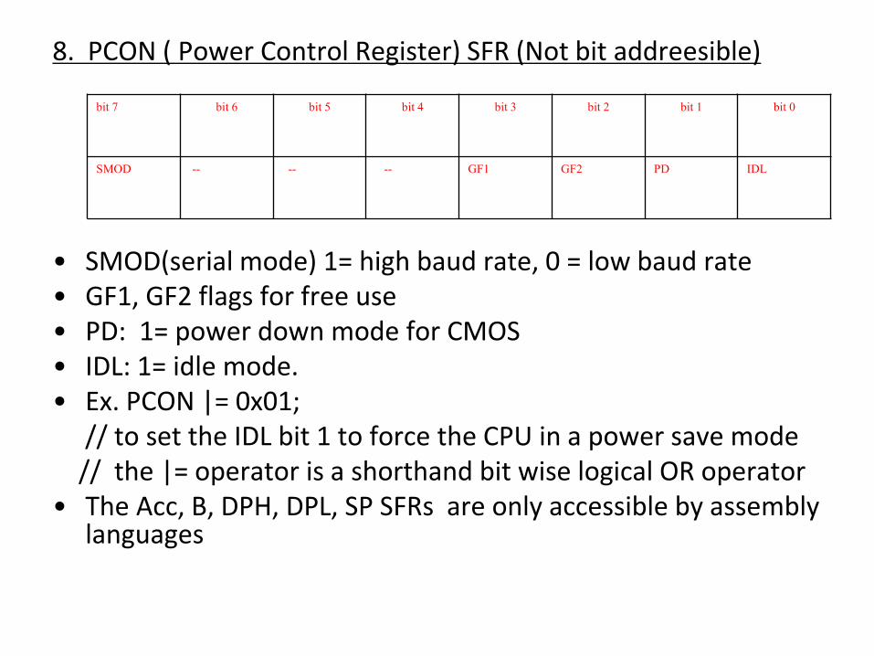
8. PCON ( Power Control Register) SFR (Not bit addreesible)
• SMOD(serial mode) 1= high baud rate, 0 = low baud rate• GF1, GF2 flags for free use• PD: 1= power down mode for CMOS • IDL: 1= idle mode. • Ex. PCON |= 0x01;
// to set the IDL bit 1 to force the CPU in a power save mode // the |= operator is a shorthand bit wise logical OR operator
• The Acc, B, DPH, DPL, SP SFRs are only accessible by assembly languages
bit 7 bit 6 bit 5 bit 4 bit 3 bit 2 bit 1 bit 0
SMOD -- -- -- GF1 GF2 PD IDL
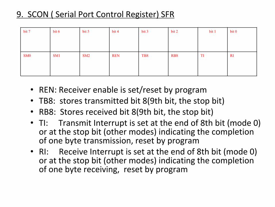
9. SCON ( Serial Port Control Register) SFR
• REN: Receiver enable is set/reset by program• TB8: stores transmitted bit 8(9th bit, the stop bit)• RB8: Stores received bit 8(9th bit, the stop bit)• TI: Transmit Interrupt is set at the end of 8th bit (mode 0)
or at the stop bit (other modes) indicating the completion of one byte transmission, reset by program
• RI: Receive Interrupt is set at the end of 8th bit (mode 0) or at the stop bit (other modes) indicating the completion of one byte receiving, reset by program
bit 7 bit 6 bit 5 bit 4 bit 3 bit 2 bit 1 bit 0
SM0 SM1 SM2 REN TB8 RB8 TI RI
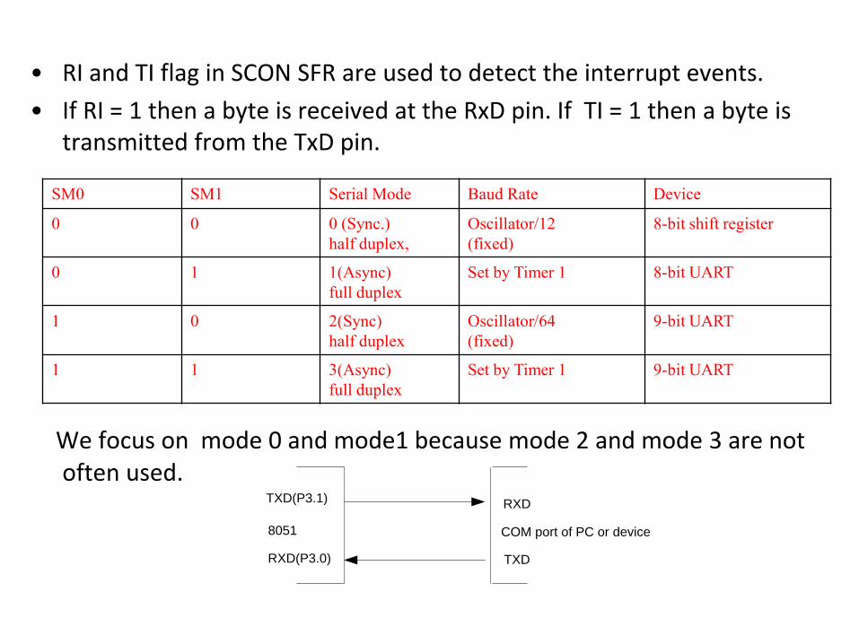
• RI and TI flag in SCON SFR are used to detect the interrupt events.
• If RI = 1 then a byte is received at the RxD pin. If TI = 1 then a byte is transmitted from the TxD pin.
We focus on mode 0 and mode1 because mode 2 and mode 3 are not often used.
SM0 SM1 Serial Mode Baud Rate Device
0 0 0 (Sync.)
half duplex,
Oscillator/12
(fixed)
8-bit shift register
0 1 1(Async)
full duplex
Set by Timer 1 8-bit UART
1 0 2(Sync)
half duplex
Oscillator/64
(fixed)
9-bit UART
1 1 3(Async)
full duplex
Set by Timer 1 9-bit UART
TXD(P3.1)
RXD(P3.0)
RXD
TXD
COM port of PC or device8051
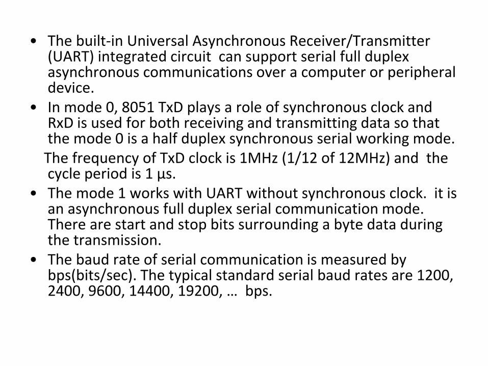
• The built-in Universal Asynchronous Receiver/Transmitter (UART) integrated circuit can support serial full duplex asynchronous communications over a computer or peripheral device.
• In mode 0, 8051 TxD plays a role of synchronous clock and RxD is used for both receiving and transmitting data so that the mode 0 is a half duplex synchronous serial working mode.
The frequency of TxD clock is 1MHz (1/12 of 12MHz) and the cycle period is 1 µs.
• The mode 1 works with UART without synchronous clock. it is an asynchronous full duplex serial communication mode. There are start and stop bits surrounding a byte data during the transmission.
• The baud rate of serial communication is measured by bps(bits/sec). The typical standard serial baud rates are 1200, 2400, 9600, 14400, 19200, … bps.
XTALOscillator
11.0592 MHz÷12
Machine cycle freq.
921.6 kHz
÷32by UART
28800 Hzfor timer default baud rate
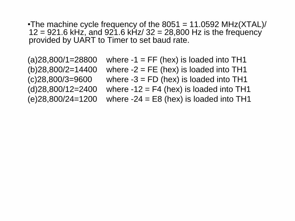
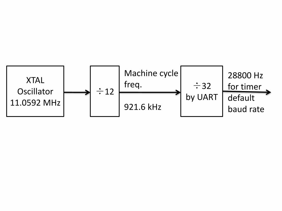
•The machine cycle frequency of the 8051 = 11.0592 MHz(XTAL)/ 12 = 921.6 kHz, and 921.6 kHz/ 32 = 28,800 Hz is the frequency provided by UART to Timer to set baud rate.
(a)28,800/1=28800 where -1 = FF (hex) is loaded into TH1
(b)28,800/2=14400 where -2 = FE (hex) is loaded into TH1
(c)28,800/3=9600 where -3 = FD (hex) is loaded into TH1
(d)28,800/12=2400 where -12 = F4 (hex) is loaded into TH1
(e)28,800/24=1200 where -24 = E8 (hex) is loaded into TH1
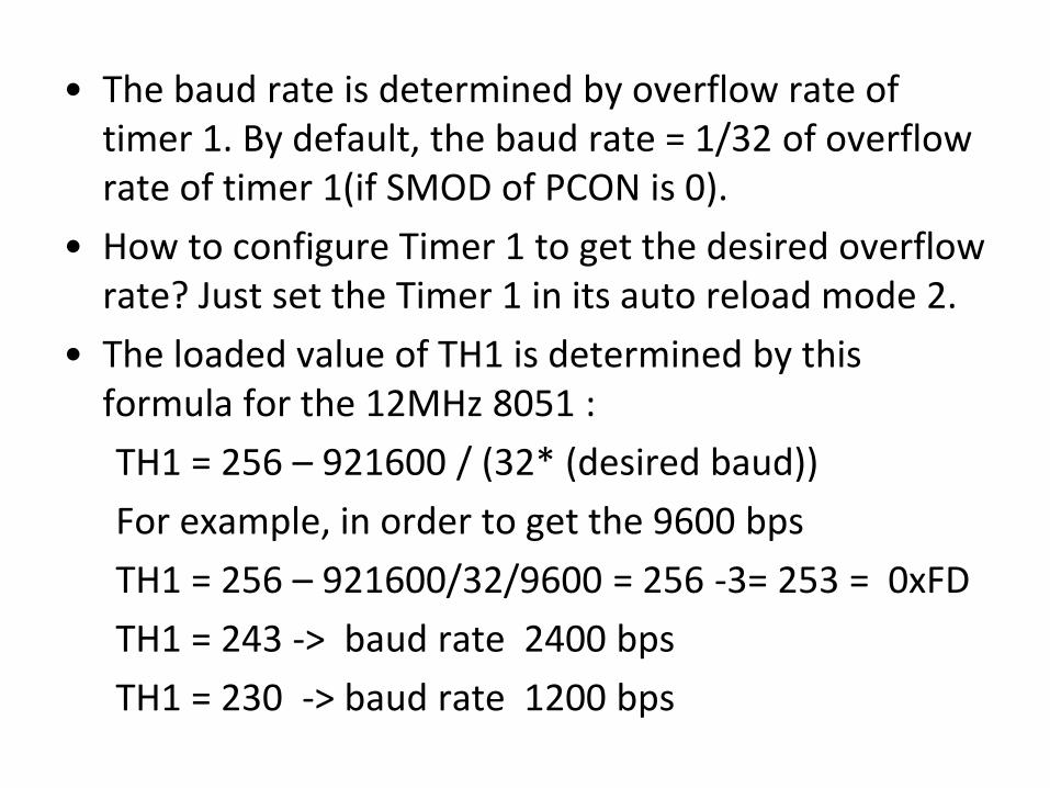
• The baud rate is determined by overflow rate of timer 1. By default, the baud rate = 1/32 of overflow rate of timer 1(if SMOD of PCON is 0).
• How to configure Timer 1 to get the desired overflow rate? Just set the Timer 1 in its auto reload mode 2.
• The loaded value of TH1 is determined by this formula for the 12MHz 8051 :
TH1 = 256 – 921600 / (32* (desired baud))
For example, in order to get the 9600 bps
TH1 = 256 – 921600/32/9600 = 256 -3= 253 = 0xFD
TH1 = 243 -> baud rate 2400 bps
TH1 = 230 -> baud rate 1200 bps
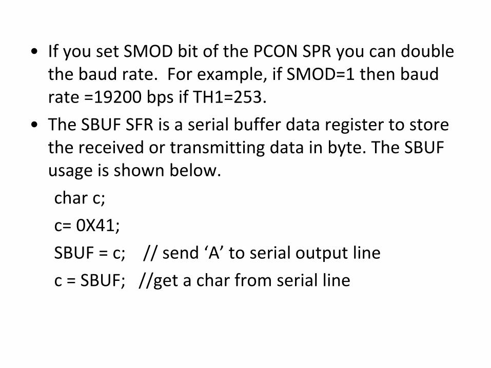
• If you set SMOD bit of the PCON SPR you can double the baud rate. For example, if SMOD=1 then baud rate =19200 bps if TH1=253.
• The SBUF SFR is a serial buffer data register to store the received or transmitting data in byte. The SBUF usage is shown below.
char c;
c= 0X41;
SBUF = c; // send ‘A’ to serial output line
c = SBUF; //get a char from serial line
3.4 SFRs and Interrupts
• Interrupt is an internal or external event that suspends a program and transfers the control to an event handler or ISR to handle the event.
• After the service is over, the control is back to the suspended program to resume the execution. The microcontroller in a embedded system connects many devices and needs to handle service requests from devices all the time.
You can classify Registers for function
1. IE enables interrupts
EX0/EX1: Enable external interrupt INT0/INT1
ET0/ET1: Enable Timer 0/Timer1 interrupt
ES: Enable serial interrupt
EA: Enable global interrupt
Set 1 in a bit to enable its interrupt, e.g. EA =1;
reset 0 to masks that interrupt, e.g., EA = 0;
2. Interrupt Flags
The interrupt flags are set to 1 when the interrupts occur, the flag 0 indicates no interrupt.
IE0/IE1 in TCON - For External Interrupts
TF0/TF1 in TCON - For Timer Interrupts
TI/RI in SCON - For Serial Interrupts
3. Interrupt Priority
There are two types of interrupt priority: User Defined Priority and Automatic Priority
*User Defined Priority
The IP register is used to define priority levels by users. The high priority interrupt can preempt the low priority interrupt. There are only two levels of interrupt priority.
//The external interrupt INT0 at port P3.2 is assigned a high priority.
EX0 = 1; //the external interrupt INT1 at port P3.3 is assigned a low priority.
EX1 = 0;
*Automatic Priority
In each priority level, a priority is given in order of:
INT0, TF0, INT1, TF1, SI.
For example, if two external interrupts are set at same priority level, then INT0 has precedence over INT1.

1) External Interrupts• An external interrupt is triggered by a low level or negative
edge on INT0 and INT1 which depends on the external interrupt type setting.
Set up an external interrupt type by IT0 and IT1 of TCON SFR.
• E.g.,
IT0 = 1; //set INT0 as Negative edge triggered
IT1 = 0; // set INT1 as Level Triggered
• The external interrupt source may be a sensor, ADC, or a switch connected to port P3.2(INT0) or P3.3(INT1). You use IE0/IE1 to test the external interrupt events: Ex. If IE0 = 1 then the INT0 interrupt takes place.
• Note that if an external interrupt is set to low level trigger, the interrupt will reoccur as long as P3.2 or P3.3 is low that makes the code difficult to manage.
• You enable external interrupt by EX0/EX1 of IE SFR. E.g., EA = 1;EX0 = 1; //enable external interrupt INT0
• If the interrupt is level activated, then IE0/1 flag has to be cleared by user software asEX1 = 0;
• You don’t need to reset the edge triggered external interrupt.
• This fragment makes the INT1 external interrupt ready on port P3.3 pin:EA =1;EX1 =1;IT1 =1;
2) Timer/Counter Interrupts
• This unit can be used as a counter to count external pulses on P3.4 and P3.5 pins or it can be used to count the pulses produced by the crystal oscillator of the microcontroller.
• Timer Interrupt is caused by Timer 0/ Timer1 overflow.TF0/1: //1 => Condition occurred
//Enabled using IE
ET0/1 = 1, EA = 1
• E.g.TMOD = 0X12; //set timer 1 in mode 1, timer 0 in mode 2.
EA=1; // enable global interrupt
TH1=0; // Make timer 1 overflow every 240 clocks
TL1=16; // (240=256-16 240 µs)
ET0=1; // enable timer 0
TR0=1; //start timer0
// Timer 0 overflows after 65535 clocks.
ET1=1; // enable timer 1
TR1=1; //start timer 1
3)Serial Interrupts
• Serial communication with Universal Asynchronous Receive Transmit (UART) protocol transmits or receives the bits of a byte one after the other in a timed sequence on a single wire.
• It is used to communicate any serial port of devices and computers.
• The serial interrupt is caused by completion of a serial byte transmitting or receiving.
• The transmit data pin (TxD) is at P3.1 and the receive data pin (RxD) is at P3.0.
• All communication modes are controlled through SCON, a non bit addressable SFR. The SCON bits are defined as SM0, SM1, SM2, REN, TB8, RB8, TI, RI.
• You use timers to control the baud of asynchronous serial communication which is set by TMOD and TCON as we discussed before
• Example of full duplex asynchronous serial communication in mode 1 to transmit and receive data simultaneously#include <reg51.h>main()
{char c;
// set timer1 in auto reload 8 bit timer mode 2TMOD=0x20;
// load timer 1 to generate baud rate of 9600 bps
TH1 = 0xFD;TL1 = 0XFD;
// set serial communication in mode 1SCON=0x40;
// start timer 1
TR1 = 1;
While(1){
// enable reception
REN = 1;
//wait until data is receivedwhile((SCON & 0X02) == 0);
// same as while(RI==0);
// reset receive flag
RI=0;
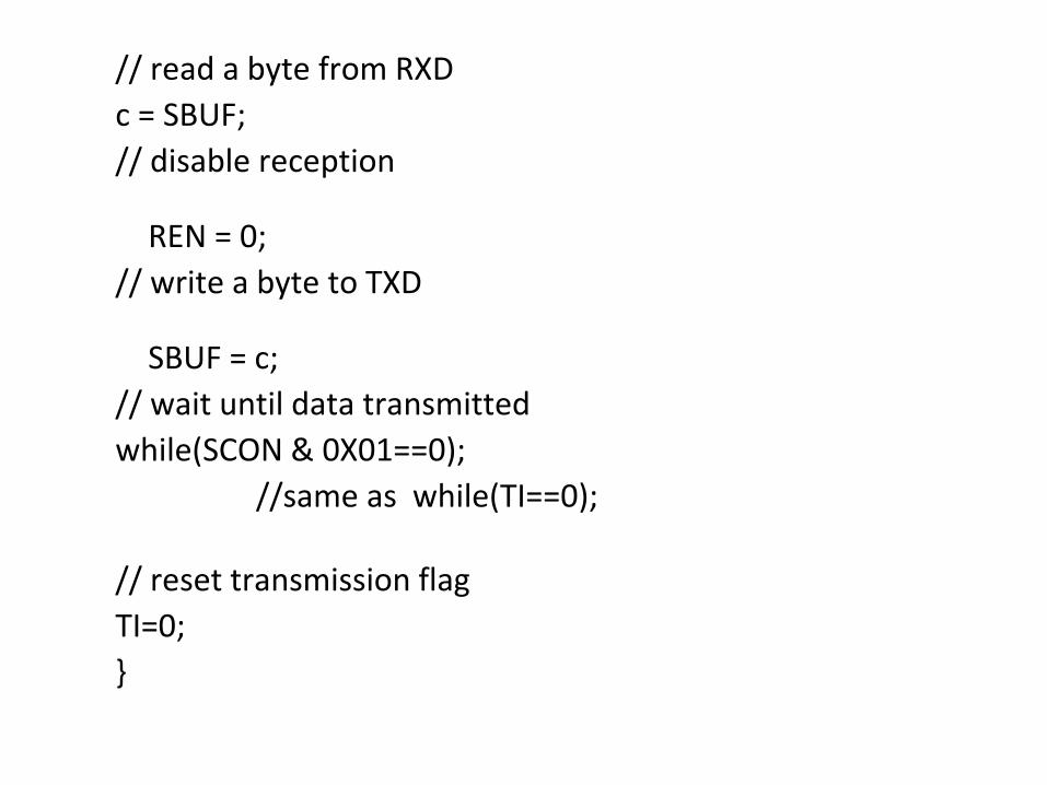
// read a byte from RXD
c = SBUF;
// disable reception
REN = 0;
// write a byte to TXD
SBUF = c;
// wait until data transmitted
while(SCON & 0X01==0);
//same as while(TI==0);
// reset transmission flag
TI=0;
}
Summary
• This chapter explores the internal architecture of 8051 microcontroller and its interface. The Harvard architecture for separation of code and data memory is discussed. The detail and usage of 8051 SFRs, especially, the timer control SFRs such as TMOD, TCON and serial control SFR such as SCON, the interrupt control registers such as IE. The configurations of external interrupt, timer/counter interrupt and serial communication interrupt with C51
• Understand how to use 8051 to connect and control external devices such as sensor, switch, LED, LCD, keypad.
• Learn how to design and handle the timing clock issue in the embedded systems.
• This chapter is a foundation for the next chapter on the embedded programming in C.