Datasheet IR2302 & (PbF) - Infineon Technologies
22
HALF-BRIDGE DRIVER Features • Floating channel designed for bootstrap operation Fully operational to +600V Tolerant to negative transient voltage dV/dt immune • Gate drive supply range from 5 to 20V • Undervoltage lockout for both channels • 3.3V, 5V and 15V input logic compatible • Cross-conduction prevention logic • Matched propagation delay for both channels • High side output in phase with IN input • Logic and power ground +/- 5V offset. • Internal 540ns dead-time • Lower di/dt gate driver for better noise immunity • Shut down input turns off both channels • 8-Lead SOIC also available LEAD-FREE (PbF). IR2302 ( S ) & (PbF) Data Sheet No. PD60207 Rev.A www.irf.com 1 Packages µ µ 2106/2301//2108//2109/2302/2304 Feature Comparison Description The IR2302(S) are high voltage, high speed power MOSFET and IGBT drivers with depen- dent high and low side referenced output channels. Proprietary HVIC and latch immune CMOS technologies enable ruggedized monolithic construction. The logic input is compatible with standard CMOS or LSTTL output, down to 3.3V logic. The output drivers feature a high pulse current buffer stage designed for minimum driver cross-conduction. The floating channel can be used to drive an N-channel power MOSFET or IGBT in the high side configuration which operates up to 600 volts. 8-Lead PDIP IR2302 8-Lead SOIC IR2302(S) (Also available LEAD-FREE (PbF)) Typical Connection IR2302 (Refer to Lead Assignments for correct configuration). This/ These diagram(s) show elec- trical connections only. Please refer to our Application Notes and DesignTips for proper circuit board layout.
Transcript of Datasheet IR2302 & (PbF) - Infineon Technologies

HALF-BRIDGE DRIVER
Features• Floating channel designed for bootstrap operation
Fully operational to +600VTolerant to negative transient voltagedV/dt immune
• Gate drive supply range from 5 to 20V
• Undervoltage lockout for both channels
• 3.3V, 5V and 15V input logic compatible
• Cross-conduction prevention logic
• Matched propagation delay for both channels
• High side output in phase with IN input
• Logic and power ground +/- 5V offset.
• Internal 540ns dead-time
• Lower di/dt gate driver for better noiseimmunity
• Shut down input turns off both channels
• 8-Lead SOIC also available LEAD-FREE (PbF).
IR2302(S) & (PbF)
Data Sheet No. PD60207 Rev.A
www.irf.com 1
Packages
!
"#$%$
&''!
* 7" !
*"#$%$ 9
:;7"<7µ &''!
= 7" !
="$' 9
:;7"<7µ &''!
2106/2301//2108//2109/2302/2304 Feature Comparison
" #$%$ 9 !
DescriptionThe IR2302(S) are high voltage, high speedpower MOSFET and IGBT drivers with depen-dent high and low side referenced outputchannels. Proprietary HVIC and latch immune CMOS technologies enable ruggedized monolithic construction.The logic input is compatible with standard CMOS or LSTTL output, down to 3.3V logic. The output driversfeature a high pulse current buffer stage designed for minimum driver cross-conduction. The floating channel canbe used to drive an N-channel power MOSFET or IGBT in the high side configuration which operates up to600 volts.
8-Lead PDIP
IR2302
8-Lead SOIC
IR2302(S)
(Also available LEAD-FREE (PbF))
Typical Connection
IR2302
&
&>
&'
#
%!
$
''
$
&
%?
&
(Refer to Lead Assignments for
correct configuration). This/
These diagram(s) show elec-
trical connections only. Please refer to our Application Notes
and DesignTips for proper circuit board layout.

IR2302(S) & (PbF)
2 www.irf.com
Recommended Operating ConditionsThe input/output logic timing diagram is shown in figure 1. For proper operation the device should be used within the
recommended conditions. The VS offset rating is tested with all supplies biased at 15V differential.
Note 1: Logic operational for VS of -5 to +600V. Logic state held for VS of -5V to -VBS. (Please refer to the Design Tip
DT97-3 for more details).
VB High side floating supply absolute voltage VS + 5 VS + 20
VS High side floating supply offset voltage Note 1 600
VHO High side floating output voltage VS VB
VCC Low side and logic fixed supply voltage 5 20
VLO Low side output voltage 0 VCC
VIN Logic input voltage (IN & SD) COM VCC
TA Ambient temperature -40 150 °C
Symbol Definition Min. Max. Units
V
Symbol Definition Min. Max. Units
VB High side floating absolute voltage -0.3 625
VS High side floating supply offset voltage VB - 25 VB + 0.3
VHO High side floating output voltage VS - 0.3 VB + 0.3
VCC Low side and logic fixed supply voltage -0.3 25
VLO Low side output voltage -0.3 VCC + 0.3
VIN Logic input voltage (IN & SD) COM - 0.3 VCC + 0.3
dVS/dt Allowable offset supply voltage transient — 50 V/ns
PD Package power dissipation @ TA ≤ +25°C (8 Lead PDIP) — 1.0
(8 Lead SOIC) — 0.625
RthJA Thermal resistance, junction to ambient (8 Lead PDIP) — 125
(8 Lead SOIC) — 200
TJ Junction temperature — 150
TS Storage temperature -50 150
TL Lead temperature (soldering, 10 seconds) — 300
Absolute Maximum RatingsAbsolute maximum ratings indicate sustained limits beyond which damage to the device may occur. All voltage param-
eters are absolute voltages referenced to COM. The thermal resistance and power dissipation ratings are measured
under board mounted and still air conditions.
V
°C/W
W
°C
IR2302(S) & (PbF)
www.irf.com 3
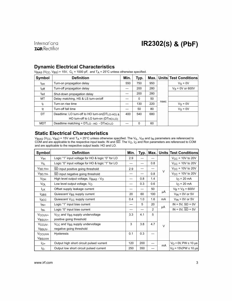
Dynamic Electrical CharacteristicsVBIAS (VCC, VBS) = 15V, CL = 1000 pF, and TA = 25°C unless otherwise specified.
Symbol Definition Min. Typ. Max. Units Test Conditions
ton Turn-on propagation delay 550 750 950 VS = 0V
toff Turn-off propagation delay — 200 280 VS = 0V or 600V
tsd Shut-down propagation delay — 200 280
MT Delay matching, HS & LS turn-on/off — 0 50
tr Turn-on rise time — 130 220 VS = 0V
tf Turn-off fall time — 50 80 VS = 0V
DT Deadtime: LO turn-off to HO turn-on(DTLO-HO) & 400 540 680
HO turn-off to LO turn-on (DTHO-LO)
MDT Deadtime matching = DTLO - HO - DTHO-LO — 0 60
nsec
Static Electrical CharacteristicsVBIAS (VCC, VBS) = 15V and TA = 25°C unless otherwise specified. The VIL, VIH and IIN parameters are referenced to
COM and are applicable to the respective input leads: IN and SD. The VO, IO and Ron parameters are referenced to COM
and are applicable to the respective output leads: HO and LO.
Symbol Definition Min. Typ. Max. Units Test Conditions
VIH Logic “1” input voltage for HO & logic “0” for LO 2.9 — — VCC = 10V to 20V
VIL Logic “0” input voltage for HO & logic “1” for LO — — 0.8 VCC = 10V to 20V
VSD,TH+ SD input positive going threshold 2.9 — — VCC = 10V to 20V
VSD,TH- SD input negative going threshold — — 0.8 VCC = 10V to 20V
VOH High level output voltage, VBIAS - VO — 0.8 1.4 IO = 20 mA
VOL Low level output voltage, VO — 0.3 0.6 IO = 20 mA
ILK Offset supply leakage current — — 50 VB = VS = 600V
IQBS Quiescent VBS supply current 20 60 100 VIN = 0V or 5V
IQCC Quiescent VCC supply current 0.4 1.0 1.6 mA VIN = 0V or 5V
IIN+ Logic “1” input bias current — 5 20 IN = 5V, SD = 0V
IIN- Logic “0” input bias current — — 2 IN = 0V, SD = 5V
VCCUV+ VCC and VBS supply undervoltage 3.3 4.1 5
VBSUV+ positive going threshold
VCCUV- VCC and VBS supply undervoltage 3 3.8 4.7
VBSUV- negative going threshold
VCCUVH Hysteresis 0.1 0.3 —
VBSUVH
IO+ Output high short circuit pulsed vurrent 120 200 — VO = 0V, PW ≤ 10 µs
IO- Output low short circuit pulsed current 250 350 — VO = 15V,PW ≤ 10 µs
V
µA
µA
V
mA

IR2302(S) & (PbF)
4 www.irf.com
Functional Block Diagrams
SD
UVDETECT
DELAY COM
LO
VCC
IN VS
HO
VB
PULSEFILTER
HVLEVEL
SHIFTER
R
R
S
Q
UVDETECT
PULSEGENERATOR
VSS/COMLEVELSHIFT
VSS/COMLEVELSHIFT
+5V
DEADTIME

IR2302(S) & (PbF)
www.irf.com 5
Lead Assignments
8 Lead PDIP 8 Lead SOIC
(Also available LEAD-FREE (PbF)
1
2
3
4
8
7
6
5
VCC
IN
SD
COM
VB
HO
VS
LO
1
2
3
4
8
7
6
5
VCC
IN
SD
COM
VB
HO
VS
LO
IR2302 IR2302S
Lead DefinitionsSymbol Description
IN Logic input for high and low side gate driver outputs (HO and LO), in phase with HO
SD Logic input for shutdown
VB High side floating supply
HO High side gate drive output
VS High side floating supply return
VCC Low side and logic fixed supply
LO Low side gate drive output
COM Low side return

IR2302(S) & (PbF)
6 www.irf.com
Figure 4. Deadtime Waveform Definitions
$
#
7] 7]
=]
]
% =]
]
%#
%#
!^ #%
#%
Figure 3. Shutdown Waveform Definitions
'
#
%
7]
=]
Figure 1. Input/Output Timing Diagram
'
$
#
%
Figure 2. Switching Time Waveform Definitions
$_#`
qqq
%
#
7] 7]
=] =]
] ]
$_%`

IR2302(S) & (PbF)
www.irf.com 7
300
500
700
900
1100
1300
-50 -25 0 25 50 75 100 125
Temperature (oC)
Turn
-on
Prop
agat
ion
Del
ay (n
s)
Typ.
M ax.
Figure 6A. Turn-on Propagation Delay vs. Temperature
M in.
300
500
700
900
1100
1300
1500
5 10 15 20
Supply Voltage (V)
Turn
-on
Prop
agat
ion
Del
ay (n
s)
Figure 6B. Turn-on Propagation Delay vs. Supply Voltage
Typ.
M ax.
M in.
Figure 5. Delay Matching Waveform Definitions
#
7] 7]
]
%
=]
!
#%
!
$_%`
$ _#`

IR2302(S) & (PbF)
8 www.irf.com
300
500
700
900
1100
1300
3 6 9 12 15
Input Voltage (V)
Turn
-on
Prop
agat
ion
Del
ay (n
s)
Figure 6C. Turn-on Propagation Delay vs. Input Voltage
Typ.
M ax.
M in.
0
100
200
300
400
500
-50 -25 0 25 50 75 100 125
Temperature (oC)
Turn
-off
Prop
agat
ion
Del
ay (n
s)
Typ.
M ax.
Figure 7A. Turn-off Propagation Delay vs. Temperature
100
150
200
250
300
350
400
3 6 9 12 15Input Voltage (V)
Turn
-off
Prop
agat
ion
Del
ay (n
s)
Figure 7C. Turn-off Propagation Delay vs. Input Voltage
Typ.
M ax.
100
200
300
400
500
600
700
5 10 15 20
Supply Voltage (V)
Turn
-off
Prop
agat
ion
Del
ay (n
s)
Figure 7B. Turn-off Propagation Delay vs. Supply Voltage
Typ.
M ax.
IR2302(S) & (PbF)
www.irf.com 9
100
200
300
400
500
600
700
5 10 15 20
Supply Voltage (V)
Shut
-dow
n Pr
opag
atio
n D
elay
(ns)
Typ.
M ax.
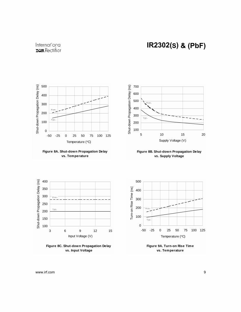
Figure 8B. Shut-down Propagation Delay vs. Supply Voltage
0
100
200
300
400
500
-50 -25 0 25 50 75 100 125
Temperature (oC)
Shut
-dow
n Pr
opag
atio
n D
elay
(ns)
Typ.
M ax.
Figure 8A. Shut-down Propagation Delay vs. Temperature
100
150
200
250
300
350
400
3 6 9 12 15Input Voltage (V)
Shut
-dow
n Pr
opag
atio
n D
elay
(ns)
Figure 8C. Shut-down Propagation Delay vs. Input Voltage
Typ.
M ax.
0
100
200
300
400
500
-50 -25 0 25 50 75 100 125
Temperature (oC)
Turn
-on
Ris
e Ti
me
(ns)
Typ.
M ax.
Figure 9A. Turn-on Rise Time vs. Temperature
IR2302(S) & (PbF)
10 www.irf.com
0
100
200
300
400
500
600
700
5 10 15 20Supply Voltage (V)
Turn
-on
Ris
e Ti
me
(ns)
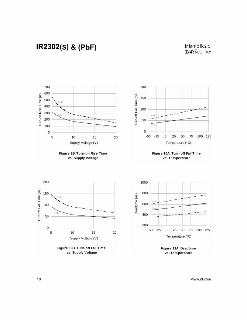
Figure 9B. Turn-on Rise Time vs. Supply Voltage
Typ.
M ax.
0
50
100
150
200
-50 -25 0 25 50 75 100 125
Temperature (oC)
Turn
-off
Fall
Tim
e (n
s)
Typ.
M ax.
Figure 10A. Turn-off Fall Time vs. Temperature
0
50
100
150
200
5 10 15 20
Supply Voltage (V)
Turn
-off
Fall
Tim
e (n
s)
Figure 10B. Turn-off Fall Time vs. Supply Voltage
Typ.
M ax.
200
400
600
800
1000
-50 -25 0 25 50 75 100 125
Temperature (oC)
Dea
dtim
e (n
s)
Figure 11A. Deadtime vs. Temperature
M in.
M ax.
Typ.

IR2302(S) & (PbF)
www.irf.com 11
0
200
400
600
800
1000
5 10 15 20Supply Voltage (V)
Dea
dtim
e (n
s)
Figure 11B. Deadtime vs. Supply Voltage
Typ.
M ax.
M in.
0
1
2
3
4
5
6
7
0 50 100 150 200
RDT (KΩ)
Dea
dtim
e (s
)
Figure 11C. Deadtime vs. RDT
Typ.
M ax.
M in.
0
1
2
3
4
5
6
-50 -25 0 25 50 75 100 125
Temperature (oC)
Logi
c "1
" Inp
ut V
olta
ge (V
)
M ax.
Figure 12A. Logic "1" Input Voltage vs. Temperature
0
1
2
3
4
5
6
5 10 15 20Supply Voltage (V)
Logi
c "1
" Inp
ut V
olta
ge (V
)
Figure 12B. Logic "1" Input Voltage vs. Supply Voltage
M ax.

IR2302(S) & (PbF)
12 www.irf.com
0
1
2
3
4
5
6
-50 -25 0 25 50 75 100 125
Temperature (oC)
Logi
c "0
" Inp
ut V
olta
ge (V
)
M in.
Figure 13A. Logic "0" Input Voltage vs. Temperature
0
1
2
3
4
5
6
-50 -25 0 25 50 75 100 125
Temperature (oC)
SD In
put P
ositi
ve G
oing
Thr
esho
ld (V
M ax.
Figure 14A. SD Input Positive Going Thresholdvs. Temperature
0
1
2
3
4
5
6
5 10 15 20Supply Voltage (V)
SD In
put P
ositi
ve G
oing
Thr
esho
ld (V
Figure 14B. SD Input Positive Going Thresholdvs. Supply Voltage
M ax.
0
1
2
3
4
5
6
5 10 15 20Supply Voltage (V)
Logi
c "0
" Inp
ut V
olta
ge (V
)
Figure 13B. Logic "0" Input Voltage vs. Supply Voltage
M in.

IR2302(S) & (PbF)
www.irf.com 13
0
1
2
3
4
5
6
-50 -25 0 25 50 75 100 125
Temperature (oC)
SD In
put N
egat
ive
Goi
ng T
hres
hold
(V)
M in.
Figure 15A. SD Input Negative Going Thresholdvs. Temperature
0
1
2
3
4
5
6
5 10 15 20Supply Voltage (V)
SD In
put N
egat
ive
Goi
ng T
hres
hold
(V
Figure 15B. SD Input Negative Going Thresholdvs. Supply Voltage
M in.
0
1
2
3
4
-50 -25 0 25 50 75 100 125
Temperature (oC)
Hig
h Le
vel O
utpu
t Vol
tage
(V)
M ax.
Figure 16A. High Level Output Voltage vs. Temperature
Typ.
0
1
2
3
4
5
6
5 10 15 20Supply Voltage (V)
Hig
h Le
vel O
utpu
t Vol
tage
(V)
Figure 16B. High Level Output Voltage vs. Supply Voltage
Typ.
M ax.

IR2302(S) & (PbF)
14 www.irf.com
0.0
0.5
1.0
1.5
2.0
-50 -25 0 25 50 75 100 125
Temperature (oC)
Low
Lev
el O
utpu
t Vol
tage
(V)
M ax.
Figure 17A. Low Level Output Voltage vs. Temperature
Typ.0.0
0.5
1.0
1.5
2.0
5 10 15 20
Supply Voltage (V)
Low
Lev
el O
utpu
t Vol
tage
(V)
Figure 17B. Low Level Output Voltage vs. Supply Voltage
Typ.
M ax.
0
100
200
300
400
500
-50 -25 0 25 50 75 100 125
Temperature (oC)
Offs
et S
uppl
y Le
akag
e C
urre
nt (
A)
M ax.
Figure 18A. Offset Supply Leakage Current vs. Temperature
0
100
200
300
400
500
100 200 300 400 500 600Offset Supply Voltage (V)
Offs
et S
uppl
y Le
akag
e C
urre
nt (m
A)
Figure 18B. Offset Supply Leakage Current vs. Offset Supply Voltage
M ax.

IR2302(S) & (PbF)
www.irf.com 15
0
50
100
150
200
-50 -25 0 25 50 75 100 125
Temperature (oC)
Qui
esce
nt V
BS S
uppl
y C
urre
nt (
A)
M in.
Figure 19A. Quiescent VBS Supply Current vs. Temperature
Typ.
M ax.
0
50
100
150
200
5 10 15 20VBS Supply Voltage (V)
Qui
esce
nt V
BS S
uppl
y C
urre
nt (
A)
Figure 19B. Quiescent VBS Supply Current vs. VBS Supply Voltage
Typ.
M ax.
M in.
0.0
0.5
1.0
1.5
2.0
2.5
3.0
-50 -25 0 25 50 75 100 125
Temperature (oC)
Qui
esce
nt V
CC S
uppl
y C
urre
nt (m
A)
M in.
Figure 20A. Quiescent VCC Supply Currentvs. Temperature
Typ.
M ax
0
0.5
1
1.5
2
2.5
3
5 10 15 20VCC Supply Voltage (V)
Qui
esce
nt V
CC S
uppl
y C
urre
nt (m
A)
Figure 20B. Quiescent VCC Supply Currentvs. VCC Supply Voltage
Typ.M ax.
M in.

IR2302(S) & (PbF)
16 www.irf.com
0
10
20
30
40
50
60
-50 -25 0 25 50 75 100 125
Temperature (oC)
Logi
c "1
" Inp
ut B
ias
Cur
rent
(A)
Figure 21A. Logic "1" Input Bias Current vs. Temperature
Typ.
M ax.
0
10
20
30
40
50
5 10 15 20Supply Voltage (V)
Logi
c "1
" Inp
ut B
ias
Cur
rent
(mA)
Figure 21B. Logic "1" Input Bias Current vs. Supply Voltage
Typ.
M ax.
0
1
2
3
4
5
-50 -25 0 25 50 75 100 125
Temperature (oC)
Logi
c "0
" Inp
ut B
ias
Cur
rent
(A)
Figure 22A. Logic "0" Input Bias Current vs. Temperature
M ax.
0
1
2
3
4
5
5 10 15 20Supply Voltage (V)
Logi
c "0
" Inp
ut B
ias
Cur
rent
(mA)
Figure 22B. Logic "0" Input Bias Current vs. Supply Voltage
M ax.

IR2302(S) & (PbF)
www.irf.com 17
2
3
4
5
6
-50 -25 0 25 50 75 100 125
Temperature (oC)VC
C a
nd V
BS U
nder
volta
ge T
hres
hold
(+)
(V)
M in.
Figure 23. VCC and VBS Undervoltage Threshold (+) vs. Temperature
Typ.
M ax.
2
3
4
5
6
-50 -25 0 25 50 75 100 125
Temperature (oC)VC
C a
nd V
BS U
nder
volta
ge T
hres
hold
(-)
(V)
M in.
Figure 24. VCC and VBS Undervoltage Threshold (-) vs. Temperature
Typ.
M ax.
0
100
200
300
400
5 10 15 20
Supply Voltage (V)
Out
put S
ourc
e C
urre
nt (m
A)
Figure 25B. Output Source Current vs. Supply Voltage
Typ.
M in.0
100
200
300
400
-50 -25 0 25 50 75 100 125
Temperature (oC)
Out
put S
ourc
e C
urre
nt (m
A)
M in.
Figure 25A. Output Source Current vs. Temperature
Typ.
IR2302(S) & (PbF)
18 www.irf.com
0
100
200
300
400
500
600
-50 -25 0 25 50 75 100 125
Temperature (oC)
Out
put S
ink
Cur
rent
(mA)
M in.
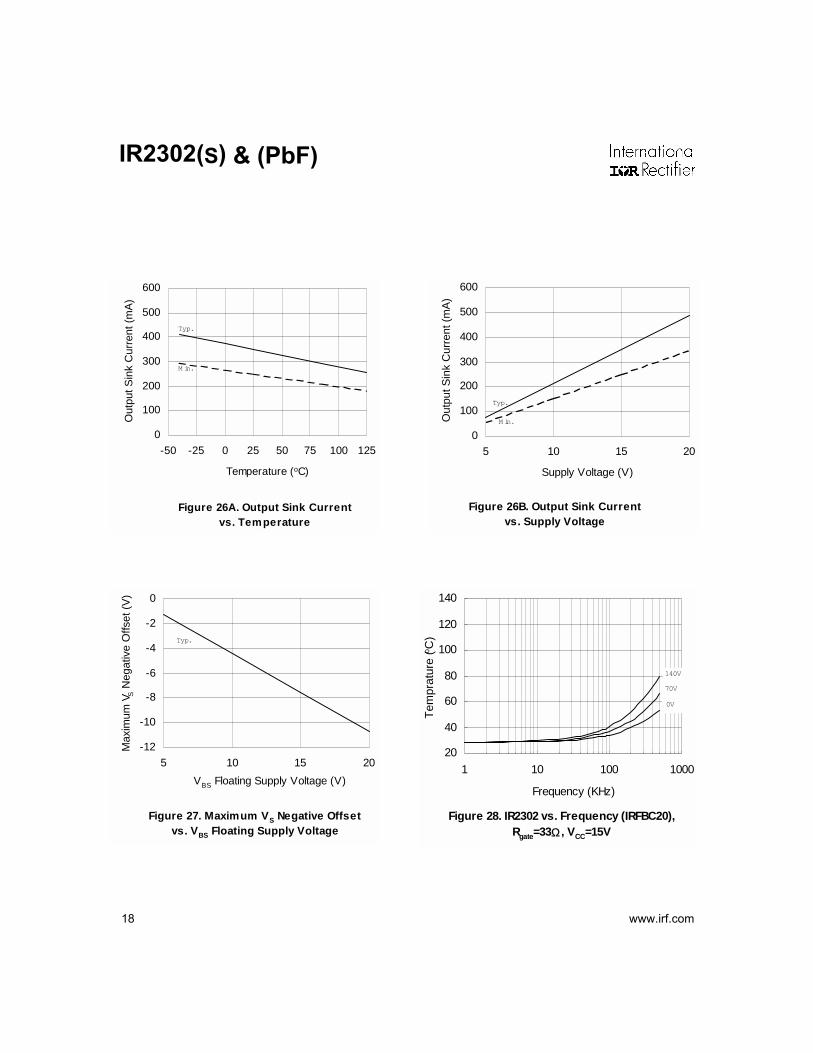
Figure 26A. Output Sink Current vs. Temperature
Typ.
-12
-10
-8
-6
-4
-2
0
5 10 15 20VBS Floating Supply Voltage (V)
Max
imum
VS N
egat
ive
Offs
et (V
)
Figure 27. Maximum VS Negative Offset vs. VBS Floating Supply Voltage
Typ.
0
100
200
300
400
500
600
5 10 15 20
Supply Voltage (V)
Out
put S
ink
Cur
rent
(mA)
Figure 26B. Output Sink Current vs. Supply Voltage
Typ.
M in.
20
40
60
80
100
120
140
1 10 100 1000
Frequency (KHz)
Tem
prat
ure
(o C)
70V
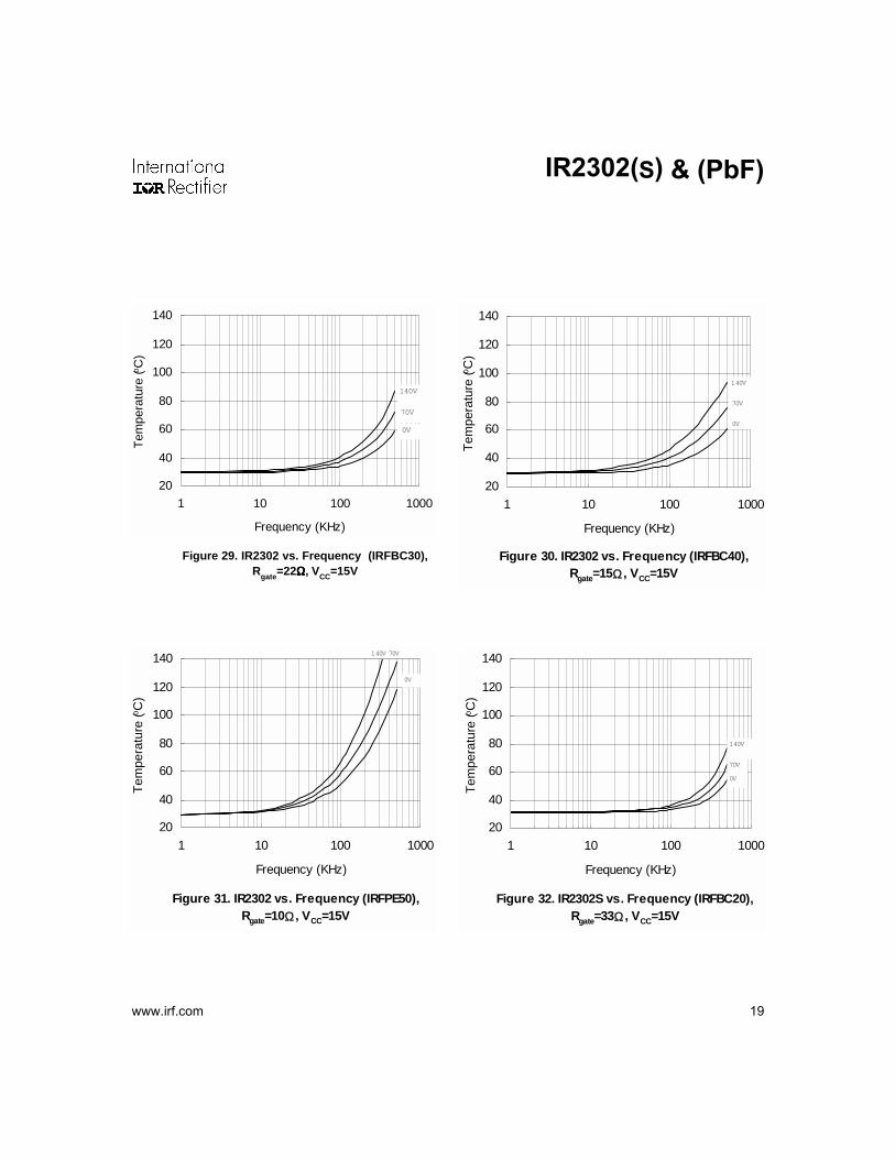
Figure 28. IR2302 vs. Frequency (IRFBC20), Rgate=33Ω , VCC=15V
140V
0V
IR2302(S) & (PbF)
www.irf.com 19
20
40
60
80
100
120
140
1 10 100 1000
Frequency (KHz)
Tem
pera
ture
(o C)
140V
70V
0V
Figure 30. IR2302 vs. Frequency (IRFBC40), Rgate=15Ω , VCC=15V
20
40
60
80
100
120
140
1 10 100 1000
Frequency (KHz)
Tem
pera
ture
(o C)
Figure 31. IR2302 vs. Frequency (IRFPE50), Rgate=10Ω , VCC=15V
0V
140V 70V
20
40
60
80
100
120
140
1 10 100 1000
Frequency (KHz)
Tem
pera
ture
(o C)
Figure 32. IR2302S vs. Frequency (IRFBC20), Rgate=33Ω , VCC=15V
0V
70V
140V
Figure 29. IR2302 vs. Frequency (IRFBC30),Rgate=22ΩΩΩΩΩ, VCC=15V
20
40
60
80
100
120
140
1 10 100 1000
Frequency (KHz)
Tem
pera
ture
(o C)
140V
0V
70V

IR2302(S) & (PbF)
20 www.irf.com
20
40
60
80
100
120
140
1 10 100 1000
Frequency (KHz)
Tem
pera
ture
(o C) 140V
70V
0V
Figure 33. IR2302S vs. Frequency (IRFBC30), Rgate=22Ω , VCC=15V
20
40
60
80
100
120
140
1 10 100 1000
Frequency (KHz)
Tem
pera
ture
(o C)
0V
Figure 34. IR2302S vs. Frequency (IRFBC40), Rgate=15Ω, VCC=15V
140V 70V
20
40
60
80
100
120
140
1 10 100 1000
Frequency (KHz)
Tem
pret
ure
(o C)
Figure 35. IR2302S vs. Frequency (IRFPE50), Rgate=10Ω , VCC=15V
140V 70V 0V

IR2302(S) & (PbF)
www.irf.com 21
Case Outlines
01-602701-0021 11 (MS-012AA)8 Lead SOIC
8 7
5
6 5
D B
E
A
e6X
H
0.25 [.010] A
6
431 2
4. OUTLINE CONFORMS TO JEDEC OUTLINE MS-012AA.
NOTES:1. DIMENSIONING & TOLERANCING PER ASME Y14.5M-1994.2. CONTROLLING DIMENSION: MILLIMETER3. DIMENSIONS ARE SHOWN IN MILLIMETERS [INCHES].
7
K x 45°
8X L 8X c
y
FOOTPRINT
8X 0.72 [.028]
6.46 [.255]
3X 1.27 [.050] 8X 1.78 [.070]
5 DIMENSION DOES NOT INCLUDE MOLD PROTRUSIONS.
6 DIMENSION DOES NOT INCLUDE MOLD PROTRUSIONS. MOLD PROTRUSIONS NOT TO EXCEED 0.25 [.010].7 DIMENSION IS THE LENGTH OF LEAD FOR SOLDERING TO A SUBSTRATE.
MOLD PROTRUSIONS NOT TO EXCEED 0.15 [.006].
0.25 [.010] C A B
e1A
A18X b
C
0.10 [.004]
e 1
D
E
y
b
A
A1
H
K
L
.189
.1497
0°
.013
.050 BASIC
.0532
.0040
.2284
.0099
.016
.1968
.1574
8°
.020
.0688
.0098
.2440
.0196
.050
4.80
3.80
0.33
1.35
0.10
5.80
0.25
0.40
0°
1.27 BASIC
5.00
4.00
0.51
1.75
0.25
6.20
0.50
1.27
MIN MAXMILLIMETERSINCHESMIN MAX
DIM
8°
e
c .0075 .0098 0.19 0.25
.025 BASIC 0.635 BASIC
01-601401-3003 01 (MS-001AB)8 Lead PDIP

IR2302(S) & (PbF)
22 www.irf.com
Basic Part (Non-Lead Free)8-Lead PDIP IR2302 order IR23028-Lead SOIC IR2302S order IR2302S
Leadfree Part8-Lead PDIP R2302 not available8-Lead SOIC IR2302S order IR2302SPbF
ORDER INFORMATION
LEADFREE PART MARKING INFORMATION
Lead Free ReleasedNon-Lead FreeReleased
Part number
Date code
IRxxxxxx
YWW?
?XXXXPin 1Identifier
IR logo
Lot Code(Prod mode - 4 digit SPN code)
Assembly site codePer SCOP 200-002
P? MARKING CODE
Thisproduct has been designed and qualified for the Industrial market.Qualification Standards can be found on IR’s Web Site http://www.irf.com
Data and specifications subject to change without notice.IR WORLD HEADQUARTERS: 233 Kansas St., El Segundo, California 90245 Tel: (310) 252-7105
8/16/2004