Braj Bhasha Soor Kosh Part-6, Deendayal Gupta, 200p, Language. Linguistics. Literature, Hindi

ERTEC 200P Enhanced Real-Time Ethernet Controller
DATA SHEET
Features
Integrated processor ARM926EJ-S
125 / 250 MHz Core Frequency 16 KB Data-Cache 16 KB Instruction-Cache 256 KB TCM-RAM 8 KB Boot ROM Little Endian
System Bus Structure 32 Bit / 125 MHz AHB Bus Multi-Layer AHB Lite with 7
Masters and 12 Slaves AHB Address Range Monitoring
Local Bus Unit (XHIF) Allows External Master to access
internal ERTEC 200P registers 16 / 32-Bit Data Bus 2 x 4 Paging Registers
Memory Controller (EMC) 8 / 16 / 32 Bit Data Bus 4 chip selects Supports SDRAM, SRAM, Burst
Mode Flash ROM
Onchip Peripherals
DMA Controller 6 Timers 2 Watchdogs
I/O Interfaces
2 x 2 SPI Interfaces 4 UARTs 1 I²C-Interface One 96-bit GPIO Port 1,8 / 3,3 V I/O Buffers
Test / Debug Functionality
Boundary Scan
Integrated Ethernet-Phy 2 Ports Supports 100Base-TX and -FX Auto Cross Over Auto MDIX Jitter free Latency
Package 400 Pin FPBGA Size 17mm x 17 mm Ball Pitch 0,8mm

Copyright © Siemens AG 2014. All rights reserved. 2 ERTEC 200P Data Sheet Technical data subject to change. Version 1.1
Disclaimer of Liability We have checked the contents of this manual for agreement with the hardware and software described. Since deviations cannot be precluded entirely, we cannot guarantee full agreement. However, the data in this manual are reviewed regularly. Necessary corrections are included in subsequent editions. Suggestions for improvement are welcomed. Copyright © Siemens AG 2014. All rights reserved The reproduction, transmission or use of this document or its contents is not permitted without express written authority. Offenders will be liable for damages. All rights, including rights created by patent grant or registration of a utility model or design, are reserved. All product and system names are registered trademarks of their respective owner and must be treated as such. Technical data subject to change.
Additional Support If you have questions regarding use of the described block that are not addressed in the documentation, please contact your Siemens representative.
Please send your written questions, comments, and suggestions regarding the data sheet to the hotline via the e-mail address indicated above.
In addition, you can receive general information, current product information, FAQs, and downloads pertaining to your application on the Internet at:
http://www.siemens.com/comdec
Technical Contacts for Germany / Worldwide
Siemens AG Automation & Drives ComDeC
Phone: 0911/750-2080 Fax: 0911/750-2100 E-mail: [email protected]
Street address: Würzburgerstr.121 90766 Fürth Federal Republic of Germany
Mailing address: P.O. Box 2355 90713 Fürth Federal Republic of Germany
Technical Contacts for USA PROFI Interface Center: One Internet Plaza PO Box 4991 Johnson City, TN 37602-4991
Fax: +1(423)- 262- 2103 Phone: +1(423)- 262- 2576 E-mail: [email protected]
Copyright © Siemens AG 2014. All rights reserved. 3 ERTEC 200P Data Sheet Technical data subject to change. Version 1.1
Contents 1. Functional Overview 7 1.1 Key Functional Units 7 1.1.1 Processor Core Subsystem (ARM926) 7 1.1.2 Processor Bus Unit 8 1.1.3 PROFINET–IP (PN-IP) 8 1.1.4 Peripheral Interface (PER-IF) 8 2 Pin Description 9 2.1 Signal Table 9 2.1.1 Signalgroup "System" 9 2.1.2 Signalgroup “Test” 9 2.1.3 Signalgroup “PHY” 10 2.1.4 Signalgroup "JTAG-Ports" 10 2.1.5 Signalgroup “GPIO-Ports” 13 2.1.6 Signalgroup “Host Interface” 14 2.2 Power / GND Pins 16 2.3 Handling of Unused Pins 17 3 Maximum Ratings 19 4 AC- and DC-Characteristics 20 4.1 Power Dissipation 20 4.2 DC Operating Conditions 21 5 AC-Parameter (Timing, Constraining) 23 5.1 EMC Interface 23 5.1.1 SDRAM Interface 23 5.1.1.1 SDRAM Timing for a read access 24 5.1.1.2 SDRAM Timing for write access 25 5.1.2 SRAM Interface 26 5.1.2.1 SRAM Timing for a read access 26 5.1.2.2 SRAM Timing for a write access 27 5.1.3 BurstFlash Interface 28 5.2 Host-Interface(XHIF) 29 5.3 SPI Interfaces 30 5.4 PNPLL 31 5.5 Time-Sync Interface 32 5.6 JTAG-Interface 32 5.7 Trace-Interface 33 6 Design Considerations 34 6.1 Power Sequence 34 6.2 ERTEC 200P Design recommendations 35 6.2.1 Design recommendations for ERTEC 200P EMC Bus 35 6.2.1.1 Possible ERTEC 200P EMC configurations 35 6.2.1.2 ERTEC 200P EMC recommendations 36 6.2.1.3 Controlling of an external Level-Shifter 37 6.2.2 Design Recommendations ERTEC 200P supply voltages pins 37 6.2.3 Design Recommendations for ERTEC 200P Profinet PHYs 37 6.2.3.1 ERTEC 200P PHY supply voltages pins 37 6.2.3.2 Filtering on ERTEC 200P PHY supply voltages 38 6.2.3.3 Decoupling on ERTEC 200P PHY supply voltages 39 6.2.4 ERTEC 200P PROFINET TX circuit 40 6.2.4.1 ERTEC 200P PROFINET TX circuit unused pins 41 6.2.5 ERTEC 200P PROFINET FX circuit 42 6.2.5.1 ERTEC 200P/ Avago QFBR-5978AZ SD circuit 43 6.2.5.2 ERTEC 200P PROFINET FX circuit unused pins 44 6.3 Clocking 45 6.3.1 Oscillator 45 6.3.2 External clock source 46 6.3.3 PLL Power Supply 46
Copyright © Siemens AG 2014. All rights reserved. 4 ERTEC 200P Data Sheet Technical data subject to change. Version 1.1
6.4 Reset 48 6.4.1 Power-On Reset Behaviour 48 6.4.2 Strapping Pins 49 6.4.3 Reset Structure 49 6.4.3.1 Asynchronous PowerOn-Reset 50 6.4.3.2 Asynchronous Hardware-Reset 50 6.4.3.3 Asynchronous JTAG-Reset 50 6.4.3.4 Asynchronous ARM926 Watchdog-Reset 51 6.4.3.5 Asynchronous Software-Reset for the ERTEC 200P (without PN-IP) 51 6.4.3.6 Asynchronous Software-Reset of the PN-IP 51 6.4.3.7 Asynchronous Software-Reset of the ARM926EJ-S Core 51 6.4.3.8 Synchronous Software-Reset (PN-IP, PER-IF, Hostinterface) 51 6.5 GPIO Pins 53 6.6 Pull-Up / Pull-Down Resistors 53 6.7 Debug 54 7 Basic Configuration 54 7.1 Address Map 54 7.2 Interrupts 54 7.3 DMA Requests 54 7.4 Timers 54 7.5 GPIO Pin Mapping 54 7.6 Configuration Pins 56 7.7 Boot Pins 56 7.7.1 StartUp-Times 57 8 Thermal Specification 58 9 Package Information 59 9.1 Ordering Info / Part Numbers 59 9.2 400-Pin SIP-FPBGA Package 60 9.3 Soldering Conditions 61 9.4 Packing Information 61 9.5 Ballout 62 10 Quality Information 62 10.1 Life time / (HW) FIT-Rate 62 11 Literature / References 62
Copyright © Siemens AG 2014. All rights reserved. 5 ERTEC 200P Data Sheet Technical data subject to change. Version 1.1
List of Figures
Figure 1: ERTEC 200P Blockdiagram 7 Figure 2: SDRAM – Timing for a read access 24 Figure 3: SDRAM – Timing for a write access 25 Figure 4: SRAM – Timing for a read access 26 Figure 5: SRAM – Timing for a write access 27 Figure 6: BurstFlash – Timing for a read-burst 28 Figure 7: XHIF - Sequence for a read access 29 Figure 8: XHIF - Sequence for a write access 29 Figure 9: Debug Interface 32 Figure 10: ARM926 Trace Interface 33 Figure 11: Power Sequence example 34 Figure 12: EMC Bus configurations 35 Figure 13: PHY power filtering 38 Figure 14: PI Filter 39 Figure 15: PHY decoupling 40 Figure 16: UTP circuit 41 Figure 17: UTP circuit unused 42 Figure 18: FX circuit 43 Figure 19: SD level translation circuit 44 Figure 20: FX circuit unused pins 44 Figure 21: Oscillator Circuitry 45 Figure 22 : Oscillator Circuitry Layout Example 46 Figure 23: Recommended for PLL Power Supply Filter 47 Figure 24: Power-On Reset Behaviour 48 Figure 25: Timing reset 49 Figure 26: StartUp of the PLL 50 Figure 27: Single GPIO Cell 53 Figure 28: Package Information 60 Figure 29: Ballout ERTEC 200P 62 List of Tables Table 1: External Pull wiring for the JTAG-Interface 11 Table 2: Maximum Ratings 19 Table 3: Power Dissipation TX mode 20 Table 4: Power Dissipation FX mode 21 Table 5: DC Operating Conditions 22 Table 6: Definition of SDRAM commands 23 Table 7: Timing for a SDRAM read access 24 Table 8: Timing for a SDRAM write access 25 Table 9: Timing for a SRAM read access 26 Table 10: Timing for a SRAM write access 27 Table 11: Timing for a BurstFlash read-burst 28 Table 12: Timing for a XHIF read access 29 Table 13: Timing for a XHIF write access 30 Table 14: Timing for a SPI access 31 Table 15: Timing PNPLL Interface 32 Table 16: Timing Time-Sync Interface 32 Table 17: Velocity/ impedance on traces 35 Table 18: Min/ max trace length 36 Table 19: Minimal reset duration 48 Table 20: Pull-Up / Pull-Down Resistor Values 53 Table 21: GPIO Port 0 Input Mapping 54 Table 22: GPIO Port 1 Input Mapping 55 Table 23: GPIO Port 2 Input Mapping 56 Table 24: Configuration Pins 56 Table 25: Boot Pins 57 Table 26: StartUp-Times 57
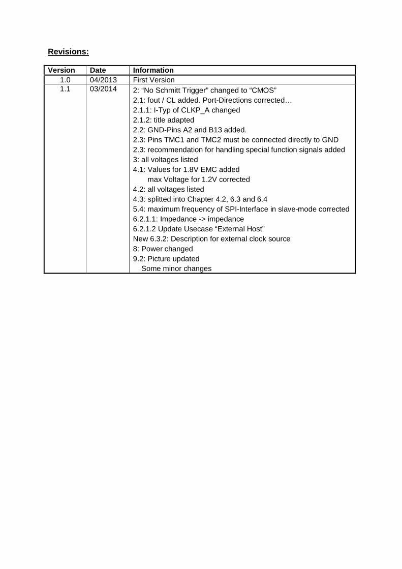
Revisions: Version Date Information
1.0 04/2013 First Version 1.1 03/2014 2: “No Schmitt Trigger” changed to “CMOS”
2.1: fout / CL added. Port-Directions corrected… 2.1.1: I-Typ of CLKP_A changed 2.1.2: title adapted 2.2: GND-Pins A2 and B13 added. 2.3: Pins TMC1 and TMC2 must be connected directly to GND 2.3: recommendation for handling special function signals added 3: all voltages listed 4.1: Values for 1.8V EMC added max Voltage for 1.2V corrected 4.2: all voltages listed 4.3: splitted into Chapter 4.2, 6.3 and 6.4 5.4: maximum frequency of SPI-Interface in slave-mode corrected 6.2.1.1: Impedance -> impedance 6.2.1.2 Update Usecase “External Host” New 6.3.2: Description for external clock source 8: Power changed 9.2: Picture updated Some minor changes

Copyright © Siemens AG 2014. All rights reserved. 7 ERTEC 200P Data Sheet Technical data subject to change. Version 1.1
1. Functional Overview
MU
X/A
rb.
MU
X
Sla
ve
Mas
ter
Sla
ve
Sla
veS
lave
Sla
veS
lave
Per
iphe
ral P
orts
AP
B
(125
MH
z, 3
2Bit)
Sla
ve
Sla
veS
lave
OU
TIN
IN
JTA
GJT
AG
250M
Hz
125M
Hz
Sla
ve
Trac
e
Sla
ve
Figure 1: ERTEC 200P Blockdiagram
1.1 Key Functional Units
1.1.1 Processor Core Subsystem (ARM926)
ARM926EJ-S Processor Core 8 Kbyte Boot ROM 256 Kbyte TCM-RAM
- EDC with 1-Bit Error Correction and 2-Bit Error Detection, with byte access - configurable as Data (256-0) or Instruction (0-256)-RAM - configuration-step: 64 Kbyte
ARM Interrupt Controller - max. 96 Interrupts - max. 8 fast Interrupts - 8 Software Interrupt inputs and 86 Hardware Interrupt inputs
Embedded Trace Macrocell (ETM9, see /2/) for Debugging JTAG Block for Debugging Memory Management Unit (MMU) with Translation Lookaside Buffers (TLBs) Separate Data and Instruction-Bus

Copyright © Siemens AG 2014. All rights reserved. 8 ERTEC 200P Data Sheet Technical data subject to change. Version 1.1
1.1.2 Processor Bus Unit
Memory Controller (EMC) - SDRAM-Controller features:
16 / 32 bit databus width PC133 SDRAM-compatible (125 MHz synchron is used) 1 Bank with max. 256 MByte SDRAM (32 Bit databus) SDRAM support for following parts:
CAS-Latency: 2 or 3 clocks Bank-address bits (1/2/4 internal banks), realized via the lowest two bits of the
address bus MA(1:0) 8 / 9 / 10 / 11 bits column-address MA(13), MA(11:2) max. 14 bits row-address MA(15:2)
- Asynchronous controller features: 8 / 16 / 32 bit bus width (for each chip select programmable) 4 chip selects the timing for each chip select can be set individually the response to ready signal can be set individually for each chip select a maximum of 64 MByte address area for each chip select
DMA Controller - 1 Channel - 31 Jobs
20 can be started from hardware 31 can be started from software
Two SPI Interfaces - SPI1 via dedicated Pins - SPI2 via GPIO Pins
UART Interface via dedicated Pins Timer Unit (Module TIMER_TOP)
- … reloadable Down-Counters - each Timer is equipped with a Multiplexer for Trigger Signals
Interrupt Control Unit (Module ICU) - level or edge triggered Operation - 96 Interrupt Request Inputs - Interrupt Priority is individually selectable for each Request Input
Watchdog Unit (Module WDG1) - Watchdog Interrupt Generation via Counter 0 - Watchdog Reset Generation via Counter 1 - Once started, the watchdog can only be stopped by a Power-On Reset.
1.1.3 PROFINET–IP (PN-IP)
2 Ethernet-Ports 100MBit/s Ethernet-Port with integrated dual PHY Dynamic Frame Packing Fast Forwarding Short Preamble Dynamic Fragmentation IRT-Forwarding PN-PLL Support for Syncronisation-Protocolls (PTCP)
1.1.4 Peripheral Interface (PER-IF)
Supports Consistency for IO Data

Copyright © Siemens AG 2014. All rights reserved. 9 ERTEC 200P Data Sheet Technical data subject to change. Version 1.1
2 Pin Description In the signal tables, the following abbreviations are used: Abbreviation Description C S OSC
CMOS Input Schmitt Trigger Input Oscillator Input
dn Internal 50 k pull-down resistor up disabled
Internal 50 k pull-up resistor Internal pull is disabled
PECL Positive emitter coupled logic bi Bidirectional Port AO Analog Output AI Analog Input NC n/a -
No connection Not Applicable Not Applicable
Note that signals with the prefix “X” are active low signals.
2.1 Signal Table Hint: If no load capacitance (CL) is specified in the table, a default load of 20 pF is used.
2.1.1 Signalgroup "System" Signal Signaldescription Dir Output
(V) Input (V)
Internal Pull
Current (mA)
I-Typ fout (MHz)
CL/ MAX (pF)
pinid
REF_CLK Reference Clock MII (ext PHY) bi 3.3 3.3 - 6 C 25 50 W16
BYP_CLK F-Timer Clock in - 3.3 - - C T11
XRESET HW-Reset in - 3.3 up - S W15
CLKP_A1) Quartz crystal connection in - 3.3 - - OSC Y14
CLKP_B1) Quartz crystal connection out 3.3 - - 12 - 25 50 W14 1) see Chapter 6.3.1 for recommended crystal or Chapter 6.3.2 for usage of external clock source
2.1.2 Signalgroup “Test” Signal Signaldescription Dir Output
(V) Input (V)
Pull Current (mA)
I-Typ
fout (MHz)
CL/ MAX (pF)
pinid
TEST1) IC-Test-Mode in - 3.3 dn - S R9
TMC11) Testmode_1 in - 3.3 - - C F12
TMC21) Testmode_2 in - 3.3 - - C R14
CTRL_STBY0 Stby for 3V3 GPIO(31:0) in - 3.3 up - S M15
CTRL_STBY1 Stby for 1V8/3V3 GPIO(95:32)/XHIF in - 1.8/3.3 up - S J15
CTRL_STBY2 Stby for 1V8/3V3 GPIO(95:32)/XHIF in - 1.8/3.3 up - S F9
TACT1) TESTACT-TAP-RESET in - 3.3 dn - S R12 1) see Table 2 how to use this pin
Copyright © Siemens AG 2014. All rights reserved. 10 ERTEC 200P Data Sheet Technical data subject to change. Version 1.1
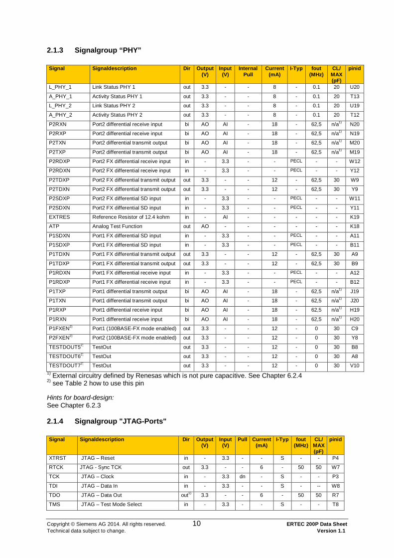
2.1.3 Signalgroup “PHY” Signal Signaldescription Dir Output
(V) Input
(V) Internal
Pull Current
(mA) I-Typ fout
(MHz) CL/
MAX (pF)
pinid
L_PHY_1 Link Status PHY 1 out 3.3 - - 8 - 0.1 20 U20
A_PHY_1 Activity Status PHY 1 out 3.3 - - 8 - 0.1 20 T13
L_PHY_2 Link Status PHY 2 out 3.3 - - 8 - 0.1 20 U19
A_PHY_2 Activity Status PHY 2 out 3.3 - - 8 - 0.1 20 T12
P2RXN Port2 differential receive input bi AO AI - 18 - 62,5 n/a1) N20
P2RXP Port2 differential receive input bi AO AI - 18 - 62,5 n/a1) N19
P2TXN Port2 differential transmit output bi AO AI - 18 - 62,5 n/a1) M20
P2TXP Port2 differential transmit output bi AO AI - 18 - 62,5 n/a1) M19
P2RDXP Port2 FX differential receive input in - 3.3 - - PECL - - W12
P2RDXN Port2 FX differential receive input in - 3.3 - - PECL - - Y12
P2TDXP Port2 FX differential transmit output out 3.3 - - 12 - 62,5 30 W9
P2TDXN Port2 FX differential transmit output out 3.3 - - 12 - 62,5 30 Y9
P2SDXP Port2 FX differential SD input in - 3.3 - - PECL - - W11
P2SDXN Port2 FX differential SD input in - 3.3 - - PECL - - Y11
EXTRES Reference Resistor of 12.4 kohm in - AI - - - - - K19
ATP Analog Test Function out AO - - - - - - K18
P1SDXN Port1 FX differential SD input in - 3.3 - - PECL - - A11
P1SDXP Port1 FX differential SD input in - 3.3 - - PECL - - B11
P1TDXN Port1 FX differential transmit output out 3.3 - - 12 - 62,5 30 A9
P1TDXP Port1 FX differential transmit output out 3.3 - - 12 - 62,5 30 B9
P1RDXN Port1 FX differential receive input in - 3.3 - - PECL - - A12
P1RDXP Port1 FX differential receive input in - 3.3 - - PECL - - B12
P1TXP Port1 differential transmit output bi AO AI - 18 - 62,5 n/a1) J19
P1TXN Port1 differential transmit output bi AO AI - 18 - 62,5 n/a1) J20
P1RXP Port1 differential receive input bi AO AI - 18 - 62,5 n/a1) H19
P1RXN Port1 differential receive input bi AO AI - 18 - 62,5 n/a1) H20
P1FXEN2) Port1 (100BASE-FX mode enabled) out 3.3 - - 12 - 0 30 C9
P2FXEN2) Port2 (100BASE-FX mode enabled) out 3.3 - - 12 - 0 30 Y8
TESTDOUT52) TestOut out 3.3 - - 12 - 0 30 B8
TESTDOUT62) TestOut out 3.3 - - 12 - 0 30 A8
TESTDOUT72) TestOut out 3.3 - - 12 - 0 30 V10 1) External circuitry defined by Renesas which is not pure capacitive. See Chapter 6.2.4 2) see Table 2 how to use this pin Hints for board-design: See Chapter 6.2.3
2.1.4 Signalgroup "JTAG-Ports" Signal Signaldescription Dir Output
(V) Input
(V) Pull Current
(mA) I-Typ fout
(MHz) CL/
MAX (pF)
pinid
XTRST JTAG – Reset in - 3.3 - - S - - P4
RTCK JTAG - Sync TCK out 3.3 - - 6 - 50 50 W7
TCK JTAG – Clock in - 3.3 dn - S - - P3
TDI JTAG – Data In in - 3.3 - - S - -- W8
TDO JTAG – Data Out out1) 3.3 - - 6 - 50 50 R7
TMS JTAG – Test Mode Select in - 3.3 - - S - - T8
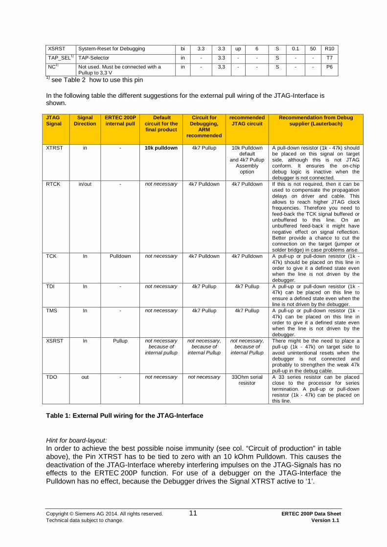
Copyright © Siemens AG 2014. All rights reserved. 11 ERTEC 200P Data Sheet Technical data subject to change. Version 1.1
XSRST System-Reset for Debugging bi 3.3 3.3 up 6 S 0.1 50 R10
TAP_SEL1) TAP-Selector in - 3.3 - - S - - T7
NC1) Not used. Must be connected with a Pullup to 3,3 V
in - 3,3 - - S - - P6
1) see Table 2 how to use this pin In the following table the different suggestions for the external pull wiring of the JTAG-Interface is shown. JTAG Signal
Signal Direction
ERTEC 200P internal pull
Default circuit for the final product
Circuit for Debugging,
ARM recommended
recommended JTAG circuit
Recommendation from Debug supplier (Lauterbach)
XTRST in - 10k pulldown 4k7 Pullup 10k Pulldown default
and 4k7 Pullup Assembly
option
A pull-down resistor (1k - 47k) should be placed on this signal on target side, although this is not JTAG conform. It ensures the on-chip debug logic is inactive when the debugger is not connected.
RTCK in/out - not necessary 4k7 Pulldown 4k7 Pulldown If this is not required, then it can be used to compensate the propagation delays on driver and cable. This allows to reach higher JTAG clock frequencies. Therefore you need to feed-back the TCK signal buffered or unbuffered to this line. On an unbuffered feed-back it might have negative effect on signal reflection. Better provide a chance to cut the connection on the target (jumper or solder bridge) in case problems arise.
TCK In Pulldown not necessary 4k7 Pulldown 4k7 Pulldown A pull-up or pull-down resistor (1k - 47k) should be placed on this line in order to give it a defined state even when the line is not driven by the debugger.
TDI In - not necessary 4k7 Pullup 4k7 Pullup A pull-up or pull-down resistor (1k - 47k) can be placed on this line to ensure a defined state even when the line is not driven by the debugger.
TMS In - not necessary 4k7 Pullup 4k7 Pullup A pull-up or pull-down resistor (1k - 47k) can be placed on this line in order to give it a defined state even when the line is not driven by the debugger.
XSRST In Pullup not necessary because of
internal pullup
not necessary, because of
internal Pullup
not necessary, because of
internal Pullup
There might be the need to place a pull-up (1k - 47k) on target side to avoid unintentional resets when the debugger is not connected and probably to strengthen the weak 47k pull-up in the debug cable.
TDO out - not necessary not necessary 33Ohm serial resistor
A 33 series resistor can be placed close to the processor for series termination. A pull-up or pull-down resistor (1k - 47k) can be placed on this line.
Table 1: External Pull wiring for the JTAG-Interface
Hint for board-layout: In order to achieve the best possible noise immunity (see col. “Circuit of production” in table above), the Pin XTRST has to be tied to zero with an 10 kOhm Pulldown. This causes the deactivation of the JTAG-Interface whereby interfering impulses on the JTAG-Signals has no effects to the ERTEC 200P function. For use of a debugger on the JTAG-Interface the Pulldown has no effect, because the Debugger drives the Signal XTRST active to ‘1’.
Copyright © Siemens AG 2014. All rights reserved. 12 ERTEC 200P Data Sheet Technical data subject to change. Version 1.1
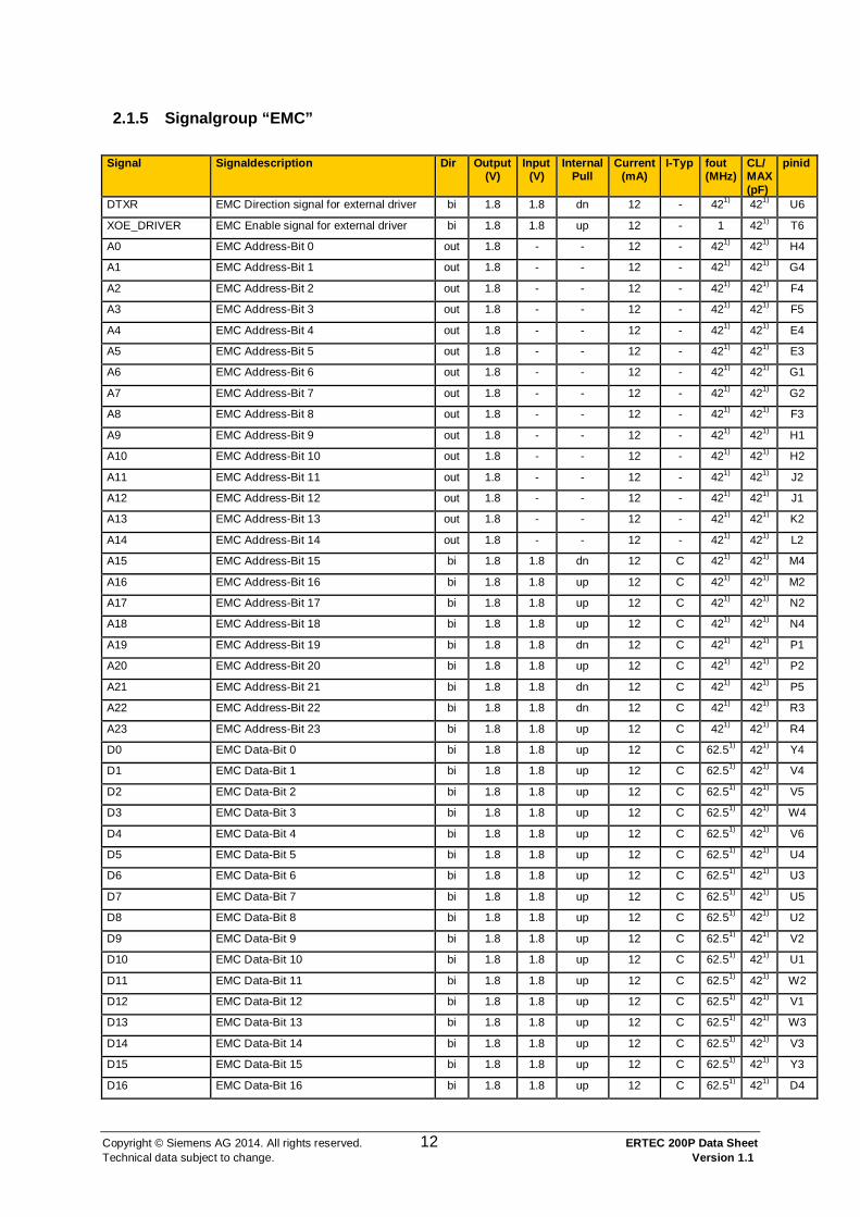
2.1.5 Signalgroup “EMC” Signal Signaldescription Dir Output
(V) Input
(V) Internal
Pull Current
(mA) I-Typ fout
(MHz) CL/ MAX (pF)
pinid
DTXR EMC Direction signal for external driver bi 1.8 1.8 dn 12 - 421) 421) U6
XOE_DRIVER EMC Enable signal for external driver bi 1.8 1.8 up 12 - 1 421) T6
A0 EMC Address-Bit 0 out 1.8 - - 12 - 421) 421) H4
A1 EMC Address-Bit 1 out 1.8 - - 12 - 421) 421) G4
A2 EMC Address-Bit 2 out 1.8 - - 12 - 421) 421) F4
A3 EMC Address-Bit 3 out 1.8 - - 12 - 421) 421) F5
A4 EMC Address-Bit 4 out 1.8 - - 12 - 421) 421) E4
A5 EMC Address-Bit 5 out 1.8 - - 12 - 421) 421) E3
A6 EMC Address-Bit 6 out 1.8 - - 12 - 421) 421) G1
A7 EMC Address-Bit 7 out 1.8 - - 12 - 421) 421) G2
A8 EMC Address-Bit 8 out 1.8 - - 12 - 421) 421) F3
A9 EMC Address-Bit 9 out 1.8 - - 12 - 421) 421) H1
A10 EMC Address-Bit 10 out 1.8 - - 12 - 421) 421) H2
A11 EMC Address-Bit 11 out 1.8 - - 12 - 421) 421) J2
A12 EMC Address-Bit 12 out 1.8 - - 12 - 421) 421) J1
A13 EMC Address-Bit 13 out 1.8 - - 12 - 421) 421) K2
A14 EMC Address-Bit 14 out 1.8 - - 12 - 421) 421) L2
A15 EMC Address-Bit 15 bi 1.8 1.8 dn 12 C 421) 421) M4
A16 EMC Address-Bit 16 bi 1.8 1.8 up 12 C 421) 421) M2
A17 EMC Address-Bit 17 bi 1.8 1.8 up 12 C 421) 421) N2
A18 EMC Address-Bit 18 bi 1.8 1.8 up 12 C 421) 421) N4
A19 EMC Address-Bit 19 bi 1.8 1.8 dn 12 C 421) 421) P1
A20 EMC Address-Bit 20 bi 1.8 1.8 up 12 C 421) 421) P2
A21 EMC Address-Bit 21 bi 1.8 1.8 dn 12 C 421) 421) P5
A22 EMC Address-Bit 22 bi 1.8 1.8 dn 12 C 421) 421) R3
A23 EMC Address-Bit 23 bi 1.8 1.8 up 12 C 421) 421) R4
D0 EMC Data-Bit 0 bi 1.8 1.8 up 12 C 62.51) 421) Y4
D1 EMC Data-Bit 1 bi 1.8 1.8 up 12 C 62.51) 421) V4
D2 EMC Data-Bit 2 bi 1.8 1.8 up 12 C 62.51) 421) V5
D3 EMC Data-Bit 3 bi 1.8 1.8 up 12 C 62.51) 421) W4
D4 EMC Data-Bit 4 bi 1.8 1.8 up 12 C 62.51) 421) V6
D5 EMC Data-Bit 5 bi 1.8 1.8 up 12 C 62.51) 421) U4
D6 EMC Data-Bit 6 bi 1.8 1.8 up 12 C 62.51) 421) U3
D7 EMC Data-Bit 7 bi 1.8 1.8 up 12 C 62.51) 421) U5
D8 EMC Data-Bit 8 bi 1.8 1.8 up 12 C 62.51) 421) U2
D9 EMC Data-Bit 9 bi 1.8 1.8 up 12 C 62.51) 421) V2
D10 EMC Data-Bit 10 bi 1.8 1.8 up 12 C 62.51) 421) U1
D11 EMC Data-Bit 11 bi 1.8 1.8 up 12 C 62.51) 421) W2
D12 EMC Data-Bit 12 bi 1.8 1.8 up 12 C 62.51) 421) V1
D13 EMC Data-Bit 13 bi 1.8 1.8 up 12 C 62.51) 421) W3
D14 EMC Data-Bit 14 bi 1.8 1.8 up 12 C 62.51) 421) V3
D15 EMC Data-Bit 15 bi 1.8 1.8 up 12 C 62.51) 421) Y3
D16 EMC Data-Bit 16 bi 1.8 1.8 up 12 C 62.51) 421) D4
Copyright © Siemens AG 2014. All rights reserved. 13 ERTEC 200P Data Sheet Technical data subject to change. Version 1.1
Signal Signaldescription Dir Output (V)
Input (V)
Internal Pull
Current (mA)
I-Typ fout (MHz)
CL/ MAX (pF)
pinid
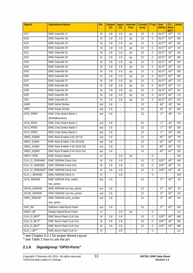
D17 EMC Data-Bit 17 bi 1.8 1.8 up 12 C 62.51) 421) C4
D18 EMC Data-Bit 18 bi 1.8 1.8 up 12 C 62.51) 421) D5
D19 EMC Data-Bit 19 bi 1.8 1.8 up 12 C 62.51) 421) B5
D20 EMC Data-Bit 20 bi 1.8 1.8 up 12 C 62.51) 421) C5
D21 EMC Data-Bit 21 bi 1.8 1.8 up 12 C 62.51) 421) A5
D22 EMC Data-Bit 22 bi 1.8 1.8 up 12 C 62.51) 421) B4
D23 EMC Data-Bit 23 bi 1.8 1.8 up 12 C 62.51) 421) A4
D24 EMC Data-Bit 24 bi 1.8 1.8 up 12 C 62.51) 421) A3
D25 EMC Data-Bit 25 bi 1.8 1.8 up 12 C 62.51) 421) B3
D26 EMC Data-Bit 26 bi 1.8 1.8 up 12 C 62.51) 421) B2
D27 EMC Data-Bit 27 bi 1.8 1.8 up 12 C 62.51) 421) C2
D28 EMC Data-Bit 28 bi 1.8 1.8 up 12 C 62.51) 421) C1
D29 EMC Data-Bit 29 bi 1.8 1.8 up 12 C 62.51) 421) D1
D30 EMC Data-Bit 30 bi 1.8 1.8 up 12 C 62.51) 421) C3
D31 EMC Data-Bit 31 bi 1.8 1.8 up 12 C 62.51) 421) D2
XWR EMC Write Strobe out 1.8 - - 12 - 421 421 N1
XRD EMC Read Strobe out 1.8 - - 12 - 421 421 M1
XCS_PER0 EMC Chip Select Bank 1 out 1.8 - - 12 - 11) 421 T4
(ROM)Bootarea
XCS_PER1 EMC Chip Select Bank 2 out 1.8 - - 12 - 11) 421 R5
XCS_PER2 EMC Chip Select Bank 3 out 1.8 - - 12 - 11) 421 D6
XCS_PER3 EMC Chip Select Bank 4 out 1.8 - - 12 - 11) 421 E6
XBE0_DQM0 EMC Byte Enable 0 für D(7:0) out 1.8 - - 12 - 421) 421) T5
XBE1_DQM1 EMC Byte Enable 1 für D(15:8) out 1.8 - - 12 - 421) 421) T3
XBE2_DQM2 EMC Byte Enable 2 für D(23:16) out 1.8 - - 12 - 421) 421) E5
XBE3_DQM3 EMC Byte Enable 3 für D(31:24) out 1.8 - - 12 - 421) 421) D3
XRDY_PER EMC Ready Signal in - 1.8 up - C - - G6
CLK_O_SDRAM0 EMC SDRAM Clock Out bi 1.8 1.8 - 12 C 1251) 421) H5
CLK_O_SDRAM1 EMC SDRAM Clock Out bi 1.8 1.8 - 12 C 1251) 421) J5
CLK_O_SDRAM22) EMC SDRAM Clock Out bi 1.8 1.8 - 12 C 1251) 421) J6
CLK_I_SDRAM EMC SDRAM Clock In in - 1.8 - - C - - G5
XCS_SDRAM EMC SDRAM chip_select out 1.8 - - 12 - 51) 421) J3
low_active
XRAS_SDRAM EMC SDRAM ras low_active out 1.8 - - 12 - 51) 421) J4
XCAS_SDRAM EMC SDRAM cas low_active out 1.8 - - 12 - 51) 421) K3
XWE_SDRAM EMC SDRAM write_enable out 1.8 - - 12 - 51) 421) K4
low_active
XAV_BF Address Valid Burst Flash out 1.8 - - 12 - 51) 421) K5
XRDY_BF Ready Signal Burst Flash in - 1.8 up - C L4
CLK_O_BF02) EMC Burst Flash CLK Out bi 1.8 1.8 - 12 C 1251) 421) M5
CLK_O_BF12) EMC Burst Flash CLK Out bi 1.8 1.8 - 12 C 1251) 421) N5
CLK_O_BF22) EMC Burst Flash CLK Out bi 1.8 1.8 - 12 C 1251) 421) M6
CLK_I_BF2) EMC Burst Flash CLK In in - 1.8 - - C - - L5 1) see Chapter 6.2.1 for proper Board-Layout 2) see Table 2 how to use the pin
2.1.6 Signalgroup “GPIO-Ports”

Copyright © Siemens AG 2014. All rights reserved. 14 ERTEC 200P Data Sheet Technical data subject to change. Version 1.1
Signal Signaldescription Dir Output
(V) Input
(V) Internal Pull
Current (mA)
I-Typ
fout (MHz)
CL/ MAX (pF)
pinid
GPIO0_INT GPIO (interrupt capable) bi 3.3 3.3 disabled 6 S 25 25 V9
GPIO1_INT GPIO (interrupt capable) bi 3.3 3.3 disabled 6 S 25 25 U7
GPIO2_INT GPIO (interrupt capable ) bi 3.3 3.3 disabled 6 S 25 25 U8
GPIO3_INT GPIO (interrupt capable ) bi 3.3 3.3 disabled 6 S 25 25 U9
GPIO4_INT GPIO (interrupt capable ) bi 3.3 3.3 disabled 6 S 25 25 U10
GPIO5_INT GPIO (interrupt capable ) bi 3.3 3.3 disabled 6 S 25 25 U11
GPIO6_INT GPIO (interrupt capable ) bi 3.3 3.3 disabled 6 S 25 25 U12
GPIO7_INT GPIO (interrupt capable ) bi 3.3 3.3 disabled 6 S 25 25 U13
GPIO8_INT GPIO (interrupt capable ) bi 3.3 3.3 disabled 6 S 25 25 R16
GPIO9_INT GPIO (interrupt capable ) bi 3.3 3.3 disabled 6 S 25 25 R17
GPIO10_INT GPIO (interrupt capable ) bi 3.3 3.3 disabled 6 S 25 25 T16
GPIO11_INT GPIO (interrupt capable ) bi 3.3 3.3 disabled 6 S 25 25 T17
GPIO12_INT GPIO (interrupt capable ) bi 3.3 3.3 dn 6 S 25 25 T18
GPIO13_INT GPIO (interrupt capable ) bi 3.3 3.3 dn 6 S 25 25 U17
GPIO14_INT GPIO (interrupt capable ) bi 3.3 3.3 up 6 S 25 25 U18
GPIO15_INT GPIO (interrupt capable ) bi 3.3 3.3 up 6 S 25 25 V17
GPIO16 GPIO bi 3.3 3.3 dn 6 S 25 20 T9
GPIO17 GPIO bi 3.3 3.3 dn 6 S 25 20 T10
GPIO18 GPIO bi 3.3 3.3 disabled 6 S 25 20 T14
GPIO19 GPIO bi 3.3 3.3 disabled 6 S 25 20 T15
GPIO20 GPIO bi 3.3 3.3 dn 6 S 25 20 U14
GPIO21 GPIO bi 3.3 3.3 up 6 S 25 20 U15
GPIO22 GPIO bi 3.3 3.3 up 6 S 25 20 R18
GPIO23 GPIO bi 3.3 3.3 dn 6 S 25 20 U16
GPIO24 GPIO bi 3.3 3.3 dn 6 S 25 20 W19
GPIO25 GPIO bi 3.3 3.3 dn 6 S 25 20 W18
GPIO26 GPIO bi 3.3 3.3 up 6 S 25 20 W17
GPIO27 GPIO bi 3.3 3.3 up 6 S 25 20 V20
GPIO28 GPIO bi 3.3 3.3 dn 6 S 25 20 Y18
GPIO29 GPIO bi 3.3 3.3 dn 6 S 25 20 Y17
GPIO30 GPIO bi 3.3 3.3 dn 6 S 25 20 V19
GPIO31 GPIO bi 3.3 3.3 dn 6 S 25 20 V18 1) The pull-direction depends on the used Configuration. See Chapter 7.6 Hint: 64 additional GPIO’s are multiplexed with the XHIF-Interface.
2.1.7 Signalgroup “Host Interface” Hint: This table shows the configuration of GPIO95 to 32 used as XHIF Signal Signaldescription Di
r Output
(V) Input
(V) Internal
Pull1) Current
(mA) I-
Typ fout (MHz)
CL/ MAX (pF)
pinid
XHIF_A1 XHIF Address-Bit 1 bi 1.8/3.3 1.8/3.3 up 42)/9 S 25 20 A16
XHIF_A2 XHIF Address-Bit 2 bi 1.8/3.3 1.8/3.3 up 42)/9 S 25 20 C15
XHIF_A3 XHIF Address-Bit 3 bi 1.8/3.3 1.8/3.3 up 42)/9 S 25 20 B16
XHIF_A4 XHIF Address-Bit 4 bi 1.8/3.3 1.8/3.3 up 42)/9 S 25 20 E15
XHIF_A5 XHIF Address-Bit 5 bi 1.8/3.3 1.8/3.3 up 42)/9 S 25 20 D15

Copyright © Siemens AG 2014. All rights reserved. 15 ERTEC 200P Data Sheet Technical data subject to change. Version 1.1
Signal Signaldescription Dir
Output (V)
Input (V)
Internal Pull1)
Current (mA)
I-Typ
fout (MHz)
CL/ MAX (pF)
pinid
XHIF_A6 XHIF Address-Bit 6 bi 1.8/3.3 1.8/3.3 up 42)/9 S 25 20 C17
XHIF_A7 XHIF Address-Bit 7 bi 1.8/3.3 1.8/3.3 up 42)/9 S 25 20 E16
XHIF_A8 XHIF Address-Bit 8 bi 1.8/3.3 1.8/3.3 up 42)/9 S 25 20 B14
XHIF_A9 XHIF Address-Bit 9 bi 1.8/3.3 1.8/3.3 up 42)/9 S 25 20 E17
XHIF_A10 XHIF Address-Bit 10 bi 1.8/3.3 1.8/3.3 up 42)/9 S 25 20 B19
XHIF_A11 XHIF Address-Bit 11 bi 1.8/3.3 1.8/3.3 up 42)/9 S 25 20 C18
XHIF_A12 XHIF Address-Bit 12 bi 1.8/3.3 1.8/3.3 up 42)/9 S 25 20 C19
XHIF_A13 XHIF Address-Bit 13 bi 1.8/3.3 1.8/3.3 up 42)/9 S 25 20 B15
XHIF_A14 XHIF Address-Bit 14 bi 1.8/3.3 1.8/3.3 up 42)/9 S 25 20 C13
XHIF_A15 XHIF Address-Bit 15 bi 1.8/3.3 1.8/3.3 up 42)/9 S 25 20 D17
XHIF_A16 XHIF Address-Bit 16 bi 1.8/3.3 1.8/3.3 up 42)/9 S 25 20 C16
XHIF_A17 XHIF Address-Bit 17 bi 1.8/3.3 1.8/3.3 up 42)/9 S 25 20 A15
XHIF_A18 XHIF Address-Bit 18 bi 1.8/3.3 1.8/3.3 up 42)/9 S 25 20 B18
XHIF_A19 XHIF Address-Bit 19 bi 1.8/3.3 1.8/3.3 up 42)/9 S 25 20 D19
XHIF_SEG_2 XHIF Segment-Bit 2 bi 1.8/3.3 1.8/3.3 up 42)/9 S 25 20 D16
XHIF_SEG_0 XHIF Segment-Bit 0 bi 1.8/3.3 1.8/3.3 up 42)/9 S 25 20 E18
XHIF_SEG_1 XHIF Segment-Bit 1 bi 1.8/3.3 1.8/3.3 up 42)/9 S 25 20 D18
XHIF_XRDY XHIF Ready Signal bi 1.8/3.3 1.8/3.3 -3) 42)/9 S 25 20 L15
XHIF_XIRQ XHIF Interrupt bi 1.8/3.3 1.8/3.3 -3) 42)/9 S 25 20 G15
XHIF_XWR XHIF Write Strobe bi 1.8/3.3 1.8/3.3 up 42)/9 S 25 20 D20
XHIF_XRD XHIF Read Strobe bi 1.8/3.3 1.8/3.3 up 42)/9 S 25 20 C20
XHIF_XCS_R_A20 XHIF Chip Select Register (Config) /A20
bi 1.8/3.3 1.8/3.3 up 42)/9 S 25 20 B17
XHIF_XCS_M XHIF Chip Select Memory bi 1.8/3.3 1.8/3.3 up 42)/9 S 25 20 A17
XHIF_XBE0 XHIF Byte Enable 0 of D(7:0)
bi 1.8/3.3 1.8/3.3 up 42)/9 S 25 20 F16
XHIF_XBE1 XHIF Byte Enable 1 of D(15:8)
bi 1.8/3.3 1.8/3.3 up 42)/9 S 25 20 F17
XHIF_XBE2 XHIF Byte Enable 2 of D(23:16)
bi 1.8/3.3 1.8/3.3 up 42)/9 S 25 20 E14
XHIF_XBE3 XHIF Byte Enable 3 of D(31:24)
bi 1.8/3.3 1.8/3.3 up 42)/9 S 25 20 F14
XHIF_D0 XHIF Data-Bit 0 bi 1.8/3.3 1.8/3.3 up 42)/9 S 25 20 G17
XHIF_D1 XHIF Data-Bit 1 bi 1.8/3.3 1.8/3.3 up 42)/9 S 25 20 L17
XHIF_D2 XHIF Data-Bit 2 bi 1.8/3.3 1.8/3.3 up 42)/9 S 25 20 P17
XHIF_D3 XHIF Data-Bit 3 bi 1.8/3.3 1.8/3.3 up 42)/9 S 25 20 G16
XHIF_D4 XHIF Data-Bit 4 bi 1.8/3.3 1.8/3.3 up 42)/9 S 25 20 H17
XHIF_D5 XHIF Data-Bit 5 bi 1.8/3.3 1.8/3.3 up 42)/9 S 25 20 L16
XHIF_D6 XHIF Data-Bit 6 bi 1.8/3.3 1.8/3.3 up 42)/9 S 25 20 M16
XHIF_D7 XHIF Data-Bit 7 bi 1.8/3.3 1.8/3.3 up 42)/9 S 25 20 K16
XHIF_D8 XHIF Data-Bit 8 bi 1.8/3.3 1.8/3.3 up 42)/9 S 25 20 K17
XHIF_D9 XHIF Data-Bit 9 bi 1.8/3.3 1.8/3.3 up 42)/9 S 25 20 M17
XHIF_D10 XHIF Data-Bit 10 bi 1.8/3.3 1.8/3.3 up 42)/9 S 25 20 N17
XHIF_D11 XHIF Data-Bit 11 bi 1.8/3.3 1.8/3.3 up 42)/9 S 25 20 J16
XHIF_D12 XHIF Data-Bit 12 bi 1.8/3.3 1.8/3.3 up 42)/9 S 25 20 H16
XHIF_D13 XHIF Data-Bit 13 bi 1.8/3.3 1.8/3.3 up 42)/9 S 25 20 N16
XHIF_D14 XHIF Data-Bit 14 bi 1.8/3.3 1.8/3.3 up 42)/9 S 25 20 J17
XHIF_D15 XHIF Data-Bit 15 bi 1.8/3.3 1.8/3.3 up 6/12 - P16

Copyright © Siemens AG 2014. All rights reserved. 16 ERTEC 200P Data Sheet Technical data subject to change. Version 1.1
Signal Signaldescription Dir
Output (V)
Input (V)
Internal Pull1)
Current (mA)
I-Typ
fout (MHz)
CL/ MAX (pF)
pinid
XHIF_D16 XHIF Data-Bit 16 bi 1.8/3.3 1.8/3.3 up 6/12 - E8
XHIF_D17 XHIF Data-Bit 17 bi 1.8/3.3 1.8/3.3 up 6/12 - F7
XHIF_D18 XHIF Data-Bit 18 bi 1.8/3.3 1.8/3.3 up 6/12 - E9
XHIF_D19 XHIF Data-Bit 19 bi 1.8/3.3 1.8/3.3 up 6/12 - D7
XHIF_D20 XHIF Data-Bit 20 bi 1.8/3.3 1.8/3.3 up 6/12 - D8
XHIF_D21 XHIF Data-Bit 21 bi 1.8/3.3 1.8/3.3 up 6/12 - E12
XHIF_D22 XHIF Data-Bit 22 bi 1.8/3.3 1.8/3.3 up 6/12 - D11
XHIF_D23 XHIF Data-Bit 23 bi 1.8/3.3 1.8/3.3 up 6/12 - D9
XHIF_D24 XHIF Data-Bit 24 bi 1.8/3.3 1.8/3.3 up 6/12 - D10
XHIF_D25 XHIF Data-Bit 25 bi 1.8/3.3 1.8/3.3 up 6/12 - E7
XHIF_D26 XHIF Data-Bit 26 bi 1.8/3.3 1.8/3.3 up 6/12 - D13
XHIF_D27 XHIF Data-Bit 27 bi 1.8/3.3 1.8/3.3 up 6/12 - E10
XHIF_D28 XHIF Data-Bit 28 bi 1.8/3.3 1.8/3.3 up 6/12 - D14
XHIF_D29 XHIF Data-Bit 29 bi 1.8/3.3 1.8/3.3 up 6/12 - D12
XHIF_D30 XHIF Data-Bit 30 bi 1.8/3.3 1.8/3.3 up 6/12 - E11
XHIF_D31 XHIF Data-Bit 31 bi 1.8/3.3 1.8/3.3 up 6/12 - E13 1) Pull is not active because Port is configured as Output 2) When operating with 1.8 V the default-Value of the Registers DRIVE47_32GPIO, DRIVE63_48GPIO, DRIVE79_64GPIO and DRIVE95_80GPIO has to be changed from 4mA to 9mA 3) Pull is not active because Port is configured as Output
2.2 Power / GND Pins Pin Ball No. Voltage Description VDD_EMC A1, E1, K1, T1, Y1, Y5, A6, E2,
T2, W5, B6, H6, N6, H7, N7 1.8 V I/O Power Supply (15 Pins) for external memory
controller VDD_XHIF A20, A18, A14, E19, N15, H15,
F13, F8, N14, H14, G13, G8 1.8 / 3.3 V I/O Power Supply (12 Pins) ) for external host
interface VDD12 K7, L7, P10, P11, L14, K14,
G11, G10, K8, L8, N10, N11, L13, K13, H11, H10
1.2 V Core Power Supply (16 Pins)
VDD15 P19, G19, N3, V7, V11, V13, C14, C10, C6
1.5 V PHY Power Supply (9 Pins)
VDD33 Y7, Y16, Y20, W13, T19, G3, M3, F18, C12, C8, K6, R8, R13, P15, F11, P8, P13
3.3 V I/O Power Supply (17 Pins)
GND B1, F1, L1, R1, W1, A2, Y2, Y6, Y10, Y13, Y15, Y19, W20, T20, E20, B20, A19, A13, A10, A7, F2, R2, W6, B7, H3, L3, V8, V12, V16, P18, L18, C11, C7, F6, L6, R6, R11, R15, K15, F15, F10, G7, J7, M7, P7, P9, P12, P14, M14, J14, G14, G12, G9, H8, J8, M8, N8, N9, N12, N13, M13, J13, H13, H12, H9, J9, K9, L9, M9, M10, M11, M12, L12, K12, J12, J11, J10, K10, L10, L11, K11, B13
GND ERTEC 200P-Ground (80 Pins)
PVSSA N18, M18, J18, H18 GND Analog PHY GND, can be shared with VSSAPLLCB. Recommendation: PVSSA should be separated from digital ground by filter or connected to digital ground at far end from ERTEC 200P.
Copyright © Siemens AG 2014. All rights reserved. 17 ERTEC 200P Data Sheet Technical data subject to change. Version 1.1
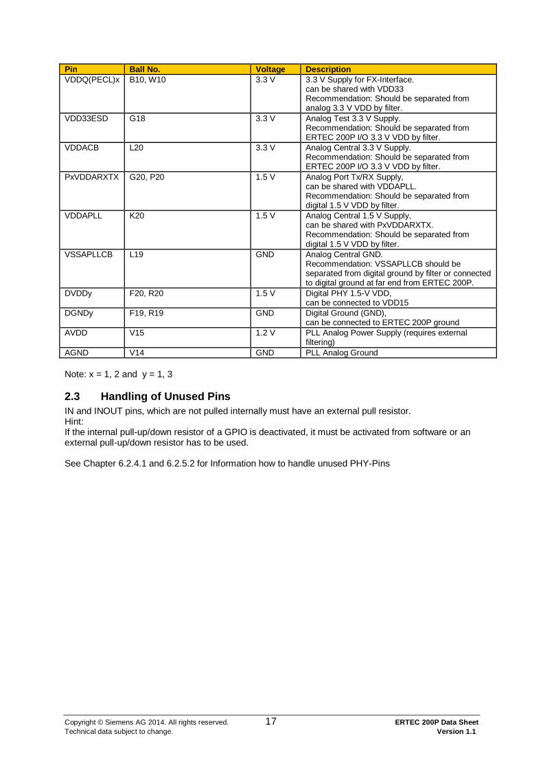
Pin Ball No. Voltage Description VDDQ(PECL)x B10, W10 3.3 V 3.3 V Supply for FX-Interface.
can be shared with VDD33 Recommendation: Should be separated from analog 3.3 V VDD by filter.
VDD33ESD G18 3.3 V Analog Test 3.3 V Supply. Recommendation: Should be separated from ERTEC 200P I/O 3.3 V VDD by filter.
VDDACB L20 3.3 V Analog Central 3.3 V Supply. Recommendation: Should be separated from ERTEC 200P I/O 3.3 V VDD by filter.
PxVDDARXTX G20, P20 1.5 V Analog Port Tx/RX Supply, can be shared with VDDAPLL. Recommendation: Should be separated from digital 1.5 V VDD by filter.
VDDAPLL K20 1.5 V Analog Central 1.5 V Supply, can be shared with PxVDDARXTX. Recommendation: Should be separated from digital 1.5 V VDD by filter.
VSSAPLLCB L19 GND Analog Central GND. Recommendation: VSSAPLLCB should be separated from digital ground by filter or connected to digital ground at far end from ERTEC 200P.
DVDDy F20, R20 1.5 V Digital PHY 1.5-V VDD, can be connected to VDD15
DGNDy F19, R19 GND Digital Ground (GND), can be connected to ERTEC 200P ground
AVDD V15 1.2 V PLL Analog Power Supply (requires external filtering)
AGND V14 GND PLL Analog Ground Note: x = 1, 2 and y = 1, 3
2.3 Handling of Unused Pins IN and INOUT pins, which are not pulled internally must have an external pull resistor. Hint: If the internal pull-up/down resistor of a GPIO is deactivated, it must be activated from software or an external pull-up/down resistor has to be used. See Chapter 6.2.4.1 and 6.2.5.2 for Information how to handle unused PHY-Pins

Copyright © Siemens AG 2014. All rights reserved. 18 ERTEC 200P Data Sheet Technical data subject to change. Version 1.1
Signal Signal description Dir Function description PinID/ Ball
ATP Analog Test Function out Analog Test Enable to monitor or drive specific nodes in the analog circuit during analog test. For debugging purposes it is recommended to have this pin accessable for an oscilloscope on a PCB. This pin is not used in normal operation.
K18
TEST IC-Test-Mode in IC Test Mode Select signal for ASIC test. For normal operation this pin must be connected by a 1k Ohm Pull down resistor to GND.
R9
TMC1 Testmode_1 in Test Mode Control Signal for ASIC test. For normal operation this pin must be connected directly to GND.
F12
TMC2 Testmode_2 in Test Mode Control Signal for ASIC test. For normal operation this pin must be connected directly to GND.
R14
TACT TESTACT-TAP-RESET in Special Test Mode TAP Controller Used for Boundary scan test. For normal operation this pin must be connected by a 1k Ohm Pull down resistor to GND.
R12
TAP_SEL TAP Select in TAP Select Used for Boundary scan test. For normal operation this pin must be connected by a 1k Ohm Pull down resistor to GND.
T7
P1FXEN Port 1 Fiber Optic Enable out Port 1 Fiber Optic Enable This pin is not used and should be unconnected. The Fiber Optic transceiver should be enabled all the time by prober pull resistor.
C9
P2FXEN Port 2 Fiber Optic Enable out Port 2 Fiber Optic Enable This pin is not used and should be unconnected. The Fiber Optic transceiver should be enabled all the time by prober pull resistor.
Y8
TESTDOUT5 Test Output 5 out Test Output 5 This pin is not used and should be unconnected.
B8
TESTDOUT6 Test Output 6 out Test Output 6 This pin is not used and should be unconnected.
A8
TESTDOUT7 Test Output 7 out Test Output 7 This pin is not used and should be unconnected.
V10
CLK_O_SDRAM2 EMC SDRAM Clock Out bi Clock Output SDRAM 2 In normal operation this signal is connected to second SDRAM, upper 16 Bit (see 6.2.1). In case where just one SDRAM is implemented an external 10k Ohm Pull up resistor must be connected.
H5
CLK_O_BF0 EMC Burst Flash CLK Out bi Clock Output Burst Mode Flash 0 In normal operation this signal is connected to CLK_I_BF (see 6.2.1). In case where no Burst Mode Flash is implemented an external 10k Ohm Pull up resistor must be connected.
M5
CLK_O_BF1 EMC Burst Flash CLK Out bi Clock Output Burst Mode Flash 1 In normal operation this signal is connected to first Burst Mode Flash, lower 16 Bit (see 6.2.1). In case where no Burst Mode Flash is implemented an external 10k Ohm Pull up resistor must be connected.
N5
CLK_O_BF2 EMC Burst Flash CLK Out bi
Clock Output Burst Mode Flash 2 In normal operation this signal is connected to
M6
Copyright © Siemens AG 2014. All rights reserved. 19 ERTEC 200P Data Sheet Technical data subject to change. Version 1.1
Signal Signal description Dir Function description PinID/ Ball
second Burst Mode Flash, upper 16 Bit (see 6.2.1). In case where just one Burst Mode Flash is implemented an external 10k Ohm Pull up resistor must be connected.
CLK_I_BF EMC Burst Flash CLK In in Clock Input Burst Mode Flash In normal operation this signal is connected to CLK_O_BF0 (see 6.2.1). In case where no Burst Mode Flash is implemented an external 10k Ohm Pull up resistor must be connected.
L5
NC Reserved in Reserved This pin is not used and must be connected by a 1k Ohm Pull up resistor to VDD33.
P6
Table 2: Recommendation for handling special function signals
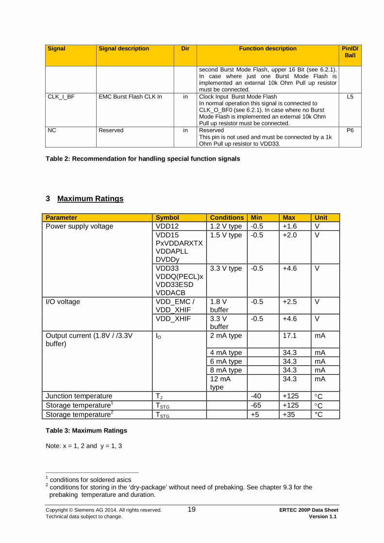
3 Maximum Ratings Parameter Symbol Conditions Min Max Unit Power supply voltage VDD12 1.2 V type -0.5 +1.6 V VDD15
PxVDDARXTX VDDAPLL DVDDy
1.5 V type -0.5 +2.0 V
VDD33 VDDQ(PECL)x VDD33ESD VDDACB
3.3 V type -0.5 +4.6 V
I/O voltage VDD_EMC / VDD_XHIF
1.8 V buffer
-0.5 +2.5 V
VDD_XHIF 3.3 V buffer
-0.5 +4.6 V
Output current (1.8V / /3.3V buffer)
IO 2 mA type 17.1 mA
4 mA type 34.3 mA 6 mA type 34.3 mA 8 mA type 34.3 mA 12 mA
type 34.3 mA
Junction temperature TJ -40 +125 C Storage temperature1 TSTG -65 +125 C Storage temperature2 TSTG +5 +35 °C
Table 3: Maximum Ratings
Note: x = 1, 2 and y = 1, 3
1 conditions for soldered asics 2 conditions for storing in the ‘dry-package’ without need of prebaking. See chapter 9.3 for the prebaking temperature and duration.
Copyright © Siemens AG 2014. All rights reserved. 20 ERTEC 200P Data Sheet Technical data subject to change. Version 1.1
Stresses greater than those listed in above table may cause permanent damage to the device. This is a stress rating only, and functional operation of the device at these or any other conditions outside those indicated in the operational sections of this specification is not implied. Exposure to absolute maximum rating conditions for extended periods may adversely affect reliability.
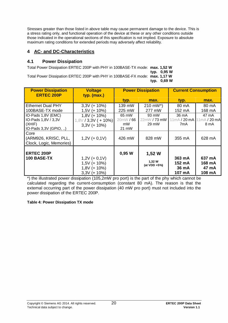
4 AC- and DC-Characteristics
4.1 Power Dissipation Total Power Dissipation ERTEC 200P with PHY in 100BASE-TX mode: max. 1,52 W
typ. 0,95 W Total Power Dissipation ERTEC 200P with PHY in 100BASE-FX mode: max. 1,17 W
typ. 0,69 W
Power Dissipation ERTEC 200P
Voltage typ. (max.)
Power Dissipation Current Consumption
typ. max. typ. max. Ethernet Dual PHY 100BASE-TX mode
3,3V (+ 10%) 1,5V (+ 10%)
139 mW 225 mW
210 mW*) 277 mW
80 mA 152 mA
80 mA 168 mA
IO-Pads 1,8V (EMC) IO-Pads 1,8V / 3,3V (XHIF) IO-Pads 3,3V (GPIO, ..)
1,8V (+ 10%) 1,8V / 3,3V ( + 10%)
3,3V (+ 10%)
65 mW 20mW / 66
mW 21 mW
93 mW 22mW / 73 mW
29 mW
36 mA 11mA / 20 mA
7mA
47 mA 11mA / 20 mA
8 mA
Core (ARM926, KRISC, PLL, Clock, Logic, Memories)
1,2V (+ 0,1V)
426 mW
828 mW
355 mA
628 mA
ERTEC 200P 100 BASE-TX
1,2V (+ 0,1V) 1,5V (+ 10%) 1,8V (+ 10%) 3,3V (+ 10%)
0,95 W
1,52 W
1,32 W
(at VDD +5%)
363 mA 152 mA 36 mA 107 mA
637 mA 168 mA 47 mA 108 mA
*) the illustrated power dissipation (105,2mW pro port) is the part of the phy which cannot be calculated regarding the current-consumption (constant 80 mA). The reason is that the external occurring part of the power dissipation (40 mW pro port) must not included into the power dissipation of the ERTEC 200P. Table 4: Power Dissipation TX mode
Copyright © Siemens AG 2014. All rights reserved. 21 ERTEC 200P Data Sheet Technical data subject to change. Version 1.1
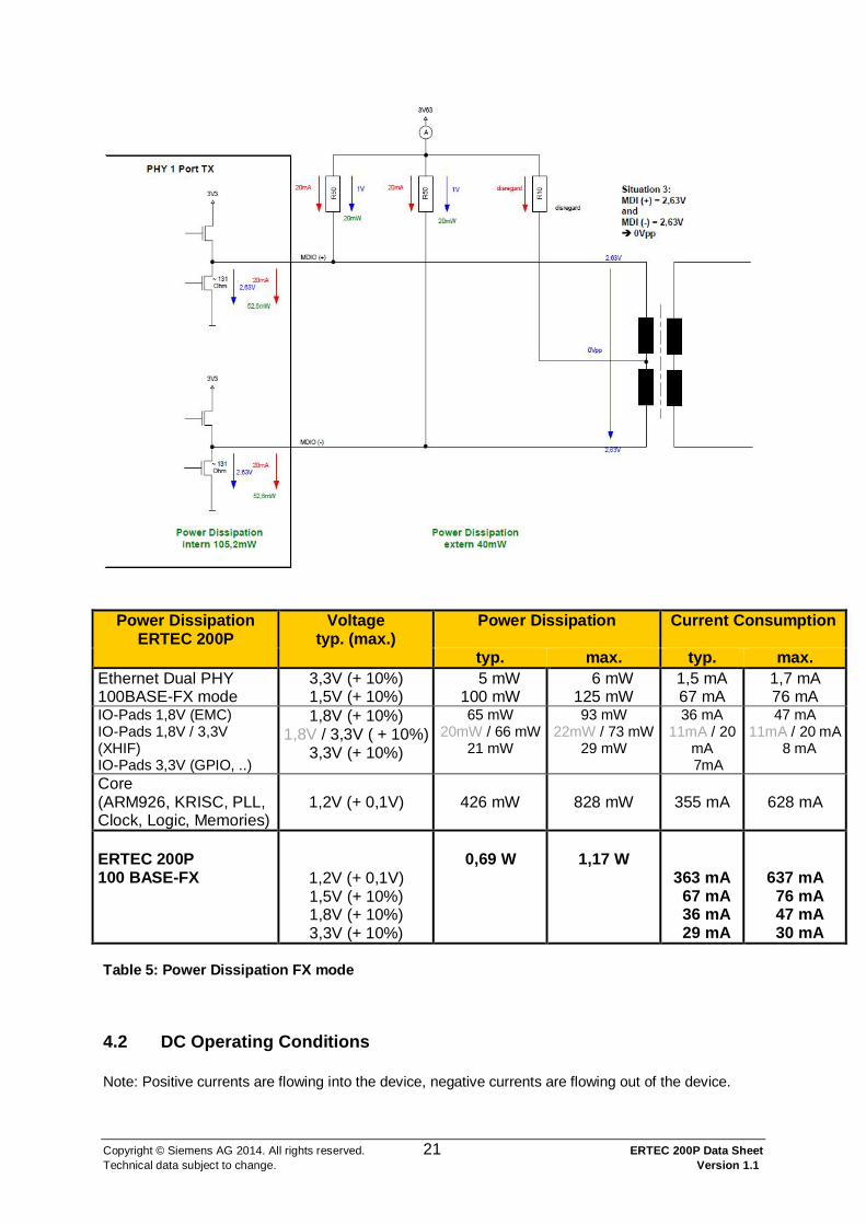
Power Dissipation ERTEC 200P
Voltage typ. (max.)
Power Dissipation Current Consumption
typ. max. typ. max. Ethernet Dual PHY 100BASE-FX mode
3,3V (+ 10%) 1,5V (+ 10%)
5 mW 100 mW
6 mW 125 mW
1,5 mA 67 mA
1,7 mA 76 mA
IO-Pads 1,8V (EMC) IO-Pads 1,8V / 3,3V (XHIF) IO-Pads 3,3V (GPIO, ..)
1,8V (+ 10%) 1,8V / 3,3V ( + 10%)
3,3V (+ 10%)
65 mW 20mW / 66 mW
21 mW
93 mW 22mW / 73 mW
29 mW
36 mA 11mA / 20
mA 7mA
47 mA 11mA / 20 mA
8 mA
Core (ARM926, KRISC, PLL, Clock, Logic, Memories)
1,2V (+ 0,1V)
426 mW
828 mW
355 mA
628 mA
ERTEC 200P 100 BASE-FX
1,2V (+ 0,1V) 1,5V (+ 10%) 1,8V (+ 10%) 3,3V (+ 10%)
0,69 W
1,17 W
363 mA 67 mA 36 mA 29 mA
637 mA 76 mA 47 mA 30 mA
Table 5: Power Dissipation FX mode
4.2 DC Operating Conditions Note: Positive currents are flowing into the device, negative currents are flowing out of the device.

Copyright © Siemens AG 2014. All rights reserved. 22 ERTEC 200P Data Sheet Technical data subject to change. Version 1.1
Parameter Symbol Min Typ Max Unit IO power supply voltage IO power supply voltage
VDD_EMC VDD_XHIF
1,8 – 10% 1,8 1,8 + 10% V
IO power supply voltage IO power supply voltage 3.3 V Supply for FX-Interface
VDD_XHIF VDD33 VDDQ(PECL)x
3,3 – 10% 3,3 3,3 + 10 % V
Core ERTEC 200P Die VDD12 1,1 1,2 1,3 V PLL Analog Power Supply AVDD 1,1 1,2 1,3 V Core PHY Die Digital PHY 1.5-V VDD
VDD15 DVDDy
1,5 – 10 % 1,5 1,5 + 10 % V
Analog Central 1.5 V Supply Analog Port Tx/Rx Supply
VDDAPLL PxVDDARXTX
1,5 – 10 % 1,5 1,5 + 10 % V
Analog Central 3.3 V Supply VDDACB 3,3 – 10 % 3,3 3,3 + 10 % V Analog Test 3.3 V Supply VDD33ESD 3,3 – 10 % 3,3 3,3 + 10 % V Low level input voltage (1.8V) VIL -0.3 VDD x 0.35 V High level input voltage (1.8V) VIH VDD x 0.65 VDD + 0.3 V Low level input voltage (3.3V) VIL -0.3 0.8 V High level input voltage (3.3V) VIH 2.0 VDD + 0.3 V Input rise / fall time 1) tRFIO 0 200 ns fall. trigger voltage (Schmitt, 1.8V) Vifall 0.4 V rise trigger voltage (Schmitt, 1.8V) Virise 1.3 V Hysteresis voltage (Schmitt, 1.8V) VH 0.2 V fall. trigger voltage (Schmitt, 3.3V) Vifall 0.8 V rise trigger voltage (Schmitt, 3.3V) Virise 2 V Hysteresis voltage (Schmitt, 3.3V) VH 0.3 V Input rise / fall time (Schmitt) 1) tRFS 0 1 ms Input current 1.8 V buffer (VIN = 0V or VI = VDD)
IIN ±10 µA
Input current 3.3 V buffer (VIN = 0V or VI = VDD)
IIN ±5 µA
Input current 1.8 V buffer (VIN = 0V, pull-up 50k)
IIN -26 -52 µA
Input current 1.8 V buffer (VIN = VDD, pull-down 50k)
IIN 26 52 µA
Input current 3.3 V buffer (VIN = 0V, pull-up 50k)
IIN -48 -96 µA
Input current 3.3 V buffer (VIN = VDD, pull-down 50k)
IIN 48 96 µA
Output high voltage (IOH = 0 mA) VOH VDD_IO -0.1 V Output low voltage (IOL = 0 mA) VOL 0.1 V Operating ambient temperature Ta -40 +85 C
Table 6: DC Operating Conditions
1) Input voltage rising from 10% to 90% or falling from 90% to 10% of its nominal value Hint: a detailed description of the Power / GND-Pins is listed in Chapter 2.2. The tolerance of the supply voltages includes the ripple on the supply voltage, i.e. the supply voltages including the ripples may not fall under the lower border or rise above the higher border.

Copyright © Siemens AG 2014. All rights reserved. 23 ERTEC 200P Data Sheet Technical data subject to change. Version 1.1
5 AC-Parameter (Timing, Constraining)
5.1 EMC Interface Note: EXTENDED_CONFIG.SODM must be set to 1 to ensure valid timing for the SDRAM data outputs. EXTENDED_CONFIG.BFODM must be set to 1 to ensure valid timing for Burstflash. BF_CONFIG.BF_CLK_F must be kept at 0 to ensure valid timing for Burstflash.
5.1.1 SDRAM Interface The combination of the control signals XCS_DRAM, XRAS_SDRAM, XCAS_SDRAM, XWE_SDRAM and XBEy_DQMy together with the Address bus is defining SDRAM commands in the following way:
SDRAM command
XC
S_S
DR
AM
XR
AS
_SD
RA
M
XC
AS
_SD
RA
M
XW
E_S
DR
AM
XB
Ey_
DQ
My
A Description
COMMAND INHIBIT (NOP) 1 X X X X X No operation NO OPERATION (NOP) 0 1 1 1 X X No operation ACTIVE 0 0 1 1 X BA/Row Select bank and activate row READ 0 1 0 1 1/0 BA/Col Select bank and column, and start READ Burst WRITE 0 1 0 0 1/0 BA/Col Select bank and column, and start WRITE Burst BURST TERMINATE 0 1 1 0 X X Terminate Burst sequence PRECHARGE 0 0 1 0 X Code Deactivate row in bank or banks AUTO REFRESH 0 0 0 1 X X Enter self refresh mode LOAD MODE REGISTER 0 0 0 0 X
Op- Code1 Setup of the device specific configuration register
LOAD EXTENDED MODE REGISTER 0 0 0 0 X
Op- Code2
Setup of the device specific extended mode configuration register (e.g. mobile SDRAM devices)
Table 7: Definition of SDRAM commands
Hint: X meens don’t care. y = 0, 1, 2, 3

Copyright © Siemens AG 2014. All rights reserved. 24 ERTEC 200P Data Sheet Technical data subject to change. Version 1.1
5.1.1.1 SDRAM Timing for a read access The Output-Signals are launched with CLK_O_SDRAMx, the Input-Signals are latched in with CLK_I_SDRAM.
Figure 2: SDRAM – Timing for a read access
Note: The Bank signals BA0, BA1 are part of the address bus A. They are given here separately for a better understanding. Parameter Description Min Max depends on Register tRCD RAS to CAS delay 16 ns 32 ns EXTENDED_CONFIG.TRCD tCAS CAS Latency 16 ns 24 ns SDRAM_CONFIG.CL
Table 8: Timing for a SDRAM read access
Hint: Setup and hold times for address, command and data are the same a by a write access. They can be found in Chapter 5.1.1.2
Copyright © Siemens AG 2014. All rights reserved. 25 ERTEC 200P Data Sheet Technical data subject to change. Version 1.1
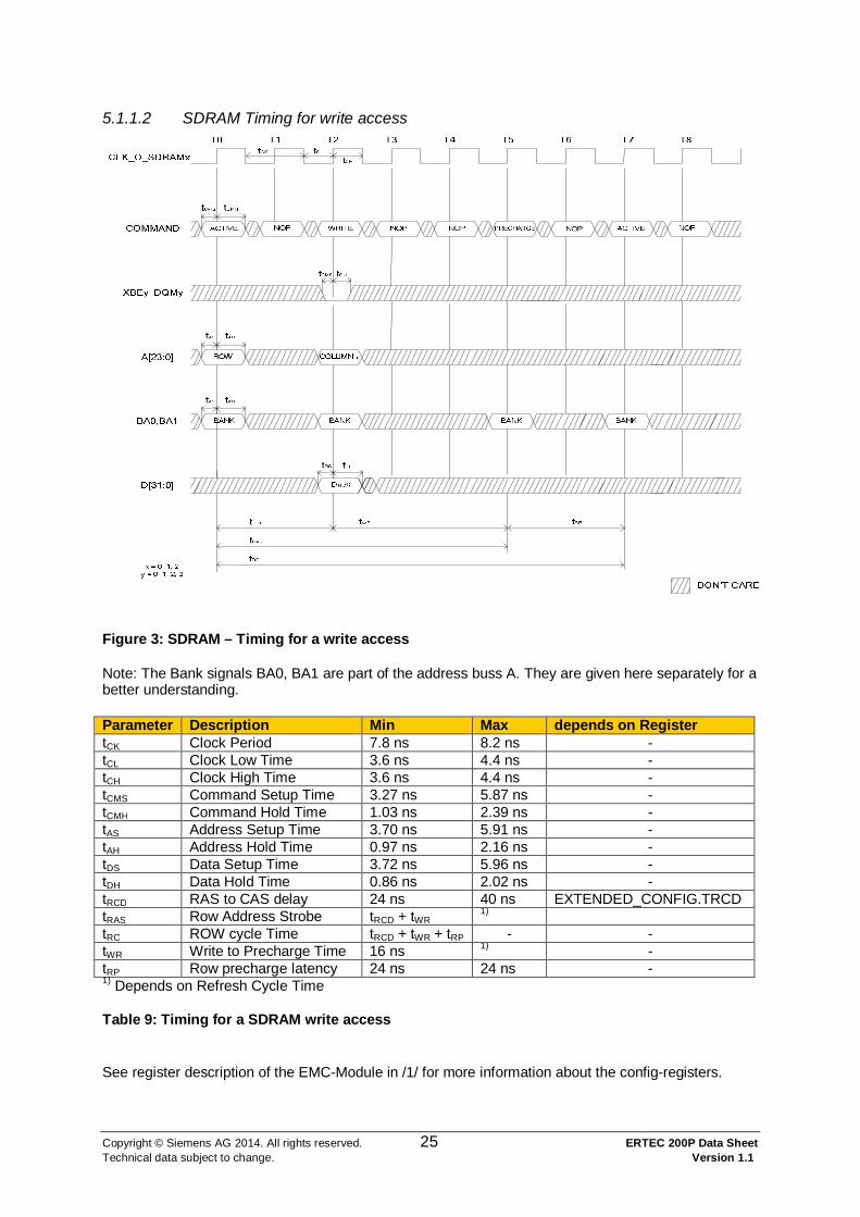
5.1.1.2 SDRAM Timing for write access
Figure 3: SDRAM – Timing for a write access
Note: The Bank signals BA0, BA1 are part of the address buss A. They are given here separately for a better understanding. Parameter Description Min Max depends on Register tCK Clock Period 7.8 ns 8.2 ns - tCL Clock Low Time 3.6 ns 4.4 ns - tCH Clock High Time 3.6 ns 4.4 ns - tCMS Command Setup Time 3.27 ns 5.87 ns - tCMH Command Hold Time 1.03 ns 2.39 ns - tAS Address Setup Time 3.70 ns 5.91 ns - tAH Address Hold Time 0.97 ns 2.16 ns - tDS Data Setup Time 3.72 ns 5.96 ns - tDH Data Hold Time 0.86 ns 2.02 ns - tRCD RAS to CAS delay 24 ns 40 ns EXTENDED_CONFIG.TRCD tRAS Row Address Strobe tRCD + tWR 1) tRC ROW cycle Time tRCD + tWR + tRP - - tWR Write to Precharge Time 16 ns 1) - tRP Row precharge latency 24 ns 24 ns - 1) Depends on Refresh Cycle Time
Table 9: Timing for a SDRAM write access
See register description of the EMC-Module in /1/ for more information about the config-registers.

Copyright © Siemens AG 2014. All rights reserved. 26 ERTEC 200P Data Sheet Technical data subject to change. Version 1.1
5.1.2 SRAM Interface The use of XRDY_PER is optional and can be enabled with ASYNC_BANKx.EW. Wait-States can be inserted if XRDY_PER is used. Hint: For the asynchronous SRAM interface an “active interface” is selectable. Active interface means that at the end of a transfer the data bus is actively driven high for one AHB clock cycle. This is necessary together with the use of internal pullups to speed up the reloading of the wiring capacity. After the active phase the internal pullups are driving the data bus and there is no need for external pullups on the board.
5.1.2.1 SRAM Timing for a read access
A[23:0]
XBEx_DQMx
D[31:0]
XRD (xoe_async)
XRDY_PER
XCS_PERx
Read Data
DTXR
XOE_DRIVER
111...111
tADB
x = 0, 1, 2, 3
tRECOVtR_HOLDtR_STROBEtR_SU
tXRDY
Figure 4: SRAM – Timing for a read access
Parameter Description Min Max depends on Register tR_SU Read Setup-Time 0 ns 120 ns ASYNC_BANKx.R_SU tR_STROBE Read Strobe-Time 8 ns 512 ns ASYNC_BANKx.R_STROBE tR_HOLD Read Hold-Time 8 ns 64 ns ASYNC_BANKx.R_HOLD tXRDY not ready pulse width 16 ns ASYNC_BANKx.EW tADB active data bus 8 ns 8 ns EXTENDED_CONFIG.ADB tRECOV Recovery Phase 0 ns 120 ns RECOV_CONFIG.RECOVx
Table 10: Timing for a SRAM read access
See register description of the EMC-Module in /1/ for more information about the config-registers.

Copyright © Siemens AG 2014. All rights reserved. 27 ERTEC 200P Data Sheet Technical data subject to change. Version 1.1
5.1.2.2 SRAM Timing for a write access
Figure 5: SRAM – Timing for a write access
Parameter Description Min Max depends on Register tW_SU Write Setup-Time 0 ns 120 ns ASYNC_BANKx.W_SU tW_STROBE Write Strobe-Time 8 ns 512 ns ASYNC_BANKx.W_STROBE tW_HOLD Write Hold-Time 8 ns 64 ns ASYNC_BANKx.W_HOLD tXRDY not ready pulse width 16 ns ASYNC_BANKx.EW tADB active data bus 8 ns 8 ns EXTENDED_CONFIG.ADB tRECOV Recovery Phase 0 ns 120 ns RECOV_CONFIG.RECOVx
Table 11: Timing for a SRAM write access
See register description of the EMC-Module in /1/ for more information about the config-registers.
Copyright © Siemens AG 2014. All rights reserved. 28 ERTEC 200P Data Sheet Technical data subject to change. Version 1.1
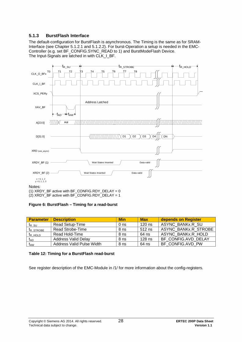
5.1.3 BurstFlash Interface The default-configuration for BurstFlash is asynchronous. The Timing is the same as for SRAM-Interface (see Chapter 5.1.2.1 and 5.1.2.2). For burst-Operation a setup is needed in the EMC-Controller (e.g. set BF_CONFIG.SYNC_READ to 1) and BurstModeFlash Device. The Input-Signals are latched in with CLK_I_BF.
CLK_I_BF
XCS_PERy
A[23:0]
D[31:0]
XRD (xoe_async)
XAV_BF
tR_SU tR_HOLD
XRDY_BF (1)
DN
Address Latched
Wait States Inserted
D1 D2 D3 D4
Adr
Data valid
x = 0, 1, 2y = 0, 1, 2, 3
tR_STROBE
tAD tAW
T0 T7T1 T2 T3 T4 T5 T6 T8CLK_O_BFx
Wait States Inserted Data validXRDY_BF (2)
Notes: (1) XRDY_BF active with BF_CONFIG.RDY_DELAY = 0 (2) XRDY_BF active with BF_CONFIG.RDY_DELAY = 1
Figure 6: BurstFlash – Timing for a read-burst
Parameter Description Min Max depends on Register tR_SU Read Setup-Time 0 ns 120 ns ASYNC_BANKx.R_SU tR_STROBE Read Strobe-Time 8 ns 512 ns ASYNC_BANKx.R_STROBE tR_HOLD Read Hold-Time 8 ns 64 ns ASYNC_BANKx.R_HOLD tAD Address Valid Delay 8 ns 128 ns BF_CONFIG.AVD_DELAY tAW Address Valid Pulse Width 8 ns 64 ns BF_CONFIG.AVD_PW
Table 12: Timing for a BurstFlash read-burst
See register description of the EMC-Module in /1/ for more information about the config-registers.
Copyright © Siemens AG 2014. All rights reserved. 29 ERTEC 200P Data Sheet Technical data subject to change. Version 1.1
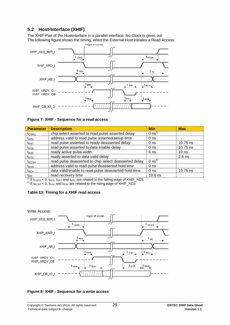
5.2 Host-Interface (XHIF) The XHIF-Part of the Hostinterface is a parallel interface. No Clock is given out. The following figure shows the timing, when the External Host initiates a Read Access.
Figure 7: XHIF - Sequence for a read access
Parameter Description Min Max tCSRS chip select asserted to read pulse asserted delay 0 ns1) tARS address valid to read pulse asserted setup time 0 ns tRRT read pulse asserted to ready deasserted delay 0 ns 10.75 ns tRDE read pulse asserted to data enable delay 0 ns 10.75 ns tRAP ready active pulse width 6 ns 10 ns tRTD ready asserted to data valid delay 2.6 ns tRCSH read pulse deasserted to chip select deasserted delay 0 ns2) tRAH address valid to read pulse deasserted hold time 0 ns tRDH data valid/enable to read pulse deasserted hold time 0 ns 10.75 ns tRR read recovery time 10.6 ns 1) If tCSRS < 0, tARS, tRRT and tRDE are related to the falling edge of XHIF_XCS 2) If tRCSH < 0, tRAH and tRDH are related to the rising edge of XHIF_XCS
Table 13: Timing for a XHIF read access
Write Access:
Figure 8: XHIF - Sequence for a write access
Copyright © Siemens AG 2014. All rights reserved. 30 ERTEC 200P Data Sheet Technical data subject to change. Version 1.1
Parameter Description Min Max tCSWS chip select asserted to write pulse asserted delay 0 ns1) tAWS address valid to write pulse asserted setup time 0 ns tWRT write pulse asserted to ready deasserted delay 0 ns 10.86 ns tWDE write pulse asserted to data enable setup 0 ns 3) tWDV write pulse asserted to data valid delay 13.4 ns tRAP ready active pulse width 6 ns 10 ns tWCSH write pulse deasserted to chip select deasserted delay 0 ns2) tWAH address valid to write pulse deasserted hold time 0 ns tRTW ready asserted to write pulse deasserted delay 0 ns tWDH data valid/enabled to read pulse deasserted hold time 0 ns2) tWR write recovery time 10.6 ns 1) If tCSWS < 0, tAWS, tWRT and tWDE are related to the falling edge of XHIF_XCS 2) If tWCSH < 0, tWAH and tWDH are related to the rising edge of XHIF_XCS 3) tWDE may get any value, as long as it is assured, that there is 1 idle cycle (of the XHIF clock period) guaranteed between the end of the preceding access and the start of the current access (indicated by the falling edge of XCS/XWR). Within this idle cycle no access is allowed at all.
Table 14: Timing for a XHIF write access
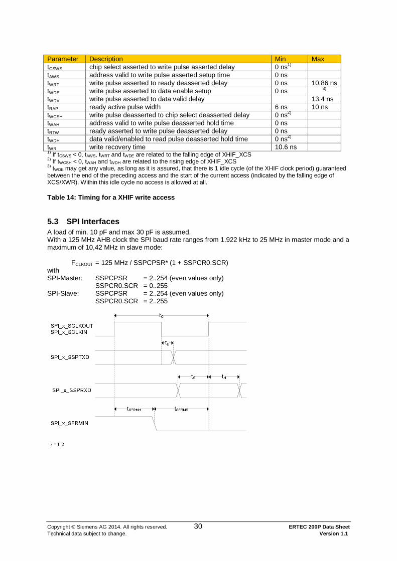
5.3 SPI Interfaces A load of min. 10 pF and max 30 pF is assumed. With a 125 MHz AHB clock the SPI baud rate ranges from 1.922 kHz to 25 MHz in master mode and a maximum of 10,42 MHz in slave mode: FCLKOUT = 125 MHz / SSPCPSR* (1 + SSPCR0.SCR) with SPI-Master: SSPCPSR = 2..254 (even values only)
SSPCR0.SCR = 0..255 SPI-Slave: SSPCPSR = 2..254 (even values only)
SSPCR0.SCR = 2..255

Copyright © Siemens AG 2014. All rights reserved. 31 ERTEC 200P Data Sheet Technical data subject to change. Version 1.1
Symbol Parameter Min. Max. Unit Note tC Baud rate 40
48 520000 ns Master mode
Slave mode tD Valid delay -3 3 ns 1)
tS Setup Time 9 ns 2)
tH Hold Time 0 ns 2)
tSFRMS SFRMIN Setup Time
8 ns
tSFRMH SFRMIN Hold Time 16 ns
1) Load capacitance = 30pF 2) Ts, Th > one 125 MHz period; inputs are synchronized with AHB Clock (FSSPCLK).
Table 15: Timing for a SPI access
To avoid damage caused by contention on the SPI outputs, serial resistors are recommended to reduce the maximum current.
5.4 PNPLL The nine output-signals PNPLL_out(8..0) can be routed to external Pins via GPIOs. The following parameterization in the PN-IP must be done therefore: - Register CycleCompare_A_1 = 0x0000_0000 (Trigger-Impuls on Cycle-start) - Register PLL_OUT_Control_0 = 0x0000_0016 (Event appears on Signal pn_pll_o(0)) On the ERTEC 200P Toplevel the multiplexers and GPIOs must be adapted accordingly. On the selected GPIO-Pin PNPLL_OUT can be measured. It is generated as follows:
t0: Cycle-start, i.e. point of time in which the Cycle-Timer breaks from a maximum value to its minimal value. t1: pn_pll_o is emitted from the PNIP t2: The signal PNPLL_OUT appears on the external GPIO-Pin In the PN-IP the following delay is generated:
Time Description Min/Max (ns) PN-IP t0 t1 Time from Cycle_A-break to change of the PN-IP internal Flip-
Flop pn_pll_o(0) from 1 to 0. 24ns (exactly three 8ns-Clocks)
ERTEC 200P t1 t2 Output_delay from one of the following PN-PLL-Outputs from PN-IP to GPIO-Pin.
see following table
Signal (Input) Ports
Alternate Function Input_delay Load (pF)
Min / Max -min -max
PNPLL_EXTIN_A GPIO_9 A 1.58ns 3.00ns - GPIO_23 B 1.52ns 2,77ns -
Signal Clock-to-Output_delay Cylce-start to Output delay
Copyright © Siemens AG 2014. All rights reserved. 32 ERTEC 200P Data Sheet Technical data subject to change. Version 1.1
(Output) (t1 -> t2) (t0 -> t2) -min -max -min -max
PNPLL_OUT0 GPIO_0 A 4,98ns 13,30ns 28,98ns 37,30ns 10 / 30 GPIO_56 C 4,34ns 11,04ns 28,34ns 35,04ns 10 / 30
PNPLL_OUT1 GPIO_1 A 5,02ns 12,76ns 29,02ns 36,76ns 10 / 30 GPIO_57 C 4,35ns 11,08ns 28,35ns 35,08ns 10 / 30
PNPLL_OUT2 GPIO_2 A 4,90ns 12,95ns 28,90ns 36,95ns 10 / 30 GPIO_58 C 4,35ns 10,91ns 28,35ns 34,91ns 10 / 30
PNPLL_OUT3 GPIO_3 A 4,93ns 12,30ns 28,93ns 36,30ns 10 / 30 GPIO_59 C 4,36ns 10,88ns 28,36ns 34,88ns 10 / 30
PNPLL_OUT4 GPIO_4 A 4,78ns 12,17ns 28,78ns 36,17ns 10 / 30 GPIO_60 C 4,30ns 11,78ns 28,30ns 35,78ns 10 / 30
PNPLL_OUT5 GPIO_5 A 4,85ns 12,09ns 28,85ns 36,09ns 10 / 30 GPIO_61 C 4,24ns 10,68ns 28,24ns 34,68ns 10 / 30
PNPLL_OUT6 GPIO_6 A 4,76ns 11,87ns 28,76ns 35,87ns 10 / 30 GPIO_29 C 4,32ns 10,88ns 28,32ns 34,88ns 10 / 30
PNPLL_OUT7 GPIO_7 A 4,47ns 11,08ns 28,47ns 35,08ns 10 / 30 GPIO_30 C 4,35ns 10,81ns 28,35ns 34,81ns 10 / 30
PNPLL_OUT8 GPIO_8 A 4,79ns 11,84ns 28,79ns 35,84ns 10 / 30 GPIO_31 C 4,34ns 10,81ns 28,34ns 30,81ns 10 / 30
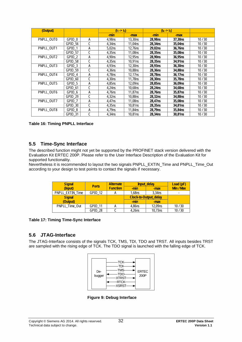
Table 16: Timing PNPLL Interface
5.5 Time-Sync Interface The described function might not yet be supported by the PROFINET stack version delivered with the Evaluation Kit ERTEC 200P. Please refer to the User Interface Description of the Evaluation Kit for supported functionality. Nevertheless it is recommended to layout the two signals PNPLL_EXTIN_Time and PNPLL_Time_Out according to your design to test points to contact the signals if necessary.
Signal (Input) Ports Alternate
Function Input_delay Load (pF)
Min / Max -min -max PNPLL_EXTIN_Time GPIO_12 A 1,68ns 3,34ns -
Signal (Output) Clock-to-Output_delay -min -max
PNPLL_Time_Out GPIO_11 A 4,86ns 12,09ns 10 / 30 GPIO_28 C 4,26ns 10,73ns 10 / 30
Table 17: Timing Time-Sync Interface
5.6 JTAG-Interface The JTAG-Interface consists of the signals TCK, TMS, TDI, TDO and TRST. All inputs besides TRST are sampled with the rising edge of TCK. The TDO signal is launched with the falling edge of TCK.
De-bugger
ERTEC200P
TCKTDI
TDOTMS
XTRSTRTCK
XSRST
Figure 9: Debug Interface
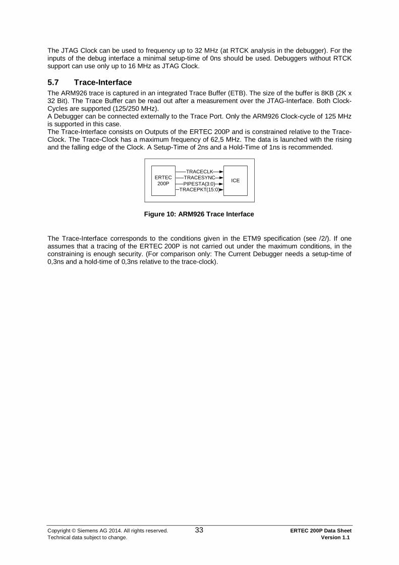
Copyright © Siemens AG 2014. All rights reserved. 33 ERTEC 200P Data Sheet Technical data subject to change. Version 1.1
The JTAG Clock can be used to frequency up to 32 MHz (at RTCK analysis in the debugger). For the inputs of the debug interface a minimal setup-time of 0ns should be used. Debuggers without RTCK support can use only up to 16 MHz as JTAG Clock.
5.7 Trace-Interface The ARM926 trace is captured in an integrated Trace Buffer (ETB). The size of the buffer is 8KB (2K x 32 Bit). The Trace Buffer can be read out after a measurement over the JTAG-Interface. Both Clock-Cycles are supported (125/250 MHz). A Debugger can be connected externally to the Trace Port. Only the ARM926 Clock-cycle of 125 MHz is supported in this case. The Trace-Interface consists on Outputs of the ERTEC 200P and is constrained relative to the Trace-Clock. The Trace-Clock has a maximum frequency of 62,5 MHz. The data is launched with the rising and the falling edge of the Clock. A Setup-Time of 2ns and a Hold-Time of 1ns is recommended.
ERTEC200P ICE
TRACECLKTRACESYNC
TRACEPKT(15:0)PIPESTA(3:0)
Figure 10: ARM926 Trace Interface
The Trace-Interface corresponds to the conditions given in the ETM9 specification (see /2/). If one assumes that a tracing of the ERTEC 200P is not carried out under the maximum conditions, in the constraining is enough security. (For comparison only: The Current Debugger needs a setup-time of 0,3ns and a hold-time of 0,3ns relative to the trace-clock).
Copyright © Siemens AG 2014. All rights reserved. 34 ERTEC 200P Data Sheet Technical data subject to change. Version 1.1
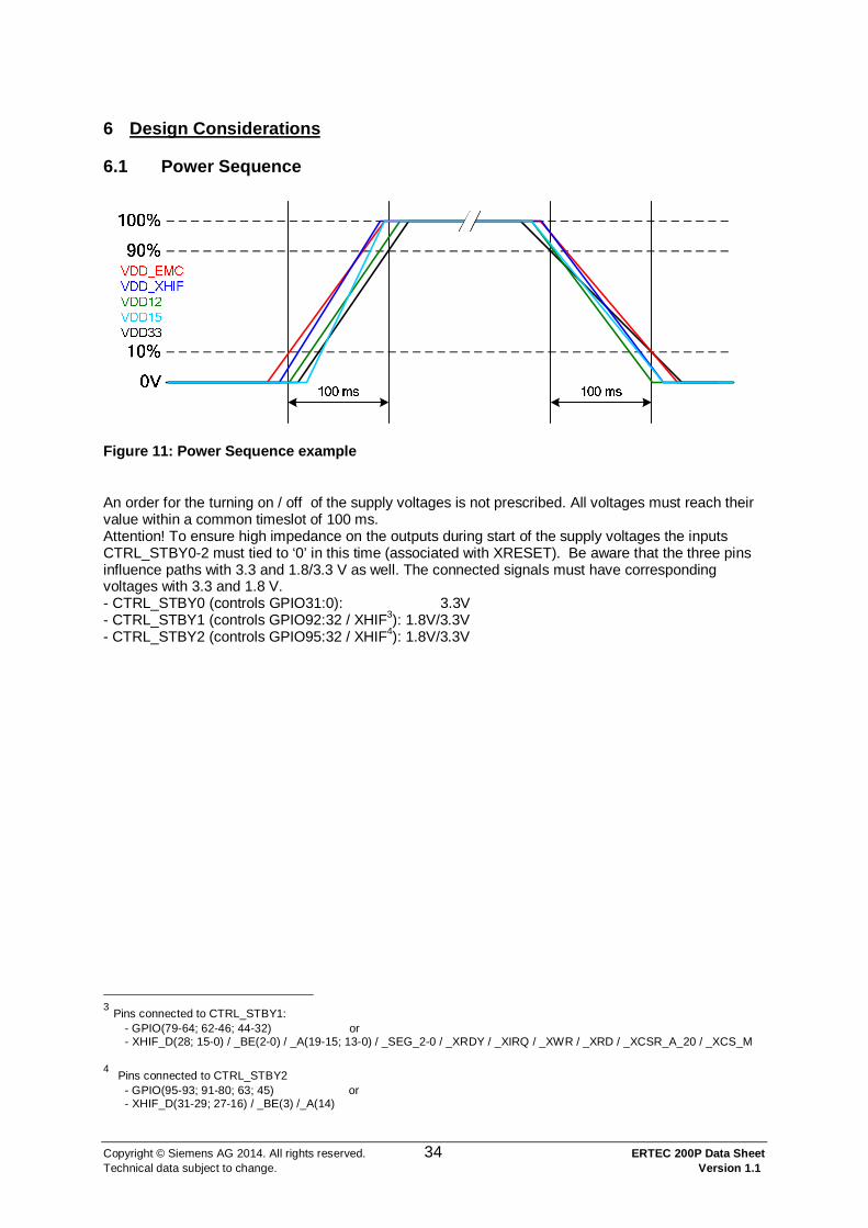
6 Design Considerations
6.1 Power Sequence
Figure 11: Power Sequence example
An order for the turning on / off of the supply voltages is not prescribed. All voltages must reach their value within a common timeslot of 100 ms. Attention! To ensure high impedance on the outputs during start of the supply voltages the inputs CTRL_STBY0-2 must tied to ‘0’ in this time (associated with XRESET). Be aware that the three pins influence paths with 3.3 and 1.8/3.3 V as well. The connected signals must have corresponding voltages with 3.3 and 1.8 V. - CTRL_STBY0 (controls GPIO31:0): 3.3V - CTRL_STBY1 (controls GPIO92:32 / XHIF3): 1.8V/3.3V - CTRL_STBY2 (controls GPIO95:32 / XHIF4): 1.8V/3.3V
3 Pins connected to CTRL_STBY1:
- GPIO(79-64; 62-46; 44-32) or - XHIF_D(28; 15-0) / _BE(2-0) / _A(19-15; 13-0) / _SEG_2-0 / _XRDY / _XIRQ / _XWR / _XRD / _XCSR_A_20 / _XCS_M
4 Pins connected to CTRL_STBY2
- GPIO(95-93; 91-80; 63; 45) or - XHIF_D(31-29; 27-16) / _BE(3) /_A(14)
Copyright © Siemens AG 2014. All rights reserved. 35 ERTEC 200P Data Sheet Technical data subject to change. Version 1.1
6.2 ERTEC 200P Design recommendations
6.2.1 Design recommendations for ERTEC 200P EMC Bus
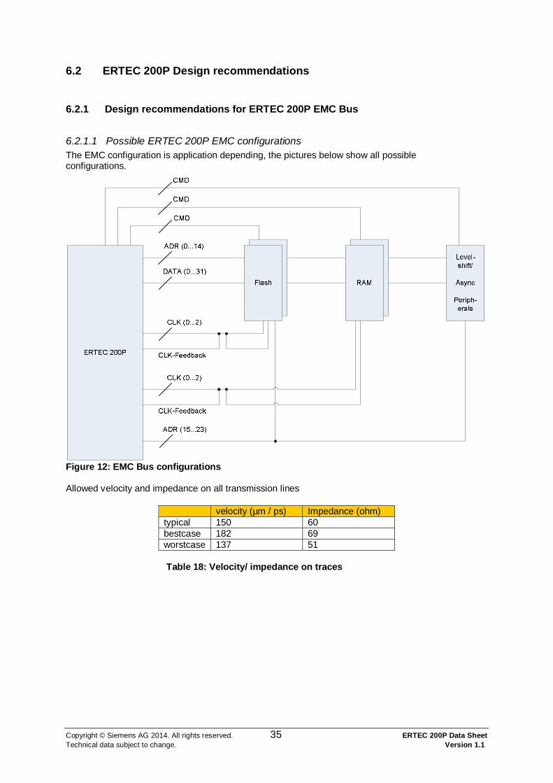
6.2.1.1 Possible ERTEC 200P EMC configurations The EMC configuration is application depending, the pictures below show all possible configurations.
Figure 12: EMC Bus configurations Allowed velocity and impedance on all transmission lines
velocity (µm / ps) Impedance (ohm) typical 150 60 bestcase 182 69 worstcase 137 51
Table 18: Velocity/ impedance on traces

Copyright © Siemens AG 2014. All rights reserved. 36 ERTEC 200P Data Sheet Technical data subject to change. Version 1.1
6.2.1.2 ERTEC 200P EMC recommendations The recommended values below full fill all these bus configurations/ requirements for ERTEC 200P:
Min/Max length configuration from driver to receiver
Max length [mm]
Min length [mm]
Max Vias
Adress [0-14] 87 6 5 Adress [15-23]/ CMD 84 6 4 Data 114 17 4 Clock/ CMD-DQMs 80 17 2
Table 19: Min/ max trace length
All transmission lines should be routed on inner layers and referenced to Ground. All Clocks to SD-RAM and the associated feedback clock to ERTEC 200P must be length
matched within 1mm. All Clocks to Flash and the associated feedback clock to ERTEC 200P must be length
matched within 1mm. Clocks must always be routet as short as possible. Length matching between Data and Adress to their corresponding clocks is not necessary. Clock must be shorter as shortest Data line. If Address is below 17mm, clock max length is 17mm (corner case).
Usecase “External Host”

Copyright © Siemens AG 2014. All rights reserved. 37 ERTEC 200P Data Sheet Technical data subject to change. Version 1.1
In the case where just one participant is on ADR (address), Data or CMD/CTR line (see above) an additional 8,2pF capacitor is necessary on SDRAM signal lines (take care on dedicated SDRAM signals).
6.2.1.3 Controlling of an external Level-Shifter The external Level-Shifter can be controlled by the signals DTXR and XOE_DRIVER on the EMC-Interface. The signals can only be used for the asynchronous memories. The usage of the signals is optional. The control signals (DTXR and XOE_DRIVER) for the Level-Shifter will be activated independent of the respective address area of the asynchronous EMC-Interface (CS0-CS3) and not particular to the chip select. At accesses to a memory before or after the Level-Shifter the memories at both sides of the Level-Shifter will be active. This leads to the situation that two participants drive the data bus of the EMC. To prevent this situation an appropriate logic (marked in blue) has to be integrated, see figure bellow.
Note: It is necessary to use appropriate pull resistors, signed in green, because the signals DTXR and XOE_DRIVER will be latched at reset for the boot information.
6.2.2 Design Recommendations ERTEC 200P supply voltages pins see also Chapter 2.2
6.2.3 Design Recommendations for ERTEC 200P Profinet PHYs 6.2.3.1 ERTEC 200P PHY supply voltages pins see also Chapter 2.2

Copyright © Siemens AG 2014. All rights reserved. 38 ERTEC 200P Data Sheet Technical data subject to change. Version 1.1
6.2.3.2 Filtering on ERTEC 200P PHY supply voltages It is recommended to use one power filters (PI-Filters) for VDD33ESD, VDDACB and an additional one for PxVDDARXTX, VDDAPLL. The GND pins PVSSA and VSSAPLLCB should also be separated by a power filter or connected to digital ground at far end from ERTEC 200P.
PxVDDARXTX
VDDACB
VDD15
VDDAPLL
PVSSA
VDDQ(PECL)x
VDD33ESD
VSSAPLLCB
DVDDy
DGNDy
GNDGND
1.5V 3.3V 3.3V 1.5V
DGND
AGND
3.3V_Analog
1.5V_Analog
Note: x = 1,2; y = 1,3 Figure 13: PHY power filtering
Recommended PI-Power filter:

Copyright © Siemens AG 2014. All rights reserved. 39 ERTEC 200P Data Sheet Technical data subject to change. Version 1.1
VDD_Analog
AGNDGND
Ferrite Bead 150Ohm @ 100Mhz
Ceramic Capacitors are +-20%
100nF
VDD
100nF
BLM15
Figure 14: PI Filter
6.2.3.3 Decoupling on ERTEC 200P PHY supply voltages It is recommend to use three types of decoupling capacitors as shown. The red pair of 10nF and 22nF should be placed as close as possible to DVDD1, DVDD3, VDD33ESD, VDDACB, P1VDDARXTX, P2VDDARXTX and VDDAPLL. The orange pair of 100nF and 22uF should be placed once to the net for DVDD1/3, VDDESD/VDDACB and P1VDDARXTX/ P2VDDARXTX/ VDDAPLL. The blue 100nF capacitor (shown in blue) should be placed as close as possible for all remaining pins VDD15 and VDDQ(PECL)1/2 to the pins.
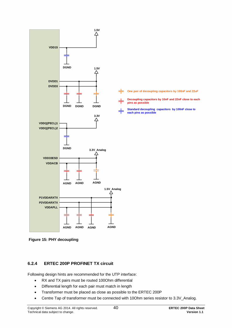
Copyright © Siemens AG 2014. All rights reserved. 40 ERTEC 200P Data Sheet Technical data subject to change. Version 1.1
P2VDDARXTX
VDDACB
VDD15
VDDAPLL
VDDQ(PECL)1
VDD33ESD
DVDD1
1.5V
3.3V
DGND
AGND
1.5V_Analog
3.3V_Analog
DVDD3
1.5V
DGND DGND
One pair of decoupling capacitors by 100nF and 22uF
Decoupling capacitors by 10nF and 22nF close to each pins as possible
VDDQ(PECL)2
AGND AGNDAGND
P1VDDARXTX
AGNDAGNDAGND
Standard decoupling capacitors by 100nF close to each pins as possible
DGND
DGND
Figure 15: PHY decoupling
6.2.4 ERTEC 200P PROFINET TX circuit Following design hints are recommended for the UTP interface:
RX and TX pairs must be routed 100Ohm differential Differential length for each pair must match in length Transformer must be placed as close as possible to the ERTEC 200P Centre Tap of transformer must be connected with 10Ohm series resistor to 3.3V_Analog.

Copyright © Siemens AG 2014. All rights reserved. 41 ERTEC 200P Data Sheet Technical data subject to change. Version 1.1
50Ohm termination resistors must be placed as close as possible to the ERTEC 200P An external 12.4kOhm pull down resistor on pin EXTRES must be placed a close as possible to
ERTEC 200P Analog signals must be placed referenced to analog ground plane or common plane (same as
digital) and must be not coupled with other signals. The picture below shows a typical UTP circuit with separate centre taps on the magnetic:
10R
10nF
AGND
50R 50R
10R
10nF
AGND
50R 50R
12.4K
AGND
75R 50R
75R
50R
50R
50R
50R
50R
Case/ Shield
1M
1M
4.7nF2KV
GND GND
1:1
1:1
Figure 16: UTP circuit
Note: UTP interface must full fill ANSI X3.263-1995 FDDI specifications.
6.2.4.1 ERTEC 200P PROFINET TX circuit unused pins Unused UTP port should be left open, but EXTRES must be connected as recommended.

Copyright © Siemens AG 2014. All rights reserved. 42 ERTEC 200P Data Sheet Technical data subject to change. Version 1.1
Figure 17: UTP circuit unused
6.2.5 ERTEC 200P PROFINET FX circuit Following design hints are recommended for the FX interface:
It is strongly recommended to use PROFINET compliant POF Transceiver QFBR-5978AZ from company Avago.
RX and TX pairs (LVPECL) must be routed 100Ohm differential Differential length for each pair must match in length Transceiver must be placed as close as possible to the ERTEC 200P 150Ohm series resistors in TX path must be placed as close as possible to the ERTEC 200P The RX termination (130Ohm pull up and 82Ohm pull down) must be placed a close as
possible to ERTEC 200P RX and TX Power supply on transceiver should separately filtered, see datasheet transceiver. Care must be taken on level translation between transceiver SD pin and ERTEC 200P PHY
input, see recommended circuit below. Signals must be placed referenced to digital ground plane or common plane and must be not
coupled with other signals. Don’t connect analog VDD/ AGND (related pins on ERTEC 200P: VDD33ESD, VDDACB/
PVSSA, VSSPLLCB) to FX circuit.

Copyright © Siemens AG 2014. All rights reserved. 43 ERTEC 200P Data Sheet Technical data subject to change. Version 1.1
The picture below shows the recommended FX circuit:
10K
GND
130R
150R
150R
130R
82R 82R
GND
4k7 4k7
Level translation
Use GPIO(4), GPIO(5) for port 1 and GPIO(6), GPIO(7) for port 2!
Place near PHY/ ERTEC 200P!
Figure 18: FX circuit
6.2.5.1 ERTEC 200P/ Avago QFBR-5978AZ SD circuit The Avago QFBR-5978AZ has a single ended output and ERTEC 200P has a differential LVPECL input, following level translation circuit is recommended. Comparator should be placed near transceiver and PECL driver near ERTEC 200P. The 3,3V supply voltage tolerance for POF transceiver and SD level translation circuit is limited to +- 5%.

Copyright © Siemens AG 2014. All rights reserved. 44 ERTEC 200P Data Sheet Technical data subject to change. Version 1.1
Figure 19: SD level translation circuit
6.2.5.2 ERTEC 200P PROFINET FX circuit unused pins PxTDXP/N Signals on unused FX port should be left open, PxRDXP/N and PxSDXP/N inputs should directly connected to GND, the GPIOs could used for alternate function.
Figure 20: FX circuit unused pins
Copyright © Siemens AG 2014. All rights reserved. 45 ERTEC 200P Data Sheet Technical data subject to change. Version 1.1
6.3 Clocking
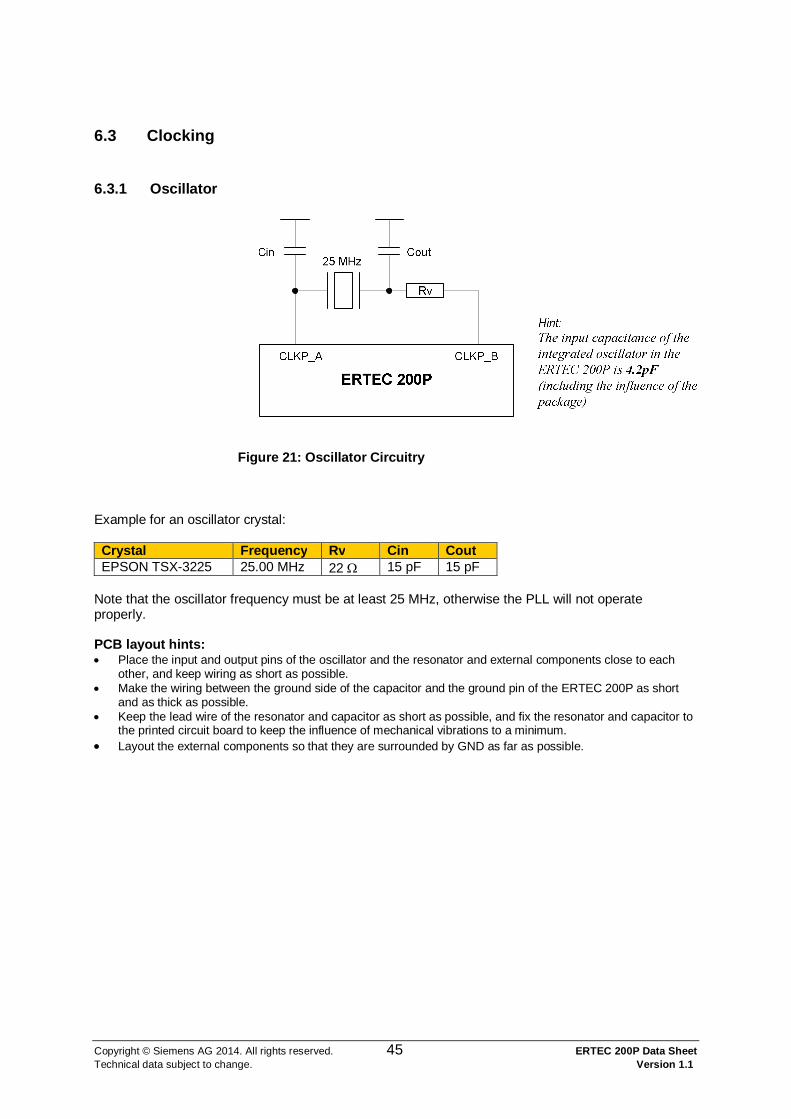
6.3.1 Oscillator
Figure 21: Oscillator Circuitry
Example for an oscillator crystal: Crystal Frequency Rv Cin Cout EPSON TSX-3225 25.00 MHz 22 15 pF 15 pF
Note that the oscillator frequency must be at least 25 MHz, otherwise the PLL will not operate properly. PCB layout hints: Place the input and output pins of the oscillator and the resonator and external components close to each
other, and keep wiring as short as possible. Make the wiring between the ground side of the capacitor and the ground pin of the ERTEC 200P as short
and as thick as possible. Keep the lead wire of the resonator and capacitor as short as possible, and fix the resonator and capacitor to
the printed circuit board to keep the influence of mechanical vibrations to a minimum. Layout the external components so that they are surrounded by GND as far as possible.
Copyright © Siemens AG 2014. All rights reserved. 46 ERTEC 200P Data Sheet Technical data subject to change. Version 1.1
Figure 22 : Oscillator Circuitry Layout Example
6.3.2 External clock source It is possible to use an external clock source instead of a quartz crystal as clock input for port CLKP_A as well. In this case the Port CLKP_B has to be left unconnected (open) and the port CLKP_A has to fulfill the following requirements: Parameter Description Min Typ Max Unit fIN external clock source frequency 1) 25 1) MHz VIH CLKP_A high level voltage 2 3,3 VDDACB V VIL CLKP_A low level voltage 0 - 0,8 V tRFC CLKP_A rise or fall time 0 1 4 ns tw CLKP_A high or low time 16 2) 20 2) 24 2) ns tJIT CLKP_A jitter tolerace - 20 - ps
(RMS) DuCy CLKP_A duty cycle 40 50 60 % 1) +/- 50ppm over the whole lifetime and temperature range 2) tw was calculated at fIN(TYP) = 25MHz , e.g. tw(MIN) = 10* (DuCy(MIN) / fIN(TYP))
6.3.3 PLL Power Supply Since GND noise may affect VDD through C1 and C2, GND must be stable.

Copyright © Siemens AG 2014. All rights reserved. 47 ERTEC 200P Data Sheet Technical data subject to change. Version 1.1
AVDD
AGND
C1C2
VDD
GND
LR
Figure 23: Recommended for PLL Power Supply Filter
Dimensioning the PLL Power Supply Filter
factor) damping(2
21
LCCRR L
Hz)in frequency off(cut )(2
1
210 CCL
f
where R+RL 0.8 , C2 10 µF, 0.7 (should not be less than 0.7 to decrease the sensitivity for resonance), f0 <= 5kHz Example: With R+RL = 0.8 , L = 22 µH, C2 = 68 µF, C1 = 0.3 µF (ceramic capacitor) this results in f0 = 4.1 kHz and = 0.70. C1 should be an SMD capacitor (e.g. ceramic 300 nF) for elimination of high frequency components. Be sure to place it as close as possible to a power supply pin.

Copyright © Siemens AG 2014. All rights reserved. 48 ERTEC 200P Data Sheet Technical data subject to change. Version 1.1
6.4 Reset The minimal duration for reset is shown in the table below. Parameter Symbol Min Typ Max Unit Reset pulse width 1) tRES1 30 µs Reset pulse width 2) tRES2 40 ns 1) Applies to pin XRESET during power-up phase (accounts for oscillator start-up time) 2) Applies to pins XSRST and XTRST for operating, powered-up ASIC (oscillator is running)
Table 20: Minimal reset duration
6.4.1 Power-On Reset Behaviour
V D D
S TB Y (PLL )
C LK P _A
m in. 30us
U ns tab le m in . 1us
X R E S E T
m in . 2 ,5us
Figure 24: Power-On Reset Behaviour

Copyright © Siemens AG 2014. All rights reserved. 49 ERTEC 200P Data Sheet Technical data subject to change. Version 1.1
Figure 25: Timing reset
On access, e.g. over the XHIF-Interface, to internal resources of the ERTEC 200P directly after release of XRESET is to mention, that they are only allowed after the internal initialisation is finished (see also StartUp-Times in Chapter 7.7.1) Duration of initialisation after deactivating the XRESET: PLL-Standby-Time: 32,5 µs PLL-Lockup-Time: 1002,5 µs EMC Init_Done 1): 233,0 µs Complete-Time: 1268,0 µs 1) Parallel to the EMC Init_Done several internal SRAMs are also initialised in this time. The time for the EMC Init_Done is the biggest. Therefore it is listed here.
6.4.2 Strapping Pins During XRESET is active, the Input-Value for the Config- and Boot-Pins are LATCHED in. After XRESET is released, the values are stored. The values on the Config- and Boot-Pins must stay stable 120ns after the XRESET is released. See Chapter 7.6 and 7.7 for more details
6.4.3 Reset Structure

Copyright © Siemens AG 2014. All rights reserved. 50 ERTEC 200P Data Sheet Technical data subject to change. Version 1.1
6.4.3.1 Asynchronous PowerOn-Reset The asynchronous5 PowerOn-Reset is connected via the Pin XRESET to the ERTEC 200P. As reaction to this reset the complete circuit (incl. Clock-system) of the ERTEC 200P is reset and the Configuration- and Boot-Pins are latched (see Chapter 0). The PowerOn-Reset must stay active for at least 30 µs after the supply-voltages are supplied. Afterwards the PLL ramps up and is locked 1000µs later. The time until lock of the PLL is called tLOCK. The PowerOn-Reset-Phase is internally enlarged for this time (PLL-Lock is not interpreted) and the Clock-system is connected at the end of the rampup-phase. The internal reset stays active for additional 16 Clocks to reset the internal logic. A communication of the debugger over the JTAG-interface is not possible at this time.
f/MHz
t/µs
tLOCK = 1000µs
30
Startup PLLactiveReset
500
Figure 26: StartUp of the PLL
The lock-state of the PLL is monitored by a hardware. The IRQ49 interrupt announces whether the PLL has lost its input clock (quartz break) or the PLL is not locked (PLL-Monitor, monitors input- to output-frequency). Additionally the two Error-states can be polled from the SCRB-Register ‘PLL_STAT_REG’. An integrated filter of the ERTEC 200P ensures that spikes <= 40ns (bestcase) on the input XRESET are eliminated. In order to analyse the Reset-Source after a restart, the Bit PWRON_HW_RES of the Register RES_STAT_REG is set on PowerOn-Reset. On restart the software can read the Register RES_STAT_REG.
6.4.3.2 Asynchronous Hardware-Reset The hardware-reset is activated over the Pin XSRST from an external debugger. XSRST is a bidirectional IO-cell with Open-Drain output. During the active XSRST-Phase the complete internal logic is reset, but not the Clock-system. Additionally the configuration-pins are not latched. During the Hardware-Reset-Phase the debugger can communicate over the JTAG-Interface with the embedded ICE Logic, e.g. to load a breakpoint. Thereby a single-stepping from the reset-address is possible. An integrated filter of the ERTEC 200P ensures that spikes <= 40ns (bestcase) on the input XSRST are eliminated. In order to analyse the Reset-Source after a restart, the Bit PWRON_HW_RES of the Register RES_STAT_REG is set on PowerOn-Reset. On restart the software can read the Register RES_STAT_REG. On Reboot after a hardware-reset the system uses the bootmode which was latched during the PowerOn-Reset. XSRST is activated to the debugger if PowerOn-Reset is active It is forbidden to activate XSRST during a ‘RES_SOFT_ARM926_CORE’ is active! The Debugger won’t run during if the core is in reset.
6.4.3.3 Asynchronous JTAG-Reset The JTAG-Reset is activated through the Pin XTRST from the external debugger. Only the embedded ICE logic of the ARM926EJ-S is reset. To ensure a defined state of the embedded ICE logic without using a debugger, the logic is also resetted during PowerOn-Reset (XRESET). An integrated filter of the ERTEC 200P ensures that spikes <= 40ns (bestcase) on the input XTSRST are eliminated. Normally a spike on XTRST is not passed to the JTAG Controler. A sequence is therefore necessary on TDI/TMS and TCK.
5 The asynchronous Reset acts on the Reset-Input of a Flip-Flop. The Reset is assigned asynchronous but released synchronous.

Copyright © Siemens AG 2014. All rights reserved. 51 ERTEC 200P Data Sheet Technical data subject to change. Version 1.1
Hint for board-layout: Instructions for external Pull-Resistors on XTRST can be found in Chapter 2.1.4
6.4.3.4 Asynchronous ARM926 Watchdog-Reset The ARM926 Watchdog-Reset forms a hardware observation of the software from the ARM926EJ-S. The base for the observation is a time which is adjustable in the watchdog-timer. On activation of the watchdog the time counts. If no retrigger is done within this time, the watchdog-reset (XRES_ARM926_WD) is triggered (output ARM926 watchdog: WD_XWDOUT1). If the watchdog-function is enabled (WD_RES_FREI_ARM926) the ERTEC 200P is reset. In order to analyse the Reset-Source after a restart, the Bit ARM926_WDOG_RES of the Register RES_STAT_REG is set on PowerOn-Reset. The Bit keeps set from the reset-function. On restart the software can read the Register RES_STAT_REG. For application, in which the expiration of the watchdog should have no negative effect on the PN-IP, the PN-IP can be excluded from the reset per watchdog (EN_WD_RES_PN = 0 in ASYN_RES_CTRL_REG). Attention: The Bit EN_WD_RES_PN is always set if the PN-IP is reset! If an asynchronous software-reset is generated from the software for the PN-IP, the software has to set EN_WD_RES_PN = 0 if the Watchdog-Reset of the ARM926 should have no effect to the PN-IP. In advance to the watchdog expiration an interrupt ‘WD_INT_ARM926’ is generated to the ARM926 and to an external host the watchdog expiration is advanced with ‘WD_XWDOUT0’ over a GPIO-Pin. The watchdog also expires if the clock-generation fails (e.g. quartz break). The PLL enters his free-running-frequency in this case (100 – 300 MHz). On Reboot after a Watchdog-Reset the system uses the bootmode which was latched during the PowerOn-Reset.
6.4.3.5 Asynchronous Software-Reset for the ERTEC 200P (without PN-IP) In the ERTEC 200P an asynchronous Software-Reset can be generated by setting the Bit ‚RES_SOFT’ in the Register RES_CTRL_REG. The PN-IP and the PHYs are not reset in this case. In order to analyse the Reset-Source after a restart, the Bit SW_RES of the Register RES_STAT_REG is set on Software-Reset. The Bit keeps set from the reset-function. On restart the software can read the Register RES_STAT_REG. On Reboot after a hardware-reset the system uses the bootmode which was latched during the PowerOn-Reset.
6.4.3.6 Asynchronous Software-Reset of the PN-IP The PN-IP and the PHYs can be reset separately from Software by setting the Bit ‘RES_SOFT_PN’ in the SCRB-Register ‘ASYN_RES_CTRL_REG’. The HW-Reset for the integrated PHYs comes from ‘phy_reset_o’ output of the PN-IP. If the SMI-Modul of the PN-IP is not active (configuration-mode) the ‘phy_reset_o’ output is active and keeps the PHYs in reset-state. A simultaneous SW-Reset for the ERTEC 200P and the PN-IP reset the complete ERTEC 200P.
6.4.3.7 Asynchronous Software-Reset of the ARM926EJ-S Core The ARM926EJ-S Core (without TCM926) has its own reset, which can be generated by setting the Bit ‚RES_SOFT_ARM926_CORE’ in the SCRB-Register ‘ASCN_RES_CTRL_REG’. ‘RES_SOFT_ARM926_CORE’ acts only to the ARM926EJ-S Core System and not to the TCM_Block_926. The TCM_Block_926 is reset with XRESET, XSRST, XRES_ARM926_WD or RES_SOFT. In order to analyse the Reset-Source after a restart, the Bit SW_RES_ARM926 of the Register RES_STAT_REG is set on Software-Reset. The Bit keeps set from the reset-function. On restart the software can read the Register RES_STAT_REG. The asynchronous Software-Reset for the ARM926EJ-S Core is necessary after the Bootloader has adjusted the final TCM926 configuration. Only with reset the ARM926EJ-S uses the TCM926 configuration (DRSIZE for D-TCM and IRSIZE for I-TCM configured in Register TCM926_MAP).
6.4.3.8 Synchronous Software-Reset (PN-IP, PER-IF, Hostinterface) The PN-IP, the Peripherie-Interface or the Host-Interface can also be reset from Software in the SCRB-Register ‚SYN_RES_CTRL_REG’ synchronously. This synchronous resets work on the SYN-

Copyright © Siemens AG 2014. All rights reserved. 52 ERTEC 200P Data Sheet Technical data subject to change. Version 1.1
Reset Inputs of the corresponding IPs and resets only the State-Machines and local registers, but not the parameterization-Registers and the AHB-Interface. The SW has to set the corresponding Bits in the Register ‘SYN_RES_CTRL_REG’ and reset them afterwards. With this function the software can control on it own the reset-state of the modules (short impulse: dyn. reset, constant ‘1’: disable-state).

Copyright © Siemens AG 2014. All rights reserved. 53 ERTEC 200P Data Sheet Technical data subject to change. Version 1.1
6.5 GPIO Pins The GPIO layer mainly provides means for flexible I/O pin mapping / routing. By use of multiplexers it is possible to obtain variable interconnections between predefined signal groups and ASIC I/O pins.
The structure of a single GPIO cell is shown below in Figure 27. Each cell can either be used for I/O pin routing or as input / output pin of the GPIO parallel ports.
AltFunction Out Output Enable
ASIC Logical ModulesAltFunction
In
Register PORTxOUT Register PORTxIN Register PORTxDIR
Register PORTxALTSEL0
Register PORTxALTSEL1
0 1 2 3M U X
0 1 2 3M U X
Single GPIO Cell (Port x Bit y)
withx = {0..1}y = {0..31} for Port 0y = {0..15} for Port 1
GPIO_Single.wmf
PAD
PORTx_y
0 1 2 3De-M U X
Figure 27: Single GPIO Cell
For I/O pin routing, one of 3 alternative functions can be selected for each GPIO cell (see Chapter 7.5 for GPIO pin mapping).
6.6 Pull-Up / Pull-Down Resistors The Renesas’ specifications for pull-up and pull-down resistors are listed in the table below. Resistor Type Min Typ Max Unit 50 k pull-up (3.3 V buffer) 40.5 51.9 70.1 k 50 k pull-up (1.8 V buffer) 38.6 49.7 66.9 k 50 k pull-down (3.3 V buffer) 37.0 49.6 70.4 k 50 k pull-down (1.8 V buffer) 35.8 47.6 66.4 k
Table 21: Pull-Up / Pull-Down Resistor Values
Since the maximum values of the internal pull-ups / pull-downs can be rather high in worst case, critical inputs (resets etc.) must not rely on the internal resistors but must be supplied with external pull-up / pull-down resistors. When combining external pull-up resistors with internal pull-down resistors (and vice versa) the following recommendation should be considered: A 50k internal pull-up (at its minimum value) combined with a 4k7pull-down results in a maximum
logic low level VIL of 0.36 V (VDD = 3.5 V, required: VIL 0.8 V).

Copyright © Siemens AG 2014. All rights reserved. 54 ERTEC 200P Data Sheet Technical data subject to change. Version 1.1
A 50k internal pull-down (at its minimum value) combined with a 10k pull-up results in a minimum logic high level VIL of 2.36 V (VDD = 3.0 V, required: VIH 2.0 V).
As a rule of thumb the values of the external resistors should not be higher than those listed above. Note that external components connected to a GPIO pin may have other switching thresholds and additional pull-up resistors which will reduce the effective pull-up resistor value on that GPIO pin.
6.7 Debug The debugging with the JTAG-Interface is described in /1/
7 Basic Configuration
7.1 Address Map A description can be found in /1/
7.2 Interrupts A description can be found in /1/
7.3 DMA Requests A description can be found in /1/
7.4 Timers A description can be found in /1/
7.5 GPIO Pin Mapping
GPIO Pin GPIO Registers
GPIO Alternative Function A
GPIO Alternative Function B
GPIO Alternative Function C
GPIO0_INT GPIO_*_0.0 PNPLL_OUT0_a TIM_OUT0_a NOT_USED GPIO1_INT GPIO_*_0.1 PNPLL_OUT1_a TIM_OUT1_a NOT_USED GPIO2_INT GPIO_*_0.2 PNPLL_OUT2_a TIM_OUT2 DBGRQ GPIO3_INT GPIO_*_0.3 PNPLL_OUT3_a TIM_OUT3 DBGACK GPIO4_INT GPIO_*_0.4 PNPLL_OUT4_a TIM_OUT4 I2C_SDOI_1_a GPIO5_INT GPIO_*_0.5 PNPLL_OUT5_a TIM_OUT5 I2C_SCLK_1_a GPIO6_INT GPIO_*_0.6 PNPLL_OUT6_a TIM_TRIG0_a I2C_SDOI_2_a GPIO7_INT GPIO_*_0.7 PNPLL_OUT7_a TIM_TRIG1_a I2C_SCLK_2_a GPIO8_INT GPIO_*_0.8 PNPLL_OUT8_a TIM_TRIG2 SPI_2_SCLKIN_b GPIO9_INT GPIO_*_0.9 PNCLKA_IN_a TIM_TRIG3 SPI_2_SFRMIN_b GPIO10_INT GPIO_*_0.10 NOT_USED TIM_TRIG4 SPI_2_SSPOE_b GPIO11_INT GPIO_*_0.11 PNTIME_OUT_a TIM_TRIG5 SPI_2_SSPCTLOE_b GPIO12_INT GPIO_*_0.12 PNTIME_IN U2_CTS SPI_2_SCLKOUT_b GPIO13_INT GPIO_*_0.13 WD_XWDOUT0_a U2_RTS SPI_2_SFRMOUT_b GPIO14_INT GPIO_*_0.14 I2C_SCLK_3 U2_TXD SPI_2_SSPTXD_b GPIO15_INT GPIO_*_0.15 I2C_SDOI_3 U2_RXD SPI_2_SSPRXD_b GPIO16 GPIO_*_0.16 SPI_1_SCLKOUT_a NOT_USED NOT_USED GPIO17 GPIO_*_0.17 SPI_1_SFRMOUT_a NOT_USED NOT_USED GPIO18 GPIO_*_0.18 SPI_1_SSPTXD_a NOT_USED NOT_USED GPIO19 GPIO_*_0.19 SPI_1_SSPRXD_a NOT_USED NOT_USED GPIO20 GPIO_*_0.20 SPI_1_SSPOE_a NOT_USED NOT_USED GPIO21 GPIO_*_0.21 SPI_1_SSPCTLOE_a NOT_USED NOT_USED GPIO22 GPIO_*_0.22 SPI_1_SFRMIN_a NOT_USED NOT_USED GPIO23 GPIO_*_0.23 SPI_1_SCLKIN_a PNCLKA_IN_b NOT_USED GPIO24 GPIO_*_0.24 SPI_2_SCLKOUT_a TIM_OUT0_b NOT_USED GPIO25 GPIO_*_0.25 SPI_2_SFRMOUT_a TIM_OUT1_b NOT_USED GPIO26 GPIO_*_0.26 SPI_2_SSPTXD_a TIM_TRIG0_b NOT_USED GPIO27 GPIO_*_0.27 SPI_2_SSPRXD_a TIM_TRIG1_b NOT_USED GPIO28 GPIO_*_0.28 SPI_2_SCLKIN_a U3_TXD PNTIME_OUT_b GPIO29 GPIO_*_0.29 SPI_2_SFRMIN_a U3_RXD PNPLL_OUT6_b GPIO30 GPIO_*_0.30 SPI_2_SSPOE_a NOT_USED PNPLL_OUT7_b GPIO31 GPIO_*_0.31 SPI_2_SSPCTLOE_a NOT_USED PNPLL_OUT8_b
Table 22: GPIO Port 0 Input Mapping

Copyright © Siemens AG 2014. All rights reserved. 55 ERTEC 200P Data Sheet Technical data subject to change. Version 1.1
GPIO Pin GPIO Registers
GPIO Alternative Function A
GPIO Alternative Function B
GPIO Alternative Function C
XHIF_A1 GPIO_*_1.0 NOT_USED NOT_USED NOT_USED XHIF_A2 GPIO_*_1.1 NOT_USED NOT_USED NOT_USED XHIF_A3 GPIO_*_1.2 NOT_USED NOT_USED NOT_USED XHIF_A4 GPIO_*_1.3 NOT_USED NOT_USED NOT_USED XHIF_A5 GPIO_*_1.4 NOT_USED NOT_USED NOT_USED XHIF_A6 GPIO_*_1.5 NOT_USED NOT_USED NOT_USED XHIF_A7 GPIO_*_1.6 NOT_USED NOT_USED NOT_USED XHIF_A8 GPIO_*_1.7 NOT_USED NOT_USED NOT_USED XHIF_A9 GPIO_*_1.8 NOT_USED NOT_USED SPI_1_SCLKOUT_b XHIF_A10 GPIO_*_1.9 NOT_USED NOT_USED SPI_1_SFRMOUT_b XHIF_A11 GPIO_*_1.10 NOT_USED NOT_USED SPI_1_SSPTXD_b XHIF_A12 GPIO_*_1.11 NOT_USED NOT_USED SPI_1_SSPRXD_b XHIF_A13 GPIO_*_1.12 NOT_USED NOT_USED SPI_1_SSPOE_b XHIF_A14 GPIO_*_1.13 NOT_USED NOT_USED SPI_1_SSPCTLOE_b XHIF_A15 GPIO_*_1.14 NOT_USED NOT_USED SPI_1_SCLKIN_b XHIF_A16 GPIO_*_1.15 NOT_USED NOT_USED SPI_1_SFRMIN_b XHIF_A17 GPIO_*_1.16 NOT_USED NOT_USED U1_CTS XHIF_A18 GPIO_*_1.17 NOT_USED NOT_USED U1_DCD XHIF_A19 GPIO_*_1.18 NOT_USED NOT_USED U1_DSR XHIF_SEG_2 GPIO_*_1.19 NOT_USED NOT_USED U1_RI XHIF_SEG_0 GPIO_*_1.20 NOT_USED NOT_USED U1_RTS XHIF_SEG_1 GPIO_*_1.21 NOT_USED NOT_USED U1_DTR XHIF_XRDY GPIO_*_1.22 NOT_USED NOT_USED U4_TXD XHIF_XRQ GPIO_*_1.23 NOT_USED NOT_USED U4_RXD XHIF_XWR GPIO_*_1.24 NOT_USED NOT_USED PNPLL_OUT0_b XHIF_XRD GPIO_*_1.25 NOT_USED NOT_USED PNPLL_OUT1_b XHIF_XCS_R_A20 GPIO_*_1.26 NOT_USED NOT_USED PNPLL_OUT2_b XHIF_XCS_M GPIO_*_1.27 NOT_USED NOT_USED PNPLL_OUT3_b XHIF_XBE0 GPIO_*_1.28 NOT_USED NOT_USED PNPLL_OUT4_b XHIF_XBE1 GPIO_*_1.29 NOT_USED NOT_USED PNPLL_OUT5_b XHIF_XBE2 GPIO_*_1.30 NOT_USED NOT_USED U1_TXD XHIF_XBE3 GPIO_*_1.31 NOT_USED NOT_USED U1_RXD
Table 23: GPIO Port 1 Input Mapping
GPIO Pin GPIO Registers
GPIO Alternative Function A
GPIO Alternative Function B
GPIO Alternative Function C
XHIF_D0 GPIO_*_2.0 NOT_USED NOT_USED NOT_USED XHIF_D1 GPIO_*_2.1 NOT_USED NOT_USED NOT_USED XHIF_D2 GPIO_*_2.2 NOT_USED NOT_USED NOT_USED XHIF_D3 GPIO_*_2.3 NOT_USED NOT_USED NOT_USED XHIF_D4 GPIO_*_2.4 NOT_USED NOT_USED NOT_USED XHIF_D5 GPIO_*_2.5 NOT_USED NOT_USED NOT_USED XHIF_D6 GPIO_*_2.6 NOT_USED NOT_USED NOT_USED XHIF_D7 GPIO_*_2.7 NOT_USED NOT_USED XSSI_DATA XHIF_D8 GPIO_*_2.8 NOT_USED NOT_USED SSI_CLK XHIF_D9 GPIO_*_2.9 NOT_USED NOT_USED SSI_DATA XHIF_D10 GPIO_*_2.10 NOT_USED NOT_USED NOT_USED XHIF_D11 GPIO_*_2.11 NOT_USED NOT_USED WD_XWDOUT0_b XHIF_D12 GPIO_*_2.12 NOT_USED NOT_USED NOT_USED XHIF_D13 GPIO_*_2.13 NOT_USED NOT_USED NOT_USED XHIF_D14 GPIO_*_2.14 NOT_USED NOT_USED NOT_USED XHIF_D15 GPIO_*_2.15 NOT_USED NOT_USED NOT_USED XHIF_D16 GPIO_*_2.16 NOT_USED NOT_USED I2C_SDOI_1_b XHIF_D17 GPIO_*_2.17 NOT_USED NOT_USED I2C_SCLK_1_b XHIF_D18 GPIO_*_2.18 NOT_USED NOT_USED I2C_SDOI_2_b XHIF_D19 GPIO_*_2.19 NOT_USED NOT_USED I2C_SCLK_2_b XHIF_D20 GPIO_*_2.20 NOT_USED NOT_USED NOT_USED XHIF_D21 GPIO_*_2.21 NOT_USED NOT_USED NOT_USED XHIF_D22 GPIO_*_2.22 NOT_USED NOT_USED NOT_USED XHIF_D23 GPIO_*_2.23 NOT_USED NOT_USED NOT_USED XHIF_D24 GPIO_*_2.24 NOT_USED NOT_USED NOT_USED XHIF_D25 GPIO_*_2.25 NOT_USED NOT_USED NOT_USED XHIF_D26 GPIO_*_2.26 NOT_USED NOT_USED NOT_USED XHIF_D27 GPIO_*_2.27 NOT_USED NOT_USED NOT_USED XHIF_D28 GPIO_*_2.28 NOT_USED NOT_USED NOT_USED XHIF_D29 GPIO_*_2.29 NOT_USED NOT_USED NOT_USED
Copyright © Siemens AG 2014. All rights reserved. 56 ERTEC 200P Data Sheet Technical data subject to change. Version 1.1
GPIO Pin GPIO Registers
GPIO Alternative Function A
GPIO Alternative Function B
GPIO Alternative Function C
XHIF_D30 GPIO_*_2.30 NOT_USED NOT_USED NOT_USED XHIF_D31 GPIO_*_2.31 NOT_USED NOT_USED NOT_USED
Table 24: GPIO Port 2 Input Mapping
7.6 Configuration Pins
To switch the ERTEC 200P between global use cases or several test-modes there are 7 EMC-Pins used as configuration pins. During active PowerOn-Reset XRESET the value of the inputs is latched in the SCRB-Register CONFIG. After Reset the pins are operating according their function.
CONFIG (6)
PIN: A23
CONFIG (5)
PIN: A22
CONFIG (4)
PIN: A21
CONFIG (3)
PIN: A20
CONFIG (2)
PIN: A19
CONFIG (1)
PIN: A18
CONFIG (0)
PIN: A17
Description
- - - - - - 1 REF_CLK tristate - - - - - - 0 REF_CLK output (25 MHz) - - - - - 0 - ARM-Clock 125 MHz - - - - - 1 - ARM-Clock 250 MHz - - - - 0 - - CONFIG (2) must be tied to zero 0 0 - 0 - - - XHIF = on, 16 bit Mode,
GPIO94-79 and GPIO61-60 on (all inputs), XHIF_XWR has Read/Write-Control
0 0 - 1 - - - XHIF = on, 16 bit Mode, GPIO94-79 and GPIO 61-60 on (all inputs), XHIF_XRD / XHIF_XWR separated
0 0 0 - - - - XHIF = on, 16 bit Mode, GPIO94-79 and GPIO 61-60 on (all inputs), XHIF_XRDY is high-active
0 0 1 - - - - XHIF = on, 16 bit Mode, GPIO94-79 and GPIO61-60 on (all inputs), XHIF_XRDY is low-active
0 1 - 0 - - - XHIF = on, 32 bit mode, GPIO95-32 off, XHIF_XWR has Read/Write-Control
0 1 - 1 - - - XHIF = on, 32 bit mode, GPIO95-32 off, XHIF_XRD / XHIF_XWR separated
0 1 0 - - - - XHIF = on, 32 bit mode, GPIO95-32 off, XHIF_XRDY is high-active
0 1 1 - - - - XHIF = on, 32 bit mode, GPIO95-32 off, XHIF_XRDY is low-active
1 0 0 1 - - - XHIF = off, GPIO95-32 on (all inputs) 1 1 1 0 - - - XHIF = off, ARM926 Trace Port = on (only at
ARM926 Clock = 125 MHz) Remainder - - - reserved
Blue: Default setting through the internal pulls
Table 25: Configuration Pins
A detailed mapping of the pins for each configuration can be found in /1/
7.7 Boot Pins For the selection of the bootmodi 4 pins of the EMC-Interface are used. These Pins are latched in the SCRB-Register BOOT_REG during PowerOn-Reset XRESET is active. The Pins operate in normal mode when XRESET is released.
BOOT(3) PIN: A16
BOOT(2) PIN: A15
BOOT(1) PIN: XOE_D
BOOT(0) PIN: DTXR
Boot from
x x x x all others -> reserved
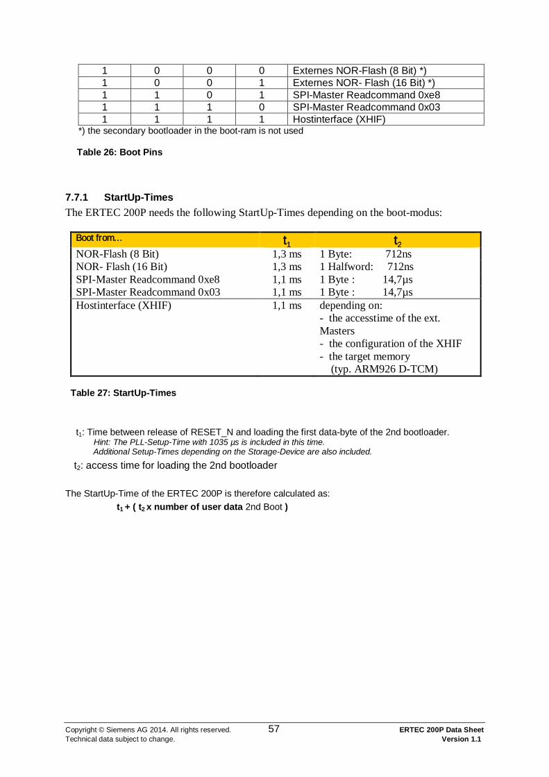
Copyright © Siemens AG 2014. All rights reserved. 57 ERTEC 200P Data Sheet Technical data subject to change. Version 1.1
1 0 0 0 Externes NOR-Flash (8 Bit) *) 1 0 0 1 Externes NOR- Flash (16 Bit) *) 1 1 0 1 SPI-Master Readcommand 0xe8 1 1 1 0 SPI-Master Readcommand 0x03 1 1 1 1 Hostinterface (XHIF)
*) the secondary bootloader in the boot-ram is not used
Table 26: Boot Pins
7.7.1 StartUp-Times The ERTEC 200P needs the following StartUp-Times depending on the boot-modus:
Boot from… t1 t2 NOR-Flash (8 Bit) 1,3 ms 1 Byte: 712ns NOR- Flash (16 Bit) 1,3 ms 1 Halfword: 712ns SPI-Master Readcommand 0xe8 1,1 ms 1 Byte : 14,7µs SPI-Master Readcommand 0x03 1,1 ms 1 Byte : 14,7µs Hostinterface (XHIF) 1,1 ms depending on:
- the accesstime of the ext. Masters - the configuration of the XHIF - the target memory (typ. ARM926 D-TCM)
Table 27: StartUp-Times
t1: Time between release of RESET_N and loading the first data-byte of the 2nd bootloader. Hint: The PLL-Setup-Time with 1035 µs is included in this time. Additional Setup-Times depending on the Storage-Device are also included.
t2: access time for loading the 2nd bootloader The StartUp-Time of the ERTEC 200P is therefore calculated as: t1 + ( t2 x number of user data 2nd Boot )

Copyright © Siemens AG 2014. All rights reserved. 58 ERTEC 200P Data Sheet Technical data subject to change. Version 1.1
8 Thermal Specification ERTEC 200P is intended for use in the operating ambient temperature range -40°C .. +85°C
Example: With P = 1.52W, Ta = 85 °C, 6 Layer PCB and no Air Flow TJ results in TJ = 85°C + 23.5 °C/W x 1.52 W = 120.7 °C The Temperature on the top center of the Package surface results in Tt = 123.1 °C – (0.2 °C/W x 1.52 W) = 120.4 °C With the use of a heat sink
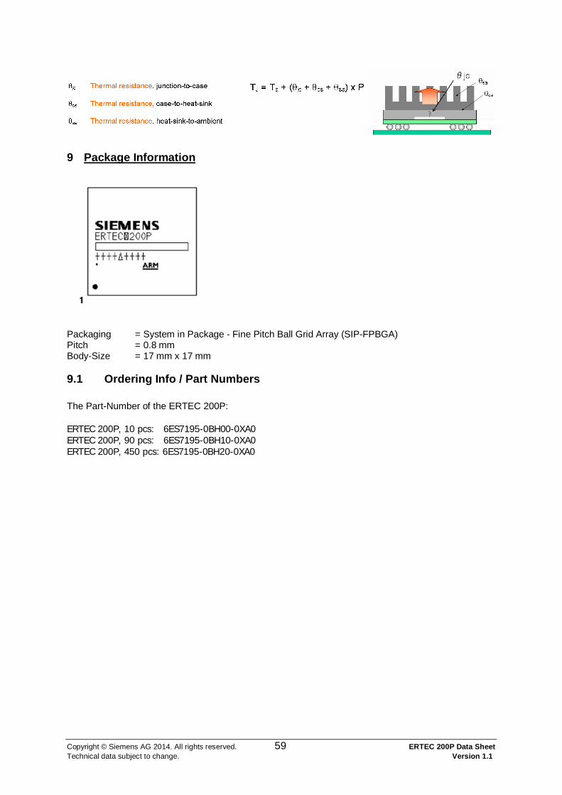
Copyright © Siemens AG 2014. All rights reserved. 59 ERTEC 200P Data Sheet Technical data subject to change. Version 1.1
9 Package Information
Packaging = System in Package - Fine Pitch Ball Grid Array (SIP-FPBGA) Pitch = 0.8 mm Body-Size = 17 mm x 17 mm
9.1 Ordering Info / Part Numbers The Part-Number of the ERTEC 200P: ERTEC 200P, 10 pcs: 6ES7195-0BH00-0XA0 ERTEC 200P, 90 pcs: 6ES7195-0BH10-0XA0 ERTEC 200P, 450 pcs: 6ES7195-0BH20-0XA0

Copyright © Siemens AG 2014. All rights reserved. 60 ERTEC 200P Data Sheet Technical data subject to change. Version 1.1
9.2 400-Pin SIP-FPBGA Package
Figure 28: Package Information

Copyright © Siemens AG 2014. All rights reserved. 61 ERTEC 200P Data Sheet Technical data subject to change. Version 1.1
9.3 Soldering Conditions Solder this product ERTEC 200P (lead free device) under the following recommended conditions:
Soldering Method Soldering Condition Symbol of Recommended Soldering Condition
Infrared reflow
Package peak temperature: 260°C, Time: 60 seconds max. (220°C min.), Number of times: 3 max., Number of days: 7 (see Note)
IR60-107-3
Note: The number of days refers to storage at 25°C, 65% RH MAX after the dry pack has been opened. After that, prebaking is necessary at 125 °C for 10 to 72 hours. For details of the recommended soldering conditions, refer to the information document: Renesas Semiconductor Package Mount Manual
9.4 Packing Information max 90 pices are packed into one tray. The dimensions of a tray are: 135,9mm x 322,6mm x 7,62 mm max. 5 trays are packed into an inner box. The dimensions of an inner box are: 175mm x 375mm x 75 mm

Copyright © Siemens AG 2014. All rights reserved. 62 ERTEC 200P Data Sheet Technical data subject to change. Version 1.1
9.5 Ballout
Figure 29: Ballout ERTEC 200P
10 Quality Information
10.1 Life time / (HW) FIT-Rate Junction-Temperature 125 °C ERTEC 200P Complete 315 Conditions: Ea=0.7eV, C.L=60%, 24h/10yrs
11 Literature / References /1/ ERTEC200P_Manual_en.pdf /2/ ETM9 Technical Reference Manual (Rev. 2a) (ARM DDI 0157E)
20 19 18 17 16 15 14 13 12 11 10 9 8 7 6 5 4 3 2 1
Y20(39) Y19(38) Y18(37) Y17(36) Y16(35) Y15(34) Y14(33) Y13(32) Y12(31) Y11(30) Y10(29) Y9(28) Y8(27) Y7(26) Y6(25) Y5(24) Y4(23) Y3(22) Y2(21) Y1(20)Y 432 424 173 162 159 154 141 314 310 Y
VDD33 GND GPIO28 GPIO29 VDD33 GND CLKP_A GND P2RDXN P2SDXN GND P2TDXN P2FXEN VDD33 GND VDD_EMC D0 D15 GND VDD_EMCW20(40) W19(111) W18(110) W17(109) W16(108) W15(107) W14(106) W13(105) W12(104) W11(103) W10(102) W9(101) W8(100) W7(99) W6(98) W5(97) W4(96) W3(95) W2(94) W1(19)
W 457 434 426 390 386 170 163 160 155 336 316 312 306 WGND GPIO24 GPIO25 GPIO26 REF_CLK XRESET CLKP_B VDD33 P2RDXP P2SDXP VDDQ(PECL)2 P2TDXP TDI RTCK GND VDD_EMC D3 D13 D11 GNDV20(41) V19(112) V18(175) V17(174) V16(173) V15(172) V14(171) V13(170) V12(169) V11(168) V10(167) V9(166) V8(165) V7(164) V6(163) V5(162) V4(161) V3(160) V2(93) V1(18)
V 459 463 436 428 409 405 153 343 324 322 320 291 293 289 VGPIO27 GPIO30 GPIO31 GPIO15_INTGND AVDD AGND VDD15 GND VDD15 TESTDOUT7 GPIO0_INT GND VDD15 D4 D2 D1 D14 D9 D12U20(42) U19(113) U18(176) U17(231) U16(230) U15(229) U14(228) U13(227) U12(226) U11(225) U10(224) U9(223) U8(222) U7(221) U6(220) U5(219) U4(218) U3(159) U2(92) U1(17)
U 465 467 469 470 420 429 384 380 378 376 366 346 341 334 328 323 321 283 285 281 UL_PHY_1 L_PHY_2 GPIO14_INT GPIO13_INTGPIO23 GPIO21 GPIO20 GPIO7_INT GPIO6_INT GPIO5_INT GPIO4_INT GPIO3_INT GPIO2_INT GPIO1_INT DTXR D7 D5 D6 D8 D10T20(43) T19(114) T18(177) T17(232) T16(279) T15(278) T14(277) T13(276) T12(275) T11(274) T10(273) T9(272) T8(271) T7(270) T6(269) T5(268) T4(217) T3(158) T2(91) T1(16)
T 475 471 435 433 427 383 379 377 367 365 327 290 282 277 TGND VDD33 GPIO12_INT GPIO11_INTGPIO10_INTGPIO19 GPIO18 A_PHY_1 A_PHY_2 BYP_CLK GPIO17 GPIO16 TMS TAP_SEL XOE_DRIVER XBE0_DQM0 XCS_PER0 XBE1_DQM1 VDD_EMC VDD_EMCR20(44) R19(115) R18(178) R17(233) R16(280) R15(319) R14(318) R13(317) R12(316) R11(315) R10(314) R9(313) R8(312) R7(311) R6(310) R5(267) R4(216) R3(157) R2(90) R1(15)
R 477 476 478 381 369 370 337 278 275 273 RDVDD3 DGND3 GPIO22 GPIO9_INT GPIO8_INT GND TMC2 VDD33 TACT GND XSRST TEST VDD33 TDO GND XCS_PER1 A23 A22 GND GNDP20(45) P19(116) P18(179) P17(234) P16(281) P15(320) P14(351) P13(350) P12(349) P11(348) P10(347) P9(346) P8(345) P7(344) P6(309) P5(266) P4(215) P3(156) P2(89) P1(14)
P 209 484 485 357 276 249 245 PP2VDDARXTX VDD15 GND XHIF_D2 XHIF_D15 VDD33 GND VDD33 GND VDD12 VDD12 GND VDD33 GND NC A21 XTRST TCK A20 A19N20(46) N19(117) N18(180) N17(235) N16(282) N15(321) N14(352) N13(375) N12(374) N11(373) N10(372) N9(371) N8(370) N7(343) N6(308) N5(265) N4(214) N3(155) N2(88) N1(13)
N 211 213 488 487 250 246 243 239 NP2RXN P2RXP PVSSA XHIF_D10 XHIF_D13 VDD_XHIF VDD_XHIF GND GND VDD12 VDD12 GND GND VDD_EMC VDD_EMC CLK_O_BF1A18 VDD15 A17 XWRM20(47) M19(118) M18(181) M17(236) M16(283) M15(322) M14(353) M13(376) M12(391) M11(390) M10(389) M9(388) M8(369) M7(342) M6(307) M5(264) M4(213) M3(154) M2(87) M1(12)
M 215 217 492 491 474 244 238 240 237 233 MP2TXN P2TXP PVSSA XHIF_D9 XHIF_D6 CTRL_STBY0 GND GND GND GND GND GND GND GND CLK_O_BF2CLK_O_BF0A15 VDD33 A16 XRDL20(48) L19(119) L18(182) L17(237) L16(284) L15(323) L14(354) L13(377) L12(392) L11(399) L10(398) L9(387) L8(368) L7(341) L6(306) L5(263) L4(212) L3(153) L2(86) L1(11)
L 220 219 494 495 497 234 229 231 LVDDACB VSSAPLLCB GND XHIF_D1 XHIF_D5 XHIF_XRDYVDD12 VDD12 GND GND GND GND VDD12 VDD12 GND CLK_I_BF XRDY_BF GND A14 GNDK20(49) K19(120) K18(183) K17(238) K16(285) K15(324) K14(355) K13(378) K12(393) K11(400) K10(397) K9(386) K8(367) K7(340) K6(305) K5(262) K4(211) K3(152) K2(85) K1(10)
K 221 222 223 551 550 232 228 225 223 KVDDAPLL EXTRES ATP XHIF_D8 XHIF_D7 GND VDD12 VDD12 GND GND GND GND VDD12 VDD12 VDD33 XAV_BF XWE_SDRAM XCAS_SDRAM A13 VDD_EMCJ20(50) J19(121) J18(184) J17(239) J16(286) J15(325) J14(356) J13(379) J12(394) J11(395) J10(396) J9(385) J8(366) J7(339) J6(304) J5(261) J4(210) J3(151) J2(84) J1(9)
J 228 226 553 552 556 224 216 217 221 215 211 J P1TXN P1TXP PVSSA XHIF_D14 XHIF_D11 CTRL_STBY1 GND GND GND GND GND GND GND GND CLK_O_SDRAM2CLK_O_SDRAM1XRAS_SDRAM XCS_SDRAM A11 A12H20(51) H19(122) H18(185) H17(240) H16(287) H15(326) H14(357) H13(380) H12(381) H11(382) H10(383) H9(384) H8(365) H7(338) H6(303) H5(260) H4(209) H3(150) H2(83) H1(8)
H 232 230 557 558 208 212 209 207 HP1RXN P1RXP PVSSA XHIF_D4 XHIF_D12 VDD_XHIF VDD_XHIF GND GND VDD12 VDD12 GND GND VDD_EMC VDD_EMC CLK_O_SDRAM0A0 GND A10 A9G20(52) G19(123) G18(186) G17(241) G16(288) G15(327) G14(358) G13(359) G12(360) G11(361) G10(362) G9(363) G8(364) G7(337) G6(302) G5(259) G4(208) G3(149) G2(82) G1(7)
G 234 236 559 560 566 201 204 202 205 179 GP1VDDARXTX VDD15 VDD33ESD XHIF_D0 XHIF_D3 XHIF_XIRQ GND VDD_XHIF GND VDD12 VDD12 GND VDD_XHIF GND XRDY_PERCLK_I_SDRAM A1 VDD33 A7 A6F20(53) F19(124) F18(187) F17(242) F16(289) F15(328) F14(329) F13(330) F12(331) F11(332) F10(333) F9(334) F8(335) F7(336) F6(301) F5(258) F4(207) F3(148) F2(81) F1(6)
F 565 568 67 89 95 178 177 174 FDVDD1 DGND1 VDD33 XHIF_XBE1 XHIF_XBE0 GND XHIF_XBE3 VDD_XHIF TMC1 VDD33 GND CTRL_STBY2 VDD_XHIF XHIF_D17 GND A3 A2 A8 GND GNDE20(54) E19(125) E18(188) E17(243) E16(290) E15(291) E14(292) E13(293) E12(294) E11(295) E10(296) E9(297) E8(298) E7(299) E6(300) E5(257) E4(206) E3(147) E2(80) E1(5)
E 567 569 570 31 34 69 73 75 79 83 91 93 123 133 172 173 EGND VDD_XHIF XHIF_SEG_0 XHIF_A9 XHIF_A7 XHIF_A4 XHIF_XBE2 XHIF_D31 XHIF_D21 XHIF_D30 XHIF_D27 XHIF_D18 XHIF_D16 XHIF_D25 XCS_PER3 XBE2_DQM2 A4 A5 VDD_EMC VDD_EMCD20(55) D19(126) D18(189) D17(244) D16(245) D15(246) D14(247) D13(248) D12(249) D11(250) D10(251) D9(252) D8(253) D7(254) D6(255) D5(256) D4(205) D3(146) D2(79) D1(4)
D 573 575 577 13 19 29 32 68 72 74 78 80 88 90 122 131 166 171 169 165 DXHIF_XWR XHIF_A19 XHIF_SEG_1 XHIF_A15 XHIF_SEG_2 XHIF_A5 XHIF_D28 XHIF_D26 XHIF_D29 XHIF_D22 XHIF_D24 XHIF_D23 XHIF_D20 XHIF_D19 XCS_PER2 D18 D16 XBE3_DQM3 D31 D29C20(56) C19(127) C18(190) C17(191) C16(192) C15(193) C14(194) C13(195) C12(196) C11(197) C10(198) C9(199) C8(200) C7(201) C6(202) C5(203) C4(204) C3(145) C2(78) C1(3)
C 579 583 585 11 18 26 66 47 128 138 144 163 161 CXHIF_XRD XHIF_A12 XHIF_A11 XHIF_A6 XHIF_A16 XHIF_A2 VDD15 XHIF_A14 VDD33 GND VDD15 P1FXEN VDD33 GND VDD15 D20 D17 D30 D27 D28B20(57) B19(128) B18(129) B17(130) B16(131) B15(132) B14(133) B13(134) B12(135) B11(136) B10(137) B9(138) B8(139) B7(140) B6(141) B5(142) B4(143) B3(144) B2(77) B1(2)
B 8 9 12 17 28 30 29 32 45 48 126 134 142 159 BGND XHIF_A10 XHIF_A18 XHIF_XCS_R _A20 XHIF_A3 XHIF_A13 XHIF_A8 GND P1RDXP P1SDXP VDDQ(PECL)1 P1TDXP TESTDOUT5 GND VDD_EMC D19 D22 D25 D26 GNDA20(58) A19(59) A18(60) A17(61) A16(62) A15(63) A14(64) A13(65) A12(66) A11(67) A10(68) A9(69) A8(70) A7(71) A6(72) A5(73) A4(74) A3(75) A2(76) A1(1)
A 10 14 20 30 33 46 49 124 132 140 AVDD_XHIF GND VDD_XHIF XHIF_XCS_M XHIF_A1 XHIF_A17 VDD_XHIF GND P1RDXN P1SDXN GND P1TDXN TESTDOUT6 GND VDD_EMC D21 D23 D24 GND VDD_EMC
20 19 18 17 16 15 14 13 12 11 10 9 8 7 6 5 4 3 2 1


![INVITATION_TO_LOVE_2005 200p 21.1.2011[1]](https://static.fdocuments.in/doc/165x107/577d2ecb1a28ab4e1eb00199/invitationtolove2005-200p-21120111.jpg)