D6.3.115 Demonstration of the secondary substation monitor ...sgemfinalreport.fi/files/D6.3.115...
29
D6.3.115 Demonstration of the secondary substation monitor CLEEN OY Eteläranta 10, P.O. BOX 10, FI-00131 HELSINKI, FINLAND www.cleen.fi D6.3.115 Demonstration of the secondary substation monitor Part1 – Development of secondary substation monitor Bashir Ahmed Siddiqui, Pertti Pakonen, 20 Feb, 2015
Transcript of D6.3.115 Demonstration of the secondary substation monitor ...sgemfinalreport.fi/files/D6.3.115...

D6.3.115 Demonstration of the secondary substation monitor
CLEEN OY Eteläranta 10, P.O. BOX 10, FI-00131 HELSINKI, FINLAND www.cleen.fi
D6.3.115 Demonstration of the secondary substation monitor
Part1 – Development of secondary substation monitor Bashir Ahmed Siddiqui, Pertti Pakonen, 20 Feb, 2015

D6.3.115 Demonstration of the secondary substation monitor
CLEEN OY Eteläranta 10, P.O. BOX 10, FI-00131 HELSINKI, FINLAND www.cleen.fi
1 Introduction In distribution networks, measurement data from primary substation (typically 110 / 20kV) is already available. Due to the introduction of AMR meters, data will also be available from each low voltage customer. However, secondary substations (20 / 0.4 kV) seldom have any remotely readable measurement systems and the existing measurements in the network are mainly limited to frequency range below 2 kHz. As underground cables in cities are aging and cabling of medium voltage networks is also increasing in rural areas, condition monitoring is becoming an important measure in preventing unplanned and long lasting outages. On-line partial discharge monitoring of secondary substation is an excellent way to determine the overall health of the equipment. With the increasing low voltage network challenges due to the introduction of new loads, for example, electrical vehicle (EV), power electronic devices and heat pumps together with increasing demand of high quality power and strict compliance requirements from regulatory authorities, the need for novel multifunction secondary substation monitor is ever increasing.
2 Monitoring functions Monitoring functions such as, PD monitoring, PQ monitoring, disturbance recording and other functionalities i.e. fault detection and location will be equipped with the substation monitor. Rapid fault location based on the secondary substation disturbance recordings (MV/LV) is important in isolating the fault and minimizing the outage duration. PQ monitoring could be used to detect rapid voltage changes, transients and other higher frequency problems which the AMR meters are not capable of measuring.
3 Secondary substation monitor Real-time system measuring and recording high frequency phenomena requires high sampling frequency and much more data processing capacity to capture and process the signals in real-time, thus, FPGA is a promising choice due to low-cost, high speed and great performance. Front end of the system should have wide frequency as well as high enough dynamic range to detect PD and PQ data, respectively. An 8 channel, 12 bits, 65 MHz ADC with serialized LVDS interface has been used for the measurement unit. Secondary substation monitor consists of high speed FPGA+ARM unit, HSMC bride and an LVDS interface analog-to-digital converter. Figure 1 depicts the general architecture of the secondary substation monitor.
3.1 Inductive sensors Essential parts of the on-line monitoring system are the inductive sensors which measure the magnetic field inductively and provide galvanic isolation. Commercial HFCTs are available but they are expensive from the point view of permanent installation. Authors have developed ferrite based low-cost HFCT sensors for continuous on-line monitoring of substation as explained in D6.3.112. The performance of the sensors developed at TUT is compared with the commercial HFCT sensors which show promising results for detecting PD signals [1].

D6.3.115 Demonstration of the secondary substation monitor
CLEEN OY Eteläranta 10, P.O. BOX 10, FI-00131 HELSINKI, FINLAND www.cleen.fi
Fig. 1. General architecture of the secondary substation monitor.
3.2 Band-pass filter Band-pass filter is designed to pass frequencies within a certain range and attenuate frequencies outside that range, which will help to screen out frequencies that are too low or too high, giving easy passage only to frequencies of interest to amplifier input and to avoid aliasing of the sampled signal. Detailed explanation of the active filter amplifier is given in part 2 of this deliverable.
3.3 Analog-to-digital converter (ADC) Front end of the system should have wider frequency range to handle PQ and PD data. Most high speed ADCs have gone to serial outputs like low voltage differential signaling (LVDS) to save pin count and package size. An 8 channel, 12 bits, 65 MHz ADC with serialized LVDS interface has been used for the measurement unit.
3.4 High speed mezzanine card (HSMC) HSMC connectors provide the interface between host board and a mezzanine card. The HSMC-ADC-Bridge enables the output of the LVDS high speed ADCs to be directly connected to a standard HSMC interconnect header. This enables high speed LVDS ADCs to directly interface to FPGA thus saving the time and the cost.
3.5 FPGA LVDS is a common standard for high speed data converters. It uses differential signaling with a P and N wire for each bit to achieve speed up to the range of 1.6 Gbps with double data rate (DDR) or 800 MHz in the latest FPGAs. Most FPGAs have serializer/deserializer (SERDES) block to convert a fast, narrow serial interface on the converter side to a wide, slow parallel interface on the FPGA side. A high speed FPGA+ARM unit i.e. SoCKit with HSMC connector has been used for the data acquisition unit.

D6.3.115 Demonstration of the secondary substation monitor
CLEEN OY Eteläranta 10, P.O. BOX 10, FI-00131 HELSINKI, FINLAND www.cleen.fi
3.6 Signal processing block Signal processing block processes the sampled data to extract the information related to PQ, PD and disturbance recording. It also includes down sampling and frequency domain analysis such as, DFT of the signal to draw the meaningful results. Signal processing algorithms related to PQ and disturbance recording were already developed and implemented as explained D6.3.3. They can be used in the secondary substation monitor together with new algorithm for PD detection.
4 Prototype of the secondary substation monitor Figure 2 depicts the prototype of the secondary substation monitor. A high speed FPGA is interfaced with an 8 channel ADC via HSMC connector.
Fig. 2. Prototype of the secondary substation monitor.
4.1 ADS5282 power supply requirement Power is supplied to the ADS5282 EVM via banana connectors as shown in Figure 3. It can also be noticed that a 100 MHz synthesized arbitrary waveform generator waveform is used to clock the ADS5282 which can be any value between 10 to 65 MHz. Another arbitrary waveform generator is used to input different differential channels. By default, the EVM is configured to use a power management solution to supply the ADC and analog and digital power supplies, allowing users to power the board with a single 5-V power supply. The ADC power management solution is based on TI's TPS77533 and TPS73218, which supply 3.3 V and 1.8 V, respectively. In addition, the EVM offers the capability to supply to the ADC independent 3.3-V analog and 1.8-V digital supplies.

D6.3.115 Demonstration of the secondary substation monitor
CLEEN OY Eteläranta 10, P.O. BOX 10, FI-00131 HELSINKI, FINLAND www.cleen.fi
Fig. 3. Prototype of the secondary substation monitor.
5 8 channels DAQ Unit - Design Principles This section explains the interfacing of 8 channel DAQ system. Capturing data from a serial LVDS interface consists of double data rate (DDR) logic block followed by serial-to-parallel shift register. The DDR block captures input serial data at both edges of the bit clock and outputs two data streams i.e. one corresponding to the rising edge and other corresponding to the falling edge of the bit clock. The rising and falling edge data streams are then applied to the shift register to output the parallel data. The parallel data then goes to the data generation block where they are re-arranged into 12 bits data output. Most FPGAs have a DDR flip-flop and register as part of the logic library. The DDR IO element accepts a single clock and latches the data at the input data pin at both clock edges.

D6.3.115 Demonstration of the secondary substation monitor
CLEEN OY Eteläranta 10, P.O. BOX 10, FI-00131 HELSINKI, FINLAND www.cleen.fi
5.1 Register-transfer level Register-transfer level representation of the individual block taken from Quartus II software is shown below.
Fig. 4. Top level design of the DAQ unit.
Fig. 5. 8 DDR blocks, each handling data from single channel.

D6.3.115 Demonstration of the secondary substation monitor
CLEEN OY Eteläranta 10, P.O. BOX 10, FI-00131 HELSINKI, FINLAND www.cleen.fi
Shift registers to convert serial data from DDR block to parallel output. Next is data generation block to re-arrange the data into proper 12 bits format. Each channel has 2 shift registers i.e. one captures data at rising edge of the bit clock and other captures data at falling edge of the bit clock.
Fig. 6. Shift registers followed by data generation blocks.

D6.3.115 Demonstration of the secondary substation monitor
CLEEN OY Eteläranta 10, P.O. BOX 10, FI-00131 HELSINKI, FINLAND www.cleen.fi
6 Signal-to-noise (SNR) of the secondary substation monitor The dynamic range requirements are high especially in PQ and PD measurements. In PQ measurements relatively low level harmonic components need to be extracted from the voltage or current where the power frequency component is dominating. In PD measurements the variation in pulse magnitude is large and it is necessary to be able to measure correctly both high amplitude pulses originating from discharges close to the sensor and reflections or discharges travelling far from the sensor. Many general purpose measuring systems for example, digital storage oscilloscope, use 8 bits A/D converter which may be insufficient to record the correct shape of the PD pulse. Figure 7 depicts the PD pulse captured by substation monitor and oscilloscope. It is visible from the figure that PD pulse captured by substation monitor is quite smooth compared to oscilloscope because 12-bits substation monitor has 4096 Q levels whereas, 8-bits oscilloscope has only 256 Q levels.
Fig. 7. PD pulse comparison between substation monitor and oscilloscope.
The noise floor limits the smallest measurement that can be taken with certainty since any measured amplitude cannot on average be less than the noise floor. A comparison of the SNR between LeCroy DSO and substation monitor was also made to show the sensitivity of both systems. PD calibrator pulse of 10 000 pC was measured with 12-bits substation monitor and 8-bits LeCroy oscilloscope to calculate the SNR ratio. Both measuring devices were set to the same ± 1 V input voltage range. PD is a sharp pulse having time duration of less than 1 µs, therefore, small portion of the captured data which has PD pulse and same portion of the noise is used to calculate the SNR of both systems.
9.89 9.892 9.894 9.896 9.898 9.9
x 104
-0.05
0
0.05
Time
Am
plitu
de
PD Signal Captured by Substation Monitor & Oscilloscope
Substation Monitor
2.098 2.099 2.1 2.101 2.102 2.103 2.104
x 104
-0.02
0
0.02
Time
Am
plitu
de
Oscilloscope

D6.3.115 Demonstration of the secondary substation monitor
CLEEN OY Eteläranta 10, P.O. BOX 10, FI-00131 HELSINKI, FINLAND www.cleen.fi
Figure 8 depicts the PD signal and noise level captured by substation monitor and oscilloscope. The noise floor of the oscilloscope and substation monitor is calculated as -124dB and -167 dB, respectively. Following equation is used to calculate the SNR of both systems.
SNR(dB) = 20 log10(Signal Vrms / Noise Vrms) The 8-bits oscilloscope has SNR of 12 dB whereas, 12-bits substation monitor has SNR of 38 dB. The secondary substation monitor reduces the quantization noise compared to oscilloscope with 26 dB. Thus, secondary substation monitor is more sensitive and better choice to record the correct shape of the PD pulses buried under noises. In the final implementation the sensitivity will be improved by the filter and amplifier between the PD sensor and A/D converter.
Fig. 8. PD pulse & noise captured by substation monitor and oscilloscope.
7 Demonstration of the whole system This section demonstrate the complete chain of the system which includes high frequency current transformer (HFCT) sensor explained in D6.3.112, band-pass filter and amplifier detailed explanation is given in the next section, 8 channel, 65 MSPS LVDS analog-to-digital converter, FPGA and PC based database. PD waveform data was injected through the cable using 100MS/s arbitrary waveform generator and terminated at 50 Ohms. The HFCT sensor was placed around the cable to measure the PD signal inductively. The output of the sensor goes to the analog-to-digital converter via band-pass filter. Fig. 9(a) depicts the snapshot of the whole system setup in the laboratory and Fig. 9(b)
0.94 0.96 0.98 1 1.02 1.04 1.06 1.08 1.1
x 105
-0.05
0
0.05
0.1
Time
Am
plitu
de
PD Signal & Noise Captured by Substation Monitor & Oscilloscope
Substation Monitor
1.8 2 2.2 2.4 2.6 2.8 3
x 104
-0.01
0
0.01
0.02
0.03
Time
Am
plitu
de
Oscilloscope

D6.3.115 Demonstration of the secondary substation monitor
CLEEN OY Eteläranta 10, P.O. BOX 10, FI-00131 HELSINKI, FINLAND www.cleen.fi
shows DAQ unit along with HFCT sensor and filter. Figure 10 depicts the 12 bits data captured by channel 1 of the secondary substation monitor.
(a)
(b) Fig. 9. (a) Secondary substation setup in the laboratory (b) DAQ unit with HFCT sensor and band-pass filter
D6.3.115 Demonstration of the secondary substation monitor
CLEEN OY Eteläranta 10, P.O. BOX 10, FI-00131 HELSINKI, FINLAND www.cleen.fi
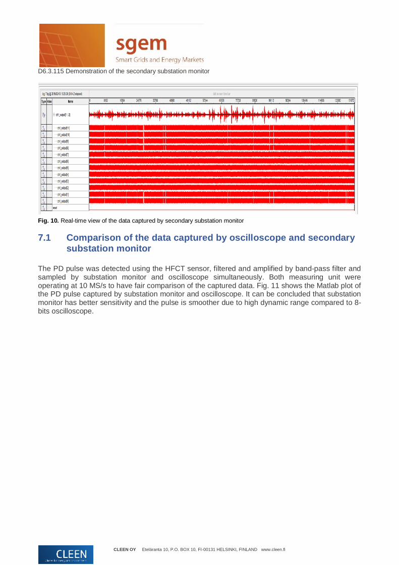
Fig. 10. Real-time view of the data captured by secondary substation monitor
7.1 Comparison of the data captured by oscilloscope and secondary substation monitor
The PD pulse was detected using the HFCT sensor, filtered and amplified by band-pass filter and sampled by substation monitor and oscilloscope simultaneously. Both measuring unit were operating at 10 MS/s to have fair comparison of the captured data. Fig. 11 shows the Matlab plot of the PD pulse captured by substation monitor and oscilloscope. It can be concluded that substation monitor has better sensitivity and the pulse is smoother due to high dynamic range compared to 8-bits oscilloscope.

D6.3.115 Demonstration of the secondary substation monitor
CLEEN OY Eteläranta 10, P.O. BOX 10, FI-00131 HELSINKI, FINLAND www.cleen.fi
Fig. 11. Matlab plot of the PD pulse sensed and captured by whole chain of the secondary substation monitor.
7.2 Database Quartur II software features a SignalTap II Logic Analyzer Editor which allows debugging the design in real-time using wave display. However, post-processing to detect the PD signals requires data to be stored in the database. Therefore, local database has been implemented in the laptop which stores data in comma-separated values (CSV) file from the DAQ unit. Fig. 9 depicts the snapshot of the database which shows real PD data captured by the secondary substation monitor in the laboratory setup explained in section 5.
0 2 4 6 8 10 12
x 104
-0.2
-0.1
0
0.1
0.2
Time
Am
plitu
de
PD pulse captured by substation monitor & oscilloscope
Substation Monitor
0 2 4 6 8 10 12
x 104
-0.1
-0.05
0
0.05
0.1
Time
Am
plitu
de
Oscilloscope

D6.3.115 Demonstration of the secondary substation monitor
CLEEN OY Eteläranta 10, P.O. BOX 10, FI-00131 HELSINKI, FINLAND www.cleen.fi
Fig. 9. SCV file stored in the Database.
8 References [1] Bashir Ahmed Siddiqui, P. Pakonen, Pekka Verho, Novel Sensor Solutions for On-line PD Monitoring”, The 23rd International Conference & Exhibition on Electricity Network, CIRED, Lyon, France, June 2015 (Accepted).

D6.3.115 Demonstration of the secondary substation monitor
CLEEN OY Eteläranta 10, P.O. BOX 10, FI-00131 HELSINKI, FINLAND www.cleen.fi
D6.3.115 Demonstration of the secondary substation monitor
Part2 – Implementation of filter and amplifier Antti Hildén, Pertti Pakonen

- 1 - D6.3.115 Demonstration of the secondary substation monitor
CLEEN OY Eteläranta 10, P.O. BOX 10, FI-00131 HELSINKI, FINLAND www.cleen.fi
1 Design principles The function of the designed filter and amplifier is to prevent low frequencies i.e. 50 Hz and its harmonics (and other low frequency disturbances) from disturbing the partial discharge measurements and, on the other hand to implement anti-aliasing filtering before the A/D-converter of the measuring unit. So the filter has to operate between the sensor and the A/D converter in a way that these waves wouldn’t appear in the output signal fed to the A/D-converter. The main component of the filter is OPA2690 operational amplifier made by Texas Instruments. There are two OPA2690s and two op-amps in each one and all of the op-amps are in use. One is used for low-pass filtering, two for high-pass filtering and the last one for amplifying. In other words we are talking about an active filter amplifier. In case of active filter you have to also get power for the op-amps. To minimize connectors, wiring and distance to a PD sensor the filter is getting the power through output terminal from the measuring unit. The required DC component was added to the same coaxial carrying output signal and directed straight to a operating voltage unit of the device using capacitors and coils. Thus, the filter/amplifier can be installed close to the sensor to improve the system SNR, if necessary. OPA2690 components have a decent single-supply operating and slew rate and the circuits considering filtering are designed obeying Sallen-Key topology. With this simple second order topology it was really easy to achieve steeper passband slopes and better frequency response in general with OPA2690. This kind of simple structures are also easy to multiply. If you think this device as a structure made of several elements you can find the following parts: Low-pass filter, two separate high-pass filters and an amplifier. Rest of the circuits are taking care of the protection of the filter and power delivering to op-amps. Simplified block diagram is depicted in Fig. 1.
Fig. 2. Block diagram of the filter.
Switching between two high-pass filters is done by two jumpers that correspond to switches in the block diagram. Naturally both jumpers have to be in right position in oder to get the filter working. Amplifying is put after the filter although both high-pass filters have some gain too. Low-pass filter is a unit gain filter.
1.1 Filter design Sallen-Key topology is one of the two very popular active filter structures. It is simple to design and requires only few components with reasonable values. The other topology is Multiple Feedback. Sallen-Key topology was chosen to this project. Both low-pass and high-pass filters are made

- 2 - D6.3.115 Demonstration of the secondary substation monitor
CLEEN OY Eteläranta 10, P.O. BOX 10, FI-00131 HELSINKI, FINLAND www.cleen.fi
using Sallen-Key topology and in Fig. 2 and 3 you can see the basic schematic circuit diagrams for the filters.
Fig. 3. Sallen-Key low-pass filter.[1]
Fig. 4. Sallen-Key high-pass filter.[1]
Because the gain of the low-pass filter is one resistor R3 doesn’t exist in the filter circuit. R4 was left to stabilize a gain peak just before the cut-off frequency. In high-pass filters resistors R3 and R4 were used to set the gain of the passband adequate. Resistors R1 and R2 and capacitors C1 and C2 defined the bandwidth. The manufacturer only had some guidelines but there were no specific rules for the values of the components. Simulate and measure was proved to be the best way to get the limits correct because the device had other circuits as well and those affected to the filtering. Of course there were used also a couple of basic equations that gave some good approximate values for the components. The following formula can be used to calculate approximate value for the point where the signal starts to attenuate. Equation 1 is for unit gain filter and valid for both low-pass and high-pass filter.[1]
=1
2 1 2 1 2
(1)
After is computed the final design needs less simulation when effects of the other filters, amplifier and rest of the variables are added. Usually amplifying lowers the high-pass limit and raises the low-pass limit in this device. Values of the components were solved in such a way that
- 3 - D6.3.115 Demonstration of the secondary substation monitor
CLEEN OY Eteläranta 10, P.O. BOX 10, FI-00131 HELSINKI, FINLAND www.cleen.fi
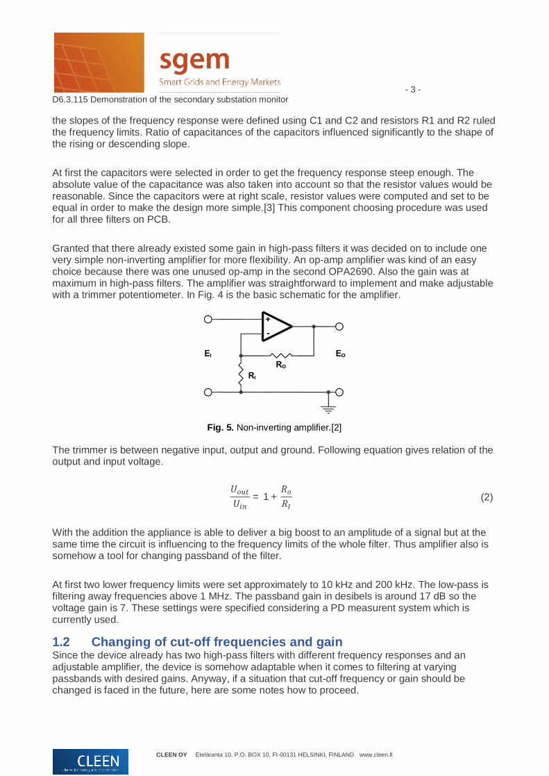
the slopes of the frequency response were defined using C1 and C2 and resistors R1 and R2 ruled the frequency limits. Ratio of capacitances of the capacitors influenced significantly to the shape of the rising or descending slope. At first the capacitors were selected in order to get the frequency response steep enough. The absolute value of the capacitance was also taken into account so that the resistor values would be reasonable. Since the capacitors were at right scale, resistor values were computed and set to be equal in order to make the design more simple.[3] This component choosing procedure was used for all three filters on PCB. Granted that there already existed some gain in high-pass filters it was decided on to include one very simple non-inverting amplifier for more flexibility. An op-amp amplifier was kind of an easy choice because there was one unused op-amp in the second OPA2690. Also the gain was at maximum in high-pass filters. The amplifier was straightforward to implement and make adjustable with a trimmer potentiometer. In Fig. 4 is the basic schematic for the amplifier.
Fig. 5. Non-inverting amplifier.[2]
The trimmer is between negative input, output and ground. Following equation gives relation of the output and input voltage.
= 1 + (2)
With the addition the appliance is able to deliver a big boost to an amplitude of a signal but at the same time the circuit is influencing to the frequency limits of the whole filter. Thus amplifier also is somehow a tool for changing passband of the filter. At first two lower frequency limits were set approximately to 10 kHz and 200 kHz. The low-pass is filtering away frequencies above 1 MHz. The passband gain in desibels is around 17 dB so the voltage gain is 7. These settings were specified considering a PD measurent system which is currently used.
1.2 Changing of cut-off frequencies and gain Since the device already has two high-pass filters with different frequency responses and an adjustable amplifier, the device is somehow adaptable when it comes to filtering at varying passbands with desired gains. Anyway, if a situation that cut-off frequency or gain should be changed is faced in the future, here are some notes how to proceed.

- 4 - D6.3.115 Demonstration of the secondary substation monitor
CLEEN OY Eteläranta 10, P.O. BOX 10, FI-00131 HELSINKI, FINLAND www.cleen.fi
If only cut-off frequency has to be modified, it is recommended to begin the task by adjusting the resistors of the filter. They should be kept equal while applying equation 1. Passband can also be tuned by altering the gain of the amplifier but keeping in mind that then both of the cut-off frequencies change. If there is only need for a greater amplification of a signal only the trimmer of the amplifier should be touched. Little gain adjust doesn’t affect passband considerably but if the trimmer is turned to the other end the passband will alternate a lot too.
1.3 Voltage source and connections To simplify the voltage source of the op-amps and enable powering via coaxial signal cable the filters are operating with a single-supply voltage. In other words there is only positive voltage available and negative voltage pin of the part is attached to the ground. With this kind of solution a DC voltage used as a power of the device could be moved in the coxial cable of the ouput signal. So in practice the measuring unit is supplying the filter via coaxial cable which also holds the partial discharge signal coming from the filter. DC and AC components are decoupled with a coupling capacitor at the both ends. Also there are coils at the DC sides to prevent any high frequency signal entering the voltage source. In order to have single-supply operating you must summarize DC voltage to the signal to be amplified. Otherwise, only the positive amplitudes will be visible at the output of the op-amp. In this design the DC-voltage was generated by means of a simple voltage divider including two resistors in series so that the voltage is half of the supply voltage. The PD signal was added to the DC voltage through a coupling capacitor. All the filter circuits and the amplifier have this DC component in their inputs and outputs but there are coupling capacitors and different voltage dividers at every circuit to ensure the right voltage level. Switching between the high-pass filters has been done with four jumpers. So if you have to change the lower cut-off frequency, there are four jumpers to move. Why to implement four jumpers and not just one or two as it would be logical? It was decided to make the separation in switches very clear to avoid any disturbances. Two 3-pin headers are meant for selecting the correct input and ouput for the right high-pass filter. Whereas the two 2-pin headers are either connecting or disconnecting the negative feedbacks of the op-amps that are used. When the negative feedback of the non-operating filter is disconnected, the disturbance between two op-amps in the same part should be much smaller.
2 Frequency response and other measurements Input and output terminals of the filter are matched to impedance of 50 by placing reasonable resistors. This impedance is compatible with PD sensors and also convenient while doing tests with different kind of devices to ensure a proper impedance matching and so on good test and measurement results. Right after soldering and assembling the filter functioning was tested with an oscilloscope. To power up the device for the tests an external voltage source was used. In practice the operating voltage input was separated from the output terminal and voltage was fed directly to the op-amps. This way there was only AC-component at the output during measurements. The first oscilloscope

- 5 - D6.3.115 Demonstration of the secondary substation monitor
CLEEN OY Eteläranta 10, P.O. BOX 10, FI-00131 HELSINKI, FINLAND www.cleen.fi
test was just to verify that the filter was working like it should. A signal generator was connected to the input and the output was monitored when the frequency of the signal was varied through passband. If the right frequencies were amplified and attenuated most probably assembling was done correctly.
2.1 Frequency and phase responses The next step was to check out a frequency response of the filter. Two frequency sweeps were perfomed using both high-pass filters. At the same time also phase response was recorded. Measurements were completed with network analyzer Agilent 4395A using measurement setup sketched in Fig. 5. Again, external voltage source was powering the op-amps directly in order to avoid DC voltage at the port of the analyzer. In this case it was mandatory to block DC voltage because of the properties of the appliance. When the voltage was supplied straight to the PCB coupling capacitors took care of isolating DC and AC at the input and output.
Fig. 6. Measurement setup with the network analyzer.
S-parameter S21 was used and data points of the frequency sweep were saved to a computer. The noise at low frequencies (below some kHz) is due to the fact that the analyzer is not designed for such low frequencies. Disturbance in response can be seen in Fig. 6 and Fig. 7 that include frequency and phase response while the lower high-pass limit is in use and the amplifier is increasing passband gain.

- 6 - D6.3.115 Demonstration of the secondary substation monitor
CLEEN OY Eteläranta 10, P.O. BOX 10, FI-00131 HELSINKI, FINLAND www.cleen.fi
Fig. 7. Frequency response with lower cut-off frequency and high gain.
Fig. 8. Phase response with lower cut-off frequency and high gain.
After a certain point greater gain at passband starts to distort the shape of the frequency response. A higher gain was wanted anyway so compromises had to be done. The amplification was designed keeping in mind both the shape of the response and the amplitude of the PD pulse. A
-80
-70
-60
-50
-40
-30
-20
-10
0
10
20
30
1 000 10 000 100 000 1 000 000 10 000 000
Gai
n (d
B)
Frequency (Hz)
Frequency response of the filter
-200
-150
-100
-50
0
50
100
150
200
1 000 10 000 100 000 1 000 000 10 000 000
Phas
e (d
egre
e)
Frequency (Hz)
Phase response

- 7 - D6.3.115 Demonstration of the secondary substation monitor
CLEEN OY Eteläranta 10, P.O. BOX 10, FI-00131 HELSINKI, FINLAND www.cleen.fi
discharge of 1000 pC of the PD calibrator was chosen as a reference pulse and an amplitude of the pulse was set to be 100 mV at the output of the filter while lower high-pass limit was selected. The things that influenced to the choices were following: A stronger pulse has better resolution, amplifying could be done without the signal to be cut at larger pulses, response wouldn’t change too much and the shape of the pulse waveform would still be the very same. When the criterias were fulfilled an amplitude of 100 mV was acceptable so a round number was chosen. Finally an amplification of 17 dB was achieved at maximum and the device is able to function with pulses with an apparent charge of 15 000 pC and maybe even higher. Although, it has to be remembered that the amplitude of the PD pulse doesn’t increase linearly with the pulse charge. Either way, the amplitude is a good way to begin estimating a partial discharge. The amplitude of 100 mV was measured when the filter was connected to a usual PD measurement circuit. This circuit is introduced later on in this document in Fig. 14. The frequency and phase responses with the higher high-pass limit were measured and are depicted in Fig. 8 and Fig. 9. It can be seen that the frequency response doesn’t suffer from the higher gain. Some distortion is again visible in the figures but it doesn’t affect the results.
Fig. 9. Frequency response with higher cut-off frequency and high gain.
-100
-80
-60
-40
-20
0
20
40
1 000 10 000 100 000 1 000 000 10 000 000
Gai
n (d
B)
Frequency (Hz)
Frequency response of the filter

- 8 - D6.3.115 Demonstration of the secondary substation monitor
CLEEN OY Eteläranta 10, P.O. BOX 10, FI-00131 HELSINKI, FINLAND www.cleen.fi
Fig. 10. Phase response with higher cut-off frequency and high gain.
Because of the pretty simple PCB and overall structure there were made 12 of these devices. The majority of the filters were set to operate with the high passband gain but there were also a couple of devices that were left to work without so much extra gain. In other words the gain of the amplifier was adjusted so that the response wasn’t affected at all. In Fig. 10 and 11 frequency and phase responses are shown while using lower high-pass cut-off frequency.
-200
-150
-100
-50
0
50
100
150
200
1 000 10 000 100 000 1 000 000 10 000 000
Phas
e (d
egre
e)
Frequency (Hz)
Phase response of the filter

- 9 - D6.3.115 Demonstration of the secondary substation monitor
CLEEN OY Eteläranta 10, P.O. BOX 10, FI-00131 HELSINKI, FINLAND www.cleen.fi
Fig. 11. Frequency response with lower cut-off frequency and lower gain.
Fig. 12. Phase response with lower cut-off frequency and lower gain.
Also the higher limit configuration was measured and results are in Fig. 12 and 13. It is noticeable that passband is more narrow with lower gain and higher and lower cut-off frequencies are moving towards each other.
-80
-70
-60
-50
-40
-30
-20
-10
0
10
20
1 000 10 000 100 000 1 000 000 10 000 000
Gai
n (d
B)
Frequency (Hz)
Frequency response of the filter
-200
-150
-100
-50
0
50
100
150
200
1 000 10 000 100 000 1 000 000 10 000 000
Phas
e (d
egre
e)
Frequency (Hz)
Phase response of the filter

- 10 - D6.3.115 Demonstration of the secondary substation monitor
CLEEN OY Eteläranta 10, P.O. BOX 10, FI-00131 HELSINKI, FINLAND www.cleen.fi
Fig. 13. Frequency response with higher cut-off frequency and lower gain.
Fig. 14. Phase response with higher cut-off frequency and lower gain.
Gains for the filters having less amplifying are approximately 13 dB at highest. A filter with lower gain deals better with larger pulses because of an op-amp maximum output voltage. Thus the filter
-120
-100
-80
-60
-40
-20
0
20
1 000 10 000 100 000 1 000 000 10 000 000
Gai
n (d
B)
Frequency (Hz)
Frequency response of the filter
-200
-150
-100
-50
0
50
100
150
200
1 000 10 000 100 000 1 000 000 10 000 000
Phas
e (d
egre
e)
Frequency (Hz)
Phase response of the filter

- 11 - D6.3.115 Demonstration of the secondary substation monitor
CLEEN OY Eteläranta 10, P.O. BOX 10, FI-00131 HELSINKI, FINLAND www.cleen.fi
can be easily adjusted to work in different environments just by rotating the trimmer potentiometer which changes the gain of the amplifier.
2.2 Filtered PD pulse waveforms One very important point of interest was to find out how different PD signals would change after they had gone through the device. The filter was tested with both filter configurations and the PD pulse was altered. When the waveform of the input and output were verified also noise and delay were observed. The circuit shown in Fig. 14 presents the measuring setup for PD pulses.
Fig. 15. PD pulse measurement setup.
PD calibrator was used as a pulse source and the pulse was driven to 50 impedance. The pulse induced to PD sensor and was led to the input of the filter via coaxial cable. In practice the output signal was measured with a different oscilloscope and using a probe but the computer in Fig. 14 was also connected to provide power for the filter. On the other hand, the idea was to simulate the real measuring situation as well as possible so the computer and a certain PD sensor were added to the setup. The same setup was also used when the gains of the filters were adjusted so that the 1000 pC amplitude was 100 mV. For reference a device with the lower gain and better frequency response as in Fig. 10 and 12 was measured at first. The input and two output pulses can be seen in Fig. 15. The PD calibrator had three different pulse sizes: 100 pC, 1000 pC and 10 000 pC. All of them were used in testing phase but only 100 pC and 1000 pC waveforms are presented here because 10 000 pC didn’t make any difference anymore than a higher amplitude. The discharge of 1000 pC was kept as a some kind of starting point for the design.
Oscilloscope

- 12 - D6.3.115 Demonstration of the secondary substation monitor
CLEEN OY Eteläranta 10, P.O. BOX 10, FI-00131 HELSINKI, FINLAND www.cleen.fi
Fig. 16. PD calibrator pulse of 1000 pC before and after filtering with two different high pass corner
frequencies (~10 kHz and ~200 kHz).
The devices that are usually used for filtering have the higher gain and slightly different frequency response in terms of the shape of the passband and slopes. The frequency responses were presented in Fig. 6 and 8 and it was noted the compromise of the higher gain affected the response. Filtered and more amplified PD pulses are shown in Fig. 16.

- 13 - D6.3.115 Demonstration of the secondary substation monitor
CLEEN OY Eteläranta 10, P.O. BOX 10, FI-00131 HELSINKI, FINLAND www.cleen.fi
Fig. 17. PD calibrator pulse of 1000 pC before and after filtering and amplifying with two different high pass
corner frequencies (~10 kHz and ~200 kHz).
It can be said that the difference in the shapes of the frequency responses doesn’t affect to the pulse waveform significantly. The increase in gain rises the amplitudes but the waveforms could be scaled down and matched to look identical. The higher gain just makes the pulses more visible and the signal-noise ratio decreases. In Fig. 17 a smaller discharge of 100 pC has been used and the pulse waveforms have been measured the same way as before. Now it is noticeable that noise is more apparent but the signals are still behaving as they should and it is possible to measure them. Some of the noise is from the oscilloscope and the rest is generated by the device.

- 14 - D6.3.115 Demonstration of the secondary substation monitor
CLEEN OY Eteläranta 10, P.O. BOX 10, FI-00131 HELSINKI, FINLAND www.cleen.fi
Fig. 18. PD calibrator pulse of 100 pC before and after filtering and amplifying with two different high pass
corner frequencies (~10 kHz and ~200 kHz).
All the filtered waveforms looked like it was expected. The pulse filtered with more narrow passband has a bigger dip in the negative side in consequence of the input signal. At the same time the filter with the lower high-pass limit amplifies the positive amplitude more and produces somehow different waveform. As a conclusion it can be stated that with such a simple filter structure it was rather easy to build a device with very sufficient filtering. The possibilities to increase the gain and change the frequency limits are quite convenient and straightforward to implement.
3 Using filter During real measurements and monitoring the filter is connected between HFCT PD sensor and A/D converter. So in practice the order of the system blocks is more or less the following: PD sensor, PD Op-Amp Filter, A/D converter, processing unit etc. If you are going to start using this filter there are a couple things to keep in mind. Firstly, the filter device needs an operating voltage which should be around 10 V and DC, one volt over or under is still acceptable. The voltage should be added to the output coaxial so the filter can pick it up from there. The second matter is that the filter is recommended to position as near as possible the PD sensor. One of the main reasons of building this device separately of the measuring unit was the fact that a signal could be filtered and amplified so early that a noise in the signal wouldn’t grow too high. There is no point to amplify the noise at the other end of the cable. Also, the measuring unit is usually too big for many places but the filter is light and will fit almost anywhere. The device is approximately 12 cm long, 7 cm wide and 3 cm high. The overall look and PCB of the filter are shown in Fig. 18.

- 15 - D6.3.115 Demonstration of the secondary substation monitor
CLEEN OY Eteläranta 10, P.O. BOX 10, FI-00131 HELSINKI, FINLAND www.cleen.fi
Fig. 19. Open case of PD Op-Amp Filter.
The circuit board is attached inside a painted aluminiun case. The case frame also works as a ground potential. The picture shows the two SMA connectors for the input and output and the jumpers that select the right filters are located at the lower side of the board.
4 References [1] Analysis of the Sallen-Key Architecture, Application Report, Texas Instruments, Sep 2002, Available: http://www.ti.com/general/docs/litabsmultiplefilelist.tsp?literatureNumber=sloa024b [2] Handbook of Operational Amplifier Applications, Application Report, Texas Instruments, Oct 2001, 17 p., Available: http://www.ti.com/lit/an/sboa092a/sboa092a.pdf [3] A Single-Supply Op-Amp Circuit Collection, Application Report, Nov 2000, 15-17 p., Available: https://courses.cit.cornell.edu/bionb440/datasheets/SingleSupply.pdf