CVD Deposition of Group-III Nitride Materials · GaN on Sapphire substrate! The lattice mismatch...
58
1 Department of Electrical Engineering, University of South Carolina, [email protected] Work supported by Army, Navy, DARPA and NASA Outline 1. Why III-Nitrides 2. Material Requirements and Issues 3. Substrate Technology 4. Thick Film Deposition (HVPE) 5. MOCVD Growth 6. MEMOCVD-Digital Epitaxy 7. Ternary and Quaternary Digital Epitaxy 8. Lateral Epitaxial Overgrowth 9. Devices and Conclusions By : Prof. Asif Khan, CVD Deposition of Group-III Nitride Materials
Transcript of CVD Deposition of Group-III Nitride Materials · GaN on Sapphire substrate! The lattice mismatch...

1
Department of Electrical Engineering, University of South Carolina,[email protected]
Work supported by Army, Navy, DARPA and NASA
Outline1. Why III-Nitrides2. Material Requirements and Issues3. Substrate Technology4. Thick Film Deposition (HVPE)5. MOCVD Growth6. MEMOCVD-Digital Epitaxy7. Ternary and Quaternary Digital Epitaxy8. Lateral Epitaxial Overgrowth9. Devices and Conclusions
By : Prof. Asif Khan,
CVD Deposition of Group-III Nitride Materials

2
III-N Materials
InNGaNAlN ?
Breakdown Field approximately 5-10 times of GaAs
3
tle
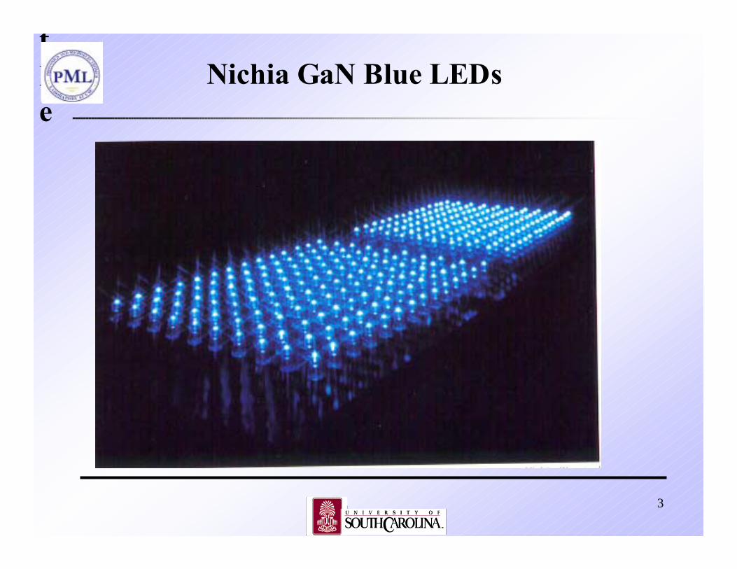
Nichia GaN Blue LEDs

4
Lighting and Display Technologies
GaAs 1980s GaN 1990s
Past and the Present
Lighting
Displays

5
Next Generation Lighting Systems
• Low voltage (< 10 V), Digital Controls• High efficiency, Lifetime > 2 years

6
Purifiers$ 20 billion*
Air
Water
White Lighting $ 10 billion*
Outdoor
Indoor
Bio-Med Sensors$ 10 billion*
Fixed
Portable
ApplicationsDeep Ultraviolet Light Emitting Diodes
* Strategies unlimited , Compound Semiconductors
λ ~ 254 nm λ ~ 265 nm λ ~ 280 nm

7
Technology ApplicationsSilicon GaAs GaN
Power: < 0.1 W/mm 1 W/mm 5-10 W/mmOperation T: 80 C 125 C > 300 C
5 mm
Photonics
Electronics
III-N Materials

8
sapphire
n+-AlGaN barrier
AlN/AlGaN SL
Ti/Al/A
u AlGaN MQW
AlN Buffer
p-AlGaNp+-GaN
Ni/Au
I - SiC
Pd/Ag/Au
GaN
AlN
Pd/Ag/AuAlGaN
S G DSiO2
0.3 µ m
3 µ m
I - SiC
Pd/Ag/Au
GaN
AlN
Pd/Ag/AuAlGaN
S G D
µ m
µ m
I - SiC
Pd/Ag/Au
GaN
AlN
Pd/Ag/AuAlGaN
S G DSiO2
0.3 µ m
3 µ m
I - SiC
Pd/Ag/Au
GaN
AlN
Pd/Ag/AuAlGaN
S G D
µ m
µ m
I - SiC
Pd/Ag/Au
GaN
AlN
Pd/Ag/AuAlGaN
S G DSiO2
0.3 µ m
3 µ m
I - SiC
Pd/Ag/Au
GaN
AlN
Pd/Ag/AuAlGaN
S G D
µ m
µ m
I - SiC
Pd/Ag/Au
GaN
AlN
Pd/Ag/AuAlGaN
S G DSiO2
0.3 µ m
3 µ m
I - SiC
Pd/Ag/Au
GaN
AlN
Pd/Ag/AuAlGaN
S G D
µ m
µ m
I - SiC
Pd/Ag/Au
GaN
AlN
Pd/Ag/AuAlGaN
S G DSiO2
0.3 µ m
3 µ m
I - SiC
Pd/Ag/Au
GaN
AlN
Pd/Ag/AuAlGaN
S G D
SiO2µ m
µ m
I - SiC
Pd/Ag/Au
GaN
AlN
Pd/Ag/AuAlGaN
S G DSiO2
m
µ m
I-SiC
Pd/Ag/Au
GaNAlN
Pd/Ag/Au
n-AlGaN
S G D
LED Microwave Transistors
III-N Device Epilayer Needs
•N- and p-doped Layers•Heterojunctions•Quantum Wells and Superlattices
LEDs and Transistors

Choice of Substrates
Substrate Lattice constant (Angstroms) at 300 K
Thermal Conductivity W/cm-K at 300 K
Thermal expansion coefficient (10-
6 1/K) at 300 K
Bandgap (eV)
GaN a = 3.188 c = 5.185
2.0 3.1 (ave. 300 to 3.5 800 K)
3.39
AlN a = 3.112 c = 4.982
3.2 (c-axis) 2.30 2.69
6.2
6H SiC a = 3.081 c = 15.117
4.9 (a-axis) 2.9 2.9
3.03
4H-SiC a = 3.080 c = 10.082
~3.7 ~2.8 ~2.8
3.26
Sapphire a = 4.765 c = 13.001
0.35 (c-axis) 5.9 6.3
9.9
Si a = 5.4301 1.56 2.57 1.1 GaAs a = 5.6533 0.54 5.8 1.42

-0.160.920.380.38e14, C/m2
850090013510003200µn, cm2/V-s
1.418.22.866.23.390.89EG, eV
5.654.773.083.113.19 3.54 a, A
GaAsAl2O36H-SiC
AlNGaNInN
• No lattice matched substrate• Large polarization effects
Nitride Materials and Possible Substrates
Pd/Ag/Au
Al2O3
n+-AlGaNn-AlGaNn-AlGaNp-AlGaNp-GaN
100 µm
t = 1-5 µm
100 µ
m
LED

Bulk growth of GaN: direct synthesis
Melting conditions of semiconductors (without dissociating)
Equilibrium curve for GaN
Bulk crystal of GaN, grown at 10 – 20 Kbar, and 1400 – 1600 °C without seed, along the 10-10 direction). Squares grids have 1 mm sides
2Ga (melt) + N2 = 2GaN

AlN sublimes dissociatively at the hotter source and condenses reversibly at the colder seed
Sublimation Growth of AlN

15 mm Diameter AlN Boule
Courtesy of Crystal IS

Bulk AlN PVT

Bulk Crystal Growth Facilities
Crystal Growth
GRINDING
CUTTING

(2" dia. ingot )
SiC CRYSTALS
(0001)
(1120)
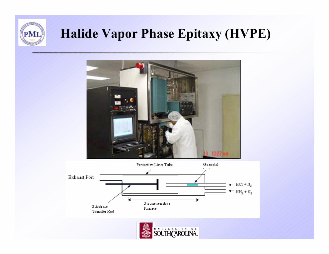
Halide Vapor Phase Epitaxy (HVPE)

Epitaxial Nitride Films by HVPE
! Gallium transport by halide (chloride) formation
2HCl(g) + 2Ga(l) → 2GaCl(g) +H2(g) T = 800 oC
! Reaction with chloride to form the nitride
GaCl(g) + NH3(g) → GaN(s) + HCl(g)+ H2(g); T = 1030 oC
• Growth rate is determined by HCl flux
• High growth rates are possible due to low probability of gas phase nucleation
• Growth rates can exceed 100 mm/min

HVPE GaN
B. Monemar, J Crystal Growth, Vol. 208, p. 18, 2000
Defect Reduction with Thickness

Defects in HVPE GaN Films
Cross section of pit with crack Cross section of crack
Surface with small pits Featureless surface

Free Standing GaN Wafer by HVPE
R. Vaudo, ATMI

Tom Kuech
Growth of AlN & AlGaN by HVPE

MOCVD growth system
NH3
bis-Mg

Various problems associated with mismatches
1.Lattice (a-lattice constant) mismatch
2.Vertical (c-lattice constant mismatch)
3. Coefficient of thermal expansion mismatch
4. Low thermal conductivity
5. Different chemical composition of the epitaxial film
6. Polar surface
Substrate Property Consequence
1. All problems typically associated with high dislocation density
2. Anti-phase boundaries, inversion domain boundaries
3. Thermally induced stress, cracks in epitaxial films
4. Poor heat conduction; unsuitability for high power devices
5. Contamination, interface states, poor wetting of surface during growth
6. Mixed polarity; inversion domains

MOCVD III-N growth issues
Strain/thermal mismatch
Lattice mismatched Substrates
Growth Temperature compatibility
• InN 600 C• GaN 1000 C• AlN 1150 C

SLs buffered
SLs Strain-management for crack-free AlGaN growth

Conventional-MOCVD
MOs
NH3
Surface roughening
Pre-reaction!!!
gas-phase reaction and low surface migration
Growth front
Growth steps

III-N Conventional MOCVD growth
ProblemNative substrates
availablity
Heteroepitaxy
Technology in infancy
Thermal mismatch
resulted cracking
Lattice mismatch induced huge surface
energy difference results in random island
growth
Analogy tomercury on glass
Low T amorphous
AlN/GaN/InNbuffer developed
t
T or flow
T
NH3
MOs
Annealing/nitridation
LT-buffer
growth
Well-established procedure for III-nitrides on sapphire

GaN on Sapphire substrate
! The lattice mismatch with GaN is 13.9%
! The steps for GaN growth includes: (a) Nitridation and (b) low temperature buffer layer (usually AlN) growth
! Growth on c-plane of sapphire gives c-plane GaN, while growth on r-plane gives a-plane GaN
! Energy gap of sapphire is > 8eV so light extraction possible from substrate side for LEDs
Growth steps of GaN on sapphire

Microstructure of GaN on Sapphire

Standard MOCVD vs MEMOCVD
0 10 20 30 40 50 60 70 80 90 100
MOCVD precursor scheme
on
onMOs
NH3
Time0 10 20 30 40 50 60 70 80 90 100
on
off
high
lowNH
3
MOs
MEMOCVD precursor scheme
time
* Gas-phase prereaction
* Low surface mobility* Precursors overlap adjustable * Minimize prereaction and enhance
migration* AlInGaN digital alloys and SLS
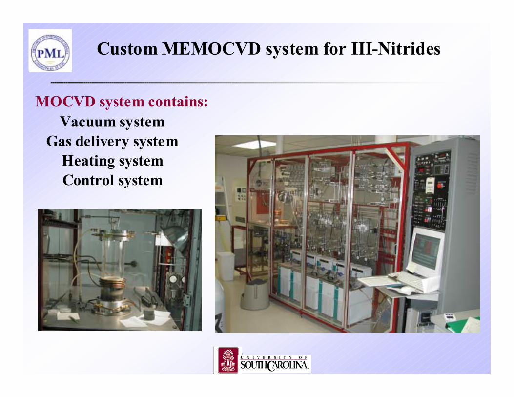
Custom MEMOCVD system for III-Nitrides
MOCVD system contains:Vacuum system
Gas delivery system
Control systemHeating system

MOs
NH3
MEMOCVD of III-N Materials
Minimized pre-reaction
Enhanced migration
allowing V/III separation hence reducinggas-phase reaction & enhancing surface migration
Growth front
Growth steps

MEMOCVD AlN/ALGaN SLs-complex
g=0002
AlGaN
AlN
AlN
AlGaN
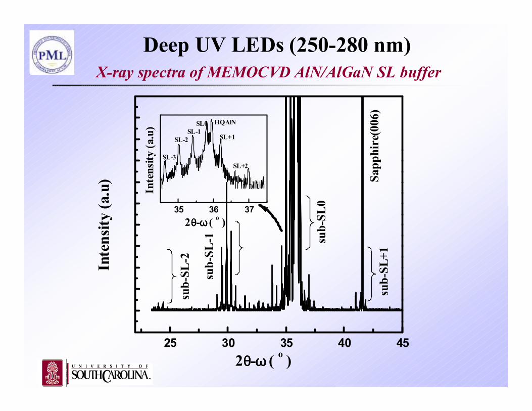
Deep UV LEDs (250-280 nm)X-ray spectra of MEMOCVD AlN/AlGaN SL buffer
25 30 35 40 45
Sapp
hire
(006
)su
b-SL
+1
sub-
SL-2
sub-
SL-1 su
b-SL
0
2θθθθ-ωωωω ( o )
Inte
nsity
(a.u
)
Inte
nsity
(a.u
)
2θθθθ-ωωωω ( o )
35 36 37
HQAlN
SL+2
SL0SL-1
SL-2
SL-3
SL+1

N-AlGaN on MEMOCVD AlN+SLs buffer:Al0.66Ga0.34N for sub-260nm LEDs
RMS=7A with atomic steps
SapphireAlN
AlN
AlGaN
N-AlGaNHigh etch pits density: 1010 cm-2

MOCVD vs MEMOCVD AlN
TMA
NH3
TMA
t
Conventional MOCVD
on
on
t
NH3
PALEon
offonoff
PALE AlNMOCVD AlN

MEMOCVD AlInGaN digital alloys
0 10 20 30 40 50 60 70
-3.0
-2.5
-2.0
-1.5
-1.0
-0.5
0.0
0.5
1.0
1.5
2.0
2.5
TMG
TMI
NH3
TMA
Time (second)
The number of repeats of Al, In, and Ga pulses in the unit cell are 2, 2, and 1, respectively. Pulse length is kept as 6 seconds.

A typical EDAX spectrum for our AlInGaN samples
EDAX In fraction as a function of m, In pulses within one growth unit cell for (3,m,1)
MEMOCVD AlInGaN digital alloys Composition control

MEMOCVD AlInGaN Digital Alloy PL
260 280 300 320 340 360 3800.0
0.5
1.0
1.5
2.0
2.5
(2,2+,1)150
(1,3+,1)150
(3,1,1)150
GaN
PL
inte
nsity
(a.u
.)
Wavelength (nm)
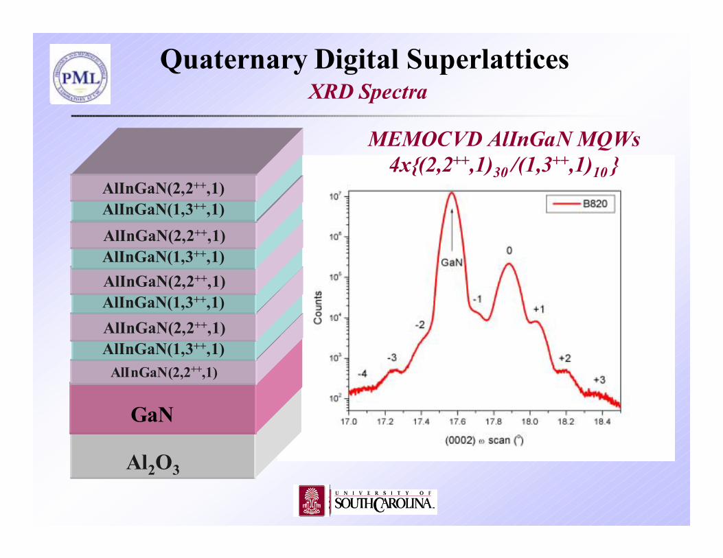
MEMOCVD AlInGaN MQWs 4x(2,2++,1)30 /(1,3++,1)10
GaN
Al2O3
AlInGaN(2,2++,1)AlInGaN(1,3++,1)AlInGaN(2,2++,1)AlInGaN(1,3++,1)AlInGaN(2,2++,1)AlInGaN(1,3++,1)AlInGaN(2,2++,1)AlInGaN(1,3++,1)AlInGaN(2,2++,1)
Quaternary Digital SuperlatticesXRD Spectra

The majority of dislocations in GaN result from the coalescence of misoriented islands
• Dislocations can interact and be annihilated

Stimulated Emission at 258 nm in AlN/AlGaN Quantum Wells Grown on Bulk AlN Substrates

PLOG GaN(IĪ0I)
(IĪ00)(II20)
(1101)(1120)
MOCVD GaN
Figure 2(a)
PLOG GaN
SiO2
(1120)
(1100)
10µm
Completely coalesced PLOG GaN
Pulsed Lateral Overgrowth (PLOG)Different Pulse time for NH3 on and Off

SiC
SiO2
Window region Mask region
2 µm
Low dislocation density
High dislocation density
Pulsed Lateral Overgrowth (PLOG)TEM X-section Image

Complete coalescence of Complete coalescence of GaN GaN by by lateral overgrowth methodlateral overgrowth method
Plane view Cross sectional view
Coalesced film

Surface roughness of PLOG Surface roughness of PLOG GaNGaN
RMS roughness
PLOG GaN = 7-10 Å
* No step termination observed
* Reduction of screw component threading dislocation
05
100150
200
60nm
µm

Device Design
SiO2 mask
Edge Emitting UV LEDs
a-GaN (ELOG)or AlN or c-GaN
R-sapphire / bulk AlN /HVPE GaN
n+(a-GaN) / AlN / GaN
n-AlGaNMQW
p-AlGaNp+-GaN

Non Polar III-N Device Development
R-Sapphire
a-GaN template
a-GaN ELOG
1 st SiO2 mask
2 nd SiO2 mask SALE a-GaN
Approach 2: Selective Area Lateral Epitaxy (SALE)

Step 1. a-plane GaN pillar on R-plane Sapphire
SEM image of fully coalesced
SALE a-plane GaN layer
Non Polar III-N Device DevelopmentSelective Area Lateral Epitaxy (SALE)
Step 2. a-plane GaN pillar after SiO2 deposition
10 µµµµm

a-plane GaN Template, ELOG, SALE
Template:RMS ~ 50 A
ELOG:RMS ~ 4.5 A
SALE:RMS ~ 4.5 A
RMS surface Roughness

X-Ray Rocking Curve Comparison a-plane GaN
a-plane GaN Template, ELOG, SALE

362 nm Peak Emission LED over r-sapphire
Edge Emitting Non Polar UV LEDs
300 350 400 450 500 550 600
100 mA
50mA
20mA
Inte
nsity
, a.u
.
Wavelength, nm
0 2 4 6 8 100
10
20
30
40
50
Rd = 65 ΩΩΩΩ
Cur
rent
, mA
Voltage, V
C. Chen et. al. Jpn. J. Appl. Phys., 42, Part 2, No. 9A/B, pp. L1039-L1040 (2003).

SALE a-plane GaN cavity
]0211[
]1001[
[0001]
N2-laser beam path
Lasing emission
364 366 368 370 372 374 376 378 380
0
200
400
600
800
1000 T = 300 K
270 kW/cm2
330 kW/cm2
400 kW/cm2
500 kW/cm2
Inte
nsity
, a.u
.
Wavelength, nm
Edge Emitting Non Polar UV Laser

Deep UV LEDs (250-280 nm)I-V and Spectral Emission
200 300 400 500
100 µµµµm x 100 µµµµm
Inte
nsity
, a.u
.
Wavelength, nm
0 2 4 6 8 100
10
20
30
40
50
255nm90ΩΩΩΩ
265nm40ΩΩΩΩ
280nm 30ΩΩΩΩ
Cur
rent
, mA
Voltage, V

Deep UV LEDs (250-280 nm)Pulsed powers
280 nmEQE 0.355%WPE 0.122%
265 nmEQE 0.217%WPE 0.107%
0 200 400 600 800 1000 1200 1400 16000
5
10
15
20
25
280 nm267 nm
Northwestern
265 nm
280 nm
500ns, 0.5%
2 x 2 array of 100 µµµµm x 100 µµµµm
Po
wer
, mW
Current, mA

Dr. Hongmei WangDr. E. KuokstisDr P. MaruskaDr. Mikhail Gaevski
Dr. Grigory SiminDr. Alex KoudymovDr. Max Shatalov
RESEARCH
TEAM
Dr. Jinwei YangDr. Wenzhong SunDr. Changqing ChenDr. C. Kim
Dr. Vinod AdivarahanDr. Ashay ChitnisMs. Irina MokinaDr. Y. LeeDr. H. Cho
StudentsMs. Husna FatimaMs. Gong ZhengMr. Ping HuangMr. M. IslamMr. Salih SaygiMr. Wenhua GuMr. J. WangMr. J. LiMr. Shiva RaiMr. Shuai WuMr. A. SattuMr. Z. YangMr. N. Tiperneni
Professor Asif KhanPML Integrated AlGaN Research Team
SupportMr. Ahmad HedariMr. Bin ZhangMr. D. JohnsonMs. Quinhua ZhangMs. T. OsborneMs. Pat Dedman
Matl. Growth
Matl. Test
Device Process
Device Test
Scientist

PML
Photonics Microelectronics Lab 20,000 sq. ft. class 100 clean rooms
Materials
Matl. Testing
Lithography Device Process
Device Package
Electrical TestOptical Test