Cutting-edge PCB - EEWeb...
17
February ‘16 PCB Technology for Wearable Devices 3D Printed Circuit Boards Cutting-edge PCB Prototypes Royal Circuits Innovates Through Investments in Technology and Employees Interview with Milan Shah – President of Royal Circuits ▲ ▲
Transcript of Cutting-edge PCB - EEWeb...

February ‘16
PCB Technology for Wearable Devices
3D Printed Circuit Boards
Cutting-edge
PCB PrototypesRoyal Circuits Innovates Through Investments in Technology and EmployeesInterview with Milan Shah – President of Royal Circuits
▲▲

CLICK HERE
EEWeb
Modern Printed Circuits CONTENTS
4 14
246
EDITORIAL STAFFContent EditorAlex Maddalena [email protected]
Digital Content ManagerHeather Hamilton [email protected] Tel | 208-639-6485
Global Creative DirectorNicolas Perner [email protected]
Graphic DesignerCarol Smiley [email protected]
Audience DevelopmentClaire Hellar [email protected]
Register at EEWebhttp://www.eeweb.com/register/
Published byAspenCore
950 West Bannock Suite 450
Boise, Idaho 83702 Tel | 208-639-6464
Victor Alejandro Gao General Manager Executive Publisher
Cody Miller Global Media Director
Group Publisher
NEWSWIRE
Innovative Projects and Designs at Embedded World 2016
TECH REPORTS
Streamlining Assembly with Flexible and Flex-rigid PCBs
Next-generation 3D Printed Electronics
EEWEB FEATURE
Redefining Small: NexLogic Eyes the Wearables Market with Tiny PCB Packages
INDUSTRY INTERVIEW
Cutting-edge PCB PrototypesInterview with Mlian Shah – President of Royal Circuits
4
14
6
20
24
eeweb.com/register
Join Today

54
Modern Printed Circuits NEWSWIRE
Source: www.eeweb.com/company-news/
Newswire
Digi-Key Electronics will be discussing with attendees how the company’s business model and updated designs tools can help the design engineer with their entire design process at the 2016 Embedded World conference in Nuremberg, Germany.
“We want to remind our European customers that we offer the world’s largest selection of electronic components in stock and ready for immediate shipment,” said Hermann Reiter, Director of Sales for Central & Eastern Europe. “As a 100% franchised distributor, engineers can rest easy knowing their parts are coming directly from the manufacturer and we ship it to their front doors in as little as 24 to 48 hours.”
The company offers customers and engineers numerous value-added services including a variety of low-cost and professional EDA tools; reference, article and video libraries that offer ‘how to’ videos such as Another Geek Moment and Product Training Modules (PTMs); online technical support 24/7 via digikey.com and eewiki.net; extensive BOM tool; and more.
Digi-Key’s booth is located in Hall 4A, Stand 631 and the company, as well as numerous suppliers, will have representatives present to show attendees how easily various products can be used in their own developments. Also to be discussed is how Digi-Key offers a head start with their value-added services as well as programming examples, free source code or technical support.
Innovative Projects and Designs at Embedded World 2016
Attendees are encouraged to stop by the booth to view various live demos, including:
• Thermal Imaging with FLIR Infrared Camera displayed on a Newhaven LCD display This demo shows how to use the FLIR Infrared Camera easily under Linux with a BeagleBone and how to display a live image
• Weather Station with TE Connectivity Sensors and BLE Connection See how a BLE Connection can be established and how the sensor data can be transferred
• Display Sensor Data via Panasonic BLE on a Newhaven Touch Display with a Microchip PIC24 System This demo visualizes the sensor data from the above weather station via the established BLE Connection and displays it on a Newhaven Touch Display
• Trinamic stepper motor controller and driver with Digi International XBEE Wi-Fi Module Try out different modes in how to control stepper motors and learn about the differences
• Neural Network Pattern recognition solution with Cognimem Take the first steps with Neural Networks and learn how easy it can be used
• Wireless Charging with an IDT Solution and display the charge via wireless connection Wireless charging arrives more and more within different industrial products; learn how to charge a super cap and display the charge via wireless transfer on a small LCD-Display
• IoT Sensors via GSM with Nimbelink on a BeagleBone Learn how to transfer sensor data via a GSM Connection to the cloud
• Learn about key updates to Digi-Key’s Scheme-it and PCBWeb design tool offerings and get to know the company’s newest EDA tools
“The Digi-Key motto is ‘by engineers for engineers’,” added David Sandys, Director, Technical & Strategic Marketing. “We were started by an engineer and we work hard to maintain our commitment to be the best place to search, find, and buy electronic components 24/7.”

TECH REPORT
76
Modern Printed Circuits
Streamline Assembly and Improve Reliability with
Expensive and complicated discrete
interconnection cables can reduce a design’s
reliability, increase design cost, and increase
overall design size. Fortunately there is an
alternative in the form of flexible and flex-
rigid PCBs. Flexible PCBs can provide a cost-
effective and convenient solution to your
design’s interconnection requirements, with the
added advantage of having the repeatability
and reliability of a PCB. Where as discrete
interconnections have inherently different
conductor orientations, flexible PCBs hold all
conductors in fixed special orientations to each
other. This consistency of composition allows
for the precise modeling of flexible PCB traces
and a more predictable design. Additionally,
flexible PCBs can include gold finger contacts
allowing for the edge of a flexible PCB to serve
as the male portion of a connector and can
accommodate high-density designs. As such,
flexible PCBs can be used to replace the vast
majority of traditional discrete interconnection
solutions while still allowing for a highly
modular design.
Flexible and Flex-rigid PCBs
Flexible PCBs can provide you with a cost-effective and convenient solution to your design’s interconnection requirements, with the added advantage of having the repeatability and reliability of a PCB.
By PCBCart
TECH REPORT
98
Modern Printed Circuits
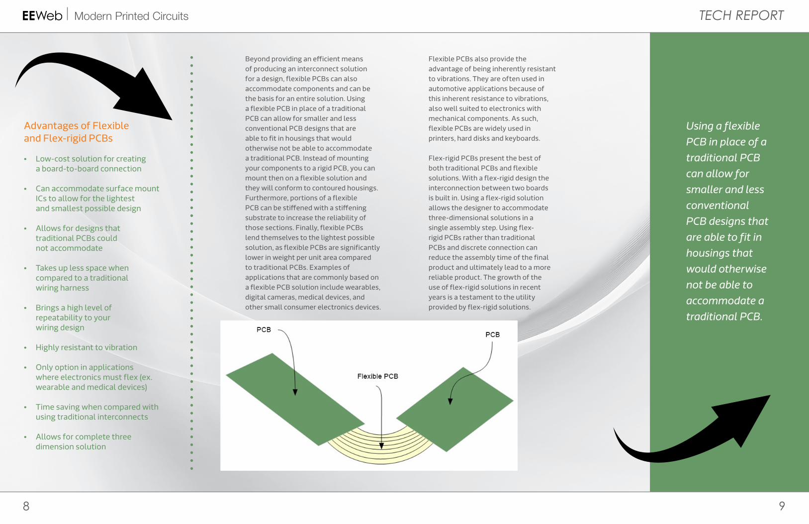
Beyond providing an efficient means of producing an interconnect solution for a design, flexible PCBs can also accommodate components and can be the basis for an entire solution. Using a flexible PCB in place of a traditional PCB can allow for smaller and less conventional PCB designs that are able to fit in housings that would otherwise not be able to accommodate a traditional PCB. Instead of mounting your components to a rigid PCB, you can mount then on a flexible solution and they will conform to contoured housings. Furthermore, portions of a flexible PCB can be stiffened with a stiffening substrate to increase the reliability of those sections. Finally, flexible PCBs lend themselves to the lightest possible solution, as flexible PCBs are significantly lower in weight per unit area compared to traditional PCBs. Examples of applications that are commonly based on a flexible PCB solution include wearables, digital cameras, medical devices, and other small consumer electronics devices.
Flexible PCBs also provide the advantage of being inherently resistant to vibrations. They are often used in automotive applications because of this inherent resistance to vibrations, also well suited to electronics with mechanical components. As such, flexible PCBs are widely used in printers, hard disks and keyboards.
Flex-rigid PCBs present the best of both traditional PCBs and flexible solutions. With a flex-rigid design the interconnection between two boards is built in. Using a flex-rigid solution allows the designer to accommodate three-dimensional solutions in a single assembly step. Using flex-rigid PCBs rather than traditional PCBs and discrete connection can reduce the assembly time of the final product and ultimately lead to a more reliable product. The growth of the use of flex-rigid solutions in recent years is a testament to the utility provided by flex-rigid solutions.
Advantages of Flexible and Flex-rigid PCBs
• Low-cost solution for creating a board-to-board connection
• Can accommodate surface mount ICs to allow for the lightest and smallest possible design
• Allows for designs that traditional PCBs could not accommodate
• Takes up less space when compared to a traditional wiring harness
• Brings a high level of repeatability to your wiring design
• Highly resistant to vibration
• Only option in applications where electronics must flex (ex. wearable and medical devices)
• Time saving when compared with using traditional interconnects
• Allows for complete three dimension solution
Using a flexible PCB in place of a traditional PCB can allow for smaller and less conventional PCB designs that are able to fit in housings that would otherwise not be able to accommodate a traditional PCB.

TECH REPORT
1110
Modern Printed Circuits
Other design tips include:
• Consider staggering traces from layer to layer on flexible circuits to offer higher levels of flexibility.
• Conductors should always be routed perpendicular to a bend radius to aid in reliability and flexibility.
• Termination areas should be stiffened using stiffeners.
• Shielding should be done using a crosshatch pattern rather than with solid planes.
• Through holes should be kept away from bend areas.
Before sending a design for fabrication, consider that your flexible board is bendable in the design process and design the board to have the highest density possible when nested on the productions board. If bend can be used to achieve a particular dimension then make
that bend in the installation and not in the initial design. Finally, using stiffeners with a flexible PCB may be a more cost effective solution than a flex-rigid design. When you only require a low number of layers in a design it may be more cost effective to use a flexible PCB with stiffeners added at critical portions of the board. It’s only when your design has a very large layer count requirement that you should consider a flex-rigid solution.
Finally, while populating a flexible PCB is a very similar process to that of populating a traditional PCB. Consider the following tips when populating your flexible PCBs:
• Bake your flexible PCBs for an hour before populating them to eliminate any absorbed water.
• Fix your flexible PCB to a hard surface to provide dimension stability while soldering to the device.
• When hand soldering devices to a flexible PCB, jump around soldering dense pinned devices to avoid overheating portions of the flexible PCB.
In summary, flexible and flex-rigid PCBs can greatly reduce the cost and complexity of the manufacturing process of your next product. Flexible PCBs are excellent replacements for traditional discrete wiring solutions, offering the repeatability and reliability of PCBs in a flexible form factor. Furthermore, flex-rigid PCBs offer the opportunity to create highly complex three-dimensional designs while maintaining low assembly cost, high levels of repeatability and
reliability. Simply put, flexible PCBs will allow you to tackle designs that would otherwise be cost prohibitive, overly complex to manufacture or simply impossible. Take your design to the next level with a flexible or flex-rigid based PCB.
Here are two samples of flex-rigid PCBs fabricated by PCBCART, one of leading PCB manufacturers based in China.
The design process for a flexible or flex-rigid solution is very similar to that of a traditional PCB board, with the added caveat that the flexible portion of the board needs to be paid special attention with regards to mechanical qualities. Once the two dimensional layout of a flexible design has been created, it’s a good idea to create a mock up of your flexible design using 3D modeling software or to create a paper mock up of the design. Using this method enables you to test whether the design conforms to the mechanical specifications of the flexible substrate. Apart from this, your design does not require a bend radius smaller than that tolerated by the flexible PCB. IPC-2223 can be consulted to determine the minimum bend radius of a particular design.
For quality flexible or flex-rigid PCB fabrication services, please visit www.pcbcart.com. As one of top PCB manufacturers based in China, PCBCART has been offering quick-turn prototype through full production on a wide range of PCB manufacturing for customers who value manufacturability, reliability and timely delivery since 2005. We would be glad to fabricate your next flexible or flex-rigid PCB design and make your next project a success. Here’s what we can do:
• Accommodate designs between 1 and 8 layers on DuPont PI or Domestic Shengyi PI substrates
• Full specifications are available in our flexible/flex-rigid PCB specifications section
• Offer small quantity flexible or flex-rigid PCB turnkey solution
We are now offering new customers 15% discount, up to $200 OFF for their first order with us as a welcome gift. Check our website to get more details.
Layer: 10Thickness: 2.0 mmMaterial: PI and FR4Surface finish: HASLTechnique characteristics: Flex and rigid material combinationApplication: Medical device/Automation/Telecommunication
Flex-rigid PCBs fabricated by PCBCART
Layer: 8Thickness: 1.6 mmMaterial: PI and FR4Surface finish: ENIGTechnique characteristics: Flex and rigid material combinationApplication: Medical equipment/Aerospace

TECH REPORT
1514
Modern Printed Circuits
Nano Dimension Provides Prototypes in all Shapes and Sizes
Most of the world now knows what 3D printing is and what it is capable of. It has obvious benefits for a range of industries, from aviation to medical, engineering practices, and even art and fashion. While 3D printing is already having a disruptive influence on these industries—in the form of product innovation, shorter time-to-market and cheaper development and manufacturing— there is another sector that is only just beginning to understand the great advantages to incorporating additive manufacturing: the electronics industry.
Printed Electronics
Next- generation3D PRINTED PCB PROTOTYPE WAS CREATED WITH NANO DIMENSION’S 3D PRINTER.
By Simon Fried, Chief Business Officer and Co-founder of Nano Dimension

TECH REPORT
1716
Modern Printed Circuits
3D Printed Electronics Gaining MomentumPrinted circuit boards (PCBs) are undoubtedly one of the most important aspects of any electronics product. For decades, electronic device makers have used complex, labor- and material-intensive processes such as photo polymerization, chemical etching, drilling, plating, pressing, and lamination to manufacture PCBs. Product designers requiring PCB prototypes generally have to have them made off-site by specialist sub-contractors. This leaves them the choice of managing slow turnaround processes of two to three weeks, or having to accept very high development costs for a quick turn-around.
Given the tight timeframes usually involved in development projects of this kind, there is a high likelihood of multiple design iterations so that the PCB can be optimized from a circuit and system perspective, which can be frustrating for designers. The risk inherent in the design and prototyping process is such that this process often leads to very conservative PCB designs.
Electrifying Design As was true with other industries, rapid prototyping by 3D printing will lead to significant time and cost savings in PCB design as well as test cycles, higher efficiency, and higher quality. But this is not all; it will also contribute to more flexible and iterative design processes, enabling teams to experiment and
redesign with ease. 3D printing also means that the future of electronics will not be dictated by the rectangular board of a PCB, rather, circuits will be printed within objects and will be able to play a structural role. The creativity of the designer, the properties of the printed materials (both electrical and mechanical), and the free-form nature of circuitry will allow for dramatic changes to what end-products look like and how they function.
The possibilities are endless for rapid prototyping structural electronics, embedded components and sensors, multilayered wiring, and new geometries. The vertical and horizontal PCB will make way for the offset via or the fully printed coil. Having the ability to print a variety of rigid or flexible substrates, even within the same object, could lead to the discovery of totally new application of products, in all shapes and sizes imaginable. Just imagine it: developers, engineers, and product designers will be able to 3D print a round mobile phone with embedded electronics, including a flexible circuit board that bends with interconnections and connections in places currently unimaginable, in a matter of hours. In this way, 3D printed electronics has the potential to play a primary role in keeping up with the changing needs of customers for device miniaturization and customization, as well as rapid changes in markets like IoT, flexible smartphones, displays, and wearables.
Early Days of AdoptionToday, 3D printed electronics is where regular 3D prototyping was about seven years ago, starting to gain awareness but still in the very early stages of adoption. With the obvious benefits of 3D printing in other industries, it is clear why PCB designers and electronics engineers are enthusiastic for it to replace some, if not all, of today’s traditional processes for in-house development of high-performance electronic device applications.
This will not happen overnight, and is unlikely to totally replace traditional manufacturing of electronics. But we can expect 3D printing to shape the
products of tomorrow, enabling them to look and function completely differently. This growth is largely dependent on the right combination of deposition technology, advanced material solutions, and software advancements. To succeed it will also require the discovery of applications where 3D printed electronics can provide unmatched value in terms of speed, ROI, IP security for projects and design compared to traditional manufacturing. Additive manufacturing also offers significant advantages over traditional methods, as it is a zero-waste process with minimal environmental impact.
NANO DIMENSION DRAGONFLY 2020 3D PRINTER
The possibilities are endless
for rapid prototyping structural
electronics, embedded
components and sensors, multilayered
wiring, and new geometries.
Additive manufacturing
also offers significant
advantages over traditional
methods, as it is a zero-
waste process with minimal
environmental impact.

Schematics.com
18
Modern Printed Circuits
Your Circuit Starts Here.Sign up to design, share, and collaborate
on your next project—big or small.
Click Here to Sign Up
Companies developing systems for 3D printed electronics face many challenges. It not only requires the development of very precise new hardware with three axes, but also high performance functional ink formulations offering properties such as conductance, controlled impedance, resistivity engineered to deliver the right amount adhesion and offering specific mechanical properties. Moreover, it requires the development of advanced software to effortlessly convert standard PCB Gerber design files into a 3D printable file. Software for the design and validation of freeform circuit geometries will also become necessary.
The first commercially available 3D PCB printer will be Nano Dimension’s DragonFly 2020 3D Printer. It is a highly accurate and versatile inkjet deposition system for printing multilayer circuit boards. The innovative hardware and dedicated nano-inks bring new possibilities to a wide range of R&D, prototyping, and custom manufacturing projects. Nano Dimension is also developing highly conductive silver nano-inks and high performance dielectrics for use with the printers, as well as novel software enabling Gerber file printing to be seamlessly integrated into the 3D printer. The DragonFly 2020 3D Printer features a printing size of ca. 20cm x 20cm x 0.3 cm. The 3D printer prints ca. 90 µm (3.5 Mil.) traces of conductive and dielectric ink, based on current performance figures.
PCB 3D Printing ProcessThe process of creating a 3D printed PCB prototype starts with the DragonFly 3D Printer depositing two materials, one conductive and one dielectric, in order to build a complete multi-layer PCB from the bottom up. Each pass of the printhead deposits dielectric or conductive nano-ink at the exact location specified by the Gerber design file.
Starting from the underside conductive traces, the materials are built up to finish with the topside conductors. This process means that vias are also built up, either as blind, open or complete vias. Through-holes are also created by repeatedly leaving a space at a particular XY coordinate, thereby building materials up around a void. The dielectric ends up as a solid piece, within which the conductive traces are positioned at the precise XYZ coordinate specified.
3D printed electronics is rapidly developing to be at the forefront of 3D printing technology, and as more and more designers and engineers begin to understand the benefits, it will undoubtedly be utilized to speed development of next-generation electronics—in all shapes and sizes imaginable.
Starting from the underside
conductive traces, the materials are built up to finish with the topside
conductors.

2120
EEWeb FEATUREModern Printed Circuits
NexLogic Eyes the Wearables Market with New Frontier of Tiny PCB Packages
While many leading technology companies have no problem finding success by supporting well-established industries, it’s fair to say that it takes a special brand of ambition to choose to approach new and open-ended avenues of innovation instead. Certainly, every industry is subject to its own forces of change and the necessity for creative evolution, it’s a different kind of challenge when processes are still being defined and the need to invent some of the devices and tools that are required to get the job done becomes a primary concern.
RedefiningSmall

2322
EEWeb FEATUREModern Printed Circuits
This is the case for NexLogic, a one-stop PCB design company based in San Jose, California. At
the start of its 21st year, NexLogic, and company President Zulki Khan, are set on something that’s on the minds of a lot of today’s consumer and commercial industries alike: wearable technology. In a recent interview with EEWeb, Khan spoke about NexLogic’s successful approach to the burgeoning wearables market and what new opportunities lie ahead for PCB companies in this new frontier.
Taking advantage of a network of the world’s newest and smallest components, including powerful chips, innovative power supplies, and next-generation circuit substrates, the wearables industry stands in relatively stark relief from the traditional
PCB world. Rather than working with a wide selection of compatible options in the traditional sense, Khan observes that with wearables, “selection of components is particularly important.” In such a small space, every little bit counts. For one, “power management and battery selection are huge factors when it comes to working with an increasingly small area,” Khan says.
Further, the advent of flexible circuits has helped to give wearable design a new platform all its own, in both a literal and figurative sense. Rather than providing a library of standardized designs, however, most of today’s flexible circuits “have
their own nuances in terms of design and manufacture,” Khan explains, “because there are a lot more applications that aren’t conventional.” With these observations in mind, it appears the general trend for customization in the modern age has got plenty more to inspire in the function and design of similar technology in the near future.
Along with sophisticated power circuits and flexible substrates, it’s also thanks to an entirely new class of powerful microprocessor, including devices like FPGAs and SoCs (systems-on-chips), that such small products continue to do more and more. As Khan points out, “the increasing necessity of these kinds of scaled-down components in today’s innovative technologies brings with it a host of other details that will require their own measures of innovative refinement to further maximize what the new technology can do.”
Today, companies looking to enter the wearables market must be prepared to contend with a whole new level of requirements, particularly when it comes to dealing with the sheer size factor at hand. “In a small wearable device,” Khan says, “the real estate of the PCB is of utmost concern. This is especially true when you are using the smallest packages such as a 01005, which is barely bigger than a grain of salt.”
Likewise, many traditional inspection methods also fail to meet these needs as well. “You cannot use the automated
equipment like an automated optical inspection machine to read the components,” Khan adds. It’s apparent that, as he makes clear, “the traditional way of inspecting and debugging pales when you are talking about these components.” Size is certainly the main factor, but with size comes many concurrent considerations.
While there may certainly be many pitfalls, NexLogic is a company with expertise to share. Khan continues to describe the increasing, multilayered complexity of wearable devices, which affects every level of their creation and makes specialized knowledge more valuable than ever. “To do this requires special types of machines, as well as the manufacturing processes and tolerances—everything comes into play,” he says.
Naturally, leading the way involves a strong dedication to constant research and development, and NexLogic has also provided R&D services to a variety of other companies that have successfully entered the wearables market in recent years. The interplay of materials like experimental epoxies and the need for special shielding between components subjected to the effects of increased proximity stand as only a small example of the issues that the company has
TODAY, COMPANIES LOOKING TO ENTER THE WEARABLES MARKET MUST BE PREPARED TO CONTEND WITH A WHOLE NEW LEVEL OF REQUIREMENTS, PARTICULARLY WHEN IT COMES TO DEALING WITH THE SHEER SIZE FACTOR AT HAND.
helped its clients to conquer, setting new standards in the industry along the way.
In offering some general counsel to those looking to make the move toward wearables, Khan strongly advises that prospective OEMs “spec out components very carefully.” With so many specialized details to consider, and keeping in mind that “there are so many different vendors that make these devices, each with products lines for 8-bit, 16-bit, and 32-bit processors,” it’s more important than ever to know exactly what is required by each part of the system, and what the final application will be. For Khan, the new need for highly specific components that can deal with complex power management, clocking, and multiple communication protocols makes attention to detail a required principle.
Though the wearables market is a world all its own, perhaps less related to the previous generation of PCB technology than the one before it, Khan still sees the evolution into today’s wearables as a natural thing. “If you continue to fast forward and keep shrinking the scale, any device becomes a wearable in a certain form,” he says. But, as it goes with tackling new frontiers, a little bit of willingness to take new approaches goes a long way. “Wearables are still becoming a lot more complex, and to my knowledge this is only the beginning of the journey,” Khan teases in conclusion. As NexLogic continues their pioneering work with brands like FitBit, Nike, and Apple, as well as opening the world of wearables up with the development of things like smart medical devices and fabric-embedded PCBs, we’re definitely more than ready to see what’s coming up next on their horizon.

INDUSTRY INTERVIEW
2524
Modern Printed Circuits
Royal Circuits Innovates Through Investments
in Technology and Employees
Interview with Milan Shah – President of Royal Circuits
Cutting-edge
PrototypesPCB
The Great Recession of 2008
was not a good time to launch
a new business venture. The
U.S. market was estimated to have lost
8.4 million jobs in a single year and
consumer spending dropped to record
lows. With no apparent economic
recovery in sight, Milan Shah saw a
great, albeit risky, opportunity to take
over Royal Circuits—a board shop
based in Hollister, California. Shah was
determined to prove to the existing
employees that the company would
retain its focus on employee wellbeing
while simultaneously making large
investments in cutting edge equipment
that would ultimately differentiate
the company and cater to new
technological advancements down the
road. The result paid off; since 2008,
the company has had an employee
turnover rate of around 1 percent and
has grown its business exponentially
to meet the demands of nearby Silicon
Valley tech companies. EEWeb recently
spoke with Shah about the innovative
ways he runs the company, and some
of the groundbreaking new technology
the company has invested in to prepare
them for the future.

INDUSTRY INTERVIEW
2726
Modern Printed Circuits
How were you able to transform the company into what it is today?
The company was established in 1998 but it hadn’t kept up with technology advancements. When we came on board in 2008, we quickly realized that the only way we were going to survive against on and offshore competition was by staying in the leading edge. Whereas retail stores are all about location, we are all about cutting-edge technology. Being located in Silicon Valley, our customers were competing against the best-of-the-best and leveraging the latest innovations; we realized the only way we could fully meet their needs was to do the same ourselves. So, we started investing in people and purchasing new equipment. I worked 18-hour days for the entire first year and was only able to accomplish what needed to be done because I had the support of my amazing wife and family.
We adapted as fast as we could, and with a little luck on our side, we turned out great products with the personal service that our customers wanted. As a result, our business continued to grow.
What exactly did you risk to get on the cutting-edge?
We were investing in bleeding-edge technology. For example, we bought a very expensive piece of equipment called laser direct imaging (LDI). We were one of the first companies our size to invest in this technology. It was a sizeable investment for the company—especially since we were less than thirty people at that time.
After discussing with the employees and doing our homework, we took a leap of faith, realizing that if we bought our own machine, it would enable us to produce printed circuit boards with the tight specifications our customers were demanding. This turned out to be a good decision and we now have added a second machine.
The capabilities of this technology are amazing, but very expensive. When we bought the company, we were able to produce parts with around 8 and 10-mils traces. However, our customers were demanding trace
widths of 4-mils, and below. The only way to produce those widths was through LDI technology. So that is where this risky investment comes into play.
In fact, we made similar decisions and investments in other critical areas of the company including drilling, lamination, wet process, testing, inspection, and even engineering.
By taking such good care of your employees, it seems that they are much happier and willing to do good work. How have you seen that correlation between employee happiness and customer satisfaction?
First, our customer retention is fantastic—upwards of 95%. Royal Circuits even has three or four of the original customers from its first day of operation. We continue to add new customers, despite all of the competition from China and elsewhere.
Interestingly, our employee retention statistics are very similar. Our employee turnover is almost zero and we have many original employees that started with us
JOHN LASS VP of Engineering
“The environment at Royal Circuits is team-oriented. My dad and I founded the company and it was always our standard to treat our employees with respect. It’s definitely an environment where you are able to make a difference—you can single-handedly make differences in your own area as opposed to being micromanaged.
While our headquarters is in California we have employees all across the country to support out customers in planning their designs to make sure it is manufacturable at the best cost.”

INDUSTRY INTERVIEW
2928
Modern Printed Circuits
from day one. We believe that if you treat employees with respect, in the way you’d want to be treated, they will go above and beyond for our customers. We frequently have employees staying late to make sure an order gets out on time. In addition to our quality, technology and service, our employees are the main reason we’ve maintained great relationships with our customers over the years.
Would you elaborate on some of Royal Circuits’ high-density interconnect (HDI) technology?
We specialize in HDI and micro-via technology. If you look at the traces that are being drawn in the BGA, they are going down to 2.5-mils gaps and traces. The only way to do that is with precision equipment and the latest technology. This is where LDI technology comes in; every single layer has to be inspected with the automatic optical imaging (AOI) systems because it is not possible, based
on complexity, to visually inspect that. We have a multi-line tooling system throughout the shop for registration and we have done a lot of further optimization to aid with registration. With LDI technology, we get perfect imaging on layer-to-layer registration—front to back—because it is optically aligned by cameras.
In drilling, we now have linear motors versus the rotary screw, so machines are much smoother. However, we also have drill machines that are far more intelligent, fast and accurate because the component packaging is so much smaller—it’s all controlled by the software, so it limits the amount of mistakes. We also have registration targets and drilling that are actually our engineer’s recipe. At Royal Circuits, we only run one panel size—18-inches by 24-inches—which allows us to be more efficient and cost-effective.
How does this technology aid the registration process?
Our shop is equipped with the very latest equipment to aid with automatic registration and alignment. This is critical to support the High Density Interconnect (HDI) technology that engineers are designing. Along with the latest technology, we also need a strong engineering team to help support DFM (design for manufacturability) for complex designs and new materials.
In addition to x-ray drilling, we have also invested in “vision, drill, and route” for precise registration for designs with super tight tolerances. However, equipment alone cannot solve the problems presented by HDI technology. You need a strong IT support with software development to help maximize the equipment’s capabilities all the way to the bleeding edge. For example, we are developing our own engineering planning system to aid with the DFM requirements and
JOHNNY DEARMAS
Sales Manager
“I have been at Royal for over 12 years and love the fact that there is almost no turnover with the employees or customers. As the Sales Manager, this makes my job easy because I have happy customers and happy team members. We are truly a tight knit family and many of us have worked together at other companies since 1989 and we all agree that Royal has been the best experience to grow personally and professionally.”

INDUSTRY INTERVIEW
3130
Modern Printed Circuits
complex job planning so that every engineer at Royal Circuits can produce consistent manufacturing guidelines and results necessary for HDI technology.
What is Royal Circuits doing to reduce the pollution associated with production?
We are actively working on a self-monitoring program in the plant to maintain full compliance with all State and Federal regulations. We constantly seek ways to recycle and reduce waste at every level. In fact, we have recently made a commitment to work toward becoming s a zero discharge facility in the coming years. We feel it is the right thing to do as a local business, as a member of the community, and as a good business practice in general. We also try to recycle water in the plant and create our own DI water for manufacturing.
On the recycling front, we try to hand deliver products to local customers in simple protective packaging in reusable crates to reduce packaging waste. We are also in the process of replacing all our current lighting with LED technology to reduce energy usage and cost.
We also do a lot of little things that add up to major reductions in waste. All of these steps have been implemented as a result of employee suggestions.
How do you keep the employee turnover rate so low?
Respect is the first ingredient. However, more importantly, we have learned that if we take care of the employees, then the employees take care of the customers. It’s such a simple formula. In fact, at our very first company meeting, after the acquisition, we informed the employees
we would be adding new benefits and that they would maintain their seniority as a symbol of respect and gratitude.
The success of this company is the people and the experience that they bring. We feel that cross-functional training for employees is important. In addition, our employees take pride in the fact that we are strong supporters of the local community. For example, we periodically give sizable donations to the area schools. We were able to attract a great level of talent to our company, and the people that we have are the actual magicians, not the equipment.
TEOFILO DURAN Production Manager
“As the production manager, I love the fact that the management team is not afraid to make the investments necessary to support manufacturing. In fact, we even have 2 or more of the same machines in all critical departments as part of our redundancy program. This makes my life easy because I have backup when I need it the most. Royal is growing fast and we appreciate our customers and team members for their support.”

Click here
Sierra Circuits:A Complete PCB Resource
PLUS: The Ground ” Myth in PrintedCircuits
“
PCB Resin Reactor+
Ken BahlCEO of Sierra Circuits
Let There Be
How Cree reinvented the light bulb
LIGHT
David ElienVP of Marketing & Business
Development, Cree, Inc.
New LED Filament Tower
Cutting Edge Flatscreen Technologies
+
+
M o v i n g T o w a r d s
a Clean Energy
FUTURE— Hugo van Nispen, COO of DNV KEMA
MCU Wars 32-bit MCU Comparison
Cutting Edge
SPICEModeling
Freescale and TI Embedded
Modules
ARMCortex
Programming
From Concept to
Reality Wolfgang Heinz-Fischer
Head of Marketing & PR, TQ-Group
Low-Power Design Techniques
TQ-Group’s Comprehensive Design Process
+
+
PowerDeveloper
Octobe r 20 13
Designing forDurability
View more EEWeb magazines— Click Here