CSNB373: Microprocessor Systems Chapter 6: Memory and I/O Interfacing.
44
CSNB373: Microprocessor Systems Chapter 6: Memory and I/O Interfacing
-
Upload
kieran-swinburne -
Category
Documents
-
view
234 -
download
0
Transcript of CSNB373: Microprocessor Systems Chapter 6: Memory and I/O Interfacing.
CSNB373: Microprocessor Systems
Chapter 6: Memory and I/O Interfacing

Intel 8086/8088 Pin-outs Recall that Intel 8086/8088 are both 16-bit
microprocessors with similar architecture. The only difference is that Intel 8086 has 16-bit
data bus and Intel 8088 has 8-bit data bus. Both are packaged in 40-pin dual-in-line
packages (DIPs). The pin-out configuration can be slightly
different depending on whether the processor is operating in minimum or maximum mode. Maximum mode is used when the
microprocessor is operating together with a co-processor.
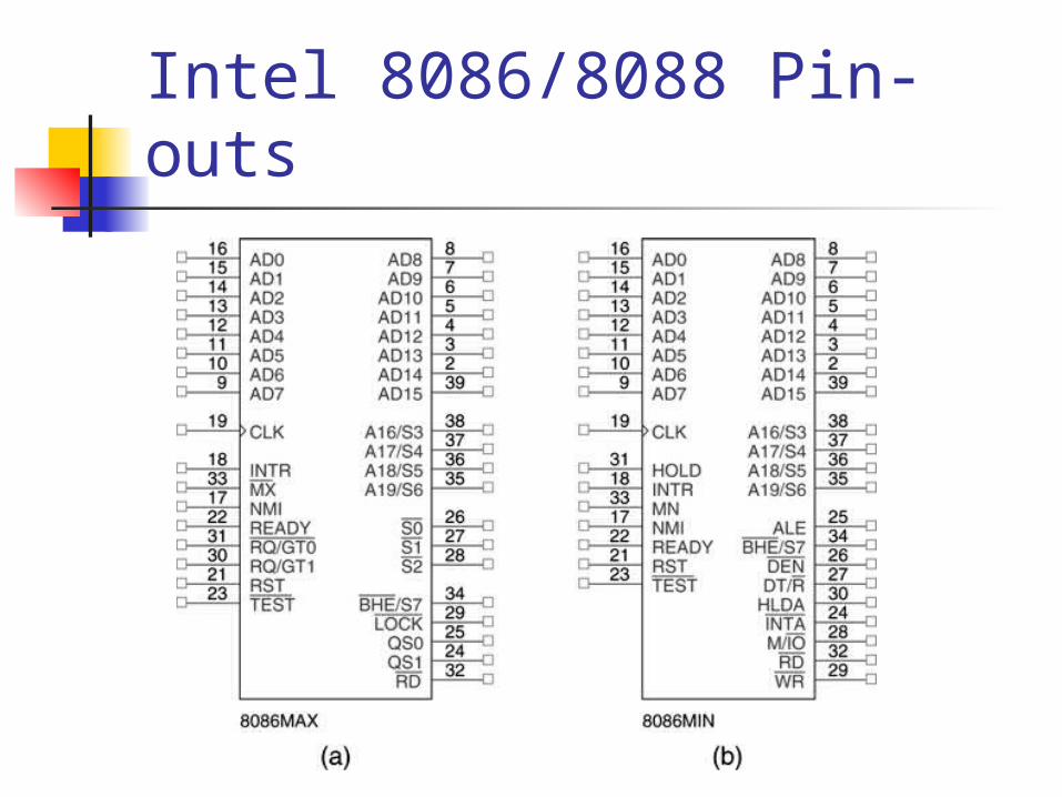
Intel 8086/8088 Pin-outs
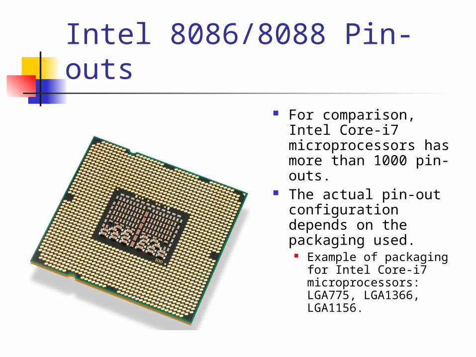
Intel 8086/8088 Pin-outs For comparison, Intel
Core-i7 microprocessors has more than 1000 pin-outs.
The actual pin-out configuration depends on the packaging used.
Example of packaging for Intel Core-i7 microprocessors: LGA775, LGA1366, LGA1156.

Intel 8086/8088 Pin-outs
AD15 – AD0
Address/data bus lines. Contains memory address or I/O port
number whenever ALE (Address Latch Enable) pin is 1.
Contains data whenever ALE is 0. A19/S6 – A16/S3
Address/status bus lines.

Intel 8086/8088 Pin-outs RD
Read signal. When RD = 0, the data bus is receptive
to data from memory or I/O devices. READY
If READY = 0, the microprocessor enters into wait state and becomes idle.
Otherwise, the microprocessor functions normally.

Intel 8086/8088 Pin-outs INTR
Interrupt request. If INTR = 1, the microprocessor enters an
interrupt acknowledge cycle after the current instruction has completed execution.
NMI Non-maskable interrupt. Similar to INTR, except that interrupt will be
executed even though the IF flag bit is 0. Interrupt vector 2 will be used to service the
interrupt.
Intel 8086/8088 Pin-outs
INTA Interrupt acknowledge. Output a response when an interrupt
signal is received on the INTR pin. Upon receiving the response, the
system circuit would then send the interrupt vector number on the data bus.
Intel 8086/8088 Pin-outs TEST
An input that is tested by the WAIT instruction.
If TEST = 0, the WAIT instruction functions as a NOP.
If TEST = 1, the WAIT instruction will wait for TEST to become 0.
This TEST pin is most often connected to the 8087 co-processor.
Intel 8086/8088 Pin-outs
RESET If RESET = 1 for four clocking periods,
the microprocessor will reset itselt. When the processor is reset, it
executes instructions at memory location FFFF0H.
CLK Connected to a clock to provide timing
signal for the microprocessor.
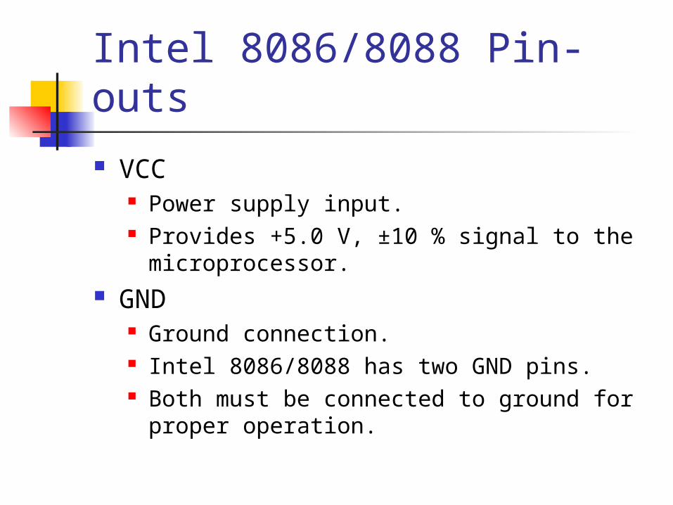
Intel 8086/8088 Pin-outs VCC
Power supply input. Provides +5.0 V, ±10 % signal to the
microprocessor. GND
Ground connection. Intel 8086/8088 has two GND pins. Both must be connected to ground for
proper operation.
Intel 8086/8088 Pin-outs
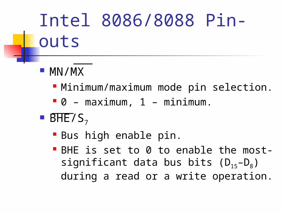
MN/MX Minimum/maximum mode pin selection. 0 – maximum, 1 – minimum.
BHE/S7
Bus high enable pin. BHE is set to 0 to enable the most-
significant data bus bits (D15–D8) during a read or a write operation.

Intel 8086/8088 Pin-outs M/IO
Selects memory or I/O. Indicates whether the address bus contains
a memory address or an I/O port address. 0 – I/O, 1 – memory.
WR Write line. Indicates whether the microprocessor is
outputting data

Intel 8086/8088 Pin-outs DT/R
Data transmit/receive. Shows whether the data bus is transmitting
or receiving. 1 – transmitting, 0 – receiving.
HOLD Request a direct memory access (DMA).
HLDA Indicates that the microprocessor has
entered a HOLD state.

Memory Pin Connections Typical pins on a
memory chip. Address
connection Data connection Selection input Control input to
select read or write operation.

Memory Pin Connections Address connections
To select memory location within the memory device.
The number of pins depend of the number of memory locations.
1K (1024) – 10 pins 1M (1048576) – 20 pins 1G (1073741824) – 30 pins 4G (4294967296) – 32 pins

Memory Pin Connections Data connections
Carries data to/from the memory device. The number of pins is determined by the data
width. Most devices are currently 8-bit wide. There are also devices with 16, 4 or 1 bit wide.
Catalog listings of memory devices often refer to memory locations times bits per location.
1K x 8 means 1K memory locations and 8-bit in each location.
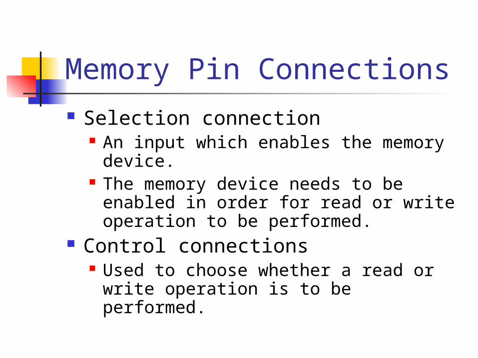
Memory Pin Connections Selection connection
An input which enables the memory device.
The memory device needs to be enabled in order for read or write operation to be performed.
Control connections Used to choose whether a read or
write operation is to be performed.
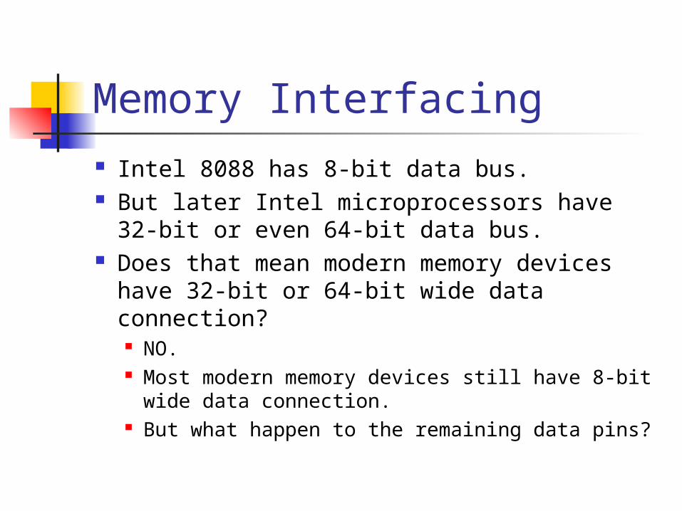
Memory Interfacing Intel 8088 has 8-bit data bus. But later Intel microprocessors have 32-bit
or even 64-bit data bus. Does that mean modern memory devices
have 32-bit or 64-bit wide data connection? NO. Most modern memory devices still have 8-bit
wide data connection. But what happen to the remaining data pins?

Memory Interfacing Processors with more than 8-bit wide
data bus can use a number of memory banks.
For example, a microprocessor with 32-bit wide data bus can use up to four 8-bit wide memory banks, each can contain 1G locations. If 32-bit number is transferred, all four banks
are selected. For 16-bit number, two banks. For 8-bit number, one bank.

Memory Interfacing

I/O Devices I/O devices allow the microprocessor to
communicate with the outside world. This is what makes the microprocessor “useful”.
Similar to memory interfacing, I/O interfacing also uses the data and address lines. Data lines are still used to send/receive data
from the I/O device. However, the address lines are used to specify
the port number, which specifies the I/O device to be accessed.

I/O Instructions There are two basic I/O instructions:
IN – to read data from I/O device OUT – to write data to I/O device
Format: IN dest, src OUT dest, src
There are also instructions INS and OUTS: Used to transfer strings of data between
memory and I/O device. Found in all Intel microprocessors except
8086 and 8088.

I/O Instructions There are two ways to specify the I/O
address in IN/OUT instructions: Fixed address
8-bit address. Address specified as an immediate value.
Variable address 16-bit address. Address is stored in DX.
The data register used for IN/OUT must always be AL, AX or EAX (depending on data length).

I/O Instructions The first 256 I/O port addresses (00H–
FFH) are accessed by both fixed and variable I/O instructions.
I/O address from 0100H to FFFFH is only accessed by the variable I/O address.
I/O ports are always 8-bit in width (i.e. the data size is 8-bit). A 16-bit port is actually two consecutive 8-
bit ports being addressed. A 32-bit port is actually four consecutive 8-
bit ports being addressed.

Types of I/O Interfacing There are two different methods of I/O
interfacing: Isolated I/O Memory-mapped I/O
Isolated I/O uses the IN, OUT, INS and OUTS instructions to transfer data to/from I/O device.
Memory mapped I/O transfer data to I/O device simply by using any instruction that references the memory.

Isolated I/O The word ‘isolated’ refers to the concept
where the I/O address space is separated from memory address space.
Access to the I/O address space must be done using IN, OUT, INS and OUTS instructions.
Control signals such as M/IO are required to indicate whether the microprocessor is accessing the memory or I/O.

Memory-mapped I/O There is only one single address space for both
memory and I/O. Memory-mapped I/O does not use the IN, OUT,
INS and OUTS instructions. It uses any instruction that transfers data
between the microprocessor and memory, such as MOV.
Advantage: simple to implement in a program. Disadvantage: it takes up a portion of the
system memory and therefore reduces the amount of memory available to applications.
This is the reason why if you install 4GB of RAM on a PC running 32-bit Windows, you cannot get the full 4GB.

Personal Computer I/O Map
This diagram shows an example of I/O map for a PC.
The I/O map shows the I/O address for different peripherals.
I/O space between ports 0000H and 03FFH is normally reserved for the system and ISA bus.
Ports at 0400H–FFFFH are generally available for user applications, main-board functions, and the PCI bus.
On Windows, you can see this by going to Control Panel System Device Manager (on Hardware tab).

Synchronizing with I/O Device Many I/O devices accept or release data
slower than the microprocessor. The microprocessor can only read/write an
I/O device when the device is ready to do so. But how can we know whether the device is
ready? There are two methods to synchronize with
I/O devices: Using interrupt Polling

Synchronizing with I/O Device If interrupt is used, the device will send an
interrupt signal to the microprocessor when it is ready.
Recall hardware interrupt discussed in Chapter 5. The interrupt service routine will then be executed to
perform the necessary operation. If polling is used, the program which performs the
I/O operation will enter a loop to keep checking whether the device is ready.
There is normally a pin connection on the device that can be read for this purpose.
The disadvantage of this is that while doing polling, the program will only do this and cannot do other tasks.

Direct Memory Access (DMA) DMA is another method of transferring data
to/from I/O devices. However, it differs from isolated and memory-
mapped I/O in the sense that the transfer is done without the use of the microprocessor.
Data transfer is done directly between memory and I/O devices.
DMA read transfers data from memory to I/O device. DMA write transfers data from I/O device to memory. This frees the microprocessor from the I/O operation
and allows it to do other work.
Direct Memory Access (DMA) With DMA, the microprocessor would only need to
initiate the DMA operation. The HOLD and HLDA pins are used for this purpose.
While the data transfer is in progress, the microprocessor can continue doing other work.
This is essential in keeping the microprocessor productive. Without the use of DMA, the microprocessor will be busy
doing the data transfer, which is a very slow operation (compared to the microprocessor’s speed).
The only operation that the microprocessor cannot do within this time is another I/O operation.
Address and data bus is blocked for DMA data transfer.

Direct Memory Access (DMA) When the data transfer is done, the
DMA controller will send an interrupt to the microprocessor.
DMA is commonly used with I/O devices that require bulk data transfer. Disk drive controllers Graphics cards Sound cards Network cards
DMA is also used for intra-chip data transfer in multi-core processors.

Bus Interface Allow external devices to be connected
to the computer’s motherboard. Consequently, allow the devices to be
accessed from software running on the computer.
There have been many bus interface technologies. Among them are: ISA (industry standard architecture) bus PCI (peripheral component interconnect) bus PCIe (PCI Express) bus AGP (advanced graphics port) USB (universal serial bus)

ISA Bus ISA bus has been around since the
beginning of IBM PC. Popularly used up until Pentium III
computers. There have been several versions:
8-bit ISA bus 16-bit ISA bus 32-bit ISA bus, also called EISA (Extended
ISA)
PCI Bus Starting from Pentium IV systems, PCI
bus has started to replace ISA. Main advantages of PCI bus over ISA:
Plug-and-play feature. Allows the computer to automatically configure
the PCI card. Done using a series of registers at the PCI
interface which contain information about the board.
Ability to function with a 64-bit data bus. Supports both 32-bit and 64-bit data bus, with 32-
bit address bus.
PCI Bus
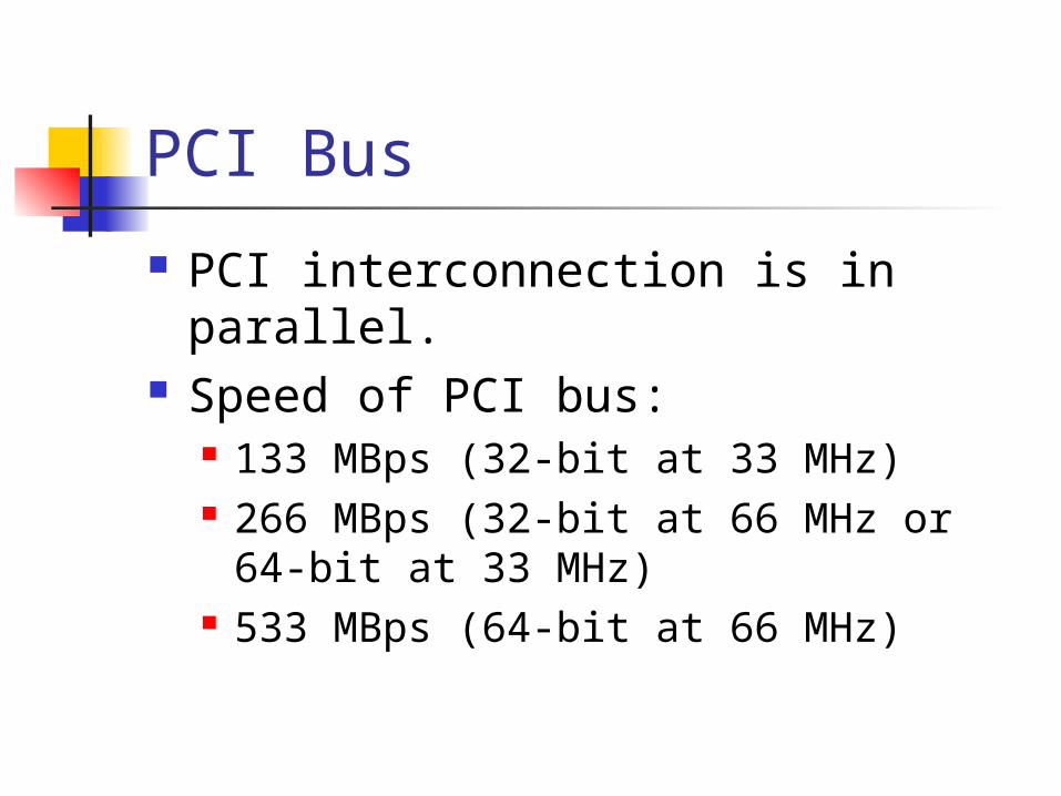
PCI interconnection is in parallel. Speed of PCI bus:
133 MBps (32-bit at 33 MHz) 266 MBps (32-bit at 66 MHz or 64-bit
at 33 MHz) 533 MBps (64-bit at 66 MHz)
AGP As graphic adapter (video card)
gets more advanced, the PCI bus is no longer adequate to transfer its data. The industry ops for AGP instead.
AGP can provide a maximum data transfer rate of 2 GBps.
However, with the arrival of PCIe, AGP is no longer used.
PCI Express Bus Offers much higher speed compared to the
PCI bus. This is achieved through:
The use of high-speed serial interconnection. Operating at a much higher speed of 2.5 GHz.
Each serial connection on the PCIe bus is called a lane. A single lane is called referred to as (x1). The PCIe standard defines slots and connectors
for multiple widths: x1, x4, x8, x16, x32.

PCI Express Bus Data link speed per lane:
PCIe 1.x: 250 MBps PCIe 2.x: 500 MBps PCIe 3.0: 1 GBps
The total data link speed would depend on the number of lanes available on the PCIe card. For example: x16 PCIe 3.0: 16 GBps
The high speed makes the PCIe bus suitable for cards which require a high speed data transfer such as a video card.

USB USB was designed to standardize the
connection of computer peripherals. External storage device, keyboard and
mouse, sound card, video cam, printer, etc. USB can even supply electric power to
devices. However USB is also used in other
electronic devices such as smartphone, media player and gaming console.
This makes USB the most used interconnection bus today.

USB USB maximum speed:
USB 1.0/1.1: 1.5 MBps (12 Mbps) USB 2.0: 60 MBps (480 Mbps) USB 3.0: 640 MBps (5 Gbps)
The later versions are backward compatible with earlier versions.
To achieve the maximum speed, both the device and the USB interface must support the same version.
Legacy I/O Ports Before the existence of USB, external
devices are connected to computers using the following ports: Serial COM ports Parallel printer interface (LPT)
Also known as parallel port. Used mainly for printers.
PS/2 ports Used for keyboard and mouse
Many new computer systems no longer have one or more of these ports installed.