CS:APP3e Web Aside ARCH:VLOG Verilog Implementation of a Pipelined...
50
CS:APP3e Web Aside ARCH:VLOG Verilog Implementation of a Pipelined Y86-64 Processor * Randal E. Bryant David R. O’Hallaron December 29, 2014 Notice The material in this document is supplementary material to the book Computer Systems, A Programmer’s Perspective, Third Edition, by Randal E. Bryant and David R. O’Hallaron, published by Prentice-Hall and copyrighted 2016. In this document, all references beginning with “CS:APP3e ” are to this book. More information about the book is available at csapp.cs.cmu.edu. This document is being made available to the public, subject to copyright provisions. You are free to copy and distribute it, but you must give attribution for any use of this material. 1 Introduction Modern logic design involves writing a textual representation of a hardware design in a hardware description language. The design can then be tested by both simulation and by a variety of formal verification tools. Once we have confidence in the design, we can use logic synthesis tools to translate the design into actual logic circuits. In this document, we describe an implementation of the PIPE processor in the Verilog hardware description language. This design combines modules implementing the basic building blocks of the processor, with control logic generated directly from the HCL description developed in CS:APP2eChapter 4 and presented in Web Aside ARCH:HCL. We have been able to synthesize this design, download the logic circuit de- scription onto field-programmable gate array (FPGA) hardware, and have the processor execute Y86-64 programs. Aside: A Brief History of Verilog Many different hardware description languages (HDLs) have been developed over the years, but Verilog was the first to achieve widespread success. It was developed originally by Philip Moorby, working at a company started in 1983 by Prabhu Goel to produce software that would assist hardware designers in designing and testing digital hardware. * Copyright c 2015, R. E. Bryant, D. R. O’Hallaron. All rights reserved. 1
Transcript of CS:APP3e Web Aside ARCH:VLOG Verilog Implementation of a Pipelined...
CS:APP3e Web Aside ARCH:VLOGVerilog Implementation of a Pipelined Y86-64 Processor∗
Randal E. BryantDavid R. O’Hallaron
December 29, 2014
Notice
The material in this document is supplementary material to the book Computer Systems, A Programmer’sPerspective, Third Edition, by Randal E. Bryant and David R. O’Hallaron, published by Prentice-Hall andcopyrighted 2016. In this document, all references beginning with “CS:APP3e ” are to this book. Moreinformation about the book is available at csapp.cs.cmu.edu.
This document is being made available to the public, subject to copyright provisions. You are free to copyand distribute it, but you must give attribution for any use of this material.
1 Introduction
Modern logic design involves writing a textual representation of a hardware design in a hardware descriptionlanguage. The design can then be tested by both simulation and by a variety of formal verification tools.Once we have confidence in the design, we can use logic synthesis tools to translate the design into actuallogic circuits.
In this document, we describe an implementation of the PIPE processor in the Verilog hardware descriptionlanguage. This design combines modules implementing the basic building blocks of the processor, withcontrol logic generated directly from the HCL description developed in CS:APP2eChapter 4 and presentedin Web Aside ARCH:HCL. We have been able to synthesize this design, download the logic circuit de-scription onto field-programmable gate array (FPGA) hardware, and have the processor execute Y86-64programs.
Aside: A Brief History of VerilogMany different hardware description languages (HDLs) have been developed over the years, but Verilog was the firstto achieve widespread success. It was developed originally by Philip Moorby, working at a company started in 1983by Prabhu Goel to produce software that would assist hardware designers in designing and testing digital hardware.
∗Copyright c© 2015, R. E. Bryant, D. R. O’Hallaron. All rights reserved.
1
2
They gave their company what seemed at the time like a clever name: Automated Integrated Design Systems,or “AIDS.” When that acronym became better known to stand for Acquired Immune Deficiency Syndrome, theyrenamed their company Gateway Design Automation in 1985. Gateway was acquired by Cadence Design Systemsin 1990, which remains one of the major companies in Electronic Design Automation (EDA). Cadence transferredthe Verilog language into the public domain, and it became IEEE Standard 1364-1995. Since then it has undergoneseveral revisions, as well.
Verilog was originally conceived as a language for writing simulation models for hardware. The task of designingactual hardware was still done by more manual means of drawing logic schematics, with some assistance providedby software for drawing circuits on a computer.
Starting in the 1980s, researchers developed efficient means of automatically synthesizing logic circuits from moreabstract descriptions. Given the popularity of Verilog for writing simulation models, it was natural to use thislanguage as the basis for synthesis tools. The first, and still most widely used such tool is the Design Compiler,marked by Synopsys, Inc., another major EDA company. End Aside.
Since Verilog was originally designed to create simulation models, it has many features that cannot besynthesized into hardware. For example, it is possible to describe the detailed timing of different events,whereas this would depend greatly on the hardware technology for which the design is synthesized. Asa result, there is a recognized synthesizable subset of the Verilog language, and hardware designers mustrestrict how they write Verilog descriptions to ensure they can be synthesized. Our Verilog stays well withinthe bounds of the synthesizable subset.
This document is not intended to be a complete description of Verilog, but just to convey enough about itto see how we can readily translate our Y86-64 processor designs into actual hardware. A comprehensivedescription of Verilog is provided by Thomas and Moorby’s book [1]
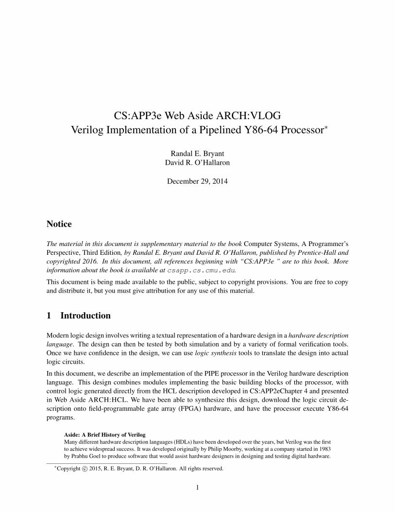
A complete Verilog implementation of PIPE suitable for logic synthesis is given in Appendix A of thisdocument. We will go through some parts of this description, using the fetch stage of the PIPE processor asour main source of examples. For reference, a diagram of this stage is shown in Figure 1.
2 Combinational Logic
The basic data type for Verilog is the bit vector, a collection of bits having a range of indices. The standardnotation for bit vectors is to specify the indices as a range of the form [hi:lo], where integers hi and logive the index values of the most and least significant bits, respectively. Here are some examples of signaldeclarations:
wire [63:0] aluA;wire [ 3:0] alufun;wire stall;
These declarations specify that the signals are of type wire, indicating that they serve as connections in acombinational circuit, rather than storing any information. We see that signals aluA and alufun are vectorsof 64 and 4 bits, respectively, and that stall is a single bit (indicated when no index range is given.)
The operations on Verilog bit vectors are similar to those on C integers: arithmetic and bit-wise operations,shifting, and testing for equality or ordering relationships. In addition, it is possible to create new bit vectorsby extracting ranges of bits from other vectors. For example, the expression aluA[63:56] creates an8-bit wide vector equal to the most significant byte of aluA.

3
F
D rB
M_icode
PredictPC
valC valPicode ifun rA
Instructionmemory
PCincrement
predPC
Needregids
NeedvalC
Instrvalid
AlignSplit
Bytes 1-9Byte 0
SelectPC
M_BchM_valA
W_icodeW_valM
f_pc
stat
stat
imem_error
icode ifun
Figure 1: PIPE PC selection and fetch logic.

4
// Split instruction byte into icode and ifun fieldsmodule split(ibyte, icode, ifun);
input [7:0] ibyte;output [3:0] icode;output [3:0] ifun;
assign icode = ibyte[7:4];assign ifun = ibyte[3:0];
endmodule
// Extract immediate word from 9 bytes of instructionmodule align(ibytes, need_regids, rA, rB, valC);
input [71:0] ibytes;input need_regids;output [ 3:0] rA;output [ 3:0] rB;output [63:0] valC;assign rA = ibytes[7:4];assign rB = ibytes[3:0];assign valC = need_regids ? ibytes[71:8] : ibytes[63:0];
endmodule
// PC incrementermodule pc_increment(pc, need_regids, need_valC, valP);
input [63:0] pc;input need_regids;input need_valC;output [63:0] valP;assign valP = pc + 1 + 8*need_valC + need_regids;
endmodule
Figure 2: Hardware Units for Fetch Stage. These illustrate the use of modules and bit vector operationsin Verilog.
Verilog allows a system to be described as a hierarchy of modules. These modules are similar to procedures,except that they do not define an action to be performed when invoked, but rather they describe a portion ofa system that can be instantiated as a block of hardware. Each module declares a set of interface signals—the inputs and outputs of the block—and a set of interconnected hardware components, consisting of eitherother module instantiations or primitive logic operations.
As an example of Verilog modules implementing simple combinational logic, Figure 2 shows Verilog de-scriptions of the hardware units required by the fetch stage of PIPE. For example, the module split servesto split the first byte of an instruction into the instruction code and function fields. We see that this modulehas a single eight-bit input ibyte and two four-bit outputs icode and ifun. Output icode is defined to be thehigh-order four bits of ibyte, while ifun is defined to be the low-order four bits.
Verilog has several different forms of assignment operators. An assignment starting with the keywordassign is known as a continuous assignment. It can be thought of as a way to connect two signals via

5
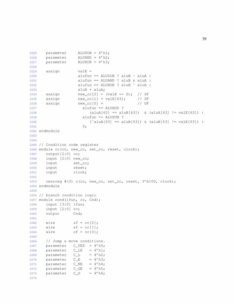
module alu(aluA, aluB, alufun, valE, new_cc);input [63:0] aluA, aluB; // Data inputsinput [ 3:0] alufun; // ALU functionoutput [63:0] valE; // Data Outputoutput [ 2:0] new_cc; // New values for ZF, SF, OF
parameter ALUADD = 4’h0;parameter ALUSUB = 4’h1;parameter ALUAND = 4’h2;parameter ALUXOR = 4’h3;
assign valE =alufun == ALUSUB ? aluB - aluA :alufun == ALUAND ? aluB & aluA :alufun == ALUXOR ? aluB ˆ aluA :aluB + aluA;
assign new_cc[2] = (valE == 0); // ZFassign new_cc[1] = valE[63]; // SFassign new_cc[0] = // OF
alufun == ALUADD ?(aluA[63] == aluB[63]) & (aluA[63] != valE[63]) :
alufun == ALUSUB ?(˜aluA[63] == aluB[63]) & (aluB[63] != valE[63]) :
0;endmodule
Figure 3: Verilog implementation of Y86-64 ALU. This illustrates arithmetic and logical operations, aswell as the Verilog notation for bit-vector constants.
simple wires, as when constructing combinational logic. Unlike an assignment in a programming languagesuch as C, continuous assignment does not specify a single updating of a value, but rather it creates apermanent connection from the output of one block of logic to the input of another. So, for example, thedescription in the split module states that the two outputs are directly connected to the relevant fields ofthe input.
The align module describes how the processor extracts the remaining fields from an instruction, de-pending on whether or not the instruction has a register specifier byte. Again we see the use of contin-uous assignments and bit vector subranges. This module also includes a conditional expression, similarto the conditional expressions of C. In Verilog, however, this expression provides a way of creating amultiplexor—combinational logic that chooses between two data inputs based on a one-bit control signal.
The pc increment module demonstrates some arithmetic operations in Verilog. These are similar to thearithmetic operations of C. Originally, Verilog only supported unsigned arithmetic on bit vectors. Two’scomplement arithmetic was introduced in the 2001 revision of the language. All operations in our descrip-tion involve unsigned arithmetic.
As another example of combinational logic, Figure 3 shows an implementation of an ALU for the Y86-64execute stage. We see that it has as inputs two 64-bit data words and a 4-bit function code. For outputs,

6
// Clocked register with enable signal and synchronous reset// Default width is 8, but can be overridenmodule cenrreg(out, in, enable, reset, resetval, clock);
parameter width = 8;output [width-1:0] out;reg [width-1:0] out;input [width-1:0] in;input enable;input reset;input [width-1:0] resetval;input clock;
always@(posedge clock)begin
if (reset)out <= resetval;
else if (enable)out <= in;
endendmodule
Figure 4: Basic Clocked Register.
it has a 64-bit data word and the three bits used to create condition codes. The parameter statementprovides a way to give names to constant values, much as the way constants can be defined in C using#define. In Verilog, a bit-vector constant has a specific width, and a value given in either decimal (thedefault), hexadecimal (specified with ‘h’), or binary (specified with ‘b’) form. For example, the notation4’h2 indicates a 4-bit wide vector having hexadecimal value 0x2. The rest of the module describes thefunctionality of the ALU. We see that the data output will equal the sum, difference, bitwise EXCLUSIVE-OR, or bitwise AND of the two data inputs. The output conditions are computed using the values of the inputand output data words, based on the properties of a two’s complement representation of the data (CS:APP3eSection 2.3.2.)
3 Registers
Thus far, we have considered only combinational logic, expressed using continuous assignments. Veriloghas many different ways to express sequential behavior, event sequencing, and time-based waveforms. Wewill restrict our presentation to ways to express the simple clocking methods required by the Y86-64 pro-cessor.
Figure 4 shows a clocked register cenrreg (short for “conditionally-enabled, resettable register”) that wewill use as a building block for the hardware registers in our processor. The idea is to have a register that canbe loaded with the value on its input in response to a clock. Additionally, it is possible to reset the register,causing it to be set to a fixed constant value.
7
Some features of this module are worth highlighting. First, we see that the module is parameterized by avalue width, indicating the number of bits comprising the input and output words. By default, the modulehas a width of 8 bits, but this can be overridden by instantiating the module with a different width.
We see that the register data output out is declared to be of type reg (short for “register”). That means thatit will hold its value until it is explicitly updated. This contrasts to the signals of type wire that are used toimplement combinational logic.
The statement beginning always @(posedge clock) describes a set of actions that will be triggeredevery time the clock signal goes for 0 to 1 (this is considered to be the positive edge of a clock signal.)Within this statement, we see that the output may be updated to be either its input or its reset value. Theassignment operator <= is known as a non-blocking assignment. That means that the actual updating of theoutput will only take place when a new event is triggered, in this case the transition of the clock from 0 to1. We can see that the output may be updated as the clock rises. Observe, however, that if neither the resetnor the enable signals are 1, then the output will remain at its current value.
The following module preg shows how we can use our basic register to construct a pipeline register:
// Pipeline register. Uses reset signal to inject bubble// When bubbling, must specify value that will be loadedmodule preg(out, in, stall, bubble, bubbleval, clock);
parameter width = 8;output [width-1:0] out;input [width-1:0] in;input stall, bubble;input [width-1:0] bubbleval;input clock;
cenrreg #(width) r(out, in, ˜stall, bubble, bubbleval, clock);endmodule
We see that a pipeline register is created by instantiating a clocked register, but making the enable signal bethe complement of the stall signal. We see here also the way modules are instantiated in Verilog. A moduleinstantiatioin gives the name of the module, an optional list of parametric values, (in this case, we want thewidth of the register to be the width specified by the module’s parameter), an instance name (used whendebugging a design by simulation), and a list of module parameters.
The register file is implemented using 15 clocked registers for the 15 program registers. Combinational logicis used to select which program register values are routed to the register file outputs, and which programregisters to update by a write operation. The Verilog code for this is found in Appendix A, lines 135–271.
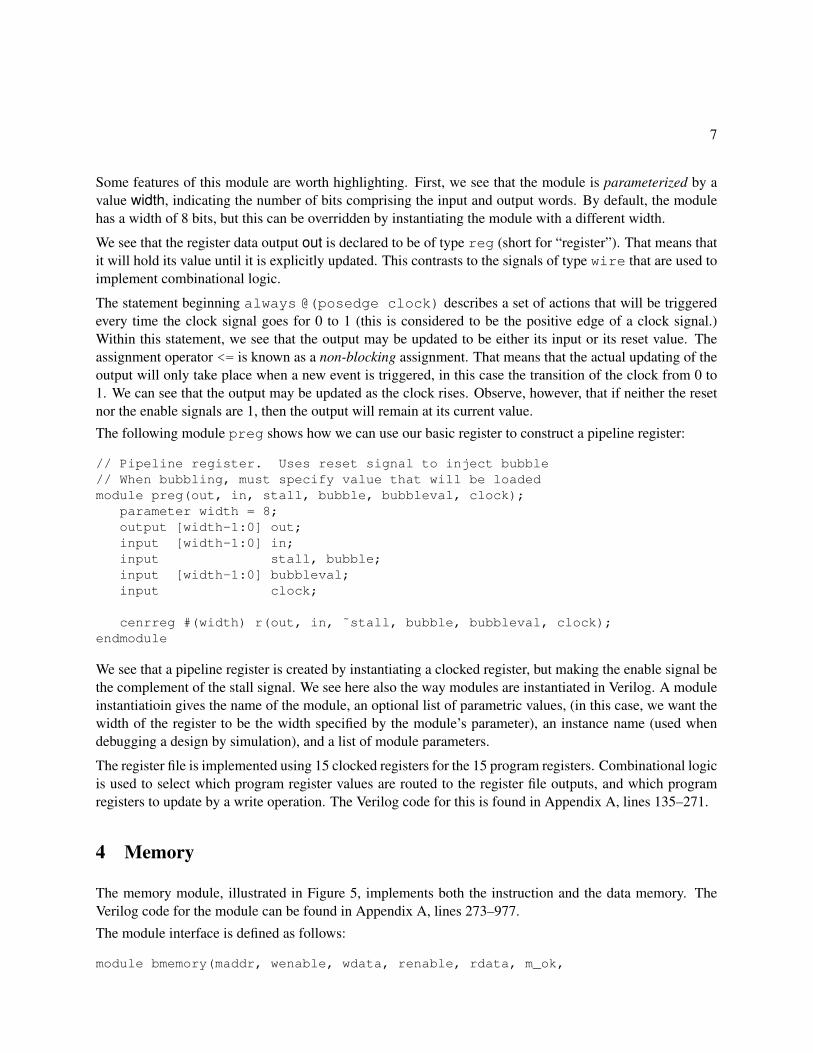
4 Memory
The memory module, illustrated in Figure 5, implements both the instruction and the data memory. TheVerilog code for the module can be found in Appendix A, lines 273–977.
The module interface is defined as follows:
module bmemory(maddr, wenable, wdata, renable, rdata, m_ok,

8
Bank 0
Bank 1
Bank 2
Bank 3
Bank 4
Bank 5
Bank 6
Bank 7
clock
maddr[63:0]wenablerenable
rdata[63:0]
wdata[63:0]
m_ok
iaddr[63:0]
idata[79:0]
i_ok
Bank 8
Bank 9
Bank A
Bank B
Bank C
Bank D
Bank E
Bank F
Figure 5: Memory structure. The memory consists of 16 banks, each performing single-byte reads andwrites.

9
iaddr, instr, i_ok, clock);parameter memsize = 8192; // Number of bytes in memoryinput [63:0] maddr; // Read/Write addressinput wenable; // Write enableinput [63:0] wdata; // Write datainput renable; // Read enableoutput [63:0] rdata; // Read dataoutput m_ok; // Read & write addresses within rangeinput [63:0] iaddr; // Instruction addressoutput [79:0] instr; // 10 bytes of instructionoutput i_ok; // Instruction address within rangeinput clock;
In Figure 5, we adopt the Verilog convention of indicating the index ranges for each of the multi-bit signals.The left-hand side of the figure shows the port used for reading and writing data. We see that it has anaddress input maddr, data output rdata and input wdata, and enable signals for reading and writing. Theoutput signal m ok indicates whether or not the address input is within the range of valid addresses for thememory.
The right-hand side of the figure shows the port used for fetching instructions. It has just an address inputiaddr, an 80-byte wide data output idata, and a signal i ok indicating whether or not the address is withinthe range of valid addresses.
We require a method for accessing groups of 8 or 10 successive bytes in the memory, and we cannot assumeany particular alignment for the addresses. We therefore implement the memory with a set of 16 banks, eachof which is a random-access memory that can be used to store, read, and write individual bytes. A byte withmemory address i is stored in bank i mod 16, and the address of the byte within the bank is bi/16c. Someadvantages of this organization are:
• Any 10 successive bytes will be stored in separate banks. Thus, the processor can read all 10 instruc-tion bytes using single-byte bank reads. Similarly, the processor can read or write all 8 data bytesusing single-byte bank reads or writes.
• The bank number is given by the low-order 4 bits of the memory address.
• The address of a byte within the bank is given by the remaining bits of the memory address.
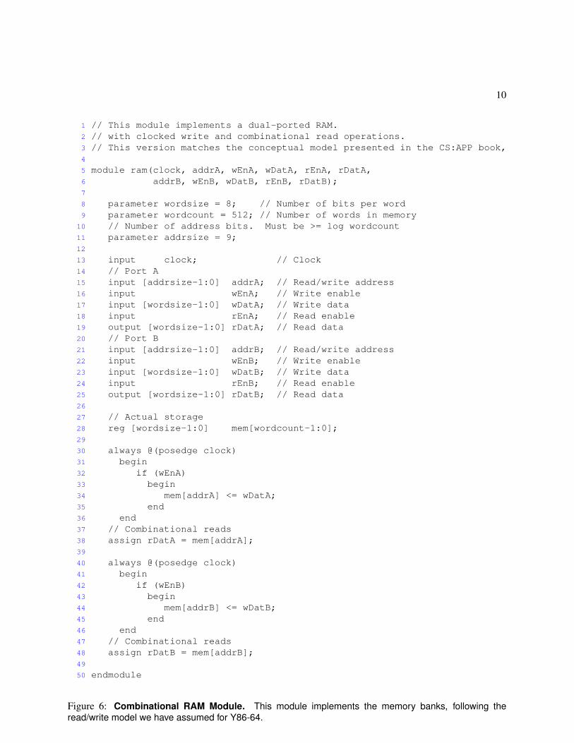
Figure 6 gives a Verilog description of a combinational RAM module suitable for implementing the memorybanks. This RAM stores data in units of words, where we set the word size to be eight bits. We see that themodule has three associated parametric values:
wordsize: The number of bits in each word of the memory. The default value is eight.
wordcount: The number of words stored in the memory. The default value of 512 creates a memorycapable of storing 16 · 512 = 8192 bytes.
addrsize: The number of bits in the address input. If the memory contains n words, this parameter mustbe at least log2 n.
10
1 // This module implements a dual-ported RAM.2 // with clocked write and combinational read operations.3 // This version matches the conceptual model presented in the CS:APP book,4
5 module ram(clock, addrA, wEnA, wDatA, rEnA, rDatA,6 addrB, wEnB, wDatB, rEnB, rDatB);7
8 parameter wordsize = 8; // Number of bits per word9 parameter wordcount = 512; // Number of words in memory10 // Number of address bits. Must be >= log wordcount11 parameter addrsize = 9;12
13 input clock; // Clock14 // Port A15 input [addrsize-1:0] addrA; // Read/write address16 input wEnA; // Write enable17 input [wordsize-1:0] wDatA; // Write data18 input rEnA; // Read enable19 output [wordsize-1:0] rDatA; // Read data20 // Port B21 input [addrsize-1:0] addrB; // Read/write address22 input wEnB; // Write enable23 input [wordsize-1:0] wDatB; // Write data24 input rEnB; // Read enable25 output [wordsize-1:0] rDatB; // Read data26
27 // Actual storage28 reg [wordsize-1:0] mem[wordcount-1:0];29
30 always @(posedge clock)31 begin32 if (wEnA)33 begin34 mem[addrA] <= wDatA;35 end36 end37 // Combinational reads38 assign rDatA = mem[addrA];39
40 always @(posedge clock)41 begin42 if (wEnB)43 begin44 mem[addrB] <= wDatB;45 end46 end47 // Combinational reads48 assign rDatB = mem[addrB];49
50 endmodule
Figure 6: Combinational RAM Module. This module implements the memory banks, following theread/write model we have assumed for Y86-64.

11
Comb logic I Comb. logic II
Clock
update registers
read & update memories
update registers
Figure 7: Timing of synchronous RAM. By having the memory be read and written on the falling clockedge, the combinational logic can be active both before (A) and after (B) the memory operation.
This module implements the model we have assumed in Chapter 4: memory writes occur when the clockgoes high, but memory reads operate as if the memory were a block of combinational logic.
Several features of the combinational RAM module are worth noting. We see the declaration of the actualmemory array on line 28. It declares mem to be an array with elements numbered from 0 to the word countminus 1, where each array element is a bit vector with bits numbered from 0 to the word size minus 1.Furthermore, each bit is of type reg, and therefore acts as a storage element.
The combinational RAM has two ports, labeled “A” and “B,” that can be independently written on eachcycle. We see the writes occurring within always blocks, and each involving a nonblocking assignment(lines 34 and 44.) The memory array is addressed using an array notation. We see also the two reads areexpressed as continuous assignments (lines 38 and 48), meaning that these outputs will track the values ofwhatever memory elements are being addressed.
The combinational RAM is fine for running simulations of the processor using a Verilog simulator. In reallife, however, most random-access memories require a clock to trigger a sequence of events that carriesout a read operation (see CS:APP3e Section 6.1.1), and so we must modify our design slightly to workwith a synchronous RAM, meaning that both read and write operations occur in response to a clock signal.Fortunately, a simple timing trick allows us to use a synchronous RAM module in the PIPE processor.
We design the RAM blocks used to implement the memory banks, such that the read and write operations aretriggered by the falling edge of the clock, as it makes the transition for 1 to 0. This yields a timing illustratedin Figure 7. We see that the regular registers (including the pipeline registers, the condition code register,and the register file) are updated when the clock goes from 0 to 1. At this point, values propagate throughcombinational logic to the address, data, and control inputs of the memory. The clock transition from 1 to0 causes the designated memory operations to take place. More combinational logic is then activated topropagate values to the register inputs, arriving there in time for the next clock transition.
With this timing, we can therefore classify each combinational logic block as being either in group I, mean-ing that it depends only on the values stored in registers, and group II, meaning that it depends on the valuesread from memory.
Practice Problem 1:
Determine which combination logic blocks in the fetch stage (Figure 1) are in group I, and which are ingroup II.

12
1 // This module implements a dual-ported RAM.2 // with clocked write and read operations.3
4 module ram(clock, addrA, wEnA, wDatA, rEnA, rDatA,5 addrB, wEnB, wDatB, rEnB, rDatB);6
7 parameter wordsize = 8; // Number of bits per word8 parameter wordcount = 512; // Number of words in memory9 // Number of address bits. Must be >= log wordcount10 parameter addrsize = 9;11
12
13 input clock; // Clock14 // Port A15 input [addrsize-1:0] addrA; // Read/write address16 input wEnA; // Write enable17 input [wordsize-1:0] wDatA; // Write data18 input rEnA; // Read enable19 output [wordsize-1:0] rDatA; // Read data20 reg [wordsize-1:0] rDatA;21 // Port B22 input [addrsize-1:0] addrB; // Read/write address23 input wEnB; // Write enable24 input [wordsize-1:0] wDatB; // Write data25 input rEnB; // Read enable26 output [wordsize-1:0] rDatB; // Read data27 reg [wordsize-1:0] rDatB;28
29 reg[wordsize-1:0] mem[wordcount-1:0]; // Actual storage30
31 always @(negedge clock)32 begin33 if (wEnA)34 begin35 mem[addrA] <= wDatA;36 end37 if (rEnA)38 rDatA <= mem[addrA];39 end40
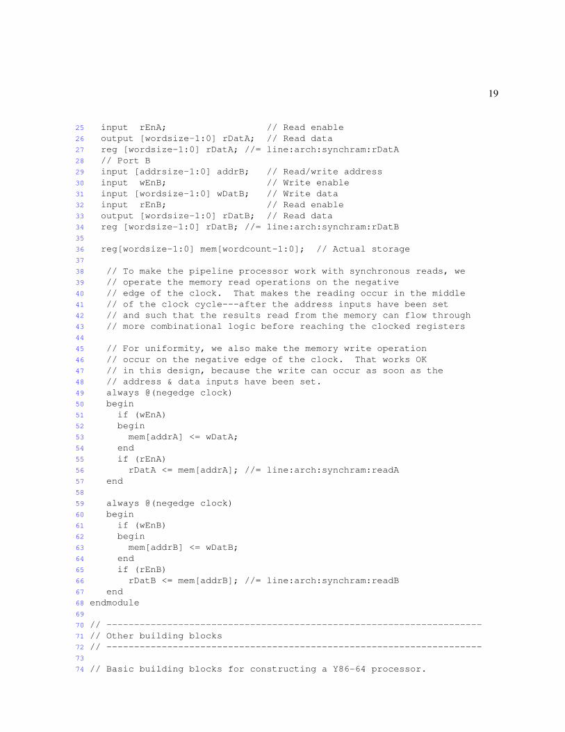
41 always @(negedge clock)42 begin43 if (wEnB)44 begin45 mem[addrB] <= wDatB;46 end47 if (rEnB)48 rDatB <= mem[addrB];49 end50 endmodule
Figure 8: Synchronous RAM Module. This module implements the memory banks using synchronousread operations.

13
Processor
clock
udaddr[63:0]
odata[63:0]
idata[63:0]
mode[2:0]
stat[2:0]
Figure 9: Processor interface. Mechanisms are included to upload and download memory data andprocessor state, and to operate the processor in different modes.
module processor(mode, udaddr, idata, odata, stat, clock);input [ 2:0] mode; // Signal operating mode to processorinput [63:0] udaddr; // Upload/download addressinput [63:0] idata; // Download data wordoutput [63:0] odata; // Upload data wordoutput [ 2:0] stat; // Statusinput clock; // Clock input
Figure 10: Declaration of processor module.
Figure 8 shows a synchronous RAM module that better reflects the random-access memories available tohardware designers. Comparing this module to the combinational RAM (Figure 6), we see two differences.First the data outputs rDatA and rDatB are both declared to be of type reg, meaning that they will hold thevalue assigned to them until they are explicitly updated (lines 20 and 27.) Second, the updating of these twooutputs occur via nonblocking assignments within always blocks (lines 38 and 48).
The remaining portions of the memory module are implemented as combinational logic, and so changingthe underlying bank memory design is the only modification required to shift the memory from havingcombinational read operations to having synchronous ones. This is the only modification required to ourprocessor design to make it synthesizable as actual hardware.
5 Overall Processor Design
We have now created the basic building blocks for a Y86-64 processor. We are ready to assemble thesepieces into an actual processor. Figure 9 shows the input and output connections we will design for ourprocessor, allowing the processor to be operated by an external controller. The Verilog declaration for theprocessor module is shown in Figure 10. The mode input specifies what the processor should be doing.The possible values (declared as parameters in the Verilog code) are
RUN: Execute instructions in the normal manner.
RESET: All registers are set to their initial values, clearing the pipeline registers and setting the program

14
counter to 0.
DOWNLOAD: The processor memory can be loaded using the udaddr address input and the idata datainput to specify addresses and values. By this means, we can load a program into the processor.
UPLOAD: Data can be extracted from the processor memory, using the address input udaddr to specifyan address and the odata output to provide the data stored at that address.
STATUS: Similar to UPLOAD mode, except that the values of the program registers, and the conditioncodes can be extracted. Each program register and the condition codes have associated addresses forthis operation.
The stat output is a copy of the Stat signal generated by the processor.
A typical operation of the processor involves the following sequence: 1) first, a program is downloaded intomemory, downloading 8 bytes per cycle in DOWNLOAD mode. The processor is then put into RESETmode for one clock cycle. The processor is operated in RUN mode until the stat output indicates that sometype of exception has occurred (normally when the processor executes a halt instruction.) The results arethen read from the processor over multiple cycles using the UPLOAD and STATUS modes.
6 Implementation Highlights
The following are samples of the Verilog code for our implementation of PIPE, showing the implementationof the fetch stage.
The following are declarations of the internal signals of the fetch stage. They are all of type wire, meaningthat they are simply connectors from one logic block to another.
wire [63:0] f_predPC, F_predPC, f_pc;wire f_ok;wire imem_error;wire [ 2:0] f_stat;wire [79:0] f_instr;wire [ 3:0] imem_icode;wire [ 3:0] imem_ifun;wire [ 3:0] f_icode;wire [ 3:0] f_ifun;wire [ 3:0] f_rA;wire [ 3:0] f_rB;wire [63:0] f_valC;wire [63:0] f_valP;wire need_regids;wire need_valC;wire instr_valid;wire F_stall, F_bubble;
The following signals must be included to allow pipeline registers F and D to be reset when either theprocessor is in RESET mode or the bubble signal is set for the pipeline register.
15
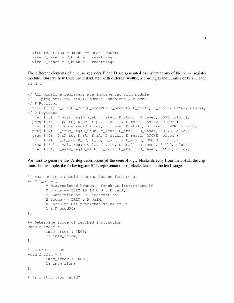
wire resetting = (mode == RESET_MODE);wire F_reset = F_bubble | resetting;wire D_reset = D_bubble | resetting;
The different elements of pipeline registers F and D are generated as instantiations of the preg registermodule. Observe how these are instantiated with different widths, according to the number of bits in eachelement:
// All pipeline registers are implemented with module// preg(out, in, stall, bubble, bubbleval, clock)// F Register
preg #(64) F_predPC_reg(F_predPC, f_predPC, F_stall, F_reset, 64’b0, clock);// D Register
preg #(3) D_stat_reg(D_stat, f_stat, D_stall, D_reset, SBUB, clock);preg #(64) D_pc_reg(D_pc, f_pc, D_stall, D_reset, 64’b0, clock);preg #(4) D_icode_reg(D_icode, f_icode, D_stall, D_reset, INOP, clock);preg #(4) D_ifun_reg(D_ifun, f_ifun, D_stall, D_reset, FNONE, clock);preg #(4) D_rA_reg(D_rA, f_rA, D_stall, D_reset, RNONE, clock);preg #(4) D_rB_reg(D_rB, f_rB, D_stall, D_reset, RNONE, clock);preg #(64) D_valC_reg(D_valC, f_valC, D_stall, D_reset, 64’b0, clock);preg #(64) D_valP_reg(D_valP, f_valP, D_stall, D_reset, 64’b0, clock);
We want to generate the Verilog descriptions of the control logic blocks directly from their HCL descrip-tions. For example, the following are HCL representations of blocks found in the fetch stage:
## What address should instruction be fetched atword f_pc = [
# Mispredicted branch. Fetch at incremented PCM_icode == IJXX && !M_Cnd : M_valA;# Completion of RET instructionW_icode == IRET : W_valM;# Default: Use predicted value of PC1 : F_predPC;
];
## Determine icode of fetched instructionword f_icode = [
imem_error : INOP;1: imem_icode;
];
# Determine ifunword f_ifun = [
imem_error : FNONE;1: imem_ifun;
];
# Is instruction valid?

16
bool instr_valid = f_icode in{ INOP, IHALT, IRRMOVQ, IIRMOVQ, IRMMOVQ, IMRMOVQ,
IOPQ, IJXX, ICALL, IRET, IPUSHQ, IPOPQ };
# Determine status code for fetched instructionword f_stat = [
imem_error: SADR;!instr_valid : SINS;f_icode == IHALT : SHLT;1 : SAOK;
];
# Does fetched instruction require a regid byte?bool need_regids =
f_icode in { IRRMOVQ, IOPQ, IPUSHQ, IPOPQ,IIRMOVQ, IRMMOVQ, IMRMOVQ };
# Does fetched instruction require a constant word?bool need_valC =
f_icode in { IIRMOVQ, IRMMOVQ, IMRMOVQ, IJXX, ICALL };
# Predict next value of PCword f_predPC = [
f_icode in { IJXX, ICALL } : f_valC;1 : f_valP;
];
We have implemented a program HCL2V (short for “HCL to Verilog”) to generate Verilog code from HCLexpressions. The following are examples of code generated from the HCL descriptions of blocks found inthe fetch stage. These are not formatted in a way that makes them easily readable, but it can be seen that theconversion from HCL to Verilog is fairly straightforward:
assign f_pc =(((M_icode == IJXX) & ˜M_Cnd) ? M_valA : (W_icode == IRET) ? W_valM :
F_predPC);
assign f_icode =(imem_error ? INOP : imem_icode);
assign f_ifun =(imem_error ? FNONE : imem_ifun);
assign instr_valid =(f_icode == INOP | f_icode == IHALT | f_icode == IRRMOVQ | f_icode ==
IIRMOVQ | f_icode == IRMMOVQ | f_icode == IMRMOVQ | f_icode == IOPQ| f_icode == IJXX | f_icode == ICALL | f_icode == IRET | f_icode ==IPUSHQ | f_icode == IPOPQ);
assign f_stat =

17
(imem_error ? SADR : ˜instr_valid ? SINS : (f_icode == IHALT) ? SHLT :SAOK);
assign need_regids =(f_icode == IRRMOVQ | f_icode == IOPQ | f_icode == IPUSHQ | f_icode ==
IPOPQ | f_icode == IIRMOVQ | f_icode == IRMMOVQ | f_icode == IMRMOVQ);
assign need_valC =(f_icode == IIRMOVQ | f_icode == IRMMOVQ | f_icode == IMRMOVQ | f_icode
== IJXX | f_icode == ICALL);
assign f_predPC =((f_icode == IJXX | f_icode == ICALL) ? f_valC : f_valP);
Finally, we must instantiate the different modules implementing the hardware units we examined earlier:
split split(f_instr[7:0], imem_icode, imem_ifun);align align(f_instr[79:8], need_regids, f_rA, f_rB, f_valC);pc_increment pci(f_pc, need_regids, need_valC, f_valP);
7 Summary
We have successfully generated a synthesizable Verilog description of a pipelined Y86-64 processor. Wesee from this exercise that the processor design we created in CS:APP3e Chapter 4 is sufficiently completethat it leads directly to a hardware realization. We have successfully run this Verilog through synthesis toolsand mapped the design onto FPGA-based hardware.
Homework Problems
Homework Problem 2 ���:
Generate a Verilog description of the SEQ processor suitable for simulation. You can use the same blocksas shown here for the PIPE processor, and you can generate the control logic from the HCL representationusing the HCL2V program. Use the combinational RAM module (Figure 6) to implement the memory banks.
Homework Problem 3 ��:
Suppose we wish to create a synthesizable version of the SEQ processor.
A. Analyze what would happen if you were to use the synchronous RAM module (Figure 8) in an im-plementation of the SEQ processor (Problem 2.)
B. Devise and implement (in Verilog) a clocking scheme for the registers and the memory banks thatwould enable the use of a synchronous RAM in an implementation of the SEQ processor.

18
Problem Solutions
Problem 1 Solution: [Pg. 11]
We see that only the PC selection block is in group I. All others depend, in part, on the value read from theinstruction memory and therefore are in group II.
Acknowledgments
James Hoe of Carnegie Mellon University has been instrumental in the design of the Y86-64 processor, inhelping us learn Verilog, and in using synthesis tools to generate a working microprocessor.
A Complete Verilog for PIPE
The following is a complete Verilog description of our implementation of PIPE. It was generated by com-bining a number of different module descriptions, and incorporating logic generated automatically from theHCL description. This model uses the synchronous RAM module suitable for both simulation and synthesis.
1 // --------------------------------------------------------------------2 // Verilog representation of PIPE processor3 // --------------------------------------------------------------------4
5 // --------------------------------------------------------------------6 // Memory module for implementing bank memories7 // --------------------------------------------------------------------8 // This module implements a dual-ported RAM.9 // with clocked write and read operations.10
11 module ram(clock, addrA, wEnA, wDatA, rEnA, rDatA,12 addrB, wEnB, wDatB, rEnB, rDatB);13
14 parameter wordsize = 8; // Number of bits per word15 parameter wordcount = 512; // Number of words in memory16 // Number of address bits. Must be >= log wordcount17 parameter addrsize = 9;18
19
20 input clock; // Clock21 // Port A22 input [addrsize-1:0] addrA; // Read/write address23 input wEnA; // Write enable24 input [wordsize-1:0] wDatA; // Write data
19
25 input rEnA; // Read enable26 output [wordsize-1:0] rDatA; // Read data27 reg [wordsize-1:0] rDatA; //= line:arch:synchram:rDatA28 // Port B29 input [addrsize-1:0] addrB; // Read/write address30 input wEnB; // Write enable31 input [wordsize-1:0] wDatB; // Write data32 input rEnB; // Read enable33 output [wordsize-1:0] rDatB; // Read data34 reg [wordsize-1:0] rDatB; //= line:arch:synchram:rDatB35
36 reg[wordsize-1:0] mem[wordcount-1:0]; // Actual storage37
38 // To make the pipeline processor work with synchronous reads, we39 // operate the memory read operations on the negative40 // edge of the clock. That makes the reading occur in the middle41 // of the clock cycle---after the address inputs have been set42 // and such that the results read from the memory can flow through43 // more combinational logic before reaching the clocked registers44
45 // For uniformity, we also make the memory write operation46 // occur on the negative edge of the clock. That works OK47 // in this design, because the write can occur as soon as the48 // address & data inputs have been set.49 always @(negedge clock)50 begin51 if (wEnA)52 begin53 mem[addrA] <= wDatA;54 end55 if (rEnA)56 rDatA <= mem[addrA]; //= line:arch:synchram:readA57 end58
59 always @(negedge clock)60 begin61 if (wEnB)62 begin63 mem[addrB] <= wDatB;64 end65 if (rEnB)66 rDatB <= mem[addrB]; //= line:arch:synchram:readB67 end68 endmodule69
70 // --------------------------------------------------------------------71 // Other building blocks72 // --------------------------------------------------------------------73
74 // Basic building blocks for constructing a Y86-64 processor.

20
75
76 // Different types of registers, all derivatives of module cenrreg77
78 // Clocked register with enable signal and synchronous reset79 // Default width is 8, but can be overriden80 module cenrreg(out, in, enable, reset, resetval, clock);81 parameter width = 8;82 output [width-1:0] out;83 reg [width-1:0] out;84 input [width-1:0] in;85 input enable;86 input reset;87 input [width-1:0] resetval;88 input clock;89
90 always91 @(posedge clock)92 begin93 if (reset)94 out <= resetval;95 else if (enable)96 out <= in;97 end98 endmodule99
100 // Clocked register with enable signal.101 // Default width is 8, but can be overriden102 module cenreg(out, in, enable, clock);103 parameter width = 8;104 output [width-1:0] out;105 input [width-1:0] in;106 input enable;107 input clock;108
109 cenrreg #(width) c(out, in, enable, 1’b0, 8’b0, clock);110 endmodule111
112 // Basic clocked register. Default width is 8.113 module creg(out, in, clock);114 parameter width = 8;115 output [width-1:0] out;116 input [width-1:0] in;117 input clock;118
119 cenreg #(width) r(out, in, 1’b1, clock);120 endmodule121
122 // Pipeline register. Uses reset signal to inject bubble123 // When bubbling, must specify value that will be loaded124 module preg(out, in, stall, bubble, bubbleval, clock);
21
125 parameter width = 8;126 output [width-1:0] out;127 input [width-1:0] in;128 input stall, bubble;129 input [width-1:0] bubbleval;130 input clock;131
132 cenrreg #(width) r(out, in, ˜stall, bubble, bubbleval, clock);133 endmodule134
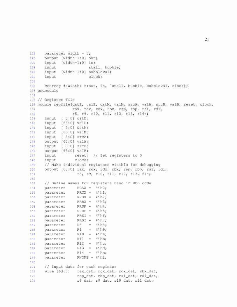
135 // Register file136 module regfile(dstE, valE, dstM, valM, srcA, valA, srcB, valB, reset, clock,137 rax, rcx, rdx, rbx, rsp, rbp, rsi, rdi,138 r8, r9, r10, r11, r12, r13, r14);139 input [ 3:0] dstE;140 input [63:0] valE;141 input [ 3:0] dstM;142 input [63:0] valM;143 input [ 3:0] srcA;144 output [63:0] valA;145 input [ 3:0] srcB;146 output [63:0] valB;147 input reset; // Set registers to 0148 input clock;149 // Make individual registers visible for debugging150 output [63:0] rax, rcx, rdx, rbx, rsp, rbp, rsi, rdi,151 r8, r9, r10, r11, r12, r13, r14;152
153 // Define names for registers used in HCL code154 parameter RRAX = 4’h0;155 parameter RRCX = 4’h1;156 parameter RRDX = 4’h2;157 parameter RRBX = 4’h3;158 parameter RRSP = 4’h4;159 parameter RRBP = 4’h5;160 parameter RRSI = 4’h6;161 parameter RRDI = 4’h7;162 parameter R8 = 4’h8;163 parameter R9 = 4’h9;164 parameter R10 = 4’ha;165 parameter R11 = 4’hb;166 parameter R12 = 4’hc;167 parameter R13 = 4’hd;168 parameter R14 = 4’he;169 parameter RNONE = 4’hf;170
171 // Input data for each register172 wire [63:0] rax_dat, rcx_dat, rdx_dat, rbx_dat,173 rsp_dat, rbp_dat, rsi_dat, rdi_dat,174 r8_dat, r9_dat, r10_dat, r11_dat,

22
175 r12_dat, r13_dat, r14_dat;176
177 // Input write controls for each register178 wire rax_wrt, rcx_wrt, rdx_wrt, rbx_wrt,179 rsp_wrt, rbp_wrt, rsi_wrt, rdi_wrt,180 r8_wrt, r9_wrt, r10_wrt, r11_wrt,181 r12_wrt, r13_wrt, r14_wrt;182
183
184 // Implement with clocked registers185 cenrreg #(64) rax_reg(rax, rax_dat, rax_wrt, reset, 64’b0, clock);186 cenrreg #(64) rcx_reg(rcx, rcx_dat, rcx_wrt, reset, 64’b0, clock);187 cenrreg #(64) rdx_reg(rdx, rdx_dat, rdx_wrt, reset, 64’b0, clock);188 cenrreg #(64) rbx_reg(rbx, rbx_dat, rbx_wrt, reset, 64’b0, clock);189 cenrreg #(64) rsp_reg(rsp, rsp_dat, rsp_wrt, reset, 64’b0, clock);190 cenrreg #(64) rbp_reg(rbp, rbp_dat, rbp_wrt, reset, 64’b0, clock);191 cenrreg #(64) rsi_reg(rsi, rsi_dat, rsi_wrt, reset, 64’b0, clock);192 cenrreg #(64) rdi_reg(rdi, rdi_dat, rdi_wrt, reset, 64’b0, clock);193 cenrreg #(64) r8_reg(r8, r8_dat, r8_wrt, reset, 64’b0, clock);194 cenrreg #(64) r9_reg(r9, r9_dat, r9_wrt, reset, 64’b0, clock);195 cenrreg #(64) r10_reg(r10, r10_dat, r10_wrt, reset, 64’b0, clock);196 cenrreg #(64) r11_reg(r11, r11_dat, r11_wrt, reset, 64’b0, clock);197 cenrreg #(64) r12_reg(r12, r12_dat, r12_wrt, reset, 64’b0, clock);198 cenrreg #(64) r13_reg(r13, r13_dat, r13_wrt, reset, 64’b0, clock);199 cenrreg #(64) r14_reg(r14, r14_dat, r14_wrt, reset, 64’b0, clock);200
201 // Reads occur like combinational logic202 assign valA =203 srcA == RRAX ? rax :204 srcA == RRCX ? rcx :205 srcA == RRDX ? rdx :206 srcA == RRBX ? rbx :207 srcA == RRSP ? rsp :208 srcA == RRBP ? rbp :209 srcA == RRSI ? rsi :210 srcA == RRDI ? rdi :211 srcA == R8 ? r8 :212 srcA == R9 ? r9 :213 srcA == R10 ? r10 :214 srcA == R11 ? r11 :215 srcA == R12 ? r12 :216 srcA == R13 ? r13 :217 srcA == R14 ? r14 :218 0;219
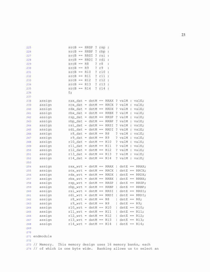
220 assign valB =221 srcB == RRAX ? rax :222 srcB == RRCX ? rcx :223 srcB == RRDX ? rdx :224 srcB == RRBX ? rbx :
23
225 srcB == RRSP ? rsp :226 srcB == RRBP ? rbp :227 srcB == RRSI ? rsi :228 srcB == RRDI ? rdi :229 srcB == R8 ? r8 :230 srcB == R9 ? r9 :231 srcB == R10 ? r10 :232 srcB == R11 ? r11 :233 srcB == R12 ? r12 :234 srcB == R13 ? r13 :235 srcB == R14 ? r14 :236 0;237
238 assign rax_dat = dstM == RRAX ? valM : valE;239 assign rcx_dat = dstM == RRCX ? valM : valE;240 assign rdx_dat = dstM == RRDX ? valM : valE;241 assign rbx_dat = dstM == RRBX ? valM : valE;242 assign rsp_dat = dstM == RRSP ? valM : valE;243 assign rbp_dat = dstM == RRBP ? valM : valE;244 assign rsi_dat = dstM == RRSI ? valM : valE;245 assign rdi_dat = dstM == RRDI ? valM : valE;246 assign r8_dat = dstM == R8 ? valM : valE;247 assign r9_dat = dstM == R9 ? valM : valE;248 assign r10_dat = dstM == R10 ? valM : valE;249 assign r11_dat = dstM == R11 ? valM : valE;250 assign r12_dat = dstM == R12 ? valM : valE;251 assign r13_dat = dstM == R13 ? valM : valE;252 assign r14_dat = dstM == R14 ? valM : valE;253
254 assign rax_wrt = dstM == RRAX | dstE == RRAX;255 assign rcx_wrt = dstM == RRCX | dstE == RRCX;256 assign rdx_wrt = dstM == RRDX | dstE == RRDX;257 assign rbx_wrt = dstM == RRBX | dstE == RRBX;258 assign rsp_wrt = dstM == RRSP | dstE == RRSP;259 assign rbp_wrt = dstM == RRBP | dstE == RRBP;260 assign rsi_wrt = dstM == RRSI | dstE == RRSI;261 assign rdi_wrt = dstM == RRDI | dstE == RRDI;262 assign r8_wrt = dstM == R8 | dstE == R8;263 assign r9_wrt = dstM == R9 | dstE == R9;264 assign r10_wrt = dstM == R10 | dstE == R10;265 assign r11_wrt = dstM == R11 | dstE == R11;266 assign r12_wrt = dstM == R12 | dstE == R12;267 assign r13_wrt = dstM == R13 | dstE == R13;268 assign r14_wrt = dstM == R14 | dstE == R14;269
270
271 endmodule272
273 // Memory. This memory design uses 16 memory banks, each274 // of which is one byte wide. Banking allows us to select an
24
275 // arbitrary set of 10 contiguous bytes for instruction reading276 // and an arbitrary set of 8 contiguous bytes277 // for data reading & writing.278 // It uses an external RAM module from either the file279 // combram.v (using combinational reads)280 // or synchram.v (using clocked reads)281 // The SEQ & SEQ+ processors only work with combram.v.282 // PIPE works with either.283
284 module bmemory(maddr, wenable, wdata, renable, rdata, m_ok,285 iaddr, instr, i_ok, clock);286 parameter memsize = 8192; // Number of bytes in memory287 input [63:0] maddr; // Read/Write address288 input wenable; // Write enable289 input [63:0] wdata; // Write data290 input renable; // Read enable291 output [63:0] rdata; // Read data292 output m_ok; // Read & write addresses within range293 input [63:0] iaddr; // Instruction address294 output [79:0] instr; // 10 bytes of instruction295 output i_ok; // Instruction address within range296 input clock;297
298 // Instruction bytes299 wire [ 7:0] ib0, ib1, ib2, ib3, ib4, ib5, ib6, ib7, ib8, ib9;300 // Data bytes301 wire [ 7:0] db0, db1, db2, db3, db4, db5, db6, db7;302
303 wire [ 3:0] ibid = iaddr[3:0]; // Instruction Bank ID304 wire [59:0] iindex = iaddr[63:4]; // Address within bank305 wire [59:0] iip1 = iindex+1; // Next address within bank306
307 wire [ 3:0] mbid = maddr[3:0]; // Data Bank ID308 wire [59:0] mindex = maddr[63:4]; // Address within bank309 wire [59:0] mip1 = mindex+1; // Next address within bank310
311 // Instruction addresses for each bank312 wire [59:0] addrI0, addrI1, addrI2, addrI3, addrI4, addrI5, addrI6, addrI7,313 addrI8, addrI9, addrI10, addrI11, addrI12, addrI13, addrI14,314 addrI15;315 // Instruction data for each bank316 wire [ 7:0] outI0, outI1, outI2, outI3, outI4, outI5, outI6, outI7,317 outI8, outI9, outI10, outI11, outI12, outI13, outI14, outI15;318
319 // Data addresses for each bank320 wire [59:0] addrD0, addrD1, addrD2, addrD3, addrD4, addrD5, addrD6, addrD7,321 addrD8, addrD9, addrD10, addrD11, addrD12, addrD13, addrD14,322 addrD15;323
324 // Data output for each bank

25
325 wire [ 7:0] outD0, outD1, outD2, outD3, outD4, outD5, outD6, outD7,326 outD8, outD9, outD10, outD11, outD12, outD13, outD14, outD15;327
328 // Data input for each bank329 wire [ 7:0] inD0, inD1, inD2, inD3, inD4, inD5, inD6, inD7,330 inD8, inD9, inD10, inD11, inD12, inD13, inD14, inD15;331
332 // Data write enable signals for each bank333 wire dwEn0, dwEn1, dwEn2, dwEn3, dwEn4, dwEn5, dwEn6, dwEn7,334 dwEn8, dwEn9, dwEn10, dwEn11, dwEn12, dwEn13, dwEn14, dwEn15;335
336 // The bank memories337 ram #(8, memsize/16, 60) bank0(clock,338 addrI0, 1’b0, 8’b0, 1’b1, outI0, // Instruction339 addrD0, dwEn0, inD0, renable, outD0); // Data340
341 ram #(8, memsize/16, 60) bank1(clock,342 addrI1, 1’b0, 8’b0, 1’b1, outI1, // Instruction343 addrD1, dwEn1, inD1, renable, outD1); // Data344
345 ram #(8, memsize/16, 60) bank2(clock,346 addrI2, 1’b0, 8’b0, 1’b1, outI2, // Instruction347 addrD2, dwEn2, inD2, renable, outD2); // Data348
349 ram #(8, memsize/16, 60) bank3(clock,350 addrI3, 1’b0, 8’b0, 1’b1, outI3, // Instruction351 addrD3, dwEn3, inD3, renable, outD3); // Data352
353 ram #(8, memsize/16, 60) bank4(clock,354 addrI4, 1’b0, 8’b0, 1’b1, outI4, // Instruction355 addrD4, dwEn4, inD4, renable, outD4); // Data356
357 ram #(8, memsize/16, 60) bank5(clock,358 addrI5, 1’b0, 8’b0, 1’b1, outI5, // Instruction359 addrD5, dwEn5, inD5, renable, outD5); // Data360
361 ram #(8, memsize/16, 60) bank6(clock,362 addrI6, 1’b0, 8’b0, 1’b1, outI6, // Instruction363 addrD6, dwEn6, inD6, renable, outD6); // Data364
365 ram #(8, memsize/16, 60) bank7(clock,366 addrI7, 1’b0, 8’b0, 1’b1, outI7, // Instruction367 addrD7, dwEn7, inD7, renable, outD7); // Data368
369 ram #(8, memsize/16, 60) bank8(clock,370 addrI8, 1’b0, 8’b0, 1’b1, outI8, // Instruction371 addrD8, dwEn8, inD8, renable, outD8); // Data372
373 ram #(8, memsize/16, 60) bank9(clock,374 addrI9, 1’b0, 8’b0, 1’b1, outI9, // Instruction

26
375 addrD9, dwEn9, inD9, renable, outD9); // Data376
377 ram #(8, memsize/16, 60) bank10(clock,378 addrI10, 1’b0, 8’b0, 1’b1, outI10, // Instruction379 addrD10, dwEn10, inD10, renable, outD10); // Data380
381 ram #(8, memsize/16, 60) bank11(clock,382 addrI11, 1’b0, 8’b0, 1’b1, outI11, // Instruction383 addrD11, dwEn11, inD11, renable, outD11); // Data384
385 ram #(8, memsize/16, 60) bank12(clock,386 addrI12, 1’b0, 8’b0, 1’b1, outI12, // Instruction387 addrD12, dwEn12, inD12, renable, outD12); // Data388
389 ram #(8, memsize/16, 60) bank13(clock,390 addrI13, 1’b0, 8’b0, 1’b1, outI13, // Instruction391 addrD13, dwEn13, inD13, renable, outD13); // Data392
393 ram #(8, memsize/16, 60) bank14(clock,394 addrI14, 1’b0, 8’b0, 1’b1, outI14, // Instruction395 addrD14, dwEn14, inD14, renable, outD14); // Data396
397 ram #(8, memsize/16, 60) bank15(clock,398 addrI15, 1’b0, 8’b0, 1’b1, outI15, // Instruction399 addrD15, dwEn15, inD15, renable, outD15); // Data400
401
402 // Determine the instruction addresses for the banks403 assign addrI0 = ibid >= 7 ? iip1 : iindex;404 assign addrI1 = ibid >= 8 ? iip1 : iindex;405 assign addrI2 = ibid >= 9 ? iip1 : iindex;406 assign addrI3 = ibid >= 10 ? iip1 : iindex;407 assign addrI4 = ibid >= 11 ? iip1 : iindex;408 assign addrI5 = ibid >= 12 ? iip1 : iindex;409 assign addrI6 = ibid >= 13 ? iip1 : iindex;410 assign addrI7 = ibid >= 14 ? iip1 : iindex;411 assign addrI8 = ibid >= 15 ? iip1 : iindex;412 assign addrI9 = iindex;413 assign addrI10 = iindex;414 assign addrI11 = iindex;415 assign addrI12 = iindex;416 assign addrI13 = iindex;417 assign addrI14 = iindex;418 assign addrI15 = iindex;419
420
421 // Get the bytes of the instruction422 assign i_ok =423 (iaddr + 9) < memsize;424
27
425 assign ib0 = !i_ok ? 0 :426 ibid == 0 ? outI0 :427 ibid == 1 ? outI1 :428 ibid == 2 ? outI2 :429 ibid == 3 ? outI3 :430 ibid == 4 ? outI4 :431 ibid == 5 ? outI5 :432 ibid == 6 ? outI6 :433 ibid == 7 ? outI7 :434 ibid == 8 ? outI8 :435 ibid == 9 ? outI9 :436 ibid == 10 ? outI10 :437 ibid == 11 ? outI11 :438 ibid == 12 ? outI12 :439 ibid == 13 ? outI13 :440 ibid == 14 ? outI14 :441 outI15;442 assign ib1 = !i_ok ? 0 :443 ibid == 0 ? outI1 :444 ibid == 1 ? outI2 :445 ibid == 2 ? outI3 :446 ibid == 3 ? outI4 :447 ibid == 4 ? outI5 :448 ibid == 5 ? outI6 :449 ibid == 6 ? outI7 :450 ibid == 7 ? outI8 :451 ibid == 8 ? outI9 :452 ibid == 9 ? outI10 :453 ibid == 10 ? outI11 :454 ibid == 11 ? outI12 :455 ibid == 12 ? outI13 :456 ibid == 13 ? outI14 :457 ibid == 14 ? outI15 :458 outI0;459 assign ib2 = !i_ok ? 0 :460 ibid == 0 ? outI2 :461 ibid == 1 ? outI3 :462 ibid == 2 ? outI4 :463 ibid == 3 ? outI5 :464 ibid == 4 ? outI6 :465 ibid == 5 ? outI7 :466 ibid == 6 ? outI8 :467 ibid == 7 ? outI9 :468 ibid == 8 ? outI10 :469 ibid == 9 ? outI11 :470 ibid == 10 ? outI12 :471 ibid == 11 ? outI13 :472 ibid == 12 ? outI14 :473 ibid == 13 ? outI15 :474 ibid == 14 ? outI0 :

28
475 outI1;476 assign ib3 = !i_ok ? 0 :477 ibid == 0 ? outI3 :478 ibid == 1 ? outI4 :479 ibid == 2 ? outI5 :480 ibid == 3 ? outI6 :481 ibid == 4 ? outI7 :482 ibid == 5 ? outI8 :483 ibid == 6 ? outI9 :484 ibid == 7 ? outI10 :485 ibid == 8 ? outI11 :486 ibid == 9 ? outI12 :487 ibid == 10 ? outI13 :488 ibid == 11 ? outI14 :489 ibid == 12 ? outI15 :490 ibid == 13 ? outI0 :491 ibid == 14 ? outI1 :492 outI2;493 assign ib4 = !i_ok ? 0 :494 ibid == 0 ? outI4 :495 ibid == 1 ? outI5 :496 ibid == 2 ? outI6 :497 ibid == 3 ? outI7 :498 ibid == 4 ? outI8 :499 ibid == 5 ? outI9 :500 ibid == 6 ? outI10 :501 ibid == 7 ? outI11 :502 ibid == 8 ? outI12 :503 ibid == 9 ? outI13 :504 ibid == 10 ? outI14 :505 ibid == 11 ? outI15 :506 ibid == 12 ? outI0 :507 ibid == 13 ? outI1 :508 ibid == 14 ? outI2 :509 outI3;510 assign ib5 = !i_ok ? 0 :511 ibid == 0 ? outI5 :512 ibid == 1 ? outI6 :513 ibid == 2 ? outI7 :514 ibid == 3 ? outI8 :515 ibid == 4 ? outI9 :516 ibid == 5 ? outI10 :517 ibid == 6 ? outI11 :518 ibid == 7 ? outI12 :519 ibid == 8 ? outI13 :520 ibid == 9 ? outI14 :521 ibid == 10 ? outI15 :522 ibid == 11 ? outI0 :523 ibid == 12 ? outI1 :524 ibid == 13 ? outI2 :

29
525 ibid == 14 ? outI3 :526 outI4;527 assign ib6 = !i_ok ? 0 :528 ibid == 0 ? outI6 :529 ibid == 1 ? outI7 :530 ibid == 2 ? outI8 :531 ibid == 3 ? outI9 :532 ibid == 4 ? outI10 :533 ibid == 5 ? outI11 :534 ibid == 6 ? outI12 :535 ibid == 7 ? outI13 :536 ibid == 8 ? outI14 :537 ibid == 9 ? outI15 :538 ibid == 10 ? outI0 :539 ibid == 11 ? outI1 :540 ibid == 12 ? outI2 :541 ibid == 13 ? outI3 :542 ibid == 14 ? outI4 :543 outI5;544 assign ib7 = !i_ok ? 0 :545 ibid == 0 ? outI7 :546 ibid == 1 ? outI8 :547 ibid == 2 ? outI9 :548 ibid == 3 ? outI10 :549 ibid == 4 ? outI11 :550 ibid == 5 ? outI12 :551 ibid == 6 ? outI13 :552 ibid == 7 ? outI14 :553 ibid == 8 ? outI15 :554 ibid == 9 ? outI0 :555 ibid == 10 ? outI1 :556 ibid == 11 ? outI2 :557 ibid == 12 ? outI3 :558 ibid == 13 ? outI4 :559 ibid == 14 ? outI5 :560 outI6;561 assign ib8 = !i_ok ? 0 :562 ibid == 0 ? outI8 :563 ibid == 1 ? outI9 :564 ibid == 2 ? outI10 :565 ibid == 3 ? outI11 :566 ibid == 4 ? outI12 :567 ibid == 5 ? outI13 :568 ibid == 6 ? outI14 :569 ibid == 7 ? outI15 :570 ibid == 8 ? outI0 :571 ibid == 9 ? outI1 :572 ibid == 10 ? outI2 :573 ibid == 11 ? outI3 :574 ibid == 12 ? outI4 :

30
575 ibid == 13 ? outI5 :576 ibid == 14 ? outI6 :577 outI7;578 assign ib9 = !i_ok ? 0 :579 ibid == 0 ? outI9 :580 ibid == 1 ? outI10 :581 ibid == 2 ? outI11 :582 ibid == 3 ? outI12 :583 ibid == 4 ? outI13 :584 ibid == 5 ? outI14 :585 ibid == 6 ? outI15 :586 ibid == 7 ? outI0 :587 ibid == 8 ? outI1 :588 ibid == 9 ? outI2 :589 ibid == 10 ? outI3 :590 ibid == 11 ? outI4 :591 ibid == 12 ? outI5 :592 ibid == 13 ? outI6 :593 ibid == 14 ? outI7 :594 outI8;595
596 assign instr[ 7: 0] = ib0;597 assign instr[15: 8] = ib1;598 assign instr[23:16] = ib2;599 assign instr[31:24] = ib3;600 assign instr[39:32] = ib4;601 assign instr[47:40] = ib5;602 assign instr[55:48] = ib6;603 assign instr[63:56] = ib7;604 assign instr[71:64] = ib8;605 assign instr[79:72] = ib9;606
607 assign m_ok =608 (!renable & !wenable | (maddr + 7) < memsize);609
610 assign addrD0 = mbid >= 9 ? mip1 : mindex;611 assign addrD1 = mbid >= 10 ? mip1 : mindex;612 assign addrD2 = mbid >= 11 ? mip1 : mindex;613 assign addrD3 = mbid >= 12 ? mip1 : mindex;614 assign addrD4 = mbid >= 13 ? mip1 : mindex;615 assign addrD5 = mbid >= 14 ? mip1 : mindex;616 assign addrD6 = mbid >= 15 ? mip1 : mindex;617 assign addrD7 = mindex;618 assign addrD8 = mindex;619 assign addrD9 = mindex;620 assign addrD10 = mindex;621 assign addrD11 = mindex;622 assign addrD12 = mindex;623 assign addrD13 = mindex;624 assign addrD14 = mindex;

31
625 assign addrD15 = mindex;626
627 // Get the bytes of data;628 assign db0 = !m_ok ? 0 :629 mbid == 0 ? outD0 :630 mbid == 1 ? outD1 :631 mbid == 2 ? outD2 :632 mbid == 3 ? outD3 :633 mbid == 4 ? outD4 :634 mbid == 5 ? outD5 :635 mbid == 6 ? outD6 :636 mbid == 7 ? outD7 :637 mbid == 8 ? outD8 :638 mbid == 9 ? outD9 :639 mbid == 10 ? outD10 :640 mbid == 11 ? outD11 :641 mbid == 12 ? outD12 :642 mbid == 13 ? outD13 :643 mbid == 14 ? outD14 :644 outD15;645 assign db1 = !m_ok ? 0 :646 mbid == 0 ? outD1 :647 mbid == 1 ? outD2 :648 mbid == 2 ? outD3 :649 mbid == 3 ? outD4 :650 mbid == 4 ? outD5 :651 mbid == 5 ? outD6 :652 mbid == 6 ? outD7 :653 mbid == 7 ? outD8 :654 mbid == 8 ? outD9 :655 mbid == 9 ? outD10 :656 mbid == 10 ? outD11 :657 mbid == 11 ? outD12 :658 mbid == 12 ? outD13 :659 mbid == 13 ? outD14 :660 mbid == 14 ? outD15 :661 outD0;662 assign db2 = !m_ok ? 0 :663 mbid == 0 ? outD2 :664 mbid == 1 ? outD3 :665 mbid == 2 ? outD4 :666 mbid == 3 ? outD5 :667 mbid == 4 ? outD6 :668 mbid == 5 ? outD7 :669 mbid == 6 ? outD8 :670 mbid == 7 ? outD9 :671 mbid == 8 ? outD10 :672 mbid == 9 ? outD11 :673 mbid == 10 ? outD12 :674 mbid == 11 ? outD13 :

32
675 mbid == 12 ? outD14 :676 mbid == 13 ? outD15 :677 mbid == 14 ? outD0 :678 outD1;679 assign db3 = !m_ok ? 0 :680 mbid == 0 ? outD3 :681 mbid == 1 ? outD4 :682 mbid == 2 ? outD5 :683 mbid == 3 ? outD6 :684 mbid == 4 ? outD7 :685 mbid == 5 ? outD8 :686 mbid == 6 ? outD9 :687 mbid == 7 ? outD10 :688 mbid == 8 ? outD11 :689 mbid == 9 ? outD12 :690 mbid == 10 ? outD13 :691 mbid == 11 ? outD14 :692 mbid == 12 ? outD15 :693 mbid == 13 ? outD0 :694 mbid == 14 ? outD1 :695 outD2;696 assign db4 = !m_ok ? 0 :697 mbid == 0 ? outD4 :698 mbid == 1 ? outD5 :699 mbid == 2 ? outD6 :700 mbid == 3 ? outD7 :701 mbid == 4 ? outD8 :702 mbid == 5 ? outD9 :703 mbid == 6 ? outD10 :704 mbid == 7 ? outD11 :705 mbid == 8 ? outD12 :706 mbid == 9 ? outD13 :707 mbid == 10 ? outD14 :708 mbid == 11 ? outD15 :709 mbid == 12 ? outD0 :710 mbid == 13 ? outD1 :711 mbid == 14 ? outD2 :712 outD3;713 assign db5 = !m_ok ? 0 :714 mbid == 0 ? outD5 :715 mbid == 1 ? outD6 :716 mbid == 2 ? outD7 :717 mbid == 3 ? outD8 :718 mbid == 4 ? outD9 :719 mbid == 5 ? outD10 :720 mbid == 6 ? outD11 :721 mbid == 7 ? outD12 :722 mbid == 8 ? outD13 :723 mbid == 9 ? outD14 :724 mbid == 10 ? outD15 :
33
725 mbid == 11 ? outD0 :726 mbid == 12 ? outD1 :727 mbid == 13 ? outD2 :728 mbid == 14 ? outD3 :729 outD4;730 assign db6 = !m_ok ? 0 :731 mbid == 0 ? outD6 :732 mbid == 1 ? outD7 :733 mbid == 2 ? outD8 :734 mbid == 3 ? outD9 :735 mbid == 4 ? outD10 :736 mbid == 5 ? outD11 :737 mbid == 6 ? outD12 :738 mbid == 7 ? outD13 :739 mbid == 8 ? outD14 :740 mbid == 9 ? outD15 :741 mbid == 10 ? outD0 :742 mbid == 11 ? outD1 :743 mbid == 12 ? outD2 :744 mbid == 13 ? outD3 :745 mbid == 14 ? outD4 :746 outD5;747 assign db7 = !m_ok ? 0 :748 mbid == 0 ? outD7 :749 mbid == 1 ? outD8 :750 mbid == 2 ? outD9 :751 mbid == 3 ? outD10 :752 mbid == 4 ? outD11 :753 mbid == 5 ? outD12 :754 mbid == 6 ? outD13 :755 mbid == 7 ? outD14 :756 mbid == 8 ? outD15 :757 mbid == 9 ? outD0 :758 mbid == 10 ? outD1 :759 mbid == 11 ? outD2 :760 mbid == 12 ? outD3 :761 mbid == 13 ? outD4 :762 mbid == 14 ? outD5 :763 outD6;764
765 assign rdata[ 7: 0] = db0;766 assign rdata[15: 8] = db1;767 assign rdata[23:16] = db2;768 assign rdata[31:24] = db3;769 assign rdata[39:32] = db4;770 assign rdata[47:40] = db5;771 assign rdata[55:48] = db6;772 assign rdata[63:56] = db7;773
774 wire [7:0] wd0 = wdata[ 7: 0];

34
775 wire [7:0] wd1 = wdata[15: 8];776 wire [7:0] wd2 = wdata[23:16];777 wire [7:0] wd3 = wdata[31:24];778 wire [7:0] wd4 = wdata[39:32];779 wire [7:0] wd5 = wdata[47:40];780 wire [7:0] wd6 = wdata[55:48];781 wire [7:0] wd7 = wdata[63:56];782
783 assign inD0 =784 mbid == 9 ? wd7 :785 mbid == 10 ? wd6 :786 mbid == 11 ? wd5 :787 mbid == 12 ? wd4 :788 mbid == 13 ? wd3 :789 mbid == 14 ? wd2 :790 mbid == 15 ? wd1 :791 mbid == 0 ? wd0 :792 0;793
794 assign inD1 =795 mbid == 10 ? wd7 :796 mbid == 11 ? wd6 :797 mbid == 12 ? wd5 :798 mbid == 13 ? wd4 :799 mbid == 14 ? wd3 :800 mbid == 15 ? wd2 :801 mbid == 0 ? wd1 :802 mbid == 1 ? wd0 :803 0;804
805 assign inD2 =806 mbid == 11 ? wd7 :807 mbid == 12 ? wd6 :808 mbid == 13 ? wd5 :809 mbid == 14 ? wd4 :810 mbid == 15 ? wd3 :811 mbid == 0 ? wd2 :812 mbid == 1 ? wd1 :813 mbid == 2 ? wd0 :814 0;815
816 assign inD3 =817 mbid == 12 ? wd7 :818 mbid == 13 ? wd6 :819 mbid == 14 ? wd5 :820 mbid == 15 ? wd4 :821 mbid == 0 ? wd3 :822 mbid == 1 ? wd2 :823 mbid == 2 ? wd1 :824 mbid == 3 ? wd0 :

35
825 0;826
827 assign inD4 =828 mbid == 13 ? wd7 :829 mbid == 14 ? wd6 :830 mbid == 15 ? wd5 :831 mbid == 0 ? wd4 :832 mbid == 1 ? wd3 :833 mbid == 2 ? wd2 :834 mbid == 3 ? wd1 :835 mbid == 4 ? wd0 :836 0;837
838 assign inD5 =839 mbid == 14 ? wd7 :840 mbid == 15 ? wd6 :841 mbid == 0 ? wd5 :842 mbid == 1 ? wd4 :843 mbid == 2 ? wd3 :844 mbid == 3 ? wd2 :845 mbid == 4 ? wd1 :846 mbid == 5 ? wd0 :847 0;848
849 assign inD6 =850 mbid == 15 ? wd7 :851 mbid == 0 ? wd6 :852 mbid == 1 ? wd5 :853 mbid == 2 ? wd4 :854 mbid == 3 ? wd3 :855 mbid == 4 ? wd2 :856 mbid == 5 ? wd1 :857 mbid == 6 ? wd0 :858 0;859
860 assign inD7 =861 mbid == 0 ? wd7 :862 mbid == 1 ? wd6 :863 mbid == 2 ? wd5 :864 mbid == 3 ? wd4 :865 mbid == 4 ? wd3 :866 mbid == 5 ? wd2 :867 mbid == 6 ? wd1 :868 mbid == 7 ? wd0 :869 0;870
871 assign inD8 =872 mbid == 1 ? wd7 :873 mbid == 2 ? wd6 :874 mbid == 3 ? wd5 :

36
875 mbid == 4 ? wd4 :876 mbid == 5 ? wd3 :877 mbid == 6 ? wd2 :878 mbid == 7 ? wd1 :879 mbid == 8 ? wd0 :880 0;881
882 assign inD9 =883 mbid == 2 ? wd7 :884 mbid == 3 ? wd6 :885 mbid == 4 ? wd5 :886 mbid == 5 ? wd4 :887 mbid == 6 ? wd3 :888 mbid == 7 ? wd2 :889 mbid == 8 ? wd1 :890 mbid == 9 ? wd0 :891 0;892
893 assign inD10 =894 mbid == 3 ? wd7 :895 mbid == 4 ? wd6 :896 mbid == 5 ? wd5 :897 mbid == 6 ? wd4 :898 mbid == 7 ? wd3 :899 mbid == 8 ? wd2 :900 mbid == 9 ? wd1 :901 mbid == 10 ? wd0 :902 0;903
904 assign inD11 =905 mbid == 4 ? wd7 :906 mbid == 5 ? wd6 :907 mbid == 6 ? wd5 :908 mbid == 7 ? wd4 :909 mbid == 8 ? wd3 :910 mbid == 9 ? wd2 :911 mbid == 10 ? wd1 :912 mbid == 11 ? wd0 :913 0;914
915 assign inD12 =916 mbid == 5 ? wd7 :917 mbid == 6 ? wd6 :918 mbid == 7 ? wd5 :919 mbid == 8 ? wd4 :920 mbid == 9 ? wd3 :921 mbid == 10 ? wd2 :922 mbid == 11 ? wd1 :923 mbid == 12 ? wd0 :924 0;
37
925
926 assign inD13 =927 mbid == 6 ? wd7 :928 mbid == 7 ? wd6 :929 mbid == 8 ? wd5 :930 mbid == 9 ? wd4 :931 mbid == 10 ? wd3 :932 mbid == 11 ? wd2 :933 mbid == 12 ? wd1 :934 mbid == 13 ? wd0 :935 0;936
937 assign inD14 =938 mbid == 7 ? wd7 :939 mbid == 8 ? wd6 :940 mbid == 9 ? wd5 :941 mbid == 10 ? wd4 :942 mbid == 11 ? wd3 :943 mbid == 12 ? wd2 :944 mbid == 13 ? wd1 :945 mbid == 14 ? wd0 :946 0;947
948 assign inD15 =949 mbid == 8 ? wd7 :950 mbid == 9 ? wd6 :951 mbid == 10 ? wd5 :952 mbid == 11 ? wd4 :953 mbid == 12 ? wd3 :954 mbid == 13 ? wd2 :955 mbid == 14 ? wd1 :956 mbid == 15 ? wd0 :957 0;958
959 // Which banks get written960 assign dwEn0 = wenable & (mbid <= 0 | mbid >= 9);961 assign dwEn1 = wenable & (mbid <= 1 | mbid >= 10);962 assign dwEn2 = wenable & (mbid <= 2 | mbid >= 11);963 assign dwEn3 = wenable & (mbid <= 3 | mbid >= 12);964 assign dwEn4 = wenable & (mbid <= 4 | mbid >= 13);965 assign dwEn5 = wenable & (mbid <= 5 | mbid >= 14);966 assign dwEn6 = wenable & (mbid <= 6 | mbid >= 15);967 assign dwEn7 = wenable & (mbid <= 7);968 assign dwEn8 = wenable & (mbid >= 1 & mbid <= 8);969 assign dwEn9 = wenable & (mbid >= 2 & mbid <= 9);970 assign dwEn10 = wenable & (mbid >= 3 & mbid <= 10);971 assign dwEn11 = wenable & (mbid >= 4 & mbid <= 11);972 assign dwEn12 = wenable & (mbid >= 5 & mbid <= 12);973 assign dwEn13 = wenable & (mbid >= 6 & mbid <= 13);974 assign dwEn14 = wenable & (mbid >= 7 & mbid <= 14);
38
975 assign dwEn15 = wenable & (mbid >= 8);976
977 endmodule978
979
980 // Combinational blocks981
982 // Fetch stage983
984 // Split instruction byte into icode and ifun fields985 module split(ibyte, icode, ifun);986 input [7:0] ibyte;987 output [3:0] icode;988 output [3:0] ifun;989
990 assign icode = ibyte[7:4];991 assign ifun = ibyte[3:0];992 endmodule993
994 // Extract immediate word from 9 bytes of instruction995 module align(ibytes, need_regids, rA, rB, valC);996 input [71:0] ibytes;997 input need_regids;998 output [ 3:0] rA;999 output [ 3:0] rB;1000 output [63:0] valC;1001 assign rA = ibytes[7:4];1002 assign rB = ibytes[3:0];1003 assign valC = need_regids ? ibytes[71:8] : ibytes[63:0];1004 endmodule1005
1006 // PC incrementer1007 module pc_increment(pc, need_regids, need_valC, valP);1008 input [63:0] pc;1009 input need_regids;1010 input need_valC;1011 output [63:0] valP;1012 assign valP = pc + 1 + 8*need_valC + need_regids;1013 endmodule1014
1015 // Execute Stage1016
1017 // ALU1018 module alu(aluA, aluB, alufun, valE, new_cc);1019 input [63:0] aluA, aluB; // Data inputs1020 input [ 3:0] alufun; // ALU function1021 output [63:0] valE; // Data Output1022 output [ 2:0] new_cc; // New values for ZF, SF, OF1023
1024 parameter ALUADD = 4’h0;
39
1025 parameter ALUSUB = 4’h1;1026 parameter ALUAND = 4’h2;1027 parameter ALUXOR = 4’h3;1028
1029 assign valE =1030 alufun == ALUSUB ? aluB - aluA :1031 alufun == ALUAND ? aluB & aluA :1032 alufun == ALUXOR ? aluB ˆ aluA :1033 aluB + aluA;1034 assign new_cc[2] = (valE == 0); // ZF1035 assign new_cc[1] = valE[63]; // SF1036 assign new_cc[0] = // OF1037 alufun == ALUADD ?1038 (aluA[63] == aluB[63]) & (aluA[63] != valE[63]) :1039 alufun == ALUSUB ?1040 (˜aluA[63] == aluB[63]) & (aluB[63] != valE[63]) :1041 0;1042 endmodule1043
1044
1045 // Condition code register1046 module cc(cc, new_cc, set_cc, reset, clock);1047 output[2:0] cc;1048 input [2:0] new_cc;1049 input set_cc;1050 input reset;1051 input clock;1052
1053 cenrreg #(3) c(cc, new_cc, set_cc, reset, 3’b100, clock);1054 endmodule1055
1056 // branch condition logic1057 module cond(ifun, cc, Cnd);1058 input [3:0] ifun;1059 input [2:0] cc;1060 output Cnd;1061
1062 wire zf = cc[2];1063 wire sf = cc[1];1064 wire of = cc[0];1065
1066 // Jump & move conditions.1067 parameter C_YES = 4’h0;1068 parameter C_LE = 4’h1;1069 parameter C_L = 4’h2;1070 parameter C_E = 4’h3;1071 parameter C_NE = 4’h4;1072 parameter C_GE = 4’h5;1073 parameter C_G = 4’h6;1074

40
1075 assign Cnd =1076 (ifun == C_YES) | //1077 (ifun == C_LE & ((sfˆof)|zf)) | // <=1078 (ifun == C_L & (sfˆof)) | // <1079 (ifun == C_E & zf) | // ==1080 (ifun == C_NE & ˜zf) | // !=1081 (ifun == C_GE & (˜sfˆof)) | // >=1082 (ifun == C_G & (˜sfˆof)&˜zf); // >1083
1084 endmodule1085
1086 // --------------------------------------------------------------------1087 // Processor implementation1088 // --------------------------------------------------------------------1089
1090
1091 // The processor can run in 5 different modes:1092 // RUN: Normal operation1093 // RESET: Sets PC to 0, clears all pipe registers;1094 // Initializes condition codes1095 // DOWNLOAD: Download bytes from controller into memory1096 // UPLOAD: Upload bytes from memory to controller1097 // STATUS: Upload other status information to controller1098
1099 // Processor module1100 module processor(mode, udaddr, idata, odata, stat, clock);1101 input [ 2:0] mode; // Signal operating mode to processor1102 input [63:0] udaddr; // Upload/download address1103 input [63:0] idata; // Download data word1104 output [63:0] odata; // Upload data word1105 output [ 2:0] stat; // Status1106 input clock; // Clock input1107
1108 // Define modes1109 parameter RUN_MODE = 0; // Normal operation1110 parameter RESET_MODE = 1; // Resetting processor;1111 parameter DOWNLOAD_MODE = 2; // Transfering to memory1112 parameter UPLOAD_MODE = 3; // Reading from memory1113 // Uploading register & other status information1114 parameter STATUS_MODE = 4;1115
1116 // Constant values1117
1118 // Instruction codes1119 parameter IHALT = 4’h0;1120 parameter INOP = 4’h1;1121 parameter IRRMOVQ = 4’h2;1122 parameter IIRMOVQ = 4’h3;1123 parameter IRMMOVQ = 4’h4;1124 parameter IMRMOVQ = 4’h5;

41
1125 parameter IOPQ = 4’h6;1126 parameter IJXX = 4’h7;1127 parameter ICALL = 4’h8;1128 parameter IRET = 4’h9;1129 parameter IPUSHQ = 4’hA;1130 parameter IPOPQ = 4’hB;1131 parameter IIADDQ = 4’hC;1132 parameter ILEAVE = 4’hD;1133 parameter IPOP2 = 4’hE;1134
1135 // Function codes1136 parameter FNONE = 4’h0;1137
1138 // Jump conditions1139 parameter UNCOND = 4’h0;1140
1141 // Register IDs1142 parameter RRSP = 4’h4;1143 parameter RRBP = 4’h5;1144 parameter RNONE = 4’hF;1145
1146 // ALU operations1147 parameter ALUADD = 4’h0;1148
1149 // Status conditions1150 parameter SBUB = 3’h0;1151 parameter SAOK = 3’h1;1152 parameter SHLT = 3’h2;1153 parameter SADR = 3’h3;1154 parameter SINS = 3’h4;1155 parameter SPIP = 3’h5;1156
1157 // Fetch stage signals1158 wire [63:0] f_predPC, F_predPC, f_pc;1159 wire f_ok;1160 wire imem_error;1161 wire [ 2:0] f_stat;1162 wire [79:0] f_instr;1163 wire [ 3:0] imem_icode;1164 wire [ 3:0] imem_ifun;1165 wire [ 3:0] f_icode;1166 wire [ 3:0] f_ifun;1167 wire [ 3:0] f_rA;1168 wire [ 3:0] f_rB;1169 wire [63:0] f_valC;1170 wire [63:0] f_valP;1171 wire need_regids;1172 wire need_valC;1173 wire instr_valid;1174 wire F_stall, F_bubble;

42
1175
1176 // Decode stage signals1177 wire [ 2:0] D_stat;1178 wire [63:0] D_pc;1179 wire [ 3:0] D_icode;1180 wire [ 3:0] D_ifun;1181 wire [ 3:0] D_rA;1182 wire [ 3:0] D_rB;1183 wire [63:0] D_valC;1184 wire [63:0] D_valP;1185
1186 wire [63:0] d_valA;1187 wire [63:0] d_valB;1188 wire [63:0] d_rvalA;1189 wire [63:0] d_rvalB;1190 wire [ 3:0] d_dstE;1191 wire [ 3:0] d_dstM;1192 wire [ 3:0] d_srcA;1193 wire [ 3:0] d_srcB;1194 wire D_stall, D_bubble;1195
1196 // Execute stage signals1197 wire [ 2:0] E_stat;1198 wire [63:0] E_pc;1199 wire [ 3:0] E_icode;1200 wire [ 3:0] E_ifun;1201 wire [63:0] E_valC;1202 wire [63:0] E_valA;1203 wire [63:0] E_valB;1204 wire [ 3:0] E_dstE;1205 wire [ 3:0] E_dstM;1206 wire [ 3:0] E_srcA;1207 wire [ 3:0] E_srcB;1208
1209 wire [63:0] aluA;1210 wire [63:0] aluB;1211 wire set_cc;1212 wire [ 2:0] cc;1213 wire [ 2:0] new_cc;1214 wire [ 3:0] alufun;1215 wire e_Cnd;1216 wire [63:0] e_valE;1217 wire [63:0] e_valA;1218 wire [ 3:0] e_dstE;1219 wire E_stall, E_bubble;1220
1221 // Memory stage1222 wire [ 2:0] M_stat;1223 wire [63:0] M_pc;1224 wire [ 3:0] M_icode;

43
1225 wire [ 3:0] M_ifun;1226 wire M_Cnd;1227 wire [63:0] M_valE;1228 wire [63:0] M_valA;1229 wire [ 3:0] M_dstE;1230 wire [ 3:0] M_dstM;1231
1232 wire [ 2:0] m_stat;1233 wire [63:0] mem_addr;1234 wire [63:0] mem_data;1235 wire mem_read;1236 wire mem_write;1237 wire [63:0] m_valM;1238 wire M_stall, M_bubble;1239 wire m_ok;1240
1241 // Write-back stage1242 wire [ 2:0] W_stat;1243 wire [63:0] W_pc;1244 wire [ 3:0] W_icode;1245 wire [63:0] W_valE;1246 wire [63:0] W_valM;1247 wire [ 3:0] W_dstE;1248 wire [ 3:0] W_dstM;1249 wire [63:0] w_valE;1250 wire [63:0] w_valM;1251 wire [ 3:0] w_dstE;1252 wire [ 3:0] w_dstM;1253 wire W_stall, W_bubble;1254
1255 // Global status1256 wire [ 2:0] Stat;1257
1258 // Debugging logic1259 wire [63:0] rax, rcx, rdx, rbx, rsp, rbp, rsi, rdi,1260 r8, r9, r10, r11, r12, r13, r14;1261 wire zf = cc[2];1262 wire sf = cc[1];1263 wire of = cc[0];1264
1265 // Control signals1266 wire resetting = (mode == RESET_MODE);1267 wire uploading = (mode == UPLOAD_MODE);1268 wire downloading = (mode == DOWNLOAD_MODE);1269 wire running = (mode == RUN_MODE);1270 wire getting_info = (mode == STATUS_MODE);1271 // Logic to control resetting of pipeline registers1272 wire F_reset = F_bubble | resetting;1273 wire D_reset = D_bubble | resetting;1274 wire E_reset = E_bubble | resetting;

44
1275 wire M_reset = M_bubble | resetting;1276 wire W_reset = W_bubble | resetting;1277
1278 // Processor status1279 assign stat = Stat;1280 // Output data1281 assign odata =1282 // When getting status, get either register or special status value1283 getting_info ?1284 (udaddr == 0 ? rax :1285 udaddr == 8 ? rcx :1286 udaddr == 16 ? rdx :1287 udaddr == 24 ? rbx :1288 udaddr == 32 ? rsp :1289 udaddr == 40 ? rbp :1290 udaddr == 48 ? rsi :1291 udaddr == 56 ? rdi :1292 udaddr == 64 ? r8 :1293 udaddr == 72 ? r9 :1294 udaddr == 80 ? r10 :1295 udaddr == 88 ? r11 :1296 udaddr == 96 ? r12 :1297 udaddr == 104 ? r13 :1298 udaddr == 112 ? r14 :1299 udaddr == 120 ? cc :1300 udaddr == 128 ? W_pc : 0)1301 : m_valM;1302
1303 // Pipeline registers1304
1305 // All pipeline registers are implemented with module1306 // preg(out, in, stall, bubble, bubbleval, clock)1307 // F Register1308 preg #(64) F_predPC_reg(F_predPC, f_predPC, F_stall, F_reset, 64’b0, clock);1309 // D Register1310 preg #(3) D_stat_reg(D_stat, f_stat, D_stall, D_reset, SBUB, clock);1311 preg #(64) D_pc_reg(D_pc, f_pc, D_stall, D_reset, 64’b0, clock);1312 preg #(4) D_icode_reg(D_icode, f_icode, D_stall, D_reset, INOP, clock);1313 preg #(4) D_ifun_reg(D_ifun, f_ifun, D_stall, D_reset, FNONE, clock);1314 preg #(4) D_rA_reg(D_rA, f_rA, D_stall, D_reset, RNONE, clock);1315 preg #(4) D_rB_reg(D_rB, f_rB, D_stall, D_reset, RNONE, clock);1316 preg #(64) D_valC_reg(D_valC, f_valC, D_stall, D_reset, 64’b0, clock);1317 preg #(64) D_valP_reg(D_valP, f_valP, D_stall, D_reset, 64’b0, clock);1318 // E Register1319 preg #(3) E_stat_reg(E_stat, D_stat, E_stall, E_reset, SBUB, clock);1320 preg #(64) E_pc_reg(E_pc, D_pc, E_stall, E_reset, 64’b0, clock);1321 preg #(4) E_icode_reg(E_icode, D_icode, E_stall, E_reset, INOP, clock);1322 preg #(4) E_ifun_reg(E_ifun, D_ifun, E_stall, E_reset, FNONE, clock);1323 preg #(64) E_valC_reg(E_valC, D_valC, E_stall, E_reset, 64’b0, clock);1324 preg #(64) E_valA_reg(E_valA, d_valA, E_stall, E_reset, 64’b0, clock);

45
1325 preg #(64) E_valB_reg(E_valB, d_valB, E_stall, E_reset, 64’b0, clock);1326 preg #(4) E_dstE_reg(E_dstE, d_dstE, E_stall, E_reset, RNONE, clock);1327 preg #(4) E_dstM_reg(E_dstM, d_dstM, E_stall, E_reset, RNONE, clock);1328 preg #(4) E_srcA_reg(E_srcA, d_srcA, E_stall, E_reset, RNONE, clock);1329 preg #(4) E_srcB_reg(E_srcB, d_srcB, E_stall, E_reset, RNONE, clock);1330 // M Register1331 preg #(3) M_stat_reg(M_stat, E_stat, M_stall, M_reset, SBUB, clock);1332 preg #(64) M_pc_reg(M_pc, E_pc, M_stall, M_reset, 64’b0, clock);1333 preg #(4) M_icode_reg(M_icode, E_icode, M_stall, M_reset, INOP, clock);1334 preg #(4) M_ifun_reg(M_ifun, E_ifun, M_stall, M_reset, FNONE, clock);1335 preg #(1) M_Cnd_reg(M_Cnd, e_Cnd, M_stall, M_reset, 1’b0, clock);1336 preg #(64) M_valE_reg(M_valE, e_valE, M_stall, M_reset, 64’b0, clock);1337 preg #(64) M_valA_reg(M_valA, e_valA, M_stall, M_reset, 64’b0, clock);1338 preg #(4) M_dstE_reg(M_dstE, e_dstE, M_stall, M_reset, RNONE, clock);1339 preg #(4) M_dstM_reg(M_dstM, E_dstM, M_stall, M_reset, RNONE, clock);1340 // W Register1341 preg #(3) W_stat_reg(W_stat, m_stat, W_stall, W_reset, SBUB, clock);1342 preg #(64) W_pc_reg(W_pc, M_pc, W_stall, W_reset, 64’b0, clock);1343 preg #(4) W_icode_reg(W_icode, M_icode, W_stall, W_reset, INOP, clock);1344 preg #(64) W_valE_reg(W_valE, M_valE, W_stall, W_reset, 64’b0, clock);1345 preg #(64) W_valM_reg(W_valM, m_valM, W_stall, W_reset, 64’b0, clock);1346 preg #(4) W_dstE_reg(W_dstE, M_dstE, W_stall, W_reset, RNONE, clock);1347 preg #(4) W_dstM_reg(W_dstM, M_dstM, W_stall, W_reset, RNONE, clock);1348
1349 // Fetch stage logic1350 split split(f_instr[7:0], imem_icode, imem_ifun);1351 align align(f_instr[79:8], need_regids, f_rA, f_rB, f_valC);1352 pc_increment pci(f_pc, need_regids, need_valC, f_valP);1353
1354 // Decode stage1355 regfile regf(w_dstE, w_valE, w_dstM, w_valM,1356 d_srcA, d_rvalA, d_srcB, d_rvalB, resetting, clock,1357 rax, rcx, rdx, rbx, rsp, rbp, rsi, rdi,1358 r8, r9, r10, r11, r12, r13, r14);1359
1360
1361 // Execute stage1362 alu alu(aluA, aluB, alufun, e_valE, new_cc);1363 cc ccreg(cc, new_cc,1364 // Only update CC when everything is running normally1365 running & set_cc,1366 resetting, clock);1367 cond cond_check(E_ifun, cc, e_Cnd);1368
1369 // Memory stage1370 bmemory m(1371 // Only update memory when everything is running normally1372 // or when downloading1373 (downloading | uploading) ? udaddr : mem_addr, // Read/Write address1374 (running & mem_write) | downloading, // When to write to memory

46
1375 downloading ? idata : M_valA, // Write data1376 (running & mem_read) | uploading, // When to read memory1377 m_valM, // Read data1378 m_ok,1379 f_pc, f_instr, f_ok, clock); // Instruction memory access1380
1381 assign imem_error = ˜f_ok;1382 assign dmem_error = ˜m_ok;1383
1384 // Write-back stage logic1385
1386 // Control logic1387 // --------------------------------------------------------------------1388 // The following code is generated from the HCL description of the1389 // pipeline control using the hcl2v program1390 // --------------------------------------------------------------------1391 assign f_pc =1392 (((M_icode == IJXX) & ˜M_Cnd) ? M_valA : (W_icode == IRET) ? W_valM :1393 F_predPC);1394
1395 assign f_icode =1396 (imem_error ? INOP : imem_icode);1397
1398 assign f_ifun =1399 (imem_error ? FNONE : imem_ifun);1400
1401 assign instr_valid =1402 (f_icode == INOP | f_icode == IHALT | f_icode == IRRMOVQ | f_icode ==1403 IIRMOVQ | f_icode == IRMMOVQ | f_icode == IMRMOVQ | f_icode == IOPQ1404 | f_icode == IJXX | f_icode == ICALL | f_icode == IRET | f_icode ==1405 IPUSHQ | f_icode == IPOPQ);1406
1407 assign f_stat =1408 (imem_error ? SADR : ˜instr_valid ? SINS : (f_icode == IHALT) ? SHLT :1409 SAOK);1410
1411 assign need_regids =1412 (f_icode == IRRMOVQ | f_icode == IOPQ | f_icode == IPUSHQ | f_icode ==1413 IPOPQ | f_icode == IIRMOVQ | f_icode == IRMMOVQ | f_icode == IMRMOVQ)1414 ;1415
1416 assign need_valC =1417 (f_icode == IIRMOVQ | f_icode == IRMMOVQ | f_icode == IMRMOVQ | f_icode1418 == IJXX | f_icode == ICALL);1419
1420 assign f_predPC =1421 ((f_icode == IJXX | f_icode == ICALL) ? f_valC : f_valP);1422
1423 assign d_srcA =1424 ((D_icode == IRRMOVQ | D_icode == IRMMOVQ | D_icode == IOPQ | D_icode

47
1425 == IPUSHQ) ? D_rA : (D_icode == IPOPQ | D_icode == IRET) ? RRSP :1426 RNONE);1427
1428 assign d_srcB =1429 ((D_icode == IOPQ | D_icode == IRMMOVQ | D_icode == IMRMOVQ) ? D_rB : (1430 D_icode == IPUSHQ | D_icode == IPOPQ | D_icode == ICALL | D_icode1431 == IRET) ? RRSP : RNONE);1432
1433 assign d_dstE =1434 ((D_icode == IRRMOVQ | D_icode == IIRMOVQ | D_icode == IOPQ) ? D_rB : (1435 D_icode == IPUSHQ | D_icode == IPOPQ | D_icode == ICALL | D_icode1436 == IRET) ? RRSP : RNONE);1437
1438 assign d_dstM =1439 ((D_icode == IMRMOVQ | D_icode == IPOPQ) ? D_rA : RNONE);1440
1441 assign d_valA =1442 ((D_icode == ICALL | D_icode == IJXX) ? D_valP : (d_srcA == e_dstE) ?1443 e_valE : (d_srcA == M_dstM) ? m_valM : (d_srcA == M_dstE) ? M_valE :1444 (d_srcA == W_dstM) ? W_valM : (d_srcA == W_dstE) ? W_valE : d_rvalA);1445
1446 assign d_valB =1447 ((d_srcB == e_dstE) ? e_valE : (d_srcB == M_dstM) ? m_valM : (d_srcB1448 == M_dstE) ? M_valE : (d_srcB == W_dstM) ? W_valM : (d_srcB ==1449 W_dstE) ? W_valE : d_rvalB);1450
1451 assign aluA =1452 ((E_icode == IRRMOVQ | E_icode == IOPQ) ? E_valA : (E_icode == IIRMOVQ1453 | E_icode == IRMMOVQ | E_icode == IMRMOVQ) ? E_valC : (E_icode ==1454 ICALL | E_icode == IPUSHQ) ? -8 : (E_icode == IRET | E_icode == IPOPQ1455 ) ? 8 : 0);1456
1457 assign aluB =1458 ((E_icode == IRMMOVQ | E_icode == IMRMOVQ | E_icode == IOPQ | E_icode1459 == ICALL | E_icode == IPUSHQ | E_icode == IRET | E_icode == IPOPQ)1460 ? E_valB : (E_icode == IRRMOVQ | E_icode == IIRMOVQ) ? 0 : 0);1461
1462 assign alufun =1463 ((E_icode == IOPQ) ? E_ifun : ALUADD);1464
1465 assign set_cc =1466 (((E_icode == IOPQ) & ˜(m_stat == SADR | m_stat == SINS | m_stat ==1467 SHLT)) & ˜(W_stat == SADR | W_stat == SINS | W_stat == SHLT));1468
1469 assign e_valA =1470 E_valA;1471
1472 assign e_dstE =1473 (((E_icode == IRRMOVQ) & ˜e_Cnd) ? RNONE : E_dstE);1474

48
1475 assign mem_addr =1476 ((M_icode == IRMMOVQ | M_icode == IPUSHQ | M_icode == ICALL | M_icode1477 == IMRMOVQ) ? M_valE : (M_icode == IPOPQ | M_icode == IRET) ?1478 M_valA : 0);1479
1480 assign mem_read =1481 (M_icode == IMRMOVQ | M_icode == IPOPQ | M_icode == IRET);1482
1483 assign mem_write =1484 (M_icode == IRMMOVQ | M_icode == IPUSHQ | M_icode == ICALL);1485
1486 assign m_stat =1487 (dmem_error ? SADR : M_stat);1488
1489 assign w_dstE =1490 W_dstE;1491
1492 assign w_valE =1493 W_valE;1494
1495 assign w_dstM =1496 W_dstM;1497
1498 assign w_valM =1499 W_valM;1500
1501 assign Stat =1502 ((W_stat == SBUB) ? SAOK : W_stat);1503
1504 assign F_bubble =1505 0;1506
1507 assign F_stall =1508 (((E_icode == IMRMOVQ | E_icode == IPOPQ) & (E_dstM == d_srcA | E_dstM1509 == d_srcB)) | (IRET == D_icode | IRET == E_icode | IRET ==1510 M_icode));1511
1512 assign D_stall =1513 ((E_icode == IMRMOVQ | E_icode == IPOPQ) & (E_dstM == d_srcA | E_dstM1514 == d_srcB));1515
1516 assign D_bubble =1517 (((E_icode == IJXX) & ˜e_Cnd) | (˜((E_icode == IMRMOVQ | E_icode ==1518 IPOPQ) & (E_dstM == d_srcA | E_dstM == d_srcB)) & (IRET ==1519 D_icode | IRET == E_icode | IRET == M_icode)));1520
1521 assign E_stall =1522 0;1523
1524 assign E_bubble =
49
1525 (((E_icode == IJXX) & ˜e_Cnd) | ((E_icode == IMRMOVQ | E_icode == IPOPQ1526 ) & (E_dstM == d_srcA | E_dstM == d_srcB)));1527
1528 assign M_stall =1529 0;1530
1531 assign M_bubble =1532 ((m_stat == SADR | m_stat == SINS | m_stat == SHLT) | (W_stat == SADR1533 | W_stat == SINS | W_stat == SHLT));1534
1535 assign W_stall =1536 (W_stat == SADR | W_stat == SINS | W_stat == SHLT);1537
1538 assign W_bubble =1539 0;1540
1541 // --------------------------------------------------------------------1542 // End of code generated by hcl2v1543 // --------------------------------------------------------------------1544 endmodule1545
References
[1] D. Thomas and P. Moorby. The Verilog Hardware Description Language, Fifth Edition. Springer, 2008.
IndexCS:APP3e , 1
conditional expression (Verilog), 5continuous assignment (Verilog), 4
Design Compiler, 2
Goel, Prabhu, 1
memory bank, Y86-64 processor, 9module, Verilog, 4Moorby, Philip, 1multiplexor, 5
non-blocking assignment, Verilog, 7
reg, Verilog state-holding signal, 7
Synopsys, Inc., 2
wire, Verilog combinational signal, 2, 7, 14
50