PARDIS: A Programmable Memory Controller for the DDRx Interfacing
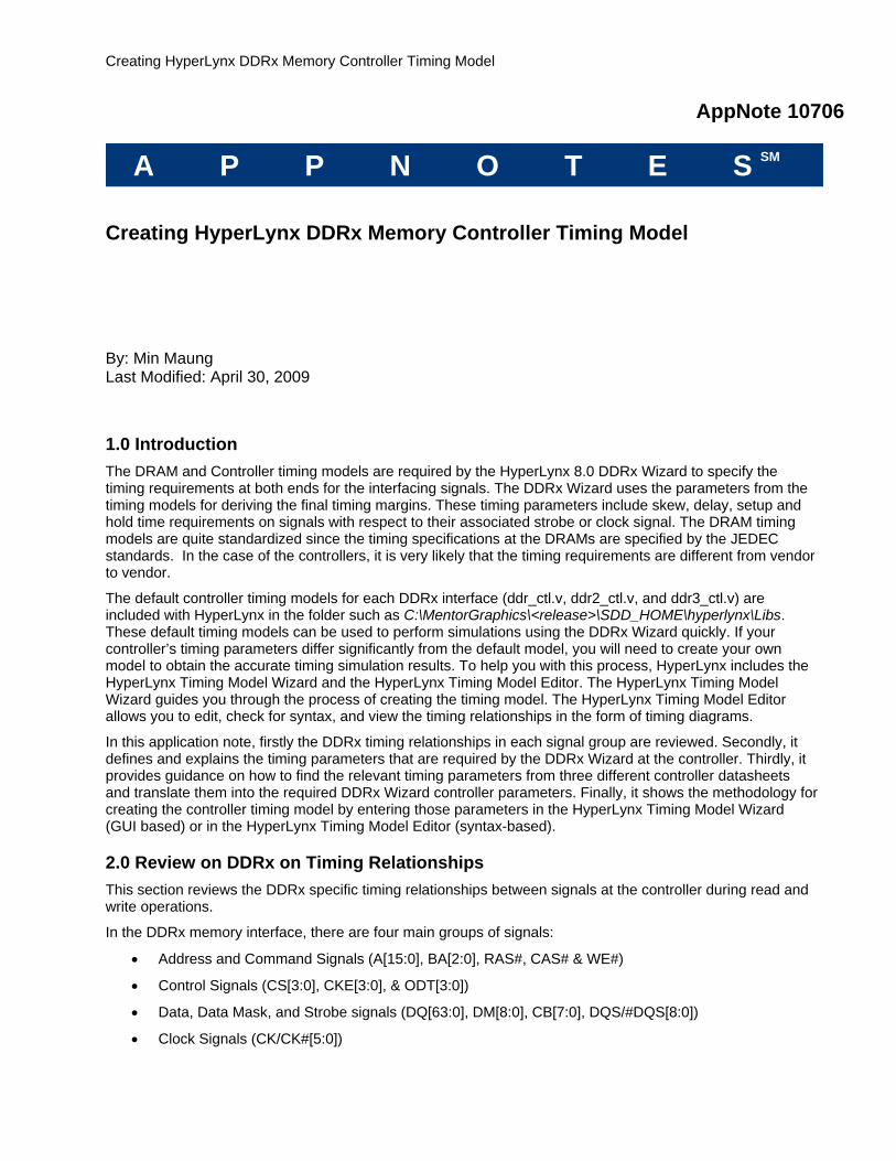
Creating HyperLynx DDRx Memory Controller Timing Model
AppNote 10706
A P P N O T E S SM
Creating HyperLynx DDRx Memory Controller Timing Model By: Min Maung Last Modified: April 30, 2009
1.0 Introduction The DRAM and Controller timing models are required by the HyperLynx 8.0 DDRx Wizard to specify the timing requirements at both ends for the interfacing signals. The DDRx Wizard uses the parameters from the timing models for deriving the final timing margins. These timing parameters include skew, delay, setup and hold time requirements on signals with respect to their associated strobe or clock signal. The DRAM timing models are quite standardized since the timing specifications at the DRAMs are specified by the JEDEC standards. In the case of the controllers, it is very likely that the timing requirements are different from vendor to vendor.
The default controller timing models for each DDRx interface (ddr_ctl.v, ddr2_ctl.v, and ddr3_ctl.v) are included with HyperLynx in the folder such as C:\MentorGraphics\<release>\SDD_HOME\hyperlynx\Libs. These default timing models can be used to perform simulations using the DDRx Wizard quickly. If your controller’s timing parameters differ significantly from the default model, you will need to create your own model to obtain the accurate timing simulation results. To help you with this process, HyperLynx includes the HyperLynx Timing Model Wizard and the HyperLynx Timing Model Editor. The HyperLynx Timing Model Wizard guides you through the process of creating the timing model. The HyperLynx Timing Model Editor allows you to edit, check for syntax, and view the timing relationships in the form of timing diagrams.
In this application note, firstly the DDRx timing relationships in each signal group are reviewed. Secondly, it defines and explains the timing parameters that are required by the DDRx Wizard at the controller. Thirdly, it provides guidance on how to find the relevant timing parameters from three different controller datasheets and translate them into the required DDRx Wizard controller parameters. Finally, it shows the methodology for creating the controller timing model by entering those parameters in the HyperLynx Timing Model Wizard (GUI based) or in the HyperLynx Timing Model Editor (syntax-based).
2.0 Review on DDRx on Timing Relationships This section reviews the DDRx specific timing relationships between signals at the controller during read and write operations.
In the DDRx memory interface, there are four main groups of signals:
• Address and Command Signals (A[15:0], BA[2:0], RAS#, CAS# & WE#)
• Control Signals (CS[3:0], CKE[3:0], & ODT[3:0])
• Data, Data Mask, and Strobe signals (DQ[63:0], DM[8:0], CB[7:0], DQS/#DQS[8:0])
• Clock Signals (CK/CK#[5:0])
First, the operating frequency of the clock signal must be determined. The DDRx interface is usually specified by notation DDRx–<speed-grade>, for example DDR-400, DDR2-533 or DDR3-800. The speed-grade unit is in MT/s (mega-transfer per second). In this application note, DDR3-800 will be used as an example throughout. In this case, the speed-grade is 800MT/s, and the operating frequency is half of the speed-grade; 400MHz. The bit period for address/command/control and data signals is needed information.
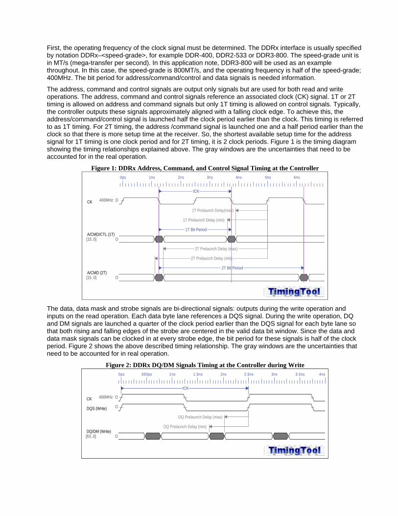
The address, command and control signals are output only signals but are used for both read and write operations. The address, command and control signals reference an associated clock (CK) signal. 1T or 2T timing is allowed on address and command signals but only 1T timing is allowed on control signals. Typically, the controller outputs these signals approximately aligned with a falling clock edge. To achieve this, the address/command/control signal is launched half the clock period earlier than the clock. This timing is referred to as 1T timing. For 2T timing, the address /command signal is launched one and a half period earlier than the clock so that there is more setup time at the receiver. So, the shortest available setup time for the address signal for 1T timing is one clock period and for 2T timing, it is 2 clock periods. Figure 1 is the timing diagram showing the timing relationships explained above. The gray windows are the uncertainties that need to be accounted for in the real operation.
Figure 1: DDRx Address, Command, and Control Signal Timing at the Controller 0ps 1ns 2ns 3ns 4ns 5ns 6ns
CK O400MHz
A/CMD/CTL (1T)O[15..0]
A/CMD (2T)O[15..0]
tCK
1T Bit Period
2T Bit Period
1T Prelaunch Delay(max)
1T Prelaunch Delay (min)
2T Prelaunch Delay (max)
2T Prelaunch Delay (min)
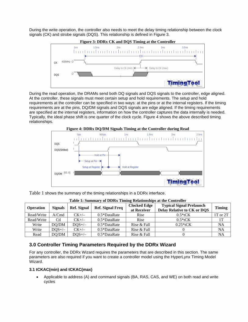
The data, data mask and strobe signals are bi-directional signals: outputs during the write operation and inputs on the read operation. Each data byte lane references a DQS signal. During the write operation, DQ and DM signals are launched a quarter of the clock period earlier than the DQS signal for each byte lane so that both rising and falling edges of the strobe are centered in the valid data bit window. Since the data and data mask signals can be clocked in at every strobe edge, the bit period for these signals is half of the clock period. Figure 2 shows the above described timing relationship. The gray windows are the uncertainties that need to be accounted for in real operation.
Figure 2: DDRx DQ/DM Signals Timing at the Controller during Write 0ps 500ps 1ns 1.5ns 2ns 2.5ns 3ns 3.5ns 4ns
CK O400MHz
DQS (Write) O
DQ/DM (Write)O[63..0]
tCK
DQ Prelaunch Delay (max)
DQ Prelaunch Delay (min)
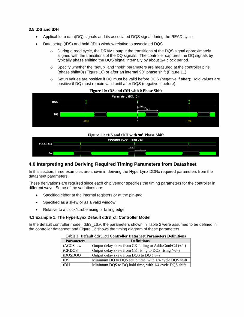
During the write operation, the controller also needs to meet the delay timing relationship between the clock signals (CK) and strobe signals (DQS). This relationship is defined in Figure 3.
Figure 3: DDRx CK and DQS Timing at the Controller 1ns 1.5ns 2ns 2.5ns 3ns 3.5ns
CK O400MHz
DQS O
tCK
Delay to CK (min) Delay to CK (max)
During the read operation, the DRAMs send both DQ signals and DQS signals to the controller, edge aligned. At the controller, these signals must meet certain setup and hold requirements. The setup and hold requirements at the controller can be specified in two ways: at the pins or at the internal registers. If the timing requirements are at the pins, DQ/DM signals and DQS signals are edge aligned. If the timing requirements are specified at the internal registers, information on how the controller captures the data internally is needed. Typically, the ideal phase shift is one quarter of the clock cycle. Figure 4 shows the above described timing relationships.
Figure 4: DDRx DQ/DM Signals Timing at the Controller during Read 0ps 500ps 1ns 1.5ns 2ns 2.5ns
DQS I
DQS(Shifted) I
DQ/DM I[63..0]
Setup at Pin
Hold at Pin
Setup at Register Hold at Register
Table 1 shows the summary of the timing relationships in a DDRx interface.
Table 1: Summary of DDRx Timing Relationships at the Controller
Operation Signals Ref. Signal Ref. Signal Freq Clocked Edge at Receiver
Typical Signal Prelaunch Delay Relative to CK or DQS Timing
Read/Write A/Cmd CK+/– 0.5*DataRate Rise 0.5*tCK 1T or 2T Read/Write Ctl CK+/– 0.5*DataRate Rise 0.5*tCK 1T
Write DQ/DM DQS+/– 0.5*DataRate Rise & Fall 0.25*tCK NA Write DQS+/– CK+/– 0.5*DataRate Rise & Fall 0 NA Read DQ/DM DQS+/– 0.5*DataRate Rise & Fall 0 NA
3.0 Controller Timing Parameters Required by the DDRx Wizard For any controller, the DDRx Wizard requires the parameters that are described in this section. The same parameters are also required if you want to create a controller model using the HyperLynx Timing Model Wizard.
3.1 tCKAC(min) and tCKAC(max)
• Applicable to address (A) and command signals (BA, RAS, CAS, and WE) on both read and write cycles

• The minimum and maximum delay between the address and command output signals, transitioning to valid before the rising edge of the output clock (CK)
• Allows 1T (Figure 5) or 2T (Figure 6) timing on these signals
• If the delay between a valid transition of the Address and Command signals and the rising edge of the clock is more than one clock cycle, it is referred to as 2T timing.
Figure 5: tCKAC (min) and tCKAC(max) (1T Timing)
Figure 6: tCKAC (min) and tCKAC(max) (2T Timing)
3.2 tCKCTL(min) and tCKCTL(max)
• Applicable to control signals (CS, CKE, and ODT) on both read and write cycles.
• The minimum and maximum delay between the control output signals transitioning to valid before the rising edge of the output clock.
• Allows only 1T timing (Figure 7) on these signals.
Figure 7: tCKCTL(min) and tCKCTL(max)
3.3 tCKDQS(min) and tCKDQS(max)
• Applicable to CK and DQS signals during the WRITE cycle
• The minimum and maximum skew (Figure 8) between the rising edge of the output data strobe (DQS) and the rising edge of the output clock (CK).
Figure 8: tCKDQS(min) and tCKDQS(max)
3.4 tDQSDQ(min) and tDQSDQ(max)
• Applicable to data(DQ) and data mask (DM ) signals and its associated DQS signal during the WRITE cycle
• The minimum and maximum delay between the data and data mask output signals transitioning to valid and the associated output data strobe edge (either rising or falling)
Figure 9: tDQSDQ(min) and tDQSDQ(max)
3.5 tDS and tDH
• Applicable to data(DQ) signals and its associated DQS signal during the READ cycle
• Data setup (tDS) and hold (tDH) window relative to associated DQS
o During a read cycle, the DRAMs output the transitions of the DQS signal approximately aligned with the transitions of the DQ signals. The controller captures the DQ signals by typically phase shifting the DQS signal internally by about 1/4 clock period.
o Specify whether the "setup" and "hold" parameters are measured at the controller pins (phase shift=0) (Figure 10) or after an internal 90° phase shift (Figure 11).
o Setup values are positive if DQ must be valid before DQS (negative if after); Hold values are positive if DQ must remain valid until after DQS (negative if before).
Figure 10: tDS and tDH with 0 Phase Shift
Figure 11: tDS and tDH with 90° Phase Shift
4.0 Interpreting and Deriving Required Timing Parameters from Datasheet In this section, three examples are shown in deriving the HyperLynx DDRx required parameters from the datasheet parameters.
These derivations are required since each chip vendor specifies the timing parameters for the controller in different ways. Some of the variations are:
• Specified either at the internal registers or at the pin-pad
• Specified as a skew or as a valid window
• Relative to a clock/strobe rising or falling edge
4.1 Example 1: The HyperLynx Default ddr3_ctl Controller Model
In the default controller model, ddr3_ctl.v, the parameters shown in Table 2 were assumed to be defined in the controller datasheet and Figure 12 shows the timing diagram of these parameters.
Table 2: Default ddr3_ctl Controller Datasheet Parameters Definitions Parameters Definitions
tACCSkew Output delay skew from CK falling to Addr/Cmd/Ctl (+/–) tCKDQS Output delay skew from CK rising to DQS rising (+/–) tDQSDQQ Output delay skew from DQS to DQ (+/–) tDS Minimum DQ to DQS setup time, with 1/4 cycle DQS shift tDH Minimum DQS to DQ hold time, with 1/4 cycle DQS shift
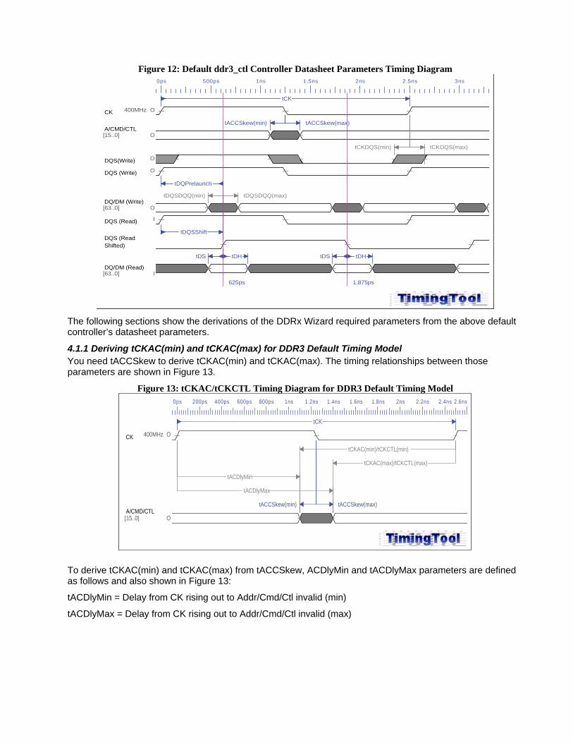
Figure 12: Default ddr3_ctl Controller Datasheet Parameters Timing Diagram 0ps 500ps 1ns 1.5ns 2ns 2.5ns 3ns
CK O400MHz
A/CMD/CTLO[15..0]
DQS(Write) O
DQS (Write) O
DQ/DM (Write)O[63..0]
DQS (Read) I
DQS (Read Shifted)
DQ/DM (Read)I[63..0]
tCK
tACCSkew(min) tACCSkew(max)
tCKDQS(min) tCKDQS(max)
tDQSShift
tDS tDH tDS tDH
tDQSDQQ(max)tDQSDQQ(min)
tDQPrelaunch
1.875ps625ps
The following sections show the derivations of the DDRx Wizard required parameters from the above default controller’s datasheet parameters.
4.1.1 Deriving tCKAC(min) and tCKAC(max) for DDR3 Default Timing Model You need tACCSkew to derive tCKAC(min) and tCKAC(max). The timing relationships between those parameters are shown in Figure 13.
Figure 13: tCKAC/tCKCTL Timing Diagram for DDR3 Default Timing Model 0ps 200ps 400ps 600ps 800ps 1ns 1.2ns 1.4ns 1.6ns 1.8ns 2ns 2.2ns 2.4ns 2.6ns
CK O400MHz
A/CMD/CTLO[15..0]
tCK
tACCSkew(min) tACCSkew(max)
tCKAC(min)/tCKCTL(min)
tCKAC(max)/tCKCTL(max)
tACDlyMin
tACDlyMax
To derive tCKAC(min) and tCKAC(max) from tACCSkew, ACDlyMin and tACDlyMax parameters are defined as follows and also shown in Figure 13:
tACDlyMin = Delay from CK rising out to Addr/Cmd/Ctl invalid (min)
tACDlyMax = Delay from CK rising out to Addr/Cmd/Ctl invalid (max)
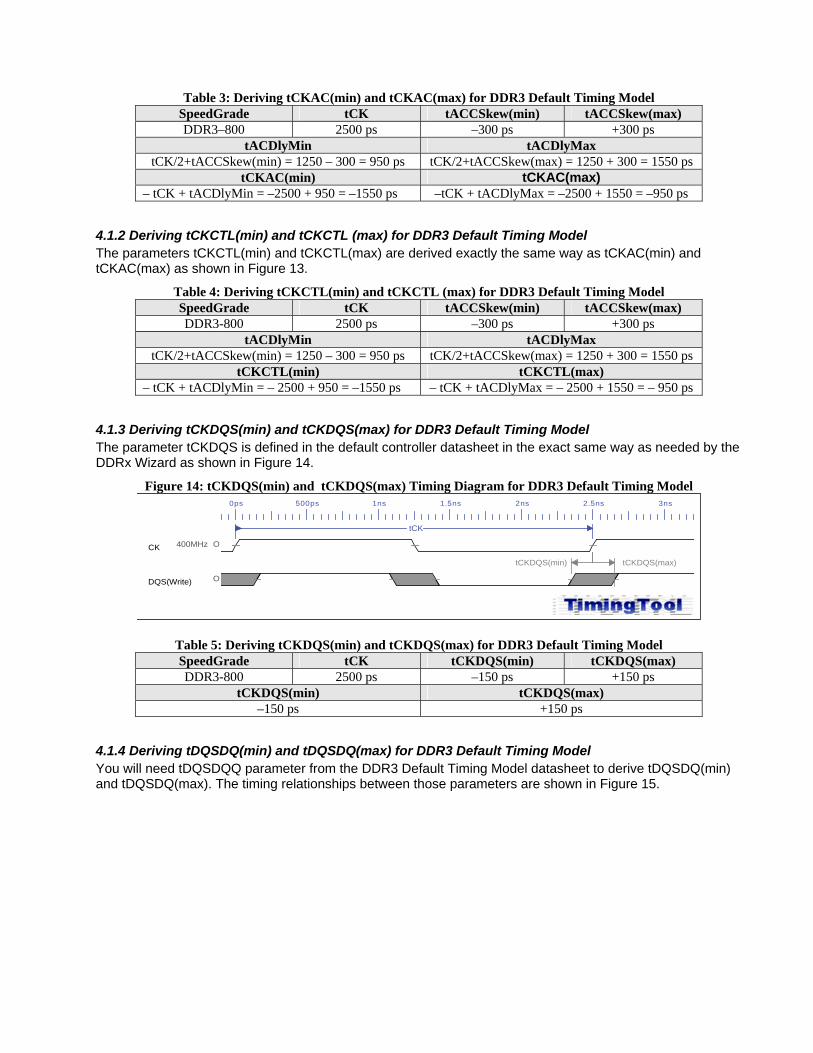
Table 3: Deriving tCKAC(min) and tCKAC(max) for DDR3 Default Timing Model SpeedGrade tCK tACCSkew(min) tACCSkew(max) DDR3–800 2500 ps –300 ps +300 ps
tACDlyMin tACDlyMax tCK/2+tACCSkew(min) = 1250 – 300 = 950 ps tCK/2+tACCSkew(max) = 1250 + 300 = 1550 ps
tCKAC(min) tCKAC(max) – tCK + tACDlyMin = –2500 + 950 = –1550 ps –tCK + tACDlyMax = –2500 + 1550 = –950 ps
4.1.2 Deriving tCKCTL(min) and tCKCTL (max) for DDR3 Default Timing Model The parameters tCKCTL(min) and tCKCTL(max) are derived exactly the same way as tCKAC(min) and tCKAC(max) as shown in Figure 13.
Table 4: Deriving tCKCTL(min) and tCKCTL (max) for DDR3 Default Timing Model SpeedGrade tCK tACCSkew(min) tACCSkew(max) DDR3-800 2500 ps –300 ps +300 ps
tACDlyMin tACDlyMax tCK/2+tACCSkew(min) = 1250 – 300 = 950 ps tCK/2+tACCSkew(max) = 1250 + 300 = 1550 ps
tCKCTL(min) tCKCTL(max) – tCK + tACDlyMin = – 2500 + 950 = –1550 ps – tCK + tACDlyMax = – 2500 + 1550 = – 950 ps
4.1.3 Deriving tCKDQS(min) and tCKDQS(max) for DDR3 Default Timing Model The parameter tCKDQS is defined in the default controller datasheet in the exact same way as needed by the DDRx Wizard as shown in Figure 14.
Figure 14: tCKDQS(min) and tCKDQS(max) Timing Diagram for DDR3 Default Timing Model 0ps 500ps 1ns 1.5ns 2ns 2.5ns 3ns
CK O400MHz
DQS(Write) O
tCK
tCKDQS(min) tCKDQS(max)
Table 5: Deriving tCKDQS(min) and tCKDQS(max) for DDR3 Default Timing Model SpeedGrade tCK tCKDQS(min) tCKDQS(max) DDR3-800 2500 ps –150 ps +150 ps
tCKDQS(min) tCKDQS(max) –150 ps +150 ps
4.1.4 Deriving tDQSDQ(min) and tDQSDQ(max) for DDR3 Default Timing Model You will need tDQSDQQ parameter from the DDR3 Default Timing Model datasheet to derive tDQSDQ(min) and tDQSDQ(max). The timing relationships between those parameters are shown in Figure 15.
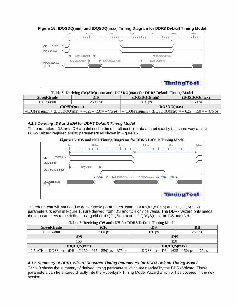
Figure 15: tDQSDQ(min) and tDQSDQ(max) Timing Diagram for DDR3 Default Timing Model
Table 6: Deriving tDQSDQ(min) and tDQSDQ(max) for DDR3 Default Timing Model
SpeedGrade tCK tDQSDQQ(min) tDQSDQQ(max) DDR3-800 2500 ps –150 ps +150 ps
tDQSDQ(min) tDQSDQ(max) –tDQPrelaunch + tDQSDQQ(min) = –625 – 150 = –775 ps – tDQPrelaunch + tDQSDQQ(max) = – 625 + 150 = – 475 ps
0ps 500ps 1ns 1.5ns 2ns 2.5ns 3ns
CK O400MHz
DQS (Write) O
DQ/DM (Write)O[63..0]
DQS (Read Shifted)
tCK
tDQSDQQ(max)tDQSDQQ(min)
tDQSDQ(max)
tDQSDQ(min)
tDQPrelaunch
4.1.5 Deriving tDS and tDH for DDR3 Default Timing Model The parameters tDS and tDH are defined in the default controller datasheet exactly the same way as the DDRx Wizard required timing parameters as shown in Figure 16.
Figure 16: tDS and tDH Timing Diagrams for DDR3 Default Timing Model 0ps 500ps 1ns 1.5ns 2ns 2.5ns
CK O400MHz
DQS (Read) I
DQS (Read Shifted)I
DQ/DM (Read)I[63..0]
tCK
tDQSShift
tDS tDH tDS tDHtDQDQS(max)tDQDQS(min)
Therefore, you will not need to derive these parameters. Note that tDQDQS(min) and tDQDQS(max) parameters (shown in Figure 16) are derived from tDS and tDH or vice versa. The DDRx Wizard only needs those parameters to be defined using either tDQDQS(min) and tDQDQS(max) or tDS and tDH.
Table 7: Deriving tDS and tDH for DDR3 Default Timing Model SpeedGrade tCK tDS tDH DDR3-800 2500 ps 150 ps 250 ps
tDS tDH 150 150
tDQDQS(min) tDQDQS(max) 0.5*tCK – tDQSShift – tDH = (1250 – 625 – 250) ps = 375 ps tDQSShift – tDS = (625 – 150) ps = 475 ps
4.1.6 Summary of DDRx Wizard Required Timing Parameters for DDR3 Default Timing Model Table 8 shows the summary of derived timing parameters which are needed by the DDRx Wizard. These parameters can be entered directly into the HyperLynx Timing Model Wizard which will be covered in the next section.
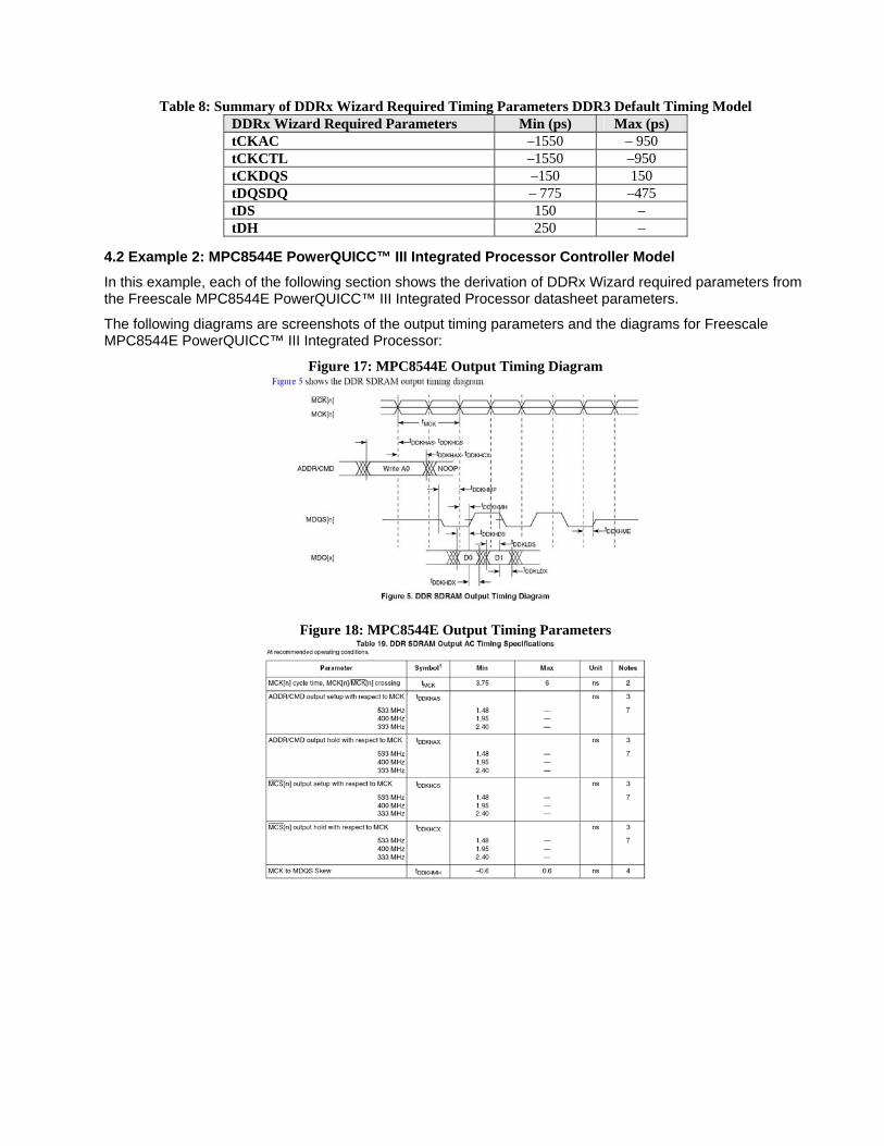
Table 8: Summary of DDRx Wizard Required Timing Parameters DDR3 Default Timing Model DDRx Wizard Required Parameters Min (ps) Max (ps) tCKAC –1550 – 950 tCKCTL –1550 –950 tCKDQS –150 150 tDQSDQ – 775 –475 tDS 150 – tDH 250 –
4.2 Example 2: MPC8544E PowerQUICC™ III Integrated Processor Controller Model
In this example, each of the following section shows the derivation of DDRx Wizard required parameters from the Freescale MPC8544E PowerQUICC™ III Integrated Processor datasheet parameters.
The following diagrams are screenshots of the output timing parameters and the diagrams for Freescale MPC8544E PowerQUICC™ III Integrated Processor:
Figure 17: MPC8544E Output Timing Diagram
Figure 18: MPC8544E Output Timing Parameters

MPC8544E Output Timing Parameters (Cont.)
4.2.1 Deriving tCKAC(min) and tCKAC(max) for MPC8544E Figure 17 and Figure 18 shows that the needed timing parameters to derive tCKAC(min)/(max) are tDDKHAS and tDDKHAX.
In this derivation, the 533MHz case will be used. Note that the 533MHz in this case is not the frequency of the clock but it is rather the speed grade for the DDRx interface. The actual frequency of the clock is half of 533MHz which is equal to 267MHz.
From the definition of tDDKHAS and tDDKHAX, they are specified as output setup and hold parameters. As you will recall from section 3.1, tCKAC(min) and tCKAC(max) parameters are defined as delay between the address and command output signals, transitioning to "valid" before the rising edge of the output clock.
Figure 19 shows the relationship between the DDRx Wizard needed parameters tCKAC(min)/(max) and the datasheet parameters (tDDKHAS and tDDKHAX). Table 9 shows the needed derivations.
Figure 19: Relationship Between tCKAC (min)/tCKAC(max) and tDDKHAS/tDDKHAX
0ps 1ns 2ns 3ns 4ns 5ns
CKO266.52452MHz
ADDR/CMDO[15..0]
tCKAC(min)
tCKAC(max)
tDDKHAS tDDKHAXtDDKHAX
tCK
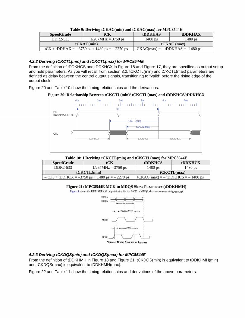
Table 9: Deriving tCKAC(min) and tCKAC(max) for MPC8544E SpeedGrade tCK tDDKHAS tDDKHAX DDR2-533 1/267MHz = 3750 ps 1480 ps 1480 ps
tCKAC(min) tCKAC (max) – tCK + tDDHAX = – 3750 ps + 1480 ps = – 2270 ps tCKAC(max) = – tDDKHAS = –1480 ps
4.2.2 Deriving tCKCTL(min) and tCKCTL(max) for MPC8544E From the definition of tDDKHCS and tDDKHCX in Figure 18 and Figure 17, they are specified as output setup and hold parameters. As you will recall from section 3.2, tCKCTL(min) and tCKCTL(max) parameters are defined as delay between the control output signals, transitioning to "valid" before the rising edge of the output clock.
Figure 20 and Table 10 show the timing relationships and the derivations.
Figure 20: Relationship Between tCKCTL(min)/ tCKCTL(max) and tDDKHCS/tDDKHCX
0ps 1ns 2ns 3ns 4ns 5ns
CKO266.52452MHz
CTL O
tCKCTL(min)
tCKCTL(max)
tDDKHCS tDDKHCXtDDKHCX
tCK
Table 10: 1 Deriving tCKCTL(min) and tCKCTL(max) for MPC8544E SpeedGrade tCK tDDKHCS tDDKHCX DDR2-533 1/267MHz = 3750 ps 1480 ps 1480 ps
tCKCTL(min) tCKCTL(max) – tCK + tDDHCX = –3750 ps + 1480 ps = – 2270 ps tCKAC(max) = – tDDKHCS = – 1480 ps
Figure 21: MPC8544E MCK to MDQS Skew Parameter (tDDKHMH)
4.2.3 Deriving tCKDQS(min) and tCKDQS(max) for MPC8544E From the definition of tDDKHMH in Figure 18 and Figure 21, tCKDQS(min) is equivalent to tDDKHMH(min) and tCKDQS(max) is equivalent to tDDKHMH(max).
Figure 22 and Table 11 show the timing relationships and derivations of the above parameters.
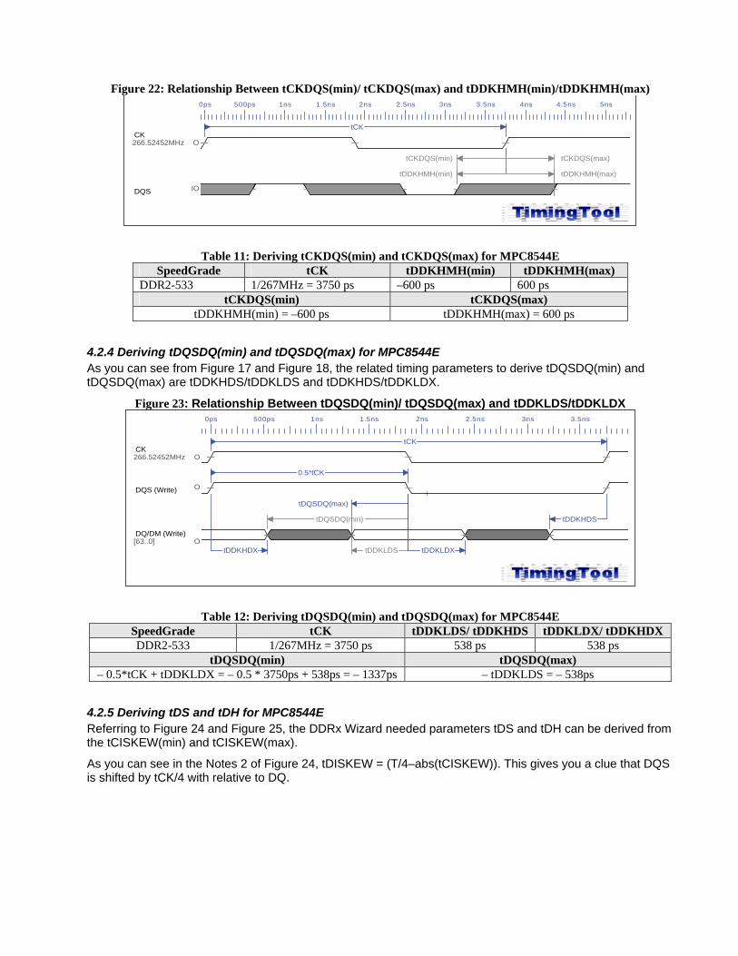
Figure 22: Relationship Between tCKDQS(min)/ tCKDQS(max) and tDDKHMH(min)/tDDKHMH(max) 0ps 500ps 1ns 1.5ns 2ns 2.5ns 3ns 3.5ns 4ns 4.5ns 5ns
CKO266.52452MHz
DQS IO
tCK
tCKDQS(min) tCKDQS(max)
tDDKHMH(min) tDDKHMH(max)
Table 11: Deriving tCKDQS(min) and tCKDQS(max) for MPC8544E SpeedGrade tCK tDDKHMH(min) tDDKHMH(max)
DDR2-533 1/267MHz = 3750 ps –600 ps 600 ps tCKDQS(min) tCKDQS(max)
tDDKHMH(min) = –600 ps tDDKHMH(max) = 600 ps 4.2.4 Deriving tDQSDQ(min) and tDQSDQ(max) for MPC8544E As you can see from Figure 17 and Figure 18, the related timing parameters to derive tDQSDQ(min) and tDQSDQ(max) are tDDKHDS/tDDKLDS and tDDKHDS/tDDKLDX.
Figure 23: Relationship Between tDQSDQ(min)/ tDQSDQ(max) and tDDKLDS/tDDKLDX 0ps 500ps 1ns 1.5ns 2ns 2.5ns 3ns 3.5ns
CKO266.52452MHz
DQS (Write) O
DQ/DM (Write)O[63..0]
tCK
tDQSDQ(max)
tDQSDQ(min)
tDDKLDS tDDKLDXtDDKHDX
tDDKHDS
0.5*tCK
Table 12: Deriving tDQSDQ(min) and tDQSDQ(max) for MPC8544E SpeedGrade tCK tDDKLDS/ tDDKHDS tDDKLDX/ tDDKHDX DDR2-533 1/267MHz = 3750 ps 538 ps 538 ps
tDQSDQ(min) tDQSDQ(max) – 0.5*tCK + tDDKLDX = – 0.5 * 3750ps + 538ps = – 1337ps – tDDKLDS = – 538ps
4.2.5 Deriving tDS and tDH for MPC8544E Referring to Figure 24 and Figure 25, the DDRx Wizard needed parameters tDS and tDH can be derived from the tCISKEW(min) and tCISKEW(max).
As you can see in the Notes 2 of Figure 24, tDISKEW = (T/4–abs(tCISKEW)). This gives you a clue that DQS is shifted by tCK/4 with relative to DQ.
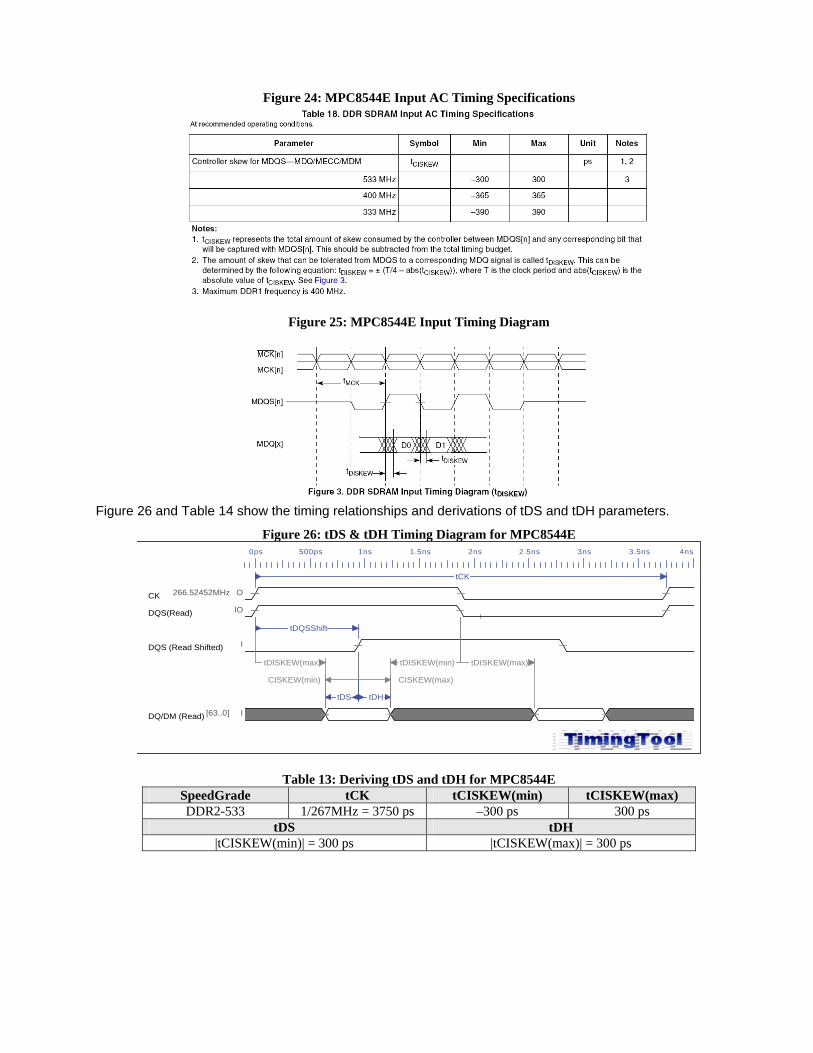
Figure 24: MPC8544E Input AC Timing Specifications
Figure 25: MPC8544E Input Timing Diagram
Figure 26 and Table 14 show the timing relationships and derivations of tDS and tDH parameters.
Figure 26: tDS & tDH Timing Diagram for MPC8544E 0ps 500ps 1ns 1.5ns 2ns 2.5ns 3ns 3.5ns 4ns
CK O266.52452MHz
DQS(Read) IO
DQS (Read Shifted) I
DQ/DM (Read) I[63..0]
tCK
tDQSShift
tDS tDH
tDISKEW(max) tDISKEW(min) tDISKEW(max)
CISKEW(min) CISKEW(max)
Table 13: Deriving tDS and tDH for MPC8544E SpeedGrade tCK tCISKEW(min) tCISKEW(max) DDR2-533 1/267MHz = 3750 ps –300 ps 300 ps
tDS tDH |tCISKEW(min)| = 300 ps |tCISKEW(max)| = 300 ps
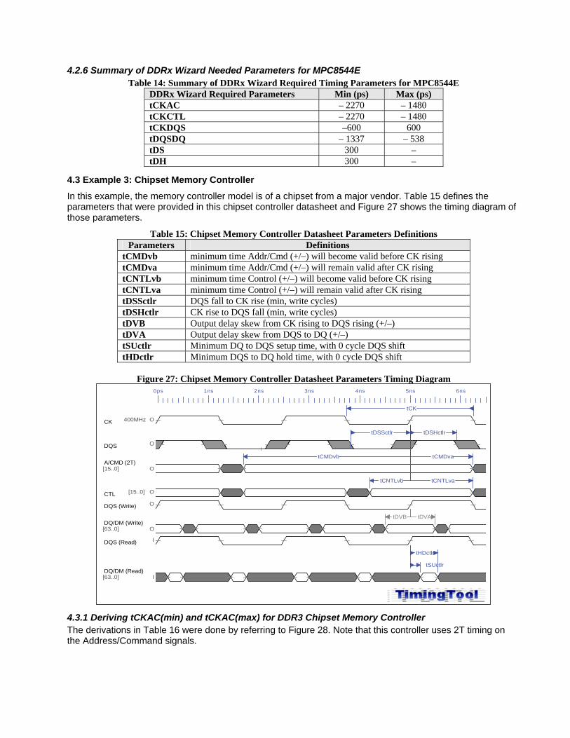
4.2.6 Summary of DDRx Wizard Needed Parameters for MPC8544E Table 14: Summary of DDRx Wizard Required Timing Parameters for MPC8544E
DDRx Wizard Required Parameters Min (ps) Max (ps) tCKAC – 2270 – 1480 tCKCTL – 2270 – 1480 tCKDQS –600 600 tDQSDQ – 1337 – 538 tDS 300 – tDH 300 –
4.3 Example 3: Chipset Memory Controller
In this example, the memory controller model is of a chipset from a major vendor. Table 15 defines the parameters that were provided in this chipset controller datasheet and Figure 27 shows the timing diagram of those parameters.
Table 15: Chipset Memory Controller Datasheet Parameters Definitions Parameters Definitions
tCMDvb minimum time Addr/Cmd (+/–) will become valid before CK rising tCMDva minimum time Addr/Cmd (+/–) will remain valid after CK rising tCNTLvb minimum time Control (+/–) will become valid before CK rising tCNTLva minimum time Control (+/–) will remain valid after CK rising tDSSctlr DQS fall to CK rise (min, write cycles) tDSHctlr CK rise to DQS fall (min, write cycles) tDVB Output delay skew from CK rising to DQS rising (+/–) tDVA Output delay skew from DQS to DQ (+/–) tSUctlr Minimum DQ to DQS setup time, with 0 cycle DQS shift tHDctlr Minimum DQS to DQ hold time, with 0 cycle DQS shift
Figure 27: Chipset Memory Controller Datasheet Parameters Timing Diagram
0ps 1ns 2ns 3ns 4ns 5ns 6ns
CK O400MHz
DQS O
A/CMD (2T)O[15..0]
CTL O[15..0]
DQS (Write) O
DQ/DM (Write)O[63..0]
DQS (Read) I
DQ/DM (Read)I[63..0]
tCMDvatCMDvb
tCNTLvatCNTLvb
tDSHctlr
tSUctlr
tHDctlr
tCK
tDSSctlr
tDVB tDVA
4.3.1 Deriving tCKAC(min) and tCKAC(max) for DDR3 Chipset Memory Controller The derivations in Table 16 were done by referring to Figure 28. Note that this controller uses 2T timing on the Address/Command signals.
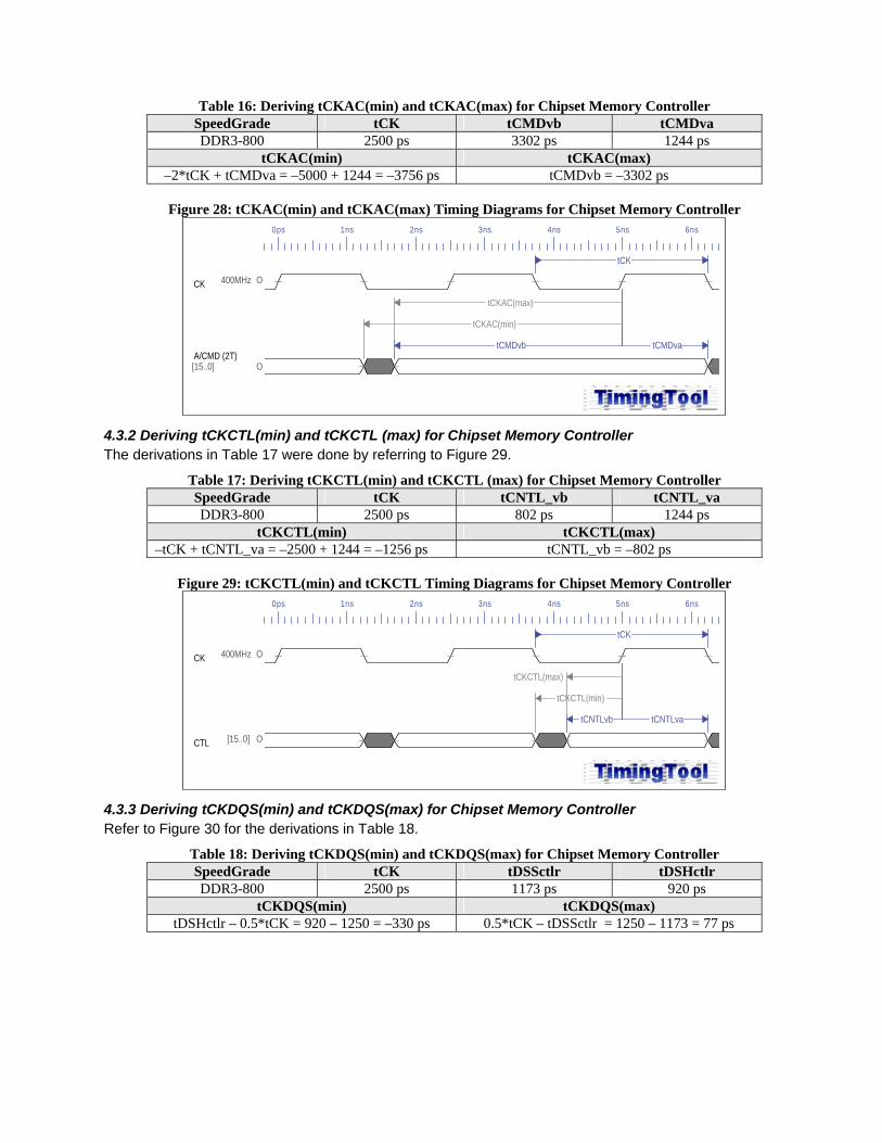
Table 16: Deriving tCKAC(min) and tCKAC(max) for Chipset Memory Controller SpeedGrade tCK tCMDvb tCMDva DDR3-800 2500 ps 3302 ps 1244 ps
tCKAC(min) tCKAC(max) –2*tCK + tCMDva = –5000 + 1244 = –3756 ps tCMDvb = –3302 ps
Figure 28: tCKAC(min) and tCKAC(max) Timing Diagrams for Chipset Memory Controller
0ps 1ns 2ns 3ns 4ns 5ns 6ns
CK O400MHz
A/CMD (2T)O[15..0]
tCMDvatCMDvb
tCK
tCKAC(max)
tCKAC(min)
4.3.2 Deriving tCKCTL(min) and tCKCTL (max) for Chipset Memory Controller The derivations in Table 17 were done by referring to Figure 29.
Table 17: Deriving tCKCTL(min) and tCKCTL (max) for Chipset Memory Controller SpeedGrade tCK tCNTL_vb tCNTL_va DDR3-800 2500 ps 802 ps 1244 ps
tCKCTL(min) tCKCTL(max) –tCK + tCNTL_va = –2500 + 1244 = –1256 ps tCNTL_vb = –802 ps
Figure 29: tCKCTL(min) and tCKCTL Timing Diagrams for Chipset Memory Controller
0ps 1ns 2ns 3ns 4ns 5ns 6ns
CK O400MHz
CTL O[15..0]
tCNTLvatCNTLvb
tCK
tCKCTL(max)
tCKCTL(min)
4.3.3 Deriving tCKDQS(min) and tCKDQS(max) for Chipset Memory Controller Refer to Figure 30 for the derivations in Table 18.
Table 18: Deriving tCKDQS(min) and tCKDQS(max) for Chipset Memory Controller SpeedGrade tCK tDSSctlr tDSHctlr DDR3-800 2500 ps 1173 ps 920 ps
tCKDQS(min) tCKDQS(max) tDSHctlr – 0.5*tCK = 920 – 1250 = –330 ps 0.5*tCK – tDSSctlr = 1250 – 1173 = 77 ps
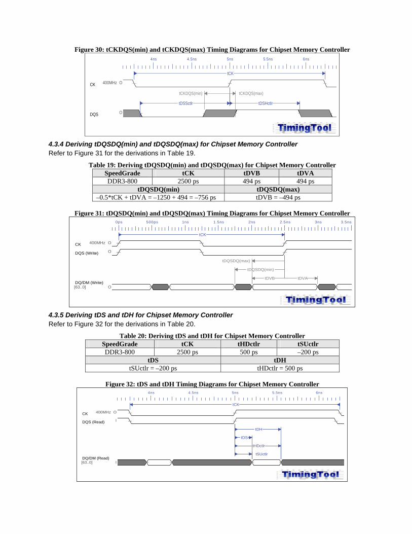
Figure 30: tCKDQS(min) and tCKDQS(max) Timing Diagrams for Chipset Memory Controller 4ns 4.5ns 5ns 5.5ns 6ns
CK O400MHz
DQS O
tDSHctlr
tCK
tDSSctlr
tCKDQS(min) tCKDQS(max)
4.3.4 Deriving tDQSDQ(min) and tDQSDQ(max) for Chipset Memory Controller Refer to Figure 31 for the derivations in Table 19.
Table 19: Deriving tDQSDQ(min) and tDQSDQ(max) for Chipset Memory Controller SpeedGrade tCK tDVB tDVA DDR3-800 2500 ps 494 ps 494 ps
tDQSDQ(min) tDQSDQ(max) –0.5*tCK + tDVA = –1250 + 494 = –756 ps tDVB = –494 ps
Figure 31: tDQSDQ(min) and tDQSDQ(max) Timing Diagrams for Chipset Memory Controller
0ps 500ps 1ns 1.5ns 2ns 2.5ns 3ns 3.5ns
CK O400MHz
DQS (Write) O
DQ/DM (Write)O[63..0]
tCK
tDQSDQ(max)
tDQSDQ(min)
tDVB tDVA
4.3.5 Deriving tDS and tDH for Chipset Memory Controller Refer to Figure 32 for the derivations in Table 20.
Table 20: Deriving tDS and tDH for Chipset Memory Controller SpeedGrade tCK tHDctlr tSUctlr DDR3-800 2500 ps 500 ps –200 ps
tDS tDH tSUctlr = –200 ps tHDctlr = 500 ps
Figure 32: tDS and tDH Timing Diagrams for Chipset Memory Controller
4ns 4.5ns 5ns 5.5ns 6ns
CK O400MHz
DQS (Read) I
DQ/DM (Read)I[63..0]
tSUctlr
tHDctlr
tCK
tDH
tDS
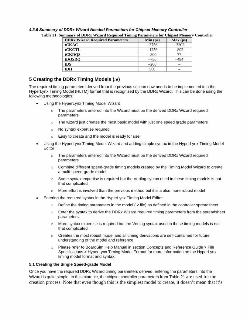
4.3.6 Summary of DDRx Wizard Needed Parameters for Chipset Memory Controller Table 21: Summary of DDRx Wizard Required Timing Parameters for Chipset Memory Controller
DDRx Wizard Required Parameters Min (ps) Max (ps) tCKAC –3756 –3302 tCKCTL –1256 –802 tCKDQS –300 77 tDQSDQ –756 –494 tDS –200 – tDH 500 –
5 Creating the DDRx Timing Models (.v) The required timing parameters derived from the previous section now needs to be implemented into the HyperLynx Timing Model (HLTM) format that is recognized by the DDRx Wizard. This can be done using the following methodologies:
• Using the HyperLynx Timing Model Wizard
o The parameters entered into the Wizard must be the derived DDRx Wizard required parameters
o The wizard just creates the most basic model with just one speed grade parameters
o No syntax expertise required
o Easy to create and the model is ready for use
• Using the HyperLynx Timing Model Wizard and adding simple syntax in the HyperLynx Timing Model Editor
o The parameters entered into the Wizard must be the derived DDRx Wizard required parameters
o Combine different speed-grade timing models created by the Timing Model Wizard to create a multi-speed-grade model
o Some syntax expertise is required but the Verilog syntax used in these timing models is not that complicated
o More effort is involved than the previous method but it is a also more robust model
• Entering the required syntax in the HyperLynx Timing Model Editor
o Define the timing parameters in the model (.v file) as defined in the controller spreadsheet
o Enter the syntax to derive the DDRx Wizard required timing parameters from the spreadsheet parameters
o More syntax expertise is required but the Verilog syntax used in these timing models is not that complicated
o Creates the most robust model and all timing derivations are self-contained for future understanding of the model and reference
o Please refer to BoardSim Help Manual in section Concepts and Reference Guide > File Specifications > HyperLynx Timing Model Format for more information on the HyperLynx timing model format and syntax.
5.1 Creating the Single Speed-grade Model
Once you have the required DDRx Wizard timing parameters derived, entering the parameters into the Wizard is quite simple. In this example, the chipset controller parameters from Table 21 are used for the creation process. Note that even though this is the simplest model to create, it doesn’t mean that it’s

less accurate. It simply means that it is the easiest and quickest to create with just one speed grade parameters. Open the HyperLynx Timing Model Wizard from BoardSim by choosing Models > Run DDRx Controller Timing Model Wizard.
5.1.1 HyperLynx Timing Model Wizard: Introduction page
.1.2 HyperLynx Timing Model Wizard: Address/Command Timing
Set the data rate for the parameters that were derived
5
Enter tCKAC (min/earliest) and tCKAC(max/latest) values. These valuare entered as positive numbers here.
es
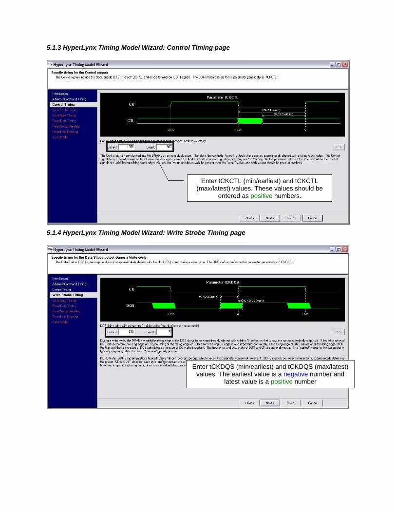
5.1.3 HyperLynx Timing Model Wizard: Control Timing page
Enter tCKCTL (min/earliest) and tCKCTL (max/latest) values. These values should be
entered as positive numbers.
5
.1.4 HyperLynx Timing Model Wizard: Write Strobe Timing page
Enter tCKDQS (min/earliest) and tCKDQS (max/latest) values. The earliest value is a negative number and
latest value is a positive number
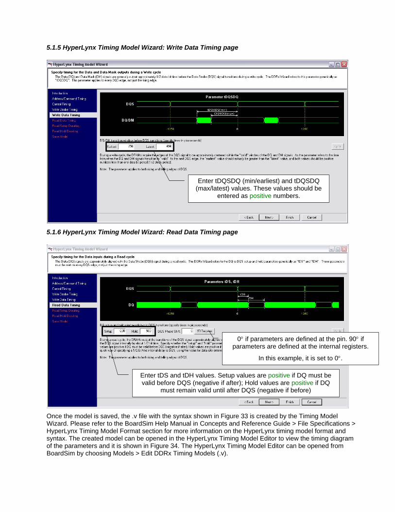
5.1.5 HyperLynx Timing Model Wizard: Write Data Timing page
5
.1.6 HyperLynx Timing Model Wizard: Read Data Timing page
Once the model is saved, the .v file with the syntax shown in Figure 33 is created by the Timing Model
ns >
Wizard. Please refer to the BoardSim Help Manual in Concepts and Reference Guide > File SpecificatioHyperLynx Timing Model Format section for more information on the HyperLynx timing model format and syntax. The created model can be opened in the HyperLynx Timing Model Editor to view the timing diagramof the parameters and it is shown in Figure 34. The HyperLynx Timing Model Editor can be opened from BoardSim by choosing Models > Edit DDRx Timing Models (.v).
Enter tDS and tDH values. Setup values are positive if DQ must be valid before DQS (negative if after); Hold values are positive if DQ
must remain valid until after DQS (negative if before)
0° if parameters are defined at the pin. 90° if p arameters are defined at the internal registers.
In this example, it is set to 0°.
Enter tDQSDQ (min/earliest) and tDQSDQ (max/latest) values. These values should be
entered as positive numbers.

Figure 33: Syntax for Single Speed-grade Chipset Controller Model Created by the Timing Model Wizard
Figure 34: Timing Diagram for the Simplest Chipset Controller Model Viewed from Timing Model Editor
Note that tCKAC(min)/(max), tCKCTL(min)/(max), and tDQSDQ(min)/(max) values were entered as positive numbers in the DDRx Timing Model Wizard but in Figure 33 and Figure 34, you will notice that those values are displayed as negative numbers. Be aware of this number convention: the DDRx Timing Model Wizard needs these numbers as positive numbers and the DDRx Wizard needs these numbers as negative numbers.
5.2 Creating Multi-Speed-grade Timing Model
This section describes the methodology to create a multi speed-grade model by combining the single speed-grade models created by the Timing Model Wizard from the previous section and adding additional simple syntax to the model.
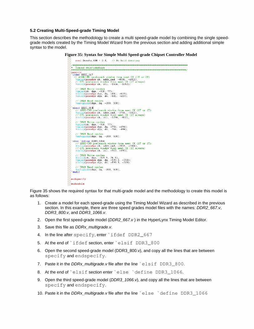
Figure 35: Syntax for Simple Multi Speed-grade Chipset Controller Model
Figure 35 shows the required syntax for that multi-grade model and the methodology to create this model is as follows:
1. Create a model for each speed-grade using the Timing Model Wizard as described in the previous section. In this example, there are three speed grades model files with the names: DDR2_667.v, DDR3_800.v, and DDR3_1066.v.
2. Open the first speed-grade model (DDR2_667.v ) in the HyperLynx Timing Model Editor.
3. Save this file as DDRx_multigrade.v.
4. In the line after specify, enter `ifdef DDR2_667
5. At the end of `ifdef section, enter `elsif DDR3_800
6. Open the second speed-grade model (DDR3_800.v), and copy all the lines that are between specify and endspecify.
7. Paste it in the DDRx_multigrade.v file after the line `elsif DDR3_800.
8. At the end of `elsif section enter `else `define DDR3_1066.
9. Open the third speed-grade model (DDR3_1066.v), and copy all the lines that are between specify and endspecify.
10. Paste it in the DDRx_multigrade.v file after the line `else `define DDR3_1066
11. At the end of `else `define section, type in `endif
12. Choose Build > Compile to check for any syntax errors.
Please refer to the BoardSim Help Manual in Concepts and Reference Guide > File Specifications > HyperLynx Timing Model Format > "Detailed Syntax - HyperLynx Timing Models" section for description of the syntax in more details.
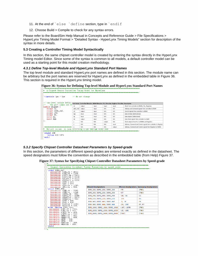
5.3 Creating a Controller Timing Model Syntactically
In this section, the same chipset controller model is created by entering the syntax directly in the HyperLynx Timing model Editor. Since some of the syntax is common to all models, a default controller model can be used as a starting point for this model creation methodology.
4.3.1 Define Top-level Module and HyperLynx Standard Port Names The top level module and standard HyperLynx port names are defined in this section. The module name can be arbitrary but the port names are reserved for HyperLynx as defined in the embedded table in Figure 36. This section is required in the HyperLynx timing model.
Figure 36: Syntax for Defining Top-level Module and HyperLynx Standard Port Names
5.3.2 Specify Chipset Controller Datasheet Parameters by Speed-grade In this section, the parameters of different speed-grades are entered exactly as defined in the datasheet. The speed designators must follow the convention as described in the embedded table (from Help) Figure 37.
Figure 37: Syntax for Specifying Chipset Controller Datasheet Parameters by Speed-grade
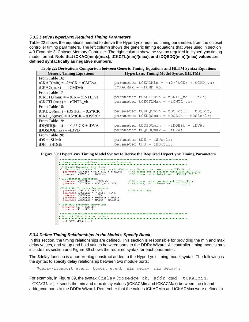
5.3.3 Derive HyperLynx Required Timing Parameters Table 22 shows the equations needed to derive the HyperLynx required timing parameters from the chipset controller timing parameters. The left column shows the generic timing equations that were used in section 4.3 Example 3: Chipset Memory Controller. The right column show the syntax required in HyperLynx timing model format. Note that tCKAC(min)/(max), tCKCTL(min)/(max), and tDQSDQ(min)/(max) values are defined syntactically as negative numbers.
Table 22: Derivations Comparison between Generic Timing Equations and HLTM Syntax Equations Generic Timing Equations HyperLynx Timing Model Syntax (HLTM)
From Table 16: tCKAC(min) = –2*tCK + tCMDva tCKAC(max) = – tCMDvb
parameter tCKACMin = –(2*`tCK) + tCMD_va; tCKACMax = –tCMD_vb;
From Table 17 tCKCTL(min) = – tCK – tCNTL_va tCKCTL(max) = –tCNTL_vb
parameter tCKCTLMin = tCNTL_va – `tCK; parameter tCKCTLMax = –tCNTL_vb;
From Table 18: tCKDQS(min) = tDSHctlr – 0.5*tCK tCKDQS(max) = 0.5*tCK – tDSSctlr
parameter tCKDQSmin = tDSHctlr – tDQBit; parameter tCKDQSmax = tDQBit – tDSSctlr;
From Table 19: tDQSDQ(min) = – 0.5*tCK + tDVA tDQSDQ(max) = –tDVB
parameter tDQSDQmin = –tDQBit + tDVA;
parameter tDQSDQmax = –tDVA; From Table 20: tDS = tSUctlr tDH = tHDctlr
parameter tDS = tSUctlr; parameter tHD = tHDctlr;
Figure 38: HyperLynx Timing Model Syntax to Derive the Required HyperLynx Timing Parameters
5.3.4 Define Timing Relationships in the Model's Specify Block In this section, the timing relationships are defined. This section is responsible for providing the min and max delay values, and setup and hold values between ports to the DDRx Wizard. All controller timing models must include this section and Figure 39 shows the required syntax for each parameter.
The $delay function is a non-Verilog construct added to the HyperLynx timing model syntax. The following is the syntax to specify delay relationship between two module ports:
$delay(fromport_event, toport_event, min_delay, max_delay);
For example, in Figure 39, the syntax $delay(posedge ck, addr_cmd, tCKACMin, tCKACMax); sends the min and max delay values (tCKACMin and tCKACMax) between the ck and addr_cmd ports to the DDRx Wizard. Remember that the values tCKACMin and tCKACMax were defined in
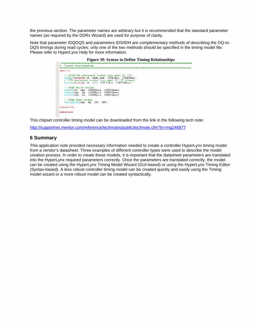
the previous section. The parameter names are arbitrary but it is recommended that the standard parameter names (as required by the DDRx Wizard) are used for purpose of clarity.
Note that parameter tDQDQS and parameters tDS/tDH are complementary methods of describing the DQ-to-DQS timings during read cycles; only one of the two methods should be specified in the timing model file. Please refer to HyperLynx Help for more information.
Figure 39: Syntax to Define Timing Relationships
This chipset controller timing model can be downloaded from the link in the following tech note:
http://supportnet.mentor.com/reference/technotes/public/technote.cfm?tn=mg246877
6 Summary This application note provided necessary information needed to create a controller HyperLynx timing model from a vendor’s datasheet. Three examples of different controller types were used to describe the model creation process. In order to create these models, it is important that the datasheet parameters are translated into the HyperLynx required parameters correctly. Once the parameters are translated correctly, the model can be created using the HyperLynx Timing Model Wizard (GUI-based) or using the HyperLynx Timing Editor (Syntax-based). A less robust controller timing model can be created quickly and easily using the Timing model wizard or a more robust model can be created syntactically.