CoreMP7 - Microsemi
30
July 2007 v2.6 1 © 2006 Actel Corporation CoreMP7 Product Summary • Personal Audio (MP3, WMA, and AAC Players) • Personal Digital Assistants • Wireless Handset • Pagers • Digital Still Camera • Inkjet/Bubble-Jet Printer • Monitors Key Features • FPGA Optimized ARM7™ Family Processor • Compatible with ARM7TDMI-S™ • 32/16-Bit RISC Architecture (ARMv4T) • 32-Bit ARM ® Instruction Set • 16-Bit Thumb ® Instruction Set • 32-Bit Unified Bus Interface • 3-Stage Pipeline • 32-Bit ALU • 32-Bit Memory Addressing Range • Static Operation • EmbeddedICE-RT™ Real-Time Debug Unit • JTAG Interface Unit Benefits • Fully Implemented in FPGA Fabric • All Microprocessor I/Os Available to User • Unified Bus Interface Simplifies SoC Design • ARM and Thumb Instruction Sets Can Be Mixed ARM Supported Families • ProASIC ® 3 (M7A3P) • Fusion (M7AFS) Synthesis and Simulation Support • Directly Supported within the Actel Libero ® Integrated Design Environment (IDE) • Synthesis: Synplify ® and Design Compiler ® • Simulation: Vital-Compliant VHDL Simulators and OVI-Compliant Verilog Simulators Verification and Compliance • Compliant with ARMv4T ISA • Compatible with ARM7TDMI-S Core Version • This Datasheet Defines the Functionality for CoreMP7 v1.0. Introduction The CoreMP7 soft IP core is an ARM7 family processor optimized for use in Actel ARM-ready FPGAs and is compatible with the ARM7TDMI-S. Users should refer to the ARM7TDM-S Technical Reference Manual (DDI0234A- 7TMIS-R4.pdf), published by the ARM Corporation, for detailed information on the ARM7. The ARM7 TRM is available for download from the ARM website at www.arm.com. CoreMP7 is supplied with an Advanced Microcontroller Bus Architecture (AMBA) Advanced High-Performance Bus (AHB) compliant wrapper for inclusion in an AMBA-based processor system such as the one generated by the Actel CoreConsole IP Deployment Platform (IDP). Contents Introduction ............................................................... 1 Device Utilization ....................................................... 2 General Description ................................................... 3 Programmer’s Model ................................................. 7 AHB Wrapper ........................................................... 12 CoreMP7 Variants ..................................................... 13 Delivery and Deployment ........................................ 14 Bus Functional Model .............................................. 14 AC Parameters .......................................................... 19 Debug ....................................................................... 23 Ordering Information .............................................. 28 List of Changes ......................................................... 28 Datasheet Categories ............................................... 29
Transcript of CoreMP7 - Microsemi

CoreMP7
Product Summary• Personal Audio (MP3, WMA, and AAC Players) • Personal Digital Assistants• Wireless Handset• Pagers• Digital Still Camera• Inkjet/Bubble-Jet Printer• Monitors
Key Features• FPGA Optimized ARM7™ Family Processor• Compatible with ARM7TDMI-S™• 32/16-Bit RISC Architecture (ARMv4T) • 32-Bit ARM® Instruction Set• 16-Bit Thumb® Instruction Set • 32-Bit Unified Bus Interface• 3-Stage Pipeline • 32-Bit ALU • 32-Bit Memory Addressing Range • Static Operation• EmbeddedICE-RT™ Real-Time Debug Unit • JTAG Interface Unit
Benefits• Fully Implemented in FPGA Fabric• All Microprocessor I/Os Available to User• Unified Bus Interface Simplifies SoC Design• ARM and Thumb Instruction Sets Can Be Mixed
ARM Supported Families • ProASIC®3 (M7A3P) • Fusion (M7AFS)
Synthesis and Simulation Support• Directly Supported within the Actel Libero®
Integrated Design Environment (IDE)• Synthesis: Synplify® and Design Compiler®
• Simulation: Vital-Compliant VHDL Simulators andOVI-Compliant Verilog Simulators
Verification and Compliance• Compliant with ARMv4T ISA• Compatible with ARM7TDMI-S
Core Version• This Datasheet Defines the Functionality for
CoreMP7 v1.0.
IntroductionThe CoreMP7 soft IP core is an ARM7 family processoroptimized for use in Actel ARM-ready FPGAs and iscompatible with the ARM7TDMI-S. Users should refer tothe ARM7TDM-S Technical Reference Manual (DDI0234A-7TMIS-R4.pdf), published by the ARM Corporation, fordetailed information on the ARM7. The ARM7 TRM isavailable for download from the ARM website atwww.arm.com.
CoreMP7 is supplied with an Advanced Microcontroller BusArchitecture (AMBA) Advanced High-Performance Bus(AHB) compliant wrapper for inclusion in an AMBA-basedprocessor system such as the one generated by the ActelCoreConsole IP Deployment Platform (IDP).
Contents
Introduction ............................................................... 1Device Utilization ....................................................... 2General Description ................................................... 3Programmer’s Model ................................................. 7AHB Wrapper ........................................................... 12CoreMP7 Variants ..................................................... 13Delivery and Deployment ........................................ 14Bus Functional Model .............................................. 14AC Parameters .......................................................... 19Debug ....................................................................... 23Ordering Information .............................................. 28List of Changes ......................................................... 28Datasheet Categories ............................................... 29
July 2007 v2.6 1© 2006 Actel Corporation

CoreMP7
ARM7 Family ProcessorCoreMP7 is a general purpose, 32-bit, ARM7 familymicroprocessor that offers high performance and lowpower consumption. The ARM architecture is based onReduced Instruction Set Computer (RISC) principles. Thesimplicity of RISC results in a high instruction throughputand fast real-time interrupt response from a small andcost-effective processor core. Pipeline techniques areemployed so that all parts of the processing and memorysystems can operate continuously. Typically, while oneinstruction is being executed, its successor is beingdecoded, and a third instruction is being fetched frommemory. The CoreMP7 processor also implements theThumb instruction set, which makes it ideally suited tohigh-volume applications with memory restrictions, orapplications where code density is an issue.
The 16-bit Thumb instruction set approaches twice thedensity of standard ARM code while retaining most ofthe ARM performance advantage over a traditional16-bit processor using 16-bit registers. This is possiblebecause Thumb code operates on the same 32-bitregister set as ARM code. Thumb code is able to reduceup to 65% of the code size compared to 32-bit ARM
instructions, and offers 160% of the performance of anequivalent ARM processor connected to a 16-bit memorysystem.
Device UtilizationCoreMP7 is available with and without debug for use ineach ARM-enabled device. These variants (Core only orCore plus debug) are available in CoreConsole and areeasily selected from the core configuration menus. Theutilization and performance of the variants for eachdevice are shown in Table 1.
Core OnlyThis variant of the CoreMP7 is optimized for maximumspeed and minimum size and does not include debug.
Core Plus DebugThis variant of the CoreMP7 is optimized for minimum
size and includes debug.
Table 1 • CoreMP7 Utilization and Performance
DeviceVariant Performance (MHz) Tiles RAM Block Utilization (%)
M7A3P1000
Core Only 28.12 6,083 4 24.8%
Core Plus Debug 21.7 7,931 4 32.3%
M7AFS600
Core Only 28.08 6,083 4 44.0%
Core Plus Debug 20.57 7,931 4 57.4%
2 v2.6

CoreMP7
General DescriptionThe CoreMP7 processor architecture, core, and functional diagrams are illustrated in the following figures:
• The CoreMP7 block diagram is shown in Figure 1.• The CoreMP7 core is shown in Figure 2 on page 4.• The CoreMP7 functional diagram is shown in Figure 3 on page 5.
Figure 1 • CoreMP7 Top-Level Block Diagram
DBGTMS
DBGnTRST
DBGTDI
DBGTDO
DBGRNG(0)DBGRNG(1)DBGEXT(0)DBGEXT(1)
WDATA[31:0]
RDATA[31:0]
CPU
DBGTCKEN
LOCKWRITE
SIZE[1:0]PROT[1:0]
TRANS[1:0]ADDR[31:0]
Scan
chai
n 1
Dat
abu
s
CoprocessorInterface Signals
EmbeddedICE-RTMacrocell
EmbeddedICE-RTTAP Controller
Scan
chai
n 2
v2.6 3

CoreMP7
Figure 2 • CoreMP7 CPU Block Diagram
CLK
CLKEN
CFGBIGEND
nIRQ
nFIQ
nRESET
ABORT
LOCK
WRITE
SIZE[1:0]
PROT[1:0]
TRANS[1:0]
DBG Outputs
DBG Input
CP Control
CP Handshake
InstructionDecoder andControl LogicShifter
ALU
Register Bank
Multiplier
Address Register
Write Data RegisterInstruction PipelineRead Data Register
Thumb Instruction Decoder
ADDR[31:0]
WDATA[31:0] RDATA[31:0]
AddressIncrementer
ALU
Bu
s
A B
us
B B
us
PC B
us Incr
emen
ter
Bu
s
4 v2.6
CoreMP7
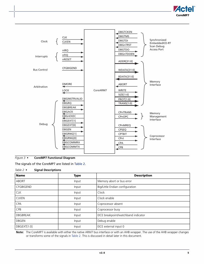
The signals of the CoreMP7 are listed in Table 2.
Figure 3 • CoreMP7 Functional Diagram
CLK
Clock
Interrupts
Bus Control
Arbitration
Debug
CLKEN
nIRQ
nFIQ
nRESET
CFGBIGEND
DMORE
LOCK
DBGINSTRVALID
DBGRQ
DBGBREAK
DBGACK
DBGnEXEC
DBGEXT[1]
DBGEXT[0]
DBGEN
DBGRNG[1]
DBGRNG[0]
DBGCOMMRX
DBGCOMMTX
DBGTCKEN
DBGTMS
DBGTDI
DBGnTRST
DBGTDO
DBGnTDOEN
ADDR[31:0]
WDATA[31:0]
RDATA[31:0]
ABORT
WRITE
SIZE[1:0]
PROT[1:0]
TRANS[1:0]
CPnTRANS
CPnOPC
CPnMREQ
CPSEQ
CPTBIT
CPnl
CPA
CPB
Synchronized EmbeddedICE-RT Scan Debug Access Port
Memory Interface
Memory Management Interface
Coprocessor Interface
CoreARM7
Table 2 • Signal Descriptions
Name Type Description
ABORT Input Memory abort or bus error
CFGBIGEND Input Big/Little Endian configuration
CLK Input Clock
CLKEN Input Clock enable
CPA Input Coprocessor absent
CPB Input Coprocessor busy
DBGBREAK Input EICE breakpoint/watchband indicator
DBGEN Input Debug enable
DBGEXT[1:0] Input EICE external input 0
Note: The CoreMP7 is available with either the native ARM7 bus interface or with an AHB wrapper. The use of the AHB wrapper changesor transforms some of the signals in Table 2. This is discussed in detail later in this document.
v2.6 5

CoreMP7
DBGnTRST Input Test reset
DBGRQ Input Debug request
DBGTCKEN Input Test clock enable
DBGTDI Input EICE data in
DBGTMS Input EICE mode select
nFIQ Input Interrupt request
nIRQ Input Fast interrupt request
nRESET Input Reset
RDATA[31:0] Input Read data bus
ADDR[31:0] Output Address bus
CPnI Output Coprocessor instruction (asserted low)
CPnMREQ Output Memory request (asserted low)
CPnOPC Output Opcode fetch (asserted low)
CPnTRANS Output Memory translate (asserted low)
CPSEQ Output Sequential address
CPTBIT Output Processor in Thumb mode
DBGACK Output Debug acknowledge
DBGCOMMRX Output EICE communication channel receive
DBGCOMMTX Output EICE communication channel transmit
DBGnEXEC Output Executed (asserted low)
DBGnTDOEN Output TDO enable (asserted low)
DBGRNG[1:0] Output EICE rangeout
DBGTDO Output EICE data out
DBGINSTRVALID Output ETM Instruction valid indicator
DMORE Output Set when next data memory access is followed by a sequential datamemory access
LOCK Output Locked transaction operation
PROT[1:0] Output Indicates code, data, or privilege level
SIZE[1:0] Output Memory access width
TRANS Output Next transaction type (i, n, s)
WDATA[31:0] Output Write data bus
WRITE Output Indicates write access
Table 2 • Signal Descriptions (Continued)
Name Type Description
Note: The CoreMP7 is available with either the native ARM7 bus interface or with an AHB wrapper. The use of the AHB wrapper changesor transforms some of the signals in Table 2. This is discussed in detail later in this document.
6 v2.6

CoreMP7
Programmer’s ModelThis section summarizes the programmer’s model of theCoreMP7. Supporting detail is available in the ARMARM7TDMI-S Technical Reference Manual (available fordownload at www.arm.com) and the ARM ArchitectureReference Manual, which can be purchased atwww.amazon.com.
The CoreMP7 processor implements the ARMv4Tarchitecture and includes both the 32-bit ARMinstruction set and the 16-bit Thumb instruction set.
Processor Operating StatesThe CoreMP7 processor has two operating states:
ARM state: 32-bit, word-aligned ARM instructions areexecuted in this state.
Thumb state: 16-bit, halfword-aligned Thumb instructionsare executed in this state.
In Thumb state, the Program Counter (PC) uses bit 1 toselect between alternate halfwords.
Note: Transition between ARM and Thumb states doesnot affect the processor mode or the register contents.
Switching StateYou can switch the operating state of the CoreMP7between ARM state and Thumb state using the BXinstruction. This is described fully in the ARMArchitecture Reference Manual.
All exception handling is performed in ARM state. If anexception occurs in Thumb state, the processor reverts toARM state. The transition back to Thumb state occursautomatically on return.
Memory FormatsThe CoreMP7 processor views memory as a linearcollection of bytes, numbered in ascending order fromzero:
• Bytes 0 to 3 hold the first stored word. • Bytes 4 to 7 hold the second stored word. • Bytes 8 to 11 hold the third stored word.
Although both Little Endian and Big Endian memoryformats are supported, it is recommended that you useLittle Endian format.
Data TypesThe CoreMP7 processor supports the following datatypes:
• Word (32-bit) • Halfword (16-bit) • Byte (8-bit)
You must align these as follows:
• Word quantities must be aligned to four-byteboundaries.
• Halfword quantities must be aligned to two-byteboundaries.
• Byte quantities can be placed on any byteboundary.
Operating ModesThe CoreMP7 processor has seven operating modes:
• User mode is the usual ARM program executionstate, and is used for executing most applicationprograms.
• Fast interrupt (FIQ) mode supports a data transferor channel process.
• Interrupt (IRQ) mode is used for general-purposeinterrupt handling.
• Supervisor mode is a protected mode for theoperating system.
• Abort mode is entered after a data or instructionprefetch abort.
• System mode is a privileged user mode for theoperating system.
• Undefined mode is entered when an undefinedinstruction is executed.
Modes other than User mode are collectively known asprivileged modes. Privileged modes are used to serviceinterrupts or exceptions, or to access protected resources.
RegistersThe CoreMP7 processor has a total of 37 registers:
• 31 general-purpose 32-bit registers • 6 status registers
These registers are not all accessible at the same time.The processor state and operating mode determinewhich registers are available to the programmer.
The ARM State Register SetIn ARM state, 16 general registers and one or two statusregisters are accessible at any one time. In privilegedmodes, mode-specific banked registers become available.Figure 4 on page 8 shows which registers are available ineach mode.
The ARM state register set contains 16 directly accessibleregisters, r0 to r15. An additional register, the CurrentProgram Status Register (CPSR), contains condition codeflags, and the current mode bits. Registers r0 to r13 aregeneral-purpose registers used to hold either data oraddress values. Registers r14 and r15 have specialfunctions as the Link Register and Program Counter.
v2.6 7

CoreMP7
Link RegisterRegister 14 is used as the subroutine Link Register(LR).
Register 14 (r14) receives a copy of r15 when a Branchwith Link (BL) instruction is executed.
At all other times, you can treat r14 as a general-purpose register.
The corresponding banked registers—r14_svc,r14_irq, r14_fiq, r14_abt, and r14_und—are similarlyused to hold the return values of r15 when interruptsand exceptions arise, or when BL instructions areexecuted within interrupt or exception routines.
Program Counter Register 15 holds the Program Counter (PC).
In ARM state, bits [1:0] of r15 are zero. Bits [31:2]contain the PC.
In Thumb state, bit [0] is zero. Bits [31:1] contain the PC.
In privileged modes, another register, the Saved ProgramStatus Register (SPSR), is accessible. This contains thecondition code flags, and the mode bits saved as a resultof the exception that caused entry to the current mode.
Figure 4 shows the ARM state registers.
Figure 4 • CoreMP7 Register Organization in the ARM State
ARM State General Registers and Program Counter
ARM State Program Status Registers
r0
r1
r2
r3
r4
r5
r6
r7
r8
r9
r10
r11
r12
r13
r14
r15 (PC)
= banked register
CPSR
r0
r1
r2
r3
r4
r5
r6
r7
r8_fiq
r9_fiq
r10_fiq
r11_fiq
r12_fiq
r13_fiq
r14_fiq
r15 (PC)
CPSR
SPSR_fiq
r0
r1
r2
r3
r4
r5
r6
r7
r8
r9
r10
r11
r12
r13_svc
r14_svc
r15 (PC)
CPSR
SPSR_svc
r0
r1
r2
r3
r4
r5
r6
r7
r8
r9
r10
r11
r12
r13_abt
r14_abt
r15 (PC)
CPSR
SPSR_abt
r0
r1
r2
r3
r4
r5
r6
r7
r8
r9
r10
r11
r12
r13_irq
r14_irq
r15 (PC)
CPSR
SPSR_irq
r0
r1
r2
r3
r4
r5
r6
r7
r8
r9
r10
r11
r12
r13_und
r14_und
r15 (PC)
CPSR
SPSR_und
System and User FIQ Supervisor Abort IRQ Undefined
8 v2.6
CoreMP7
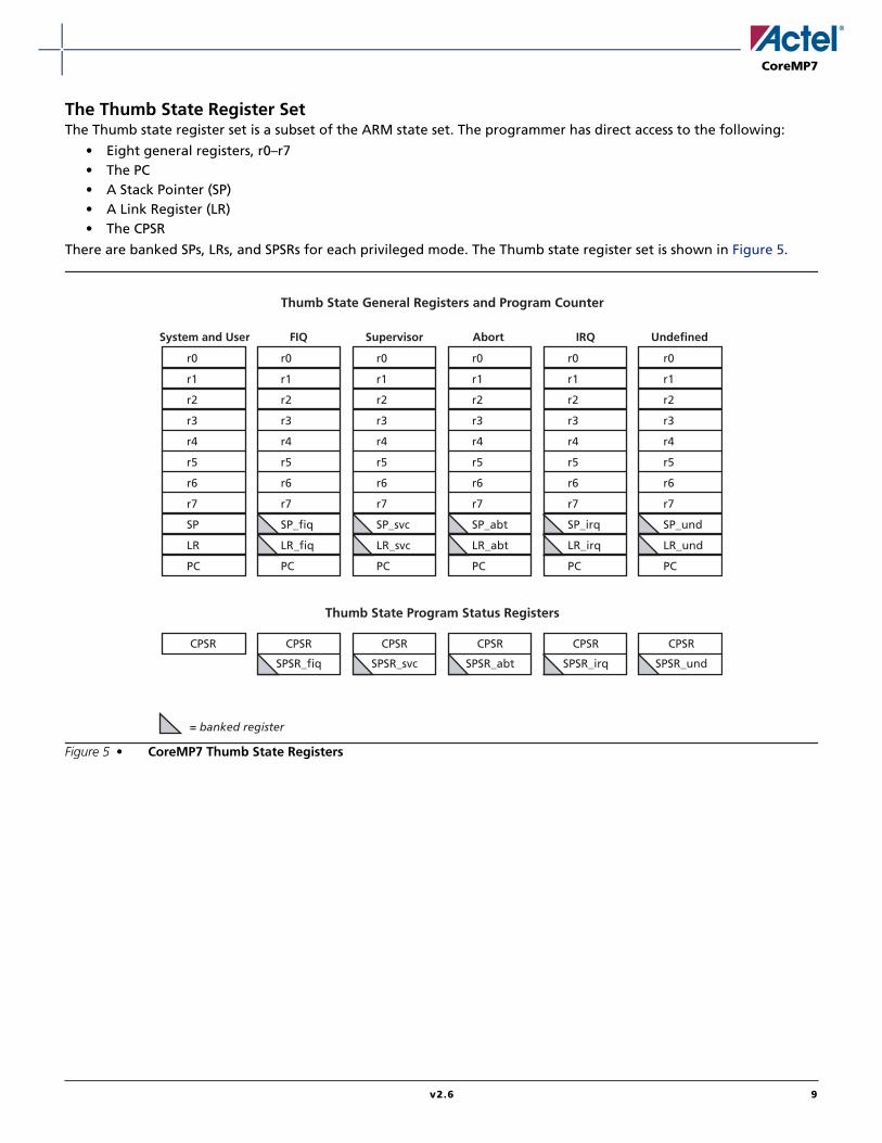
The Thumb State Register SetThe Thumb state register set is a subset of the ARM state set. The programmer has direct access to the following:
• Eight general registers, r0–r7 • The PC • A Stack Pointer (SP) • A Link Register (LR) • The CPSR
There are banked SPs, LRs, and SPSRs for each privileged mode. The Thumb state register set is shown in Figure 5.
Figure 5 • CoreMP7 Thumb State Registers
Thumb State General Registers and Program Counter
Thumb State Program Status Registers
r0
r1
r2
r3
r4
r5
r6
r7
SP
LR
PC
r0
r1
r2
r3
r4
r5
r6
r7
SP_fiq
LR_fiq
PC
r0
r1
r2
r3
r4
r5
r6
r7
SP_svc
LR_svc
PC
r0
r1
r2
r3
r4
r5
r6
r7
SP_abt
LR_abt
PC
r0
r1
r2
r3
r4
r5
r6
r7
SP_irq
LR_irq
PC
r0
r1
r2
r3
r4
r5
r6
r7
SP_und
LR_und
PC
= banked register
CPSR CPSR
SPSR_fiq
CPSR
SPSR_svc
CPSR
SPSR_abt
CPSR
SPSR_irq
CPSR
SPSR_und
System and User FIQ Supervisor Abort IRQ Undefined
v2.6 9

CoreMP7
The Relationship Between ARM State and Thumb State RegistersThe Thumb state registers relate to the ARM state registers in the following way:
• Thumb state r0–r7 and ARM state r0–r7 are identical. • Thumb state CPSR and SPSR, and ARM state CPSR and SPSR are identical. • Thumb state SP maps onto ARM state r13. • Thumb state LR maps onto ARM state r14. • The Thumb state PC maps onto the ARM state PC (r15).
These relationships are shown in Figure 6.
Note: Registers r0–r7 are known as the low registers. Registers r8–r15 are known as the high registers.
Figure 6 • Mapping of Thumb State Registers to ARM State Registers
Thumb State
r0
r1
r2
r3
r4
r5
r6
r7
r8
r9
r10
r11
r12
Stack Pointer (r13)
Link Register (r14)
Program Counter (r15)
Current Program Status Register (CPSR)
Saved Program Status Register (SPSR)
r0
r1
r2
r3
r4
r5
r6
r7
Stack Pointer (PC)
Link Register (LR)
Program Counter (PC)
Current Program Status Register (CPSR)
Saved Program Status Register (SPSR)
ARM State
10 v2.6

CoreMP7
The Program Status RegistersThe CoreMP7 core contains a CPSR and five SPSRs for exception handlers to use. The program status registers thefollowing:
• Hold the condition code flags • Control the enabling and disabling of interrupts • Set the processor operating mode
The arrangement of bits is shown in Figure 7.
The Condition Code FlagsThe N, Z, C, and V bits are the condition code flags. You can set these bits by arithmetic and logical operations. Theflags can also be set by MSR and LDM instructions. The CoreMP7 processor tests these flags to determine whether toexecute an instruction.
All instructions can be executed conditionally in ARM state. In Thumb state, only the Branch instruction can beexecuted conditionally. For more information about conditional execution, see the ARM Architecture ReferenceManual.
Figure 7 • Program Status Register Format
Condition Code Flags Reserved Control Bits
Overflow
ZeroNegative or Less Than
Mode BitsState BitFIQ DisableIRQ Disable
31 30 29 28
N Z C V
27 26 25 24 23 8 7 6 5 4 3 2 1 0
I F T M4 M3 M2 M1 M0
Carry or Borrow or Extend
v2.6 11
CoreMP7
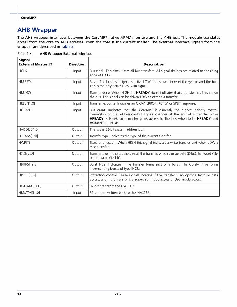
AHB WrapperThe AHB wrapper interfaces between the CoreMP7 native ARM7 interface and the AHB bus. The module translatesaccess from the core to AHB accesses when the core is the current master. The external interface signals from thewrapper are described in Table 3.
Table 3 • AHB Wrapper External Interface
SignalExternal Master I/F Direction Description
HCLK Input Bus clock. This clock times all bus transfers. All signal timings are related to the risingedge of HCLK.
HRESETn Input Reset. The bus reset signal is active LOW and is used to reset the system and the bus.This is the only active LOW AHB signal.
HREADY Input Transfer done. When HIGH the HREADY signal indicates that a transfer has finished onthe bus. This signal can be driven LOW to extend a transfer.
HRESP[1:0] Input Transfer response. Indicates an OKAY, ERROR, RETRY, or SPLIT response.
HGRANT Input Bus grant. Indicates that the CoreMP7 is currently the highest priority master.Ownership of the address/control signals changes at the end of a transfer whenHREADY is HIGH, so a master gains access to the bus when both HREADY andHGRANT are HIGH.
HADDR[31:0] Output This is the 32-bit system address bus.
HTRANS[1:0] Output Transfer type. Indicates the type of the current transfer.
HWRITE Output Transfer direction. When HIGH this signal indicates a write transfer and when LOW aread transfer.
HSIZE[2:0] Output Transfer size. Indicates the size of the transfer, which can be byte (8-bit), halfword (16-bit), or word (32-bit).
HBURST[2:0] Output Burst type. Indicates if the transfer forms part of a burst. The CoreMP7 performsincrementing bursts of type INCR.
HPROT[3:0] Output Protection control. These signals indicate if the transfer is an opcode fetch or dataaccess, and if the transfer is a Supervisor mode access or User mode access.
HWDATA[31:0] Output 32-bit data from the MASTER.
HRDATA[31:0] Input 32-bit data written back to the MASTER.
12 v2.6

CoreMP7
CoreMP7 VariantsThere are two implementations of CoreMP7 (Core Only and Core Plus Debug). The utilization and performance of thevariants are shown in Table 1 on page 2.
Core Plus DebugThe Core Plus Debug variant is configured with allfeatures of the ARM7TDMI-S. The variant incorporatesthe full debug functionality of the ARM7TDMI-S and isfully compliant with RealView RVDS, RVDK, and otherARM software debug tools.
Core OnlyThe Core Only variant has the same features as the CorePlus Debug variant except that it does not include theICE-RT debug block or the TAP controller, which reducesthe size of the core. This means that the standard debugtools cannot be used with this variant of CoreMP7.
No DebugThis is the most obvious characteristic of the Core Onlyvariant. To reduce area, the Debug EmbeddedICE-RTmacrocell, the EmbeddedICE-RT TAP controller, and thescan logic have been optimized out. This means thatstandard software debug tools cannot be used when thisvariant of the CoreMP7 is instantiated. Users can employthe Core Plus Debug variant for development, and whenthe application has been fully tested and debugged, theCore Only variant can be instantiated to reduce area inthe final shipping product.
No Coprocessor InterfaceThe coprocessor interface is a rarely used feature inARM7 family microprocessors and has been removedfrom CoreMP7 to minimize area.
Little Endian OnlyMost microprocessor-based systems use Little Endianbyte ordering. The option of selecting Big Endian hasbeen removed from CoreMP7 to minimize area.
On-Chip RAM Consumed by Register BlockTo minimize the area, the CoreMP7 variants map theprocessor register block into on-chip RAM. RAM blocksused to implement CoreMP7 registers are no longeravailable for use in user designs.
Figure 8 • ARM7 TDMI-S Core
ARM7 CPUCoprocessor
Signals
Data
Address
Bus ControlSignals
Debug InterfaceDebug JTAG
Signals
ARM7TDMI-S Core
Debug
EmbeddedICE-RT(Debug)
TAPController
v2.6 13

CoreMP7
Delivery and DeploymentThe CoreMP7 is delivered in CoreConsole, and can beinstantiated in design projects created in Libero IDE. Thefiles included with CoreMP7 consist of the Bus FunctionalModel (BFM) files and test wrapper, AHB wrapper, andthe A7S secured CDB file. The A7S secured CDB file isinstantiated on the user device at programming. Thisdeployment flow is implemented to ensure that thedesign is kept completely secure at all times, and allowsCoreMP7 to be easily used with the standard design flowthrough the Libero IDE tool suite.
Bus Functional ModelDuring the development of an FPGA-based SoC, anumber of stages of testing may be undertaken. This caninvolve some, or all, of the following approaches:
• Hardware simulation, using Verilog or VHDL • Software simulation, using a host-based
instruction set simulator (ISS) of the SoC'sprocessor
• Hardware and software co-verification, using afully functional model of the processor in Verilog,VHDL, or SWIFT form, or using a tool such asSeamless
Due to the rapid prototyping capability of FPGAs,however, integration of hardware and software oftenoccurs earlier in the SoC development cycle for FPGAtargets than it would for ASIC targets. Therefore,hardware and software co-verification, which can bevery slow, is not a critical issue except in the mostcomplex FPGA-based SoCs.
The planned availability of ARM-based SoC solutions toActel FPGA customers necessitates that Actel providesupport for the test approaches described above. Inparticular, there should be an emphasis on providingsolutions for hardware simulation and for softwaresimulation.
A software simulation solution is already available tocustomers as part of the proposed ARM package. Thispackage contains the RealView Instruction Set Simulator,which provides ARM7 instruction accurate simulation, aswell as powerful features, such as integration with theRealView debugger.
Support for hardware simulation is also proposed. TheCoreConsole SoC configuration utility provides a meansfor the developer to stitch together IP blocks using a busfabric of choice. It generates a system testbench,controlled by a script-driven, bus functional model (BFM)of the ARM7 processor. The ARM7 BFM allows thedeveloper to model low-level bus transactions, whichallow verification of connectivity of the various IP blocks
and the system memory map presented to the ARM7 bythe rest of the hardware.
This document specifies the following aspects of theARM7 BFM:
• Functionality• BFM usage flow• BFM script language• Platforms• Supported simulation tools• Example BFM use case
BFM Usage FlowAs the BFM is part of an overall system test strategy, it ishelpful to look at the context in which it is used. Figure 9on page 15 shows the various components within anexample system-level testbench that can be generated byCoreConsole.
In Figure 9 on page 15, it is assumed that the developerspecifies an SoC subsystem by selecting the processor, busfabric, IP blocks, and memory subsystem in CoreConsole.In this example, the user selects the following:
• ARM7 processor, • AMBA AHB bus fabric • MAC 10/100 IP core • CoreUART IP core • External SSRAM and Flash memory
As a result of constructing the CoreConsole subsystem,the memory map for the system is created. Based on thisinformation, CoreConsole generates the followingoutputs, among others:
• Verilog/VHDL model of SoC subsystem• Verilog/VHDL models of IP cores• Verilog/VHDL model of ARM7 BFM• BFM test script• System-level skeleton testbench
The BFM acts as a pin-for-pin replacement of theARM7TDMI-S in the SoC subsystem. It initiates bustransactions on the native ARM7 bus, which are cycle-accurate with real bus cycles that the ARM7TDMI-Swould produce. It has no knowledge, however, of realARM7 instructions.
At this point, the BFM may be used to run a basic test ofthe SoC subsystem using the skeleton system testbench.The BFM is fully integrated into the CoreConsole userflow. In particular, if the user has an AHB-based CoreMP7subsystem, CoreConsole automatically derives thememory map of the user's subsystem. CoreConsole usesthis information to generate an overall BFM test script,which includes customized "scriptlets" for each resourceattached to the AHB or APB buses.
14 v2.6
CoreMP7
The developer may edit the SoC Verilog/VHDL to addnew design blocks, such as the VideoCodec in the abovediagram. The system-level testbench may also be filledout by the developer to include tasks that test any newlyadded functionality or additional stubs that allow morecomplex system testing involving the IP cores. The BFMinput scripts may also be manually enhanced to allow the
user to test access to register locations in newly addedlogic. In this way, the user can provide stimuli to thesystem from the inside (via the ARM7 BFM), as well asfrom the outside (via testbench tasks).
Figure 10 shows the design flow into which the BFM fits.
Figure 9 • SoC System-Level Testbench Example
BFM TestScript
BFM Log File
ARM7 BFM
CoreUART
Video Codec
Memory Controller
ARM7-AHBBridge
SSRAM
Flash
SoC SystemTestbench
SoC Subsystem
Video Test Stub
MAC Test Stub
MAC 10/100
SoC W rapper
User-Defined
Tasks andFunction
Figure 10 • BFM Flow Diagram
Actel IP Core Attributes (SPIRIT)
User Input
BFM Log File
SoC System TestbenchBFM Test Script
Memory Map DefinitionIP Cores Selection
Bus Fabric Selection
Core Console
v2.6 15

CoreMP7
FunctionalityThis section describes the specific functionality of theARM7 BFM. The BFM models the ARM7 native bus.Specifically, this models the following bus signals:
CoreConsole v1.1ARM7 Pin CompatibilityThe BFM model is pin-for-pin compatible with theARM7TDMI-S. This allows the model to be dropped intothe space that would be occupied by the ARM in theVerilog/VHDL system testbench.
ARM7 Bus Cycle AccuracyThe bus cycle timings for the ARM7 native bus signals arespecified in the ARM7TDMI Technical Reference Manual.The BFM models these bus cycles exactly.
ScriptingIn order to provide a simple and extensible mechanismfor providing stimuli to the BFM, a BFM scriptinglanguage is defined (see the "BFM Script Language"section). The scripting language can initiate writes tosystem resources, reads from system resources (with orwithout checking of expected data), and can wait forevents.
Self-CheckingThe BFM gives a pass/fail indication at the end of a testrun. This is based on whether any of the expected dataread checks failed or not.
EndianessThe BFM supports both big and little-endian memoryconfigurations. For byte and halfword transfers, it readsand writes data from/to the appropriate data lanes.
Interrupt SupportThe BFM has the ability to wait for either of the twoARM7 interrupt lines to be triggered, before proceedingwith the remainder of the test script.
Log File GenerationThe BFM generates output messages to the console ofthe simulation tool and also generates a plain text logfile.
BFM Script LanguageThe following script commands are defined for use bythe BFM:
memmapThis command is used to associate a label, representing asystem resource, with a memory map location. The otherBFM script commands may perform accesses to locationswithin this resource by referencing this label and aregister offset relative to this base address.
Syntaxmemmap resource_name base_address;
resource_nameThis is a string containing the user-friendly instancename of the resource being accessed. For BFM scriptsgenerated automatically by CoreConsole, this namecorresponds to the instance name of the associated corein the generated subsystem Verilog or VHDL.
base_addressThis is the base address of the resource, in hexadecimal.
writeThis command causes the BFM to perform a write to aspecified offset, within the memory map range of aspecified system resource.
Syntaxwrite width resource_name byte_offset data;
widthThis takes on the enumerated values of W, H, or B, forword, halfword, or byte.
resource_nameThis is a string containing the user-friendly instancename of the resource being accessed, as defined by theuser in the memory map (when input to CoreConsole).
byte_offsetThis is the offset from the base of the resource, in bytes.It is specified as a hexadecimal value.
dataThis is the data to be written. It is specified as ahexadecimal value.
Examplewrite W videoCodec 20 11223344;
• ADDR, // address bus
• WDATA, // write data bus
• RDATA, // read data bus
• TRANS, // next transaction type (i, n, or s)
• WRITE, // indicates write access
• CLKEN, // clock enable
The BFM also models the following control signals:
• CFGBIGEND, // big/little endian configuration
• CLK, // clock
• nFIQ, // interrupt request
• nIRQ, // fast interrupt request
• SIZE, // memory access width
16 v2.6
CoreMP7
readThis command causes the BFM to perform a read of aspecified offset, within the memory map range of aspecified system resource.
Syntaxread width resource_name byte_offset;
widthThis takes on the enumerated values of W, H, or B, forword, halfword, or byte.
resource_nameThis is a string containing the user-friendly instancename of the resource being accessed, as defined by theuser in the memory map (when input to CoreConsole).
byte_offsetThis is the offset from the base of the resource, in bytes.It is specified as a hexadecimal value.
Exampleread W videoCodec 20;
readcheckThis command causes the BFM to perform a read of aspecified offset, within the memory map range of aspecified system resource, and to compare the read valuewith the expected value provided.
Syntaxreadcheck width resource_name byte_offset data;
widthThis takes on the enumerated values of W, H, or B, forword, halfword, or byte.
resource_nameThis is a string containing the user-friendly instancename of the resource being accessed, as defined by theuser in the memory map (when input to CoreConsole).
byte_offsetThis is the offset from the base of the resource, in bytes.It is specified as a hexadecimal value.
dataThis is the expected read data. It is specified as ahexadecimal value.
Examplereadcheck W videoCodec 20 11223344;
pollThis command continuously reads a specified locationuntil a requested value is obtained. This command allowsone or more bits of the read data to be masked out. Thisallows, for example, poll waiting for a ready bit to be set,while ignoring the values of the other bits in the locationbeing read.
Syntaxpoll width resource_name byte_offset data_bitmask;
widthThis takes on the enumerated values of W, H, or B, forword, halfword, or byte.
resource_nameThis is a string containing the user-friendly instancename of the resource being accessed.
byte_offsetThis is the offset from the base of the resource, in bytes.It is specified as a hexadecimal value.
bitmaskThe bitmask is ANDed with the read data and the resultis then compared to the bitmask itself. If equal, then allthe bits of interest are at their required value and thepoll command is complete. If not equal, then the pollingcontinues.
waitThis command causes the BFM script to stall for aspecified number of clock periods.
Syntaxwait num_clock_ticks;
num_clock_ticksThis is the number of CoreMP7 clock periods, duringwhich the BFM stalls (doesn't initiate any bustransactions).
waitfiqThis command causes the BFM to wait until an interruptevent (high to low transition) is seen on the nFIQ pinbefore proceeding with the execution of the remainderof the script.
Syntaxwaitfiq;
waitirqThis command causes the BFM to wait until an interruptevent (high to low transition) is seen on the nIRQ pinbefore proceeding with the execution of the remainderof the script.
Syntaxwaitirq;
Supported Simulation ToolsBFM is delivered to the user as both a Verilog and VHDLmodel.
v2.6 17
CoreMP7
Timing ShellThe BFM incorporates a timing shell, which performssetup/hold checks on inputs and delays outputs by theappropriate amount from the rising clock edge.
Example BFM Use CaseThis provides an example use case of the ARM7 BFM. Theexample SoC used in this section is the same as thatshown in Figure 9 on page 15. In this system, thedeveloper requires two Actel IP cores: the MAC 10/100and the CoreUART.
SPIRIT AttributesCoreConsole has access to a database of Actel IP coresand a list of attributes for each core. These attributes areorganized according to the SPIRIT specification, in XML.For example, in the case of the CoreUART, the attributeswould indicate that there are three registers, as inTable 4.
Based on these attributes, CoreConsole can determinethat when generating the BFM script, there are threelocations corresponding to the UART that can beaccessed. In this case, none of the registers are RW, sothere will not be any self-checking that can beperformed for the UART. Nevertheless, the bustransactions do take place and the cycles may be viewedin a waveform of the simulator.
Memory MapThe designer must feed in the memory map of the SoC toCoreConsole. During this stage, the absolute addressranges of the various system resources in the ARM7memory map are fed in. Also, user-friendly instancenames of these resources are fed in.
For example, the user could feed the memory mapinformation into CoreConsole that is given in Table 5.
Based on the information in Table 5, CoreConsolegenerates the SoC subsystem corresponding to the ActelIP cores present. It also generates a BFM script, whichaccesses all the registers in the Actel IP cores.
Processor ChoiceIn this example, the user selects an ARM7 as theprocessor of choice in CoreConsole. The BFM in thisspecification only relates to ARM7.
Bus Fabric SelectionThe user may select one of a number of bus fabrics inCoreConsole. For example, the user could select AMBAAHB-Lite. However, this selection is irrelevant for theARM7 BFM, as it is concerned only with generatingnative ARM7 bus based transactions.
Automatic BFM ScriptletAt this point, having run CoreConsole to completion, aBFM scriptlet is available. This would look something likethe following:
read B uart 0;
write B uart 4 bb;
read B uart 8;
write B mac 30 11;
readcheck B mac 11;
Run BFMThe developer can run the BFM with the automatic scriptor edit the script to put in bus transactions to/from anynew logic that has been added to the SoC. For example,transactions to/from the registers in the new VideoCodecblock could be added.
The skeleton system-level testbench, generated byCoreConsole, could also be modified, to add someexternal resources (e.g., models of SSRAM and Flash) andsome high-level tasks.
Upon running the system simulation, messages appear inthe console window of the simulation tool.
Table 4 • CoreUART Attributes
Offset Register Read/Write Width
0 Uart Status Register R Byte
1 Uart Tx data W Byte
2 Uart Rx data R Byte
Table 5 • Memory Map Information
Resource Actel IP Core Address Range
ssram N 0-3fffff
flash N 400000-7fffff
uart Y c00000-c0000b
mac Y d00000-d00040
videocodec N e00000-e000ff
18 v2.6
CoreMP7
AC ParametersThis section gives the AC timing parameters of the CoreMP7 processor.
Timing DiagramsTiming diagrams are shown in Figure 11, Figure 12 on page 20, Figure 13 on page 20, Figure 14 on page 21, andFigure 15 on page 21.
Data Access Timing
Figure 11 • Data Access Timing
CLK
TRANS[1:0] TRANS
Addr
Ctrl
Data
ADDR[31:0]
WRITE SIZE[1:0]
PROT[1:0]
WDATA[31:0] (write data)
CLKEN
ABORT
RDATA[31:0] (read data)
tovtranstohtrans
tovaddrtohaddr
tovctl tohctl
tovwdata tohwdata
tisclken
tihclken
tisabort
tihabort
tisrdata
tihrdata
v2.6 19

CoreMP7
Coprocessor TimingThe Coprocessor timing is included for completeness although it is expected that the Coprocessor interface is omittedin most deployments of the CoreMP7.
Exception Timing
Figure 12 • Coprocessor Timing
Figure 13 • Exception Timing
CLK
CPA CPB
CPnl
CPnMREQ CPSEQ
CPnOPC CPnTRANS
CPTBIT
tiscpstart
tihcpstart
tovcpni tohcpni
tovcpcil tohcpcil
tovcpcil tohcpcil
CLK
nFIQ nIRQ
nRESET
CFGBIGEND
tisexc
tihexc
tisexc
tihexc
tiscfg
tihcfg
20 v2.6

CoreMP7
Debug Timing
Scan Timing
Figure 14 • Debug Timing
CLK
DBGRQ
DBGBREAK
DBGEXT[1:0]
DBGACK DBGCOMMTX DBGCOMMRX
DBGRNG[1:0]
tisdbgctltihdbgctl
tisdbgctltihdbgctl
tisdbgctltihdbgctl
tovdbgstart tohdbgstart
tovdbgstart tohdbgstart
Figure 15 • Scan Timing
CLK
DBGTCKEN
DBGTMS DBGTDI
DBGTDO
tslcken
tlhocken
tslcil
tlhocil
tovido tohido
v2.6 21

CoreMP7
AC Timing Parameter DefinitionsTable 6 shows target AC parameters. All figures are expressed as percentages of the CLK period at maximumoperating frequency.
Note: Where 0% is shown, this indicates the hold time to clock edge plus the maximum clock skew for internal clockbuffering.
Table 6 • AC Timing Parameters
Symbol Parameter Min Max
tCYC CLK cycle time 100% –
tISCLKEN CLKEN input setup to rising CLK 60% –
tIHCLKEN CLKEN input hold from rising CLK – See notes 1, 2
tISABORT ABORT input setup to rising CLK 40% –
tIHABORT ABORT input hold from rising CLK – 0%
tISRDATA RDATA input setup to rising CLK 10% –
tISRST nRESET input setup to rising CLK 90% –
tISTRST DBGnTRST input setup to rising CLK 25%
tIHRDATA RDATA input hold from rising CLK – See notes 3, 4
tOCPTBIT Rising CLK to CPTBIT valid – 90%
tODBG Rising CLK to DBGnEXEC, DBGINSTRVALID valid – 40%
tOLOMO Rising CLK to DMORE, LOCK valid – 90%
tOVADDR Rising CLK to ADDR valid – 90%
tOHADDR ADDR hold time from rising CLK >0% –
tOVCTL Rising CLK to control valid – 90%
tOHCTL Control hold time from rising CLK >0% –
tOVTRANS Rising CLK to transaction type valid – 50%
tOHTRANS Transaction type hold time from rising CLK >0% –
tOVWDATA Rising CLK to WDATA valid – 40%
tOHWDATA WDATA hold time from rising CLK >0% –
tISCPSTAT CPA, CPB input setup to rising CLK 20% –
tIHCPSTAT CPA, CPB input hold from rising CLK – 0%
tOVCPCTL Rising CLK to coprocessor control valid – 80%
tOHCPCTL Coprocessor control hold time from rising CLK >0% –
tOVCPNI Rising CLK to coprocessor CPnI valid – 40%
tOHCPNI Coprocessor CPnI hold time from rising CLK >0% –
tISEXC nFIQ, nIRQ, input setup to rising CLK 10% –
Notes:
1. tIHCLKEN is 0 ns for the Core Plus Debug variant in all devices.2. tIHCLKEN is 1 ns for the Core Only variant in all devices.
3. tIHRDATA is 0 ns for Core Plus Debug variant in all devices.
4. tIHRDATA is 1 ns for Core Only variant in all devices.
22 v2.6

CoreMP7
DebugThe ARM Debug Architecture uses a protocol converterbox to allow the debugger to talk via a Joint Test ActionGroup (JTAG) port directly to the core. In effect, the scanchains in the core that are required for test are re-usedfor debugging.
The architecture uses the scan chains to insertinstructions directly in to the ARM core. The instructionsare executed on the core and, depending on the type ofinstruction that has been inserted, the core or the systemstate can be examined, saved, or changed. Thearchitecture has the ability to execute instructions at aslow debug speed or to execute instructions at systemspeed (for example, if access to an external memory wasrequired).
The fact that the debugger is actually using the JTAGscan chains to access the core is of no importance to theuser, as the front end debugger remains exactly thesame. The user could still use the debugger with amonitor program running on the target system or with
an instruction set simulator that runs on the debuggerhost. In each case the debugging environment is thesame.
The advantages of using the JTAG port are:
• Hardware access required by a system for test is re-used for debug.
• Core state and system state can be examined viathe JTAG port.
• The target system does not have to be running inorder to start debug.
A monitor program for example requires that sometarget resources are running in order for the monitorprogram to run.
• Traditional breakpoints and watchpoints areavailable.
• On-chip resources can be supplemented.• For example, the ARM Debug Architecture uses an
on-chip macro-cell to enhance the debuggingfacilities available.
tIHEXC nFIQ, nIRQ, nRESET hold from rising CLK – 0%
tISCFG CFGBIGEND setup to rising CLK 10% –
tIHCFG CFGBIGEND hold from rising CLK – 0%
tISDBGCTL DBGBREAK, DBGEXT, DBGRQ input setup to rising CLK 10% –
tISDBGSTAT Debug status inputs setup to rising CLK 10% –
tIHDBGSTAT Debug status inputs hold from rising CLK – 0%
tOVDBGCTL Rising CLK to debug control valid – 40%
tOHDBCTL Debug control hold time from rising CLK >0% –
tISTCLKEN DBGTCKEN input setup to rising CLK 60%‘ –
tIHTCKEN DBGTCKEN input hold from rising CLK – 0%
tISTCTL DBGTDI, DBGTMS input setup to rising CLK 35% –
tIHTCTL DBGTDI, DBGTMS input hold from rising CLK – 0%
tOVTDO Rising CLK to DBGTDO valid – 20%
tOHTDO DBGTDO hold time from rising CLK >0% –
tOVDBGSTAT Rising CLK to debug status valid 40% –
tOHDBGSTAT Debug status hold time >0% –
Table 6 • AC Timing Parameters (Continued)
Symbol Parameter Min Max
Notes:
1. tIHCLKEN is 0 ns for the Core Plus Debug variant in all devices.2. tIHCLKEN is 1 ns for the Core Only variant in all devices.
3. tIHRDATA is 0 ns for Core Plus Debug variant in all devices.
4. tIHRDATA is 1 ns for Core Only variant in all devices.
v2.6 23

CoreMP7
• A separate UART to communicate with themonitor program is not required.
The debugging of the target system requires thefollowing:
• A PC host computer running Windows to run thedebugger software
• An EmbeddedICE Protocol Converter, a separatebox which converts the serial interface to signalscompatible with the JTAG interface and a targetsystem with a JTAG interface and an ARM DebugArchitecture compliant core.
Once the system is connected, the debugger can startcommunicating with the target system via the RVI-ME(which is an EmbeddedICE Interface Converter).
The debug extensions consist of several scan chainsaround the processor core, and some additional signalsthat are used to control the behavior of the core fordebug purposes. The most significant of these additionalsignals are as follows:
BREAKPT: This core signal enables external hardware tohalt processor execution for debug purposes. WhenHIGH during an instruction fetch, the instruction istagged as breakpointed, and the core stops if thisinstruction reaches execute.
DBGRQ: This core signal is a level-sensitive input thatcauses the CPU core to enter debug state when thecurrent instruction has completed.
DBGACK: This core signal is an output from the CPUcore that goes HIGH when the core is in debug state sothat external devices can determine the current state ofthe core.
RealView ICE uses these, and other signals, through thedebug interface of the processor core, for example bywriting to the control register of the EmbeddedICE logic.For more details, refer to the debug interface section ofthe ARM datasheet or technical reference manual foryour core.
JTAG Debug InterfaceThe RVI-ME ICE run control unit is supplied with a shortribbon cable. These both terminate in a 20-way 2.54 mmpitch IDC connector. You can use the cable to mate witha keyed box header on the target. The pinout is shown inFigure 16.
Figure 16 • JTAG Interface Pinout
Vsupply
GND
GND
GND
GND
GND
GND
GND
GND
GND
VTref
nTRST
TDI
TMS
TCK
RTCK
TDO
nSRST
DBGRQ
DBGACK
1
3
5
7
9
11
13
15
17
19
2
4
6
8
10
12
14
16
18
20
24 v2.6

CoreMP7
The signals on the JTAG interface are shown in Table 7.
Table 7 • JTAG Signals
Signal I/O Description
DBGACK – This pin is connected in the RealView ICE run control unit, but is not supported in the currentrelease of the software. It is reserved for compatibility with other equipment to be used as a debugacknowledge signal from the target system. It is recommended that this signal is pulled LOW onthe target.
DBGRQ – This pin is connected in the RealView ICE run control unit, but is not supported in the currentrelease of the software. It is reserved for compatibility with other equipment to be used as a debugrequest signal to the target system. This signal is tied LOW. When applicable, RealView ICE uses thecore's scanchain 2 to put the core in debug state. It is recommended that this signal is pulled LOWon the target.
GND – Ground
nSRST Input/
Output
Open collector output from RealView ICE to the target system reset. This is also an input toRealView ICE so that a reset initiated on the target can be reported to the debugger. This pin mustbe pulled HIGH on the target to avoid unintentional resets when there is no connection.
nTRST Output Open collector output from RealView ICE to the Reset signal on the target JTAG port. This pin mustbe pulled HIGH on the target to avoid unintentional resets when there is no connection.
RTCK Input Return Test Clock signal from the target JTAG port to RealView ICE. Some targets must synchronizethe JTAG inputs to internal clocks. To assist in meeting this requirement, you can use a returned,and retimed, TCK to dynamically control the TCK rate. RealView ICE provides Adaptive ClockTiming that waits for TCK changes to be echoed correctly before making further changes. Targetsthat do not have to process TCK can simply ground this pin.
TCK Output Test Clock signal from RealView ICE to the target JTAG port. It is recommended that this pin ispulled LOW on the target.
TDI Output Test Data In signal from RealView ICE to the target JTAG port. It is recommended that this pin ispulled HIGH on the target.
TDO Input Test Data Out from the target JTAG port to RealView ICE. It is recommended that this pin is pulledHIGH on the target.
TMS Output Test Mode signal from RealView ICE to the target JTAG port. This pin must be pulled HIGH on thetarget so that the effect of any spurious TCKs when there is no connection is benign.
Vsupply Input This pin is not connected in the RealView ICE run control unit. It is reserved for compatibility withother equipment to be used as a power feed from the target system.
VTref Input This is the target reference voltage. It indicates that the target has power, and it must be at least0.628 V. VTref is normally fed from Vdd on the target hardware and might have a series resistor(though this is not recommended). There is a 10 k pull-down resistor on VTref in RealView ICE.
v2.6 25

CoreMP7
The EmbeddedICE logic which implements the on-chipdebug function in the CoreMP7 debug architecture isdescribed in detail in the ARM7TDMI-S (rev 4) TechnicalReference Manual (ARM DDI0234A), published by ARMLimited, and is available via Internet at www.arm.com.
The CoreMP7 debug architecture uses a JTAG port as amethod of accessing the core. The debug architectureuses EmbeddedICE logic which resides on chip with theCoreMP7 core. The EmbeddedICE has its own scan chainthat is used to insert watchpoints and breakpoints forthe CoreMP7. The EmbeddedICE logic consists of tworeal-time watchpoint registers, together with a controland status register. One or both of the watchpointregisters can be programmed to halt the CoreMP7 core.Execution is halted when a match occurs between thevalues programmed into the EmbeddedICE logic and thevalues currently appearing on the address bus, databus,and some control signals. Any bit can be masked so thatits value does not affect the comparison. Eitherwatchpoint register can be configured as a watchpoint(i.e., on a data access) or a break point (i.e., on aninstruction fetch). The watchpoints and breakpoints canbe combined such that:
• The conditions on both watchpoints must besatisfied before the CoreMP7 is stopped. TheCHAIN functionality requires two consecutiveconditions to be satisfied before the core is halted.
An example of this would be to set the firstbreakpoint to trigger on an access to a peripheraland the second to trigger on the code segmentthat performs the task switching. Therefore thebreakpoints trigger the information regardingwhich task has switched out that will be ready forexamination.
• The watchpoints can be configured such that arange of addresses are enabled for thewatchpoints to be active. The RANGE functionallows the breakpoints to be combined such that abreakpoint is to occur if an access occurs in thebottom 256 bytes of memory but not in thebottom 32 bytes.
The CoreMP7 core has a Debug Communication Channelfunction in-built. The debug communication channelallows a program running on the target to communicatewith the host debugger or another separate hostwithout stopping the program flow or even entering thedebug state. The debug communication channel isaccessed as coprocessor 14 by the program running onthe CoreMP7 core. The debug communication channelallows the JTAG port to be used for sending andreceiving data without affecting the normal programflow. The debug communication channel data andcontrol registers are mapped in to addresses in theEmbeddedICE logic.
Table 8 • Debug Communication Channel Signals
Signal Name Type Description
TMS Input Test Mode Select. The TMS pin selects the next state in the TAP state machine.
TCK Input Test Clock. This allows shifting of the data in, on the TMS and TDI pins. It is a positive edge triggeredclock with the TMS and TCK signals that define the internal state of the device.
TDI Input Test Data In. This is the serial data input for the shift register.
TDO Output Test Data Output. This is the serial data output from the shift register. Data is shifted out of the deviceon the negative edge of the TCK signal.
nTRST Input Test Reset.The nTRST pin can be used to reset the test logic within the EmbeddedICE logic.
RTCK Output Returned Test Clock. Extra signal added to the JTAG port. Required for designs based on COREMP7processor core. Multi-ICE (development system from ARM) uses this signal to maintain synchronizationwith targets having slow or widely varying clock frequency. For details, refer to the Multi-ICE SystemDesign Considerations Application Note 72 (ARM DAI 0072A).
26 v2.6

CoreMP7
The EmbeddedICE logic contains 16 registers, as shown in Table 9. The CoreMP7 debug architecture is described indetail in ARM7TDMI-S (rev 4) Technical Reference Manual (ARM DDI0234A), published by ARM Limited, and isavailable via Internet at www.arm.com.
Table 9 • EmbeddedICE Logic Registers
Name Width Description Address
Debug Control 6 Force debug state, disable interrupts 00000
Debug Status 5 Status of debug 00001
Debug Comms Control Register 32 Debug communication control register 00100
Debug Comms Data Register 32 Debug communication data register 00101
Watchpoint 0 Address Value 32 Holds watchpoint 0 address value 01000
Watchpoint 0 Address Mask 32 Holds watchpoint 0 address mask 01001
Watchpoint 0 Data Value 32 Holds watchpoint 0 data value 01010
Watchpoint 0 Data Mask 32 Holds watchpoint 0 data mask 01011
Watchpoint 0 Control Value 9 Holds watchpoint 0 control value 01100
Watchpoint 0 Control Mask 8 Holds watchpoint 0 control mask 01101
Watchpoint 1 Address Value 32 Holds watchpoint 1 address value 10000
Watchpoint 1 Address Mask 32 Holds watchpoint 1 address mask 10001
Watchpoint 1 Data Value 32 Holds watchpoint 1 data value 10010
Watchpoint 1 Data Mask 32 Holds watchpoint 1 data mask 10011
Watchpoint 1 Control Value 9 Holds watchpoint 1 control value 10100
Watchpoint 1 Control Mask 8 Holds watchpoint 1 control mask 10101
v2.6 27
CoreMP7
Ordering InformationAll variants of the CoreMP7 soft IP core are included in the CoreConsole IDP. To use CoreMP7, you need to downloadCoreConsole, which is available for free at: http://www.actel.com/custsup/updates/coreconsole/.
You can also request that a CoreConsole CD (which includes CoreMP7) be mailed to you.
List of ChangesThe following table lists critical changes that were made in the current version of the document.
Previous Version Changes in Current Version (v2.6) Page
v2.5 The "ARM Supported Families" section was updated to remove ProASIC3E (M7A3PE). 1
The "Device Utilization" section was updated. The CoreMP7S variant was renamed to Core Onlyand the CoreMP7Sd variant was renamed to Core Plus Debug.
2
Table 1 • CoreMP7 Utilization and Performance was updated to remove all devices exceptM7AFS600 and M7A3P1000 and to change the names of the CoreMP7 variants to Core Only andCore Plus Debug.
2
The "CoreMP7 Variants" section was updated. 13
The "Delivery and Deployment" section was updated. 14
The "BFM Usage Flow" section was updated to clarify creation of the system memory map. 14
v2.4 Table 1 was updated. 2
Notes were added to Table 6. 22
v2.3 Table 1 was updated with AFS600 information. 2
The "Bus Functional Model" section was updated. 14
Notes were added to Table 6. 22
v2.2 The datasheet was updated to include Fusion devices. NA
Table 1 was updated. 2
The "CoreMP7 Variants" section was updated. 13
v2.1 Table 1 was updated. 2
v2.0 The "No Coprocessor Interface" section was updated. 13
The "Little Endian Only" section was updated. 13
28 v2.6

CoreMP7
Datasheet CategoriesIn order to provide the latest information to designers, some datasheets are published before data has been fullycharacterized. Datasheets are designated as "Product Brief," "Advanced," and "Production." The definitions of thesecategories are as follows:
Product BriefThe product brief is a summarized version of an advanced or production datasheet containing general productinformation. This brief summarizes specific device and family information for unreleased products.
AdvancedThis datasheet version contains initial estimated information based on simulation, other products, devices, or speedgrades. This information can be used as estimates, but not for production.
Unmarked (production)This datasheet version contains information that is considered to be final.
v2.6 29

51700060-6/7.07
Actel Corporation
2061 Stierlin CourtMountain View, CA94043-4655 USAPhone 650.318.4200Fax 650.318.4600
Actel Europe Ltd.
Dunlop House, Riverside WayCamberley, Surrey GU15 3YLUnited KingdomPhone +44 (0) 1276 401 450Fax +44 (0) 1276 401 490
Actel Japanwww.jp.actel.com
EXOS Ebisu Bldg. 4F1-24-14 Ebisu Shibuya-kuTokyo 150 JapanPhone +81.03.3445.7671Fax +81.03.3445.7668
Actel Hong Kongwww.actel.com.cn
Suite 2114, Two Pacific Place88 Queensway, AdmiraltyHong Kong Phone +852 2185 6460Fax +852 2185 6488
www.actel.com
Actel and the Actel logo are registered trademarks of Actel Corporation.All other trademarks are the property of their owners.