February 2018 - Microsemi
19
UG0642 User Guide Image Sharpening Filter February 2018
Transcript of February 2018 - Microsemi

UG0642User Guide
Image Sharpening FilterFebruary 2018

Image Sharpening Filter
UG0642 User Guide Revision 4.0
Contents
1 Revision History ............................................................................................................................. 11.1 Revision 4.0 ........................................................................................................................................ 11.2 Revision 3.0 ........................................................................................................................................ 11.3 Revision 2.0 ........................................................................................................................................ 11.4 Revision 1.0 ........................................................................................................................................ 1
2 Introduction ................................................................................................................................... 2
3 Hardware Implementation ............................................................................................................ 33.1 Inputs and Outputs ............................................................................................................................. 43.2 Configuration Parameters .................................................................................................................. 53.3 FSM Implementation .......................................................................................................................... 53.4 Timing Diagram .................................................................................................................................. 73.5 Testbench ........................................................................................................................................... 73.6 Simulation Results ........................................................................................................................... 153.7 Resource Utilization .......................................................................................................................... 16

Image Sharpening Filter
UG0642 User Guide Revision 4.0 1
1 Revision HistoryThe revision history describes the changes that were implemented in the document. The changes are listed by revision, starting with the most current publication.
1.1 Revision 4.0In revision 4.0 of this document, the Resource Utilization section and the Resource Utilization Report were updated. For more information, see .Resource Utilization (see page 16)
1.2 Revision 3.0The following changes were made in revision 3.0 of this document.
Information about median filter was removed, and information about unsharp masking kernel was added. For more information, see Image Sharpening Filter Hardware Implementation (see page 3).Details about the Image Sharpening Filter test bench were added. For more information, see Test
.Bench (see page 7)
1.3 Revision 2.0In revision 2.0 of this document, the document was updated to address SAR 76068.
1.4 Revision 1.0Revision 1.0 was the first publication of this document
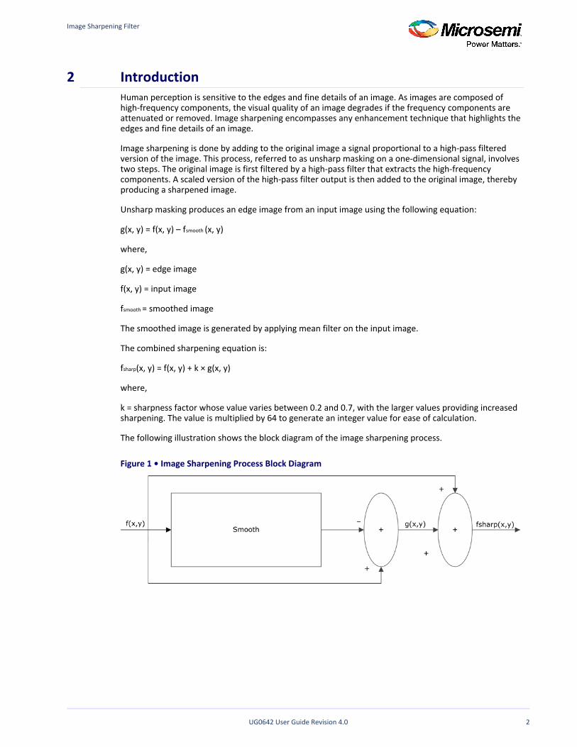
Image Sharpening Filter
UG0642 User Guide Revision 4.0 2
2 IntroductionHuman perception is sensitive to the edges and fine details of an image. As images are composed of high-frequency components, the visual quality of an image degrades if the frequency components are attenuated or removed. Image sharpening encompasses any enhancement technique that highlights the edges and fine details of an image.
Image sharpening is done by adding to the original image a signal proportional to a high-pass filtered version of the image. This process, referred to as unsharp masking on a one-dimensional signal, involves two steps. The original image is first filtered by a high-pass filter that extracts the high-frequency components. A scaled version of the high-pass filter output is then added to the original image, thereby producing a sharpened image.
Unsharp masking produces an edge image from an input image using the following equation:
g(x, y) = f(x, y) – f (x, y)smooth
where,
g(x, y) = edge image
f(x, y) = input image
f = smoothed imagesmooth
The smoothed image is generated by applying mean filter on the input image.
The combined sharpening equation is:
f (x, y) = f(x, y) + k × g(x, y)sharp
where,
k = sharpness factor whose value varies between 0.2 and 0.7, with the larger values providing increased sharpening. The value is multiplied by 64 to generate an integer value for ease of calculation.
The following illustration shows the block diagram of the image sharpening process.
Figure 1 • Image Sharpening Process Block Diagram

Image Sharpening Filter
UG0642 User Guide Revision 4.0 3
3 Hardware ImplementationMicrosemi Image Sharpening Filter IP core—a part of Microsemi’s imaging and video solutions IP suite—contains an unsharp masking algorithm with programmable gain for edge directions.
The Image Sharpening Filter hardware contains four one-line buffers storing one horizontal video line each. The incoming data stream fills these four buffers, one by one. In the design illustrated in this document, the median filter is implemented on a 3 × 3 matrix, so three lines of the video form the 3 × 3 window for the median. When the third buffer contains three pixel values, the read process is initiated.
Median filtering is only applied on channel Y. The Cb and Cr components are passed through the delay registers in order to be synchronized with channel Y. For channel Y, three pixels from each of the three video lines are read into three shift registers that form the 3 × 3 2D array for median calculation. The shift registers are applied as input to the 3 × 3 unsharp masking kernel, and the input is multiplied according to the unsharp kernel matrix shown in the following figure.
Figure 2 • Unsharp Masking Kernel Matrix
The new pixel column is shifted into the shift register, with the oldest data in the register being shifted out. The processed YCbCr value is sent to the sharpening equation to get the pixel sharpened. The sharpened pixels are sent out with a data valid signal. The 3 × 3 window moves from the left to right and from top to bottom for each frame.

Image Sharpening Filter
UG0642 User Guide Revision 4.0 4
The following illustration shows the block diagram of the Image Sharpening Filter hardware.
Figure 3 • Image Sharpening Filter Hardware
3.1 Inputs and OutputsThe following table lists the input and output ports of the Image Sharpening Filter.
Table 1 • Image Sharpening Filter Ports
Signal Name Description Width Description
RESET_n_1 Input Active-low asynchronous reset signal to design.
SYS_CLK_I Input System clock.
Y_in_i Input [(g_DATAWIDTH / 3) –1:0]
Y pixel data input.
Cb_in_i Input [(g_DATAWIDTH / 3) –1:0]
Cb pixel data input.
Cr_in_i Input [(g_DATAWIDTH / 3) –1:0]
Cr pixel data input.
Data_In_Vld_i Input Input data valid signal.
Image Sharpening Filter
UG0642 User Guide Revision 4.0 5
Signal Name Description Width Description
sharpness_K Input 8 bits Sharpness factor. Valid range is from 0.2 to 0.7. The value is multiplied by 64 to generate an integer value for ease of calculation.
Y_Out_o Output [(g_DATAWIDTH / 3) –1:0]
Y pixel data output.
Cb_Out_o Output [(g_DATAWIDTH / 3) – 1:0]
Cb pixel data output.
Cr_Out_o Output [(g_DATAWIDTH / 3) – 1:0]
Cr pixel data output.
data_Vld_out_o Output Output data valid signal.
3.2 Configuration ParametersThe following table lists the configuration parameters for the Image Sharpening Filter design.
Table 2 • Configuration Parameters
Name Description
g_DATAWIDTH Defines Y data bit width
g_X_RES_WIDTH Defines resolution bit width
g_DISPLAY_RESOLUTION Defines the horizontal display resolution
g_VERT_DISPLAY_RESOLUTION Defines the Vertical resolution data width
These are generic parameters that vary based on the application requirements.
3.3 FSM ImplementationDuring the Image Sharpening Filter finite state machine (FSM) implementation, the FSM goes through the following states:
idle: After the module is reset, the FSM goes into idle state and waits for the third pixel of the third line to be read. It then proceeds to check_line_compl.check_line_compl: The FSM waits for the output pixel count to be equal to the display resolution. It then proceeds to last_line_written.last_line_written: The FSM waits for the last input line. If the last line is written, it proceeds to check_frame_compl, else it proceeds to check_input_data.check_input_data: The FSM waits for the fourth pixel of the last line to be written into the line buffer. It then proceeds to check_frame_compl.check_frame_compl: The FSM waits for the output line count to be equal to the vertical resolution width. If the output is the last line, it proceeds to last_line, else it goes to check_line_compl.last_line: The FSM waits for the last output pixel of the last line and then moves back to idle state.

Image Sharpening Filter
UG0642 User Guide Revision 4.0 6
The following illustration shows the FSM implementation for the Image Sharpening Filter.
Figure 4 • Image Sharpening Filter FSM

Image Sharpening Filter
UG0642 User Guide Revision 4.0 7
3.4 Timing DiagramThe following illustration shows the timing diagram of the Image Sharpening Filter.
Figure 5 • Image Sharpening Filter Timing Diagram
3.5 TestbenchTo demonstrate the functionality of the Image Sharpen core, a sample test bench file (
) is available in the Stimulus Hierarchy (View > Windows > Stimulus Image_Sharpen_Filter_tb.vHierarchy), and a sample test bench input image file ( ) is available in the stimulus rgb_in.txtdirectory within the Libero® SoC Files window (View > Windows > Files).
The following table lists the test bench parameters that can be configured according to the application, if necessary.
Table 3 • Test Bench Configuration Parameters
Name Description
CLKPERIOD Clock period
HEIGHT Height of the image
WIDTH Width of the image
WAIT Number of clock cycles of delay between the transmission of one line of the input image and the next
IMAGE_FILE_NAME Input image name
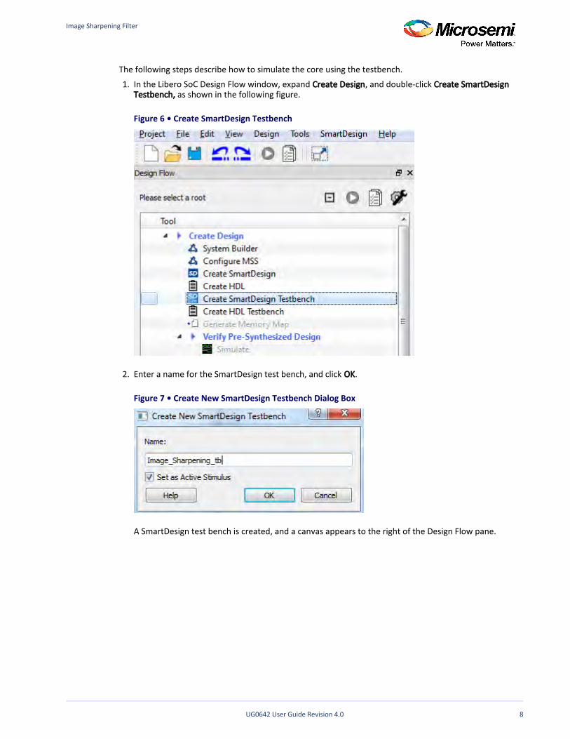
Image Sharpening Filter
UG0642 User Guide Revision 4.0 8
1.
2.
3.
The following steps describe how to simulate the core using the testbench.
In the Libero SoC Design Flow window, expand , and double-click Create Design Create SmartDesign as shown in the following figure.Testbench,
Figure 6 • Create SmartDesign Testbench
Enter a name for the SmartDesign test bench, and click .OK
Figure 7 • Create New SmartDesign Testbench Dialog Box
A SmartDesign test bench is created, and a canvas appears to the right of the Design Flow pane.
In the Libero SoC Catalog (View > Windows > Catalog), expand and drag the Image Solutions-Video,

Image Sharpening Filter
UG0642 User Guide Revision 4.0 9
3.
4.
In the Libero SoC Catalog (View > Windows > Catalog), expand and drag the Image Solutions-Video,Sharpen IP core onto the SmartDesign test bench canvas.
Figure 8 • Image Sharpen Core in Libero SoC Catalog
The core appears on the canvas, as shown in the following figure.
Figure 9 • Image Sharpen Core on SmartDesign Test Bench Canvas
Select all the ports of the core, right-click, and click , as shown in the following Promote to Top Level

Image Sharpening Filter
UG0642 User Guide Revision 4.0 10
4. Select all the ports of the core, right-click, and click , as shown in the following Promote to Top Levelfigure.
Figure 10 • Promote to Top Level Option

Image Sharpening Filter
UG0642 User Guide Revision 4.0 11
4.
5.
6.
The ports are promoted to the top level, as shown in the following figure.
Figure 11 • Image Sharpening Filter Ports Promoted to Top Level
To generate the Image Sharpening Filter SmartDesign component, click the Generate Component icon on the SmartDesign Toolbar, as shown in the following figure.
Figure 12 • Generate Component Icon
A sample test bench input image file is created at: …\Project_name\component\Microsemi\SolutionCore\ImageSharpenFilter\1.0.1\Stimulus
In the Libero SoC Files window, right-click the simulation directory, and click , as shown Import files...

Image Sharpening Filter
UG0642 User Guide Revision 4.0 12
6.
7.
In the Libero SoC Files window, right-click the simulation directory, and click , as shown Import files...in the following figure.
Figure 13 • Import Files Option
Do one of the following:

Image Sharpening Filter
UG0642 User Guide Revision 4.0 13
7.
8.
9.
Do one of the following:
To import the sample test bench input image, browse to the sample test bench input image file, and click , as shown in the following figure.Open
Figure 14 • Input Image File Selection
To import a different image, browse to the folder containing the image file, and click . The Openinput image file appears in the simulation directory, as shown in the following figure.
Figure 15 • Input Image File in Simulation Directory
In the Stimulus Hierarchy, expand , and right-click the Image Sharpening Filter test bench file (Work).Image_Sharpen_Filter_tb.v
Click , then click .Simulate Pre Synth Design Open Interactively

Image Sharpening Filter
UG0642 User Guide Revision 4.0 14
9.
10.
Click , then click .Simulate Pre Synth Design Open Interactively
Figure 16 • Open Interactively Option
The ModelSim tool appears with the test bench file loaded onto it, as shown in the following figure.
Figure 17 • ModelSim Tool with Image Sharpening Filter Test Bench File
If the simulation is interrupted because of the runtime limit in the DO file, use the run -allcommand to complete the simulation.
After the simulation is completed, the test bench output image file (.txt) appears in the simulation folder.

Image Sharpening Filter
UG0642 User Guide Revision 4.0 15
3.6 Simulation ResultsThis section shows an image before and after being processed using the Image Sharpening Filter.
The following figure shows the input image.
Figure 18 • Input Image
The following figure shows the output image.
Figure 19 • Output Image

Image Sharpening Filter
UG0642 User Guide Revision 4.0 16
3.7 Resource UtilizationThe image sharpening filter block is implemented on an M2S150T SmartFusion®2 System-on-Chip (SoC) FPGA in the FC1152 package) and PolarFire FPGA (MPF300TS_ES - 1FCG1152E package).
Table 4 • Resource Utilization
Resource Utilization
DFFs 1272
4-Input LUTs 1270
MACC 1
RAM1Kx18 15
RAM64x18 0

Image Sharpening Filter
UG0642 User Guide Revision 4.0 17
Microsemi Corporate HeadquartersOne Enterprise, Aliso Viejo,CA 92656 USAWithin the USA: +1 (800) 713-4113Outside the USA: +1 (949) 380-6100Fax: +1 (949) 215-4996Email: [email protected]
© 2018 Microsemi Corporation. All rights reserved. Microsemi and the Microsemi logo are trademarks of Microsemi Corporation. All other trademarks and service marks are the property of their respective owners.
Microsemi makes no warranty, representation, or guarantee regarding the information contained herein or the suitability of its products and services for any particular purpose, nor does Microsemi assume any liability whatsoever arising out of the application or use of any product or circuit. The products sold hereunder and any other products sold by Microsemi have been subject to limited testing and should not be used in conjunction with mission-critical equipment or applications. Any performance specifications are believed to be reliable but are not verified, and Buyer must conduct and complete all performance and other testing of the products, alone and together with, or installed in, any end-products. Buyer shall not rely on any data and performance specifications or parameters provided by Microsemi. It is the Buyer's responsibility to independently determine suitability of any products and to test and verify the same. The information provided by Microsemi hereunder is provided "as is, where is" and with all faults, and the entire risk associated with such information is entirely with the Buyer. Microsemi does not grant, explicitly or implicitly, to any party any patent rights, licenses, or any other IP rights, whether with regard to such information itself or anything described by such information. Information provided in this document is proprietary to Microsemi, and Microsemi reserves the right to make any changes to the information in this document or to any products and services at any time without notice.
Microsemi Corporation (Nasdaq: MSCC) offers a comprehensive portfolio of semiconductor and system solutions for aerospace & defense, communications, data center and industrial markets. Products include high-performance and radiation-hardened analog mixed-signal integrated circuits, FPGAs, SoCs and ASICs; power management products; timing and synchronization devices and precise time solutions, setting the world's standard for time; voice processing devices; RF solutions; discrete components; enterprise storage and communication solutions; security technologies and scalable anti-tamper products; Ethernet solutions; Power-over-Ethernet ICs and midspans; as well as custom design capabilities and services. Microsemi is headquartered in Aliso Viejo, California, and has approximately 4,800 employees globally. Learn more at www.microsemi.com.
50200642