Conduction in Semiconductors -Review
26
1 ECE 410, Prof. F. Salem/Prof. A. Mason with updates Lecture Notes 6.1 Conduction in Semiconductors -Review • Intrinsic (undoped) Semiconductors – intrinsic carrier concentration ≡ n i = 1.45x10 10 cm -3 , at room temp. – n = p = n i , in intrinsic (undoped) material •n ≡ number of electrons, p ≡ number of holes – mass-action law, np = n i 2 =1.45E10, applies to undoped and doped material • Extrinsic (doped) Semiconductors – dopants added to modify material/electrical properties P B P B + + + + - - group V element group III element ion electron hole n-type Donor p-type Acceptor ion free carrier free carrier •n-type (n+), add elements with extra an electron –N d ≡ conc. of donor atoms [cm -3 ] –n n = N d , n n ≡ conc. of electrons in n-type material –p n = n i 2 /N d , using mass-action law, –p n ≡ conc. of holes in n-type material –always a lot more n than p in n-type material •p-type = p+, add elements with an extra hole –N a ≡ concentration of acceptor atoms [cm -3 ] –p p = N a , p p ≡ conc. of holes in p-type material –n p = ni 2 /N a , using mass-action law, –n p ≡ conc. of electrons in p-type material –always a lot more p than n in p-type material
Transcript of Conduction in Semiconductors -Review

1
ECE 410, Prof. F. Salem/Prof. A. Mason with updates Lecture Notes 6.1
Conduction in Semiconductors -Review• Intrinsic (undoped) Semiconductors
– intrinsic carrier concentration ≡ ni = 1.45x1010 cm-3, at room temp.– n = p = ni, in intrinsic (undoped) material
• n ≡ number of electrons, p ≡ number of holes– mass-action law, np = ni
2=1.45E10, applies to undoped and doped material
• Extrinsic (doped) Semiconductors– dopants added to modify material/electrical properties
P BP B+ ++
+--
group Velement
group IIIelement
ion
electron hole
n-type Donor p-type Acceptor
ionfreecarrier
freecarrier
•n-type (n+), add elements with extra an electron–Nd ≡ conc. of donor atoms [cm-3]–nn = Nd, nn ≡ conc. of electrons in n-type material–pn = ni
2/Nd, using mass-action law, –pn ≡ conc. of holes in n-type material–always a lot more n than p in n-type material
•p-type = p+, add elements with an extra hole–Na ≡ concentration of acceptor atoms [cm-3]
–pp = Na, pp ≡ conc. of holes in p-type material
–np = ni2/Na, using mass-action law,
–np ≡ conc. of electrons in p-type material
–always a lot more p than n in p-type material

2
ECE 410, Prof. F. Salem/Prof. A. Mason with updates Lecture Notes 6.2
Conduction in Semiconductors• doping provides free charge carriers, alters conductivity • conductivity, σ, in semic. w/ carrier densities n and p
– σ = q(μnn + μpp), q ≡ electron charge, q = 1.6x10⁻¹⁹ [Coulombs]• μ ≡ mobility [cm2/V-sec], μn ≅ 1360, μp ≅ 480 (typical values)
• in n-type region, nn >> pn– σ ≈ qμnnn
• in p-type region, pp >> np
– σ ≈ qμpnp
• resistivity, ρ = 1/σ• resistance of an n+ or p+ region
– R = ρ l , A = wt
• drift current (flow of charge carriers in presence of an electric field, Ex)– n/p drift current density: Jxn = σn Ex = qμnnnEx, Jxp = σp Ex = qμpppEx
– total drift current density in x direction Jx = q(μnn + μpp) Ex = σ Ex
mobility = average velocity per unit electric field
μn > μpelectrons more mobile than holes
⇒conductivity of n+ > p+
l
t
wA

3
ECE 410, Prof. F. Salem/Prof. A. Mason with updates Lecture Notes 6.3
pn Junctions: Intro• What is a pn Junction?
– interface of p-type andn-type semiconductor
– junction of two materials forms a diode
• In the Beginning…– ionization of dopants
at material interface
• Diffusion -movement of charge to regions of lower concentration– free carriers diffuse out– leave behind immobile ions– region become depleted of
free carriers– ions establish an electric field
• acts against diffusion
donor ion and electron free carrier
acceptor ion and hole free carrier
p-type
hole diffusionhole current
electron diffusionelectron current
N acceptors/cmA
3
N donors/cmD
3
n-type
-+
-+-+
-+-+
-+
-+-+
+-
+-+-+-+-+-+-
+-+-+-+-
Edepletion region
immobile acceptor ions(negative-charge)
immobile donor ions(positive-charge)
electric field
xp
W
xn
----
----
+++
+++
++
p-type
N acceptors/cmA
3
N donors/cmD
3
n-type
p-type Si wafer
pn diodejunction
depletion regionboundaries
dielectricinsulator(oxide)
contactto p-side
contactto n-side
p+ n+
n “well”
p-type n-type

4
ECE 410, Prof. F. Salem/Prof. A. Mason with updates Lecture Notes 6.4
pn Junctions: Equilibrium Conditions• Depletion Region
– area at pn interface void of free charges
– charge neutrality• must have equal charge on both sides• q A xp NA = q A xn ND , A=junction area; xp, xn depth into p/n side• ⇒ xp NA = xn ND• depletion region will extend further into the more lightly doped side
of the junction
• Built-in Potential– diffusion of carriers leaves behind immobile charged ions– ions create an electric field which generates a built-in potential
• where VT = kT/q = 26mV at room temperature
Edepletion region
immobile acceptor ions(negative-charge)
immobile donor ions(positive-charge)
electric field
xp
W
xn
----
----
+++
+++
++
p-type
N acceptors/cmA
3
N donors/cmD
3
n-type
NA ND
⎟⎟⎠
⎞⎜⎜⎝
⎛=Ψ 20 ln
i
DAT n
NNV

5
ECE 410, Prof. F. Salem/Prof. A. Mason with updates Lecture Notes 6.5
pn Junctions: Depletion Width• Depletion Width
use Poisson’s equation & charge neutrality– W = xp + xn
• where VR is applied reverse bias
• One-sided Step Junction– if NA>>ND (p+n diode)
• most of junction on n-side
– if ND>>NA (n+p diode)• most of junction on p-side
Edepletion region
immobile acceptor ions(negative-charge)
immobile donor ions(positive-charge)
electric field
xp
W
xn
----
----
+++
+++
++
p-type
N acceptors/cmA
3
N donors/cmD
3
n-type
NA ND
⎟⎟⎠
⎞⎜⎜⎝
⎛=Ψ 20 ln
i
DAT n
NNV
( )( )
21
02⎥⎦
⎤⎢⎣
⎡+
+Ψ=
ADA
DRp NNqN
NVx
ε ( )( )
21
02⎥⎦
⎤⎢⎣
⎡+
+Ψ=
ADD
ARn NNqN
NVx
ε
( ) 21
02⎥⎦
⎤⎢⎣
⎡ ++Ψ=
AD
ADR
NNNN
qV
Wε
( ) 21
02⎥⎦
⎤⎢⎣
⎡ +Ψ=≅
A
Rp qN
VxW
ε
( ) 21
02⎥⎦
⎤⎢⎣
⎡ +Ψ=≅
D
Rn qN
VxW
ε
ε is the permittivity of Siε = 1.04x10⁻¹² F/cmε = KSε0, where ε0 = 8.85x10⁻¹⁴ F/cmand KS = 11.8 is the relative permittivity of silicon

6
ECE 410, Prof. F. Salem/Prof. A. Mason with updates Lecture Notes 6.6
pn Junctions - Depletion Capacitance• Free carriers are separated by the depletion layer• Separation of charge creates junction capacitance
– Cj = εA/d ⇒ (d = depletion width, W)
– A is complex to calculate in semiconductor diodes• consists of both bottom of the well and side-wall areas
– Cj is a strong function of biasing• must be re-calculated if
bias conditions change– CMOS doping is not linear/constant
• graded junction approximation
• Junction Breakdown– if reverse bias is too high (typically > 30V) can get strong reverse current flow
( ) ⎟⎟
⎠
⎞
⎜⎜
⎝
⎛
+Ψ⎥⎦
⎤⎢⎣
⎡+
=RDA
DAj
VNNNNq
AC0
21
12
ε ε is the permittivity of Siε = 11.8 ε0 = 1.04x10⁻¹² F/cmVR = applied reverse bias
⎟⎟⎟⎟⎟
⎠
⎞
⎜⎜⎜⎜⎜
⎝
⎛
Ψ+
=
01 R
joj
V
CC
( )2
1
02 ⎥⎦
⎤⎢⎣
⎡+Ψ
=DA
DAjo NN
NNqAC ε
⎟⎟⎟⎟⎟
⎠
⎞
⎜⎜⎜⎜⎜
⎝
⎛
Ψ+
=
30
1 R
joj
V
CC

7
ECE 410, Prof. F. Salem/Prof. A. Mason with updates Lecture Notes 6.7
• Forward Bias; VD > Ψ0– acts against built-in potential– depletion width reduced– diffusion currents increase with VD
• minority carrier diffusion
• Reverse Bias; VR = -VD > 0– acts to support built-in potential– depletion width increased– electric field increased– small drift current flows
• considered leakage• small until VR is too high and breakdown occurs
Diode Biasing and Current Flow+ V -
D
VD
Vf
+ V -D
ID
ID
ID
p n
( )1−= TD VVSD eII ⎟⎟
⎠
⎞⎜⎜⎝
⎛+∝
ADS NN
AI 11

8
ECE 410, Prof. F. Salem/Prof. A. Mason with updates Lecture Notes 6.8
MOSFET Capacitor• MOSFETs move charge from drain to source underneath the gate,
if a conductive channel exists under the gate• Understanding how and why the conductive channel is produced is
important• MOSFET capacitor models the gate/oxide/substrate region
– source and drain are ignored– substrate changes with applied gate voltage
• Consider an nMOS device– Accumulation, VG < 0, (-)ve charge on gate
• induces (+)ve charge in substrate• (+)ve charge accumulate from substrate p+
– Depletion, VG > 0 but small• creates depletion region in subst.• (-) charge but no free carriers
– Inversion, VG > 0 but larger• further depletion requires high energy• (-) charge pulled from Ground• e- free carriers in channel
Si substrate = bulk
gate oxide
G
GS D
B
B
gate
channel =
p-type Si substrate
depletion layer depletion layer
Accumulation Depletion Inversion
p-type Si substrate p-type Si substrate
V < 0G
V > 0G
V >> 0G
B B B
+ + + + + + ++ + + + + + + + + + + + + + + + + + + + + + + + + + + +- - - - - - -- - - - - - - - - - - - - -- - - - - - - - - -

9
ECE 410, Prof. F. Salem/Prof. A. Mason with updates Lecture Notes 6.9
Capacitance in MOSFET Capacitor• In Accumulation
– Gate capacitance = Oxide capacitance– Cox = εox/tox [F/cm2]
• In Depletion– Gate capacitance has 2 components– 1) oxide capacitance– 2) depletion capacitance of the substrate depletion region
• Cdep = εsi/xd, xd = depth of depletion region into substrate– Cgate = Cox || Cdep = Cox Cdep / (Cox+Cdep) < Cox
• In Inversion– free carries at the surface– Cgate = Cox
Cgate
VG
Cox
inversiondepletion
accumulation
Cox
Cdep

10
ECE 410, Prof. F. Salem/Prof. A. Mason with updates Lecture Notes 6.10
Inversion Operation• MOSFET “off” unless in inversion
– look more deeply at inversion operation• Define some stuff
– Qs = total charge in substrate– VG = applied gate voltage– Vox = voltage drop across oxide– φs = potential at silicon/oxide interface (relative to substrate-ground)
– Qs = - Cox VG
– VG = Vox + φs
• During Inversion (for nMOS)– VG > 0 applied to gate– Vox drops across oxide (assume linear)– φs drops across the silicon substrate, most near the surface

11
ECE 410, Prof. F. Salem/Prof. A. Mason with updates Lecture Notes 6.11
Surface Charge• QB = bulk charge, ion charge in depletion region under
the gate– QB = - q NA xd, xd = depletion depth– QB = - (2q εSi NA φs)1/2 = f(VG)– charge per unit area
• Qe = charge due to free electrons at substrate surface• Qs = QB + Qe < 0 (negative charge for nMOS)
( ) 21
02⎥⎦
⎤⎢⎣
⎡ +Ψ=≅
D
Rn qN
VxW
εrecall from pn junction,when ND>>NA
depletionregion QB, bulk
charge
electronlayer, Qe
A

12
ECE 410, Prof. F. Salem/Prof. A. Mason with updates Lecture Notes 6.12
Surface Charge vs. Gate Voltage• Surface Charge vs. Gate Voltage
– VG < Vtn, substrate charge is all bulk charge, Qs = QB
– VG = Vtn, depletion region stops growing• xd at max., further increase of VG will NOT increase xd• QB at max.
– VG > Vtn, substrate charge has both components, Qs = QB + Qe• since QB is maxed, further increases in VG must increase Qe• increasing Qe give more free carriers thus less resistance
• Threshold Voltage– Vtn defined as gate voltage where Qe starts to form– Qe = -Cox (VG-Vtn)– Vtn is gate voltage required to
• overcome material difference between silicon and oxide• establish depletion region in channel to max value/size

13
ECE 410, Prof. F. Salem/Prof. A. Mason with updates Lecture Notes 6.13
Overview of MOSFET Current• Gate current
– gate is essentially a capacitor ⇒ no current through gate– gate is a control node
• VG < Vtn, device is off• VG > Vtn, device is on and performance is a function of VGS and VDS
• Drain Current (current from drain to source), ID– Source = source/supply of electrons (nMOS) or holes (pMOS)– Drain = drain/sink of electrons (nMOS) or holes (pMOS)– VDS establishes an E-field across the channel (horizontally)
• free charge in an E-field will create a drain-source current• is ID drift or diffusion current?
• MOSFET I-V Characteristics
nMOS
drain @ (+)ve potential
Electron FlowCurrent Flow
source @ ground
Charge FlowCurrent Flow
↑ VGS
VDS = VGS - Vtn

14
ECE 410, Prof. F. Salem/Prof. A. Mason with updates Lecture Notes 6.14
nMOS Current vs.Voltage• Cutoff Region
– VGS < Vtn⇒ID = 0 (Not quiet--there is leakage “subthreshold current”)
• Linear Region– VGS > Vth, VDS > 0 but very small
• Qe = -Cox (VGS-Vtn)• ID = μn Qe (W/L) VDS
⇒ ID = μnCox (W/L) (VGS-Vtn) VDS
• Triode Region– VGS > Vth, 0 < VDS < VGS-Vth
• surface potential, φs , at drain now f(VGS-VDS=VGD) ⇒ less charge near drain • assume channel charge varies linearly from drain to source
– at source: Qe = -Cox (VGS-Vtn), at drain: Qe = 0⇒
∫=DV
ID yVyQI0
)()( δα
[ ]2)(22 DSDStGS
OXnD VVVV
LWC
I −−=μ
General Integral for expressing ID• channel charge = f(y)• channel voltage = f(y)• y is direction from drain to source
↑ VGS
VDS = VGS - Vtn

15
ECE 410, Prof. F. Salem/Prof. A. Mason with updates Lecture Notes 6.15
nMOS Current vs.Voltage• Saturation Region (Active Region)
– VGS > Vtn, VDS > VGS-Vtn• surface potential at drain, φsd = VGS-Vtn-VDS• when VDS = VGS-Vtn, φsd = 0 ⇒ channel not inverted at the drain
– channel is said to be pinched off• during pinch off, further increase in VDS will not increase ID
– define saturation voltage, Vsat, when VDS = VGS-Vtn• current is saturated, no longer increases• substitute Vsat=VGS-Vtn for VDS into triode equation
⇒2)(
2 tGSOXn
D VVLWC
I −=μ
square lawequation
[ ]2)(22 DSDStGS
OXnD VVVV
LWC
I −−=μ

16
ECE 410, Prof. F. Salem/Prof. A. Mason with updates Lecture Notes 6.16
Other Stuff• Transconductance
– process transconductance, k’ = μn Cox• constant for a given fabrication process
– device transconductance, βn= k’ W/L• Surface Mobility
– mobility at the surface is lower than mobility deep inside silicon– for current, ID, calculation, typical μn = 500-580 cm2/V-sec
• Effective Channel Length– effective channel length reduced by
• lateral diffusion under the gate• depletion spreading from drain-substrate junction
dD XLdrawnLLeff −−= 2)(( )( )
⎟⎟⎠
⎞⎜⎜⎝
⎛ −−=
A
tGDsd qN
VVVX
ε2
GS
L (drawn)
Leff
LDx
d~x
d
D

17
ECE 410, Prof. F. Salem/Prof. A. Mason with updates Lecture Notes 6.17
Second Order Effects• Channel Length Modulation
– Square Law Equation predicts ID is constant with VDS– However, ID actually increases slightly with VDS
• due to effective channel getting shorter as VDS increases• effect called channel length modulation
– Channel Length Modulation factor, λ• models change in channel length with VDS
– Corrected ID equation
• Veff = VGS - Vtn• Body Effect
– so far we have assumed that substrate and source are grounded– if source not at ground, source-to-bulk voltage exists, VSB > 0– VSB > 0 will increase the threshold voltage, Vtn = f(VSB)– called Body Effect, or Body-Bias Effect
( ))(1)(2
2effDStGS
OXnD VVVV
LWCI −+−= λμ

18
ECE 410, Prof. F. Salem/Prof. A. Mason with updates Lecture Notes 6.18
pMOS Equations• analysis of nMOS applies to pMOS with
following modifications– physical
• change all n-type regions to p-type• change all p-type regions to n-type
– substrate is n-type (pWell)• channel charge is positive (holes) and (+)ve charged ions
– equations• change VGS to VSG (VSG typically = VDD - VG)• change VDS to VSD (VSD typically = VDD - VD)• change Vtn to |Vtp|
– pMOS threshold is negative, nearly same magnitude as nMOS– other factors
• lower surface mobility, typical value, μp = 220 cm2/V-sec• body effect, change VSB to VBS

19
ECE 410, Prof. F. Salem/Prof. A. Mason with updates Lecture Notes 6.19
MOSFET RC Model• Modeling MOSFET resistance and capacitance is very
important for transient characteristics of the device• RC Model
• Drain-Source (channel) Resistance, Rn– Rn = VDS / ID
• function of bias voltages– point (a), linear region
• Rn = 1/[βn(VGS-Vtn)]– point (b), triode region
• Rn = 2/{βn[2(VGS-Vtn)-VDS]}– point (c), saturation region
• Rn = 2VDS / [βn (VGS-Vtn)2]– general model equation
• Rn = 1/[βn(VDD-Vtn)]

20
ECE 410, Prof. F. Salem/Prof. A. Mason with updates Lecture Notes 6.20
MOSFET Capacitances -Preview• Need to find CS and CD
• MOSFET Small Signal model– Model Capacitances
• Cgs• Cgd• Cgb• Cdb• Csb• no Csd!
• MOSFET PhysicalCapacitances– layer overlap– pn junction
+v-
gs
vsis
vg vd
idg vmb sbg vm gs
roCgs
Cgb
Csb
Cdb
CgdGate Drain
Source
Body (Bulk)
21
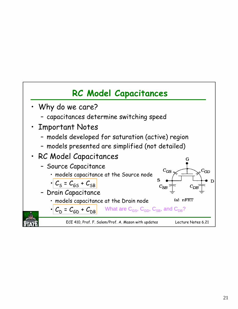
ECE 410, Prof. F. Salem/Prof. A. Mason with updates Lecture Notes 6.21
RC Model Capacitances• Why do we care?
– capacitances determine switching speed• Important Notes
– models developed for saturation (active) region– models presented are simplified (not detailed)
• RC Model Capacitances– Source Capacitance
• models capacitance at the Source node• CS = CGS + CSB
– Drain Capacitance• models capacitance at the Drain node• CD = CGD + CDB What are CGS, CGD, CSB, and CDB?

22
ECE 410, Prof. F. Salem/Prof. A. Mason with updates Lecture Notes 6.22
MOSFET Parasitic Capacitances• Gate Capacitance
– models capacitance due to overlap of Gate and Channel• CG = Cox W L
– estimate that CG is split 50/50 between Source and Drain• CGS = ½ CG
• CGD = ½ CG
– assume Gate-Bulk capacitance is negligible• models overlap of gate with substrate outside the active tx area• CGB = 0
• Bulk Capacitance– CSB (Source-Bulk) and CDB (Drain-Bulk)
• pn junction capacitances
⎟⎟⎠
⎞⎜⎜⎝
⎛
Ψ+=
0
1 Rjoj
VCC ( )2
1
02 ⎥⎦
⎤⎢⎣
⎡+Ψ
=DA
DAjo NN
NNqAC ε
What are VR, Ψ0, NA, and ND?
NA
ND

23
ECE 410, Prof. F. Salem/Prof. A. Mason with updates Lecture Notes 6.23
MOSFET Junction Capacitances• Capacitance/area for pn Junction
• S/D Junction Capacitance– zero-bias capacitance
• highest value when VR = 0, assume this for worst-case estimate• Cj = Cjo
– CS/Dj = Cjo AS/D, AS/D = area of Source/Drain
• what is AS/D?• complex 3-dimensional geometry
– bottom region and sidewall regions
– CS/Dj = Cbot + Csw• bottom and side wall capacitances
21
02 ⎥⎦
⎤⎢⎣
⎡Ψ
= Ajo
NqC ε
assuming ND (n+ S/D) >> NA (p subst.)
jm
Rjoj
VCC ⎟⎟⎠
⎞⎜⎜⎝
⎛Ψ
+=0
1
mj = grading coefficient (typically 1/3)
⎟⎟⎠
⎞⎜⎜⎝
⎛=Ψ 20 ln
i
DAT n
NNV

24
ECE 410, Prof. F. Salem/Prof. A. Mason with updates Lecture Notes 6.24
Junction Capacitance• Bottom Capacitance
– Cbot = Cj Abot• Abot = X W
• Sidewall Capacitance– Csw = Cjsw Psw
• Cjsw = Cj xj [F/cm]– xj = junction depth
• Psw = sidewall perimeter – Psw = 2 (W + X)
• Accounting for Gate Undercut– junction actually under gate also due to lateral diffusion– X ⇒ X + LD (replace X with X + LD)
• Total Junction Cap– CS/Dj = Cbot + Csw = Cj Abot + Cjsw Psw = CS/Dj
xj

25
ECE 410, Prof. F. Salem/Prof. A. Mason with updates Lecture Notes 6.25
MOSFET Bulk Capacitances• General Junction Capacitance
– CS/Dj = Cbot + Csw• CSB (Source-Bulk)
– CSB = Cj ASbot + Cjsw PSsw• CDB (Drain-Bulk)
– CDB = Cj ADbot + Cjsw PDsw
• RC Model Capacitances– Source Capacitance
• CS = CGS + CSB– Drain Capacitance
• CD = CGD + CDB
+v-
gs
vsis
vg vd
idg vmb sbg vm gs
roCgs
Cgb
Csb
Cdb
CgdGate Drain
Source
Body (Bulk)

26
ECE 410, Prof. F. Salem/Prof. A. Mason with updates Lecture Notes 6.26
Junction Areas• Note: calculations assume following design rules
– poly size, L = 2λ– poly space to contact, 2λ– contact size, 2λ– active overlap of contact, 1λ
• Non-shared Junction with Contact– Area: X1 W = (5)(4) = 20λ2
– Perimeter: 2(X1 + W) = 18λ• Shared Junction without Contact
– Area: X2 W = (2)(4)λ2 = 8λ2
– Perimeter: 2(X2 + W) = 12λ• much smaller!
• Shared Junction with Contact– Area: X3 W = (6)(4)λ2 = 24λ2
– Perimeter: 2(X3 + W) = 20λ• largest area!
W = 4λX1 = 5λ, X2= 2λ, X3 = 6λ⇒
X1
X2
X3