Concentrating light in Cu(In,Ga)Se2 solar cells a,b a a,b ... · Concentrating light in...
7
*[email protected]; phone +49(0)30/8062-43243; www.helmholtz-berlin.de Concentrating light in Cu(In,Ga)Se2 solar cells M. Schmid* a,b , G. Yin a , M. Song a,b , S. Duan a , B. Heidmann a,b , D. Sancho-Martinez a , S. Kämmer a,b , T. Köhler a , P. Manley a , M.Ch. Lux-Steiner b,c a Nanooptische Konzepte für die PV, Helmholtz-Zentrum Berlin, Hahn-Meitner-Platz 1, 14109 Berlin, Germany; b Department of Physics, Freie Universität Berlin, Arnimallee 14, 14195 Berlin, Germany; c Helmholtz-Zentrum Berlin, Hahn-Meitner-Platz 1, 14109 Berlin, Germany; ABSTRACT Light concentration has proven beneficial for solar cells, most notably for highly efficient but expensive absorber materials using high concentrations and large scale optics. Here we investigate light concentration for cost efficient thin- film solar cells which show nano- or microtextured absorbers. Our absorber material of choice is Cu(In,Ga)Se2 (CIGSe) which has a proven stabilized record efficiency of 22.6% and which - despite being a polycrystalline thin-film material - is very tolerant to environmental influences. Taking a nanoscale approach, we concentrate light in the CIGSe absorber layer by integrating photonic nanostructures made from dielectric materials. The dielectric nanostructures give rise to resonant modes and field localization in their vicinity. Thus when inserted inside or adjacent to the absorber layer, absorption and efficiency enhancement are observed. In contrast to this internal absorption enhancement, external enhancement is exploited in the microscale approach: mm-sized lenses can be used to concentrate light onto CIGSe solar cells with lateral dimensions reduced down to the micrometer range. These micro solar cells come with the benefit of improved heat dissipation compared to the large scale concentrators and promise compact high efficiency devices. Both approaches of light concentration allow for reduction in material consumption by restricting the absorber dimension either vertically (ultra-thin absorbers for dielectric nanostructures) or horizontally (micro absorbers for concentrating lenses) and have significant potential for efficiency enhancement. Keywords: chalcopyrite solar cells, CIGSe, ultra-thin absorber, nanoparticles, photonics, light concentration, micro absorber, optical modeling 1. INTRODUCTION Thin-film solar cells based on Cu(In,Ga)Se2 (CIGSe) are experiencing an exciting continuous raise in record efficiencies, the current record being 22.6% [1]. This development can be expected to further increase the share of CIGSe solar cells in the photovoltaic market. When envisaging production on the Terrawatt-scale, however, the price and supply risk of the contained elements indium and gallium may become a limiting factor [2]. Saving absorber material whilst maintaining or even increasing the efficiency therefore is a central goal to further foster CIGSe competitiveness. Aside from the proven high record efficiencies, CIGSe solar cells offer the additional benefit of being very tolerant against environmental factors such as shading or even cosmic radiation [3]. This ability makes them a natural fit for novel concepts which offer material saving and efficiency enhancement, but at the same time perturb the standard growth processes or involve non-uniform illumination conditions. For material saving purpose, the absorber dimensions can be reduced in two ways: either vertically by decreasing the absorber thickness from the standard 2-3 μm to below 500 nm, or horizontally depositing spaced out periodically placed absorbers of about 100-400 μm diameter. Both cases will initially lead to a loss of incident light due to incomplete absorption in the ultra-thin CIGSe or due to light passing in between the locally restricted micro absorbers, respectively. The initial loss of incident sun light needs to be tackled by sophisticated concepts for light localization inside the reduced absorber volume. On the nanoscale, plasmonic and photonic nanostructures are a promising approach to trap light in ultra-thin layers by near-field enhancement, large-angle scattering and coupling into waveguide modes [4]. Absorption enhancement by nanostructures has been proven for various types of photovoltaic devices like silicon or organic solar cells [5]. Recently, we also have delivered the experimental proof of absorption enhancement by dielectric nanostructures in ultra-thin CIGSe solar cells [6, 7]. Based on this first verification, further development became attractive and offers highly promising improvement. For the microscaled approach, light concentration onto the local absorbers occurs due to micro lenses which collect the incident
Transcript of Concentrating light in Cu(In,Ga)Se2 solar cells a,b a a,b ... · Concentrating light in...

*[email protected]; phone +49(0)30/8062-43243; www.helmholtz-berlin.de
Concentrating light in Cu(In,Ga)Se2 solar cells M. Schmid*a,b, G. Yina, M. Songa,b, S. Duana, B. Heidmanna,b, D. Sancho-Martineza, S. Kämmera,b,
T. Köhlera, P. Manleya, M.Ch. Lux-Steinerb,c
aNanooptische Konzepte für die PV, Helmholtz-Zentrum Berlin, Hahn-Meitner-Platz 1, 14109 Berlin, Germany; bDepartment of Physics, Freie Universität Berlin, Arnimallee 14, 14195 Berlin,
Germany; cHelmholtz-Zentrum Berlin, Hahn-Meitner-Platz 1, 14109 Berlin, Germany;
ABSTRACT
Light concentration has proven beneficial for solar cells, most notably for highly efficient but expensive absorber materials using high concentrations and large scale optics. Here we investigate light concentration for cost efficient thin-film solar cells which show nano- or microtextured absorbers. Our absorber material of choice is Cu(In,Ga)Se2 (CIGSe) which has a proven stabilized record efficiency of 22.6% and which - despite being a polycrystalline thin-film material - is very tolerant to environmental influences. Taking a nanoscale approach, we concentrate light in the CIGSe absorber layer by integrating photonic nanostructures made from dielectric materials. The dielectric nanostructures give rise to resonant modes and field localization in their vicinity. Thus when inserted inside or adjacent to the absorber layer, absorption and efficiency enhancement are observed. In contrast to this internal absorption enhancement, external enhancement is exploited in the microscale approach: mm-sized lenses can be used to concentrate light onto CIGSe solar cells with lateral dimensions reduced down to the micrometer range. These micro solar cells come with the benefit of improved heat dissipation compared to the large scale concentrators and promise compact high efficiency devices. Both approaches of light concentration allow for reduction in material consumption by restricting the absorber dimension either vertically (ultra-thin absorbers for dielectric nanostructures) or horizontally (micro absorbers for concentrating lenses) and have significant potential for efficiency enhancement. Keywords: chalcopyrite solar cells, CIGSe, ultra-thin absorber, nanoparticles, photonics, light concentration, micro absorber, optical modeling
1. INTRODUCTION
Thin-film solar cells based on Cu(In,Ga)Se2 (CIGSe) are experiencing an exciting continuous raise in record efficiencies, the current record being 22.6% [1]. This development can be expected to further increase the share of CIGSe solar cells in the photovoltaic market. When envisaging production on the Terrawatt-scale, however, the price and supply risk of the contained elements indium and gallium may become a limiting factor [2]. Saving absorber material whilst maintaining or even increasing the efficiency therefore is a central goal to further foster CIGSe competitiveness.
Aside from the proven high record efficiencies, CIGSe solar cells offer the additional benefit of being very tolerant against environmental factors such as shading or even cosmic radiation [3]. This ability makes them a natural fit for novel concepts which offer material saving and efficiency enhancement, but at the same time perturb the standard growth processes or involve non-uniform illumination conditions. For material saving purpose, the absorber dimensions can be reduced in two ways: either vertically by decreasing the absorber thickness from the standard 2-3 µm to below 500 nm, or horizontally depositing spaced out periodically placed absorbers of about 100-400 µm diameter. Both cases will initially lead to a loss of incident light due to incomplete absorption in the ultra-thin CIGSe or due to light passing in between the locally restricted micro absorbers, respectively. The initial loss of incident sun light needs to be tackled by sophisticated concepts for light localization inside the reduced absorber volume. On the nanoscale, plasmonic and photonic nanostructures are a promising approach to trap light in ultra-thin layers by near-field enhancement, large-angle scattering and coupling into waveguide modes [4]. Absorption enhancement by nanostructures has been proven for various types of photovoltaic devices like silicon or organic solar cells [5]. Recently, we also have delivered the experimental proof of absorption enhancement by dielectric nanostructures in ultra-thin CIGSe solar cells [6, 7]. Based on this first verification, further development became attractive and offers highly promising improvement. For the microscaled approach, light concentration onto the local absorbers occurs due to micro lenses which collect the incident

light and focus it onto the small absorbers. Micro concentrator solar cells have equally been demonstrated in the field of silicon photovoltaics [8], but first investigations of the concept also exist in the area of CIGSe [9, 10]. In this paper we give our latest results for the development of absorption enhancement in ultra-thin CIGSe solar cells and light concentration onto micrometer-sized solar cells and highlight both achievements and future challenges. The two concepts of nano- and microscaled light concentration in CIGSe solar cells which we will discuss in the following are depicted in Fig. 1.
Figure 1. Concepts for material saving and efficiency enhancement in CIGSe solar cells: a) ultra-thin solar cell with integrated nanostructures for localizing light inside the absorber material, b) micrometer-sized solar cells under concentrated illumination due to the application of micro lenses.
2. ABSORPTION ENHANCEMENT IN ULTRA-THIN SOLAR CELLS
In standard CIGSe solar cells the absorber thickness is chosen as 2-3 µm to assure high material quality and complete absorption. Despite this, 1 µm thickness is sufficient, in principle, for complete absorption of photons with energies larger than the band gap. The minimum value of 1000 nm absorber thickness above which a high performance of CIGSe solar cells can be assured is a result of optical simulations as well as of experimental investigations [11]. Below 1000 nm thickness, the absorption starts to drop significantly, especially in the long wavelength region, as can also be seen from Fig. 2a. The measured external quantum efficiency (EQE) of CIGSe solar cells with an absorber thicknesses of 240 nm, 440 nm and 670 nm is depicted here, clearly revealing losses close to the band gap which extend more and more towards shorter wavelengths as the absorber thickness decreases. Theoretically, a drop in short circuit current density jSC of approx. 7 mA/cm2 would be expected, experimentally we find an even greater loss of 14 mA/cm2. This is a clear indication that the ultra-thin absorbers not only suffer from reduced absorption, but also electrical properties become deteriorated which is confirmed by a drop in open circuit voltage VOC and fill factor. As the absorber thickness is decreased, on the one hand reduced bulk recombination and improved carrier collection can be expected. But once the back contact is within the diffusion length of the photo-generated majority carriers, interface recombination in particular at the back contact can become dominant. The scanning electron microscope (SEM) cross sections in Fig. 2b show that good material quality with large grains can still be achieved for the ultra-thin devices. Nevertheless, the growth process needs to be adapted for ultra-thin absorbers and optimized as a function of thickness. Based on a three-stage process optimized for 460 nm absorber thickness with a high back Ga gradient for reducing the back recombination we could reach at best an efficiency of 11.3%.
Figure 2. a) External quantum efficiency of thin-film CIGSe solar cells with an absorber thickness of 240 nm, 440 nm and 670 nm, b) cross sectional SEM images of the solar cells with various absorbers thicknesses.

The drop in EQE, and hence loss in conversion efficiency of incident photons to extractable current, places at once the dual demands of enhanced absorption and reduced recombination onto the device design. Plasmonic and photonic nanostructures have proven to be effective means for localization of light in ultra-thin films. The major effects that can be exploited are: scattering of incident light preferentially towards the absorber layer (in the case of plasmonic nanoparticles and a high refractive index absorber), scattering towards large angles and hence enhancement of path length and light trapping in case of total reflection (also mostly for plasmonic nanoparticles), enhancement of electromagnetic field in the direct vicinity of the nanoparticles (near-field enhancement of both plasmonic and photonic nanoparticles), creation of nanojets with high field intensities (by dielectric nano-/microparticles), coupling of light via whispering gallery modes (by dielectric nano-/microparticles) and excitation of waveguide modes redirecting light to propagate inside the absorber layer (by regularly arranged nanoparticles). There are numerous examples for these different effects and in [12] we provide a detailed investigation of various configurations of metallic and dielectric nanostructures in ultra-thin CIGSe solar cells and their potential for absorption enhancement. As already shown in [13], dielectric nanostructures are a highly promising alternative to metallic nanoparticles from an optical point of view and in addition they provide thermally and chemically stable structures suitable to be deposited prior to a high temperature absorber growth process. The integration of nanostructures at the rear interface has proven most effective for CIGSe solar cells since a direct contact to the absorber layer can be established and any influence on the pn-junction avoided.
In Fig. 3 we show results for the absorption of CIGSe solar cells with an absorber thickness of 400 nm and nanostructures integrated at the CIGSe/Mo interface as simulated using the finite element method (JCMsuite). Two configurations were investigated: hemispherical SiO2 nanoparticles with a radius of 275 nm and an inter-particle spacing of 75 nm in a 2D hexagonal arrangement as well as the negative of these structures corresponding to a network of SiO2 obtained by filling the gaps between (inverted hemi-) spheres. The structures are depicted in Fig. 3a where the shape of the SiO2 nanostructures and their integration into the absorber layer as well as the other layers of the CIGSe solar cell can be seen. From the absorption of CIGSe given in Fig. 3b we can observe a significant increase for wavelengths above 700 nm for both cases of nanostructures as compared to the flat reference. The increase in absorption mainly correlates with a reduction of parasitic absorption in Mo, which is most pronounced for the case of SiO2 nanoparticles. Fig. 3c finally depicts the electric field distributions at the major resonances (1070 and 1090 nm wavelength, respectively). The near-field pictures reveal, that the high electric field intensity is localized in the middle of the absorber layer in the case of nanoparticles and thereby avoids being absorbed in the Mo. For the network, however, the CIGSe nanoparticles
Figure 3. Simulation of CIGSe solar cells with integrated SiO2 hemispherical nanoparticles (top row) and SiO2 network (bottom row): a) schematic solar cell structure, b) calculated absorption of CIGSe and Mo back contact as compared to the flat reference, c) electric near-field distribution at the major resonance.

emerging within the SiO2 structure act as cavities localizing the field and giving rise to a high field intensity close to the Mo interface. The dielectric network furthermore creates high intensities in the front contact layers (CdS, ZnO, ZnO:Al) resulting in parasitic absorption. Thus despite both SiO2 structures leading to a significant concentration of electromagnetic field inside the absorber layer, the nanoparticles outperform the network in terms of theoretical absorption enhancement.
In the experiment, however, where not only optical but also electrical influences determine the final performance, the dielectric network turns out highly effective. Fig. 4a shows an SEM cross section of the experimental realization of integrating a SiO2 network at the Mo/CIGSe interface. The network was obtained via a mask of PS spheres with a diameter of 909 nm, which initially formed a closely packed monolayer and were then reduced to 640 nm in diameter by plasma etching. SiO2 was subsequently deposited onto that mask prior to its removal resulting in the visible free standing network in the front part of the SEM picture. For details of the preparation see also [12]. The CIGSe absorber and front layers conformally overgrow the network leading to point contacts with the Mo, which is the added electrical benefit of integrating these optically active dielectric nanostructures. The combined optical and electrical benefit of the network can be deduced from the solar cell parameters given as inset in the EQE measurements of Fig. 4b. The broadband absorption enhancement visible from the EQE reflects an increase in jSC by almost 4 mA/cm2 related to the optical improvement. In addition, an increase in VOC which is significantly larger than it could be expected from the jSC increase is observed and amounts to 50 mV. The origin can be attributed to the SiO2 network leading to point contacts at the rear interface, thus reducing back contact recombination and improving the carrier collection. The electrical benefits of the network hence add to the optical effects of localizing electric field intensity inside the absorber as expected from the optical simulations shown in Fig. 3c. An overall increase in efficiency by 29% relative could be achieved.
Figure 4. a) SEM cross-section of an ultra-thin CIGSe solar cell on top of a SiO2 network, b) corresponding EQE as compared to planar reference.
3. LIGHT CONCENTRATION ONTO MICROMETER-SIZED SOLAR CELLS
In the second approach of reducing the CIGSe volume the absorber is restricted in the horizontal dimension. Lamellar and circular structures are possible of which the latter ones enable higher final concentration factors although being more dependent on tracking. A major benefit of the micro concentrators however is the facilitation of tracking due to the much more compact devices which can be fabricated compared to the macroscopic solar concentrator systems. Another advantage of micrometer-sized solar cells for operation under concentration is that the small dimensions facilitate heat dissipation. High illumination intensities and related severe heating of the solar cells is addressed in large scale concentrators by (partially active) cooling. On the micrometer scale, heat dissipation across the illuminated absorber area is easily possible and by adequate choice of substrate material it can be passively obtained. Therefore, micro concentrator devices combine the benefits of reducing material consumption, exploiting enhanced illumination intensities and providing compact thin film devices. A challenge lies in obtaining absorbers of micrometer dimensions.
In Fig. 5 we show examples of circular CIGSe micro absorbers with diameters around 100-400 µm. They were obtained by two different approaches: the micro absorber in Fig. 5a is a result of top-down processing from a standard planar
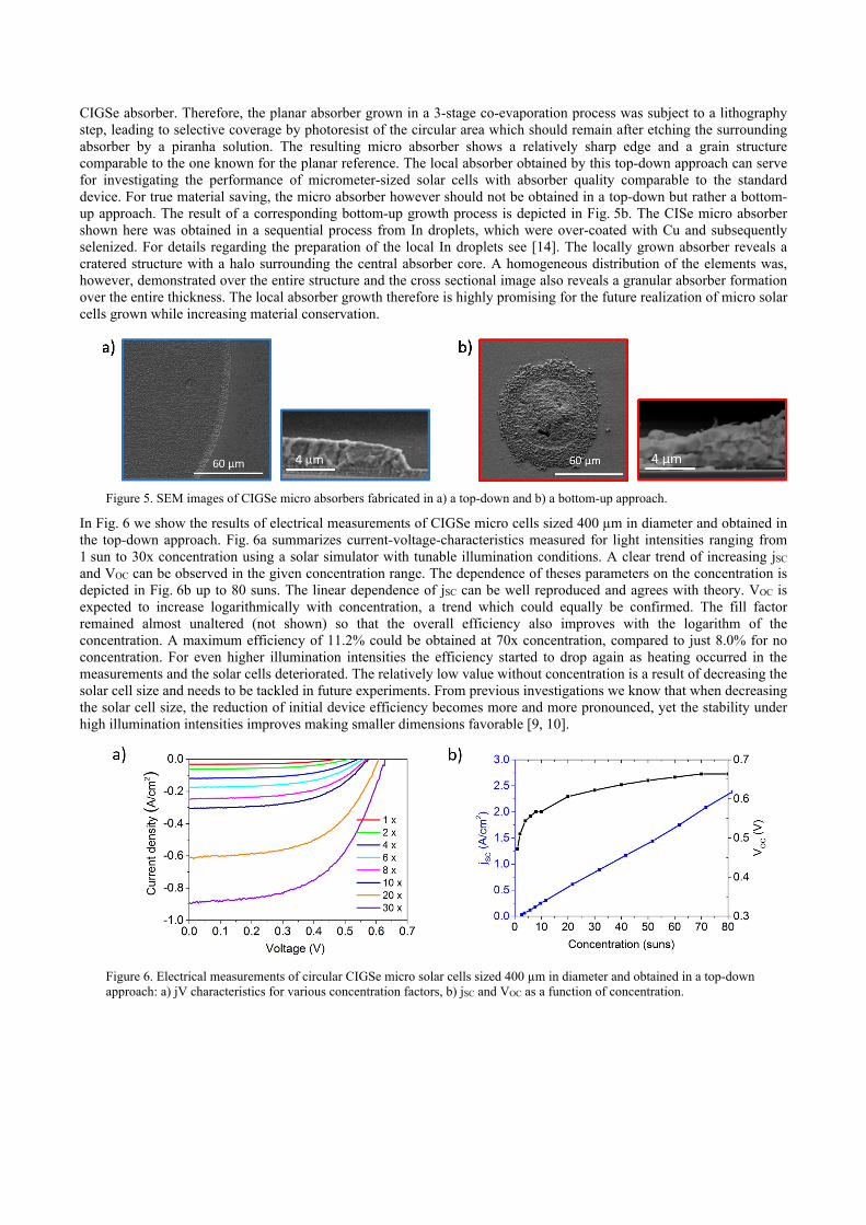
CIGSe absorber. Therefore, the planar absorber grown in a 3-stage co-evaporation process was subject to a lithography step, leading to selective coverage by photoresist of the circular area which should remain after etching the surrounding absorber by a piranha solution. The resulting micro absorber shows a relatively sharp edge and a grain structure comparable to the one known for the planar reference. The local absorber obtained by this top-down approach can serve for investigating the performance of micrometer-sized solar cells with absorber quality comparable to the standard device. For true material saving, the micro absorber however should not be obtained in a top-down but rather a bottom-up approach. The result of a corresponding bottom-up growth process is depicted in Fig. 5b. The CISe micro absorber shown here was obtained in a sequential process from In droplets, which were over-coated with Cu and subsequently selenized. For details regarding the preparation of the local In droplets see [14]. The locally grown absorber reveals a cratered structure with a halo surrounding the central absorber core. A homogeneous distribution of the elements was, however, demonstrated over the entire structure and the cross sectional image also reveals a granular absorber formation over the entire thickness. The local absorber growth therefore is highly promising for the future realization of micro solar cells grown while increasing material conservation.
Figure 5. SEM images of CIGSe micro absorbers fabricated in a) a top-down and b) a bottom-up approach.
In Fig. 6 we show the results of electrical measurements of CIGSe micro cells sized 400 µm in diameter and obtained in the top-down approach. Fig. 6a summarizes current-voltage-characteristics measured for light intensities ranging from 1 sun to 30x concentration using a solar simulator with tunable illumination conditions. A clear trend of increasing jSC and VOC can be observed in the given concentration range. The dependence of theses parameters on the concentration is depicted in Fig. 6b up to 80 suns. The linear dependence of jSC can be well reproduced and agrees with theory. VOC is expected to increase logarithmically with concentration, a trend which could equally be confirmed. The fill factor remained almost unaltered (not shown) so that the overall efficiency also improves with the logarithm of the concentration. A maximum efficiency of 11.2% could be obtained at 70x concentration, compared to just 8.0% for no concentration. For even higher illumination intensities the efficiency started to drop again as heating occurred in the measurements and the solar cells deteriorated. The relatively low value without concentration is a result of decreasing the solar cell size and needs to be tackled in future experiments. From previous investigations we know that when decreasing the solar cell size, the reduction of initial device efficiency becomes more and more pronounced, yet the stability under high illumination intensities improves making smaller dimensions favorable [9, 10].
Figure 6. Electrical measurements of circular CIGSe micro solar cells sized 400 µm in diameter and obtained in a top-down approach: a) jV characteristics for various concentration factors, b) jSC and VOC as a function of concentration.

In order to link the behavior of the micro cells under different but spatially homogeneous concentration factors to the realistic concentration distributions emerging by the usage of micro lenses, we perform optical ray tracing simulations (Comsol). The investigated lenses were hemispheres with 1 mm radius arranged in a square grid and made from a refractive index 1.5 material. The substrate was made of the same material, whereas light was incident from the opposite side via air (wavelength 543 nm). Fig. 7a gives the overview of the concentration distribution behind the lens revealing the focusing behavior. Different planes are marked with distances of L1 = 1.5 mm, L2 = 1.6 mm, L3 = 1.7 mm and L4 = 1.8 mm from the rear of the lens, the latter being closest to the back focal length of 2.0 mm for this configuration [15]. The horizontal dimensions investigated correspond to a spot diameter of 100 µm. In Fig. 7b we give the maps of concentration distribution in the planes corresponding to the above distances L1 - L4. The local power flow was obtained by summing the power of all rays passing through each individual volume element over time and considering the phase velocity of light passing the lens medium. Concentration factors were then derived by relating to the input power flow of 1000 W/m2, which corresponds to one sun. An increasing concentration in the center point and a broadening of the main peak are observed as we move closer to the focus. The secondary high concentration ring, however, is moving closer to the main peak, leading to an overall decrease of the area where the average highest concentration is found and an increase in lateral concentration variations. A maximum concentration of approx. 10,000 suns is reached at the center point. These high concentration values could theoretically lead to huge efficiency enhancements, yet they may also be detrimental for the stability of the solar cells. Furthermore, the high concentrations will lead to heating and adequate thermal management is required. In the end, a distance different from the focal plane has to be chosen in order to provide adequate concentration values and a reasonably homogeneous distribution. Concentration factors exceeding 100 suns and a mostly homogeneous concentration distribution are found for the distance of L1 = 1.5 mm from this lens, i.e. the plane furthest from focus investigated here. Fig. 7c summarizes the concentration profiles taken through the focal spot for the different planes investigated, which supports the choice of appropriate distance at which to place the micro solar cells.
Figure 7. Optical simulations of hemispherical micro lens made from n = 1.5 material on such one: a) ray propagation, lines corresponding to distances of L1 = 1.5 mm, L2 = 1.6 mm, L3 = 1.7 mm and L3 = 1.8 mm from the lens (not to scale: y-range 1.3 mm, x-range 0.1 mm), b) concentration distributions in the different planes, spot diameter 100 µm (same color scale as in a), c) corresponding line profiles through the focal spots.
4. CONCLUSIONS
Ultra-thin absorbers with a CIGSe thickness of less than 500 nm offer material saving by a factor of approximately 5 compared to standard devices. The initial loss in absorption can be well compensated by the integration of dielectric nanostructures leading to light localization inside the ultra-thin absorber. Integration at the rear interface is most beneficial which can additionally enable exploitation of electrical benefits which arise from the formation of point contacts. In this way efficiencies beyond 10% could be achieved for the ultra-thin devices. Despite this efficiency only achieving half of the record efficiency, the thickness reduction results in an efficiency per volume increase by a factor of 2.5. For the micrometer-sized solar cells the material saving factor correlates with the concentration values achieved. In our experimental example this was above 50, from simulating the focusing behavior of lenses it could easily be higher. Thus, compared to the ultra-thin devices, the material saving can be much higher given that solar cells obtained from locally grown absorbers are available. The reduced efficiencies of micrometer-sized and in particular locally grown solar cells still need to be overcome. Yet, even if only half of the efficiency of the record devices is obtained for the micro

concentrator solar cells, due to their huge material saving potential they offer an efficiency increase per volume beyond 25. In the future, further work will be required to continuously improve these novel configurations and bring them towards the market.
ACKNOWLEDGMENT
The authors would like to thank M. Kirsch for ZnO sputtering and grid deposition as well as F. Ringleb for the preparation of In droplets. Funding from the Helmholtz Association for the Young Investigator Group VH-NG-928 within the Initiative and Networking fund is greatly acknowledged. The research leading to these results has received funding from the European Union Seventh Framework Programme (FP7/2007-2013) under Grant Agreement No. 609788. Financial support from the Deutsche Forschungsgemeinschaft (DFG) through SCHM 2554/3-1 is acknowledged. Part of this work was done using resources from the BerOSE Joint Lab for Optical Simulations.
REFERENCES
[1] https://www.zsw-bw.de/en/newsroom/news/news-detail/news/detail/News/zsw-sets-new-world-record-for-thin-film-solar-cells.html (2016).
[2] British Geological Survey: Risk List http://www.bgs.ac.uk/mineralsuk/statistics/risklist.html (2015). [3] C. Morioka, K. Shimazaki, S. Kawakita et al., “First flight demonstration of film-laminated InGaP/GaAs and
CIGS thin-film solar cells by JAXA's small satellite in LEO,” Progress in Photovoltaics: Research and Applications, 19(7), 825-833 (2011).
[4] H. A. Atwater, and A. Polman, “Plasmonics for improved photovoltaic devices,” Nature Materials, 9, 205-213 (2010).
[5] M. Gu, Z. Ouyang, B. Jia et al., “Nanoplasmonics: a frontier of photovoltaic solar cells,” Nanophotonics, 1(3-4), 235-248 (2012).
[6] C. van Lare, G. Yin, A. Polman et al., “Light coupling and trapping in ultrathin Cu(In,Ga)Se2 solar cells using dielectric scattering patterns,” ACS Nano, 9(10), 9603-9613 (2015).
[7] G. Yin, P. Manley, and M. Schmid, “Light absorption enhancement for ultra-thin Cu(In1−xGax)Se2 solar cells using closely packed 2-D SiO2 nanosphere arrays,” Solar Energy Materials and Solar Cells, 153, 124-130 (2016).
[8] J. Yoon, A. J. Baca, S. I. Park et al., “Ultrathin silicon solar microcells for semitransparent, mechanically flexible and microconcentrator module designs,” Nature Materials, 7(11), 907-915 (2008).
[9] M. Paire, L. Lombez, F. Donsanti et al., “Physics of Cu(In,Ga)Se2 microcells under ultrahigh illumination intensities,” Proceedings of SPIE, 8620, 86200Z/1-86200Z/7 (2013).
[10] B. Reinhold, M. Schmid, D. Greiner et al., “Monolithically interconnected lamellar Cu(In,Ga)Se2 micro solar cells under full white light concentration,” Progress in Photovoltaics: Research and Applications, 23(12), 1929-1939 (2015).
[11] T. Negami, S. Nishiwaki, Y. Hashimoto et al., “Effect of absorber thickness on performance of Cu(In,Ga)Se2 solar cells,” 2nd World Conference and Exhibition on Photovoltaic Solar Energy Conversion, Vienna, Austria, 1181-1184 (1998).
[12] M. Schmid, P. Manley, A. Ott et al., “Nanoparticles for light management in ultra-thin chalcopyrite solar cells,” JMR Invited Feature Paper, 31, 3273-3289, (2016).
[13] M. Schmid, P. Andrae, and P. Manley, “Plasmonic and photonic scattering and near fields of nanoparticles,” Nanoscale Research Letters, 9, 50/1-50/9 (2014).
[14] F. Ringleb, K. Eylers, T. Teubner et al., “Regularly arranged indium islands on glass/molybdenum substrates upon femtosecond laser and physical vapor deposition processing,” Applied Physics Letters, 108(11), 111904 (2016).
[15] M. Schmid, and P. Manley, “Nano- and microlenses as concepts for enhanced performance of solar cells,” Journal of Photonics for Energy, 5(1), 057003 (2014).